WO2017082653A1 - Dispositif électronique et procédé de charge sans fil dans un dispositif électronique - Google Patents
Dispositif électronique et procédé de charge sans fil dans un dispositif électronique Download PDFInfo
- Publication number
- WO2017082653A1 WO2017082653A1 PCT/KR2016/012940 KR2016012940W WO2017082653A1 WO 2017082653 A1 WO2017082653 A1 WO 2017082653A1 KR 2016012940 W KR2016012940 W KR 2016012940W WO 2017082653 A1 WO2017082653 A1 WO 2017082653A1
- Authority
- WO
- WIPO (PCT)
- Prior art keywords
- wireless power
- electronic device
- power transmission
- frequency
- controller
- Prior art date
Links
- 238000000034 method Methods 0.000 title claims description 40
- 230000005540 biological transmission Effects 0.000 claims abstract description 172
- 238000006243 chemical reaction Methods 0.000 claims abstract description 123
- 230000004044 response Effects 0.000 claims abstract description 4
- 230000006698 induction Effects 0.000 claims description 67
- 238000004891 communication Methods 0.000 claims description 45
- 230000008859 change Effects 0.000 claims description 11
- 230000005855 radiation Effects 0.000 claims description 6
- 230000005669 field effect Effects 0.000 claims description 4
- 229910044991 metal oxide Inorganic materials 0.000 claims description 2
- 150000004706 metal oxides Chemical class 0.000 claims description 2
- 239000004065 semiconductor Substances 0.000 claims description 2
- 230000006870 function Effects 0.000 description 34
- 239000003990 capacitor Substances 0.000 description 23
- 238000005516 engineering process Methods 0.000 description 9
- 230000001413 cellular effect Effects 0.000 description 8
- 238000010586 diagram Methods 0.000 description 8
- 230000008878 coupling Effects 0.000 description 7
- 238000010168 coupling process Methods 0.000 description 7
- 238000005859 coupling reaction Methods 0.000 description 7
- 230000014509 gene expression Effects 0.000 description 7
- 230000001939 inductive effect Effects 0.000 description 7
- 230000008569 process Effects 0.000 description 6
- 238000012545 processing Methods 0.000 description 4
- 238000002955 isolation Methods 0.000 description 3
- 230000003287 optical effect Effects 0.000 description 3
- XLYOFNOQVPJJNP-UHFFFAOYSA-N water Substances O XLYOFNOQVPJJNP-UHFFFAOYSA-N 0.000 description 3
- WQZGKKKJIJFFOK-GASJEMHNSA-N Glucose Natural products OC[C@H]1OC(O)[C@H](O)[C@@H](O)[C@@H]1O WQZGKKKJIJFFOK-GASJEMHNSA-N 0.000 description 2
- 239000008280 blood Substances 0.000 description 2
- 210000004369 blood Anatomy 0.000 description 2
- 238000002591 computed tomography Methods 0.000 description 2
- 238000013461 design Methods 0.000 description 2
- 238000001514 detection method Methods 0.000 description 2
- 230000000694 effects Effects 0.000 description 2
- 230000005611 electricity Effects 0.000 description 2
- 230000007613 environmental effect Effects 0.000 description 2
- 239000011521 glass Substances 0.000 description 2
- 239000008103 glucose Substances 0.000 description 2
- 238000002583 angiography Methods 0.000 description 1
- 238000003491 array Methods 0.000 description 1
- 230000036772 blood pressure Effects 0.000 description 1
- 230000001419 dependent effect Effects 0.000 description 1
- -1 electricity Substances 0.000 description 1
- 238000002567 electromyography Methods 0.000 description 1
- 238000002474 experimental method Methods 0.000 description 1
- 239000002803 fossil fuel Substances 0.000 description 1
- 238000009434 installation Methods 0.000 description 1
- 230000002452 interceptive effect Effects 0.000 description 1
- 238000002595 magnetic resonance imaging Methods 0.000 description 1
- 238000012986 modification Methods 0.000 description 1
- 230000004048 modification Effects 0.000 description 1
- 239000004984 smart glass Substances 0.000 description 1
- 239000007787 solid Substances 0.000 description 1
- 230000003068 static effect Effects 0.000 description 1
- 230000001360 synchronised effect Effects 0.000 description 1
- 238000012546 transfer Methods 0.000 description 1
- 229910052724 xenon Inorganic materials 0.000 description 1
- FHNFHKCVQCLJFQ-UHFFFAOYSA-N xenon atom Chemical compound [Xe] FHNFHKCVQCLJFQ-UHFFFAOYSA-N 0.000 description 1
Images


Classifications
-
- H—ELECTRICITY
- H02—GENERATION; CONVERSION OR DISTRIBUTION OF ELECTRIC POWER
- H02J—CIRCUIT ARRANGEMENTS OR SYSTEMS FOR SUPPLYING OR DISTRIBUTING ELECTRIC POWER; SYSTEMS FOR STORING ELECTRIC ENERGY
- H02J50/00—Circuit arrangements or systems for wireless supply or distribution of electric power
- H02J50/10—Circuit arrangements or systems for wireless supply or distribution of electric power using inductive coupling
- H02J50/12—Circuit arrangements or systems for wireless supply or distribution of electric power using inductive coupling of the resonant type
-
- H02J7/025—
-
- G—PHYSICS
- G06—COMPUTING; CALCULATING OR COUNTING
- G06F—ELECTRIC DIGITAL DATA PROCESSING
- G06F1/00—Details not covered by groups G06F3/00 - G06F13/00 and G06F21/00
-
- G—PHYSICS
- G06—COMPUTING; CALCULATING OR COUNTING
- G06F—ELECTRIC DIGITAL DATA PROCESSING
- G06F1/00—Details not covered by groups G06F3/00 - G06F13/00 and G06F21/00
- G06F1/26—Power supply means, e.g. regulation thereof
-
- H—ELECTRICITY
- H01—ELECTRIC ELEMENTS
- H01F—MAGNETS; INDUCTANCES; TRANSFORMERS; SELECTION OF MATERIALS FOR THEIR MAGNETIC PROPERTIES
- H01F38/00—Adaptations of transformers or inductances for specific applications or functions
- H01F38/14—Inductive couplings
-
- H—ELECTRICITY
- H02—GENERATION; CONVERSION OR DISTRIBUTION OF ELECTRIC POWER
- H02J—CIRCUIT ARRANGEMENTS OR SYSTEMS FOR SUPPLYING OR DISTRIBUTING ELECTRIC POWER; SYSTEMS FOR STORING ELECTRIC ENERGY
- H02J50/00—Circuit arrangements or systems for wireless supply or distribution of electric power
-
- H—ELECTRICITY
- H02—GENERATION; CONVERSION OR DISTRIBUTION OF ELECTRIC POWER
- H02J—CIRCUIT ARRANGEMENTS OR SYSTEMS FOR SUPPLYING OR DISTRIBUTING ELECTRIC POWER; SYSTEMS FOR STORING ELECTRIC ENERGY
- H02J50/00—Circuit arrangements or systems for wireless supply or distribution of electric power
- H02J50/10—Circuit arrangements or systems for wireless supply or distribution of electric power using inductive coupling
-
- H—ELECTRICITY
- H02—GENERATION; CONVERSION OR DISTRIBUTION OF ELECTRIC POWER
- H02J—CIRCUIT ARRANGEMENTS OR SYSTEMS FOR SUPPLYING OR DISTRIBUTING ELECTRIC POWER; SYSTEMS FOR STORING ELECTRIC ENERGY
- H02J50/00—Circuit arrangements or systems for wireless supply or distribution of electric power
- H02J50/60—Circuit arrangements or systems for wireless supply or distribution of electric power responsive to the presence of foreign objects, e.g. detection of living beings
-
- H—ELECTRICITY
- H02—GENERATION; CONVERSION OR DISTRIBUTION OF ELECTRIC POWER
- H02J—CIRCUIT ARRANGEMENTS OR SYSTEMS FOR SUPPLYING OR DISTRIBUTING ELECTRIC POWER; SYSTEMS FOR STORING ELECTRIC ENERGY
- H02J50/00—Circuit arrangements or systems for wireless supply or distribution of electric power
- H02J50/80—Circuit arrangements or systems for wireless supply or distribution of electric power involving the exchange of data, concerning supply or distribution of electric power, between transmitting devices and receiving devices
-
- H—ELECTRICITY
- H02—GENERATION; CONVERSION OR DISTRIBUTION OF ELECTRIC POWER
- H02J—CIRCUIT ARRANGEMENTS OR SYSTEMS FOR SUPPLYING OR DISTRIBUTING ELECTRIC POWER; SYSTEMS FOR STORING ELECTRIC ENERGY
- H02J7/00—Circuit arrangements for charging or depolarising batteries or for supplying loads from batteries
- H02J7/007—Regulation of charging or discharging current or voltage
- H02J7/00712—Regulation of charging or discharging current or voltage the cycle being controlled or terminated in response to electric parameters
-
- H—ELECTRICITY
- H02—GENERATION; CONVERSION OR DISTRIBUTION OF ELECTRIC POWER
- H02M—APPARATUS FOR CONVERSION BETWEEN AC AND AC, BETWEEN AC AND DC, OR BETWEEN DC AND DC, AND FOR USE WITH MAINS OR SIMILAR POWER SUPPLY SYSTEMS; CONVERSION OF DC OR AC INPUT POWER INTO SURGE OUTPUT POWER; CONTROL OR REGULATION THEREOF
- H02M7/00—Conversion of ac power input into dc power output; Conversion of dc power input into ac power output
- H02M7/42—Conversion of dc power input into ac power output without possibility of reversal
- H02M7/44—Conversion of dc power input into ac power output without possibility of reversal by static converters
- H02M7/48—Conversion of dc power input into ac power output without possibility of reversal by static converters using discharge tubes with control electrode or semiconductor devices with control electrode
Definitions
- Various embodiments of the present disclosure relate to an electronic device and a method for wireless charging in the electronic device.
- a mobile terminal such as a portable phone or a PDA (Personal Digital Assistant) uses rechargeable battery.
- electric energy is supplied by a separate charging device that plugs into the mobile device, or otherwise mates the contact terminals of the mobile device to contact terminals of the charging device.
- this type of charging scheme exposes the contact terminals on the mobile device and/or the charging device to the environment. Accordingly, the contact terminals may get contaminated by foreign matter, thereby interfering with charging the battery. Additionally, the exposed contact terminals on the mobile device may make it harder to make the mobile device water resistant.
- Wireless charging, or contactless charging, technology has been developed and used for a number of electronic devices.
- Such wireless charging technology uses wireless power transmission and reception.
- the wireless charging technology allows a battery to be charged by merely putting a mobile device, such as a cell phone, on a charging pad without connecting the portable phone to a separate charging device.
- Wireless charging technology is used for many devices currently, including for wireless electric toothbrushes and wireless electric shavers. It is expected that wireless charging technology will advance significantly as electric cars become more common.
- the inductive coupling scheme has been used for the most part.
- the induction scheme When power is transferred by the inductive coupling scheme, referred to in this disclosure as the induction scheme, current in a primary coil generates a magnetic field, and that magnetic field induces current in a secondary coil.
- Power transmission using inductive coupling has excellent energy transmission efficiency.
- the primary and secondary coils must be very close to each other for efficient energy transfer.
- the resonance inductive coupling scheme is a type of inductive coupling scheme where both the transmitter and the receiver have circuits tuned to a specific frequency.
- Professor Soljacic at MIT demonstrated this wireless charging system in 2005 by transferring power to an electronic device several meters away using Coupled Mode Theory.
- the resonance scheme uses the concept of resonance frequency, where resonance frequency is a characteristic of all objects. An object may preferentially generate or receive energy at its resonance frequency. For example, when a tuning fork is struck, it will vibrate at its resonance frequency. A wine glass near the turning fork with the same resonance frequency will absorb the acoustic energy of the vibrations generated by the tuning fork until the wine glass shatters.
- a power transmitter using the resonance scheme generates a magnetic field of a specific frequency. Energy is transferred via that magnetic field only when there is a receiving device with receiving circuitry that has that resonance frequency. Due to larger distances between the transmitting device and the receiving device, the resonance scheme may have lower energy transmission efficiency than the induction scheme.
- the circuits or systems constituting a transmitter and a receiver are different from each other.
- a transmitter and a receiver may need to be provided for each standard that is supported.
- An aspect of various embodiments of the present disclosure is to provide an electronic device and a method for wireless charging in the electronic device, capable of allowing one circuit to support functions of both a transmitter and a receiver.
- Another aspect of various embodiments of the present disclosure is to provide an electronic device and a method for wireless charging in the electronic device, capable of allowing one circuit to provide a plurality of wireless charging standards.
- an electronic device that includes a power supply configured to supply direct current (DC) power, and a controller configured to: determine a wireless power transmission mode or a wireless power reception mode if an external electronic device is detected, and output a first control signal corresponding to a wireless power transmission frequency supported by the external electronic device from among a plurality of wireless power transmission frequencies if the wireless power transmission mode is determined.
- the electronic device may also include a conversion circuit configured to convert the DC power supplied by the power supply to alternating current (AC) power in response to the first control signal and a wireless power transceiver configured to transmit the AC power from the conversion circuit.
- AC alternating current
- a method for wireless charging in an electronic device includes determining a wireless power transmission mode or a wireless power reception mode if an external electronic device is detected, determining a wireless power transmission frequency supported by the external electronic device from among a plurality of wireless power transmission frequencies if the wireless power transmission mode is determined, converting direct current (DC) power to alternating current (AC) power based on a control signal corresponding to the wireless power transmission frequency, and transmitting the AC power.
- DC direct current
- AC alternating current
- an electronic device and a method for wireless charging in the electronic device may implement, into a single circuit, a transmitter for generating AC power to transmit wireless charging power and a receiver for generating DC power from the received wireless power, thereby contributing to miniaturization and reduced cost of the electronic device.
- an electronic device and a method for wireless charging in the electronic device may implement or configure a coil for transmitting and receiving wireless power with an integrated coil so as to support a plurality of standards for the resonance scheme and the induction scheme, and may selectively transmit wireless charging power according to each standard depending on the control signal from a controller.
- FIG. 1 is a block diagram illustrating a configuration of an electronic device according to various embodiments of the present disclosure
- FIG. 2 is a detailed circuit diagram of an electronic device according to various embodiments of the present disclosure.
- FIG. 3 illustrates a current flow in a wireless power transmission mode of an electronic device according to various embodiments of the present disclosure
- FIGs. 4a and 4b illustrate a detailed current flow in a wireless power transmission mode of an electronic device according to various embodiments of the present disclosure
- FIG. 5 illustrates input waveforms to MOSFET gates according to various embodiments of the present disclosure
- FIG. 6 illustrates an output waveform of a wireless power transceiver according to various embodiments of the present disclosure
- FIG. 7 illustrates a current flow in a wireless power reception mode of an electronic device according to various embodiments of the present disclosure
- FIGs. 8a and 8b illustrate a detailed current flow in a wireless power reception mode of an electronic device according to various embodiments of the present disclosure
- FIGs. 9 and 10 illustrate selection of a wireless charging frequency in a wireless power transmission mode of an electronic device according to various embodiments of the present disclosure
- FIG. 11 illustrates an example of a detailed circuit configuration of a conversion circuit according to various embodiments of the present disclosure
- FIG. 12 illustrates another example of a detailed circuit configuration of a conversion circuit according to various embodiments of the present disclosure
- FIG. 13 illustrates further another example of a detailed circuit configuration of a conversion circuit according to various embodiments of the present disclosure
- FIG. 14 illustrates yet another example of a detailed circuit configuration of a conversion circuit according to various embodiments of the present disclosure
- FIGs. 15a to 15e are flowcharts illustrating a wireless charging procedure in an electronic device according to various embodiments of the present disclosure
- FIG. 16 is a block diagram illustrating a detailed structure of an electronic device according to various embodiments of the present disclosure.
- FIG. 17 is a block diagram of a program module according to various embodiments of the present disclosure.
- an expression such as “having,” “may have,” “comprising,” or “may comprise” indicates existence of a corresponding characteristic (e.g., a numerical value, function, operation, or component) and does not exclude existence of additional characteristic.
- a singular form may include a plurality of forms unless it is explicitly differently represented.
- an expression such as “A and/or B” may include all possible combinations of the listed items.
- “A and/or B” may indicate (1) including at least one A, (2) including at least one B, or (3) including both at least one A and at least one B.
- Expressions such as “first,” “second,” “primarily,” or “secondary,” used in various exemplary embodiments may represent various elements regardless of order and/or importance and do not limit corresponding elements. The expressions may be used for distinguishing one element from another element.
- a first user device and a second user device may represent different user devices regardless of order or importance. Accordingly, a first element may be referred to as a second element without deviating from the scope of the present disclosure, and similarly, a second element may be referred to as a first element.
- first element When it is described that a first element is operatively or communicatively coupled/connected to a second element, the first element can be directly connected to the second element with no intermediate element in between or the first element can be connected to the second element via one or more elements. However, when it is described that a first element is directly connected/coupled to a second element, it means that there is no intermediate element between the first element and the second element.
- the expression “configured to” used in the present disclosure may be replaced with, for example, “suitable for,” “having the capacity to,” “designed to,” “adapted to,” “made to,” or “capable of” according to a situation.
- the expression “configured to” does not always mean only “specifically designed to” by hardware.
- the expression “apparatus configured to” may mean that the apparatus can operate together with another apparatus or component.
- a processor configured to perform A, B, and C may be referring to a generic-purpose processor (such as a CPU or an application processor) that can perform a corresponding operation by executing at least one software program for performing a corresponding operation, where the software program is stored at an exclusive processor (such as an embedded processor) or at a memory device.
- a generic-purpose processor such as a CPU or an application processor
- the software program is stored at an exclusive processor (such as an embedded processor) or at a memory device.
- An electronic device may be, for example, a smart phone, a tablet personal computer (PC), a mobile phone, a video phone, an e-book reader, a desktop PC, a laptop PC, a netbook computer, a workstation, a server, a personal digital assistant (PDA), a portable multimedia player (PMP), an MP3 player, a mobile medical device, a camera, or a wearable device (e.g., smart glasses, a head mounted device (HMD), electronic clothing, an electronic bracelet, an electronic necklace, an electronic App accessory (or appcessory), electronic tattoo, a smart mirror, or a smart watch.).
- PDA personal digital assistant
- PMP portable multimedia player
- MP3 player MP3 player
- the electronic device may be a smart home appliance.
- the smart home appliance may be, for example, a television (TV), a digital video disk (DVD) player, an audio player, a refrigerator, an air conditioner, a cleaner, an oven, a microwave oven, a washer, an air purifier, a set-top box, a home automation control panel, a security control panel, a TV box (e.g., a Samsung HomeSyncTM, an Apple TVTM, or a Google TVTM), a game console (e.g., XboxTM or PlayStationTM), an electronic dictionary, an electronic key, a camcorder or a digital photo frame.
- TV television
- DVD digital video disk
- the electronic device may be one of various medical devices (e.g., various portable medical meters such as a blood glucose meter, a heart rate meter, a blood pressure meter, a temperature meter or the like), magnetic resonance angiography (MRA) machine, magnetic resonance imaging (MRI) machine, computed tomography (CT) machine, a medical camcorder, an ultrasonic device or the like), a navigation device, a global positioning system (GPS) receiver, an event data recorder (EDR), a flight data recorder (FDR), an automotive infotainment device, a marine electronic device (e.g., a marine navigation device, a gyro compass or the like), avionics, a security device, a car head unit, an industrial or home robot, an automatic teller machine (ATM) for banks, point of sales (POS) for shops, or an internet of things (IoT) device (e.g., an electric bulb, various sensors, an electricity or gas meter, a sprinkler
- the electronic device may be a part of the furniture or building/structure, an electronic board, an electronic signature receiving device, a projector, or various meters (e.g., meters for water, electricity, or gas).
- the electronic device may be one or a combination of the above-described devices.
- An electronic device according to some embodiments may be a flexible electronic device.
- an electronic device according to an embodiment of the present disclosure will not be limited to the above-described devices, and may be a new electronic device introduced as technology progresses.
- the term “user” may refer to a person who uses the electronic device, or a device (e.g., an intelligent electronic device) that uses the electronic device.
- FIG. 1 is a block diagram illustrating a configuration of an electronic device according to various embodiments of the present disclosure.
- an electronic device 100 may include at least one of a controller 110, a conversion circuit 120, a wireless power transceiver 130, a transmission/reception switch 140, first and second frequency controllers 151 and 152, a power supply 160, a communication unit 170, a sensor unit 180, a voltage converter 191, a charging circuit 192 and a battery 193.
- the controller 110 may determine whether the electronic device 100 is in a wireless power transmission (Tx) mode for transmitting wireless power to another electronic device, or in a wireless power reception (Rx) mode for receiving wireless power from another electronic device.
- Tx wireless power transmission
- Rx wireless power reception
- the method of determining the wireless power transmission mode or the wireless power reception mode may be implemented in many different ways.
- the controller 110 may determine the wireless power transmission mode or the wireless power reception mode by detecting a load change using at least one coil provided in the wireless power transceiver 130 by means of the sensor unit 180.
- the controller 110 may determine the wireless power transmission mode or the wireless power reception mode using an in-band signal received through the wireless power transceiver 130. Moreover, according to various embodiments of the present disclosure, the controller 110 may determine the wireless power transmission mode or the wireless power reception mode based on an out-of-band signal received from another electronic device through the communication unit 170.
- the controller 110 may determine a wireless charging scheme (e.g., the induction scheme or the resonance scheme) or a wireless charging frequency (e.g., 100 ⁇ 205kHz, 100 ⁇ 300kHz, 6.78MHz or the like) supported by another electronic device detected for wireless charging from the in-band signal or the out-of-band signal.
- a wireless charging scheme e.g., the induction scheme or the resonance scheme
- a wireless charging frequency e.g., 100 ⁇ 205kHz, 100 ⁇ 300kHz, 6.78MHz or the like
- the controller 110 may control the transmission/reception switch 140 to switch a connection path of the conversion circuit 120 to the voltage converter 191.
- the electronic device 100 may receive wireless power through the wireless power transceiver 130 (e.g., a first wireless power transceiver 131 or a second wireless power transceiver 132).
- the wireless power which is alternating current (AC) power
- received through the wireless power transceiver 130 may be converted into direct current (DC) power by the conversion circuit 120, and the wireless power converted (e.g., rectified) into the DC current may be provided to the voltage converter 191 through the transmission/reception switch 140.
- DC direct current
- the voltage converter 191 may convert the wireless power received through the conversion circuit 120 to a preset voltage.
- the voltage converter 191 may convert the input voltage to an output voltage of 5V.
- the minimum value and maximum value of a voltage that can be applied to the input of the voltage converter 191 may be set in advance.
- the voltage may be converted by the voltage converter 191, and then, used to charge the battery 193 through the charging circuit 192.
- the charging circuit 192 may operate under control of the controller 110, and the controller 110 may be provided with a variety of charging-related information through the charging circuit 192.
- the controller 110 may control the transmission/reception switch 140 to switch a connection path of the conversion circuit 120 to the power supply 160 rather than to the voltage converter 191. Accordingly, the power supply 160 may supply DC power to the conversion circuit 120 via the transmission/reception switch 140.
- the power supply 160 may be provided with power from an external power supply such as a wall adaptor or a travel adaptor, and may also be provided with power from the battery 193, or another battery or a rechargeable battery provided in the electronic device 100.
- the controller 110 may generate a control signal corresponding to a wireless power transmission frequency that the controller 110 desires to transmit to the conversion circuit 120, and transmit the generated control signal to the conversion circuit 120.
- the conversion circuit 120 may convert the DC power supplied from the power supply 160 through the transmission/reception switch 140 into AC power corresponding to the frequency and/or the wireless transmission scheme specified in the control signal provided by the controller 110.
- the AC power converted by the conversion circuit 120 may be provided to the wireless power transceiver 130.
- the wireless power transceiver 130 may transmit the AC power from the conversion circuit 120 to the electronic device that the wireless power transceiver 130 desires to charge.
- the electronic device 100 when the electronic device 100 provides a plurality of wireless charging schemes (e.g., the induction scheme, the resonance scheme, and the like) and/or wireless charging frequencies (e.g., 100 ⁇ 205kHz, 100 ⁇ 300kHz, 6.78MHz or the like), the electronic device 100, when in the wireless power transmission mode, may determine the charging scheme(s) supported by the electronic device that is to be charged, thereby providing wireless charging power with the relevant wireless charging scheme or wireless charging frequency.
- wireless charging schemes e.g., the induction scheme, the resonance scheme, and the like
- wireless charging frequencies e.g., 100 ⁇ 205kHz, 100 ⁇ 300kHz, 6.78MHz or the like
- the controller 110 may receive a control signal corresponding to the first frequency through the first frequency controller 151 by controlling of the controller 110, and output a control signal corresponding to the received control signal to the conversion circuit 120. Furthermore, when another electronic device that the electronic device 100 desires to charge supports a wireless charging scheme by a second frequency, the controller 110 may receive a control signal corresponding to the second frequency through the second frequency controller 152151 by controlling of the controller 110, and output a control signal corresponding to the received control signal to the conversion circuit 120.
- the electronic device 100 may include three or more frequency controllers.
- the first frequency controller 151 and the second frequency controller 152 may be replaced by a controller of a first wireless charging scheme (e.g., the induction scheme) and a controller of a second wireless charging scheme (e.g., the resonance scheme), respectively.
- the first frequency controller 151 and the second frequency controller 152 may be integrated in the controller 110.
- the first frequency controller 151 and the second frequency controller 152 may be implemented so as to use the same wireless charging scheme (e.g., the induction scheme) and output control signals corresponding to different or similar frequencies.
- the first frequency controller 151 and/or the second frequency controller 152 may include an oscillator for outputting the desired frequency signal. Furthermore, the first frequency controller 151 and/or the second frequency controller 152 may output signal, data or information corresponding to the desired frequency, and may output a clock signal corresponding to the desired frequency.
- the controller 110 may output a control signal capable of controlling the conversion circuit 120 so as to receive a signal corresponding to the relevant frequency or the relevant wireless charging scheme from the first frequency controller 151 or the second frequency controller 152, and generate AC power corresponding to the relevant frequency or the relevant wireless charging scheme in the conversion circuit 120.
- a detailed configuration of the conversion circuit 120 will be described in detail below in the description of FIGs. 2 to 14.
- the wireless power transceiver 130 may include a plurality of first and second wireless power transceivers 131 and 132 depending on the wireless charging scheme and/or wireless charging frequency supported by the electronic device 100. For example, if there are two wireless charging schemes or wireless charging frequencies, the first wireless power transceiver 131 and the second wireless power transceiver 132 may be provided as shown in FIG. 1.
- the first wireless power transceiver 131 may correspond to the first frequency controller 151 and the second wireless power transceiver 132 may correspond to the second frequency controller 152, but the present disclosure will not be limited thereto.
- the first wireless power transceiver 131 and the second wireless power transceiver 132 may be connected to the conversion circuit 120 independently, and may also be connected to the conversion circuit 120 in parallel as shown in FIG. 1.
- the first wireless power transceiver 131 and the second wireless power transceiver 132 may constitute a circuit so that the first wireless power transceiver 131 and the second wireless power transceiver 132 may be isolated from each other during wireless power transmission/reception. A detailed description thereof will be made below in the description of FIG. 2 and the subsequent drawings.
- the AC power corresponding to the first frequency that is generated in the conversion circuit 120 under control of the first frequency controller 151 may be provided to the first wireless power transceiver 131 and the second wireless power transceiver 132, and the AC power may be wirelessly transmitted through the first wireless power transceiver 131 depending on the circuit configurations of the first wireless power transceiver 131 and the second wireless power transceiver 132.
- the AC power corresponding to the second frequency that is generated in the conversion circuit 120 under control of the second frequency controller 152 may be provided to the first wireless power transceiver 131 and the second wireless power transceiver 132, and the AC power may be wirelessly transmitted through the second wireless power transceiver 132 depending on the circuit configurations of the first wireless power transceiver 131 and the second wireless power transceiver 132.
- the whole or a part of the controller 110 may be included in at least a portion of an application processor (AP) 1610 or a communication module (or a communication processor (CP)) 1620 in FIG. 16.
- AP application processor
- CP communication processor
- the term “function unit” or “module” may refer to a functional or structural combination of hardware for performing the technical concept of various embodiments of the present disclosure and software for running the hardware.
- the function unit or the module may refer to a logical unit of a predetermined code and hardware resources for which the predetermined code is to be executed, and it can be readily understood by those skilled in the art that a function unit or a module does not necessarily refer to a structurally connected code or one type of hardware.
- An electronic device may include a power supply configured to supply direct current (DC) power; a controller configured to determine a wireless power transmission mode or a wireless power reception mode if at least one electronic device is detected, and output a control signal corresponding to a wireless power transmission frequency supportable in the detected electronic device among a plurality of transmittable wireless power transmission frequencies if the wireless power transmission mode is determined; a conversion circuit configured to output the DC power supplied from the power supply as alternating current (AC) power in response to the control signal output from the controller; and a wireless power transceiver configured to transmit the AC power supplied from the conversion circuit to a wireless space.
- DC direct current
- the electronic device may further include a transmission/reception switch configured to receive a control signal from the controller depending on the determination of a wireless power transmission mode or a wireless power reception mode by the controller, and switch a connection path of the conversion circuit to the power supply or a charging circuit depending on the received control signal.
- a transmission/reception switch configured to receive a control signal from the controller depending on the determination of a wireless power transmission mode or a wireless power reception mode by the controller, and switch a connection path of the conversion circuit to the power supply or a charging circuit depending on the received control signal.
- the conversion circuit may convert the AC power received through the wireless power transceiver into DC power in the wireless power reception mode.
- the wireless power transmission frequency may include at least one of a frequency corresponding to a resonance scheme, a frequency corresponding to an induction scheme, or a frequency corresponding to a radio wave radiation scheme.
- the conversion circuit may be implemented with a full-bridge field-effect transistor (FET) circuit configured using four metal oxide semiconductor field-effect transistors (MOSFETs).
- FET field-effect transistor
- the conversion circuit may be implemented with a circuit including two MOSFETs and two diodes.
- the wireless power transceiver may include a plurality of coils each corresponding to each frequency of the plurality of wireless power transmission frequencies.
- the wireless power transceiver may include an induction scheme wireless power transceiver configured to transmit and receive wireless power corresponding to a frequency of an induction scheme; and a resonance scheme wireless power transceiver configured to transmit and receive wireless power corresponding to a frequency of a resonance scheme.
- the induction scheme wireless power transceiver and the resonance scheme wireless power transceiver may be connected to the conversion circuit in parallel.
- the induction scheme wireless power transceiver or the resonance scheme wireless power transceiver may include a coil and at least one capacitor.
- the electronic device 100 may include a smart car.
- the smart car may refer to a car that recognizes its internal/external situations in real time by integrating the next-generation electric/electronic, information communication and control technologies.
- the smart car is also called a connected car. Since the smart car can be driven using an electric battery rather than the fossil fuel, the smart car may be construed to include an electric car.
- the electronic device 100 including the controller 110, the conversion circuit 120, the wireless power transceiver 130, the transmission/reception switch 140, the frequency controllers 151 and 152, the power supply 160, the communication unit 170, the sensor unit 180, the voltage converter 191, the charging circuit 192 and the battery 193 may include an electric car.
- the conversion circuit 120 the wireless power transceiver 130, the transmission/reception switch 140, the frequency controllers 151 and 152, the power supply 160, the sensor unit 180, the voltage converter 191, the charging circuit 192 and the battery 193, their structures, circuits and/or sizes may be changed to correspond to the large capacity of power (the capacity of several to tens of kW).
- the controller 110 may determine whether the electronic device 100 (e.g., an electric car) is in a wireless power transmission mode for wirelessly transmitting power to other electronic devices (e.g., a smart phone, a tablet PC or the like), or in a wireless power reception mode for receiving wireless power from other electronic devices (e.g., an external wireless charging transmission device).
- the electronic device 100 e.g., an electric car
- other electronic devices e.g., a smart phone, a tablet PC or the like
- a wireless power reception mode for receiving wireless power from other electronic devices
- the smart car 100 may determine whether it is in the wireless power transmission mode or the wireless power reception mode, using at least one of a load change of the sensor unit 180, an in-band signal of the wireless power transceiver 130, and an out-band signal of the communication unit 170. Further, the smart car 100 may determine a wireless charting scheme (e.g., the induction scheme or the resonance scheme) or the wireless charging frequency (e.g., 100 ⁇ 205kHz, 100 ⁇ 300kHz, 6.78MHz or the like) supported by other electronic devices, using the in-band signal of the wireless power transceiver 130 and the out-band signal of the communication unit 170.
- a wireless charting scheme e.g., the induction scheme or the resonance scheme
- the wireless charging frequency e.g., 100 ⁇ 205kHz, 100 ⁇ 300kHz, 6.78MHz or the like
- the smart car 100 may determine the wireless power reception mode using the sensor unit 180, the wireless power transceiver 130 or the communication unit 170.
- the power may be wirelessly transmitted to the smart car 100, using a wireless power transmission pad (not shown) connected to the wireless power transmission device (not shown) installed in the place where wireless power can be transmitted.
- the power may be wirelessly transmitted to the smart car 100 through the wireless power transmission pad (not shown) of the wireless power transmission device (not shown), which is located to face the bottom or side of the smart car 100.
- the wireless power transmission pad of the wireless power transmission device may be one or plural in number.
- One wireless power transmission pad may have the capacity of several to tens of kW.
- the wireless power transmission device may rapidly wirelessly charge the smart car 100 using a plurality of wireless power transmission pads.
- the conversion circuit 120, the wireless power transceiver 130, the transmission/reception switch 140, the voltage converter 191, the charging circuit 192 and the battery 193 may also be changed to correspond to the reception (or charging) of the wireless power in the capacity of several to tens of kW.
- the controller 110 of the smart car 100 may switch a connection path of the conversion circuit 120 to the voltage converter 191 by controlling the transmission/reception switch 140, to connect the conversion circuit 120 to the voltage converter 191.
- the smart car 100 in the wireless power reception mode may receive the wireless power transmitted from the wireless power transmission pad (not shown) through the wireless power transceiver 130, or the second wireless power transceiver 132 corresponding to the resonance scheme that is the determined wireless charging scheme.
- the power received through the wireless power transceiver 130 may be converted (e.g., rectified) from AC power to DC power through the conversion circuit 120, and supplied to the voltage converter 191 through the transmission/reception switch 140.
- the voltage converter 191 may convert the wireless power received through the conversion circuit 120 with a preset gain. For example, the voltage converter 191 may convert the wireless power into a voltage at the output end, which corresponds to the capacity of several to tens of kW. The voltage converted through the voltage converter 191 may charge the large-capacity battery 193 mounted in the smart car 100 through the charging circuit 192.
- the charging circuit 192 may operate under control of the controller 110, and the controller 110 may receive a variety of charging-related information through the charging circuit 192.
- the controller 110 may determine the wireless power transmission mode for wirelessly transmitting the power from the electronic device 100 (e.g., an electric car) to other electronic devices (e.g., a smart phone, a tablet PC or the like).
- the electronic device 100 e.g., an electric car
- other electronic devices e.g., a smart phone, a tablet PC or the like.
- the smart car 100 may switch to the wireless power transmission mode for wirelessly transmitting the power to other electronic devices (e.g., the smart phone, the tablet PC or the like) existing in the smart car 100 using the sensor unit 180, the wireless power transceiver 130 or the communication unit 170 included in the smart car 100.
- other electronic devices e.g., the smart phone, the tablet PC or the like
- the smart car 100 may determine the wireless charging scheme (e.g., the induction scheme) and the wireless charging frequency (e.g., 100 ⁇ 205kHz, 100 ⁇ 300kHz, 6.78MHz or the like) for wirelessly charging the wireless power transmission pad (not shown) and other electronic devices located within the smart car 100 using the in-band signal of the wireless power transceiver 130 and the out-band signal of the communication unit 170.
- the wireless charging scheme e.g., the induction scheme
- the wireless charging frequency e.g., 100 ⁇ 205kHz, 100 ⁇ 300kHz, 6.78MHz or the like
- the smart car 100 in the wireless power transmission mode may transmit wireless power to other electronic devices (not shown) through the wireless power transceiver 130, or the first wireless power transceiver 131 corresponding to the induction scheme that is the determined wireless charging scheme.
- the controller 110 of the smart car 100 may connect the conversion circuit 120 to the power supply 160 by controlling the transmission/reception switch 140.
- the power supply 160 may supply AC power to the conversion circuit 120.
- the power supply 160 may be the above-described battery 193, or another battery separately mounted in the smart car 100.
- the controller 110 of the smart car 100 may generate a control signal corresponding to the wireless power transmission frequency of the wireless charging scheme (e.g., the induction scheme), and provide the generated control signal to the conversion circuit 120.
- the wireless charging scheme e.g., the induction scheme
- the conversion circuit 120 may convert the AC power supplied from the power supply 160 into AC power corresponding to the wireless charging scheme and the wireless power transmission frequency depending on the control signal received from the controller 110.
- the wireless power transceiver 130 e.g., the wireless power transmission pad
- the wireless power transceiver 130 may transmit the AC power provided from the conversion circuit 120 to the space to wirelessly transmit the power to other electronic devices.
- the wireless charging scheme in the wireless power reception mode between the smart car 100 and the external wireless power transmission device may be different from the wireless charging scheme between the smart car 100 and other electronic devices (not shown) therein.
- the wireless charging scheme in the wireless power reception mode between the smart car 100 and the external wireless power transmission scheme may be the resonance scheme
- the wireless charging scheme between the smart car 100 and other electronic devices (not shown) therein may be the induction scheme, or vice versa.
- the smart car 100 is not limited thereto.
- the smart car 100 may include three or more frequency controllers (e.g., the electromagnetic scheme or more).
- the first frequency controller 151 and the second frequency controller 152 may be replaced with the first wireless charging scheme (e.g., the induction scheme) controller and the second wireless charging scheme (e.g., the resonance scheme) controller, respectively. Further, the first frequency controller 151 and the second frequency controller 152 may be configured to be integrated in the controller 110.
- the first wireless charging scheme e.g., the induction scheme
- the second wireless charging scheme e.g., the resonance scheme
- the first wireless power transceiver 131 and the second wireless power transceiver 132 may be connected to the conversion circuit 120 independently or in parallel, respectively. Further, the first wireless power transceiver 131 and the second wireless power transceiver 132 may be implemented within one housing (not shown), or may be separately implemented in separate housings (not shown), respectively.
- the first wireless power transceiver 131 and the second wireless power transceiver 132 may be separately implemented, so the first wireless power transceiver 131 may be located outside the smart car and receive wireless power from the external power supply by various wireless charging schemes such as the magnetic resonance scheme, the magnetic induction scheme and the electromagnetic scheme, to charge the battery mounted in the smart car.
- the second wireless power transceiver 132 may transmit the power supplied from the battery mounted in the smart car to charge other electronic devices within the smart car, such as the table PC and the smart phone, by various wireless charging schemes.
- FIG. 1 Various embodiments of the present disclosure configured with the circuit in FIG. 1 will be described below with reference to FIGs. 2 to 14.
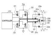
- FIG. 2 is a detailed circuit diagram of an electronic device according to various embodiments of the present disclosure.
- an electronic device 200 may include a controller 210, a conversion circuit 220, a wireless power transceiver 230, a transmission/reception switch 240, frequency controllers 251 and 252, a DC adaptor 260, a buck converter (voltage converter) 291, a charging circuit 292, and a battery 293.
- a controller 210 may include a controller 210, a conversion circuit 220, a wireless power transceiver 230, a transmission/reception switch 240, frequency controllers 251 and 252, a DC adaptor 260, a buck converter (voltage converter) 291, a charging circuit 292, and a battery 293.
- buck converter voltage converter
- the controller 210 may determine whether the electronic device 200 is in a wireless power transmission (Tx) mode for transmitting wireless power to another electronic device, or in a wireless power reception (Rx) mode for receiving wireless power from another electronic device.
- Tx wireless power transmission
- Rx wireless power reception
- the method of determining the wireless power transmission mode or the wireless power reception mode may be implemented in many different ways.
- the controller 210 may determine the wireless power transmission mode or the wireless power reception mode by detecting a load change using at least one coil provided in the wireless power transceiver 230.
- the controller 210 may determine the wireless power transmission mode or the wireless power reception mode using an in-band signal received through the wireless power transceiver 230. Moreover, according to various embodiments of the present disclosure, the controller 210 may determine the wireless power transmission mode or the wireless power reception mode based on an out-of-band signal received from another electronic device.
- the controller 210 may determine a wireless charging scheme (e.g., the induction scheme or the resonance scheme) or a wireless charging frequency (e.g., 100 ⁇ 205kHz, 100 ⁇ 300kHz, 6.78MHz or the like) supported by another electronic device detected for wireless charging from the in-band signal or the out-of-band signal.
- a wireless charging scheme e.g., the induction scheme or the resonance scheme
- a wireless charging frequency e.g., 100 ⁇ 205kHz, 100 ⁇ 300kHz, 6.78MHz or the like
- the controller 210 may control the transmission/reception switch 240 to switch a connection path of the conversion circuit 220 to the buck converter 291.
- the electronic device 200 may receive wireless power through the wireless power transceiver 230 (e.g., via a first coil 231a, a second coil 232a, etc. in a first wireless power transceiver 231, a second wireless power transceiver 232, etc., respectively).
- the first wireless power transceiver 231 and/or the second wireless power transceiver 232 may include at least one coil and at least one capacitor.
- the first wireless power transceiver 231 that supports the induction scheme may include a first coil 231a, a first capacitor 231b and a second capacitor 231c.
- the second wireless power transceiver 232 that supports the resonance scheme may include a second coil 232a and a third capacitor 232b.
- a fourth capacitor 233a and a fifth capacitor 233b may be further provided between the first wireless power transceiver 231 and the second wireless power transceiver 232 for independent operation therebetween.
- the first wireless power transceiver 231 and the second wireless power transceiver 232 may operate in isolation from each other depending on the operating frequency. For example, if it is assumed that the first wireless power transceiver 231 is designed for the resonance scheme that uses a 6.78MHz frequency signal, and the second wireless power transceiver 232 is designed for the induction scheme that uses a 105kHz frequency signal, the first wireless power transceiver 231 and the second wireless power transceiver 232 may operate in isolation from each other during power transmission/reception according to each scheme by the circuit configuration as shown in FIG. 2.
- a 150 kHz signal may be transmitted and received through the wireless power transceiver 230.
- the fourth capacitor 233a and the fifth capacitor 233b configured between the first wireless power transceiver 231 and the second wireless power transceiver 232 are designed to have an impedance of 500 ⁇ or more, the first wireless power transceiver 231 and the second wireless power transceiver 232 may be regarded as circuits that are open to each other with respect to a 150kHz transmission signal.
- a 6.78MHz signal may be transmitted and received through the wireless power transceiver 230. If an inductance of the first coil 231a in the first wireless power transceiver 231 is, for example, 7 ⁇ 10 ⁇ H, since the first wireless power transceiver 231 has an impedance of 300 ⁇ 400 ⁇ , the first coil 231a may be regarded as a circuit that is almost open.
- the wireless power transceivers may be implemented such that the wireless power transceivers may operate independently in isolation from each other with this circuit design.
- the wireless power, which is AC power, received through the wireless power transceiver 230 may be converted into DC power by the conversion circuit 220, and the wireless power converted (e.g., rectified) into the DC power may be provided to the buck converter 291 via the transmission/reception switch 240.
- the conversion circuit 220 may be implemented with a full-bridge FET circuit configured using the first, second, third, and fourth MOSFETs 221, 222, 223 and 224. A detailed operation of the full-bridge FET circuit constituting the conversion circuit 220 will be described below.
- the conversion circuit 220 may be implemented with a half-bridge circuit shown in FIGs. 11 to 14. According to various embodiments of the present disclosure, the conversion circuit 220 may be implemented not only with the above mentioned circuits, but also with any circuit that can provide transmission and reception operations at the same time.
- the buck converter 291 may convert the wireless power received through the conversion circuit 220 to a preset voltage.
- buck converter 291 may convert a voltage of the received wireless power so that the output voltage may be 5V.
- the buck converter 291 may be configured with a circuit that includes at least one coil, at least one capacitor, and/or at least one FET.
- the wireless power whose voltage is converted by the buck converter 291, may be used to charge the battery 293 by the charging circuit 292.
- the charging circuit 292 may operate under control of the controller 210, and the controller 210 may be provided with a variety of charging-related information through the charging circuit 292.
- the controller 210 may control the transmission/reception switch 240 to switch a connection path of the conversion circuit 220 to the DC adaptor 260 rather than to the buck converter 291. Under control of the transmission/reception switch 240, the DC adaptor 260 may supply AC power to the conversion circuit 220.
- the controller 210 may generate a control signal corresponding to the wireless power transmission frequency that the controller 210 desires to transmit to the conversion circuit 220, and provide the generated control signal to the conversion circuit 220.
- the conversion circuit 220 may convert the DC power supplied from the DC adaptor 260 via the transmission/reception switch 240 into AC power corresponding to the frequency and/or the wireless transmission scheme depending on the control signal provided by the controller 210. A detailed operation of the full-bridge FET circuit constituting the conversion circuit 220 will be described below.
- the AC power converted by the conversion circuit 220 may be provided to the wireless power transceiver 230.
- the wireless power transceiver 230 may transmit the AC power provided by the conversion circuit 220, to transmit the charging power to the electronic device that the wireless power transceiver 230 desires to charge.
- the electronic device 200 when the electronic device 200 provides a plurality of wireless charging schemes (e.g., the induction scheme, the resonance scheme, and the like) and/or wireless charging frequencies (e.g., 100 ⁇ 205kHz, 100 ⁇ 300kHz, 6.78MHz or the like), the electronic device 200, in the wireless power transmission mode, may determine the charging scheme supported by the electronic device that the electronic device 200 desires to charge, thereby providing wireless charging power with the correct wireless charging scheme and/or wireless charging frequency.
- wireless charging schemes e.g., the induction scheme, the resonance scheme, and the like
- wireless charging frequencies e.g., 100 ⁇ 205kHz, 100 ⁇ 300kHz, 6.78MHz or the like
- the controller 210 may receive a control signal corresponding to the WPC standard through the frequency controller 251, and output a control signal corresponding to the received control signal to the conversion circuit 220. Furthermore, when another electronic device that the electronic device 200 desires to charge supports the resonance scheme of wireless charging, the controller 210 may receive a frequency (e.g., 6.78MHz) signal of the resonance scheme through the frequency controller 252 (for the resonant scheme), and output a control signal corresponding to the received frequency signal to the conversion circuit 220.
- a frequency e.g., 6.78MHz
- the frequency controller 251 for the induction scheme
- the frequency controller 252 for the resonant scheme
- the electronic device 200 may include three or more frequency controllers with their attendant frequencies that may be design and/or implementation dependent.
- the controller 210 may receive a signal corresponding to the relevant frequency or relevant wireless charging scheme from the frequency controller 251 and/or the frequency controller 252, and output a control signal capable of controlling the conversion circuit 220 so that the conversion circuit 220 may generate AC power corresponding to the relevant frequency and/or relevant wireless charging scheme.
- the wireless power transceiver 230 may include the first and second wireless power transceivers 231 and 232 depending on the wireless charging schemes and/or wireless charging frequencies supported by the electronic device 200. For example, if there are two supported wireless charging schemes with two wireless charging frequencies, the wireless power transceiver 230 may include the first wireless power transceiver 231 and the second wireless power transceiver 232 as shown in FIG. 2.
- the first wireless power transceiver 231 may correspond to wireless power transmission/reception of the induction scheme
- the second wireless power transceiver 232 may correspond to wireless power transmission/reception of the resonance scheme, but the present disclosure will not be limited thereto.
- the first wireless power transceiver 231 and the second wireless power transceiver 232 may be connected in parallel, and connected to the conversion circuit 220 as shown in FIG. 2 such that operation of the first wireless power transceiver 231 does not affect operation of the second wireless power transceiver 232.
- the controller 210 may control the conversion circuit 220 depending on the control signal received from the frequency controller 251. For example, when transmitting in the induction scheme, power may be provided at a frequency corresponding to the induction scheme to the wireless power transceiver 230 for transmission to another electronic device through the first wireless power transceiver 231 in the wireless power transceiver 230. Furthermore, the controller 210 may control the conversion circuit 220 depending on a frequency signal received from the frequency controller 252 to provide power at a frequency corresponding to the resonance scheme to the wireless power transceiver 230 for transmission to another electronic device through the second wireless power transceiver 232 in the wireless power transceiver 230.
- FIGs. 3 to 6 describe an operation of the wireless power transmission mode in the circuit of FIG. 2, and reference will be made to FIGs. 7, 8a and 8b to describe operation of the wireless power reception mode in the circuit of FIG. 2.
- FIG. 3 illustrates a current flow in a wireless power transmission mode of an electronic device according to various embodiments of the present disclosure.
- the controller 210 may control the transmission/reception switch 240 to connect or switch the conversion circuit 220 to the DC adaptor 260.
- DC power from the DC adaptor 260 may be supplied to the conversion circuit 220 via the transmission/reception switch 240.
- the conversion circuit 220 may control ON/OFF state of at least one of the first, second, third, and fourth MOSFETs 221, 222, 223 and 224 depending on the control signal from the controller 210 to output the DC power supplied from the DC adaptor 260 as AC power corresponding to the relevant frequency.
- FIGs. 4a and 4b illustrate a detailed current flow in a wireless power transmission mode of an electronic device according to various embodiments of the present disclosure.
- the controller 210 may turn on the first MOSFET 221 and the fourth MOSFET 224 and turn off the second MOSFET 222 and the third MOSFET 223 to output a positive signal.
- DC power supplied as a VDD voltage may be supplied to the first wireless power transceiver 231 via the first MOSFET 221, and may flow to the fourth MOSFET 224 via the first capacitor 231b, the first coil 231a and the second capacitor 231c of the first wireless power transceiver 231. Accordingly, a positive current may flow in the first coil 231a.
- the controller 210 may turn off the first MOSFET 221 and the fourth MOSFET 224 and turn on the second MOSFET 222 and the third MOSFET 223 to output a negative signal.
- DC power supplied as a VDD voltage may be supplied to the first wireless power transceiver 231 via the second MOSFET 222, and may flow to the third MOSFET 223 via the second capacitor 231c, the first coil 231a and the first capacitor 231b of the first wireless power transceiver 231. Accordingly, a negative current may flow in the first coil 231a.
- an AC current may flow in the second coil 232a by application of the resonance scheme in the same principle.
- the controller 210 may control ON/OFF state of a gate of each of the first, second, third, and fourth MOSFETs 221, 222, 223 and 224 constituting the conversion circuit 220 as in FIGs. 4a and 4b to supply AC power at a frequency corresponding to each wireless charging scheme to the first coil 231a or the second coil 232a.
- the number of MOSFETs, coils and capacitors of, and the configuration and the circuit of the conversion circuit 120 in the smart car 100 may be changed to correspond to the large capacity (e.g., the capacity of several to tens of kW).
- FIG. 5 illustrates input waveforms to MOSFET gates according to various embodiments of the present disclosure
- FIG. 6 illustrates an output waveform of a wireless power transceiver according to various embodiments of the present disclosure.
- a driver waveform of the controller 210 is generated as shown in FIG. 5 and applied appropriately to the gate of each of the first, second, third, and fourth MOSFETs 221, 222, 223 and 224
- an AC power output waveform shown in FIG. 6 may be generated in each of the first and second coils 231a and 232a.
- the output waveforms of the wireless power transceiver of the smart car 100 may be changed to correspond to the large capacity (e.g., the capacity of several to tens of kW).
- FIGs. 7, 8a and 8b describe an operation of the wireless power reception mode in the circuit of FIG. 2.
- FIG. 7 illustrates a current flow in a wireless power reception mode of an electronic device according to various embodiments of the present disclosure.
- the controller 210 may control the transmission/reception switch 240 to connect or switch the conversion circuit 220 to the buck converter 291.
- the conversion circuit 220 may convert AC wireless power received from the wireless power transceiver 230 into DC power and provide the DC power to the buck converter 291.
- the first, second, third, and fourth MOSFETs 221, 222, 223 and 224 provided in the conversion circuit 220 may constitute a full active rectifier circuit to convert the AC power received through the first and second coils 231a and 232a into DC power.
- the current flow may be changed in the wireless power reception mode of the smart car 100 to correspond to the large capacity (e.g., the capacity of several to tens of kW).
- the large capacity e.g., the capacity of several to tens of kW.
- FIGs. 8a and 8b illustrate a detailed current flow in a wireless power reception mode of an electronic device according to various embodiments of the present disclosure.
- the AC current supplied to the conversion circuit 220 may be rectified by the first, second, third, and fourth MOSFETs 221, 222, 223 and 224 constituting the conversion circuit 220, and a DC current may be supplied to the transmission/reception switch 240.
- an AC current by the induction scheme may flow in the second coil 232a by application of the resonance scheme in the same principle.
- the detailed current flow may be changed in the wireless power reception mode of the smart car 100 to correspond to the large capacity (e.g., the capacity of several to tens of kW).
- the large capacity e.g., the capacity of several to tens of kW.
- FIGs. 9 and 10 illustrate selection of a wireless charging frequency in a wireless power transmission mode of an electronic device according to various embodiments of the present disclosure.
- the controller 210 may be provided with a control signal corresponding to the induction scheme by the WPC standard from the frequency controller 251.
- the controller 210 may control ON/OFF states of a gate of each of the first, second, third, and fourth MOSFETs 221, 222, 223 and 224 in the conversion circuit 220 depending on the control signal corresponding to the induction scheme to output AC power at a frequency corresponding to the induction scheme to the first wireless power transceiver 231.
- the first wireless power transceiver 231 may wirelessly transmit the AC power at a frequency corresponding to the induction scheme to the receiving electronic device.
- the controller 210 may be provided with a frequency signal (e.g., a 6.78MHz signal) corresponding to the resonance scheme from the frequency controller 252.
- the controller 210 may control ON/OFF state of a gate of each of the first, second, third, and fourth MOSFETs 221, 222, 223 and 224 in the conversion circuit 220 depending on the control signal corresponding to the resonance scheme to output AC power at a frequency corresponding to the resonance scheme to the second wireless power transceiver 232.
- the second wireless power transceiver 232 may wirelessly transmit the AC power at a frequency corresponding to the resonance scheme to the receiving electronic device.
- controller 210 is switched to the appropriate frequency controller providing the signals corresponding to the respective wireless charging scheme
- a method of selecting a specific wireless charging scheme and generating a control signal may be implemented in various ways.
- two wireless charging schemes are given as an example in FIGs. 9 and 10, the present disclosure may be implemented in the same way for three or more wireless charging schemes.
- FIGs. 11 to 14 describe various exemplary circuit configurations in which the conversion circuit can be implemented.
- FIG. 11 illustrates an example of a detailed circuit configuration of a conversion circuit according to various embodiments of the present disclosure.
- a conversion circuit 1120 according to various embodiments of the present disclosure for received signals may be implemented with the illustrated circuit using two diodes 1121 and 1123 and two MOSFETs 1122 and 1124.
- the conversion circuit 1120 may operate in the same way as the full active rectifier circuit. Furthermore, if the electronic device is in the wireless power transmission mode, the controller may control ON/OFF states of the gates of the two MOSFETs 1122 and 1124 to output AC power to a first wireless power transceiver 1130.
- the first wireless power transceiver 1130 of the induction scheme may include a coil 1131, and capacitors 1132a and 1132b.
- FIG. 12 illustrates another example of a detailed circuit configuration of a conversion circuit according to various embodiments of the present disclosure.
- a conversion circuit 1220 according to various embodiments of the present disclosure may be implemented with the illustrated circuit using two diodes 1223 and 1224 and two MOSFETs 1221 and 1222.
- the conversion circuit 1220 may operate in the same way as the full active rectifier circuit. Furthermore, if the electronic device is in the wireless power transmission mode, the controller may control ON/OFF states of the gates of the two MOSFETs 1221 and 1222 to output AC power to a first wireless power transceiver 1230.
- the first wireless power transceiver 1230 may include a coil 1231, and capacitors 1232a and 1232b.
- FIG. 13 illustrates further another example of a detailed circuit configuration of a conversion circuit according to various embodiments of the present disclosure.
- a conversion circuit 1320 according to various embodiments of the present disclosure may be implemented with the illustrated circuit using two diodes 1321 and 1322 and two MOSFETs 1323 and 1324.
- the conversion circuit 1320 may operate in the same way as the full active rectifier circuit. Furthermore, if the electronic device is in the wireless power transmission mode, the controller may control ON/OFF states of the gates of the two MOSFETs 1323 and 1324 to output AC power to a first wireless power transceiver 1330.
- the first wireless power transceiver 1330 may include a coil 1331, and capacitors 1332a and 1332b.
- FIG. 14 illustrates yet another example of a detailed circuit configuration of a conversion circuit according to various embodiments of the present disclosure.
- a conversion circuit 1420 according to various embodiments of the present disclosure may be implemented with the illustrated circuit using two diodes 1422 and 1424 and two MOSFETs 1421 and 1423.
- the conversion circuit 1420 may operate in the same way as the full active rectifier circuit. Furthermore, if the electronic device is in the wireless power transmission mode, the controller may control ON/OFF states of the gates of the two MOSFETs 1421 and 1423 to output AC power to a first wireless power transceiver 1430.
- the first wireless power transceiver 1430 may include a coil 1431, and capacitors 1432a and 1432b.
- FIGs. 15a to 15e are flowcharts illustrating a wireless charging procedure in an electronic device according to various embodiments of the present disclosure.
- a controller of the electronic device may detect power induced in a coil of a wireless power transceiver by means of a sensor unit. If a load change by an external electronic device is detected by the coil power detection in operation 1504, the controller may determine a change in a Vrect value rectified in a conversion circuit in operation 1506.
- the controller may switch the conversion circuit to a path corresponding to the wireless power reception mode in operation 1510. For example, as described above, in FIG. 1, the controller may switch the path of the conversion circuit 120 to the voltage converter 191.
- the controller may supply the power to a charging circuit in operation 1512, and charge a battery with the power supplied to the charging circuit in operation 1514.
- the controller may determine in operation 1516 whether the load change is made by a foreign object. If it is determined that the power induced in the coil is caused by a foreign object, the controller may perform a preset error handling operation in operation 1530.
- the controller may determine in-band communication for wireless power transmission in operation 1520.
- the controller may switch the conversion circuit to the path corresponding to the wireless power transmission mode in operation 1524. For example, as described above, in FIG. 1, the controller may switch the path of the conversion circuit 120 to the power supply 160.
- the controller may supply power to the conversion circuit in operation 1526, and operate in the wireless power transmission mode of the induction scheme in operation 1528.
- the controller may determine out-of-band communication in operation 1532 of FIG. 15c. As a result of determining out-of-band communication, if the controller determines the wireless power transmission mode of the resonance scheme in operation 1534, the controller may switch the conversion circuit to the path corresponding to the wireless power transmission mode in operation 1536. For example, as described above, in FIG. 1, the controller may switch the path of the conversion circuit 120 to the power supply 160.
- the controller may supply power to the conversion circuit in operation 1538, and operate in the wireless power transmission mode of the resonance scheme in operation 1540.
- the controller may perform in-band authentication for the receiving electronic device that the controller desires to charge, in operation 1542 of FIG. 15d.
- the controller may generate a frequency signal of the induction scheme in operation 1544, and perform a load detection operation using a coil of the electronic device in operation 1546.
- the controller may generate AC power corresponding to the induction scheme in the conversion circuit in operation 1550, and transmit wireless power to the receiving electronic device (i.e., a wireless power receiver) in operation 1552.
- the controller may determine in operation 1554 whether the battery of the receiving electronic device is fully charged, and proceed with the wireless power transmission procedure until the battery is fully charged.
- the controller may perform out-of-band authentication for the receiving electronic device that the controller desires to charge by, for example, Bluetooth low energy (BLE) communication in operation 1556 of FIG. 15e.
- BLE Bluetooth low energy
- the controller may generate a frequency signal of the resonance scheme in operation 1558, and increase the transmission power so as to apply a Vrect voltage in operation 1560.
- the controller determines in operation 1562 whether a sufficient Vrect voltage is applied to the receiving electronic device, and if sufficient Vrect voltage is applied, the controller may generate AC power corresponding to the resonance scheme to the conversion circuit in the conversion circuit in operation 1564, and transmit wireless power to the receiving electronic device (i.e., a wireless power receiver) in operation 1566.
- the controller may determine in operation 1568 whether the battery of the receiving electronic device is fully charged, and proceed with the wireless power transmission procedure until the battery is fully charged.
- At least one of the operations illustrated in FIGs. 15a to 15e may be omitted in execution, and at least one other operation may be added between the operations. Furthermore, the operations illustrated in FIGs. 15a to 15e may be processed in the order shown, and the execution order of at least one operation may be exchanged with the execution order of another operation.
- a method for wireless charging in an electronic device may include determining a wireless power transmission mode or a wireless power reception mode if at least one electronic device is detected; determining a wireless power transmission frequency supportable in the detected electronic device among a plurality of transmittable wireless power transmission frequencies if the wireless power transmission mode is determined; converting direct current (DC) power into alternating current (AC) power based on a control signal corresponding to the determined wireless power transmission frequency; and transmitting the converted AC power to a wireless space.
- DC direct current
- AC alternating current
- the method may further include detecting power applied to a coil of the electronic device; and detecting a load change of an external electronic device from the detected power.
- the method may further include determining the wireless power reception mode if the detected load change of the external electronic device meets a preset condition.
- the method may further include converting AC power applied to the coil into DC power; and charging a battery with the converted DC power.
- the wireless power transmission frequency may include at least one of a frequency corresponding to a resonance scheme, a frequency corresponding to an induction scheme, or a frequency corresponding to a radio wave radiation scheme.
- determining the supportable wireless power transmission frequency may include determining the supportable wireless power transmission frequency using in-band communication by a coil for transmitting and receiving wireless power.
- determining the supportable wireless power transmission frequency may include determining the supportable wireless power transmission frequency using out-of-band communication by a communication unit that provides short-range wireless communication with the detected electronic device.
- determining the supportable wireless power transmission frequency may include determining the supportable wireless power transmission frequency using in-band communication by a coil for transmitting and receiving wireless power; and determining the supportable wireless power transmission frequency using out-of-band communication by a communication unit that provides short-range wireless communication with the detected electronic device, if the supportable wireless power transmission frequency is not determined through the in-band communication.
- determining the supportable wireless power transmission frequency may include transmitting and receiving a signal according to a communication protocol of an induction scheme; and transmitting and receiving a signal according to a communication protocol of a resonance scheme.
- determining the supportable wireless power transmission frequency may include simultaneously transmitting a signal according to a communication protocol of an induction scheme and a signal according to a communication protocol of a resonance scheme.
- FIG. 16 is a block diagram 1600 of an electronic device 1601 according to various embodiments of the present disclosure.
- the electronic device 1601 may include the whole or a part of, for example, the electronic device 100 shown in FIG. 1.
- the electronic device 1601 may include at least one application processor (AP) 1610, a communication module 1616, a subscriber identification module (SIM) card 1624, a memory 1630, a sensor module 1640, an input device 1650, a display 1660, an interface 1670, an audio module 1680, a camera module 1691, a power management module 1695, a battery 1696, an indicator 1697, and a motor 1698.
- AP application processor
- SIM subscriber identification module
- the AP 1610 may control a plurality of hardware or software components by running, for example, an operating system or application program(s), and may process and calculate various data.
- the AP 1610 may be the same as or similar to the controller 110 in FIG. 1 in terms of configuration.
- the AP 1610 may be implemented with, for example, a system on chip (SoC).
- SoC system on chip
- the AP 1610 may further include a graphic processing unit (GPU) and/or an image signal processor.
- the AP 1610 may include at least some (e.g., a cellular module 1621) of the components shown in FIG. 16.
- the AP 1610 may load in volatile memory of the memory 1630, a command or data received from at least one of other components (e.g., a non-volatile memory of the memory 1630) and process the loaded data, and may store a variety of data in a non-volatile memory.
- other components e.g., a non-volatile memory of the memory 1630
- the communication module 1620 may include, for example, the cellular module 1621, a WiFi module 1623, a Bluetooth (BT) module 1625, a GPS module 1627, a near field communication (NFC) module 1628, and a radio frequency (RF) module 1629.
- BT Bluetooth
- BT Bluetooth
- GPS GPS
- NFC near field communication
- RF radio frequency
- the cellular module 1621 may, for example, provide a voice call service, a video call service, a messaging service or an Internet service over a communication network.
- the cellular module 1621 may perform identification and authentication by the electronic device 1601 within the communication network using a subscriber identification module (e.g., the SIM card 1624).
- the cellular module 1621 may have some of the functions that can be provided by the AP 1610.
- the cellular module 1621 may include a communication processor (CP).
- Each of the WiFi module 1623, the BT module 1625, the GPS module 1627 and/or the NFC module 1628 may include, for example, a processor for processing the data transmitted or received through the corresponding module.
- at least some (e.g., two or more) of the cellular module 1621, WiFi module 1623, the BT module 1625, the GPS module 1627 or the NFC module 1628 may be included in one integrated chip (IC) or IC package.
- IC integrated chip
- the RF module 1629 may, for example, transmit and receive communication signals (e.g., RF signals).
- the RF module 1629 may include, for example, a transceiver, a power amplifier module (PAM), a frequency filter, a low noise amplifier (LNA), and/or an antenna.
- PAM power amplifier module
- LNA low noise amplifier
- at least one of the cellular module 1621, the WiFi module 1623, the BT module 1625, the GPS module 1627 and/or the NFC module 1628 may transmit and receive RF signals through a separate RF module.
- the SIM card 1624 may include, for example, a card with a subscriber identification module and/or an embedded SIM.
- the SIM card 1624 may include unique identification information (e.g., integrated circuit card identifier (ICCID)) and/or subscriber information (e.g., international mobile subscriber identity (IMSI)).
- ICCID integrated circuit card identifier
- IMSI international mobile subscriber identity
- the memory 1630 may include, for example, an internal memory 1632 and/or an external memory 1634.
- the internal memory 1632 may include at least one of, for example, volatile memory (e.g., dynamic RAM (DRAM), static RAM (SRAM), synchronous dynamic RAM (SDRAM) or the like) or non-volatile memory (e.g., one time programmable ROM (OTPROM), programmable ROM (PROM), erasable and programmable ROM (EPROM), electrically erasable and programmable ROM (EEPROM), mask ROM, flash ROM, flash memory (e.g., a NAND flash, a NOR flash or the like), hard drive, or solid state drive (SSD)).
- volatile memory e.g., dynamic RAM (DRAM), static RAM (SRAM), synchronous dynamic RAM (SDRAM) or the like
- non-volatile memory e.g., one time programmable ROM (OTPROM), programmable ROM (PROM), erasable and
- the external memory 1634 may further include a flash drive, for example, compact flash (CF), secure digital (SD), micro secure digital (Micro-SD), mini secure digital (Mini-SD), extreme digital (xD), a memory stick or the like.
- CF compact flash
- SD secure digital
- Micro-SD micro secure digital
- Mini-SD mini secure digital
- xD extreme digital
- the external memory 1634 may be functionally and/or physically connected to the electronic device 1601 through various interfaces.
- the sensor module 1640 may, for example, measure the physical quantity or detect the operating status of the electronic device 1601, and convert the measured or detected information into an electrical signal.
- the sensor module 1640 may include, for example, a gesture sensor 1640A, a gyro sensor 1640B, a barometer 1640C, a magnetic sensor 1640D, an accelerometer 1640E, a grip sensor 1640F, a proximity sensor 1640G, a color sensor (e.g., red, green, blue (RGB) sensor) 1640H, a biosensor 1640I, a temperature/humidity sensor 1640J, an illuminance sensor 1640K, and/or a ultra violet (UV) sensor 1640M.
- a gesture sensor 1640A e.g., a gyro sensor 1640B, a barometer 1640C, a magnetic sensor 1640D, an accelerometer 1640E, a grip sensor 1640F, a proximity sensor 1640G, a color sensor (e.g
- the sensor module 1640 may include, for example, an E-nose sensor, an electromyography (EMG) sensor, an electroencephalogram (EEG) sensor, an electrocardiogram (ECG) sensor, an infrared (IR) sensor, an iris sensor and/or a fingerprint sensor.
- the sensor module 1640 may further include a control circuit for controlling at least one or more sensors belonging thereto.
- the electronic device 1601 may further include a processor configured to control the sensor module 1640, separately or as a part of the AP 1610, making it possible to control the sensor module 1640 while the AP 1610 is in a sleep state.
- the input device 1650 may include, for example, a touch panel 1652, a (digital) pen sensor 1654, a key 1656, and/or an ultrasonic input device 1658.
- the touch panel 1652 may use at least one of, for example, capacitive, resistive, infrared and ultrasonic schemes.
- the touch panel 1652 may further include a control circuit.
- the touch panel 1652 may further include a tactile layer, to provide a tactile or haptic feedback to the user.
- the (digital) pen sensor 1654 may be a part of the touch panel 1652, or may include a separate recognition sheet.
- the key 1656 may include, for example, a physical button, an optical key and/or a keypad.
- the ultrasonic input device 1658 may check data by detecting sound waves with a microphone (e.g., a microphone 1688) in the electronic device 1601 using an input tool for generating an ultrasonic signal.
- the display 1660 may include a panel 1662, a hologram device 1664, or a projector 1666.
- the panel 1662 may be implemented to be, for example, flexible, transparent or wearable.
- the panel 1662, together with the touch panel 1652, may be implemented as one module in some embodiments.
- the hologram device 1664 may show stereoscopic images in the air using interference of light.
- the projector 1666 may display images by projecting light on the screen.
- the screen for example, may be disposed inside or outside of the electronic device 1601.
- the display 1660 may further include a control circuit for controlling the panel 1662, the hologram device 1664 or the projector 1666.
- the interface 1670 may include, for example, a high-definition multimedia interface (HDMI) 1672, a universal serial bus (USB) 1674, an optical interface 1676 and/or D-subminiature (D-sub) 1678. Additionally or alternatively, the interface 1670 may include, for example, a mobile high-definition link (MHL) interface, a secure digital (SD) card/multi-media card (MMC) interface, an infrared data association (IrDA) interface, and the like.
- HDMI high-definition multimedia interface
- USB universal serial bus
- D-sub D-subminiature
- the interface 1670 may include, for example, a mobile high-definition link (MHL) interface, a secure digital (SD) card/multi-media card (MMC) interface, an infrared data association (IrDA) interface, and the like.
- MHL mobile high-definition link
- SD secure digital
- MMC multi-media card
- IrDA infrared data association
- the audio module 1680 may convert sound and electrical signals bi-directionally.
- the audio module 1680 may process the sound information that is received or output through a speaker 1682, a receiver 1684, an earphone 1686 or a microphone 1688.
- the camera module 1691 is, for example, a device capable of capturing still images and videos.
- the camera module 1691 may include one or more image sensors (e.g., a front image sensor and/or a rear image sensor), a lens, an image signal processor (ISP), and/or a flash (e.g., an LED or xenon lamp).
- image sensors e.g., a front image sensor and/or a rear image sensor
- ISP image signal processor
- flash e.g., an LED or xenon lamp
- the power management module 1695 may manage power of the electronic device 1601.
- the power management module 1695 may include, for example, a power management integrated circuit (PMIC), a charger integrated circuit (IC), and/or a battery gauge.
- the PMIC may support wired and/or wireless charging scheme.
- the wireless charging scheme may be, for example, the resonance scheme, the induction scheme, and the radio wave (e.g., RF/microwave) radiation scheme, and the power management module 1695 may further include additional circuits (e.g., a coil loop, a resonant circuit, a rectifier or the like) for wireless charging.
- the battery gauge may, for example, measure the remaining capacity, charging voltage, charging current or temperature of the battery 1696.
- the battery 1696 may be, for example, a rechargeable battery and/or a solar battery.
- the indicator 1697 may indicate specific status (e.g., boot status, message status, charging status or the like) of the electronic device 1601 or a part (e.g. the AP 1610) thereof.
- the motor 1698 may convert an electrical signal into mechanical vibrations, thereby generating a vibration or haptic effect.
- the electronic device 1601 may include a processing device (e.g., GPU) for mobile TV support.
- the processing device for mobile TV support may process media data that is based on the standards such as, for example, digital multimedia broadcasting (DMB), digital video broadcasting (DVB) or mediaFLOTM.
- Each of above-described components of the electronic device 1601 may be configured with one or more components, names of which may vary depending on the type of the electronic device 1601.
- the electronic device 1601 may include at least one of the above-described components, some of which may be omitted, or may further include additional other components.
- some of the components of the electronic device 1601 according to various embodiments of the present disclosure may be configured as one entity by being combined to perform the previous functions of the components in the same manner.
- FIG. 17 is a block diagram 1700 of a program module 1710 according to various embodiments of the present disclosure.
- the program module 1710 may include an operating system (OS) for controlling the resources related to an electronic device, and/or a variety of applications (e.g., an application program) that run on the operating system.
- the operating system may be, for example, AndroidTM, iOSTM, WindowsTM, SymbianTM, TizenTM, BadaTM or the like.
- the program module 1710 may include a kernel 1720, a middleware 1730, an application programming interface (API) 1760, and/or application(s) 1770. At least a part of the program module 1710 may be preloaded on the electronic device, or downloaded from a server.
- API application programming interface
- the kernel 1720 may include, for example, a system resource manager 1721 or a device driver 1723.
- the system resource manager 1721 may control, allocate or recover the system resources.
- the system resource manager 1721 may include a process manager, a memory manager, a file system manager or the like.
- the device driver 1723 may include, for example, a display driver, a camera driver, a Bluetooth driver, a shared memory driver, a USB driver, a keypad driver, a WiFi driver, an audio driver, or an inter-process communication (IPC) driver.
- IPC inter-process communication
- the middleware 1730 may provide a function that is required in common by the application(s) 1770, or may provide various functions to the application 1770 through the API 1760 so that the application 1770 may efficiently use the limited system resources within the electronic device.
- the middleware 1730 may include at least one of a runtime library 1735, an application manager 1741, a window manager 1742, a multimedia manager 1743, a resource manager 1744, a power manager 1745, a database manager 1746, a package manager 1747, a connectivity manager 1748, a notification manager 1749, a location manager 1750, a graphic manager 1751, or a security manager 1752.
- the runtime library 1735 may include, for example, a library module that a compiler uses to add a new function through a programming language while the application 1770 is run.
- the runtime library 1735 may perform an input/output (I/O) management function, a memory management function, an arithmetic function or the like.
- the application manager 1741 may, for example, manage the life cycle of at least one of the application(s) 1770.
- the window manager 1742 may manage graphic user interface (GUI) resources that are used on the screen.
- GUI graphic user interface
- the multimedia manager 1743 may determine the format required for playback of various media files, and encode or decode the media files using a codec for the format.
- the resource manager 1744 may manage resources such as source code, memory or storage space for any one of the application(s) 1770.
- the power manager 1745 may manage the battery or power by operating with the basic input/output system (BIOS), and provide power information required for operation of the electronic device.
- the database manager 1746 may create, search or update the database that is to be used by at least one of the application(s) 1770.
- the package manager 1747 may manage installation or update of applications that are distributed in the form of a package file.
- the connectivity manager 1748 may manage wireless connection such as WiFi or Bluetooth.
- the notification manager 1749 may indicate or notify events such as message arrival, appointments and proximity in a manner that doesn’t interfere with the user.
- the location manager 1750 may manage the location information of the electronic device.
- the graphic manager 1751 may manage the graphic effect to be provided to the user, or the user interface related thereto.
- the security manager 1752 may provide various security functions required for the system security or user authentication.
- the middleware 1730 may further include a telephony manager for managing the voice or video call function of the electronic device.
- the middleware 1730 may include a middleware module that forms a combination of various functions of the above-described components.
- the middleware 1730 may provide a module specialized for the type of the operating system in order to provide a differentiated function. Furthermore, the middleware 1730 may dynamically remove some of the existing components, or add new components.
- the API 1760 is a set of API programming functions, and may be provided in a different configuration depending on the operating system. For example, for AndroidTM or iOSTM, the API 1760 may provide one API set per platform, and for TizenTM, the API 1760 may provide two or more API sets per platform.
- the application 1770 may include, for example, one or more applications capable of providing functions such as a home 1771, a dialer 1772, a short message service/multimedia messaging service (SMS/MMS) 1773, an instant message (IM) 1774, a browser 1775, a camera 1776, an alarm 1777, a contact 1778, a voice dial 1779, an Email 1780, a calendar 1781, a media player 1782, an album 1783, a clock 1784, healthcare (e.g., for measuring the quantity of exercise, blood glucose or the like), or environmental information provision (e.g., for providing information about atmospheric pressure, humidity, temperature or the like).
- healthcare e.g., for measuring the quantity of exercise, blood glucose or the like
- environmental information provision e.g., for providing information about atmospheric pressure, humidity, temperature or the like.
- the application 1770 may include an application for supporting information exchange between the electronic device (e.g., the electronic device 100 in FIG. 1) and external electronic devices.
- This application may be referred to as an “information exchange application” for convenience of description.
- the information exchange application may include, for example, a notification relay application for delivering specific information to the external electronic devices, or a device management application for managing the external electronic devices.
- the notification relay application may include a function of delivering notification information generated in other applications (e.g., an SMS/MMS application, an Email application, a healthcare application, an environmental information application or the like) of the electronic device, to the external electronic devices.
- the notification relay application may, for example, receive notification information from an external electronic device, and provide the received notification information to the user.
- the device management application may, for example, manage at least one function (e.g., a function to turn-on/off the external electronic device itself or some components thereof, or the brightness (or the resolution) of the display) of the external electronic device communicating with the electronic device, and may manage (e.g., install, delete or update) an application operating in the external electronic device or a service (e.g., a call service or a messaging service) provided in the external electronic device.
- a function e.g., a function to turn-on/off the external electronic device itself or some components thereof, or the brightness (or the resolution) of the display
- the device management application may, for example, manage at least one function (e.g., a function to turn-on/off the external electronic device itself or some components thereof, or the brightness (or the resolution) of the display) of the external electronic device communicating with the electronic device, and may manage (e.g., install, delete or update) an application operating in the external electronic device or a service (e.g., a call service
- the application 1770 may include an application (e.g., a healthcare application) that is specified depending on the attributes (e.g., the attributes of an electronic device that is a mobile medical device) of the external electronic device.
- the application 1770 may include an application received or downloaded from the external electronic device.
- the application 1770 may include a preloaded application or a third party application that can be downloaded from the server.
- the names of the components of the illustrated program module 1710 may vary depending on the type of the operating system.
- At least a part of the program module 1710 may be implemented by software, firmware, hardware or a combination thereof. At least a part of the program module 1710 may be executed by, for example, a processor (e.g., the AP 1610). At least a part of the program module 1710 may include, for example, a module, a program, a routine, an instruction set and/or a process for performing one or more functions.
- module or “function unit” as used herein may refer to a unit that includes, for example, hardware, software and/or firmware.
- module or “function unit” may be interchangeably used with terms such as, for example, unit, logic, logical block, component, or circuit.
- the “module” or “function unit” may be a minimum unit of an integrally constructed part, or a part thereof.
- the “module” or “function unit” may be the minimum unit for performing one or more functions, or a part thereof.
- the “module” or “function unit” may be implemented mechanically or electronically.
- the “module” or “function unit” may include an application-specific integrated circuit (ASIC) chip, field-programmable gate arrays (FPGAs), and/or a programmable-logic device, which are known or will be developed in the future, and which perform certain operations.
- ASIC application-specific integrated circuit
- FPGAs field-programmable gate arrays
- programmable-logic device which are known or will be developed in the future, and which perform certain operations.
- At least a part of the apparatus (e.g., modules or functions thereof) or method (e.g., operations) according to various embodiments of the present disclosure may be implemented by a command that is stored in computer-readable storage media in the form of, for example, a programming module. If the command is executed by one or more processors (e.g., the controller 110), the one or more processors may perform a function corresponding to the command.
- the computer-readable storage media may be, for example, a storage unit.
- the computer-readable storage media may include magnetic media (e.g., a hard disk, a floppy disk, and magnetic tape), optical media (e.g., a compact disc read only memory (CD-ROM) and a digital versatile disc (DVD)), magneto-optical media (e.g., a floptical disk), and a hardware device (e.g., read only memory (ROM), random access memory (RAM) or flash memory).
- the program command may include not only a machine code such as compiled code, but also a high-level language code that can be executed by the computer using an interpreter.
- the above-described hardware device may be configured to operate as one or more software modules to perform the operations according to various embodiments of the present disclosure, and vice versa.
- a storage medium storing instructions
- the instructions when the instructions are executed by at least one processor, the instructions are set to allow at least one processor to perform at least one operation.
- the operation(s) may include determining a wireless power transmission mode or a wireless power reception mode if at least one electronic device is detected; determining a wireless power transmission frequency supported by the detected electronic device from among a plurality of wireless power transmission frequencies if the wireless power transmission mode is determined; and generating a control signal corresponding to the determined wireless power transmission frequency.
Abstract
Un dispositif électronique selon divers modes de réalisation de la présente invention comprend une alimentation électrique conçue pour fournir un courant continu, un dispositif de commande conçu pour déterminer un mode de transmission de puissance sans fil ou un mode de réception de puissance sans fil si au moins un dispositif électronique est détecté, et émettre un signal de commande indiquant une fréquence de transmission de puissance sans fil prise en charge par le dispositif électronique détecté parmi une pluralité de fréquences de transmission de puissance sans fil si le mode de transmission de puissance sans fil est déterminé, un circuit de conversion conçu pour délivrer le courant continu fourni par l'alimentation électrique en tant que courant alternatif en réponse au signal de commande émis par le dispositif de commande et un émetteur-récepteur de puissance sans fil conçu pour transmettre le courant alternatif fourni.
Priority Applications (3)
| Application Number | Priority Date | Filing Date | Title |
|---|---|---|---|
| EP16864579.4A EP3347965B1 (fr) | 2015-11-10 | 2016-11-10 | Dispositif électronique et procédé de charge sans fil dans un dispositif électronique |
| EP19178179.8A EP3565084B1 (fr) | 2015-11-10 | 2016-11-10 | Dispositif électronique et procédé de charge sans fil dans un dispositif électronique |
| CN201680065904.XA CN108419449B (zh) | 2015-11-10 | 2016-11-10 | 电子设备及用于在电子设备中无线充电的方法 |
Applications Claiming Priority (4)
| Application Number | Priority Date | Filing Date | Title |
|---|---|---|---|
| KR10-2015-0157756 | 2015-11-10 | ||
| KR20150157756 | 2015-11-10 | ||
| KR1020160079387A KR102607172B1 (ko) | 2015-11-10 | 2016-06-24 | 전자 장치 및 전자 장치의 무선 충전 방법 |
| KR10-2016-0079387 | 2016-06-24 |
Publications (1)
| Publication Number | Publication Date |
|---|---|
| WO2017082653A1 true WO2017082653A1 (fr) | 2017-05-18 |
Family
ID=58663854
Family Applications (1)
| Application Number | Title | Priority Date | Filing Date |
|---|---|---|---|
| PCT/KR2016/012940 WO2017082653A1 (fr) | 2015-11-10 | 2016-11-10 | Dispositif électronique et procédé de charge sans fil dans un dispositif électronique |
Country Status (4)
| Country | Link |
|---|---|
| US (2) | US10461583B2 (fr) |
| EP (2) | EP3565084B1 (fr) |
| CN (1) | CN108419449B (fr) |
| WO (1) | WO2017082653A1 (fr) |
Families Citing this family (22)
| Publication number | Priority date | Publication date | Assignee | Title |
|---|---|---|---|---|
| US11241970B2 (en) | 2013-11-14 | 2022-02-08 | Momentum Dynamics Corporation | Method and apparatus for the alignment of vehicles prior to wireless charging |
| TWI622871B (zh) * | 2016-12-30 | 2018-05-01 | 瑞昱半導體股份有限公司 | 顯示控制器之顯示控制晶片及其運作方法 |
| CN110495068A (zh) * | 2017-04-14 | 2019-11-22 | 通用电气公司 | 无线电力收发设备及其相关方法 |
| US11616399B2 (en) * | 2017-05-30 | 2023-03-28 | General Electric Company | Wireless charging device, a receiver device, and a method of operating the same |
| US10523032B2 (en) * | 2017-06-22 | 2019-12-31 | Richtek Technology Corporation | Charging apparatus with multiple power paths |
| KR102434405B1 (ko) * | 2017-10-16 | 2022-08-22 | 삼성전자주식회사 | 전자 장치의 상태에 기반하여, 무선 전력 수신 회로를 비활성화하는 방법 및 그 전자 장치 |
| CN108110904A (zh) * | 2018-01-09 | 2018-06-01 | 珠海格力电器股份有限公司 | 空调设备的供电方法及空调设备 |
| WO2019223004A1 (fr) * | 2018-05-25 | 2019-11-28 | Oppo广东移动通信有限公司 | Dispositif récepteur de charge sans fil et terminal mobile |
| KR102564363B1 (ko) * | 2018-07-27 | 2023-08-08 | 삼성전자 주식회사 | 외부 전자 장치로부터 수신된 식별 정보에 기반하여 무선 충전과 관련된 통신 채널을 제어하는 전자 장치 및 전자 장치의 동작 방법 |
| US10908428B2 (en) * | 2018-09-25 | 2021-02-02 | Facebook Technologies, Llc | Multiple-device system with multiple power and data configurations |
| AU2018443233B2 (en) * | 2018-09-29 | 2022-09-01 | Huawei Technologies Co., Ltd. | Wireless charging method and electronic device |
| US11152974B2 (en) * | 2018-10-31 | 2021-10-19 | Samsung Electronics Co., Ltd. | Wireless communication apparatus and method |
| EP3881411A4 (fr) * | 2018-11-21 | 2022-01-19 | Huawei Digital Power Technologies Co., Ltd. | Communication hors bande pendant une charge de batterie sans fil |
| US11418065B2 (en) * | 2019-01-07 | 2022-08-16 | Ossia Inc. | Portable wireless power charger with integrated wireless power receiving facilities |
| CN109787315A (zh) * | 2019-02-19 | 2019-05-21 | 同方威视技术股份有限公司 | 无线充电装置和包括无线充电装置的安全装置 |
| CN114867632A (zh) * | 2019-12-20 | 2022-08-05 | 动量动力学公司 | 用于在无线充电前的车辆对准的方法和装置 |
| US20230208206A1 (en) * | 2020-04-20 | 2023-06-29 | Lg Electronics Inc. | Wireless power reception device and wireless power transmission device |
| US20230179022A1 (en) * | 2020-04-21 | 2023-06-08 | Lg Electronics Inc. | Wireless power receiver and wireless power transmitter |
| CN111722568B (zh) * | 2020-06-30 | 2021-09-24 | 广州星际悦动股份有限公司 | 电动牙刷的控制方法、装置和中央控制装置 |
| US11843265B2 (en) | 2020-07-02 | 2023-12-12 | Apple Inc. | Wireless power mode switching |
| CN112290611A (zh) * | 2020-09-17 | 2021-01-29 | 安克创新科技股份有限公司 | 用于无线充电的系统 |
| TWI741944B (zh) * | 2021-02-05 | 2021-10-01 | 美律實業股份有限公司 | 無線充電裝置及無線充電切換方法 |
Citations (7)
| Publication number | Priority date | Publication date | Assignee | Title |
|---|---|---|---|---|
| US20110221390A1 (en) | 2010-03-12 | 2011-09-15 | Samsung Electronics Co. Ltd. | Wireless power charging method and apparatus |
| US20130026981A1 (en) * | 2011-07-28 | 2013-01-31 | Broadcom Corporation | Dual mode wireless power |
| US20140070624A1 (en) * | 2012-09-07 | 2014-03-13 | Samsung Electronics Co., Ltd. | Apparatus and method for transmitting and receiving wireless power |
| KR20140123811A (ko) * | 2013-04-15 | 2014-10-23 | 엘지전자 주식회사 | 무선 전력 송수신장치, 무선 충전 시스템 및 무선 충전 시스템의 제어방법 |
| US20150180284A1 (en) | 2013-12-20 | 2015-06-25 | Samsung Electro-Mechanics Co., Ltd. | Apparatus for transmitting and receiving wireless power |
| US20150215006A1 (en) * | 2013-03-13 | 2015-07-30 | Integrated Device Technology, Inc. | Apparatuses and related methods for communication with a wireless power receiver |
| US20150224176A1 (en) | 2012-08-14 | 2015-08-13 | Wockhardt Limited | Pharmaceutical microparticulate compositions of polypeptides |
Family Cites Families (24)
| Publication number | Priority date | Publication date | Assignee | Title |
|---|---|---|---|---|
| KR100736053B1 (ko) * | 2005-10-24 | 2007-07-06 | 삼성전자주식회사 | 유도 방식에 의해 무선으로 전원을 공유하는 장치 및 방법 |
| CN102165667B (zh) * | 2008-09-26 | 2014-09-03 | 株式会社村田制作所 | 无接点充电系统 |
| CN102301577B (zh) | 2009-01-29 | 2014-10-01 | 布鲁萨电子公司 | 用于单相和三相操作的转换器、直流电压源及电池充电器 |
| JP5347708B2 (ja) | 2009-05-18 | 2013-11-20 | トヨタ自動車株式会社 | コイルユニット、非接触電力伝送装置、非接触給電システムおよび車両 |
| KR101648348B1 (ko) * | 2010-04-06 | 2016-08-16 | 삼성전자주식회사 | 무선 전력 충전 기능을 구비한 로봇 청소 시스템 및 제어 방법 |
| US9561730B2 (en) * | 2010-04-08 | 2017-02-07 | Qualcomm Incorporated | Wireless power transmission in electric vehicles |
| TWM393922U (en) * | 2010-07-19 | 2010-12-01 | ming-xiang Ye | Bidirectional wireless charge and discharge device |
| US9602168B2 (en) | 2010-08-31 | 2017-03-21 | Witricity Corporation | Communication in wireless energy transfer systems |
| JP5751884B2 (ja) * | 2011-03-29 | 2015-07-22 | 森永乳業株式会社 | 複極式電解槽 |
| KR101246048B1 (ko) | 2011-07-29 | 2013-04-03 | 이플러스주식회사 | 무정전 전원 공급 시스템 |
| KR20130024757A (ko) | 2011-08-29 | 2013-03-08 | 주식회사 케이더파워 | 이종 충전 방식을 가진 무선 충전 시스템 |
| EP2805402A4 (fr) * | 2012-01-17 | 2015-09-30 | Samsung Electronics Co Ltd | Transmetteur d'énergie sans fil, récepteur d'énergie sans fil et leurs procédés de commande |
| KR101956570B1 (ko) | 2012-09-05 | 2019-03-11 | 엘지전자 주식회사 | 유도 방식과 공진 방식을 지원하는 무선 전력 수신장치 및 무선 전력 수신방법 |
| JP6285441B2 (ja) | 2012-09-07 | 2018-02-28 | アクセス ビジネス グループ インターナショナル リミテッド ライアビリティ カンパニー | 双方向無線電力伝送用のシステム及び方法 |
| KR102007226B1 (ko) | 2013-01-08 | 2019-08-06 | 엘지전자 주식회사 | 이동 단말기 |
| US9530617B2 (en) * | 2013-01-30 | 2016-12-27 | Taiwan Semiconductor Manufacturing Co., Ltd. | In-situ charging neutralization |
| FR3010252B1 (fr) * | 2013-08-30 | 2015-08-21 | Continental Automotive France | Dispositif et procede de charge par couplage magnetique bi-mode pour vehicule automobile |
| KR20150048013A (ko) | 2013-10-25 | 2015-05-06 | 삼성전기주식회사 | 무선 전원 송수신 장치 및 이를 갖는 휴대 단말기 |
| US10014725B2 (en) * | 2013-10-31 | 2018-07-03 | Ge Hybrid Technologies, Llc | Hybrid wireless power transmitting system and method therefor |
| KR102195109B1 (ko) | 2013-11-20 | 2020-12-24 | 삼성전자주식회사 | 무선 충전 장치 및 방법 |
| KR20150107281A (ko) | 2014-03-13 | 2015-09-23 | 엘지이노텍 주식회사 | 무선 전력 송신 장치 및 방법 |
| US10056790B2 (en) * | 2014-06-11 | 2018-08-21 | Enovate Medical Llc | Wireless transfer station for transferring energy |
| KR20160038410A (ko) * | 2014-09-30 | 2016-04-07 | 엘지이노텍 주식회사 | 무선전력전송 시스템 |
| US10389183B2 (en) * | 2014-12-18 | 2019-08-20 | Center For Integrated Smart Sensors Foundation | Multi-mode wireless power receiving device and method |
-
2016
- 2016-11-09 US US15/346,857 patent/US10461583B2/en not_active Expired - Fee Related
- 2016-11-10 EP EP19178179.8A patent/EP3565084B1/fr active Active
- 2016-11-10 CN CN201680065904.XA patent/CN108419449B/zh active Active
- 2016-11-10 WO PCT/KR2016/012940 patent/WO2017082653A1/fr active Application Filing
- 2016-11-10 EP EP16864579.4A patent/EP3347965B1/fr active Active
-
2019
- 2019-08-20 US US16/545,025 patent/US11489368B2/en active Active
Patent Citations (7)
| Publication number | Priority date | Publication date | Assignee | Title |
|---|---|---|---|---|
| US20110221390A1 (en) | 2010-03-12 | 2011-09-15 | Samsung Electronics Co. Ltd. | Wireless power charging method and apparatus |
| US20130026981A1 (en) * | 2011-07-28 | 2013-01-31 | Broadcom Corporation | Dual mode wireless power |
| US20150224176A1 (en) | 2012-08-14 | 2015-08-13 | Wockhardt Limited | Pharmaceutical microparticulate compositions of polypeptides |
| US20140070624A1 (en) * | 2012-09-07 | 2014-03-13 | Samsung Electronics Co., Ltd. | Apparatus and method for transmitting and receiving wireless power |
| US20150215006A1 (en) * | 2013-03-13 | 2015-07-30 | Integrated Device Technology, Inc. | Apparatuses and related methods for communication with a wireless power receiver |
| KR20140123811A (ko) * | 2013-04-15 | 2014-10-23 | 엘지전자 주식회사 | 무선 전력 송수신장치, 무선 충전 시스템 및 무선 충전 시스템의 제어방법 |
| US20150180284A1 (en) | 2013-12-20 | 2015-06-25 | Samsung Electro-Mechanics Co., Ltd. | Apparatus for transmitting and receiving wireless power |
Non-Patent Citations (1)
| Title |
|---|
| See also references of EP3347965A4 |
Also Published As
| Publication number | Publication date |
|---|---|
| US20190379242A1 (en) | 2019-12-12 |
| US11489368B2 (en) | 2022-11-01 |
| EP3347965A4 (fr) | 2018-12-05 |
| EP3347965A1 (fr) | 2018-07-18 |
| US10461583B2 (en) | 2019-10-29 |
| EP3347965B1 (fr) | 2021-02-24 |
| US20170133889A1 (en) | 2017-05-11 |
| CN108419449A (zh) | 2018-08-17 |
| EP3565084B1 (fr) | 2021-03-31 |
| EP3565084A1 (fr) | 2019-11-06 |
| CN108419449B (zh) | 2021-10-26 |
Similar Documents
| Publication | Publication Date | Title |
|---|---|---|
| WO2017082653A1 (fr) | Dispositif électronique et procédé de charge sans fil dans un dispositif électronique | |
| WO2017030411A1 (fr) | Dispositif électronique et procédé de charge filaire et sans fil dans un dispositif électronique | |
| WO2015147503A1 (fr) | Procédé de charge de batterie et dispositif électronique | |
| WO2015126177A1 (fr) | Dispositif électronique et son procédé d'économie d'énergie | |
| WO2015126121A1 (fr) | Procédé pour commander un appareil selon des informations de requête, et appareil prenant en charge le procédé | |
| WO2015030474A1 (fr) | Dispositif électronique et procédé de reconnaissance vocale | |
| WO2017014433A1 (fr) | Procédé de fonctionnement d'un dispositif électronique, et dispositif électronique fonctionnant selon ce procédé | |
| WO2016036128A1 (fr) | Dispositif électronique, procédé de commande de charge par un dispositif électronique et procédé d'alimentation électrique par un dispositif d'alimentation électrique | |
| WO2016105020A1 (fr) | Appareil et procédé de charge d'un dispositif électronique équipé d'une batterie | |
| WO2015034163A1 (fr) | Procédé d'envoi de notification, et dispositif électronique correspondant | |
| WO2015167258A1 (fr) | Procédé et appareil de communication de proximité | |
| WO2017131379A1 (fr) | Dispositif et procédé permettant d'effectuer une communication | |
| WO2017126913A1 (fr) | Dispositif électronique et procédé de communication sans fil à courte portée dans un dispositif électronique | |
| WO2017209502A1 (fr) | Procédé de commande de connexion entre un dispositif électronique et un dispositif de charge, et dispositif pour sa mise en œuvre | |
| WO2018026144A1 (fr) | Procédé de transmission d'énergie et dispositif électronique prenant en charge ledit procédé | |
| WO2020032510A1 (fr) | Dispositif électronique comprenant un stylo électronique et procédé de commande de connexion de communication entre un dispositif électronique et un stylo électronique | |
| WO2019083304A1 (fr) | Dispositif à bobines de transmission de puissance sans fil | |
| WO2016148505A1 (fr) | Appareil électronique et son procédé de fourniture d'informations de batterie | |
| EP3123590A1 (fr) | Procédé de charge de batterie et dispositif électronique | |
| WO2016080761A1 (fr) | Procédé et dispositif électronique pour piloter un capteur d'empreinte digitale | |
| WO2015072783A1 (fr) | Procédé et appareil permettant de faire communiquer des dispositifs électroniques | |
| WO2017003218A1 (fr) | Procédé de commande de multiples batteries et dispositif électronique destiné à le mettre en œuvre | |
| WO2021085850A1 (fr) | Dispositif électronique partageant un dispositif périphérique avec un dispositif électronique externe et son procédé | |
| WO2017043925A1 (fr) | Procédé et dispositif de transmission d'énergie sans fil | |
| WO2017160103A1 (fr) | Procédé et dispositif électronique destinés à fournir une communication sans fil |
Legal Events
| Date | Code | Title | Description |
|---|---|---|---|
| 121 | Ep: the epo has been informed by wipo that ep was designated in this application |
Ref document number: 16864579 Country of ref document: EP Kind code of ref document: A1 |
|
| WWE | Wipo information: entry into national phase |
Ref document number: 2016864579 Country of ref document: EP |
|
| NENP | Non-entry into the national phase |
Ref country code: DE |