WO2017055931A1 - Optical scanning module and optical scanning control device - Google Patents
Optical scanning module and optical scanning control device Download PDFInfo
- Publication number
- WO2017055931A1 WO2017055931A1 PCT/IB2016/001637 IB2016001637W WO2017055931A1 WO 2017055931 A1 WO2017055931 A1 WO 2017055931A1 IB 2016001637 W IB2016001637 W IB 2016001637W WO 2017055931 A1 WO2017055931 A1 WO 2017055931A1
- Authority
- WO
- WIPO (PCT)
- Prior art keywords
- wiring
- optical scanning
- sensor
- drive
- mirror
- Prior art date
Links
Images


Classifications
-
- B—PERFORMING OPERATIONS; TRANSPORTING
- B81—MICROSTRUCTURAL TECHNOLOGY
- B81B—MICROSTRUCTURAL DEVICES OR SYSTEMS, e.g. MICROMECHANICAL DEVICES
- B81B7/00—Microstructural systems; Auxiliary parts of microstructural devices or systems
- B81B7/0006—Interconnects
-
- B—PERFORMING OPERATIONS; TRANSPORTING
- B81—MICROSTRUCTURAL TECHNOLOGY
- B81B—MICROSTRUCTURAL DEVICES OR SYSTEMS, e.g. MICROMECHANICAL DEVICES
- B81B7/00—Microstructural systems; Auxiliary parts of microstructural devices or systems
- B81B7/02—Microstructural systems; Auxiliary parts of microstructural devices or systems containing distinct electrical or optical devices of particular relevance for their function, e.g. microelectro-mechanical systems [MEMS]
-
- G—PHYSICS
- G02—OPTICS
- G02B—OPTICAL ELEMENTS, SYSTEMS OR APPARATUS
- G02B26/00—Optical devices or arrangements for the control of light using movable or deformable optical elements
- G02B26/08—Optical devices or arrangements for the control of light using movable or deformable optical elements for controlling the direction of light
- G02B26/0816—Optical devices or arrangements for the control of light using movable or deformable optical elements for controlling the direction of light by means of one or more reflecting elements
- G02B26/0833—Optical devices or arrangements for the control of light using movable or deformable optical elements for controlling the direction of light by means of one or more reflecting elements the reflecting element being a micromechanical device, e.g. a MEMS mirror, DMD
- G02B26/0858—Optical devices or arrangements for the control of light using movable or deformable optical elements for controlling the direction of light by means of one or more reflecting elements the reflecting element being a micromechanical device, e.g. a MEMS mirror, DMD the reflecting means being moved or deformed by piezoelectric means
-
- G—PHYSICS
- G02—OPTICS
- G02B—OPTICAL ELEMENTS, SYSTEMS OR APPARATUS
- G02B26/00—Optical devices or arrangements for the control of light using movable or deformable optical elements
- G02B26/08—Optical devices or arrangements for the control of light using movable or deformable optical elements for controlling the direction of light
- G02B26/10—Scanning systems
- G02B26/101—Scanning systems with both horizontal and vertical deflecting means, e.g. raster or XY scanners
-
- B—PERFORMING OPERATIONS; TRANSPORTING
- B81—MICROSTRUCTURAL TECHNOLOGY
- B81B—MICROSTRUCTURAL DEVICES OR SYSTEMS, e.g. MICROMECHANICAL DEVICES
- B81B2201/00—Specific applications of microelectromechanical systems
- B81B2201/04—Optical MEMS
- B81B2201/042—Micromirrors, not used as optical switches
-
- B—PERFORMING OPERATIONS; TRANSPORTING
- B81—MICROSTRUCTURAL TECHNOLOGY
- B81B—MICROSTRUCTURAL DEVICES OR SYSTEMS, e.g. MICROMECHANICAL DEVICES
- B81B2207/00—Microstructural systems or auxiliary parts thereof
- B81B2207/07—Interconnects
-
- B—PERFORMING OPERATIONS; TRANSPORTING
- B81—MICROSTRUCTURAL TECHNOLOGY
- B81B—MICROSTRUCTURAL DEVICES OR SYSTEMS, e.g. MICROMECHANICAL DEVICES
- B81B2207/00—Microstructural systems or auxiliary parts thereof
- B81B2207/09—Packages
- B81B2207/091—Arrangements for connecting external electrical signals to mechanical structures inside the package
- B81B2207/098—Arrangements not provided for in groups B81B2207/092 - B81B2207/097
Definitions
- the present invention relates to an optical scanning module and an optical scanning control device.
- an optical scanning module in which an optical scanning device for reflecting incident light such as laser light by rotating a mirror around a rotation axis is mounted on a package.
- the optical scanning module is provided with a displacement sensor that detects the swing angle of the mirror while the mirror is driven and oscillated, and the mirror tilt is detected based on a signal output from the displacement sensor.
- the drive is controlled (for example, see Patent Document 1).
- the sensor wiring connected to the displacement sensor and the driving wiring through which the driving signal for swinging the mirror passes may be complicatedly routed in a package or the like.
- crosstalk occurs between the sensor wiring and the drive wiring, and there is a possibility that the signal from the sensor wiring cannot be detected accurately.
- the present invention has been made in view of the above points, and an object of the present invention is to provide an optical scanning module capable of reducing crosstalk generated between a sensor wiring and a driving wiring.
- the optical scanning module (400) includes an optical scanning device (30) that scans incident light by swinging a mirror (310), and a package (410) that mounts the optical scanning device (30). It is an optical scanning module (400), Comprising:
- the said optical scanning device (30) has the displacement sensor (391,395,396) which detects the swing angle of the said mirror (310),
- the said displacement sensor (391,395) 396) is connected to the sensor wiring (P S ) and the driving wiring (P D ) through which the driving signal for swinging the mirror (310) passes from the optical scanning device (30) into the package (410).
- the wiring layers that are routed to form the sensor wiring (P S ) and the driving wiring (P D ) are stacked, and the sensor wiring (P S ) and the driving wiring (P D ) are planar surfaces of each layer.
- Duplicate in vision Are arranged so as not, the said sensor wires in the same wiring layer (P S) and said drive line (P D), between adjacent said sensor wire (P S) and said drive line (P D) It is a requirement that a GND wiring (P G ) is provided.
- the reference numerals in the parentheses are given for ease of understanding, are merely examples, and are not limited to the illustrated modes.
- an optical scanning module capable of reducing crosstalk generated between the sensor wiring and the drive wiring.
- FIG. 1 is a block diagram illustrating an optical scanning control device according to a first embodiment. It is a top view which illustrates the optical scanning device which comprises an optical scanning control apparatus. It is a perspective view explaining the electrical wiring of an optical scanning module. It is FIG. (1) explaining the suppression method of crosstalk. It is FIG. (2) explaining the suppression method of crosstalk. It is FIG. (3) explaining the suppression method of crosstalk. It is FIG. (1) explaining the measurement of crosstalk. It is FIG. (2) explaining the measurement of crosstalk. It is FIG. (The 3) explaining the measurement of crosstalk. It is the perspective view explaining the GND reinforcement
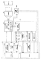
- FIG. 1 is a block diagram illustrating an optical scanning control apparatus according to the first embodiment.
- FIG. 2 is a plan view illustrating an optical scanning device constituting the optical scanning control device. (Schematic configuration of optical scanning control device)
- the optical scanning control device 1 includes a circuit unit 10, a light source unit 20, an optical scanning device 30, an optical unit 40, a screen 50, and a light amount detection sensor 60 as main components.
- the optical scanning control device 1 is, for example, a laser scanning projector.
- the circuit unit 10 is a part that controls the light source unit 20 and the optical scanning device 30, and includes, for example, a system controller 11, a CPU (Central Processing Unit) 12, a buffer circuit 13, a mirror driving circuit 14, a laser driving circuit 15, and a temperature.
- Various drive circuits such as the control circuit 16 can be used.
- the light source unit 20 includes an LD module 21, a temperature control unit 22, a temperature sensor 23, and a neutral density filter 24.
- the LD module 21 includes lasers 211R, 211G, and 211B that change the amount of light emitted according to the current value, a light amount detection sensor 215 that monitors the most recent light amounts of the lasers 211R, 211G, and 211B, and the like.
- the laser 211R is, for example, a red semiconductor laser, and can emit light having a wavelength ⁇ R (for example, 640 nm).
- the laser 211G is, for example, a green semiconductor laser, and can emit light having a wavelength ⁇ G (for example, 530 nm).
- the laser 211B is, for example, a blue semiconductor laser, and can emit light having a wavelength ⁇ B (for example, 445 nm).
- the light quantity detection sensor 215 for example, a photodiode or the like can be used.
- the light quantity detection sensor 215 can be disposed at an arbitrary position where the light quantity before passing through the neutral density filter 24 can be detected.
- the temperature control unit 22 can control the lasers 211R, 211G, and 211B to a predetermined temperature.
- the temperature sensor 23 can detect the temperatures of the lasers 211R, 211G, and 211B.
- a Peltier element can be used.
- a thermistor can be used as the temperature sensor 23.
- the neutral density filter 24 is disposed in front of the mirror 310, and the light (the combined light) emitted from the lasers 211R, 211G, and 211B is incident thereon.
- the neutral density filter 24 has a function of adjusting the luminance on the screen 50.
- an ND (Neutral Density) filter, a liquid crystal element, a polarizing filter, or the like can be used as the neutral density filter 24.
- the neutral density filter 24 is inserted, for example, inclined with respect to the optical axis of the incident light, and light that is not transmitted (light that is attenuated) is absorbed or reflected by the neutral density filter 24.
- the optical scanning device 30 is, for example, a MEMS (Micro Electro Mechanical System) that drives a mirror 310 with a piezoelectric element.
- the mirror 310 reflects the light (combined light) emitted from the lasers 211R, 211G, and 211B, scans the incident light in two dimensions in the horizontal and vertical directions according to the video signal, and couples it to the screen 50. It functions as scanning means for imaging.
- the optical scanning device 30 includes a mirror 310, a mirror support 320, torsion beams 330A and 330B, connection beams 340A and 340B, drive beams 350A and 350B, and movable.
- the drive beams 350A and 350B have drive sources 351A and 351B, respectively.
- the driving beams 370A and 370B have driving sources 371R and 371L, respectively.
- the drive beams 350A and 350B and the drive beams 370A and 370B function as actuators that scan the laser beam by swinging the mirror 310 up and down or left and right.
- a slit 322 is formed in the mirror support part 320 along the circumference of the mirror 310. The slit 322 can relieve the stress generated when the twist of the torsion beams 330A and 330B is transmitted to the mirror 310 while reducing the weight of the mirror support 320.
- the mirror 310 is supported on the surface of the mirror support 320, and the mirror support 320 is connected to the ends of the torsion beams 330A and 330B on both sides.
- the torsion beams 330A and 330B constitute a swing shaft, extend in the axial direction, and support the mirror support 320 from both sides in the axial direction.
- the mirror 310 supported by the mirror support portion 320 swings, and an operation of scanning the reflected light of the light irradiated on the mirror 310 is performed.
- the torsion beams 330A and 330B are connected and supported by the connecting beams 340A and 340B, respectively, and are connected to the driving beams 350A and 350B.
- the driving beams 350A and 350B, the connecting beams 340A and 340B, the torsion beams 330A and 330B, the mirror support 320 and the mirror 310 are surrounded by the movable frame 360.
- Each of the driving beams 350A and 350B is supported on the movable frame 360 on one side.
- the other side of the driving beam 350A extends to the inner peripheral side and is connected to the connecting beams 340A and 340B.
- the other side of the driving beam 350B extends to the inner peripheral side and is connected to the connecting beams 340A and 340B.
- the drive beams 350A and 350B are provided in a pair so as to sandwich the mirror 310 and the mirror support portion 320 in a direction orthogonal to the torsion beams 330A and 330B.
- Drive sources 351A and 351B are formed on the surfaces of the drive beams 350A and 350B, respectively.
- the driving sources 351A and 351B are piezoelectric elements having a structure in which a lower electrode, a piezoelectric film (such as a PZT film), and an upper electrode are sequentially stacked on the surfaces of the driving beams 350A and 350B.
- the driving sources 351A and 351B expand or contract according to the polarity of the driving voltage applied to the upper electrode and the lower electrode. For this reason, if drive voltages having different phases are alternately applied to the drive beam 350A and the drive beam 350B, the drive beam 350A and the drive beam 350B vibrate alternately on the left and right sides of the mirror 310 in the opposite directions. As a result, the mirror 310 can be swung around the axis with the torsion beams 330A and 330B as the swing axis or the rotation axis.
- the direction in which the mirror 310 swings around the axes of the torsion beams 330A and 330B is hereinafter referred to as the horizontal direction.
- the drive beams 350A and 350B are horizontal drive beams including the drive sources 351A and 351B that are horizontal drive sources that swing the mirror 310 in the horizontal direction.
- one end of the drive beams 370 ⁇ / b> A and 370 ⁇ / b> B is connected to the outside of the movable frame 360.
- the drive beams 370A and 370B are connected to the movable frame 360 at a point-symmetrical position about the mirror 310, and are provided in pairs so as to sandwich the movable frame 360 from both the left and right sides.
- the driving beam 370A has a zigzag shape as a whole, in which a beam extending in parallel with the driving beam 350A is connected to an adjacent beam at an end.
- the other end of the drive beam 370 ⁇ / b> A is connected to the inside of the fixed frame 380.
- the driving beam 370B has a zigzag shape as a whole, in which a beam extending in parallel with the driving beam 350B is connected to an adjacent beam at an end.
- the other end of the drive beam 370 ⁇ / b> B is connected to the inside of the fixed frame 380.
- driving sources 371R and 371L are formed for each rectangular unit not including a curved portion, respectively.
- the drive sources 371R and 371L are piezoelectric elements having a structure in which a lower electrode, a piezoelectric film, and an upper electrode are sequentially stacked on the surfaces of the drive beams 370A and 370B.
- the driving beams 370A and 370B apply the driving voltages having different polarities between the driving sources 371R and 371L adjacent to each other in a rectangular unit, thereby causing the adjacent rectangular beams to bend in the opposite directions in the vertical direction.
- the accumulated motion is transmitted to the movable frame 360. With this operation, the driving beams 370A and 370B swing the mirror 310 in a vertical direction that is a direction orthogonal to the parallel direction.
- non-resonant vibration can be used for vertical driving by the driving beams 370A and 370B.
- the drive source 371R includes drive sources 371AR, 371BR, 371CR, 371DR, 371ER, and 371FR arranged from the movable frame 360 side to the right side.
- the drive source 371L includes drive sources 371AL, 371BL, 371CL, 371DL, 371EL, and 371FL arranged from the movable frame 360 side to the left side.
- the drive sources 371AR, 371BL, 371CR, 371DL, 371ER, and 371FL are driven in the same waveform, and the drive sources 371BR, 371AL, 371DR, 371CL, 371FR, and 371EL are driven in the same waveform with different phases from the former, thereby swinging in the vertical direction.
- the drive beams 370A and 370B are vertical drive beams provided with drive sources 371R and 371L that are vertical drive sources that swing the mirror 310 in the vertical direction.
- a drive wiring for applying a drive voltage to the upper electrode and the lower electrode of the drive source 351A is connected to a predetermined terminal included in a terminal group TA provided in the fixed frame 380.
- the drive wiring for applying the drive voltage to the upper electrode and the lower electrode of the drive source 351B is connected to a predetermined terminal included in the terminal group TB provided on the fixed frame 380. Further, the drive wiring for applying the drive voltage to the upper electrode and the lower electrode of the drive source 371R is connected to a predetermined terminal included in the terminal group TA provided in the fixed frame 380. In addition, the drive wiring for applying the drive voltage to the upper electrode and the lower electrode of the drive source 371L is connected to a predetermined terminal included in the terminal group TB provided on the fixed frame 380.
- the optical scanning device 30 detects a horizontal tilt degree (horizontal swing angle) of the mirror 310 in a state where the drive voltage is applied to the drive sources 351A and 351B and the mirror 310 swings in the horizontal direction.
- a displacement sensor 391 is provided.
- Reference numerals 392, 393 and 394 denote dummy sensors.
- the optical scanning device 30 detects a vertical tilt degree (vertical swing angle) of the mirror 310 in a state where the drive voltage is applied to the drive sources 371R and 371L and the mirror 310 swings in the vertical direction.
- Displacement sensors 395 and 396 are provided.
- the optical unit 40 is an optical system for projecting the light scanned by the optical scanning device 30 onto the screen 50.
- the light incident on the optical unit 40 from the optical scanning device 30 forms an image on the screen 50, and an image corresponding to the video signal is drawn on the screen 50.
- the screen 50 includes, for example, a microlens array in order to remove noise of an image that looks grainy called speckle.
- each microlens constituting the microlens array corresponds to a pixel of the display, and the irradiated laser beam is desirably equal to or smaller than the size of the microlens.
- the light quantity detection sensor 60 can be disposed at any position where the light quantity after passing through the neutral density filter 24 can be detected.
- the light amount detection sensor 60 can independently detect the light amounts of the lasers 211R, 211G, and 211B after passing through the neutral density filter 24.
- the system controller 11 serving as a control unit generates a drive signal based on a signal obtained through the sensor wiring.
- the mirror drive circuit 14 drives the mirror 310 based on the drive signal generated by the system controller 11. More specifically, for example, the system controller 11 monitors the horizontal and vertical inclinations of the mirror 310 obtained by the horizontal displacement sensor 391 and the vertical displacement sensors 395 and 396 via the buffer circuit 13 and sends them to the mirror drive circuit 14. An angle control signal can be provided.
- the mirror drive circuit 14 supplies a predetermined drive signal to the drive beams 351 and 352 and the drive beams 371 and 372 based on the angle control signal from the system controller 11 to drive (scan) the mirror 310 at a predetermined angle. can do.
- the system controller 11 can supply, for example, a digital video signal to the laser driving circuit 15.
- the laser drive circuit 15 supplies a predetermined current to the lasers 211R, 211G, and 211B based on the video signal from the system controller 11. Accordingly, the lasers 211R, 211G, and 211B emit red, green, and blue light modulated according to the video signal, and a color image can be formed by combining these light.
- the CPU 12 can monitor the amount of light emitted from the bases of the lasers 211 R, 211 G, and 211 B based on the output of the light amount detection sensor 215 and supply a light amount control signal to the LD module 21.
- the lasers 211 ⁇ / b> R, 211 ⁇ / b> G, and 211 ⁇ / b> B are current-controlled so as to obtain a predetermined output (light quantity) based on the light quantity control signal from the CPU 12.
- the light amount detection sensor 215 can include three sensors that independently detect the light amounts emitted from the lasers 211R, 211G, and 211B. Alternatively, the light amount detection sensor 215 may be composed of only one sensor.
- the emitted light amounts of the lasers 211R, 211G, and 211B can be controlled by sequentially emitting the lasers 211R, 211G, and 211B and sequentially detecting them with one sensor.
- the CPU 12 can monitor the temperatures of the lasers 211 R, 211 G, and 211 B based on the output of the temperature sensor 23 and supply a temperature control signal to the temperature control circuit 16. Then, the temperature control circuit 16 supplies a predetermined current to the temperature control unit 22 based on the temperature control signal from the CPU 12. Thereby, the temperature control part 22 is heated or cooled, and it can control so that each laser may become predetermined
- the light quantity detection sensor 60 detects the light quantity after passing through the neutral density filter 24.
- the light amount detection sensor 215 for adjusting the light amount of each laser is mounted in the LD module 21 and is the root of the lasers 211R, 211G, and 211B (before passing through the neutral density filter 24). ) The amount of emitted light is detected.
- the image actually displayed by the optical scanning control device 1 is based on the light imaged on the screen 50, there is a case where correct adjustment cannot be performed by adjustment based on the laser light quantity at the base.
- the neutral density filter 24 is provided on the optical path, the expected attenuation ratio cannot be obtained depending on the characteristics of the neutral density filter 24. Therefore, the amount of light after passing through the neutral density filter 24 is as expected. It may not be possible.
- a light amount detection sensor 60 is provided as a light amount detection unit that detects the amount of light after passing through the neutral density filter 24.
- the detection result of the light quantity detection sensor 60 is input to the CPU 12, and the CPU 12 can supply a light quantity control signal for controlling the current value of each laser to the LD module 21 based on the light quantity detected by the light quantity detection sensor 60.
- the amount of laser light including fluctuations in the characteristics of the neutral density filter 24 can be detected, so that accurate light amount control corresponding to the image actually displayed on the screen 50 can be performed.
- the light amount detection sensor 60 can independently detect the respective light amounts of the lasers 211R, 211G, and 211B, and the CPU 12 determines the current values of the respective lasers based on the respective light amounts detected by the light amount detection sensor 60. Can be controlled. (Electrical scanning module electrical wiring) FIG.
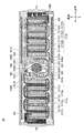
- the optical scanning module 400 includes the optical scanning device 30, a package 410, a connector 450, and a substrate 490. As described later, the optical scanning module 400 may include a package cover 420, a cover glass 430, and the like (see FIG. 8 and the like).
- the optical scanning device 30 is mounted on a package 410, and the package 410 is connected to a substrate 490 through a connector 450.
- the package 410 is, for example, a ceramic package, and laminated wiring (for example, about 10 layers of wiring) is provided in the package 410.
- the package 410 may be a printed wiring board or the like other than ceramic, and the base material is not limited as long as it can be a multilayer wiring board.
- the substrate 490 is, for example, a flexible printed circuit board.
- Sensor wiring P described later S , Drive wiring P D , And GND wiring P G Are routed from the optical scanning device 30 into the package 410 and further into the substrate 490.
- sensor signals obtained by the horizontal displacement sensor 391 and the vertical displacement sensors 395 and 396 are used. These sensor signals are used for laser emission timing, ringing control, failure detection, etc., in addition to deflection angle control.
- the sensor signals of the horizontal displacement sensor 391 and the vertical displacement sensors 395 and 396 are connected from the terminal groups TA and TB of the optical scanning device 30 to the terminal groups TC and TD of the package 410. Then, it passes through the laminated wiring in the package 410 and further passes through the wiring of the connector 450 and the substrate 490 to reach the terminal group TE.
- the horizontal drive signal and vertical drive signal for driving the mirror 310 are also wired from the terminal groups TA and TB of the optical scanning device 30 to the terminal group TE.
- a plurality of wirings are three-dimensionally arranged and electric crosstalk is likely to occur, so that a measure for preventing the occurrence of electrical crosstalk is required.
- the above electrical crosstalk strongly depends on the mutual capacitance and mutual inductance between wirings.
- Crosstalk due to mutual capacitance becomes a capacitor when adjacent wires have capacitance, and if there is a charge on one side, the charge is induced even if the wire is not directly connected, and a charge is also generated on the other wire It is a phenomenon.
- the magnitude of the crosstalk is determined by the mutual capacitance and the input voltage applied to the wiring.
- the following measures are taken for the stacked wiring of the package 410. That is, as shown in FIG. 4, in each layer of the laminated wiring, the wiring P S And wiring P D GND wiring P between G Is sandwiched between them. Also, wiring P S And wiring P D Is a GND surface (GND layer). As a result, the wiring P S And wiring P D It is possible to make it difficult to have a capacitance between the two.
- the wiring P S Is sensor wiring connected to the displacement sensor, and wiring P D Is a drive wiring through which a drive signal for swinging the mirror 310 passes (the same applies hereinafter).
- the wiring P S And wiring P D It is preferable to sandwich a GND layer LG having a GND surface between the wiring layers L1 and L2 in which the entire surface is GND. That is, it is preferable to sandwich the GND between the wirings not only in the plane direction of the wirings but also in the vertical direction. As a result, the wiring P S And wiring P D Is a GND wiring P provided between the wirings. G Then, it is surrounded by the GND surface provided in the lower GND layer LG, and it is difficult to have a capacitance. In the above description, the entire surface of the GND layer LG is the GND layer, but the wiring P is directly below the wirings of the wiring layers L1 and L2.
- Crosstalk due to mutual inductance is a phenomenon in which a magnetic field is generated by electromagnetic induction due to a temporal change in current flowing through each wiring, and an electromotive force is generated by the magnetic field.
- the magnitude of the crosstalk is determined by the temporal change amount of the current and the current amount. Therefore, in this embodiment, in order to suppress (reduce) the crosstalk due to the mutual inductance, the following measures are taken for the laminated wiring of the package 410. That is, as shown in the plan view of FIG. 5A, in each layer of the laminated wiring, the wiring P arranged in an arbitrary layer.
- Wiring P S And wiring P S Wiring P arranged in a layer adjacent to the upper side or lower side of D are arranged so as not to overlap in plan view.
- Wiring P S And wiring P D When viewed from above, the distance L is preferably at least one wire (for example, 0.05 mm or more), and the distance L is preferably as far as possible.
- the wiring P arranged in an arbitrary layer S And wiring P S Wiring P arranged in a layer adjacent to the upper side or lower side of D Can be arranged so that portions extending in substantially the same direction do not overlap in plan view.
- wiring P S And wiring P D May have a portion that partially intersects in plan view.
- FIG. 5B shows such an example. Wiring P shown in FIG.
- S And wiring P D Is arranged so as not to overlap in a plan view in a portion extending in substantially the same direction (a portion extending in the horizontal direction in the figure). However, it includes locations that intersect in plan view. In this way, as shown in the plan view of FIG. S And wiring P D ) Intersect, it is preferable to make the crossing angle as orthogonal as possible without making the crossing angle an acute angle. This is to reduce the generation of electromotive force due to electromagnetic induction. Also, wiring P S And wiring P D Are arranged in the same layer, the wiring P S And wiring P D Are preferably not parallel. Also, wiring P S And wiring P D Even when the wires are arranged in different layers, the wiring P S And wiring P D Are preferably not parallel.
- FIGS. 7A and 7B show a conventional package
- FIG. 7B shows a package 410.
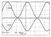
- the waveform of V_SENS is in phase with the waveform of V_DRV. Due to the structure of the optical scanning device 30, the V_SENS waveform and the V_DRV waveform should be reversed in phase by 180 degrees.
- V_SENS waveform and the V_DRV waveform are inverted in phase by 180 degrees as theoretically, and the original sensor waveform reflecting the driving state of the mirror 310 is reflected in V_SENS. It can be seen that is output.
- the optical scanning module 400 when the sensor wiring and the driving wiring are laminated, the sensor wiring and the driving wiring are arranged so as not to overlap in a plan view. When the sensor wiring and the driving wiring are wired in the same layer, a GND wiring is provided between the adjacent sensor wiring and the driving wiring.
- the optical scanning module 400 when the sensor wiring and the driving wiring are laminated, it is preferable that the GND wiring is provided between the sensor wiring and the driving wiring adjacent to each other in the vertical direction. In addition, when the sensor wiring and the driving wiring adjacent in the vertical direction intersect with each other, it is preferable to arrange them so that they are orthogonal to each other. As a result, crosstalk generated between the sensor wiring and the drive wiring can be further reduced, and a signal from the sensor wiring can be detected more accurately.
- GND wiring is provided between the sensor wiring and the driving wiring adjacent to each other in the vertical direction.
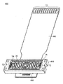
- FIG. 8 is a perspective view (part 1) for explaining GND reinforcement of a package.
- a package cover 420 is provided on the package 410 so as to cover the optical scanning device 30.
- the optical scanning device 30 is covered with the package cover 420 and cannot be visually recognized.
- An opening that exposes the vicinity of the mirror 310 of the optical scanning device 30 is provided at a substantially central portion of the package cover 420, and a cover glass 430 that transmits incident light and outgoing light is provided so as to cover the opening. Yes.
- the GND wiring P is provided at a position exposed from the package cover 420 at the outer edge of the surface of the package 410 on the side where the optical scanning device 30 is mounted.
- G Is provided, and external connection is possible.
- GND wiring P G Are routed from the GND wiring in the package 410 to the surface of the package 410.
- the GND wiring P G One or a plurality may be provided, but here, as an example, one is provided at each of the four corners of the surface of the package 410 on the side where the optical scanning device 30 is mounted.
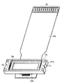
- 9A and 9B are perspective views (No. 2) for explaining the GND strengthening of the package. As shown in FIG. 9A, the package 410 includes a GND wiring P.
- FIG. 9B shows a state in which the package 410 is attached to the housing 600 (not shown in FIG. 9B).
- the hold pin 700 has a structure in which a small-diameter columnar portion is provided substantially concentrically at the tip of a large-diameter columnar portion.
- the side surface of the large-diameter columnar portion of the hold pin 700 is brought into contact with the substantially V-shaped groove 410x provided on the side surface of the package 410, so that the small-diameter columnar portion. Is inserted into a hole provided in the housing 600 and fixed. At this time, by adjusting the position of the package 410 with respect to the housing 600 (that is, adjusting the position of the mirror 310) by making the hole larger and moving the position of the hold pin 700 left and right.
- the housing 600 is made of a metal or an insulator whose surface is coated with a metal, and has a GND potential.
- the package cover 420 is provided with a deaeration port 420x, and the deaeration port 420x is filled with an ultraviolet curable resin or the like and closed.
- FIG. 10A the package cover 420 is provided with a deaeration port 420x, and the deaeration port 420x is filled with an ultraviolet curable resin or the like and closed.
- FIG. 10B shows an enlarged view of the deaeration port 420x before being filled with the ultraviolet curable resin or the like.
- the reason for providing the deaeration port 420x is as follows.
- the structure of FIG. 10A can be produced, for example, by bonding the cover glass 430 to the package cover 420 and then curing the package cover 420 including the cover glass 430 to the package 410 with a thermosetting adhesive.
- the thermosetting adhesive when cured with the thermosetting adhesive, the gas in the sealed space sealed by the package cover 420 and the package 410 provided with the cover glass 430 expands, and the adhesive is in a state where the package cover 420 is lifted. There is a risk of curing.
- the deaeration opening 420x is closed again with an ultraviolet curable resin or the like at room temperature, so that the package cover 420 can be reliably sealed without being floated.
- the preferred embodiment has been described in detail above.
- the present invention is not limited to the above-described embodiment, and various modifications and replacements are made to the above-described embodiment without departing from the scope described in the claims. Can be added.
- the optical scanning control device according to the present invention is applied to a laser scanning projector has been described.
- this is merely an example, and the optical scanning control device according to the present invention can be applied to various devices that display images on a screen.
- Examples of such devices include a vehicle-mounted head-up display, head-mounted display, laser printer, laser scanning epilator, laser head lamp, and laser radar.
- Optical scanning control apparatus 10 Circuit part 11 System controller 12 CPU DESCRIPTION OF SYMBOLS 13 Buffer circuit 14 Mirror drive circuit 15 Laser drive circuit 16 Temperature control circuit 20 Light source part 21 LD module 22 Temperature control part 23 Temperature sensor 24 Neutral filter 30 Optical scanning device 40 Optical part 50 Screen 60 Light quantity detection sensor 211R, 211G, 211B Laser 215 Light quantity detection sensor 310 Mirror 320 Mirror support part 322 Slit 330A, 330B Twist beam 340A, 340B Connection beam 350A, 350B, 370A, 370B Drive beam 351A, 351B, 371R, 371L Drive source 360 Movable frame 380 Fixed frame 391 Horizontal displacement Sensor 392, 393, 394 Dummy sensor 395, 396 Vertical displacement sensor 400 Optical scanning module 410 Package 410x Groove 420 Package cover 420x Deaeration port 43 0 Cover glass 450 Connector 490 Substrate 600 Case 700 Hold pin
Abstract
The purpose of the present invention is to provide an optical scanning module capable of reducing crosstalk between sensor wires and drive wires. This optical scanning module is equipped with an optical scanning device which scans incident light by oscillating a mirror, and a package in which the optical scanning device is installed. The optical scanning device is provided with displacement sensors that detect the oscillation angle of the mirror. Sensor wires (PS) connected to the displacement sensors and drive wires over which travels a drive signal for oscillating the mirror are led into the package from the optical scanning device. Wiring layers (L1, L2) having the sensor wires and the drive wires (PD) formed thereon are stacked. The sensor wires and drive wires are disposed so as not to overlap in plan view of the layers. With regard to a sensor wire and a drive wire in the same wiring layer, a GND wire (PG) is provided between the adjacent sensor wire and drive wire.
Description
本発明は、光走査モジュール、及び光走査制御装置に関する。
The present invention relates to an optical scanning module and an optical scanning control device.
従来、ミラーを回転軸回りに回転させてレーザ光等の入射光を反射させる光走査装置をパッケージに搭載した光走査モジュールが知られている。この光走査モジュールには、ミラーが駆動され揺動している状態でミラーの振角を検出する変位センサが設けられており、変位センサの出力する信号に基づいてミラーの傾きが検出されミラーが駆動制御される(例えば、特許文献1参照)。
Conventionally, there has been known an optical scanning module in which an optical scanning device for reflecting incident light such as laser light by rotating a mirror around a rotation axis is mounted on a package. The optical scanning module is provided with a displacement sensor that detects the swing angle of the mirror while the mirror is driven and oscillated, and the mirror tilt is detected based on a signal output from the displacement sensor. The drive is controlled (for example, see Patent Document 1).
しかしながら、上記の光走査モジュールにおいて、変位センサに接続されるセンサ配線と、ミラーを揺動させる駆動信号が通る駆動配線とは、パッケージ内等で複雑に引き回される場合があり、引き回し方によっては、センサ配線と駆動配線との間にクロストークが生じ、センサ配線からの信号を正確に検出できないおそれがある。
本発明は、上記の点に鑑みてなされたもので、センサ配線と駆動配線との間に生じるクロストークを低減可能な光走査モジュールを提供することを課題とする。 However, in the above optical scanning module, the sensor wiring connected to the displacement sensor and the driving wiring through which the driving signal for swinging the mirror passes may be complicatedly routed in a package or the like. In this case, crosstalk occurs between the sensor wiring and the drive wiring, and there is a possibility that the signal from the sensor wiring cannot be detected accurately.
The present invention has been made in view of the above points, and an object of the present invention is to provide an optical scanning module capable of reducing crosstalk generated between a sensor wiring and a driving wiring.
本光走査モジュール(400)は、ミラー(310)を揺動させて入射光を走査する光走査装置(30)と、前記光走査装置(30)を搭載するパッケージ(410)と、を備えた光走査モジュール(400)であって、前記光走査装置(30)は、前記ミラー(310)の振角を検出する変位センサ(391、395、396)を有し、前記変位センサ(391、395、396)に接続されるセンサ配線(PS)、及び前記ミラー(310)を揺動させる駆動信号が通る駆動配線(PD)が前記光走査装置(30)から前記パッケージ(410)内に引き回され、前記センサ配線(PS)と前記駆動配線(PD)とが形成される配線層は積層され、前記センサ配線(PS)と前記駆動配線(PD)とが各層の平面視において重複しないように配置され、同一配線層内の前記センサ配線(PS)と前記駆動配線(PD)とは、隣接する前記センサ配線(PS)と前記駆動配線(PD)との間にGND配線(PG)が設けられることを要件とする。
なお、上記括弧内の参照符号は、理解を容易にするために付したものであり、一例にすぎず、図示の態様に限定されるものではない。 The optical scanning module (400) includes an optical scanning device (30) that scans incident light by swinging a mirror (310), and a package (410) that mounts the optical scanning device (30). It is an optical scanning module (400), Comprising: The said optical scanning device (30) has the displacement sensor (391,395,396) which detects the swing angle of the said mirror (310), The said displacement sensor (391,395) 396) is connected to the sensor wiring (P S ) and the driving wiring (P D ) through which the driving signal for swinging the mirror (310) passes from the optical scanning device (30) into the package (410). The wiring layers that are routed to form the sensor wiring (P S ) and the driving wiring (P D ) are stacked, and the sensor wiring (P S ) and the driving wiring (P D ) are planar surfaces of each layer. Duplicate in vision Are arranged so as not, the said sensor wires in the same wiring layer (P S) and said drive line (P D), between adjacent said sensor wire (P S) and said drive line (P D) It is a requirement that a GND wiring (P G ) is provided.
Note that the reference numerals in the parentheses are given for ease of understanding, are merely examples, and are not limited to the illustrated modes.
開示の技術によれば、センサ配線と駆動配線との間に生じるクロストークを低減可能な光走査モジュールを提供できる。
According to the disclosed technology, it is possible to provide an optical scanning module capable of reducing crosstalk generated between the sensor wiring and the drive wiring.
以下、図面を参照して発明を実施するための形態について説明する。各図面において、同一構成部分には同一符号を付し、重複した説明を省略する場合がある。
〈第1の実施の形態〉
図1は、第1の実施の形態に係る光走査制御装置を例示するブロック図である。図2は、光走査制御装置を構成する光走査装置を例示する平面図である。
(光走査制御装置の概略構成)
まず、図1及び図2を参照して、光走査制御装置1の概略構成について説明する。光走査制御装置1は、主要な構成要素として、回路部10と、光源部20と、光走査装置30と、光学部40と、スクリーン50と、光量検出センサ60とを有する。光走査制御装置1は、例えば、レーザ走査型プロジェクタである。
回路部10は、光源部20や光走査装置30を制御する部分であり、例えば、システムコントローラ11やCPU(Central Processing Unit)12、並びにバッファ回路13、ミラー駆動回路14、レーザ駆動回路15、温度制御回路16等の各種駆動回路等により構成することができる。
光源部20は、LDモジュール21と、温度制御部22と、温度センサ23と、減光フィルタ24とを有する。
LDモジュール21は、電流値に応じて出射する光量が変化するレーザ211R、211G、及び211Bや、レーザ211R、211G、及び211Bの夫々の直近の光量をモニタする光量検出センサ215等を備えている。レーザ211Rは、例えば、赤色半導体レーザであり、波長λR(例えば、640nm)の光を出射することができる。レーザ211Gは、例えば、緑色半導体レーザであり、波長λG(例えば、530nm)の光を出射することができる。レーザ211Bは、例えば、青色半導体レーザであり、波長λB(例えば、445nm)の光を出射することができる。光量検出センサ215としては、例えば、フォトダイオード等を用いることができる。光量検出センサ215は、減光フィルタ24を通過前の光量を検出できる任意の位置に配置することができる。
温度制御部22は、レーザ211R、211G、及び211Bを所定の温度に制御することができる。温度センサ23は、レーザ211R、211G、及び211Bの夫々の温度を検出することができる。温度制御部22としては、例えば、ペルチェ素子を用いることができる。温度センサ23としては、例えば、サーミスタを用いることができる。
減光フィルタ24は、ミラー310の前段に配置され、レーザ211R、211G、及び211Bから出射された光(合成後の光)が入射する。減光フィルタ24は、スクリーン50上の輝度を調整する機能を有する。減光フィルタ24としては、ND(Neutral Density)フィルタや液晶素子、偏光フィルタ等を用いることができる。減光フィルタ24は、例えば、入射光の光軸に対して傾けて挿入され、透過しない光(減光される光)は、減光フィルタ24によって吸収若しくは反射される。
光走査装置30は、例えば、圧電素子によりミラー310を駆動させるMEMS(Micro Electro Mechanical System)である。ミラー310は、レーザ211R、211G、及び211Bから出射された光(合成後の光)を反射させ、映像信号に応じて入射光を水平方向及び垂直方向の2次元に走査してスクリーン50に結像させる走査手段として機能する。
具体的には、図2に示すように、光走査装置30は、ミラー310と、ミラー支持部320と、捻れ梁330A及び330Bと、連結梁340A及び340Bと、駆動梁350A及び350Bと、可動枠360と、駆動梁370A及び370Bと、固定枠380とを有する。又、駆動梁350A及び350Bは、それぞれ駆動源351A及び351Bを有する。又、駆動梁370A及び370Bは、それぞれ駆動源371R及び371Lを有する。駆動梁350A及び350B、駆動梁370A及び370Bは、ミラー310を上下又は左右に揺動してレーザ光を走査するアクチュエータとして機能する。
ミラー支持部320には、ミラー310の円周に沿うようにスリット322が形成されている。スリット322により、ミラー支持部320を軽量化しつつ捻れ梁330A及び330Bによる捻れをミラー310へ伝達する際に発生する応力を緩和することができる。
光走査装置30において、ミラー支持部320の表面にミラー310が支持され、ミラー支持部320は、両側にある捻れ梁330A及び330Bの端部に連結されている。捻れ梁330A及び330Bは、揺動軸を構成し、軸方向に延在してミラー支持部320を軸方向両側から支持している。捻れ梁330A及び330Bが捻れることにより、ミラー支持部320に支持されたミラー310が揺動し、ミラー310に照射された光の反射光を走査させる動作を行う。捻れ梁330A及び330Bは、それぞれが連結梁340A及び340Bに連結支持され、駆動梁350A及び350Bに連結されている。
駆動梁350A及び350B、連結梁340A及び340B、捻れ梁330A及び330B、ミラー支持部320及びミラー310は、可動枠360に取り囲まれている。駆動梁350A及び350Bは、可動枠360にそれぞれの一方の側が支持されている。駆動梁350Aの他方の側は内周側に延びて連結梁340A及び340Bと連結している。駆動梁350Bの他方の側も同様に、内周側に延びて連結梁340A及び340Bと連結している。
駆動梁350A及び350Bは、捻れ梁330A及び330Bと直交する方向に、ミラー310及びミラー支持部320を挟むように、対をなして設けられている。駆動梁350A及び350Bの表面には、駆動源351A及び351Bがそれぞれ形成されている。駆動源351A及び351Bは、駆動梁350A及び350Bの表面上に下部電極、圧電膜(PZT膜等)、及び上部電極が順次積層された構造の圧電素子である。駆動源351A及び351Bは、上部電極と下部電極に印加する駆動電圧の極性に応じて伸長したり縮小したりする。
このため、駆動梁350Aと駆動梁350Bとで異なる位相の駆動電圧を交互に印加すれば、ミラー310の左側と右側で駆動梁350Aと駆動梁350Bとが上下反対側に交互に振動する。これにより、捻れ梁330A及び330Bを揺動軸又は回転軸として、ミラー310を軸周りに揺動させることができる。ミラー310が捻れ梁330A及び330Bの軸周りに揺動する方向を、以後、水平方向と呼ぶ。例えば駆動粱350A及び350Bによる水平駆動には、共振振動が用いられ、高速にミラー310を揺動駆動することができる。
このように、駆動梁350A及び350Bは、ミラー310を水平方向に揺動する水平駆動源である駆動源351A及び351Bを備えた水平駆動梁である。
又、可動枠360の外部には、駆動梁370A及び370Bの一端が連結されている。駆動梁370A及び370Bは、ミラー310を中心として点対称な位置で可動枠360と連結され、可動枠360を左右両側から挟むように、対をなして設けられている。駆動梁370Aは、駆動梁350Aと平行に延在する梁が、隣接する梁と端部で連結され、全体としてジグザグ状の形状を有する。そして、駆動梁370Aの他端は、固定枠380の内側に連結されている。駆動梁370Bも同様に、駆動梁350Bと平行に延在する梁が、隣接する梁と端部で連結され、全体としてジグザグ状の形状を有する。そして駆動梁370Bの他端は、固定枠380の内側に連結されている。
駆動梁370A及び370Bの表面には、それぞれ曲線部を含まない矩形単位毎に駆動源371R及び371Lが形成されている。駆動源371R及び371Lは、駆動梁370A及び370Bの表面上に下部電極、圧電膜、及び上部電極が順次積層された構造の圧電素子である。
駆動梁370A及び370Bは、矩形単位毎に隣接している駆動源371R及び371L同士で、異なる極性の駆動電圧を印加することにより、隣接する矩形梁を上下反対方向に反らせ、各矩形梁の上下動の蓄積を可動枠360に伝達する。駆動梁370A及び370Bは、この動作により、平行方向と直交する方向である垂直方向にミラー310を揺動させる。例えば駆動梁370A及び370Bによる垂直駆動には、非共振振動を用いることができる。
例えば、駆動源371Rは、可動枠360側から右側に向かって並ぶ駆動源371AR、371BR、371CR、371DR、371ER及び371FRを含む。又、駆動源371Lは、可動枠360側から左側に向かって並ぶ駆動源371AL、371BL、371CL、371DL、371EL及び371FLを含む。この場合、駆動源371AR、371BL、371CR、371DL、371ER、371FLを同波形、駆動源371BR、371AL、371DR、371CL、371FR、371ELを前者と位相の異なる同波形で駆動することで垂直方向へ揺動することができる。
このように、駆動梁370A及び370Bは、ミラー310を垂直方向に揺動する垂直駆動源である駆動源371R及び371Lを備えた垂直駆動梁である。
駆動源351Aの上部電極及び下部電極に駆動電圧を印加する駆動配線は、固定枠380に設けられた端子群TAに含まれる所定の端子と接続されている。又、駆動源351Bの上部電極及び下部電極に駆動電圧を印加する駆動配線は、固定枠380に設けられた端子群TBに含まれる所定の端子と接続されている。又、駆動源371Rの上部電極及び下部電極に駆動電圧を印加する駆動配線は、固定枠380に設けられた端子群TAに含まれる所定の端子と接続されている。又、駆動源371Lの上部電極及び下部電極に駆動電圧を印加する駆動配線は、固定枠380に設けられた端子群TBに含まれる所定の端子と接続されている。
光走査装置30は、駆動源351A及び351Bに駆動電圧が印加されてミラー310が水平方向に揺動している状態におけるミラー310の水平方向の傾き具合(水平方向の振角)を検出する水平変位センサ391を備えている。392、393及び394はダミーセンサである。
光走査装置30は、駆動源371R及び371Lに駆動電圧が印加されてミラー310が垂直方向に揺動している状態におけるミラー310の垂直方向の傾き具合(垂直方向の振角)を検出する垂直変位センサ395及び396を備えている。
図1に戻り、光学部40は、光走査装置30に走査された光をスクリーン50に投射するための光学系である。光走査装置30から光学部40に入射した光は、スクリーン50に結像し、スクリーン50に映像信号に応じた画像が描画される。
スクリーン50は、スペックルと呼ばれる粒状に見える画像のノイズを除去するため、例えば、マイクロレンズアレイを備えている。この場合、マイクロレンズアレイを構成する各マイクロレンズは、ディスプレイの画素に相当し、照射されるレーザビームはマイクロレンズのサイズに比べて等しいか、より小さいことが望ましい。
光量検出センサ60は、減光フィルタ24を通過後の光量を検出できる任意の位置に配置することができる。光量検出センサ60は、減光フィルタ24を通過後のレーザ211R、211G、及び211Bの夫々の光量を独立に検出可能である。光量検出センサ60としては、例えば、1つ又は複数のフォトダイオード等を用いることができる。
(光走査制御装置の概略動作)
次に、光走査制御装置1の概略動作について説明する。制御手段であるシステムコントローラ11は、例えば、センサ配線を通して得られた信号に基づいて駆動信号を生成する。ミラー駆動回路14は、例えば、システムコントローラ11が生成した駆動信号に基づいてミラー310を駆動する。
より詳しくは、システムコントローラ11は、例えば、水平変位センサ391、垂直変位センサ395及び396で得られるミラー310の水平方向及び垂直方向の傾きをバッファ回路13を介してモニタし、ミラー駆動回路14に角度制御信号を供給することができる。そして、ミラー駆動回路14は、システムコントローラ11からの角度制御信号に基づいて、駆動梁351及び352、駆動梁371及び372に所定の駆動信号を供給し、ミラー310を所定角度に駆動(走査)することができる。
又、システムコントローラ11は、例えば、ディジタルの映像信号をレーザ駆動回路15に供給することができる。そして、レーザ駆動回路15は、システムコントローラ11からの映像信号に基づいて、レーザ211R、211G、及び211Bに所定の電流を供給する。これにより、レーザ211R、211G、及び211Bが映像信号に応じて変調された赤色、緑色、及び青色の光を発し、これらを合成することでカラーの画像を形成することができる。
CPU12は、例えば、レーザ211R、211G、及び211Bの根元の出射光量を光量検出センサ215の出力によりモニタし、LDモジュール21に光量制御信号を供給することができる。レーザ211R、211G、及び211Bは、CPU12からの光量制御信号に基づいて、所定の出力(光量)になるように電流制御される。
なお、光量検出センサ215は、レーザ211R、211G、及び211Bの出射光量を独立に検出する3つのセンサを含む構成とすることができる。或いは、光量検出センサ215は、1つのセンサのみから構成してもよい。この場合には、レーザ211R、211G、及び211Bを順次発光させて、1つのセンサで順次検出することで、レーザ211R、211G、及び211Bの出射光量の制御が可能となる。
又、CPU12は、レーザ211R、211G、及び211Bの温度を温度センサ23の出力によりモニタし、温度制御回路16に温度制御信号を供給することができる。そして、温度制御回路16は、CPU12から温度制御信号に基づいて、温度制御部22に所定の電流を供給する。これにより、温度制御部22が加熱又は冷却され、各レーザが所定の温度になるように制御することができる。
光量検出センサ60は、減光フィルタ24を通過後の光量を検出する。前述のように、各レーザの光量調整を実施するための光量検出センサ215はLDモジュール21の中に実装されており、レーザ211R、211G、及び211Bの根元の(減光フィルタ24を通過前の)出射光量を検出している。しかしながら、光走査制御装置1で実際に表示される画像はスクリーン50に結像した光によるので、根元のレーザ光量による調整では正しい調整ができない場合がある。
例えば、光路上に減光フィルタ24を設けているので、減光フィルタ24の特性によっては、期待通りの減光比が得られないことから、減光フィルタ24を通過後の光量が期待通りにならない場合がある。又、減光フィルタ24のR/G/B夫々の減光比にばらつきがある場合に至っては、減光フィルタ24を通過後のホワイトバランスが崩れてしまうおそれがある。又、温度や経年劣化により、光走査装置30の特性が変動する場合もある。このような問題は、光量検出センサ215により、光走査装置30を通過前の光量を如何に精密に制御しても解決することはできない。
そこで、光走査制御装置1では、減光フィルタ24を通過後の光量を検出する光量検出手段として、光量検出センサ60を設けている。光量検出センサ60の検出結果はCPU12に入力され、CPU12は光量検出センサ60で検出した光量に基づいて、各レーザの電流値を制御する光量制御信号をLDモジュール21に供給することができる。
これにより、減光フィルタ24の特性の変動を含めたレーザ光の光量を検出できるため、スクリーン50に実際に表示される画像に対応した正確な光量制御を行うことが可能となる。なお、光量検出センサ60は、レーザ211R、211G、及び211Bの夫々の光量を独立に検出可能であり、CPU12は、光量検出センサ60で検出した夫々の光量に基づいて、夫々のレーザの電流値を制御すことができる。
(光走査モジュールの電気配線)
図3は、光走査モジュールの電気配線について説明する斜視図である。図3に示すように、光走査モジュール400は、光走査装置30と、パッケージ410と、コネクタ450と、基板490とを有している。光走査モジュール400は、後述のように、パッケージカバー420やカバーガラス430等を有していてもよい(図8等参照)。
光走査モジュール400において、光走査装置30はパッケージ410に搭載され、パッケージ410はコネクタ450を介して基板490に接続されている。パッケージ410は、例えば、セラミックパッケージであり、パッケージ410内には積層配線(例えば、10層程度の配線)が設けられている。なお、パッケージ410はセラミック以外の例えばプリント配線基板等でも良く、多層配線基板とできるものであれば基材は限定されない。
基板490は、例えば、フレキシブルプリント基板である。後述のセンサ配線PS、駆動配線PD、及びGND配線PGは、光走査装置30からパッケージ410内に引き回され、更に基板490内に引き回されている。
前述のように、システムコントローラ11がミラー310の振れ角制御を行う際に、水平変位センサ391、垂直変位センサ395及び396で得られるセンサ信号を用いる。又、これらのセンサ信号は、振れ角制御以外に、レーザの発光タイミング、リンギング制御、故障検出等に利用している。これら各制御を行うためには、水平変位センサ391、垂直変位センサ395及び396のセンサ信号を正確に検出することが重要となる。
水平変位センサ391、垂直変位センサ395及び396のセンサ信号は光走査装置30の端子群TA及びTBからパッケージ410の端子群TC及びTDに接続されている。そして、パッケージ410内の積層配線を通り、更にコネクタ450及び基板490の配線を通り端子群TEに至る。又、ミラー310を駆動する水平駆動信号と垂直駆動信号も、センサ信号と同様に、光走査装置30の端子群TA及びTBから端子群TEに配線されている。
光走査装置30から端子群TEに至る配線中で、配線間の電気的クロストークが発生するとセンサ信号を正確に検出できなくなる。特に、水平駆動信号と水平変位センサ391との間、垂直駆動信号と垂直変位センサ395及び396との間でクロストークが発生すると、センサ出力からは本来のセンサ出力とクロストークによる信号出力が同一波形、同一周波数で同時に検出される。
そのため、ミラー310が故障し振れなくなっても電気的に断線していなければセンサ出力が検出されてしまう等の不具合が発生するおそれがある。特に積層配線を有するパッケージ410では、複数の配線が立体的に配置され電気的クロストークが発生し易いため、電気的クロストークの発生を防止する対策が必要となる。
上記の電気的クロストークは、配線間の相互キャパシタンスと相互インダクタンスに強く依存する。
相互キャパシタンスによるクロストークは、近接した配線同士が静電容量を持つとコンデンサとなり、一方に電荷があると線が直接接続されていなくても電荷が誘導され、もう一方の配線にも電荷が生じる現象である。この場合、クロストークの大きさは、相互静電容量と配線に印加した入力電圧によって決定される。そこで、本実施の形態では、相互キャパシタンスによるクロストークを抑制(低減)するために、パッケージ410の積層配線に関し、以下の対応を行っている。
すなわち、図4に示すように、積層配線の各層において、配線PSと配線PDとの間にGND配線PGを挟むようにしている。又、配線PSと配線PDの周囲をGND面(GND層)としている。これにより、配線PSと配線PDとの間に静電容量を持たせ難くすることができる。なお、図4において、配線PSは変位センサに接続されるセンサ配線であり、配線PDはミラー310を揺動させる駆動信号が通る駆動配線である(以降同様)。
又、積層配線の各層において、配線PSと配線PDとが形成されている配線層L1、L2の間に全面をGNDとしたGND面を有するGND層LGを挟むことが好ましい。つまり、配線の平面方向のみならず、垂直方向に関しても配線間にGNDを挟むことが好ましい。これにより、配線PSと配線PDとは、配線間に設けられたGND配線PGと、下層のGND層LGに設けられたGND面によって囲われることとなり、静電容量を持たせ難くすることができる。なお、上述ではGND層LGの一層全面をGND層としたが、配線層L1、L2の配線の真下に配線PS、PDに沿うようにしてGND配線PGを設けてもよい。つまり、GND配線PGは面状でなく、線状としてもよい。
相互インダクタンスによるクロストークは、各配線に流れる電流が時間的に変化することで電磁誘導により磁場が発生し、更にその磁場により起電力が生じる現象である。この場合、クロストークの大きさは、電流の時間的変化量と電流量によって決定される。そこで、本実施の形態では、相互インダクタンスによるクロストークを抑制(低減)するために、パッケージ410の積層配線に関し、以下の対応を行っている。
すなわち、図5Aの平面図に示すように、積層配線の各層において、任意の層に配置された配線PSと、配線PSの上側又は下側に隣接する層に配置された配線PDとが、平面視において重複しないように配置している。配線PSと配線PDとを平面視した場合の距離Lは、最低でも配線1本分以上(例えば、0.05mm以上)とし、可能な限り距離Lを離すことが好ましい。
なお、任意の層に配置された配線PSと、配線PSの上側又は下側に隣接する層に配置された配線PDとは、略同一方向に延在する部分が、平面視において重複しないように配置することができる。ただし、配線PSと配線PDとは、平面視において部分的に交差する箇所を有してもよい。図5Bはこのような例を示す。図5Bに示した配線PSと配線PDとは、略同一方向に延在する部分(図中横方向に延在する部分)では平面視において重複しないように配置されている。ただし、平面視において交差する箇所を含む。
このように、図5Bの平面図に示すように、配線同士(配線PSと配線PD)が交差する場合は、交差角を鋭角にせず、できる限り直交させることが好ましい。電磁誘導による起電力の発生を低減するためである。又、配線PSと配線PDが同一層に配置される場合には、配線PSと配線PDとを平行にしないことが好ましい。又、配線PSと配線PDが異なる層に配置される場合にも、配線PSと配線PDとを平行にしないことが好ましい。
以上、図4、図5A及び図5Bでは、パッケージ410の積層配線について説明したが、基板490の配線についても同様の対応をすることが好ましい。クロストークを一層低減するためである。
(クロストークの検討)
次に、図3~図5Bを用いて説明したクロストークの抑制についての検討を行った。なお、ここでは、水平センサ信号をH_SENS、垂直センサ信号をV_SENS、水平駆動信号をH_DRV、垂直駆動信号をV_DRVと称する。
具体的には、H_DRVとH_SENSとの間、H_DRVとV_SENSとの間、V_DRVとH_SENSとの間、V_DRVとV_SENSとの間について、相互キャパシタンス及び相互インダクタンスのシミュレーションを行った。結果を表1及び表2に示す。
なお、パッケージ410では図4、図5A及び図5Bを考慮した配線設計がなされており、従来パッケージでは図4、図5A及び図5Bを考慮した配線設計がなされていない(以降同様)。つまり、従来パッケージでは、各層内の配線間や上下層間にGNDが設けられていなく、上下層間で配線が重なっている部分や鋭角に交差している部分が存在している。


表1及び表2に示すように、パンケージ410では、従来パッケージに比べて、相互キャパシタンス及び相互インダクタンスが低減していることがわかる。特に、相互キャパシタンスは大幅に低減している。
次に、図6のように、パッケージ410に光走査装置30が搭載されていない状態で、H_DRVに所定電圧を印加した場合のH_SENSへのクロストーク、V_DRVに所定電圧を印加した場合のV_SENSへのクロストークを実測した。結果を表3に示す。

表3に示すように、パッケージ410では、従来パッケージに比べて、水平側で75%、垂直側で84%のクロストーク改善が確認できた。
次に、図3のようにパッケージ410に光走査装置30が搭載された状態で、H_DRVに所定電圧を印加した場合のH_SENSへのクロストーク、V_DRVに所定電圧を印加した場合のV_SENSへのクロストークを実測した。結果を図7A及び図7Bに示す。なお、図7Aが従来パッケージ、図7Bがパッケージ410である。
図7Aに示すように、従来パッケージでは、V_SENSの波形がV_DRVの波形と同位相になっている。光走査装置30の構造上、本来であれば、V_SENSの波形とV_DRVの波形とは位相が180度反転するはずであるが、V_DRVからV_SENSへのクロストークが大きいため同位相となっている。
これに対して、図7Bに示すように、パッケージ410では、V_SENSの波形とV_DRVの波形とは理論通りに位相が180度反転し、V_SENSにはミラー310の駆動状態を反映した本来のセンサ波形が出力されていることがわかる。
このように、光走査モジュール400では、センサ配線と駆動配線とが積層配線される場合には、センサ配線と駆動配線とが平面視において重複しないように配置される。又、センサ配線と駆動配線とが同一層内に配線される場合には、隣接するセンサ配線と駆動配線との間にGND配線が設けられる。これらにより、センサ配線と駆動配線との間に生じるクロストークを低減することが可能となり、センサ配線からの信号を正確に検出することができる。
又、光走査モジュール400において、センサ配線と駆動配線とが積層配線される場合には、上下に隣接するセンサ配線と駆動配線との間にGND配線が設けられることが好ましい。又、上下に隣接するセンサ配線と駆動配線とが交差する場合には、両者が直交するように配置することが好ましい。これにより、センサ配線と駆動配線との間に生じるクロストークを一層低減することが可能となり、センサ配線からの信号を一層正確に検出することができる。
〈第2の実施の形態〉
第2の実施の形態では、GNDを強化する例を示す。なお、第2の実施の形態において、既に説明した実施の形態と同一構成部についての説明は省略する場合がある。
図8は、パッケージのGND強化について説明する斜視図(その1)である。図8に示すように、光走査モジュール400において、光走査装置30を覆うように、パッケージ410上にパッケージカバー420が設けられている。なお、図8では、光走査装置30はパッケージカバー420に覆われているため、視認できない。
パッケージカバー420の略中央部には光走査装置30のミラー310の近傍を露出する開口部が設けられており、開口部を覆うように入射光及び出射光を透過するカバーガラス430が設けられている。
又、パッケージ410の光走査装置30を搭載する側の表面の外縁部において、パッケージカバー420から露出する位置に、GND配線PGが設けられ、外部接続可能とされている。GND配線PGは、パッケージ410内のGND配線からパッケージ410の表面に引き回されている。なお、GND配線PGの個数は1つでも複数でもよいが、ここでは一例として、パッケージ410の光走査装置30を搭載する側の表面の4隅に1つずつ設けている。
図9A及び図9Bは、パッケージのGND強化について説明する斜視図(その2)である。図9Aに示すように、パッケージ410は、GND配線PG側を筐体600側に向けて、ホールドピン700(固定部材)により筐体600に固定されている。なお、カバーガラス430を備えたパッケージカバー420は、筐体600に設けられた開口部から反対面側に露出しており、光走査装置30への光の入出射が可能とされている。
図9Bはパッケージ410を筐体600(図9Bでは図示せず)に取り付ける様子を示している。図9Bに示すように、ホールドピン700は、大径の円柱状部分の先端に小径の円柱状部分が略同心的に設けられた構造である。
パッケージ410を筐体600に押し当てた状態で、パッケージ410の側面に設けた略V字状の溝410xに、ホールドピン700の大径の円柱状部分の側面を接触させ、小径の円柱状部分を筐体600に設けられた穴に挿入して固定する。この際、穴を大きめに形成しておき、ホールドピン700の位置を左右に動かすことで、筐体600に対するパッケージ410の位置調整(すなわちミラー310の位置調整)を行うことができる。
筐体600は、金属又は表面に金属がコーティングされた絶縁体からなり、GND電位とされている。パッケージ410を筐体600に取り付けたときに、GND配線PGと筐体600の表面とが物理的に接触し、両者(両GND)は電気的に接続される。筐体600は安定したGNDであるため、GND配線PG及びそれに接続されたパッケージ410内のGNDが強化される。従って、第1の実施の形態で説明した相互キャパシタンスによるクロストーク抑制方法に加え、第2の実施の形態で説明したGND強化を行うことにより、より一層、相互キャパシタンスによるクロストークを抑制することができる。
なお、図10Aに示すように、パッケージカバー420には脱気口420xが設けられており、脱気口420xには紫外線硬化樹脂等が充填されて塞がれている。なお、図10Bは、紫外線硬化樹脂等が充填される前の脱気口420xを拡大して示している。脱気口420xを設けた理由は以下の通りである。
図10Aの構造は、例えば、パッケージカバー420にカバーガラス430を接着後、カバーガラス430を備えたパッケージカバー420をパッケージ410に熱硬化接着剤で硬化することにより作製できる。
しかし、熱硬化接着剤で硬化する際、カバーガラス430を備えたパッケージカバー420とパッケージ410とで封止された封止空間内の気体が膨張し、パッケージカバー420が浮いた状態で接着剤が硬化するおそれがある。
パッケージカバー420が浮いた状態で接着剤が硬化すると、封止空間内が密閉できずに封止空間内に空気中の塵が入り込む。この場合、ミラー310は高速で駆動されるため、空気中の塵がミラー310の表面に衝突しミラー310が汚れるおそれがある。この汚れを防ぐためには、クリーンな気体で封止する必要がある。
そこで、パッケージカバー420に脱気口420xを設ける。これにより、熱硬化接着剤で硬化する際、封止空間内の膨張した気体を脱気口420xから逃がすことができる。そして、熱硬化接着剤が硬化した後、常温中で改めて脱気口420xを紫外線硬化樹脂等で塞ぐことにより、パッケージカバー420が浮いていない状態で確実に封止を行うことが可能となる。
以上、好ましい実施の形態について詳説したが、上述した実施の形態に制限されることはなく、特許請求の範囲に記載された範囲を逸脱することなく、上述した実施の形態に種々の変形及び置換を加えることができる。
例えば、上記の実施の形態では、本発明に係る光走査制御装置をレーザ走査型プロジェクタに適用する例を示した。しかし、これは一例であり、本発明に係る光走査制御装置は、スクリーンに画像を表示する様々な機器に適用可能である。このような機器としては、例えば、車載用のヘッドアップディスプレイ、ヘッドマウントディスプレイ、レーザプリンタ、レーザ走査型脱毛器、レーザヘッドランプ、レーザーレーダ等を挙げることができる。
本国際出願は2015年10月2日に出願された日本国特許出願2015−196872号に基づく優先権を主張するものであり、その全内容をここに援用する。 Hereinafter, embodiments for carrying out the invention will be described with reference to the drawings. In the drawings, the same components are denoted by the same reference numerals, and redundant description may be omitted.
<First Embodiment>
FIG. 1 is a block diagram illustrating an optical scanning control apparatus according to the first embodiment. FIG. 2 is a plan view illustrating an optical scanning device constituting the optical scanning control device.
(Schematic configuration of optical scanning control device)
First, with reference to FIG.1 and FIG.2, schematic structure of the opticalscanning control apparatus 1 is demonstrated. The optical scanning control device 1 includes a circuit unit 10, a light source unit 20, an optical scanning device 30, an optical unit 40, a screen 50, and a light amount detection sensor 60 as main components. The optical scanning control device 1 is, for example, a laser scanning projector.
Thecircuit unit 10 is a part that controls the light source unit 20 and the optical scanning device 30, and includes, for example, a system controller 11, a CPU (Central Processing Unit) 12, a buffer circuit 13, a mirror driving circuit 14, a laser driving circuit 15, and a temperature. Various drive circuits such as the control circuit 16 can be used.
Thelight source unit 20 includes an LD module 21, a temperature control unit 22, a temperature sensor 23, and a neutral density filter 24.
TheLD module 21 includes lasers 211R, 211G, and 211B that change the amount of light emitted according to the current value, a light amount detection sensor 215 that monitors the most recent light amounts of the lasers 211R, 211G, and 211B, and the like. . The laser 211R is, for example, a red semiconductor laser, and can emit light having a wavelength λR (for example, 640 nm). The laser 211G is, for example, a green semiconductor laser, and can emit light having a wavelength λG (for example, 530 nm). The laser 211B is, for example, a blue semiconductor laser, and can emit light having a wavelength λB (for example, 445 nm). As the light quantity detection sensor 215, for example, a photodiode or the like can be used. The light quantity detection sensor 215 can be disposed at an arbitrary position where the light quantity before passing through the neutral density filter 24 can be detected.
The temperature control unit 22 can control the lasers 211R, 211G, and 211B to a predetermined temperature. The temperature sensor 23 can detect the temperatures of the lasers 211R, 211G, and 211B. As the temperature control unit 22, for example, a Peltier element can be used. As the temperature sensor 23, for example, a thermistor can be used.
Theneutral density filter 24 is disposed in front of the mirror 310, and the light (the combined light) emitted from the lasers 211R, 211G, and 211B is incident thereon. The neutral density filter 24 has a function of adjusting the luminance on the screen 50. As the neutral density filter 24, an ND (Neutral Density) filter, a liquid crystal element, a polarizing filter, or the like can be used. The neutral density filter 24 is inserted, for example, inclined with respect to the optical axis of the incident light, and light that is not transmitted (light that is attenuated) is absorbed or reflected by the neutral density filter 24.
Theoptical scanning device 30 is, for example, a MEMS (Micro Electro Mechanical System) that drives a mirror 310 with a piezoelectric element. The mirror 310 reflects the light (combined light) emitted from the lasers 211R, 211G, and 211B, scans the incident light in two dimensions in the horizontal and vertical directions according to the video signal, and couples it to the screen 50. It functions as scanning means for imaging.
Specifically, as shown in FIG. 2, theoptical scanning device 30 includes a mirror 310, a mirror support 320, torsion beams 330A and 330B, connection beams 340A and 340B, drive beams 350A and 350B, and movable. It has a frame 360, drive beams 370A and 370B, and a fixed frame 380. The drive beams 350A and 350B have drive sources 351A and 351B, respectively. The driving beams 370A and 370B have driving sources 371R and 371L, respectively. The drive beams 350A and 350B and the drive beams 370A and 370B function as actuators that scan the laser beam by swinging the mirror 310 up and down or left and right.
Aslit 322 is formed in the mirror support part 320 along the circumference of the mirror 310. The slit 322 can relieve the stress generated when the twist of the torsion beams 330A and 330B is transmitted to the mirror 310 while reducing the weight of the mirror support 320.
In theoptical scanning device 30, the mirror 310 is supported on the surface of the mirror support 320, and the mirror support 320 is connected to the ends of the torsion beams 330A and 330B on both sides. The torsion beams 330A and 330B constitute a swing shaft, extend in the axial direction, and support the mirror support 320 from both sides in the axial direction. When the torsion beams 330A and 330B are twisted, the mirror 310 supported by the mirror support portion 320 swings, and an operation of scanning the reflected light of the light irradiated on the mirror 310 is performed. The torsion beams 330A and 330B are connected and supported by the connecting beams 340A and 340B, respectively, and are connected to the driving beams 350A and 350B.
The driving beams 350A and 350B, the connecting beams 340A and 340B, the torsion beams 330A and 330B, the mirror support 320 and the mirror 310 are surrounded by the movable frame 360. Each of the driving beams 350A and 350B is supported on the movable frame 360 on one side. The other side of the driving beam 350A extends to the inner peripheral side and is connected to the connecting beams 340A and 340B. Similarly, the other side of the driving beam 350B extends to the inner peripheral side and is connected to the connecting beams 340A and 340B.
The drive beams 350A and 350B are provided in a pair so as to sandwich themirror 310 and the mirror support portion 320 in a direction orthogonal to the torsion beams 330A and 330B. Drive sources 351A and 351B are formed on the surfaces of the drive beams 350A and 350B, respectively. The driving sources 351A and 351B are piezoelectric elements having a structure in which a lower electrode, a piezoelectric film (such as a PZT film), and an upper electrode are sequentially stacked on the surfaces of the driving beams 350A and 350B. The driving sources 351A and 351B expand or contract according to the polarity of the driving voltage applied to the upper electrode and the lower electrode.
For this reason, if drive voltages having different phases are alternately applied to thedrive beam 350A and the drive beam 350B, the drive beam 350A and the drive beam 350B vibrate alternately on the left and right sides of the mirror 310 in the opposite directions. As a result, the mirror 310 can be swung around the axis with the torsion beams 330A and 330B as the swing axis or the rotation axis. The direction in which the mirror 310 swings around the axes of the torsion beams 330A and 330B is hereinafter referred to as the horizontal direction. For example, resonance vibration is used for horizontal driving by the driving rods 350A and 350B, and the mirror 310 can be driven to swing at high speed.
As described above, the drive beams 350A and 350B are horizontal drive beams including the drive sources 351A and 351B that are horizontal drive sources that swing the mirror 310 in the horizontal direction.
Further, one end of the drive beams 370 </ b> A and 370 </ b> B is connected to the outside of themovable frame 360. The drive beams 370A and 370B are connected to the movable frame 360 at a point-symmetrical position about the mirror 310, and are provided in pairs so as to sandwich the movable frame 360 from both the left and right sides. The driving beam 370A has a zigzag shape as a whole, in which a beam extending in parallel with the driving beam 350A is connected to an adjacent beam at an end. The other end of the drive beam 370 </ b> A is connected to the inside of the fixed frame 380. Similarly, the driving beam 370B has a zigzag shape as a whole, in which a beam extending in parallel with the driving beam 350B is connected to an adjacent beam at an end. The other end of the drive beam 370 </ b> B is connected to the inside of the fixed frame 380.
On the surfaces of the driving beams 370A and 370B, driving sources 371R and 371L are formed for each rectangular unit not including a curved portion, respectively. The drive sources 371R and 371L are piezoelectric elements having a structure in which a lower electrode, a piezoelectric film, and an upper electrode are sequentially stacked on the surfaces of the drive beams 370A and 370B.
The driving beams 370A and 370B apply the driving voltages having different polarities between the driving sources 371R and 371L adjacent to each other in a rectangular unit, thereby causing the adjacent rectangular beams to bend in the opposite directions in the vertical direction. The accumulated motion is transmitted to the movable frame 360. With this operation, the driving beams 370A and 370B swing the mirror 310 in a vertical direction that is a direction orthogonal to the parallel direction. For example, non-resonant vibration can be used for vertical driving by the driving beams 370A and 370B.
For example, thedrive source 371R includes drive sources 371AR, 371BR, 371CR, 371DR, 371ER, and 371FR arranged from the movable frame 360 side to the right side. The drive source 371L includes drive sources 371AL, 371BL, 371CL, 371DL, 371EL, and 371FL arranged from the movable frame 360 side to the left side. In this case, the drive sources 371AR, 371BL, 371CR, 371DL, 371ER, and 371FL are driven in the same waveform, and the drive sources 371BR, 371AL, 371DR, 371CL, 371FR, and 371EL are driven in the same waveform with different phases from the former, thereby swinging in the vertical direction. Can move.
Thus, the drive beams 370A and 370B are vertical drive beams provided with drive sources 371R and 371L that are vertical drive sources that swing the mirror 310 in the vertical direction.
A drive wiring for applying a drive voltage to the upper electrode and the lower electrode of thedrive source 351A is connected to a predetermined terminal included in a terminal group TA provided in the fixed frame 380. Further, the drive wiring for applying the drive voltage to the upper electrode and the lower electrode of the drive source 351B is connected to a predetermined terminal included in the terminal group TB provided on the fixed frame 380. Further, the drive wiring for applying the drive voltage to the upper electrode and the lower electrode of the drive source 371R is connected to a predetermined terminal included in the terminal group TA provided in the fixed frame 380. In addition, the drive wiring for applying the drive voltage to the upper electrode and the lower electrode of the drive source 371L is connected to a predetermined terminal included in the terminal group TB provided on the fixed frame 380.
Theoptical scanning device 30 detects a horizontal tilt degree (horizontal swing angle) of the mirror 310 in a state where the drive voltage is applied to the drive sources 351A and 351B and the mirror 310 swings in the horizontal direction. A displacement sensor 391 is provided. Reference numerals 392, 393 and 394 denote dummy sensors.
Theoptical scanning device 30 detects a vertical tilt degree (vertical swing angle) of the mirror 310 in a state where the drive voltage is applied to the drive sources 371R and 371L and the mirror 310 swings in the vertical direction. Displacement sensors 395 and 396 are provided.
Returning to FIG. 1, theoptical unit 40 is an optical system for projecting the light scanned by the optical scanning device 30 onto the screen 50. The light incident on the optical unit 40 from the optical scanning device 30 forms an image on the screen 50, and an image corresponding to the video signal is drawn on the screen 50.
Thescreen 50 includes, for example, a microlens array in order to remove noise of an image that looks grainy called speckle. In this case, each microlens constituting the microlens array corresponds to a pixel of the display, and the irradiated laser beam is desirably equal to or smaller than the size of the microlens.
The lightquantity detection sensor 60 can be disposed at any position where the light quantity after passing through the neutral density filter 24 can be detected. The light amount detection sensor 60 can independently detect the light amounts of the lasers 211R, 211G, and 211B after passing through the neutral density filter 24. As the light quantity detection sensor 60, for example, one or a plurality of photodiodes can be used.
(Schematic operation of the optical scanning controller)
Next, a schematic operation of the opticalscanning control device 1 will be described. For example, the system controller 11 serving as a control unit generates a drive signal based on a signal obtained through the sensor wiring. For example, the mirror drive circuit 14 drives the mirror 310 based on the drive signal generated by the system controller 11.
More specifically, for example, thesystem controller 11 monitors the horizontal and vertical inclinations of the mirror 310 obtained by the horizontal displacement sensor 391 and the vertical displacement sensors 395 and 396 via the buffer circuit 13 and sends them to the mirror drive circuit 14. An angle control signal can be provided. The mirror drive circuit 14 supplies a predetermined drive signal to the drive beams 351 and 352 and the drive beams 371 and 372 based on the angle control signal from the system controller 11 to drive (scan) the mirror 310 at a predetermined angle. can do.
Further, thesystem controller 11 can supply, for example, a digital video signal to the laser driving circuit 15. The laser drive circuit 15 supplies a predetermined current to the lasers 211R, 211G, and 211B based on the video signal from the system controller 11. Accordingly, the lasers 211R, 211G, and 211B emit red, green, and blue light modulated according to the video signal, and a color image can be formed by combining these light.
For example, theCPU 12 can monitor the amount of light emitted from the bases of the lasers 211 R, 211 G, and 211 B based on the output of the light amount detection sensor 215 and supply a light amount control signal to the LD module 21. The lasers 211 </ b> R, 211 </ b> G, and 211 </ b> B are current-controlled so as to obtain a predetermined output (light quantity) based on the light quantity control signal from the CPU 12.
The lightamount detection sensor 215 can include three sensors that independently detect the light amounts emitted from the lasers 211R, 211G, and 211B. Alternatively, the light amount detection sensor 215 may be composed of only one sensor. In this case, the emitted light amounts of the lasers 211R, 211G, and 211B can be controlled by sequentially emitting the lasers 211R, 211G, and 211B and sequentially detecting them with one sensor.
In addition, theCPU 12 can monitor the temperatures of the lasers 211 R, 211 G, and 211 B based on the output of the temperature sensor 23 and supply a temperature control signal to the temperature control circuit 16. Then, the temperature control circuit 16 supplies a predetermined current to the temperature control unit 22 based on the temperature control signal from the CPU 12. Thereby, the temperature control part 22 is heated or cooled, and it can control so that each laser may become predetermined | prescribed temperature.
The lightquantity detection sensor 60 detects the light quantity after passing through the neutral density filter 24. As described above, the light amount detection sensor 215 for adjusting the light amount of each laser is mounted in the LD module 21 and is the root of the lasers 211R, 211G, and 211B (before passing through the neutral density filter 24). ) The amount of emitted light is detected. However, since the image actually displayed by the optical scanning control device 1 is based on the light imaged on the screen 50, there is a case where correct adjustment cannot be performed by adjustment based on the laser light quantity at the base.
For example, since theneutral density filter 24 is provided on the optical path, the expected attenuation ratio cannot be obtained depending on the characteristics of the neutral density filter 24. Therefore, the amount of light after passing through the neutral density filter 24 is as expected. It may not be possible. Further, when there is a variation in the R / G / B dimming ratio of the neutral density filter 24, the white balance after passing through the neutral density filter 24 may be lost. Further, the characteristics of the optical scanning device 30 may fluctuate due to temperature and aging degradation. Such a problem cannot be solved no matter how precisely the light amount before passing through the optical scanning device 30 is controlled by the light amount detection sensor 215.
Therefore, in the opticalscanning control device 1, a light amount detection sensor 60 is provided as a light amount detection unit that detects the amount of light after passing through the neutral density filter 24. The detection result of the light quantity detection sensor 60 is input to the CPU 12, and the CPU 12 can supply a light quantity control signal for controlling the current value of each laser to the LD module 21 based on the light quantity detected by the light quantity detection sensor 60.
As a result, the amount of laser light including fluctuations in the characteristics of theneutral density filter 24 can be detected, so that accurate light amount control corresponding to the image actually displayed on the screen 50 can be performed. The light amount detection sensor 60 can independently detect the respective light amounts of the lasers 211R, 211G, and 211B, and the CPU 12 determines the current values of the respective lasers based on the respective light amounts detected by the light amount detection sensor 60. Can be controlled.
(Electrical scanning module electrical wiring)
FIG. 3 is a perspective view illustrating electrical wiring of the optical scanning module. As shown in FIG. 3, theoptical scanning module 400 includes the optical scanning device 30, a package 410, a connector 450, and a substrate 490. As described later, the optical scanning module 400 may include a package cover 420, a cover glass 430, and the like (see FIG. 8 and the like).
In theoptical scanning module 400, the optical scanning device 30 is mounted on a package 410, and the package 410 is connected to a substrate 490 through a connector 450. The package 410 is, for example, a ceramic package, and laminated wiring (for example, about 10 layers of wiring) is provided in the package 410. The package 410 may be a printed wiring board or the like other than ceramic, and the base material is not limited as long as it can be a multilayer wiring board.
Thesubstrate 490 is, for example, a flexible printed circuit board. Sensor wiring P described later S , Drive wiring P D , And GND wiring P G Are routed from the optical scanning device 30 into the package 410 and further into the substrate 490.
As described above, when thesystem controller 11 performs the swing angle control of the mirror 310, sensor signals obtained by the horizontal displacement sensor 391 and the vertical displacement sensors 395 and 396 are used. These sensor signals are used for laser emission timing, ringing control, failure detection, etc., in addition to deflection angle control. In order to perform these controls, it is important to accurately detect the sensor signals of the horizontal displacement sensor 391 and the vertical displacement sensors 395 and 396.
The sensor signals of thehorizontal displacement sensor 391 and the vertical displacement sensors 395 and 396 are connected from the terminal groups TA and TB of the optical scanning device 30 to the terminal groups TC and TD of the package 410. Then, it passes through the laminated wiring in the package 410 and further passes through the wiring of the connector 450 and the substrate 490 to reach the terminal group TE. Similarly to the sensor signal, the horizontal drive signal and vertical drive signal for driving the mirror 310 are also wired from the terminal groups TA and TB of the optical scanning device 30 to the terminal group TE.
If electrical crosstalk occurs between wirings in the wiring from theoptical scanning device 30 to the terminal group TE, the sensor signal cannot be accurately detected. In particular, when crosstalk occurs between the horizontal drive signal and the horizontal displacement sensor 391, or between the vertical drive signal and the vertical displacement sensors 395 and 396, the original sensor output and the signal output by the crosstalk are the same from the sensor output. Waveforms are detected simultaneously at the same frequency.
For this reason, even if themirror 310 breaks down and does not shake, there is a possibility that a problem such as detection of the sensor output may occur if it is not electrically disconnected. In particular, in the package 410 having laminated wiring, a plurality of wirings are three-dimensionally arranged and electric crosstalk is likely to occur, so that a measure for preventing the occurrence of electrical crosstalk is required.
The above electrical crosstalk strongly depends on the mutual capacitance and mutual inductance between wirings.
Crosstalk due to mutual capacitance becomes a capacitor when adjacent wires have capacitance, and if there is a charge on one side, the charge is induced even if the wire is not directly connected, and a charge is also generated on the other wire It is a phenomenon. In this case, the magnitude of the crosstalk is determined by the mutual capacitance and the input voltage applied to the wiring. Therefore, in the present embodiment, in order to suppress (reduce) the crosstalk due to the mutual capacitance, the following measures are taken for the stacked wiring of thepackage 410.
That is, as shown in FIG. 4, in each layer of the laminated wiring, the wiring P S And wiring P D GND wiring P between G Is sandwiched between them. Also, wiring P S And wiring P D Is a GND surface (GND layer). As a result, the wiring P S And wiring P D It is possible to make it difficult to have a capacitance between the two. In FIG. 4, the wiring P S Is sensor wiring connected to the displacement sensor, and wiring P D Is a drive wiring through which a drive signal for swinging themirror 310 passes (the same applies hereinafter).
In each layer of the laminated wiring, the wiring P S And wiring P D It is preferable to sandwich a GND layer LG having a GND surface between the wiring layers L1 and L2 in which the entire surface is GND. That is, it is preferable to sandwich the GND between the wirings not only in the plane direction of the wirings but also in the vertical direction. As a result, the wiring P S And wiring P D Is a GND wiring P provided between the wirings. G Then, it is surrounded by the GND surface provided in the lower GND layer LG, and it is difficult to have a capacitance. In the above description, the entire surface of the GND layer LG is the GND layer, but the wiring P is directly below the wirings of the wiring layers L1 and L2. S , P D GND wiring P along G May be provided. That is, the GND wiring P G May be linear instead of planar.
Crosstalk due to mutual inductance is a phenomenon in which a magnetic field is generated by electromagnetic induction due to a temporal change in current flowing through each wiring, and an electromotive force is generated by the magnetic field. In this case, the magnitude of the crosstalk is determined by the temporal change amount of the current and the current amount. Therefore, in this embodiment, in order to suppress (reduce) the crosstalk due to the mutual inductance, the following measures are taken for the laminated wiring of thepackage 410.
That is, as shown in the plan view of FIG. 5A, in each layer of the laminated wiring, the wiring P arranged in an arbitrary layer. S And wiring P S Wiring P arranged in a layer adjacent to the upper side or lower side of D Are arranged so as not to overlap in plan view. Wiring P S And wiring P D When viewed from above, the distance L is preferably at least one wire (for example, 0.05 mm or more), and the distance L is preferably as far as possible.
In addition, the wiring P arranged in an arbitrary layer S And wiring P S Wiring P arranged in a layer adjacent to the upper side or lower side of D Can be arranged so that portions extending in substantially the same direction do not overlap in plan view. However, wiring P S And wiring P D May have a portion that partially intersects in plan view. FIG. 5B shows such an example. Wiring P shown in FIG. 5B S And wiring P D Is arranged so as not to overlap in a plan view in a portion extending in substantially the same direction (a portion extending in the horizontal direction in the figure). However, it includes locations that intersect in plan view.
In this way, as shown in the plan view of FIG. S And wiring P D ) Intersect, it is preferable to make the crossing angle as orthogonal as possible without making the crossing angle an acute angle. This is to reduce the generation of electromotive force due to electromagnetic induction. Also, wiring P S And wiring P D Are arranged in the same layer, the wiring P S And wiring P D Are preferably not parallel. Also, wiring P S And wiring P D Even when the wires are arranged in different layers, the wiring P S And wiring P D Are preferably not parallel.
4, 5 </ b> A, and 5 </ b> B have been described with respect to the stacked wiring of thepackage 410, it is preferable that the wiring corresponding to the substrate 490 is similarly handled. This is to further reduce crosstalk.
(Examination of crosstalk)
Next, the study on the suppression of the crosstalk described with reference to FIGS. 3 to 5B was performed. Here, the horizontal sensor signal is referred to as H_SENS, the vertical sensor signal as V_SENS, the horizontal drive signal as H_DRV, and the vertical drive signal as V_DRV.
Specifically, a simulation of mutual capacitance and mutual inductance was performed between H_DRV and H_SENS, between H_DRV and V_SENS, between V_DRV and H_SENS, and between V_DRV and V_SENS. The results are shown in Tables 1 and 2.
Note that thepackage 410 is designed in consideration of FIGS. 4, 5A and 5B, and the conventional package is not designed in consideration of FIGS. 4, 5A and 5B (the same applies hereinafter). That is, in the conventional package, GND is not provided between the wirings in each layer or between the upper and lower layers, and there is a portion where the wirings overlap between the upper and lower layers or a portion intersecting at an acute angle.
As shown in Tables 1 and 2, it can be seen that the mutual capacitance and the mutual inductance are reduced in the puncture 410 as compared with the conventional package. In particular, the mutual capacitance is greatly reduced.
Next, as shown in FIG. 6, in a state where theoptical scanning device 30 is not mounted on the package 410, crosstalk to H_SENS when a predetermined voltage is applied to H_DRV, and to V_SENS when a predetermined voltage is applied to V_DRV. Actually measured crosstalk. The results are shown in Table 3.
As shown in Table 3, in the package 410, it was confirmed that the crosstalk was improved by 75% on the horizontal side and 84% on the vertical side as compared with the conventional package.
Next, with theoptical scanning device 30 mounted on the package 410 as shown in FIG. 3, crosstalk to H_SENS when a predetermined voltage is applied to H_DRV, and cross to V_SENS when a predetermined voltage is applied to V_DRV. Talk was measured. The results are shown in FIGS. 7A and 7B. 7A shows a conventional package, and FIG. 7B shows a package 410.
As shown in FIG. 7A, in the conventional package, the waveform of V_SENS is in phase with the waveform of V_DRV. Due to the structure of theoptical scanning device 30, the V_SENS waveform and the V_DRV waveform should be reversed in phase by 180 degrees. However, since the crosstalk from V_DRV to V_SENS is large, they have the same phase.
On the other hand, as shown in FIG. 7B, in thepackage 410, the V_SENS waveform and the V_DRV waveform are inverted in phase by 180 degrees as theoretically, and the original sensor waveform reflecting the driving state of the mirror 310 is reflected in V_SENS. It can be seen that is output.
As described above, in theoptical scanning module 400, when the sensor wiring and the driving wiring are laminated, the sensor wiring and the driving wiring are arranged so as not to overlap in a plan view. When the sensor wiring and the driving wiring are wired in the same layer, a GND wiring is provided between the adjacent sensor wiring and the driving wiring. As a result, crosstalk generated between the sensor wiring and the drive wiring can be reduced, and a signal from the sensor wiring can be accurately detected.
In theoptical scanning module 400, when the sensor wiring and the driving wiring are laminated, it is preferable that the GND wiring is provided between the sensor wiring and the driving wiring adjacent to each other in the vertical direction. In addition, when the sensor wiring and the driving wiring adjacent in the vertical direction intersect with each other, it is preferable to arrange them so that they are orthogonal to each other. As a result, crosstalk generated between the sensor wiring and the drive wiring can be further reduced, and a signal from the sensor wiring can be detected more accurately.
<Second Embodiment>
In the second embodiment, an example in which GND is strengthened is shown. In the second embodiment, description of the same components as those of the already described embodiments may be omitted.
FIG. 8 is a perspective view (part 1) for explaining GND reinforcement of a package. As shown in FIG. 8, in theoptical scanning module 400, a package cover 420 is provided on the package 410 so as to cover the optical scanning device 30. In FIG. 8, the optical scanning device 30 is covered with the package cover 420 and cannot be visually recognized.
An opening that exposes the vicinity of themirror 310 of the optical scanning device 30 is provided at a substantially central portion of the package cover 420, and a cover glass 430 that transmits incident light and outgoing light is provided so as to cover the opening. Yes.
Further, the GND wiring P is provided at a position exposed from thepackage cover 420 at the outer edge of the surface of the package 410 on the side where the optical scanning device 30 is mounted. G Is provided, and external connection is possible. GND wiring P G Are routed from the GND wiring in the package 410 to the surface of the package 410. The GND wiring P G One or a plurality may be provided, but here, as an example, one is provided at each of the four corners of the surface of the package 410 on the side where the optical scanning device 30 is mounted.
9A and 9B are perspective views (No. 2) for explaining the GND strengthening of the package. As shown in FIG. 9A, thepackage 410 includes a GND wiring P. G It is fixed to the housing 600 with a hold pin 700 (fixing member) with the side facing the housing 600 side. Note that the package cover 420 provided with the cover glass 430 is exposed to the opposite surface side from the opening provided in the housing 600, and light can enter and exit the optical scanning device 30.
FIG. 9B shows a state in which thepackage 410 is attached to the housing 600 (not shown in FIG. 9B). As shown in FIG. 9B, the hold pin 700 has a structure in which a small-diameter columnar portion is provided substantially concentrically at the tip of a large-diameter columnar portion.
With thepackage 410 pressed against the housing 600, the side surface of the large-diameter columnar portion of the hold pin 700 is brought into contact with the substantially V-shaped groove 410x provided on the side surface of the package 410, so that the small-diameter columnar portion. Is inserted into a hole provided in the housing 600 and fixed. At this time, by adjusting the position of the package 410 with respect to the housing 600 (that is, adjusting the position of the mirror 310) by making the hole larger and moving the position of the hold pin 700 left and right.
Thehousing 600 is made of a metal or an insulator whose surface is coated with a metal, and has a GND potential. When the package 410 is attached to the housing 600, the GND wiring P G And the surface of the housing 600 are in physical contact with each other (both GNDs) are electrically connected. Since the housing 600 is a stable GND, the GND wiring P G And the GND in the package 410 connected thereto is strengthened. Therefore, in addition to the crosstalk suppression method based on the mutual capacitance described in the first embodiment, the crosstalk due to the mutual capacitance can be further suppressed by performing the GND enhancement described in the second embodiment. it can.
As shown in FIG. 10A, thepackage cover 420 is provided with a deaeration port 420x, and the deaeration port 420x is filled with an ultraviolet curable resin or the like and closed. FIG. 10B shows an enlarged view of the deaeration port 420x before being filled with the ultraviolet curable resin or the like. The reason for providing the deaeration port 420x is as follows.
The structure of FIG. 10A can be produced, for example, by bonding thecover glass 430 to the package cover 420 and then curing the package cover 420 including the cover glass 430 to the package 410 with a thermosetting adhesive.
However, when cured with the thermosetting adhesive, the gas in the sealed space sealed by thepackage cover 420 and the package 410 provided with the cover glass 430 expands, and the adhesive is in a state where the package cover 420 is lifted. There is a risk of curing.
When the adhesive is cured while thepackage cover 420 is floating, the sealed space cannot be sealed, and dust in the air enters the sealed space. In this case, since the mirror 310 is driven at high speed, dust in the air may collide with the surface of the mirror 310 and the mirror 310 may become dirty. In order to prevent this contamination, it is necessary to seal with clean gas.
Therefore, adeaeration port 420x is provided in the package cover 420. Thereby, when it hardens | cures with a thermosetting adhesive agent, the expanded gas in sealing space can be escaped from the deaeration port 420x. Then, after the thermosetting adhesive is cured, the deaeration opening 420x is closed again with an ultraviolet curable resin or the like at room temperature, so that the package cover 420 can be reliably sealed without being floated.
The preferred embodiment has been described in detail above. However, the present invention is not limited to the above-described embodiment, and various modifications and replacements are made to the above-described embodiment without departing from the scope described in the claims. Can be added.
For example, in the above embodiment, an example in which the optical scanning control device according to the present invention is applied to a laser scanning projector has been described. However, this is merely an example, and the optical scanning control device according to the present invention can be applied to various devices that display images on a screen. Examples of such devices include a vehicle-mounted head-up display, head-mounted display, laser printer, laser scanning epilator, laser head lamp, and laser radar.
This international application claims priority based on Japanese Patent Application No. 2015-196872 filed on October 2, 2015, the entire contents of which are incorporated herein by reference.
〈第1の実施の形態〉
図1は、第1の実施の形態に係る光走査制御装置を例示するブロック図である。図2は、光走査制御装置を構成する光走査装置を例示する平面図である。
(光走査制御装置の概略構成)
まず、図1及び図2を参照して、光走査制御装置1の概略構成について説明する。光走査制御装置1は、主要な構成要素として、回路部10と、光源部20と、光走査装置30と、光学部40と、スクリーン50と、光量検出センサ60とを有する。光走査制御装置1は、例えば、レーザ走査型プロジェクタである。
回路部10は、光源部20や光走査装置30を制御する部分であり、例えば、システムコントローラ11やCPU(Central Processing Unit)12、並びにバッファ回路13、ミラー駆動回路14、レーザ駆動回路15、温度制御回路16等の各種駆動回路等により構成することができる。
光源部20は、LDモジュール21と、温度制御部22と、温度センサ23と、減光フィルタ24とを有する。
LDモジュール21は、電流値に応じて出射する光量が変化するレーザ211R、211G、及び211Bや、レーザ211R、211G、及び211Bの夫々の直近の光量をモニタする光量検出センサ215等を備えている。レーザ211Rは、例えば、赤色半導体レーザであり、波長λR(例えば、640nm)の光を出射することができる。レーザ211Gは、例えば、緑色半導体レーザであり、波長λG(例えば、530nm)の光を出射することができる。レーザ211Bは、例えば、青色半導体レーザであり、波長λB(例えば、445nm)の光を出射することができる。光量検出センサ215としては、例えば、フォトダイオード等を用いることができる。光量検出センサ215は、減光フィルタ24を通過前の光量を検出できる任意の位置に配置することができる。
温度制御部22は、レーザ211R、211G、及び211Bを所定の温度に制御することができる。温度センサ23は、レーザ211R、211G、及び211Bの夫々の温度を検出することができる。温度制御部22としては、例えば、ペルチェ素子を用いることができる。温度センサ23としては、例えば、サーミスタを用いることができる。
減光フィルタ24は、ミラー310の前段に配置され、レーザ211R、211G、及び211Bから出射された光(合成後の光)が入射する。減光フィルタ24は、スクリーン50上の輝度を調整する機能を有する。減光フィルタ24としては、ND(Neutral Density)フィルタや液晶素子、偏光フィルタ等を用いることができる。減光フィルタ24は、例えば、入射光の光軸に対して傾けて挿入され、透過しない光(減光される光)は、減光フィルタ24によって吸収若しくは反射される。
光走査装置30は、例えば、圧電素子によりミラー310を駆動させるMEMS(Micro Electro Mechanical System)である。ミラー310は、レーザ211R、211G、及び211Bから出射された光(合成後の光)を反射させ、映像信号に応じて入射光を水平方向及び垂直方向の2次元に走査してスクリーン50に結像させる走査手段として機能する。
具体的には、図2に示すように、光走査装置30は、ミラー310と、ミラー支持部320と、捻れ梁330A及び330Bと、連結梁340A及び340Bと、駆動梁350A及び350Bと、可動枠360と、駆動梁370A及び370Bと、固定枠380とを有する。又、駆動梁350A及び350Bは、それぞれ駆動源351A及び351Bを有する。又、駆動梁370A及び370Bは、それぞれ駆動源371R及び371Lを有する。駆動梁350A及び350B、駆動梁370A及び370Bは、ミラー310を上下又は左右に揺動してレーザ光を走査するアクチュエータとして機能する。
ミラー支持部320には、ミラー310の円周に沿うようにスリット322が形成されている。スリット322により、ミラー支持部320を軽量化しつつ捻れ梁330A及び330Bによる捻れをミラー310へ伝達する際に発生する応力を緩和することができる。
光走査装置30において、ミラー支持部320の表面にミラー310が支持され、ミラー支持部320は、両側にある捻れ梁330A及び330Bの端部に連結されている。捻れ梁330A及び330Bは、揺動軸を構成し、軸方向に延在してミラー支持部320を軸方向両側から支持している。捻れ梁330A及び330Bが捻れることにより、ミラー支持部320に支持されたミラー310が揺動し、ミラー310に照射された光の反射光を走査させる動作を行う。捻れ梁330A及び330Bは、それぞれが連結梁340A及び340Bに連結支持され、駆動梁350A及び350Bに連結されている。
駆動梁350A及び350B、連結梁340A及び340B、捻れ梁330A及び330B、ミラー支持部320及びミラー310は、可動枠360に取り囲まれている。駆動梁350A及び350Bは、可動枠360にそれぞれの一方の側が支持されている。駆動梁350Aの他方の側は内周側に延びて連結梁340A及び340Bと連結している。駆動梁350Bの他方の側も同様に、内周側に延びて連結梁340A及び340Bと連結している。
駆動梁350A及び350Bは、捻れ梁330A及び330Bと直交する方向に、ミラー310及びミラー支持部320を挟むように、対をなして設けられている。駆動梁350A及び350Bの表面には、駆動源351A及び351Bがそれぞれ形成されている。駆動源351A及び351Bは、駆動梁350A及び350Bの表面上に下部電極、圧電膜(PZT膜等)、及び上部電極が順次積層された構造の圧電素子である。駆動源351A及び351Bは、上部電極と下部電極に印加する駆動電圧の極性に応じて伸長したり縮小したりする。
このため、駆動梁350Aと駆動梁350Bとで異なる位相の駆動電圧を交互に印加すれば、ミラー310の左側と右側で駆動梁350Aと駆動梁350Bとが上下反対側に交互に振動する。これにより、捻れ梁330A及び330Bを揺動軸又は回転軸として、ミラー310を軸周りに揺動させることができる。ミラー310が捻れ梁330A及び330Bの軸周りに揺動する方向を、以後、水平方向と呼ぶ。例えば駆動粱350A及び350Bによる水平駆動には、共振振動が用いられ、高速にミラー310を揺動駆動することができる。
このように、駆動梁350A及び350Bは、ミラー310を水平方向に揺動する水平駆動源である駆動源351A及び351Bを備えた水平駆動梁である。
又、可動枠360の外部には、駆動梁370A及び370Bの一端が連結されている。駆動梁370A及び370Bは、ミラー310を中心として点対称な位置で可動枠360と連結され、可動枠360を左右両側から挟むように、対をなして設けられている。駆動梁370Aは、駆動梁350Aと平行に延在する梁が、隣接する梁と端部で連結され、全体としてジグザグ状の形状を有する。そして、駆動梁370Aの他端は、固定枠380の内側に連結されている。駆動梁370Bも同様に、駆動梁350Bと平行に延在する梁が、隣接する梁と端部で連結され、全体としてジグザグ状の形状を有する。そして駆動梁370Bの他端は、固定枠380の内側に連結されている。
駆動梁370A及び370Bの表面には、それぞれ曲線部を含まない矩形単位毎に駆動源371R及び371Lが形成されている。駆動源371R及び371Lは、駆動梁370A及び370Bの表面上に下部電極、圧電膜、及び上部電極が順次積層された構造の圧電素子である。
駆動梁370A及び370Bは、矩形単位毎に隣接している駆動源371R及び371L同士で、異なる極性の駆動電圧を印加することにより、隣接する矩形梁を上下反対方向に反らせ、各矩形梁の上下動の蓄積を可動枠360に伝達する。駆動梁370A及び370Bは、この動作により、平行方向と直交する方向である垂直方向にミラー310を揺動させる。例えば駆動梁370A及び370Bによる垂直駆動には、非共振振動を用いることができる。
例えば、駆動源371Rは、可動枠360側から右側に向かって並ぶ駆動源371AR、371BR、371CR、371DR、371ER及び371FRを含む。又、駆動源371Lは、可動枠360側から左側に向かって並ぶ駆動源371AL、371BL、371CL、371DL、371EL及び371FLを含む。この場合、駆動源371AR、371BL、371CR、371DL、371ER、371FLを同波形、駆動源371BR、371AL、371DR、371CL、371FR、371ELを前者と位相の異なる同波形で駆動することで垂直方向へ揺動することができる。
このように、駆動梁370A及び370Bは、ミラー310を垂直方向に揺動する垂直駆動源である駆動源371R及び371Lを備えた垂直駆動梁である。
駆動源351Aの上部電極及び下部電極に駆動電圧を印加する駆動配線は、固定枠380に設けられた端子群TAに含まれる所定の端子と接続されている。又、駆動源351Bの上部電極及び下部電極に駆動電圧を印加する駆動配線は、固定枠380に設けられた端子群TBに含まれる所定の端子と接続されている。又、駆動源371Rの上部電極及び下部電極に駆動電圧を印加する駆動配線は、固定枠380に設けられた端子群TAに含まれる所定の端子と接続されている。又、駆動源371Lの上部電極及び下部電極に駆動電圧を印加する駆動配線は、固定枠380に設けられた端子群TBに含まれる所定の端子と接続されている。
光走査装置30は、駆動源351A及び351Bに駆動電圧が印加されてミラー310が水平方向に揺動している状態におけるミラー310の水平方向の傾き具合(水平方向の振角)を検出する水平変位センサ391を備えている。392、393及び394はダミーセンサである。
光走査装置30は、駆動源371R及び371Lに駆動電圧が印加されてミラー310が垂直方向に揺動している状態におけるミラー310の垂直方向の傾き具合(垂直方向の振角)を検出する垂直変位センサ395及び396を備えている。
図1に戻り、光学部40は、光走査装置30に走査された光をスクリーン50に投射するための光学系である。光走査装置30から光学部40に入射した光は、スクリーン50に結像し、スクリーン50に映像信号に応じた画像が描画される。
スクリーン50は、スペックルと呼ばれる粒状に見える画像のノイズを除去するため、例えば、マイクロレンズアレイを備えている。この場合、マイクロレンズアレイを構成する各マイクロレンズは、ディスプレイの画素に相当し、照射されるレーザビームはマイクロレンズのサイズに比べて等しいか、より小さいことが望ましい。
光量検出センサ60は、減光フィルタ24を通過後の光量を検出できる任意の位置に配置することができる。光量検出センサ60は、減光フィルタ24を通過後のレーザ211R、211G、及び211Bの夫々の光量を独立に検出可能である。光量検出センサ60としては、例えば、1つ又は複数のフォトダイオード等を用いることができる。
(光走査制御装置の概略動作)
次に、光走査制御装置1の概略動作について説明する。制御手段であるシステムコントローラ11は、例えば、センサ配線を通して得られた信号に基づいて駆動信号を生成する。ミラー駆動回路14は、例えば、システムコントローラ11が生成した駆動信号に基づいてミラー310を駆動する。
より詳しくは、システムコントローラ11は、例えば、水平変位センサ391、垂直変位センサ395及び396で得られるミラー310の水平方向及び垂直方向の傾きをバッファ回路13を介してモニタし、ミラー駆動回路14に角度制御信号を供給することができる。そして、ミラー駆動回路14は、システムコントローラ11からの角度制御信号に基づいて、駆動梁351及び352、駆動梁371及び372に所定の駆動信号を供給し、ミラー310を所定角度に駆動(走査)することができる。
又、システムコントローラ11は、例えば、ディジタルの映像信号をレーザ駆動回路15に供給することができる。そして、レーザ駆動回路15は、システムコントローラ11からの映像信号に基づいて、レーザ211R、211G、及び211Bに所定の電流を供給する。これにより、レーザ211R、211G、及び211Bが映像信号に応じて変調された赤色、緑色、及び青色の光を発し、これらを合成することでカラーの画像を形成することができる。
CPU12は、例えば、レーザ211R、211G、及び211Bの根元の出射光量を光量検出センサ215の出力によりモニタし、LDモジュール21に光量制御信号を供給することができる。レーザ211R、211G、及び211Bは、CPU12からの光量制御信号に基づいて、所定の出力(光量)になるように電流制御される。
なお、光量検出センサ215は、レーザ211R、211G、及び211Bの出射光量を独立に検出する3つのセンサを含む構成とすることができる。或いは、光量検出センサ215は、1つのセンサのみから構成してもよい。この場合には、レーザ211R、211G、及び211Bを順次発光させて、1つのセンサで順次検出することで、レーザ211R、211G、及び211Bの出射光量の制御が可能となる。
又、CPU12は、レーザ211R、211G、及び211Bの温度を温度センサ23の出力によりモニタし、温度制御回路16に温度制御信号を供給することができる。そして、温度制御回路16は、CPU12から温度制御信号に基づいて、温度制御部22に所定の電流を供給する。これにより、温度制御部22が加熱又は冷却され、各レーザが所定の温度になるように制御することができる。
光量検出センサ60は、減光フィルタ24を通過後の光量を検出する。前述のように、各レーザの光量調整を実施するための光量検出センサ215はLDモジュール21の中に実装されており、レーザ211R、211G、及び211Bの根元の(減光フィルタ24を通過前の)出射光量を検出している。しかしながら、光走査制御装置1で実際に表示される画像はスクリーン50に結像した光によるので、根元のレーザ光量による調整では正しい調整ができない場合がある。
例えば、光路上に減光フィルタ24を設けているので、減光フィルタ24の特性によっては、期待通りの減光比が得られないことから、減光フィルタ24を通過後の光量が期待通りにならない場合がある。又、減光フィルタ24のR/G/B夫々の減光比にばらつきがある場合に至っては、減光フィルタ24を通過後のホワイトバランスが崩れてしまうおそれがある。又、温度や経年劣化により、光走査装置30の特性が変動する場合もある。このような問題は、光量検出センサ215により、光走査装置30を通過前の光量を如何に精密に制御しても解決することはできない。
そこで、光走査制御装置1では、減光フィルタ24を通過後の光量を検出する光量検出手段として、光量検出センサ60を設けている。光量検出センサ60の検出結果はCPU12に入力され、CPU12は光量検出センサ60で検出した光量に基づいて、各レーザの電流値を制御する光量制御信号をLDモジュール21に供給することができる。
これにより、減光フィルタ24の特性の変動を含めたレーザ光の光量を検出できるため、スクリーン50に実際に表示される画像に対応した正確な光量制御を行うことが可能となる。なお、光量検出センサ60は、レーザ211R、211G、及び211Bの夫々の光量を独立に検出可能であり、CPU12は、光量検出センサ60で検出した夫々の光量に基づいて、夫々のレーザの電流値を制御すことができる。
(光走査モジュールの電気配線)
図3は、光走査モジュールの電気配線について説明する斜視図である。図3に示すように、光走査モジュール400は、光走査装置30と、パッケージ410と、コネクタ450と、基板490とを有している。光走査モジュール400は、後述のように、パッケージカバー420やカバーガラス430等を有していてもよい(図8等参照)。
光走査モジュール400において、光走査装置30はパッケージ410に搭載され、パッケージ410はコネクタ450を介して基板490に接続されている。パッケージ410は、例えば、セラミックパッケージであり、パッケージ410内には積層配線(例えば、10層程度の配線)が設けられている。なお、パッケージ410はセラミック以外の例えばプリント配線基板等でも良く、多層配線基板とできるものであれば基材は限定されない。
基板490は、例えば、フレキシブルプリント基板である。後述のセンサ配線PS、駆動配線PD、及びGND配線PGは、光走査装置30からパッケージ410内に引き回され、更に基板490内に引き回されている。
前述のように、システムコントローラ11がミラー310の振れ角制御を行う際に、水平変位センサ391、垂直変位センサ395及び396で得られるセンサ信号を用いる。又、これらのセンサ信号は、振れ角制御以外に、レーザの発光タイミング、リンギング制御、故障検出等に利用している。これら各制御を行うためには、水平変位センサ391、垂直変位センサ395及び396のセンサ信号を正確に検出することが重要となる。
水平変位センサ391、垂直変位センサ395及び396のセンサ信号は光走査装置30の端子群TA及びTBからパッケージ410の端子群TC及びTDに接続されている。そして、パッケージ410内の積層配線を通り、更にコネクタ450及び基板490の配線を通り端子群TEに至る。又、ミラー310を駆動する水平駆動信号と垂直駆動信号も、センサ信号と同様に、光走査装置30の端子群TA及びTBから端子群TEに配線されている。
光走査装置30から端子群TEに至る配線中で、配線間の電気的クロストークが発生するとセンサ信号を正確に検出できなくなる。特に、水平駆動信号と水平変位センサ391との間、垂直駆動信号と垂直変位センサ395及び396との間でクロストークが発生すると、センサ出力からは本来のセンサ出力とクロストークによる信号出力が同一波形、同一周波数で同時に検出される。
そのため、ミラー310が故障し振れなくなっても電気的に断線していなければセンサ出力が検出されてしまう等の不具合が発生するおそれがある。特に積層配線を有するパッケージ410では、複数の配線が立体的に配置され電気的クロストークが発生し易いため、電気的クロストークの発生を防止する対策が必要となる。
上記の電気的クロストークは、配線間の相互キャパシタンスと相互インダクタンスに強く依存する。
相互キャパシタンスによるクロストークは、近接した配線同士が静電容量を持つとコンデンサとなり、一方に電荷があると線が直接接続されていなくても電荷が誘導され、もう一方の配線にも電荷が生じる現象である。この場合、クロストークの大きさは、相互静電容量と配線に印加した入力電圧によって決定される。そこで、本実施の形態では、相互キャパシタンスによるクロストークを抑制(低減)するために、パッケージ410の積層配線に関し、以下の対応を行っている。
すなわち、図4に示すように、積層配線の各層において、配線PSと配線PDとの間にGND配線PGを挟むようにしている。又、配線PSと配線PDの周囲をGND面(GND層)としている。これにより、配線PSと配線PDとの間に静電容量を持たせ難くすることができる。なお、図4において、配線PSは変位センサに接続されるセンサ配線であり、配線PDはミラー310を揺動させる駆動信号が通る駆動配線である(以降同様)。
又、積層配線の各層において、配線PSと配線PDとが形成されている配線層L1、L2の間に全面をGNDとしたGND面を有するGND層LGを挟むことが好ましい。つまり、配線の平面方向のみならず、垂直方向に関しても配線間にGNDを挟むことが好ましい。これにより、配線PSと配線PDとは、配線間に設けられたGND配線PGと、下層のGND層LGに設けられたGND面によって囲われることとなり、静電容量を持たせ難くすることができる。なお、上述ではGND層LGの一層全面をGND層としたが、配線層L1、L2の配線の真下に配線PS、PDに沿うようにしてGND配線PGを設けてもよい。つまり、GND配線PGは面状でなく、線状としてもよい。
相互インダクタンスによるクロストークは、各配線に流れる電流が時間的に変化することで電磁誘導により磁場が発生し、更にその磁場により起電力が生じる現象である。この場合、クロストークの大きさは、電流の時間的変化量と電流量によって決定される。そこで、本実施の形態では、相互インダクタンスによるクロストークを抑制(低減)するために、パッケージ410の積層配線に関し、以下の対応を行っている。
すなわち、図5Aの平面図に示すように、積層配線の各層において、任意の層に配置された配線PSと、配線PSの上側又は下側に隣接する層に配置された配線PDとが、平面視において重複しないように配置している。配線PSと配線PDとを平面視した場合の距離Lは、最低でも配線1本分以上(例えば、0.05mm以上)とし、可能な限り距離Lを離すことが好ましい。
なお、任意の層に配置された配線PSと、配線PSの上側又は下側に隣接する層に配置された配線PDとは、略同一方向に延在する部分が、平面視において重複しないように配置することができる。ただし、配線PSと配線PDとは、平面視において部分的に交差する箇所を有してもよい。図5Bはこのような例を示す。図5Bに示した配線PSと配線PDとは、略同一方向に延在する部分(図中横方向に延在する部分)では平面視において重複しないように配置されている。ただし、平面視において交差する箇所を含む。
このように、図5Bの平面図に示すように、配線同士(配線PSと配線PD)が交差する場合は、交差角を鋭角にせず、できる限り直交させることが好ましい。電磁誘導による起電力の発生を低減するためである。又、配線PSと配線PDが同一層に配置される場合には、配線PSと配線PDとを平行にしないことが好ましい。又、配線PSと配線PDが異なる層に配置される場合にも、配線PSと配線PDとを平行にしないことが好ましい。
以上、図4、図5A及び図5Bでは、パッケージ410の積層配線について説明したが、基板490の配線についても同様の対応をすることが好ましい。クロストークを一層低減するためである。
(クロストークの検討)
次に、図3~図5Bを用いて説明したクロストークの抑制についての検討を行った。なお、ここでは、水平センサ信号をH_SENS、垂直センサ信号をV_SENS、水平駆動信号をH_DRV、垂直駆動信号をV_DRVと称する。
具体的には、H_DRVとH_SENSとの間、H_DRVとV_SENSとの間、V_DRVとH_SENSとの間、V_DRVとV_SENSとの間について、相互キャパシタンス及び相互インダクタンスのシミュレーションを行った。結果を表1及び表2に示す。
なお、パッケージ410では図4、図5A及び図5Bを考慮した配線設計がなされており、従来パッケージでは図4、図5A及び図5Bを考慮した配線設計がなされていない(以降同様)。つまり、従来パッケージでは、各層内の配線間や上下層間にGNDが設けられていなく、上下層間で配線が重なっている部分や鋭角に交差している部分が存在している。
次に、図6のように、パッケージ410に光走査装置30が搭載されていない状態で、H_DRVに所定電圧を印加した場合のH_SENSへのクロストーク、V_DRVに所定電圧を印加した場合のV_SENSへのクロストークを実測した。結果を表3に示す。
次に、図3のようにパッケージ410に光走査装置30が搭載された状態で、H_DRVに所定電圧を印加した場合のH_SENSへのクロストーク、V_DRVに所定電圧を印加した場合のV_SENSへのクロストークを実測した。結果を図7A及び図7Bに示す。なお、図7Aが従来パッケージ、図7Bがパッケージ410である。
図7Aに示すように、従来パッケージでは、V_SENSの波形がV_DRVの波形と同位相になっている。光走査装置30の構造上、本来であれば、V_SENSの波形とV_DRVの波形とは位相が180度反転するはずであるが、V_DRVからV_SENSへのクロストークが大きいため同位相となっている。
これに対して、図7Bに示すように、パッケージ410では、V_SENSの波形とV_DRVの波形とは理論通りに位相が180度反転し、V_SENSにはミラー310の駆動状態を反映した本来のセンサ波形が出力されていることがわかる。
このように、光走査モジュール400では、センサ配線と駆動配線とが積層配線される場合には、センサ配線と駆動配線とが平面視において重複しないように配置される。又、センサ配線と駆動配線とが同一層内に配線される場合には、隣接するセンサ配線と駆動配線との間にGND配線が設けられる。これらにより、センサ配線と駆動配線との間に生じるクロストークを低減することが可能となり、センサ配線からの信号を正確に検出することができる。
又、光走査モジュール400において、センサ配線と駆動配線とが積層配線される場合には、上下に隣接するセンサ配線と駆動配線との間にGND配線が設けられることが好ましい。又、上下に隣接するセンサ配線と駆動配線とが交差する場合には、両者が直交するように配置することが好ましい。これにより、センサ配線と駆動配線との間に生じるクロストークを一層低減することが可能となり、センサ配線からの信号を一層正確に検出することができる。
〈第2の実施の形態〉
第2の実施の形態では、GNDを強化する例を示す。なお、第2の実施の形態において、既に説明した実施の形態と同一構成部についての説明は省略する場合がある。
図8は、パッケージのGND強化について説明する斜視図(その1)である。図8に示すように、光走査モジュール400において、光走査装置30を覆うように、パッケージ410上にパッケージカバー420が設けられている。なお、図8では、光走査装置30はパッケージカバー420に覆われているため、視認できない。
パッケージカバー420の略中央部には光走査装置30のミラー310の近傍を露出する開口部が設けられており、開口部を覆うように入射光及び出射光を透過するカバーガラス430が設けられている。
又、パッケージ410の光走査装置30を搭載する側の表面の外縁部において、パッケージカバー420から露出する位置に、GND配線PGが設けられ、外部接続可能とされている。GND配線PGは、パッケージ410内のGND配線からパッケージ410の表面に引き回されている。なお、GND配線PGの個数は1つでも複数でもよいが、ここでは一例として、パッケージ410の光走査装置30を搭載する側の表面の4隅に1つずつ設けている。
図9A及び図9Bは、パッケージのGND強化について説明する斜視図(その2)である。図9Aに示すように、パッケージ410は、GND配線PG側を筐体600側に向けて、ホールドピン700(固定部材)により筐体600に固定されている。なお、カバーガラス430を備えたパッケージカバー420は、筐体600に設けられた開口部から反対面側に露出しており、光走査装置30への光の入出射が可能とされている。
図9Bはパッケージ410を筐体600(図9Bでは図示せず)に取り付ける様子を示している。図9Bに示すように、ホールドピン700は、大径の円柱状部分の先端に小径の円柱状部分が略同心的に設けられた構造である。
パッケージ410を筐体600に押し当てた状態で、パッケージ410の側面に設けた略V字状の溝410xに、ホールドピン700の大径の円柱状部分の側面を接触させ、小径の円柱状部分を筐体600に設けられた穴に挿入して固定する。この際、穴を大きめに形成しておき、ホールドピン700の位置を左右に動かすことで、筐体600に対するパッケージ410の位置調整(すなわちミラー310の位置調整)を行うことができる。
筐体600は、金属又は表面に金属がコーティングされた絶縁体からなり、GND電位とされている。パッケージ410を筐体600に取り付けたときに、GND配線PGと筐体600の表面とが物理的に接触し、両者(両GND)は電気的に接続される。筐体600は安定したGNDであるため、GND配線PG及びそれに接続されたパッケージ410内のGNDが強化される。従って、第1の実施の形態で説明した相互キャパシタンスによるクロストーク抑制方法に加え、第2の実施の形態で説明したGND強化を行うことにより、より一層、相互キャパシタンスによるクロストークを抑制することができる。
なお、図10Aに示すように、パッケージカバー420には脱気口420xが設けられており、脱気口420xには紫外線硬化樹脂等が充填されて塞がれている。なお、図10Bは、紫外線硬化樹脂等が充填される前の脱気口420xを拡大して示している。脱気口420xを設けた理由は以下の通りである。
図10Aの構造は、例えば、パッケージカバー420にカバーガラス430を接着後、カバーガラス430を備えたパッケージカバー420をパッケージ410に熱硬化接着剤で硬化することにより作製できる。
しかし、熱硬化接着剤で硬化する際、カバーガラス430を備えたパッケージカバー420とパッケージ410とで封止された封止空間内の気体が膨張し、パッケージカバー420が浮いた状態で接着剤が硬化するおそれがある。
パッケージカバー420が浮いた状態で接着剤が硬化すると、封止空間内が密閉できずに封止空間内に空気中の塵が入り込む。この場合、ミラー310は高速で駆動されるため、空気中の塵がミラー310の表面に衝突しミラー310が汚れるおそれがある。この汚れを防ぐためには、クリーンな気体で封止する必要がある。
そこで、パッケージカバー420に脱気口420xを設ける。これにより、熱硬化接着剤で硬化する際、封止空間内の膨張した気体を脱気口420xから逃がすことができる。そして、熱硬化接着剤が硬化した後、常温中で改めて脱気口420xを紫外線硬化樹脂等で塞ぐことにより、パッケージカバー420が浮いていない状態で確実に封止を行うことが可能となる。
以上、好ましい実施の形態について詳説したが、上述した実施の形態に制限されることはなく、特許請求の範囲に記載された範囲を逸脱することなく、上述した実施の形態に種々の変形及び置換を加えることができる。
例えば、上記の実施の形態では、本発明に係る光走査制御装置をレーザ走査型プロジェクタに適用する例を示した。しかし、これは一例であり、本発明に係る光走査制御装置は、スクリーンに画像を表示する様々な機器に適用可能である。このような機器としては、例えば、車載用のヘッドアップディスプレイ、ヘッドマウントディスプレイ、レーザプリンタ、レーザ走査型脱毛器、レーザヘッドランプ、レーザーレーダ等を挙げることができる。
本国際出願は2015年10月2日に出願された日本国特許出願2015−196872号に基づく優先権を主張するものであり、その全内容をここに援用する。 Hereinafter, embodiments for carrying out the invention will be described with reference to the drawings. In the drawings, the same components are denoted by the same reference numerals, and redundant description may be omitted.
<First Embodiment>
FIG. 1 is a block diagram illustrating an optical scanning control apparatus according to the first embodiment. FIG. 2 is a plan view illustrating an optical scanning device constituting the optical scanning control device.
(Schematic configuration of optical scanning control device)
First, with reference to FIG.1 and FIG.2, schematic structure of the optical
The
The
The
The temperature control unit 22 can control the
The
The
Specifically, as shown in FIG. 2, the
A
In the
The driving beams 350A and 350B, the connecting
The drive beams 350A and 350B are provided in a pair so as to sandwich the
For this reason, if drive voltages having different phases are alternately applied to the
As described above, the drive beams 350A and 350B are horizontal drive beams including the
Further, one end of the drive beams 370 </ b> A and 370 </ b> B is connected to the outside of the
On the surfaces of the driving
The driving beams 370A and 370B apply the driving voltages having different polarities between the driving
For example, the
Thus, the drive beams 370A and 370B are vertical drive beams provided with
A drive wiring for applying a drive voltage to the upper electrode and the lower electrode of the
The
The
Returning to FIG. 1, the
The
The light
(Schematic operation of the optical scanning controller)
Next, a schematic operation of the optical
More specifically, for example, the
Further, the
For example, the
The light
In addition, the
The light
For example, since the
Therefore, in the optical
As a result, the amount of laser light including fluctuations in the characteristics of the
(Electrical scanning module electrical wiring)
FIG. 3 is a perspective view illustrating electrical wiring of the optical scanning module. As shown in FIG. 3, the
In the
The
As described above, when the
The sensor signals of the
If electrical crosstalk occurs between wirings in the wiring from the
For this reason, even if the
The above electrical crosstalk strongly depends on the mutual capacitance and mutual inductance between wirings.
Crosstalk due to mutual capacitance becomes a capacitor when adjacent wires have capacitance, and if there is a charge on one side, the charge is induced even if the wire is not directly connected, and a charge is also generated on the other wire It is a phenomenon. In this case, the magnitude of the crosstalk is determined by the mutual capacitance and the input voltage applied to the wiring. Therefore, in the present embodiment, in order to suppress (reduce) the crosstalk due to the mutual capacitance, the following measures are taken for the stacked wiring of the
That is, as shown in FIG. 4, in each layer of the laminated wiring, the wiring P S And wiring P D GND wiring P between G Is sandwiched between them. Also, wiring P S And wiring P D Is a GND surface (GND layer). As a result, the wiring P S And wiring P D It is possible to make it difficult to have a capacitance between the two. In FIG. 4, the wiring P S Is sensor wiring connected to the displacement sensor, and wiring P D Is a drive wiring through which a drive signal for swinging the
In each layer of the laminated wiring, the wiring P S And wiring P D It is preferable to sandwich a GND layer LG having a GND surface between the wiring layers L1 and L2 in which the entire surface is GND. That is, it is preferable to sandwich the GND between the wirings not only in the plane direction of the wirings but also in the vertical direction. As a result, the wiring P S And wiring P D Is a GND wiring P provided between the wirings. G Then, it is surrounded by the GND surface provided in the lower GND layer LG, and it is difficult to have a capacitance. In the above description, the entire surface of the GND layer LG is the GND layer, but the wiring P is directly below the wirings of the wiring layers L1 and L2. S , P D GND wiring P along G May be provided. That is, the GND wiring P G May be linear instead of planar.
Crosstalk due to mutual inductance is a phenomenon in which a magnetic field is generated by electromagnetic induction due to a temporal change in current flowing through each wiring, and an electromotive force is generated by the magnetic field. In this case, the magnitude of the crosstalk is determined by the temporal change amount of the current and the current amount. Therefore, in this embodiment, in order to suppress (reduce) the crosstalk due to the mutual inductance, the following measures are taken for the laminated wiring of the
That is, as shown in the plan view of FIG. 5A, in each layer of the laminated wiring, the wiring P arranged in an arbitrary layer. S And wiring P S Wiring P arranged in a layer adjacent to the upper side or lower side of D Are arranged so as not to overlap in plan view. Wiring P S And wiring P D When viewed from above, the distance L is preferably at least one wire (for example, 0.05 mm or more), and the distance L is preferably as far as possible.
In addition, the wiring P arranged in an arbitrary layer S And wiring P S Wiring P arranged in a layer adjacent to the upper side or lower side of D Can be arranged so that portions extending in substantially the same direction do not overlap in plan view. However, wiring P S And wiring P D May have a portion that partially intersects in plan view. FIG. 5B shows such an example. Wiring P shown in FIG. 5B S And wiring P D Is arranged so as not to overlap in a plan view in a portion extending in substantially the same direction (a portion extending in the horizontal direction in the figure). However, it includes locations that intersect in plan view.
In this way, as shown in the plan view of FIG. S And wiring P D ) Intersect, it is preferable to make the crossing angle as orthogonal as possible without making the crossing angle an acute angle. This is to reduce the generation of electromotive force due to electromagnetic induction. Also, wiring P S And wiring P D Are arranged in the same layer, the wiring P S And wiring P D Are preferably not parallel. Also, wiring P S And wiring P D Even when the wires are arranged in different layers, the wiring P S And wiring P D Are preferably not parallel.
4, 5 </ b> A, and 5 </ b> B have been described with respect to the stacked wiring of the
(Examination of crosstalk)
Next, the study on the suppression of the crosstalk described with reference to FIGS. 3 to 5B was performed. Here, the horizontal sensor signal is referred to as H_SENS, the vertical sensor signal as V_SENS, the horizontal drive signal as H_DRV, and the vertical drive signal as V_DRV.
Specifically, a simulation of mutual capacitance and mutual inductance was performed between H_DRV and H_SENS, between H_DRV and V_SENS, between V_DRV and H_SENS, and between V_DRV and V_SENS. The results are shown in Tables 1 and 2.
Note that the
Next, as shown in FIG. 6, in a state where the
Next, with the
As shown in FIG. 7A, in the conventional package, the waveform of V_SENS is in phase with the waveform of V_DRV. Due to the structure of the
On the other hand, as shown in FIG. 7B, in the
As described above, in the
In the
<Second Embodiment>
In the second embodiment, an example in which GND is strengthened is shown. In the second embodiment, description of the same components as those of the already described embodiments may be omitted.
FIG. 8 is a perspective view (part 1) for explaining GND reinforcement of a package. As shown in FIG. 8, in the
An opening that exposes the vicinity of the
Further, the GND wiring P is provided at a position exposed from the
9A and 9B are perspective views (No. 2) for explaining the GND strengthening of the package. As shown in FIG. 9A, the
FIG. 9B shows a state in which the
With the
The
As shown in FIG. 10A, the
The structure of FIG. 10A can be produced, for example, by bonding the
However, when cured with the thermosetting adhesive, the gas in the sealed space sealed by the
When the adhesive is cured while the
Therefore, a
The preferred embodiment has been described in detail above. However, the present invention is not limited to the above-described embodiment, and various modifications and replacements are made to the above-described embodiment without departing from the scope described in the claims. Can be added.
For example, in the above embodiment, an example in which the optical scanning control device according to the present invention is applied to a laser scanning projector has been described. However, this is merely an example, and the optical scanning control device according to the present invention can be applied to various devices that display images on a screen. Examples of such devices include a vehicle-mounted head-up display, head-mounted display, laser printer, laser scanning epilator, laser head lamp, and laser radar.
This international application claims priority based on Japanese Patent Application No. 2015-196872 filed on October 2, 2015, the entire contents of which are incorporated herein by reference.
1 光走査制御装置
10 回路部
11 システムコントローラ
12 CPU
13 バッファ回路
14 ミラー駆動回路
15 レーザ駆動回路
16 温度制御回路
20 光源部
21 LDモジュール
22 温度制御部
23 温度センサ
24 減光フィルタ
30 光走査装置
40 光学部
50 スクリーン
60 光量検出センサ
211R、211G、211B レーザ
215 光量検出センサ
310 ミラー
320 ミラー支持部
322 スリット
330A、330B 捻れ梁
340A、340B 連結梁
350A、350B、370A、370B 駆動梁
351A、351B、371R、371L 駆動源
360 可動枠
380 固定枠
391 水平変位センサ
392、393、394 ダミーセンサ
395、396 垂直変位センサ
400 光走査モジュール
410 パッケージ
410x 溝
420 パッケージカバー
420x 脱気口
430 カバーガラス
450 コネクタ
490 基板
600 筐体
700 ホールドピン DESCRIPTION OFSYMBOLS 1 Optical scanning control apparatus 10 Circuit part 11 System controller 12 CPU
DESCRIPTION OFSYMBOLS 13 Buffer circuit 14 Mirror drive circuit 15 Laser drive circuit 16 Temperature control circuit 20 Light source part 21 LD module 22 Temperature control part 23 Temperature sensor 24 Neutral filter 30 Optical scanning device 40 Optical part 50 Screen 60 Light quantity detection sensor 211R, 211G, 211B Laser 215 Light quantity detection sensor 310 Mirror 320 Mirror support part 322 Slit 330A, 330B Twist beam 340A, 340B Connection beam 350A, 350B, 370A, 370B Drive beam 351A, 351B, 371R, 371L Drive source 360 Movable frame 380 Fixed frame 391 Horizontal displacement Sensor 392, 393, 394 Dummy sensor 395, 396 Vertical displacement sensor 400 Optical scanning module 410 Package 410x Groove 420 Package cover 420x Deaeration port 43 0 Cover glass 450 Connector 490 Substrate 600 Case 700 Hold pin
10 回路部
11 システムコントローラ
12 CPU
13 バッファ回路
14 ミラー駆動回路
15 レーザ駆動回路
16 温度制御回路
20 光源部
21 LDモジュール
22 温度制御部
23 温度センサ
24 減光フィルタ
30 光走査装置
40 光学部
50 スクリーン
60 光量検出センサ
211R、211G、211B レーザ
215 光量検出センサ
310 ミラー
320 ミラー支持部
322 スリット
330A、330B 捻れ梁
340A、340B 連結梁
350A、350B、370A、370B 駆動梁
351A、351B、371R、371L 駆動源
360 可動枠
380 固定枠
391 水平変位センサ
392、393、394 ダミーセンサ
395、396 垂直変位センサ
400 光走査モジュール
410 パッケージ
410x 溝
420 パッケージカバー
420x 脱気口
430 カバーガラス
450 コネクタ
490 基板
600 筐体
700 ホールドピン DESCRIPTION OF
DESCRIPTION OF
Claims (6)
- ミラーを揺動させて入射光を走査する光走査装置と、前記光走査装置を搭載するパッケージと、を備えた光走査モジュールであって、
前記光走査装置は、前記ミラーの振角を検出する変位センサを有し、
前記変位センサに接続されるセンサ配線、及び前記ミラーを揺動させる駆動信号が通る駆動配線が前記光走査装置から前記パッケージ内に引き回され、
前記センサ配線と前記駆動配線とが形成される配線層は積層され、
前記センサ配線と前記駆動配線とが各層の平面視において重複しないように配置され、
同一配線層内の前記センサ配線と前記駆動配線とは、隣接する前記センサ配線と前記駆動配線との間にGND配線が設けられることを特徴とする光走査モジュール。 An optical scanning module comprising: an optical scanning device that scans incident light by swinging a mirror; and a package that mounts the optical scanning device,
The optical scanning device has a displacement sensor for detecting a swing angle of the mirror,
A sensor wiring connected to the displacement sensor and a driving wiring through which a driving signal for swinging the mirror is routed from the optical scanning device into the package,
A wiring layer in which the sensor wiring and the driving wiring are formed is laminated,
The sensor wiring and the driving wiring are arranged so as not to overlap in a plan view of each layer,
The optical scanning module, wherein the sensor wiring and the driving wiring in the same wiring layer are provided with a GND wiring between the adjacent sensor wiring and the driving wiring. - 前記配線層は、上層又は下層にGND層が設けられることを特徴とする請求項1に記載の光走査モジュール。 The optical scanning module according to claim 1, wherein the wiring layer is provided with a GND layer in an upper layer or a lower layer.
- 前記配線層は、上層又は下層にセンサ配線と前記駆動配線に沿うようにGND配線が設けられることを特徴とする請求項1に記載の光走査モジュール。 2. The optical scanning module according to claim 1, wherein the wiring layer is provided with GND wiring along the sensor wiring and the driving wiring in an upper layer or a lower layer.
- 上下に隣接する前記センサ配線と前記駆動配線とが交差する場合には、両者が直交するように配置することを特徴とする請求項1に記載の光走査モジュール。 2. The optical scanning module according to claim 1, wherein when the sensor wiring and the driving wiring adjacent in the vertical direction intersect with each other, they are arranged so as to be orthogonal to each other.
- 前記GND配線は、前記パッケージ内から前記パッケージの表面に引き回されて前記表面から露出し、外部接続可能とされていることを特徴とする請求項1に記載の光走査モジュール。 2. The optical scanning module according to claim 1, wherein the GND wiring is routed from the inside of the package to the surface of the package, exposed from the surface, and externally connectable.
- 請求項1に記載の光走査モジュールと、
前記センサ配線を通して得られた信号に基づいて前記駆動信号を生成する制御手段と、
前記制御手段が生成した前記駆動信号に基づいて前記ミラーを駆動する駆動回路と、を有することを特徴とする光走査制御装置。 An optical scanning module according to claim 1;
Control means for generating the drive signal based on a signal obtained through the sensor wiring;
And a drive circuit for driving the mirror based on the drive signal generated by the control means.
Priority Applications (4)
| Application Number | Priority Date | Filing Date | Title |
|---|---|---|---|
| EP16850458.7A EP3346312B1 (en) | 2015-10-02 | 2016-11-18 | Optical scanning module and optical scanning control device |
| CN201680057946.9A CN108337904B (en) | 2015-10-02 | 2016-11-18 | Optical scanning module and optical scanning control device |
| US15/763,921 US10654708B2 (en) | 2015-10-02 | 2016-11-18 | Optical scanner module and optical scanner control apparatus |
| US16/849,028 US11365116B2 (en) | 2015-10-02 | 2020-04-15 | Optical scanner module and method for fabricating optical scanner module |
Applications Claiming Priority (2)
| Application Number | Priority Date | Filing Date | Title |
|---|---|---|---|
| JP2015196872A JP6741933B2 (en) | 2015-10-02 | 2015-10-02 | Optical scanning module, optical scanning control device |
| JP2015-196872 | 2015-10-02 |
Related Child Applications (2)
| Application Number | Title | Priority Date | Filing Date |
|---|---|---|---|
| US15/763,921 A-371-Of-International US10654708B2 (en) | 2015-10-02 | 2016-11-18 | Optical scanner module and optical scanner control apparatus |
| US16/849,028 Continuation US11365116B2 (en) | 2015-10-02 | 2020-04-15 | Optical scanner module and method for fabricating optical scanner module |
Publications (2)
| Publication Number | Publication Date |
|---|---|
| WO2017055931A1 true WO2017055931A1 (en) | 2017-04-06 |
| WO2017055931A9 WO2017055931A9 (en) | 2018-05-24 |
Family
ID=58422766
Family Applications (1)
| Application Number | Title | Priority Date | Filing Date |
|---|---|---|---|
| PCT/IB2016/001637 WO2017055931A1 (en) | 2015-10-02 | 2016-11-18 | Optical scanning module and optical scanning control device |
Country Status (5)
| Country | Link |
|---|---|
| US (2) | US10654708B2 (en) |
| EP (1) | EP3346312B1 (en) |
| JP (1) | JP6741933B2 (en) |
| CN (1) | CN108337904B (en) |
| WO (1) | WO2017055931A1 (en) |
Families Citing this family (10)
| Publication number | Priority date | Publication date | Assignee | Title |
|---|---|---|---|---|
| WO2017110694A1 (en) * | 2015-12-22 | 2017-06-29 | 株式会社リコー | Rotation device, optical scanning device, and image display device |
| JP7140959B2 (en) | 2018-03-14 | 2022-09-22 | ミツミ電機株式会社 | Actuator and optical scanner |
| JP7024612B2 (en) | 2018-05-31 | 2022-02-24 | 株式会社リコー | Light deflection device and its manufacturing method, image projection device, object recognition device, laser head lamp device, optical writing device, and moving object |
| JP7167500B2 (en) * | 2018-06-25 | 2022-11-09 | 株式会社リコー | Mobile devices, image projection devices, head-up displays, laser headlamps, head-mounted displays, object recognition devices, and vehicles |
| JP7157332B2 (en) | 2018-12-28 | 2022-10-20 | ミツミ電機株式会社 | Optical scanning device and its control method |
| US11307403B2 (en) * | 2019-04-05 | 2022-04-19 | Infineon Technologies Ag | Synchronization of microelectromechanical system (MEMS) mirrors |
| US11175491B2 (en) * | 2019-04-25 | 2021-11-16 | Microsoft Technology Licensing, Llc | Non-resonant microelectromechanical systems scanner with piezoelectric actuators |
| JP7315827B2 (en) * | 2019-07-01 | 2023-07-27 | ミツミ電機株式会社 | Optical scanning device and its control method |
| US11728611B2 (en) * | 2019-09-04 | 2023-08-15 | Lumentum Operations Llc | Isothermal enclosure with optical aperture |
| CN112600360B (en) * | 2020-12-14 | 2022-04-12 | 基合半导体(宁波)有限公司 | Focusing motor, closed-loop control method of focusing motor and camera equipment |
Citations (7)
| Publication number | Priority date | Publication date | Assignee | Title |
|---|---|---|---|---|
| JPH05205011A (en) * | 1992-01-23 | 1993-08-13 | Hitachi Ltd | Circuit board and its wiring pattern deciding method |
| JP2001244267A (en) * | 1999-12-22 | 2001-09-07 | Toshiba Corp | Semiconductor device |
| JP2004235542A (en) * | 2003-01-31 | 2004-08-19 | Sharp Corp | Electrical circuit device having bus wiring for decreasing cross talk noise, and system and method for wiring bus wiring thereof |
| JP2012164794A (en) * | 2011-02-07 | 2012-08-30 | Sony Corp | Laminate wiring board |
| JP2013083769A (en) * | 2011-10-07 | 2013-05-09 | Stanley Electric Co Ltd | Optical deflector |
| JP2013092750A (en) * | 2011-10-03 | 2013-05-16 | Mitsumi Electric Co Ltd | Optical scanning device and optical scanning control device |
| JP2014126715A (en) * | 2012-12-26 | 2014-07-07 | Ricoh Co Ltd | Piezoelectric actuator device, two-dimensional scanner, image forming apparatus, and image projection device |
Family Cites Families (18)
| Publication number | Priority date | Publication date | Assignee | Title |
|---|---|---|---|---|
| JPS59214241A (en) | 1983-05-20 | 1984-12-04 | Mitsubishi Electric Corp | Semiconductor device |
| US6483176B2 (en) * | 1999-12-22 | 2002-11-19 | Kabushiki Kaisha Toshiba | Semiconductor with multilayer wiring structure that offer high speed performance |
| US6731513B2 (en) | 2002-03-15 | 2004-05-04 | Memx, Inc. | Shielded multi-conductor interconnect bus for MEMS |
| KR100576846B1 (en) * | 2003-04-07 | 2006-05-10 | 삼성전기주식회사 | Mems variable optical attenuator |
| JP2005039152A (en) | 2003-07-18 | 2005-02-10 | Shinko Electric Ind Co Ltd | Method of manufacturing semiconductor device |
| JP2005244032A (en) * | 2004-02-27 | 2005-09-08 | Mitsubishi Electric Corp | Airtight sealing package for electronic component |
| KR100772039B1 (en) | 2004-12-24 | 2007-10-31 | 엘지전자 주식회사 | Scanning micromirror package, manufacturing method thereof, and optical scanning device thereby |
| JP4906496B2 (en) * | 2006-12-25 | 2012-03-28 | 新光電気工業株式会社 | Semiconductor package |
| JP5262613B2 (en) * | 2008-11-20 | 2013-08-14 | パナソニック株式会社 | Optical reflection element |
| KR101174891B1 (en) * | 2010-06-01 | 2012-08-17 | 삼성에스디아이 주식회사 | Energy storage system and controlling method of the same |
| JP2013174677A (en) * | 2012-02-24 | 2013-09-05 | Ricoh Co Ltd | Piezoelectric actuator drive system and video device |
| US8906747B2 (en) * | 2012-05-23 | 2014-12-09 | Freescale Semiconductor, Inc. | Cavity-type semiconductor package and method of packaging same |
| US20140192061A1 (en) * | 2013-01-09 | 2014-07-10 | Pixtronix, Inc. | Electromechanical systems having sidewall beams |
| US9096422B2 (en) * | 2013-02-15 | 2015-08-04 | Fujifilm Dimatix, Inc. | Piezoelectric array employing integrated MEMS switches |
| JP6092713B2 (en) * | 2013-05-28 | 2017-03-08 | スタンレー電気株式会社 | Optical deflector |
| JP6149516B2 (en) | 2013-06-03 | 2017-06-21 | ミツミ電機株式会社 | Optical scanning device, optical scanning control device, and optical scanning unit |
| DE102013019560B4 (en) * | 2013-11-22 | 2022-03-03 | Fraunhofer-Gesellschaft zur Förderung der angewandten Forschung e.V. | Imaging radiation sensor |
| JPWO2015136830A1 (en) | 2014-03-13 | 2017-04-06 | パナソニックIpマネジメント株式会社 | Optical device and manufacturing method thereof |
-
2015
- 2015-10-02 JP JP2015196872A patent/JP6741933B2/en active Active
-
2016
- 2016-11-18 CN CN201680057946.9A patent/CN108337904B/en active Active
- 2016-11-18 EP EP16850458.7A patent/EP3346312B1/en active Active
- 2016-11-18 WO PCT/IB2016/001637 patent/WO2017055931A1/en active Application Filing
- 2016-11-18 US US15/763,921 patent/US10654708B2/en active Active
-
2020
- 2020-04-15 US US16/849,028 patent/US11365116B2/en active Active
Patent Citations (7)
| Publication number | Priority date | Publication date | Assignee | Title |
|---|---|---|---|---|
| JPH05205011A (en) * | 1992-01-23 | 1993-08-13 | Hitachi Ltd | Circuit board and its wiring pattern deciding method |
| JP2001244267A (en) * | 1999-12-22 | 2001-09-07 | Toshiba Corp | Semiconductor device |
| JP2004235542A (en) * | 2003-01-31 | 2004-08-19 | Sharp Corp | Electrical circuit device having bus wiring for decreasing cross talk noise, and system and method for wiring bus wiring thereof |
| JP2012164794A (en) * | 2011-02-07 | 2012-08-30 | Sony Corp | Laminate wiring board |
| JP2013092750A (en) * | 2011-10-03 | 2013-05-16 | Mitsumi Electric Co Ltd | Optical scanning device and optical scanning control device |
| JP2013083769A (en) * | 2011-10-07 | 2013-05-09 | Stanley Electric Co Ltd | Optical deflector |
| JP2014126715A (en) * | 2012-12-26 | 2014-07-07 | Ricoh Co Ltd | Piezoelectric actuator device, two-dimensional scanner, image forming apparatus, and image projection device |
Non-Patent Citations (1)
| Title |
|---|
| See also references of EP3346312A4 * |
Also Published As
| Publication number | Publication date |
|---|---|
| US20200239297A1 (en) | 2020-07-30 |
| JP2017068205A (en) | 2017-04-06 |
| US20180290881A1 (en) | 2018-10-11 |
| US10654708B2 (en) | 2020-05-19 |
| EP3346312B1 (en) | 2022-07-13 |
| CN108337904B (en) | 2021-02-19 |
| CN108337904A (en) | 2018-07-27 |
| JP6741933B2 (en) | 2020-08-19 |
| EP3346312A1 (en) | 2018-07-11 |
| US11365116B2 (en) | 2022-06-21 |
| WO2017055931A9 (en) | 2018-05-24 |
| EP3346312A4 (en) | 2019-03-06 |
Similar Documents
| Publication | Publication Date | Title |
|---|---|---|
| WO2017055931A1 (en) | Optical scanning module and optical scanning control device | |
| US9766450B2 (en) | Light deflector, two-dimensional image display apparatus, optical scanner, and image forming apparatus | |
| US20170031152A1 (en) | Mems micro-mirror assembly | |
| CN107533221B (en) | Optical scanning device, method of manufacturing the same, and optical scanning control device | |
| JP2013160887A (en) | Mems device and electronic apparatus having projector function | |
| JP6442989B2 (en) | Optical device, optical device manufacturing method, and image display apparatus | |
| EP2891917A1 (en) | Optical deflection device, optical scanning apparatus, image display apparatus, and image forming apparatus | |
| CN109073960B (en) | Micro laser diode projector and electronic device | |
| JP6738026B2 (en) | Optical scanning module and manufacturing method thereof | |
| JP7338403B2 (en) | Optical deflectors, image projection devices, head-up displays, laser headlamps, head-mounted displays, object recognition devices, and vehicles | |
| CN110381301B (en) | Scanning display device and projection equipment | |
| US10788660B2 (en) | Optical scanning device and head-up display | |
| JP6003529B2 (en) | Piezoelectric light deflector, optical scanning device, image forming device, and image projection device | |
| JP2016081037A (en) | Light deflector, two-dimensional image display device, optical scanner, and image forming apparatus | |
| CN114488539A (en) | Scanning display module and near-to-eye display equipment | |
| JP2012145754A (en) | Image display device | |
| US20210396994A1 (en) | Light deflector, distance measuring device, projection device, and mobile object | |
| US11971537B2 (en) | Light deflection device, distance measurement device, and mobile body | |
| JP7396147B2 (en) | Movable devices, optical deflection devices, image projection devices, optical writing devices, object recognition devices, moving objects, head-mounted displays | |
| CA3123184C (en) | Movable device, distance measurement device, image projection apparatus, vehicle, and mount | |
| US20210109342A1 (en) | Light deflector, deflecting device, distance-measuring apparatus, image projection device, and vehicle | |
| JP7175816B2 (en) | optical device | |
| JP7131336B2 (en) | Optical deflection device, distance measuring device, and moving body | |
| JP2020086316A (en) | Movable device, image projection device, head-up display, laser head lamp, head-mount display, object recognition device and vehicle | |
| KR20170083794A (en) | MEMS Scanner |
Legal Events
| Date | Code | Title | Description |
|---|---|---|---|
| 121 | Ep: the epo has been informed by wipo that ep was designated in this application |
Ref document number: 16850458 Country of ref document: EP Kind code of ref document: A1 |
|
| WWE | Wipo information: entry into national phase |
Ref document number: 15763921 Country of ref document: US |
|
| NENP | Non-entry into the national phase |
Ref country code: DE |
|
| WWE | Wipo information: entry into national phase |
Ref document number: 2016850458 Country of ref document: EP |