WO2017047690A1 - 電気モジュールの製造装置 - Google Patents
電気モジュールの製造装置 Download PDFInfo
- Publication number
- WO2017047690A1 WO2017047690A1 PCT/JP2016/077246 JP2016077246W WO2017047690A1 WO 2017047690 A1 WO2017047690 A1 WO 2017047690A1 JP 2016077246 W JP2016077246 W JP 2016077246W WO 2017047690 A1 WO2017047690 A1 WO 2017047690A1
- Authority
- WO
- WIPO (PCT)
- Prior art keywords
- ultraviolet
- substrate
- rollers
- electrode
- curable resin
- Prior art date
- Legal status (The legal status is an assumption and is not a legal conclusion. Google has not performed a legal analysis and makes no representation as to the accuracy of the status listed.)
- Ceased
Links
Images




Classifications
-
- H—ELECTRICITY
- H01—ELECTRIC ELEMENTS
- H01G—CAPACITORS; CAPACITORS, RECTIFIERS, DETECTORS, SWITCHING DEVICES, LIGHT-SENSITIVE OR TEMPERATURE-SENSITIVE DEVICES OF THE ELECTROLYTIC TYPE
- H01G9/00—Electrolytic capacitors, rectifiers, detectors, switching devices, light-sensitive or temperature-sensitive devices; Processes of their manufacture
- H01G9/20—Light-sensitive devices
-
- Y—GENERAL TAGGING OF NEW TECHNOLOGICAL DEVELOPMENTS; GENERAL TAGGING OF CROSS-SECTIONAL TECHNOLOGIES SPANNING OVER SEVERAL SECTIONS OF THE IPC; TECHNICAL SUBJECTS COVERED BY FORMER USPC CROSS-REFERENCE ART COLLECTIONS [XRACs] AND DIGESTS
- Y02—TECHNOLOGIES OR APPLICATIONS FOR MITIGATION OR ADAPTATION AGAINST CLIMATE CHANGE
- Y02E—REDUCTION OF GREENHOUSE GAS [GHG] EMISSIONS, RELATED TO ENERGY GENERATION, TRANSMISSION OR DISTRIBUTION
- Y02E10/00—Energy generation through renewable energy sources
- Y02E10/50—Photovoltaic [PV] energy
- Y02E10/549—Organic PV cells
Definitions
- the present invention relates to an apparatus for manufacturing an electrical module.
- This application claims priority based on Japanese Patent Application No. 2015-184261 filed in Japan on September 17, 2015, the contents of which are incorporated herein by reference.
- a solar cell is a power generation source that can directly and immediately convert light energy into electric power and does not discharge pollutants such as carbon dioxide.
- pollutants such as carbon dioxide.
- dye-sensitized solar cells have high conversion efficiency, are manufactured by a relatively simple method, and have excellent characteristics that the raw material unit price is low, and are expected as next-generation solar cells. ing.
- Patent Document 1 discloses a method for manufacturing an oxide semiconductor electrode.
- a porous layer forming layer is formed on the plate surface of the heat resistant substrate while the sheet-like heat resistant substrate is conveyed by a roll in the longitudinal direction, and the porous layer forming layer is formed.
- an electrode layer is formed on the porous layer by continuously applying a coating liquid (electrolytic solution) containing a metal compound to the heated porous layer, An adhesive layer made of a resin material and a base material are sequentially and sequentially bonded onto the electrode layer, and the heat-resistant substrate is continuously peeled off.
- a coating liquid electrolytic solution
- two film-like substrates (hereinafter sometimes simply referred to as substrates) on which electrodes and wirings are formed have a thickness.
- the substrates are bonded to each other with a gap in the direction.
- a predetermined number of cells are cut out from the sheet-like dye-sensitized solar cell formed by bonding, and connected in series or in parallel as appropriate according to the wiring pattern.
- a sealant Various materials can be used as the sealant, and ultraviolet curable resins are frequently used.
- the film-like substrates that are placed opposite to each other are pressed with a rubber roller. So that they are in close contact with each other. And by irradiating ultraviolet rays at the position downstream of the rubber roller with respect to the ultraviolet curable resin provided between the film-like substrates in close contact, the substrates can be bonded to each other and an electrical contact can be formed. it can.
- an ultraviolet-ray when the gap between the film-like substrates is generated, the arrangement of the film-like substrates is restored to the state before pressing, to some extent.
- an ultraviolet-ray when an ultraviolet-ray is irradiated in the position downstream from the position in which the rubber roller is installed, an ultraviolet-ray may be interrupted
- ultraviolet rays are not irradiated to the region (pressing region) where the rubber rollers arranged opposite to each other are closest to each other and the film-like substrates are pressed to each other, and as described above, the film shape is formed downstream of the pressing region.
- the ultraviolet rays are irradiated to a position where a gap between the substrates is likely to occur. As a result, there is a problem that poor electrical connection is caused in the wiring of the dye-sensitized solar cell.
- the present invention has been made in view of the above-described problems, and provides an apparatus for manufacturing an electrical module capable of preventing the occurrence of poor electrical connection in wiring.
- the first electrode, the ultraviolet curable resin and the wiring are formed on different regions of one plate surface, and the second electrode is formed on one plate surface.
- a pair of rollers that press in a state sandwiched from above and below so that the first electrode and the second electrode face each other, and the first substrate and the second substrate by the pair of rollers
- An ultraviolet irradiation unit that emits ultraviolet light that cures the ultraviolet curable resin from outside the pressed region, and at least a part of the outer peripheral surfaces of the pair of rollers emits from the ultraviolet irradiation unit.
- an ultraviolet reflecting part for reflecting the ultraviolet ray toward at least the pressing area where the ultraviolet curable resin is sandwiched.
- the ultraviolet rays emitted from the ultraviolet irradiation unit are reflected by the ultraviolet reflection unit toward the pressing region where the ultraviolet curable resin is sandwiched between the pair of rollers. Therefore, while the close contact state of the first substrate and the second substrate is maintained by the pressing of the pair of rollers, the ultraviolet curable resin is cured, and the substrates adhere to each other without causing a gap between the substrates. Is satisfactorily bonded to the first substrate and the second substrate, and an electrical contact is formed, so that no electrical connection failure occurs in the wiring.
- the ultraviolet reflecting portion may be located on an outer peripheral surface of the roller facing the ultraviolet curable resin. According to the above-described electrical module manufacturing apparatus, the ultraviolet rays emitted from the ultraviolet irradiation unit are efficiently reflected by the ultraviolet reflection unit to the pressing region located in the vicinity of the ultraviolet reflection unit.
- examples of the material that reflects ultraviolet rays include metals such as iron, aluminum, titanium, and stainless steel, and alloys containing the metals.
- the ultraviolet reflectance is preferably 50% or more, and the diffuse reflectance is preferably 50% or less.
- the said material will not be specifically limited if it is a material which can reflect an ultraviolet-ray.
- a plating process such as chromium plating may be performed on the surface of the metal.
- the wavelength of the ultraviolet light can be, for example, 250 nm or more and 450 nm or less, but is not particularly limited as long as it is a wavelength capable of curing the ultraviolet curable resin.
- UV reflectivity is 50% or more
- diffuse reflectivity is 50% or less
- the ultraviolet reflecting portion is made of iron or stainless steel, which is a material that is easily available and easily processed into an arbitrary shape. And the ultraviolet-ray emitted from the ultraviolet irradiation part can be reflected with respect to the press area
- the electrical module manufacturing apparatus of the present invention it is possible to prevent the occurrence of poor electrical connection in wiring.
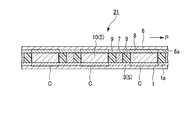
- FIG. 2 is a diagram of an electrical module manufactured by the electrical module manufacturing apparatus according to the present invention, and is a cross-sectional view taken along line X1-X1 in FIG.
- FIG. 3 is a diagram of a part (bonded substrate) of the configuration of the electric module shown in FIGS. 1 and 2, and is a cross-sectional view corresponding to a case taken along line X 1 -X 1 in FIG. 1.
- FIG. 1 is a plan view of an electrical module 21 that can be manufactured using the manufacturing apparatus 50 of the present embodiment.
- FIG. 2 is a view showing the electric module 21, and is a cross-sectional view taken along line X1-X1 shown in FIG.
- the electric module 21 is a film type dye-sensitized solar cell.
- the electric module 21 includes a first electrode 5, a wiring 7, and a sealing ultraviolet curable resin (ultraviolet curable resin) in different regions of the plate surface (one plate surface) 1 a.
- the first substrate 1 is a member serving as a base for the first electrode 5, the partition wall 9 and the wiring 7.
- substrate 1 will not be specifically limited if it has the moderate softness
- transparent resin materials such as polyethylene terephthalate (PET), acrylic, polycarbonate, polyethylene naphthalate (PEN), and polyimide.
- a transparent conductive film 3 is formed on the plate surface 1a of the first substrate 1 by sputtering or printing.
- the transparent conductive film 3 for example, tin oxide (ITO), zinc oxide or the like is used.
- the semiconductor layer 10 constitutes the first electrode 5 of the electric module 21 together with the transparent conductive film 3.
- the semiconductor layer 10 is made of, for example, a metal oxide having a function of receiving and transporting electrons from a sensitizing dye. Examples of such metal oxides include titanium oxide (TiO 2 ), zinc oxide (ZnO), and tin oxide (SnO 2 ).
- the semiconductor layer 10 carries a sensitizing dye (not shown).
- the sensitizing dye is composed of an organic dye or a metal complex dye.
- the organic dye for example, various organic dyes such as coumarin, polyene, cyanine, hemicyanine, and thiophene can be used.
- a ruthenium complex is preferably used as the metal complex dye.
- wiring 7 is provided between the semiconductor layers 10 via the partition walls 9. It should be noted that only the partition walls 9 are provided between the semiconductor layers 10 at locations where the wiring 7 is not necessary as the wiring pattern of the electric module 21.
- the wiring 7 is, for example, a conductive material such as copper or a paste containing the conductive material.
- the sealing ultraviolet curable resin forming the partition wall 9 is a resin that is cured by irradiation with ultraviolet rays.
- the wavelength of the ultraviolet light is, for example, 300 nm or more and 450 nm.
- the second substrate 6 is made of a transparent resin material or the like, like the first substrate 1.
- a second electrode 8 is formed on the plate surface 6a of the second substrate 6 by sputtering or printing.
- ITO ITO, platinum, polyaniline, polyethylenedioxythiophene (PEDOT), carbon, or the like is used for the second electrode 8.
- the gap when a gap is generated between the semiconductor layer 10 and the second electrode 8, the gap may be filled with an electrolytic solution.
- the electrolytic solution for example, a solution in which a supporting electrolyte such as lithium iodide and iodine are mixed in a liquid component such as ionic liquid such as acetonitrile, dimethylpropylimidazolium iodide, or butylmethylimidazolium iodide (propio And non-aqueous solvents such as nitrile).
- the cell C of the electric module 21 includes a semiconductor layer 10 and a first electrode 5 and a second electrode 8 arranged so as to face each other with the semiconductor layer 10 interposed therebetween.
- the electric module 21 includes the first substrate 1 in which the first electrode 5, the partition wall 9, and the wiring 7 are formed in different regions of the plate surface 1 a (surface facing the second substrate 6). (Hereinafter referred to as a bonded substrate 11) and a second substrate 6 (hereinafter referred to as a bonded substrate 12) in which the second electrode 8 is formed on the plate surface 6a, and bonded to each other from a separated state. Manufactured. In consideration of the ease of manufacture of the electric module 21, a notch may be formed in the plate surface 1 a of the first substrate 1 or the plate surface 6 a of the second substrate 6.
- the semiconductor layer 10, the partition wall 9, and the wiring 7 on the transparent conductive film 3 of the first substrate 1 are each expanded when pressed from above and below. Therefore, they may be provided with a gap corresponding to the size to be expanded.
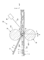
- FIG. 4 shows the configuration of the manufacturing apparatus 50 of the present embodiment, and is a view for explaining the manufacturing method of the electric module 21, which is a side (that is, orthogonal to the Z direction parallel to the vertical direction and is a base material) It is sectional drawing seen from the direction orthogonal to the P direction in which the is conveyed.
- the manufacturing apparatus 50 presses the bonded substrate 11 and the bonded substrate 12 from above and below so that the semiconductor layer 10 of the first electrode 5 and the second electrode 8 face each other.
- a pair of rollers 31 and 32 hereinafter referred to as a first roller 31 and a second roller 32
- the outside of the pressing region R where the first substrate 1 and the second substrate 6 are pressed by the pair of rollers 31 and 32 are pressed by the pair of rollers 31 and 32.
- an ultraviolet irradiation unit 36 that emits ultraviolet UV that cures the sealing ultraviolet curable resin that forms the partition wall 9.
- the pair of rollers 31 and 32 are arranged along the vertical direction with a predetermined interval in consideration of the thickness dimension of the electric module 21 shown in FIG.
- the electric module 21 may be an electric module 21B shown in FIG.
- FIG. 5 is a plan view illustrating the configuration of the manufacturing apparatus 50 of the present embodiment and illustrating the method for manufacturing the electric module 21.
- an ultraviolet reflecting portion 38 is provided on at least a part of the outer peripheral surfaces 31 ⁇ / b> S and 32 ⁇ / b> S of the pair of rollers 31 and 32.
- the ultraviolet reflecting part 38 is made of a material that reflects the ultraviolet UV emitted from the ultraviolet irradiating part 36. Further, the ultraviolet reflecting portion 38 is for reflecting the ultraviolet UV toward at least the pressing region R in which the sealing ultraviolet curable resin forming the partition wall 9 is sandwiched.
- the pair of rollers 31 and 32 are arranged along the vertical direction with an interval substantially equal to the thickness dimension of the electric module 21 shown in FIG.
- the ultraviolet irradiation unit 36 is provided on the downstream side in the P direction where the bonded substrate 11 and the bonded substrate 12 are conveyed with respect to the pair of rollers 31 and 32.
- the ultraviolet irradiation unit 36 is configured by a commercially available ultraviolet light source or an ultraviolet UV emitting unit (head or the like) guided from the ultraviolet light source installed at a distant place by an optical fiber or the like.
- the power in the pressing region R of the ultraviolet UV emitted from the ultraviolet irradiation unit 36 is not particularly limited as long as it is larger than the power required for curing the ultraviolet curable resin for sealing the partition wall 9, for example.
- the ultraviolet ray UV emitted from the ultraviolet ray irradiation unit 36 hits the outer peripheral surface 32S of the second roller 32 disposed on the lower side, is reflected toward the outer peripheral surface 31S of the first roller 31, and is applied to the pressing region R. .
- the ultraviolet rays UV hit the outer peripheral surface 31S of the first roller 31 and are reflected toward the upstream side of the pressing region R.
- the ultraviolet ray UV is irradiated to the pressing region R by reciprocating while reflecting between the outer peripheral surfaces 31S and 32S of the pair of rollers 31 and 32.
- the ultraviolet reflectance is preferably 50% or more and the diffuse reflectance is preferably 50% or less.
- the ultraviolet irradiation part 36 is in the press area
- the ultraviolet rays UV can be reflected by the outer peripheral surfaces 31S and 32S of the rollers 31 and 32, they may be disposed at any position.
- the outer peripheral surfaces 31S and 32S of the pair of rollers 31 and 32 may be mirror-finished or the like in order to easily reflect the ultraviolet rays UV.
- the material constituting at least the outer peripheral surfaces 31S and 32S of the rollers 31 and 32 is not particularly limited as long as it is a material that reflects ultraviolet rays UV.
- metal such as mirror-finished iron, aluminum, titanium, stainless steel (SUS), or the alloy containing the metal is mentioned, for example.
- the outer peripheral surfaces 31S and 32S of the rollers 31 and 32 may be plated.
- the ultraviolet rays UV are easily reflected. Since at least the ultraviolet reflecting portion 38 of the pair of rollers 31 and 32 is made of iron or stainless steel, the ultraviolet reflectance is improved to 50% or more with respect to the ultraviolet UV having a wavelength of 300 nm to 450 nm, and the diffuse reflectance is increased. 50% or less.
- the ultraviolet reflecting part 38 is located at least on the outer peripheral surfaces 31S and 32S of the rollers 31 and 32 facing the partition wall 9. As shown in FIG. 5, in this embodiment, of the outer peripheral surfaces 31S and 32S of the rollers 31 and 32, the portion facing the partition wall 9, that is, the central portion in the width direction of the rollers 31 and 32 is made of stainless steel, and the ultraviolet rays The reflection portion 38 is formed. Moreover, the ultraviolet reflection part 38 does not need to be provided over the whole circumferential direction of the outer peripheral surfaces 31S and 32S of the rollers 31 and 32, and the bonded substrate 11 and the bonded substrate 12 are in the P direction (that is, the transport direction).
- the partition 9 may be provided in the part which intermittently opposes when it moves.
- the whole rollers 31 and 32 may be comprised from the material which reflects ultraviolet-ray UV as mentioned above.
- the bonded substrate 11 and the second electrode 8 are arranged so that the semiconductor layer 10 of the first electrode 5 and the second electrode 8 face each other. Then, the bonded substrate 12 is brought close to the pair of rollers 31 and 32.
- the bonded substrate 11 and the bonded substrate 12 that are brought close to each other as described above are sandwiched and pressed by the pair of rollers 31 and 32 from above and below.
- the pressing region R is a bonded substrate from the position where the lower end of the first roller 31 disposed on the upper side and the upper end of the second roller 32 disposed on the lower side are closest.
- 11 and the bonded substrate 12 are in a range from the pressing force of the rollers 31 and 32 to the position where the components start to be restored.
- the bonded substrate 11 and the bonded substrate 12 are sandwiched by the rollers 31 and 32, and at the same time, the ultraviolet ray UV is emitted from the ultraviolet irradiation unit 36 and reflected by the ultraviolet reflection unit 38 on the downstream side of the pressing region R. .
- the ultraviolet ray UV is irradiated to the sealing ultraviolet curable resin of the partition wall 9 pressed from above and below by the rollers 31 and 32 in the pressing region R, and the sealing ultraviolet curable resin is cured.
- the electric module 21 manufactured as described above is supplied to the downstream side of the ultraviolet irradiation unit 36. Thereafter, in accordance with the wiring pattern or the like, the cell C is cut out, the wirings 7 are connected to each other, and the product of the electric module 21 is completed.
- the ultraviolet UV emitted from the ultraviolet irradiation unit 36 can be reflected toward the pressing region R by the ultraviolet reflecting unit 38.
- the ultraviolet curable resin for sealing that forms the partition wall 9 is vertically sandwiched between the pair of rollers 31 and 32, so that the bonded substrate 11 and the bonded substrate are pressed by the pair of rollers 31 and 32.
- the ultraviolet curable resin for sealing is cured and bonded without causing a gap between the substrates, and the wiring 7 is connected to the transparent conductive film 3 and the first substrate 1 of the first substrate 1. It can adhere well to the second electrode 8 of the two substrates 6 to form an electrical contact. Therefore, it is possible to prevent the occurrence of poor electrical connection in the wiring 7.
- the ultraviolet light reflection unit 38 is provided on the outer peripheral surfaces 31 ⁇ / b> S and 32 ⁇ / b> S of the rollers 31 and 32 facing the ultraviolet curable resin for sealing the partition wall 9. It is possible to efficiently reflect the pressure region R located in the vicinity of the reflecting portion 38.
- the material constituting the ultraviolet reflecting part 38 is made of iron or stainless steel, and the ultraviolet reflecting part 38 has an ultraviolet reflectance of 50% or more and a diffuse reflectance of 50% or less.
- the ultraviolet reflecting part 38 can be easily and relatively inexpensively configured using a material that can be easily processed into an arbitrary shape. Then, the UV UV emitted from the UV irradiation unit 36 can be reflected more efficiently to the pressing region R where the UV curable resin for sealing the partition wall 9 is sandwiched.
- the ultraviolet curable resin for sealing the partition wall 9 may be cured through two or more stages along the P direction.
- the ultraviolet irradiation unit 36 is provided as the first stage, and the ultraviolet irradiation unit other than the ultraviolet irradiation unit 36 is provided downstream of the ultraviolet irradiation unit 36 in the P direction from the second stage.
- the sealing UV curable resin is cured through the two steps as described above, first, as a first step, the UV irradiating unit 36 irradiates the UV reflecting unit 38 with UV UV, and then the bonded substrate.
- the sealing ultraviolet curable resin may be temporarily cured to the extent that the constituent elements 11 and 12 are released from the pressing force of the rollers 31 and 32 and are not restored.
- the ultraviolet curable resin for sealing the partition walls 9 of the bonded substrates 11 and 12 that are primarily bonded is applied to an ultraviolet ray different from the ultraviolet irradiation unit 36 on the downstream side of the pressing region R.
- the ultraviolet curable resin for sealing may be completely cured by irradiating ultraviolet rays from the irradiation unit.
- the pair of rollers 31 and 32 do not have to be circular when viewed from the side, and in order to ensure the length w of the pressing region R in the P direction, an elliptical core having a predetermined length w It may be a conveyor belt that moves along the outer peripheral surface of the material and is provided with an ultraviolet reflecting portion 38 on the outer peripheral surface.
- the film-type dye-sensitized solar cell was illustrated and demonstrated as the electrical module 21 which can be continuously produced in this embodiment, the electrical module 21 sandwiches the ultraviolet curable resin while transporting in the P direction. If it is an electric module which can be manufactured by bonding together, it will not be specifically limited. That is, the type of electric module and the shape and arrangement of each component are not particularly limited.
- the present invention can be used in the field related to electric modules such as solar cells.
Landscapes
- Engineering & Computer Science (AREA)
- Power Engineering (AREA)
- Microelectronics & Electronic Packaging (AREA)
- Hybrid Cells (AREA)
- Photovoltaic Devices (AREA)
- Electroluminescent Light Sources (AREA)
Abstract
本発明を適用した製造装置(50)は、少なくとも一方の表面上の互いに異なる領域に、第一電極(5)、紫外線硬化型樹脂により形成された封止用隔壁(隔壁)(9)及び配線(7)を有する第一基板(1)と、少なくとも一方の表面上に第二電極(8)を有する第二基板(6)と、を第一電極5及び第二電極(8)が対向するように、上下方向から挟んだ状態で押圧する一対のローラー(31,32)と、ローラー(31,32)によって第一基板(1)及び第二基板(6)が押圧されている押圧領域(R)の外方から紫外線硬化型樹脂を硬化させる紫外線(UV)を発する紫外線照射部(36)と、を備えている。ローラー(31,32)の外周面(31S,32S)のうち少なくとも一部には、紫外線(UV)を反射する材質からなると共に、紫外線(UV)を少なくとも封止用隔壁(9)が挟まれている押圧領域(R)に向けて反射する紫外線反射部(38)が設けられている。
Description
本発明は、電気モジュールの製造装置に関する。本願は、2015年9月17日に日本に出願された特願2015-184261号に基づき優先権を主張し、その内容をここに援用する。
近年、クリーンな発電源として、太陽電池が注目されている。太陽電池は、光エネルギーを直接かつ即時に電力に変換することができ、二酸化炭素等の汚染物質を排出しない発電源である。太陽電池の中でも、色素増感太陽電池は、高い変換効率を有し、比較的簡易な方法により製造され、且つ原材料単価が安価であるという優れた特徴を有し、次世代太陽電池として期待されている。
最近では、色素増感太陽電池をはじめとする太陽電池の実用化に向けて、ロール・ツー・ロール方式を導入した色素増感太陽電池の連続生産が導入されている。例えば、特許文献1には、酸化物半導体電極の製造方法が開示されている。この酸化物半導体電極の製造方法では、シート状の耐熱基板を長手方向にロールで搬送しながら、前記耐熱基板の板面に多孔質層形成用層を形成し、該多孔質層形成用層を焼成して多孔質層とした後、加熱された前記多孔質層に金属化合物を含む塗工液(電解液)を連続的に付与することにより前記多孔質層上に電極層を形成し、前記電極層上に樹脂材料からなる接着層と基材とを順次、連続的に貼り合わせ、前記耐熱基板を連続的に剥離する。
例えば、ロール・ツー・ロール方式を用いた色素増感太陽電池の連続生産では、多くの場合、電極及び配線が形成された二枚のフィルム状基板(以下、単に基板という場合もある)を厚み方向に間隔をあけて対向させ、基板同士を貼り合わせる。その後、貼り合わせてできたシート状の色素増感太陽電池から所定数のセルを切り出し、配線のパターンに合わせて適宜、直列又は並列に接続する。前述のように二枚の基板を貼り合わせて色素増感太陽電池とする際には、封止剤によって半導体層や配線を封止する必要がある。封止剤としては種々の材料が挙げられるが、紫外線硬化型樹脂が多用されている。
太陽電池等の電気モジュールの連続生産を行う際に、ロール・ツー・ロール方式を用いて二枚の基板を貼り合わせる工程では、所定のように対向配置されたフィルム状基板同士をゴムローラーで押圧することで、互いに密着させる。そして、密着状態のフィルム状基板間に設けられた紫外線硬化型樹脂に対し、ゴムローラーの下流側の位置で紫外線を照射することで、基板同士を接着すると共に、電気的接点を形成することができる。
しかしながら、ゴムローラーでは配線部分を長い間押圧することは難しく、ゴムローラーから排出された瞬間に、フィルム状基板同士を押圧する力が瞬時に開放されることで、フィルム状基板間の隙間が生じ易い。フィルム状基板間の隙間が生じることにより、フィルム状基板同士の配置が多少なりとも押圧前の状態に復元されてしまう。そして、ゴムローラーの設置されている位置から下流側の位置で紫外線を照射すると、ゴムローラーによって紫外線が遮られる、または吸収される場合がある。その場合、対向配置されたゴムローラー同士が最も近接し、かつフィルム状基板同士が押圧されている領域(押圧領域)に紫外線が照射されず、押圧領域よりも下流側で上述のようにフィルム状基板間の隙間が生じ易い位置に紫外線が照射されてしまう可能性がある。その結果、色素増感太陽電池の配線における電気的接続不良が引き起こされるという問題があった。
しかしながら、ゴムローラーでは配線部分を長い間押圧することは難しく、ゴムローラーから排出された瞬間に、フィルム状基板同士を押圧する力が瞬時に開放されることで、フィルム状基板間の隙間が生じ易い。フィルム状基板間の隙間が生じることにより、フィルム状基板同士の配置が多少なりとも押圧前の状態に復元されてしまう。そして、ゴムローラーの設置されている位置から下流側の位置で紫外線を照射すると、ゴムローラーによって紫外線が遮られる、または吸収される場合がある。その場合、対向配置されたゴムローラー同士が最も近接し、かつフィルム状基板同士が押圧されている領域(押圧領域)に紫外線が照射されず、押圧領域よりも下流側で上述のようにフィルム状基板間の隙間が生じ易い位置に紫外線が照射されてしまう可能性がある。その結果、色素増感太陽電池の配線における電気的接続不良が引き起こされるという問題があった。
本発明は、上述の問題を鑑みてなされたものであり、配線における電気的接続不良の発生を防止することができる電気モジュールの製造装置を提供する。
本発明の電気モジュールの製造装置は、一方の板面の互いに異なる領域に第一電極、紫外線硬化型樹脂及び配線が形成された第一基板と、一方の板面に第二電極が形成された第二基板と、を前記第一電極及び前記第二電極が対向するように、上下方向から挟んだ状態で押圧する一対のローラーと、前記一対のローラーによって前記第一基板及び前記第二基板が押圧されている押圧領域の外方から前記紫外線硬化型樹脂を硬化させる紫外線を発する紫外線照射部と、を備え、前記一対のローラーの外周面のうち少なくとも一部には、前記紫外線照射部から発せられた前記紫外線を反射する材質からなると共に、前記紫外線を少なくとも前記紫外線硬化型樹脂が挟まれている前記押圧領域に向けて反射する紫外線反射部が設けられていることを特徴とする。
上述の電気モジュールの製造装置によれば、紫外線照射部から発せられた紫外線が紫外線反射部によって紫外線硬化型樹脂が一対のローラーで挟まれている押圧領域に向けて反射される。従って、一対のローラーの押圧によって第一基板及び第二基板の密着状態が保持されている間に、紫外線硬化型樹脂が硬化し、基板間に隙間が生じることなく基板同士が接着すると共に、配線が第一基板及び第二基板に対して良好に接着され、電気的接点が形成されるので、配線における電気的接続不良の発生がなくなる。
上述の電気モジュールの製造装置によれば、紫外線照射部から発せられた紫外線が紫外線反射部によって紫外線硬化型樹脂が一対のローラーで挟まれている押圧領域に向けて反射される。従って、一対のローラーの押圧によって第一基板及び第二基板の密着状態が保持されている間に、紫外線硬化型樹脂が硬化し、基板間に隙間が生じることなく基板同士が接着すると共に、配線が第一基板及び第二基板に対して良好に接着され、電気的接点が形成されるので、配線における電気的接続不良の発生がなくなる。
本発明の電気モジュールの製造装置では、前記紫外線反射部は前記紫外線硬化型樹脂に対向する前記ローラーの外周面に位置していてもよい。
上述の電気モジュールの製造装置によれば、紫外線照射部から発せられた紫外線が紫外線反射部によって、紫外線反射部の近傍に位置する押圧領域に対して効率よく反射する。
上述の電気モジュールの製造装置によれば、紫外線照射部から発せられた紫外線が紫外線反射部によって、紫外線反射部の近傍に位置する押圧領域に対して効率よく反射する。
本発明の電気モジュールの製造装置では、前記紫外線を反射する材質として、例えば、鉄、アルミニウム、チタン又はステンレス等の金属又はその金属を含む合金等が挙げられる。前記紫外線反射部において、紫外線反射率は50%以上であり、拡散反射度は50%以下であることが好ましい。なお、前記材質は、紫外線を反射可能な材質であれば特に限定されない。また、前述の金属の表面に、クロムメッキ等のメッキ処理がなされてもよい。
なお、紫外線の波長は、例えば250nm以上450nm以下とすることができるが、紫外線硬化型樹脂を硬化可能な波長であれば特に限定されない。また、「紫外線反射率は50%以上である」及び「拡散反射度は50%以下である」とは、紫外線硬化型樹脂が硬化するのに最適な波長の紫外線の紫外線反射率が50%以上であり、前記最適な波長の拡散反射度が50%以上であることを示す。
上述の電気モジュールの製造装置によれば、入手容易で、且つ任意の形状に加工し易い材質である鉄又はステンレスによって紫外線反射部が構成される。そして、紫外線照射部から発せられた紫外線は、より高効率に、紫外線硬化型樹脂が挟まれている押圧領域に対して反射することができる。
なお、紫外線の波長は、例えば250nm以上450nm以下とすることができるが、紫外線硬化型樹脂を硬化可能な波長であれば特に限定されない。また、「紫外線反射率は50%以上である」及び「拡散反射度は50%以下である」とは、紫外線硬化型樹脂が硬化するのに最適な波長の紫外線の紫外線反射率が50%以上であり、前記最適な波長の拡散反射度が50%以上であることを示す。
上述の電気モジュールの製造装置によれば、入手容易で、且つ任意の形状に加工し易い材質である鉄又はステンレスによって紫外線反射部が構成される。そして、紫外線照射部から発せられた紫外線は、より高効率に、紫外線硬化型樹脂が挟まれている押圧領域に対して反射することができる。
本発明の電気モジュールの製造装置によれば、配線における電気的接続不良の発生を防止することができる。
以下、本発明を適用した一実施形態である電気モジュールの製造装置について、図面を参照して説明する。なお、以下の説明で用いる図面は模式的なものであり、長さ、幅、及び厚みの比率等は実際のものと同一とは限らず、適宜変更することができる。また、以下の説明において例示される材料等は一例であって、本発明はそれらに限定されるものではなく、本発明の要旨を変更しない範囲で適宜変更して実施することができる。
図1は、本実施形態の製造装置50を用いて製造可能な電気モジュール21の平面図である。図2は、電気モジュール21を示す図であり、図1に示すX1-X1線で矢視した断面図である。
電気モジュール21は、フィルム型の色素増感太陽電池である。図1及び図2に示すように、電気モジュール21は、板面(一方の板面)1aの互いに異なる領域に第一電極5、配線7と封止用紫外線硬化型樹脂(紫外線硬化型樹脂)により形成された隔壁9が形成された第一基板1と、板面(一方の板面)6aに第二電極8が形成された第二基板6と、を備えている。
電気モジュール21は、フィルム型の色素増感太陽電池である。図1及び図2に示すように、電気モジュール21は、板面(一方の板面)1aの互いに異なる領域に第一電極5、配線7と封止用紫外線硬化型樹脂(紫外線硬化型樹脂)により形成された隔壁9が形成された第一基板1と、板面(一方の板面)6aに第二電極8が形成された第二基板6と、を備えている。
第一基板1は、第一電極5、隔壁9及び配線7の基台となる部材である。第一基板1は、ロール・ツー・ロール方式等での太陽電池の連続生産に適用できる適度な柔軟性を有し、大面積フィルム状に形成可能な材質であれば特に限定されない。このような材質としては、例えば、ポリエチレンテレフタレート(PET)、アクリル、ポリカーボネート、ポリエチレンナフタレート(PEN)、ポリイミド等の透明の樹脂材料が挙げられる。
第一基板1の板面1aには、スパッタリング法や印刷法により、透明導電膜3が成膜されている。透明導電膜3には、例えば、酸化スズ(ITO)、酸化亜鉛等が用いられる。
透明導電膜3の上面には、互いに異なる領域に間隔をあけて複数の半導体層10が積層されている。半導体層10は、透明導電膜3とともに電気モジュール21の第一電極5を構成するものである。半導体層10は、例えば、増感色素から電子を受け取り輸送する機能を有する金属酸化物からなる。このような金属酸化物としては、例えば、酸化チタン(TiO2)、酸化亜鉛(ZnO)、酸化スズ(SnO2)、等が挙げられる。
半導体層10には、不図示の増感色素が担持されている。増感色素は、有機色素または金属錯体色素で構成されている。有機色素として、例えば、クマリン系、ポリエン系、シアニン系、ヘミシアニン系、チオフェン系、等の各種有機色素を用いることができる。金属錯体色素としては、例えば、ルテニウム錯体等、が好適に用いられる。
透明導電膜3の上には、半導体層10同士の間に、隔壁9を介して配線7が設けられている。なお、電気モジュール21の配線パターンとして配線7が不要な箇所では、半導体層10同士の間には隔壁9のみが設けられている。
配線7は、例えば銅等の導電材、或いは前記導電材を含むペーストである。
隔壁9を形成する封止用紫外線硬化型樹脂は、紫外線の照射により硬化する樹脂である。紫外線の波長は、例えば300nm以上450nmである。
配線7は、例えば銅等の導電材、或いは前記導電材を含むペーストである。
隔壁9を形成する封止用紫外線硬化型樹脂は、紫外線の照射により硬化する樹脂である。紫外線の波長は、例えば300nm以上450nmである。
第二基板6は、第一基板1と同様に透明の樹脂材料等から構成されている。
第二基板6の板面6aには、スパッタリング法や印刷法により、第二電極8が成膜されている。第二電極8には、例えば、ITO、プラチナ、ポリアニリン、ポリエチレンジオキシチオフェン(PEDOT)、カーボン等が用いられる。
第二基板6の板面6aには、スパッタリング法や印刷法により、第二電極8が成膜されている。第二電極8には、例えば、ITO、プラチナ、ポリアニリン、ポリエチレンジオキシチオフェン(PEDOT)、カーボン等が用いられる。
なお、半導体層10と第二電極8との間に隙間が生じている際には、その隙間に電解液が充填されていてもよい。電解液としては、例えば、アセトニトリル、ヨウ化ジメチルプロピルイミダゾリウムまたはヨウ化ブチルメチルイミダゾリウム等のイオン液体などの液体成分に、ヨウ化リチウム等の支持電解質とヨウ素とが混合された溶液(プロピオニトリル等の非水系溶剤)等の液体が挙げられる。
電気モジュール21のセルCは、半導体層10と、半導体層10を挟んで互いに対向するように配置された第一電極5と第二電極8から構成されている。
図3に示すように、電気モジュール21は、板面1a(第二基板6に対向している面)の互いに異なる領域に第一電極5、隔壁9及び配線7が形成された第一基板1(以下、貼り合わせ基板11とする)と、板面6aに第二電極8が形成された第二基板6(以下、貼り合わせ基板12とする)と、それぞれを分離した状態から互いに貼り合わせて製造される。
なお、電気モジュール21の製造容易性等を考慮し、第一基板1の板面1a、或いは第二基板6の板面6aに、切り欠きが形成されていてもよい。また、第二基板6との貼り合わせ前において、第一基板1の透明導電膜3上の半導体層10、隔壁9及び配線7は、上下方向から押圧された際にそれぞれ押し拡げられ、その状態で固定されることから、互いに、押し拡げられる寸法分の隙間をあけて設けられていてもよい。
なお、電気モジュール21の製造容易性等を考慮し、第一基板1の板面1a、或いは第二基板6の板面6aに、切り欠きが形成されていてもよい。また、第二基板6との貼り合わせ前において、第一基板1の透明導電膜3上の半導体層10、隔壁9及び配線7は、上下方向から押圧された際にそれぞれ押し拡げられ、その状態で固定されることから、互いに、押し拡げられる寸法分の隙間をあけて設けられていてもよい。
図4は、本実施形態の製造装置50の構成を示し、電気モジュール21の製造方法を説明するための図であり、側方(即ち、鉛直方向に平行なZ方向に直交し、且つ基材が搬送されるP方向に直交する方向)から見た断面図である。
図4に示すように、製造装置50は、第一電極5の半導体層10と第二電極8が対向するように、貼り合わせ基板11と貼り合わせ基板12とを上下方向から挟んだ状態で押圧する一対のローラー31,32(以下、第一ローラー31、第二ローラー32とする)と、一対のローラー31,32によって第一基板1及び第二基板6が押圧されている押圧領域Rの外方から隔壁9を形成する封止用紫外線硬化型樹脂を硬化させる紫外線UVを発する紫外線照射部36と、を備えている。
一対のローラー31,32は、図2に示す電気モジュール21の厚み寸法を勘案した所定の間隔をあけて上下方向に沿って配置されている。
なお、電気モジュール21は、図6に示す電気モジュール21Bであってもよい。
図4に示すように、製造装置50は、第一電極5の半導体層10と第二電極8が対向するように、貼り合わせ基板11と貼り合わせ基板12とを上下方向から挟んだ状態で押圧する一対のローラー31,32(以下、第一ローラー31、第二ローラー32とする)と、一対のローラー31,32によって第一基板1及び第二基板6が押圧されている押圧領域Rの外方から隔壁9を形成する封止用紫外線硬化型樹脂を硬化させる紫外線UVを発する紫外線照射部36と、を備えている。
一対のローラー31,32は、図2に示す電気モジュール21の厚み寸法を勘案した所定の間隔をあけて上下方向に沿って配置されている。
なお、電気モジュール21は、図6に示す電気モジュール21Bであってもよい。
図5は、本実施形態の製造装置50の構成を示し、電気モジュール21の製造方法を説明するための平面図である。
図4及び図5に示すように、一対のローラー31,32の外周面31S,32Sのうち少なくとも一部には、紫外線反射部38が設けられている。紫外線反射部38は、紫外線照射部36から発せられた紫外線UVを反射する材質からなる。また、紫外線反射部38は、紫外線UVを少なくとも隔壁9を形成する封止用紫外線硬化型樹脂が挟まれている押圧領域Rに向けて反射するためのものである。
一対のローラー31,32は、互いに図2に示す電気モジュール21の厚み寸法と略同等の間隔をあけて上下方向に沿って配置されている。
図4及び図5に示すように、一対のローラー31,32の外周面31S,32Sのうち少なくとも一部には、紫外線反射部38が設けられている。紫外線反射部38は、紫外線照射部36から発せられた紫外線UVを反射する材質からなる。また、紫外線反射部38は、紫外線UVを少なくとも隔壁9を形成する封止用紫外線硬化型樹脂が挟まれている押圧領域Rに向けて反射するためのものである。
一対のローラー31,32は、互いに図2に示す電気モジュール21の厚み寸法と略同等の間隔をあけて上下方向に沿って配置されている。
紫外線照射部36は、一対のローラー31,32に対して、貼り合わせ基板11及び貼り合わせ基板12が搬送されるP方向の下流側上方に設けられている。
紫外線照射部36は、市販の紫外線光源、又は、離れた場所に設置された前記紫外線光源から光ファイバ等で導かれた紫外線UVの出射部(ヘッド等)で構成されている。紫外線照射部36から出射される紫外線UVの押圧領域Rにおけるパワーは、例えば隔壁9の封止用紫外線硬化型樹脂の硬化に必要なパワーより大きければよく、特に限定されない。
紫外線照射部36は、市販の紫外線光源、又は、離れた場所に設置された前記紫外線光源から光ファイバ等で導かれた紫外線UVの出射部(ヘッド等)で構成されている。紫外線照射部36から出射される紫外線UVの押圧領域Rにおけるパワーは、例えば隔壁9の封止用紫外線硬化型樹脂の硬化に必要なパワーより大きければよく、特に限定されない。
紫外線照射部36から発せられた紫外線UVは、下側に配置されている第二ローラー32の外周面32Sに当たり、第一ローラー31の外周面31Sに向かって反射して押圧領域Rに照射される。紫外線UVは、第一ローラー31の外周面31Sに当たり、押圧領域Rの上流側に向かって反射する。前述のように、紫外線UVが一対のローラー31,32の外周面31S,32S間を反射しながら往復することで、押圧領域Rに照射される。
このとき、紫外線UVを反射する条件として、紫外線反射率は50%以上であって、拡散反射度は50%以下であることが好ましい。
なお、紫外線照射部36は、第一基板1及び第二基板6によって隔壁9の封止用紫外線硬化型樹脂が挟まれている(即ち、封止用紫外線硬化型樹脂を含む)押圧領域Rに向かって、紫外線UVをローラー31,32の外周面31S,32Sで反射させることができれば、何れの位置に配されていても構わない。
このとき、紫外線UVを反射する条件として、紫外線反射率は50%以上であって、拡散反射度は50%以下であることが好ましい。
なお、紫外線照射部36は、第一基板1及び第二基板6によって隔壁9の封止用紫外線硬化型樹脂が挟まれている(即ち、封止用紫外線硬化型樹脂を含む)押圧領域Rに向かって、紫外線UVをローラー31,32の外周面31S,32Sで反射させることができれば、何れの位置に配されていても構わない。
一対のローラー31,32の外周面31S,32Sは、紫外線UVを反射しやすくするために、鏡面加工等がなされていてもよい。ローラー31,32の少なくとも外周面31S,32Sを構成する材質は、紫外線UVを反射する材質であれば特に限定されない。ローラー31,32の外周面31S,32Sを構成する材質としては、例えば鏡面加工された鉄、アルミニウム、チタン又はステンレス(SUS)等の金属又はその金属を含む合金が挙げられる。強度や耐久性を高めるために、ローラー31,32の外周面31S,32Sに、メッキ処理が行われていてもよい。ローラー31,32の外周面31S,32Sにメッキ処理が施されることで紫外線UVが反射しやすくなる。
一対のローラー31,32の少なくとも紫外線反射部38が鉄又はステンレスで構成されていることにより、波長300nmから450nmの紫外線UVに対して、紫外線反射率が50%以上に向上し、拡散反射度が50%以下に抑えられる。
一対のローラー31,32の少なくとも紫外線反射部38が鉄又はステンレスで構成されていることにより、波長300nmから450nmの紫外線UVに対して、紫外線反射率が50%以上に向上し、拡散反射度が50%以下に抑えられる。
紫外線反射部38は、少なくとも隔壁9に対向するローラー31,32の外周面31S,32Sに位置している。図5に示すように、本実施形態では、ローラー31,32の外周面31S,32Sのうち、隔壁9に対向する部分、即ちローラー31,32の幅方向の中央部分がステンレスから構成され、紫外線反射部38となっている。
また、紫外線反射部38は、ローラー31,32の外周面31S,32Sの周方向全体にわたって設けられていなくてもよく、貼り合わせ基板11及び貼り合わせ基板12がP方向(即ち、搬送方向)に移動したときに、隔壁9が断続的に対向する部分に設けられていてもよい。
なお、ローラー31,32の全体が上述したように紫外線UVを反射する材質から構成されていてもよい。
また、紫外線反射部38は、ローラー31,32の外周面31S,32Sの周方向全体にわたって設けられていなくてもよく、貼り合わせ基板11及び貼り合わせ基板12がP方向(即ち、搬送方向)に移動したときに、隔壁9が断続的に対向する部分に設けられていてもよい。
なお、ローラー31,32の全体が上述したように紫外線UVを反射する材質から構成されていてもよい。
図4に示すように、上述の製造装置50を用いて電気モジュール21を製造する際には、第一電極5の半導体層10と第二電極8とが対向するように、貼り合わせ基板11と、貼り合わせ基板12とを一対のローラー31,32に向かって近接させる。
次に、上述のように互いに近接させた貼り合わせ基板11及び貼り合わせ基板12を、一対のローラー31,32によって上下方向から挟むと共に押圧する。基材が搬送されるP方向において、押圧領域Rは、上側に配置された第一ローラー31の下端と下側に配置された第二ローラー32の上端とが最も接近した位置から、貼り合わせ基板11及び貼り合わせ基板12のそれぞれの構成要素がローラー31,32による押圧力から開放されて復元し始める位置までの範囲である。前述のようにローラー31,32によって貼り合わせ基板11及び貼り合わせ基板12を挟むと同時に、押圧領域Rの下流側において、紫外線照射部36から紫外線UVを出射すると共に、紫外線反射部38によって反射させる。これにより、押圧領域Rにおいてローラー31,32により上下方向から押圧された状態の隔壁9の封止用紫外線硬化型樹脂に対して紫外線UVが照射され、封止用紫外線硬化型樹脂が硬化する。紫外線照射部36の下流側には、上述のように製造された電気モジュール21が供給される。
この後、配線パターン等に合わせて、セルCの切り出しや配線7同士の接続等を行い、電気モジュール21の製品が完成する。
この後、配線パターン等に合わせて、セルCの切り出しや配線7同士の接続等を行い、電気モジュール21の製品が完成する。
以上説明した本実施形態の製造装置50によれば、紫外線照射部36から発せられた紫外線UVを紫外線反射部38によって押圧領域Rに向けて反射することができる。押圧領域Rでは隔壁9を形成する封止用紫外線硬化型樹脂が一対のローラー31,32によって上下方向に挟まれているので、一対のローラー31,32の押圧によって貼り合わせ基板11及び貼り合わせ基板12の密着状態が保持されている間に、封止用紫外線硬化型樹脂を硬化させ、基板間に隙間を生じさせることなく接着すると共に、配線7を第一基板1の透明導電膜3及び第二基板6の第二電極8に対して良好に接着し、電気的接点を形成することができる。従って、配線7における電気的接続不良の発生を防止することができる。
また、製造装置50において、紫外線反射部38を隔壁9の封止用紫外線硬化型樹脂に対向するローラー31,32の外周面31S,32Sに設けることで、紫外線反射部38によって、紫外線UVを紫外線反射部38の近傍に位置する押圧領域Rに対して効率よく反射させることができる。
また、製造装置50において、紫外線反射部38を構成する材質を鉄又はステンレスとし、紫外線反射部38において、紫外線反射率を50%以上、拡散反射度を50%以下とすることで、入手容易で、且つ任意の形状に加工し易い材質を用いて紫外線反射部38を容易に且つ比較的安価で構成することができる。そして、紫外線照射部36から発せられた紫外線UVを、隔壁9の封止用紫外線硬化型樹脂が挟まれている押圧領域Rに対して、より高効率に反射させることができる。
また、製造装置50において、紫外線反射部38を構成する材質を鉄又はステンレスとし、紫外線反射部38において、紫外線反射率を50%以上、拡散反射度を50%以下とすることで、入手容易で、且つ任意の形状に加工し易い材質を用いて紫外線反射部38を容易に且つ比較的安価で構成することができる。そして、紫外線照射部36から発せられた紫外線UVを、隔壁9の封止用紫外線硬化型樹脂が挟まれている押圧領域Rに対して、より高効率に反射させることができる。
以上、本発明の好ましい実施形態について詳述したが、本発明は係る特定の実施形態に限定されるものではなく、特許請求の範囲内に記載された本発明の要旨の範囲内において、種々の変形・変更が可能である。
例えば、P方向に沿って二段階以上の複数の段階を経て隔壁9の封止用紫外線硬化型樹脂を硬化させてもよい。即ち、一段階目として紫外線照射部36が設けられ、二段階目以降として、紫外線照射部36よりもP方向の下流側に、紫外線照射部36とは別の紫外線照射部が設けられていてもよい。前述のように二段階を経て封止用紫外線硬化型樹脂の硬化を行う場合は、先ず、一段階目として、紫外線照射部36から紫外線反射部38に対して紫外線UVを照射し、貼り合わせ基板11,12のそれぞれの構成要素がローラー31,32による押圧力から開放されて復元しない程度に封止用紫外線硬化型樹脂を一次的に硬化させてもよい。その後、二段階目として、一次的に貼り合された貼り合わせ基板11,12の隔壁9の封止用紫外線硬化型樹脂に、押圧領域Rよりも下流側において紫外線照射部36とは別の紫外線照射部から紫外線を照射することで、封止用紫外線硬化型樹脂を完全に硬化させてもよい。
また、一対のローラー31,32は側面視真円形でなくてもよく、P方向における押圧領域Rの長さ寸法wを確保するために、所定の長さ寸法wを有する側面視楕円形の芯材の外周面に沿って移動し、外周面に紫外線反射部38が設けられた搬送ベルトであってもよい。
また、本実施形態における連続生産可能な電気モジュール21としてフィルム型の色素増感太陽電池を例示して説明したが、電気モジュール21は、P方向に搬送しながら紫外線硬化型樹脂を挟んで基板同士を貼り合わせることで製造可能な電気モジュールであれば、特に限定されない。即ち、電気モジュールの種類や各構成要素の形状及び配置は、特に限定されない。
本発明は、太陽電池等の電気モジュールに関する分野で利用可能である。
1…第一基板
1a,6a…板面
5…第一電極
7…配線
8…第二電極
9…隔壁
21,21B…電気モジュール
31,32…ローラー
31S,32S…外周面
36…紫外線照射部
38…紫外線反射部
50…製造装置(電気モジュールの製造装置)
R…押圧領域
1a,6a…板面
5…第一電極
7…配線
8…第二電極
9…隔壁
21,21B…電気モジュール
31,32…ローラー
31S,32S…外周面
36…紫外線照射部
38…紫外線反射部
50…製造装置(電気モジュールの製造装置)
R…押圧領域
Claims (3)
- 一方の表面上の互いに異なる領域に、第一電極及び紫外線硬化型樹脂により形成された隔壁を有する第一基板と、一方の表面上に第二電極を有する第二基板と、を前記第一電極及び前記第二電極が対向するように、上下方向から挟んだ状態で押圧する一対のローラーと、
前記一対のローラーによって前記第一基板及び前記第二基板が押圧されている押圧領域の外方から前記紫外線硬化型樹脂を硬化させる紫外線を発する紫外線照射部と、
を備え、
前記一対のローラーの外周面のうち少なくとも一部には、前記紫外線照射部から発せられた前記紫外線を反射する材質からなると共に、前記紫外線を少なくとも前記隔壁が挟まれている前記押圧領域に向けて反射する紫外線反射部が設けられている電気モジュールの製造装置。 - 前記紫外線反射部は前記隔壁に対向する前記ローラーの外周面に位置している請求項1に記載の電気モジュールの製造装置。
- 前記紫外線を反射する材質は、鉄、アルミニウム、チタン及びステンレスからなる群より選ばれる金属又はその金属を含む合金であり、
前記紫外線反射部において、紫外線反射率は50%以上であり、拡散反射度は50%以下である請求項1又は請求項2に記載の電気モジュールの製造装置。
Applications Claiming Priority (2)
| Application Number | Priority Date | Filing Date | Title |
|---|---|---|---|
| JP2015184261A JP6530686B2 (ja) | 2015-09-17 | 2015-09-17 | 電気モジュールの製造装置 |
| JP2015-184261 | 2015-09-17 |
Publications (1)
| Publication Number | Publication Date |
|---|---|
| WO2017047690A1 true WO2017047690A1 (ja) | 2017-03-23 |
Family
ID=58289280
Family Applications (1)
| Application Number | Title | Priority Date | Filing Date |
|---|---|---|---|
| PCT/JP2016/077246 Ceased WO2017047690A1 (ja) | 2015-09-17 | 2016-09-15 | 電気モジュールの製造装置 |
Country Status (3)
| Country | Link |
|---|---|
| JP (1) | JP6530686B2 (ja) |
| TW (1) | TW201735388A (ja) |
| WO (1) | WO2017047690A1 (ja) |
Citations (4)
| Publication number | Priority date | Publication date | Assignee | Title |
|---|---|---|---|---|
| JP2007033545A (ja) * | 2005-07-22 | 2007-02-08 | Sony Chemical & Information Device Corp | 電気化学セルおよびその製造方法 |
| JP2014102977A (ja) * | 2012-11-20 | 2014-06-05 | Sekisui Chem Co Ltd | 電気モジュールの製造方法及び電気モジュール |
| WO2014112624A1 (ja) * | 2013-01-18 | 2014-07-24 | 積水化学工業株式会社 | 電気デバイス及び電気デバイスの製造方法 |
| WO2015008227A1 (en) * | 2013-07-15 | 2015-01-22 | 3Gsolar Photovoltaics Ltd. | Plastic solar dye cells |
-
2015
- 2015-09-17 JP JP2015184261A patent/JP6530686B2/ja active Active
-
2016
- 2016-09-14 TW TW105130102A patent/TW201735388A/zh unknown
- 2016-09-15 WO PCT/JP2016/077246 patent/WO2017047690A1/ja not_active Ceased
Patent Citations (4)
| Publication number | Priority date | Publication date | Assignee | Title |
|---|---|---|---|---|
| JP2007033545A (ja) * | 2005-07-22 | 2007-02-08 | Sony Chemical & Information Device Corp | 電気化学セルおよびその製造方法 |
| JP2014102977A (ja) * | 2012-11-20 | 2014-06-05 | Sekisui Chem Co Ltd | 電気モジュールの製造方法及び電気モジュール |
| WO2014112624A1 (ja) * | 2013-01-18 | 2014-07-24 | 積水化学工業株式会社 | 電気デバイス及び電気デバイスの製造方法 |
| WO2015008227A1 (en) * | 2013-07-15 | 2015-01-22 | 3Gsolar Photovoltaics Ltd. | Plastic solar dye cells |
Also Published As
| Publication number | Publication date |
|---|---|
| JP6530686B2 (ja) | 2019-06-12 |
| TW201735388A (zh) | 2017-10-01 |
| JP2018181862A (ja) | 2018-11-15 |
Similar Documents
| Publication | Publication Date | Title |
|---|---|---|
| EP3211674B1 (en) | Array substrate and preparation method thereof, flexible display panel and display device | |
| WO2016017776A1 (ja) | 太陽電池の製造方法 | |
| JP6501856B1 (ja) | 有機電子デバイスの製造方法 | |
| JP6286110B2 (ja) | 電気モジュールの製造方法および電気モジュールの製造装置 | |
| US20170117420A1 (en) | Method for fabricating solar panel module | |
| JP6530686B2 (ja) | 電気モジュールの製造装置 | |
| JP6918521B2 (ja) | 電気モジュールおよび電気モジュールの製造方法 | |
| TW201444106A (zh) | 電氣裝置及電氣裝置之製造方法 | |
| KR20160045621A (ko) | 광전 변환 소자 및 광전 변환 소자의 제조 방법 | |
| JP6043166B2 (ja) | 電気モジュールの製造方法及び電気モジュール | |
| JP2017059721A (ja) | 電気モジュールの製造装置 | |
| JP2020043199A (ja) | 色素増感型太陽電池 | |
| JP6687457B2 (ja) | 電気モジュール、色素増感太陽電池及び電気モジュールの製造方法 | |
| JP2013093411A (ja) | バックコンタクト回路付きバックシートの製造方法およびバックコンタクト回路付きバックシートおよびそれを用いた太陽電池モジュール | |
| JP6595894B2 (ja) | 粘性体供給装置、及び色素増感太陽電池の製造方法 | |
| CN110431648B (zh) | 层叠体和有机系太阳能电池的制造方法 | |
| US20140076393A1 (en) | Flexible solar cell and manufacturing method thereof | |
| JP7613437B2 (ja) | 全固体電池の製造方法 | |
| JP6412396B2 (ja) | 色素増感太陽電池の製造方法 | |
| WO2019146684A1 (ja) | 電気モジュール及び電気モジュールの製造方法 | |
| JP6666724B2 (ja) | 光電変換素子、この光電変換素子を設置した構造体及び光電変換素子の製造方法 | |
| JP6703574B2 (ja) | 電気モジュールおよびその製造方法 | |
| JP2019004059A (ja) | 電気モジュール及び電気モジュールの製造方法 | |
| JP2018041908A (ja) | 電気モジュールの製造方法及び電気モジュールの製造装置 | |
| JP2017073308A (ja) | 有機電子素子の製造方法、及び、有機電子素子 |
Legal Events
| Date | Code | Title | Description |
|---|---|---|---|
| 121 | Ep: the epo has been informed by wipo that ep was designated in this application |
Ref document number: 16846561 Country of ref document: EP Kind code of ref document: A1 |
|
| NENP | Non-entry into the national phase |
Ref country code: DE |
|
| 122 | Ep: pct application non-entry in european phase |
Ref document number: 16846561 Country of ref document: EP Kind code of ref document: A1 |
|
| NENP | Non-entry into the national phase |
Ref country code: JP |