WO2017046844A1 - レーザシステム - Google Patents
レーザシステム Download PDFInfo
- Publication number
- WO2017046844A1 WO2017046844A1 PCT/JP2015/076010 JP2015076010W WO2017046844A1 WO 2017046844 A1 WO2017046844 A1 WO 2017046844A1 JP 2015076010 W JP2015076010 W JP 2015076010W WO 2017046844 A1 WO2017046844 A1 WO 2017046844A1
- Authority
- WO
- WIPO (PCT)
- Prior art keywords
- charging
- laser
- voltage
- charging capacitor
- pulse
- Prior art date
- Legal status (The legal status is an assumption and is not a legal conclusion. Google has not performed a legal analysis and makes no representation as to the accuracy of the status listed.)
- Ceased
Links
Images








Classifications
-
- H—ELECTRICITY
- H01—ELECTRIC ELEMENTS
- H01S—DEVICES USING THE PROCESS OF LIGHT AMPLIFICATION BY STIMULATED EMISSION OF RADIATION [LASER] TO AMPLIFY OR GENERATE LIGHT; DEVICES USING STIMULATED EMISSION OF ELECTROMAGNETIC RADIATION IN WAVE RANGES OTHER THAN OPTICAL
- H01S3/00—Lasers, i.e. devices using stimulated emission of electromagnetic radiation in the infrared, visible or ultraviolet wave range
- H01S3/09—Processes or apparatus for excitation, e.g. pumping
- H01S3/097—Processes or apparatus for excitation, e.g. pumping by gas discharge of a gas laser
- H01S3/09702—Details of the driver electronics and electric discharge circuits
-
- H—ELECTRICITY
- H01—ELECTRIC ELEMENTS
- H01S—DEVICES USING THE PROCESS OF LIGHT AMPLIFICATION BY STIMULATED EMISSION OF RADIATION [LASER] TO AMPLIFY OR GENERATE LIGHT; DEVICES USING STIMULATED EMISSION OF ELECTROMAGNETIC RADIATION IN WAVE RANGES OTHER THAN OPTICAL
- H01S3/00—Lasers, i.e. devices using stimulated emission of electromagnetic radiation in the infrared, visible or ultraviolet wave range
- H01S3/10—Controlling the intensity, frequency, phase, polarisation or direction of the emitted radiation, e.g. switching, gating, modulating or demodulating
- H01S3/102—Controlling the intensity, frequency, phase, polarisation or direction of the emitted radiation, e.g. switching, gating, modulating or demodulating by controlling the active medium, e.g. by controlling the processes or apparatus for excitation
- H01S3/104—Controlling the intensity, frequency, phase, polarisation or direction of the emitted radiation, e.g. switching, gating, modulating or demodulating by controlling the active medium, e.g. by controlling the processes or apparatus for excitation in gas lasers
-
- H—ELECTRICITY
- H01—ELECTRIC ELEMENTS
- H01S—DEVICES USING THE PROCESS OF LIGHT AMPLIFICATION BY STIMULATED EMISSION OF RADIATION [LASER] TO AMPLIFY OR GENERATE LIGHT; DEVICES USING STIMULATED EMISSION OF ELECTROMAGNETIC RADIATION IN WAVE RANGES OTHER THAN OPTICAL
- H01S3/00—Lasers, i.e. devices using stimulated emission of electromagnetic radiation in the infrared, visible or ultraviolet wave range
- H01S3/14—Lasers, i.e. devices using stimulated emission of electromagnetic radiation in the infrared, visible or ultraviolet wave range characterised by the material used as the active medium
- H01S3/22—Gases
- H01S3/223—Gases the active gas being polyatomic, i.e. containing two or more atoms
- H01S3/225—Gases the active gas being polyatomic, i.e. containing two or more atoms comprising an excimer or exciplex
-
- H—ELECTRICITY
- H10—SEMICONDUCTOR DEVICES; ELECTRIC SOLID-STATE DEVICES NOT OTHERWISE PROVIDED FOR
- H10P—GENERIC PROCESSES OR APPARATUS FOR THE MANUFACTURE OR TREATMENT OF DEVICES COVERED BY CLASS H10
- H10P14/00—Formation of materials, e.g. in the shape of layers or pillars
- H10P14/20—Formation of materials, e.g. in the shape of layers or pillars of semiconductor materials
- H10P14/34—Deposited materials, e.g. layers
- H10P14/3402—Deposited materials, e.g. layers characterised by the chemical composition
- H10P14/3404—Deposited materials, e.g. layers characterised by the chemical composition being Group IVA materials
- H10P14/3411—Silicon, silicon germanium or germanium
-
- H—ELECTRICITY
- H10—SEMICONDUCTOR DEVICES; ELECTRIC SOLID-STATE DEVICES NOT OTHERWISE PROVIDED FOR
- H10P—GENERIC PROCESSES OR APPARATUS FOR THE MANUFACTURE OR TREATMENT OF DEVICES COVERED BY CLASS H10
- H10P14/00—Formation of materials, e.g. in the shape of layers or pillars
- H10P14/20—Formation of materials, e.g. in the shape of layers or pillars of semiconductor materials
- H10P14/38—Formation of materials, e.g. in the shape of layers or pillars of semiconductor materials characterised by treatments done after the formation of the materials
- H10P14/3802—Crystallisation or recrystallisation of non-monocrystalline semiconductor materials, e.g. regrowth
- H10P14/3808—Crystallisation or recrystallisation of non-monocrystalline semiconductor materials, e.g. regrowth using laser beams
- H10P14/381—Beam shaping, e.g. using a mask
-
- H—ELECTRICITY
- H10—SEMICONDUCTOR DEVICES; ELECTRIC SOLID-STATE DEVICES NOT OTHERWISE PROVIDED FOR
- H10P—GENERIC PROCESSES OR APPARATUS FOR THE MANUFACTURE OR TREATMENT OF DEVICES COVERED BY CLASS H10
- H10P14/00—Formation of materials, e.g. in the shape of layers or pillars
- H10P14/20—Formation of materials, e.g. in the shape of layers or pillars of semiconductor materials
- H10P14/38—Formation of materials, e.g. in the shape of layers or pillars of semiconductor materials characterised by treatments done after the formation of the materials
- H10P14/3802—Crystallisation or recrystallisation of non-monocrystalline semiconductor materials, e.g. regrowth
- H10P14/3808—Crystallisation or recrystallisation of non-monocrystalline semiconductor materials, e.g. regrowth using laser beams
- H10P14/3816—Pulsed laser beam
-
- H—ELECTRICITY
- H01—ELECTRIC ELEMENTS
- H01S—DEVICES USING THE PROCESS OF LIGHT AMPLIFICATION BY STIMULATED EMISSION OF RADIATION [LASER] TO AMPLIFY OR GENERATE LIGHT; DEVICES USING STIMULATED EMISSION OF ELECTROMAGNETIC RADIATION IN WAVE RANGES OTHER THAN OPTICAL
- H01S3/00—Lasers, i.e. devices using stimulated emission of electromagnetic radiation in the infrared, visible or ultraviolet wave range
- H01S3/23—Arrangements of two or more lasers not provided for in groups H01S3/02 - H01S3/22, e.g. tandem arrangements of separate active media
- H01S3/2383—Parallel arrangements
Definitions
- This disclosure relates to a laser system.
- the laser annealing apparatus irradiates an amorphous (non-crystalline) silicon film formed on a substrate with a pulsed laser beam having a wavelength in the ultraviolet region output from a laser system such as an excimer laser, and modifies it to a polysilicon film.
- a laser system such as an excimer laser
- a TFT thin film transistor
- This TFT is used for a relatively large liquid crystal display.
- a laser system is a first laser apparatus, and includes a first laser chamber, a first pair of electrodes disposed in the first laser chamber, and a first charging capacitor.
- a first pulse generator including: a pulse voltage generated by electrical energy stored in a first charging capacitor, and the pulse voltage applied to the first pair of electrodes;
- a first charger for supplying electric energy to the first charging capacitor for charging, a second laser device, a second laser chamber, a second charger,
- a second pulse generator including a second pair of electrodes disposed in the laser chamber and a second charging capacitor, which generates a pulse voltage by the electric energy stored in the second charging capacitor,
- a second laser device comprising: a second pulse generator for applying a pulse voltage to the second pair of electrodes; and a second charger for supplying electric energy to the second charging capacitor for charging.
- a common charging voltage measuring unit that measures the charging voltage charged in the first charging capacitor and the charging voltage charged in the second charging capacitor; the charging voltage charged in the first charging capacitor; and the second charging You may provide the at least 1 bleed circuit which respectively drops the charging voltage charged to the capacitor
- a laser system is a first laser apparatus, which includes a first laser chamber, a first pair of electrodes disposed in the first laser chamber, and a first A first pulse generator including a charging capacitor, wherein a pulse voltage is generated by electrical energy stored in the first charging capacitor and the pulse voltage is applied to a first pair of electrodes.
- a first laser device, a second laser device, a second laser chamber, a first laser device comprising: a first charger for supplying electrical energy to the first charging capacitor to charge the first charging capacitor;
- a second pulse generator including a second pair of electrodes disposed in the two laser chambers and a second charging capacitor, and generates a pulse voltage by the electric energy stored in the second charging capacitor.
- a second laser device comprising: a second pulse generator for applying the pulse voltage to the second pair of electrodes; and a second charger for supplying electric energy to the second charging capacitor for charging.
- a common charging voltage measuring unit that measures the charging voltage charged in the first charging capacitor and the charging voltage charged in the second charging capacitor, and the charging voltage charged in the first charging capacitor.
- the application timing of the pulse voltage from the first pulse generator to the first pair of electrodes is controlled, and the second pulse voltage from the second pulse generator is controlled based on the charging voltage charged in the second charging capacitor.
- a synchronization control unit that controls application timing to the pair of electrodes.
- FIG. 1 schematically shows a configuration of a laser annealing apparatus including a laser system according to a comparative example.
- FIG. 2 shows a configuration example of the laser system shown in FIG.
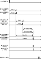
- FIG. 3 is a timing chart in the laser system shown in FIG.
- FIG. 4 is a timing chart showing a specific correction method in the nth trigger correction unit.
- FIG. 5 is a flowchart showing processing of the laser system control unit shown in FIG.
- FIG. 6 is a flowchart showing processing of the laser control unit shown in FIG.
- FIG. 7 is a flowchart showing the processing of the nth trigger correction unit shown in FIG.
- FIG. 1 schematically shows a configuration of a laser annealing apparatus including a laser system according to a comparative example.
- FIG. 2 shows a configuration example of the laser system shown in FIG.
- FIG. 3 is a timing chart in the laser system shown in FIG.
- FIG. 4 is a timing chart showing a specific correction method in the nth trigger
- FIG. 8 schematically illustrates the configuration of the laser system according to the first embodiment of the present disclosure.
- FIG. 9 shows an internal configuration of the laser chamber as viewed from a direction substantially parallel to the traveling direction of the pulse laser beam in the first embodiment.
- FIG. 10 is a flowchart showing processing of the measurement control unit shown in FIG.
- FIG. 11 is a flowchart showing processing of the bleed circuit control unit shown in FIG.
- FIG. 12 schematically illustrates a configuration of a laser system according to the second embodiment of the present disclosure.
- FIG. 13 schematically illustrates a configuration of a laser system according to the third embodiment of the present disclosure.
- FIG. 14 schematically illustrates a configuration of a laser system according to the fourth embodiment of the present disclosure.
- FIG. 10 is a flowchart showing processing of the measurement control unit shown in FIG.
- FIG. 11 is a flowchart showing processing of the bleed circuit control unit shown in FIG.
- FIG. 12 schematically illustrates a configuration of a laser system according to the second embodiment
- FIG. 15 schematically illustrates a configuration of a laser system according to the fifth embodiment of the present disclosure.
- FIG. 16 schematically shows a configuration of the bleed circuit 79 shown in FIG.
- FIG. 17 schematically illustrates a configuration of a laser system according to the sixth embodiment of the present disclosure.
- FIG. 18 is a block diagram illustrating a schematic configuration of the control unit.
- FIG. 1 schematically shows the configuration of a laser annealing apparatus including a laser system according to a comparative example.
- the laser annealing apparatus 1 shown in FIG. 1 may include a laser system 5 and an annealing apparatus 4.
- the laser system 5 may include a laser system control unit 20, a synchronization control unit 22, first and second laser devices 2 a and 2 b, and a beam splitter 3.
- Each of the first and second laser devices 2a and 2b may be an excimer laser device using, for example, XeF, XeCl, KrF, or ArF as a laser medium.
- the first and second laser devices 2a and 2b may have substantially the same configuration.
- the first and second laser devices 2a and 2b may output first and second pulse laser beams 21a and 21b, respectively.
- the first and second pulse laser beams 21a and 21b may have an ultraviolet wavelength region.
- the first and second pulsed laser beams 21a and 21b may be guided to the beam splitter 3. Although two laser devices are shown in FIG. 1, the number of laser devices is not particularly limited, and may be three or more as will be described later with reference to FIG.
- the luminous device 3 may include high reflection mirrors 31 and 32 and a right-angle prism 33.
- a right angle prism 33 may be disposed between the high reflection mirrors 31 and 32.
- the high reflection mirror 31 may be disposed so as to intersect with the optical path axis of the first pulse laser beam 21a at an angle of about 45 °.
- the high reflection mirror 32 may be disposed so as to intersect the optical path axis of the second pulse laser beam 21b at an angle of about 45 °.
- the right-angle prism 33 may be formed in a triangular prism shape whose bottom surface, which is a plane parallel to the paper surface, is a right-angle triangle. High reflection films may be coated on the two side surfaces forming the right angle of the right-angle prism 33. Two side surfaces forming a right angle of the right-angle prism 33 may constitute a first reflection surface 33a and a second reflection surface 33b, respectively.
- the first pulse laser beam 21a output from the first laser device 2a may be reflected by the high reflection mirror 31 toward the first reflection surface 33a of the right-angle prism 33. Further, the first pulse laser beam 21 a may be reflected by the first reflecting surface 33 a of the right-angle prism 33 and output toward the annealing device 4.
- the second pulse laser beam 21b output from the second laser device 2b may be reflected by the high reflection mirror 32 toward the second reflection surface 33b of the right-angle prism 33. Further, the second pulse laser beam 21 b may be reflected by the second reflecting surface 33 b of the right-angle prism 33 and output toward the annealing device 4.
- the light beam splitter 3 makes the first and second pulse laser beams 21 a and 21 b have their optical path axes parallel to each other and closes these optical paths to form the light beam laser beam 21. It may be emitted.
- the “optical path axis” of the pulse laser beam means the central axis of the optical path of the pulse laser beam.
- Flued laser beam may be a pulsed laser beam in which a plurality of pulsed laser beams are bundled.
- the light beam laser beam 21 may have about twice as much pulse energy as the pulse laser beam output from one laser device.
- the annealing apparatus 4 may include an annealing control unit 40, an illumination optical system 42, a mask 43, a high reflection mirror 41, a transfer optical system 44, and a stage 45.
- the annealing device 4 may form the luminous laser beam 21 emitted from the laser system 5 into a predetermined mask pattern and transfer the mask pattern to the irradiation object P.
- the illumination optical system 42 includes a fly-eye lens 421 and a condenser optical system 422, and may be designed to constitute Koehler illumination.
- the fly eye lens 421 may be disposed in the optical path of the light beam laser beam 21 emitted from the laser system 5.
- the fly-eye lens 421 may include a plurality of lenses arranged along the cross section of the light beam laser beam 21.
- the luminous laser beam 21 incident on the fly-eye lens 421 may be substantially parallel light.
- Each of the plurality of lenses included in the fly-eye lens 421 may enlarge the beam width of each part of the light flux laser beam 21 when transmitting the part of the light flux laser beam 21 toward the condenser optical system 422.
- the condenser optical system 422 may be disposed in the optical path of the light beam laser beam 21 emitted from the fly-eye lens 421.
- the condenser optical system 422 may illuminate the light beam laser beam 21 emitted from the fly-eye lens 421 toward the mask 43.
- the condenser optical system 422 may be arranged so that the position of the rear focal plane of the condenser optical system 422 substantially coincides with the position of the mask 43. Therefore, the condenser optical system 422 can make the luminous laser beams 21 transmitted through each of the plurality of lenses included in the fly-eye lens 421 enter substantially the same region of the mask 43.
- the condenser optical system 422 is illustrated as including one convex lens, but may include a combination with another convex lens or a concave lens (not illustrated), a concave mirror, or the like.
- the illumination optical system 42 can reduce variation in the light intensity distribution in the beam cross section of the light beam laser beam 21 irradiated on the mask 43.
- the mask 43 may be a slit in which a rectangular opening is formed.
- the opening shape of the slit can constitute a mask pattern of the mask 43.
- the mask pattern of the mask 43 is not limited to a rectangular shape, and may be a pattern having a desired shape.
- the high reflection mirror 41 may be disposed in the optical path of the light beam laser beam 21 that has passed through the mask 43.
- the high reflection mirror 41 may reflect the light beam laser beam 21 so as to enter the transfer optical system 44.
- the transfer optical system 44 may be disposed in the optical path of the light beam laser beam 21 reflected by the high reflection mirror 41.
- the transfer optical system 44 may be arranged so that the position of the image of the mask 43 formed by the transfer optical system 44 substantially coincides with the irradiated position of the irradiated object P. Thereby, the transfer optical system 44 can transfer the mask pattern of the mask 43 to the irradiated object P.
- the transfer optical system 44 may include one or more convex lenses.
- the transfer optical system 44 is not limited to one or a plurality of convex lenses, and may include, for example, a combination of a convex lens and a concave lens, a concave mirror, or the like.
- the transfer optical system 44 may be configured by a cylindrical lens that transfers only the short direction of the rectangular mask pattern to the irradiation object P.
- the stage 45 may be configured to move the irradiated object P so that the image of the mask 43 formed by the transfer optical system 44 scans the irradiated surface of the irradiated object P.
- the laser system 5 can output the luminous laser beam 21 having higher pulse energy than the pulse laser beam output from one laser device.
- the laser annealing apparatus 1 can irradiate the irradiated object P with the luminous laser beam 21 with a predetermined pulse energy density required for annealing and a wide irradiation area. And it may be possible to efficiently manufacture a large area liquid crystal display.
- the annealing control unit 40 may perform control such as movement of the stage 45 and replacement of the irradiation object P and the mask 43.
- the annealing control unit 40 may output a trigger signal TR to the laser system control unit 20.
- the laser system control unit 20 may transmit the trigger signal TR received from the annealing control unit 40 to the synchronization control unit 22. Based on the trigger signal TR received from the laser system control unit 20, the synchronization control unit 22 sends the first and second switch signals S (1) and S (2) to the first and second laser devices 2a and 2a, respectively. You may transmit to 2b. The first and second laser devices 2 a and 2 b may output pulsed laser light based on the respective switch signals received from the synchronization control unit 22.
- FIG. 2 shows a configuration example of the laser system shown in FIG.
- the first laser device 2a may include a laser chamber 10, a pair of electrodes 11a and 11b, a charger 12, and a pulse power module (PPM) 13.
- the first laser device 2a may further include a high reflection mirror 14, an output coupling mirror 15, a pulse energy measurement unit 17, a discharge sensor 18, and a laser control unit 19.
- the configuration of the second laser device 2b may be the same.
- FIG. 2 shows the internal configuration of the laser chamber 10 as viewed from the direction perpendicular to both the traveling direction of the pulsed laser light 21a and the discharge direction between the pair of electrodes 11a and 11b.
- the laser chamber 10 may be a chamber in which a laser gas as a laser medium containing, for example, argon, krypton, or xenon as a rare gas, neon or helium as a buffer gas, chlorine, fluorine, or the like as a halogen gas is enclosed.
- the pair of electrodes 11a and 11b may be disposed in the laser chamber 10 as electrodes for exciting the laser medium by discharge.
- An opening may be formed in the laser chamber 10, and the opening may be closed by the electrical insulating portion 29.
- the electrode 11a may be supported by the electrical insulating portion 29, and the electrode 11b may be supported by the return plate 10d.
- the return plate 10d may be connected to the inner surface of the laser chamber 10 by wirings 10e and 10f described later with reference to FIG.
- the electrically insulating portion 29 may be embedded with a conductive portion 29a.
- the conductive part 29a may apply a high voltage supplied from the pulse power module 13 to the electrode 11a.
- the charger 12 may be a DC power supply that charges a charging capacitor C0 (described later) in the pulse power module 13 with a predetermined voltage.
- the pulse power module 13 may include a switch 13a and a magnetic compression circuit described later.
- the pulse power module 13 may correspond to the pulse generator of the present disclosure.
- the high reflection mirror 14 and the output coupling mirror 15 may constitute an optical resonator.
- the pulse energy measurement unit 17 may include a beam splitter 17a, a condensing optical system 17b, and an optical sensor 17c.
- the synchronization control unit 22 may include first and second trigger correction units 22a and 22b and a delay circuit unit 24.
- Each of the first and second trigger correction units 22 a and 22 b may include a processing unit 25, a delay circuit 26, and a timer 27.
- a common clock signal is supplied to the first and second trigger correction units 22a and 22b and the delay circuit unit 24 by a clock generator (not shown). Also good.
- the delay circuit unit 24 may receive the trigger signal TR output from the laser system control unit 20.
- the delay circuit unit 24 uses the first delay signal TR (1) indicating that the first delay time TRd (1) has elapsed since the reception of the trigger signal TR as a delay circuit of the first trigger correction unit 22a. 26 and the timer 27 may be output.
- the delay circuit unit 24 uses the second delay signal TR (2) indicating that the second delay time TRd (2) has elapsed since the reception of the trigger signal TR as a delay circuit of the second trigger correction unit 22b. 26 and the timer 27 may be output.
- the data of the first delay time TRd (1) and the data of the second delay time TRd (2) may be given from the laser system control unit 20 to the synchronization control unit 22.
- the delay circuit 26 of the first trigger correction unit 22a receives the first switch signal S (1) indicating that the first correction time Td (1) has elapsed since the reception of the first delay signal TR (1). ) May be output to the pulse power module 13 of the first laser device 2a.
- the first correction time Td (1) may be set by the processing unit 25 of the first trigger correction unit 22a.
- the delay circuit 26 of the second trigger correction unit 22b receives the second switch signal S (2) indicating that the second correction time Td (2) has elapsed since the reception of the second delay signal TR (2). ) May be output to the pulse power module 13 of the second laser device 2b.
- the second correction time Td (2) may be set by the processing unit 25 of the second trigger correction unit 22b.
- the laser control unit 19 may send and receive various signals to and from the laser system control unit 20 described above.
- the laser control unit 19 may receive target pulse energy data from the laser system control unit 20.
- the laser controllers 19 of the first and second laser devices 2a and 2b set the charging voltage based on the target pulse energy Et (1) and Et (2) data received from the laser system controller 20, respectively.
- the values V (1) and V (2) may be calculated.
- the laser control unit 19 may transmit the set value of the charging voltage to the charger 12 and the processing unit 25 of the corresponding trigger correction unit. .
- the charger 12 may charge the charging capacitor C0 in the pulse power module 13 according to the set value of the charging voltage.
- the pulse power modules 13 of the first and second laser devices 2a and 2b may receive the first and second switch signals S (1) and S (2) output from the delay circuit 26, respectively. .
- the switch 13a of the pulse power module 13 of the first and second laser devices 2a and 2b may be switched from OFF to ON by switch signals S (1) and S (2), respectively.
- the pulse power module 13 when the switch 13a is turned from OFF to ON, the pulse power module 13 generates a pulsed high voltage from the electric energy held in the charging capacitor C0. Also good. This high voltage may be applied to the pair of electrodes 11a and 11b.
- the laser medium in the laser chamber 10 can be excited to shift to a high energy level.
- the excited laser medium subsequently moves to a low energy level, light corresponding to the energy level difference can be emitted.
- the light generated in the laser chamber 10 can be emitted to the outside of the laser chamber 10 through the windows 10a and 10b.
- the high reflection mirror 14 may reflect the light emitted from the window 10 a of the laser chamber 10 with a high reflectance and return it to the laser chamber 10.
- the output coupling mirror 15 may transmit a part of the light output from the window 10 b of the laser chamber 10 and output it, and may reflect the other part and return it to the laser chamber 10.
- the light emitted from the laser chamber 10 reciprocates between the high reflection mirror 14 and the output coupling mirror 15, and can be amplified every time it passes through the laser gain space between the electrode 11a and the electrode 11b.
- each part of the amplified light can be output as pulsed laser light 21 a and 21 b via the output coupling mirror 15.
- the beam splitter 17a of the pulse energy measuring unit 17 may transmit the pulse laser beam with high transmittance and reflect a part of the pulse laser beam toward the condensing optical system 17b.
- the condensing optical system 17b may condense the pulse laser beam reflected by the beam splitter 17a on the light receiving surface of the optical sensor 17c.
- the optical sensor 17 c may detect the pulse energy of the pulsed laser light focused on the light receiving surface and output data of the detected pulse energy to the laser control unit 19.
- the laser controller 19 may feedback control the set value of the charging voltage based on the target pulse energy data received from the laser system controller 20 and the detected pulse energy data.
- the discharge sensors 18 of the first and second laser devices 2a and 2b detect the discharge generated between the pair of electrodes 11a and 11b, and the first and second discharge detection signals DS (1) and DS (2), respectively. ) May be output.
- the first and second discharge detection signals DS (1) and DS (2) may be input to the timers 27 of the first and second trigger correction units 22a and 22b, respectively.
- the timer 27 of the first trigger correction unit 22a receives a first elapsed time TRdm (from the time when the first delay signal TR (1) is received until the time when the first discharge detection signal DS (1) is received. 1) may be measured and transmitted to the processing unit 25.
- the timer 27 of the second trigger correction unit 22b receives a second elapsed time TRdm (from when the second delay signal TR (2) is received until when the second discharge detection signal DS (2) is received. 2) may be measured and transmitted to the processing unit 25.
- the processing unit 25 of the first trigger correction unit 22a includes the charging voltage set value V (1) transmitted from the laser control unit 19 of the first laser apparatus 2a and the first elapsed time transmitted from the timer 27. Based on TRdm (1), the first correction time Td (1) may be set.
- the processing unit 25 of the second trigger correction unit 22b includes the charging voltage set value V (2) transmitted from the laser control unit 19 of the second laser apparatus 2b and the second elapsed time transmitted from the timer 27. Based on TRdm (2), the second correction time Td (2) may be set.
- FIG. 3 is a timing chart in the laser system shown in FIG.
- the laser system control unit 20 may transmit the trigger signal TR received from the annealing control unit 40 to the synchronization control unit 22.
- the delay circuit unit 24 of the synchronization control unit 22 may output the first and second delay signals TR (1) and TR (2) to the first and second trigger correction units 22a and 22b, respectively.
- the first and second delay signals may each indicate that different first and second delay times TRd (1) and TRd (2) have elapsed since the trigger signal TR was received.
- the time from the output timing of the first and second delay signals TR (1) and TR (2) to the output timing of the first and second discharge detection signals DS (1) and DS (2) is almost equal to each other. It is desirable to be controlled to be equal. In that case, the first and second discharge detection signals DS (1) and DS (2) are output with substantially the same time difference as the time difference between the first and second delay signals TR (1) and TR (2). Can be done.
- the first and second pulse laser beams 21a and 21b may be output from the first and second laser devices 2a and 2b, respectively.
- the first and second pulse laser beams 21a and 21b may be output at substantially the same timing as the first and second discharge detection signals DS (1) and DS (2), respectively.
- the first and second pulse laser beams 21a and 21b may be output at timing slightly delayed from the first and second discharge detection signals DS (1) and DS (2), respectively.
- the optical path lengths from the respective output positions of the first and second laser devices 2a and 2b to the emission position of the beam forming device 3 may be adjusted to be substantially equal to each other.
- the light flux laser beam 21 emitted from the light flux generator 3 has the first and second pulses having the same time difference as the time difference between the first and second delay signals TR (1) and TR (2).
- the laser beams 21a and 21b may be combined. By controlling the timing of the first and second delay signals TR (1) and TR (2), the pulse waveform of the light beam laser beam 21 can be adjusted.
- the first delay signal TR (1) and the second delay signal TR (2) may have a predetermined time difference.
- the first required time from the time when the first laser device 2a receives the first switch signal S (1) to the time when the first pulse laser beam is generated is the first laser device 2a. It may vary depending on the charging voltage charged in the charging capacitor C0.
- the second required time from the time when the second laser device 2b receives the second switch signal S (2) to the time when the second pulse laser beam is generated is the charging capacitor C0 of the second laser device 2b. It may vary depending on the charging voltage charged.
- These charging voltages can be controlled separately by the first laser device 2a and the second laser device 2b. Accordingly, the first required time and the second required time can vary separately from each other.
- the first required time and the second required time can vary depending on the temperature of the magnetic compression circuit included in each pulse power module 13.
- the first elapsed time TRdm (1) from the time when the timer 27 receives the first delay signal TR (1) to the time when the first discharge detection signal DS (1) is received is the first correction time. It may correspond to the total time of Td (1) and the first required time.
- the second elapsed time TRdm (2) from the time when the timer 27 receives the second delay signal TR (2) to the time when the second discharge detection signal DS (2) is received is the second correction time. It may correspond to the total time of Td (2) and the second required time.
- the first pulsed laser beam 21a and the second pulsed laser beam 21b can be generated with substantially the same time difference.
- FIG. 4 is a timing chart showing a specific correction method in the nth trigger correction unit.
- each of the first and second trigger correction units 22a and 22b may be referred to as an nth trigger correction unit 22n.
- the signal input or output by the nth trigger correction unit 22n is indicated with (n), or the time set in the nth trigger correction unit 22n is indicated with (n). is there.
- the nth correction time Td (n) may be calculated by the following equation.
- Td (n) Td0 (n) + ⁇ TV (n)
- Td0 (n) may be the first correction element
- ⁇ TV (n) may be the second correction element.
- the initial value of the first correction element Td0 (n) may be set by the following equation.
- Initial value of Td0 (n) TRdt ⁇ F (V0 (n))
- TRdt may be a target value of the nth elapsed time TRdm (n).
- the nth elapsed time TRdm (n) is an elapsed time from when the timer 27 receives the nth delay signal TR (n) to when the timer 27 receives the nth discharge detection signal DS (n). Also good.
- the target value TRdt of the nth elapsed time TRdm (n) is a value common to the first and second trigger correction units 22a and 22b will be described, but different target values are set. You may do it.
- F (V0 (n)) is the nth switch signal S (n) when the set value of the charging voltage in the nth laser device 2n is a predetermined reference voltage value V0 (n). May be a calculated value of a required time from the input of n to the output of the nth discharge detection signal DS (n).
- the product of the required time T until the voltage is applied between the pair of electrodes 11a and 11b can be a substantially constant value K. Accordingly, the calculation of F (V0 (n)) may be performed by the following equation.
- F (V0 (n)) K / V0 (n) V0 (n) may be a reference voltage value.
- the second correction element ⁇ TV (n) is expressed by the following equation: It may be calculated.
- ⁇ TV (n) F (V0 (n)) ⁇ F (V (n))
- F (V (n)) is the nth discharge from the input of the nth switch signal S (n) when the set value of the charging voltage in the nth laser device 2n is V (n). It may be a calculated value of the time required until the output of the detection signal DS (n).
- the calculation of F (V (n)) may be performed by the following equation.
- F (V (n)) K / V (n)
- the timing control of the nth switch signal S (n) is performed at high speed. Can do.
- the processing unit 25 of the nth trigger correction unit 22n receives the nth discharge detection signal DS (n) from when the timer 27 receives the nth delay signal TR (n).
- the difference ⁇ TRd (n) from the target value TRdt may be calculated.
- the first correction element Td0 (n) may be updated by the following equation.
- Td0 (n) Td0 (n) ⁇ TRd (n)
- the timing control of the nth switch signal S (n) can be performed with high accuracy.
- a change in discharge timing due to a change in temperature of the magnetic compression circuit, a change in gas pressure in the laser chamber, or the like is defined as a “drift change”.
- FIG. 5 is a flowchart showing processing of the laser system control unit shown in FIG.
- the laser system control unit 20 performs the following processing on the target pulse energy Et (n) and the nth delay time TRd (n) for each of the nth pulsed laser beams 21n output from the nth laser device 2n. May be calculated.
- the laser system control unit 20 receives the target pulse waveform data of the light beam laser beam 21 and the target pulse energy data of the light beam laser beam 21 from the annealing control unit 40 of the annealing device 4. May be.
- the laser system control unit 20 may calculate the target pulse energy Et (n) and the nth delay time TRd (n) for each of the nth pulsed laser beams 21n. For example, when the target pulse waveform of the light beam laser beam 21 has a short pulse width, each of the nth delay times TRd (n) may be a value close to each other.
- the target pulse energy Et (n) of the n-th pulse laser beam 21n is adjusted so that the total of the target pulse energy Et (n) of the n-th pulse laser beam 21n approaches the target pulse energy of the light beam laser beam 21. n) may be determined.
- the laser system control unit 20 may transmit the respective values to the laser control unit 19 of the corresponding laser device. After calculating the nth delay time TRd (n) for each of the nth pulse laser beams 21n, the laser system control unit 20 may transmit these values to the delay circuit unit 24 of the synchronization control unit 22. .
- the laser system control unit 20 may determine whether or not to change the target pulse waveform of the luminous laser beam 21 and the target pulse energy of the luminous laser beam 21. When changing these values (S113; YES), the laser system control unit 20 may return the process to S102 described above. When not changing (S113; NO), the laser system control part 20 may advance a process to S114.
- the laser system control unit 20 may determine whether or not to stop the control of the pulse waveform.
- the laser system control unit 20 may return the process to S113 described above.
- the laser system control unit 20 may end the process of this flowchart.
- the laser system control unit 20 may calculate the target pulse energy Et (n) and the nth delay time TRd (n).
- FIG. 6 is a flowchart showing processing of the laser control unit shown in FIG.
- the laser control unit 19 included in each of the nth laser devices 2n may calculate the set value V (n) of the charging voltage based on the target pulse energy Et (n) by the following process.
- the laser control unit 19 may set the setting value V (n) of the charging voltage of the laser device 2n to an initial value.
- the initial value of the setting value of the charging voltage may be the above-described reference voltage value V0 (n).
- the laser control unit 19 may read the target pulse energy Et (n) of the laser device 2 (n) from the laser system control unit 20.
- the laser control unit 19 may determine whether or not the laser device 2 (n) oscillates. When the laser device 2 (n) does not oscillate (S203; NO), the laser control unit 19 may stand by until laser oscillation occurs. When the laser apparatus 2 (n) performs laser oscillation (S203; YES), the laser control unit 19 may advance the process to S204.
- the laser control unit 19 may detect the pulse energy E (n) of the pulsed laser light 21n output from the laser device 2n.
- the pulse energy E (n) may be detected by the pulse energy measuring unit 17.
- the laser control unit 19 may calculate a difference ⁇ E (n) between the detected pulse energy E (n) and the target pulse energy Et (n) by the following equation.
- ⁇ E (n) E (n) ⁇ Et (n)
- the laser control unit 19 may calculate the change amount ⁇ V (n) of the set value of the charging voltage based on the difference ⁇ E (n) from the target pulse energy by the following equation.
- ⁇ V (n) H ⁇ ⁇ E (n)
- H may be a proportionality constant.
- the amount of change ⁇ V (n) in the setting value of the charging voltage may indicate how much the setting value V (n) of the next charging voltage should be changed.
- the laser control unit 19 may calculate the set value V (n) of the next charging voltage using the following equation.
- V (n) V (n) + ⁇ V (n)
- the laser control unit 19 may transmit the set value V (n) of the next charging voltage to the charger 12 and the processing unit 25 of the nth trigger correction unit 22n.
- the laser control unit 19 may determine whether or not to change the target pulse energy Et (n).
- the laser control unit may return the process to S202 described above.
- the target pulse energy Et (n) is not changed (S208; NO)
- the laser control unit may return the process to S203 described above.
- the laser control unit 19 may calculate the set value V (n) of the charging voltage.
- FIG. 7 is a flowchart showing the process of the nth trigger correction unit shown in FIG.
- the nth trigger correction unit 22n may calculate the first correction element Td0 (n) and the second correction element ⁇ TV (n) constituting the nth correction time Td (n) by the following process. Good.
- J may be a counter for counting the number of oscillation pulses.
- TRdmsum (n) is an nth elapsed time TRdm (n) from the time when the timer 27 receives the nth delay signal TR (n) to the time when the nth discharge detection signal DS (n) is received. It may be a total value of TRdm (n) for calculating an average value.
- Td0 (n) may be a first correction element
- TRdt-F (V0 (n)) may be an initial value of the first correction element described above.
- the nth trigger correction unit 22n may read the set value V (n) of the charging voltage from the laser control unit 19.
- the nth trigger correction unit 22n may calculate the second correction element ⁇ TV (n) by the following equation based on the set value V (n) of the charging voltage.
- ⁇ TV (n) F (V0 (n)) ⁇ F (V (n))
- the nth trigger correction unit 22n may calculate the nth correction time Td (n) by the following equation.
- Td (n) Td0 (n) + ⁇ TV (n)
- Td0 (n) may be a first correction element
- ⁇ TV (n) may be a second correction element.
- the nth trigger correction unit 22n may determine whether or not the nth laser device 2n has oscillated. Whether or not the nth laser device 2n has oscillated may be determined by whether or not the timer 27 has received the nth discharge detection signal DS (n) from the discharge sensor 18.
- the nth trigger correction unit 22n may advance the process to S307.
- the n-th trigger correction unit 22n may stand by until the n-th laser device 2n oscillates.
- the nth trigger correction unit 22n may update the value of J by adding 1 to the current value of the counter J.
- the nth trigger correction unit 22n performs the operation from the time when the timer 27 receives the nth delay signal TR (n) to the time when the nth discharge detection signal DS (n) is received.
- the elapsed time TRdm (n) of n may be read from the timer 27.
- the nth trigger correction unit 22n may update the total value TRdmsum (n) of TRdm (n) by the following equation.
- TRdmsum (n) TRdmsum (n) + TRdm (n)
- the nth trigger correction unit 22n may determine whether or not the value of the counter J has reached a predetermined number of samples Jmax. When the value of the counter J has not reached the predetermined number of samples Jmax (S312; NO), the nth trigger correction unit 22n may return the process to S302 described above. When the value of the counter J reaches the predetermined number of samples Jmax (S312; YES), the nth trigger correction unit 22n may advance the process to S313.
- the nth trigger correction unit 22n may calculate a difference ⁇ TRd (n) between the average value of TRdm (n) and the target value TRdt.
- the nth trigger correction unit 22n may update the first correction element Td0 (n) by the following equation.
- Td0 (n) Td0 (n) ⁇ TRd (n)
- the nth trigger correction unit 22n may return the process to S302 described above.
- the nth trigger correction unit 22n calculates the nth correction time Td (n) while updating the first correction element Td0 (n) and the second correction element ⁇ TV (n). May be.
- the second correction element ⁇ TV (n) may be updated for each pulse oscillation as described above.
- the first correction element Td0 (n) may be updated for each pulse oscillation of the predetermined number of samples Jmax.
- the predetermined number of samples Jmax may be, for example, 200 to 10,000 times.
- the frequency of the setting process for setting the nth correction time Td (n) by updating the first correction element Td0 (n) is the nth correction by updating the second correction element ⁇ TV (n). It may be smaller than the frequency of the setting process for setting the time Td (n).
- the nth trigger correction unit 22n corrects the nth correction time Td (n) according to the fluctuation of the nth required time, whereby the nth elapsed time TRdm (n ) Can be made closer to the target value TRdt. Specifically, it is possible to control the correction time based on the set value of the charging voltage and to control the correction time according to the fluctuation of the nth required time due to the drift change. Thereby, the discharge timing of each laser device can be stabilized, and the pulse waveform of the light beam laser beam can be stabilized.
- the delay circuit unit 24 controls the pulse waveform of the light beam laser beam by controlling the nth delay time TRd (n), the control is performed separately from the control by the nth trigger correction unit 22n. Can do.
- a clock generator (not shown) generates a clock signal common to the first and second trigger correction units 22 a and 22 b and the delay circuit unit 24. Thereby, the mutual error of each delay time TRd (n) or correction time Td (n) can be reduced.
- the electrical signal can be delayed by 1 / c. c may be the speed of light. Therefore, the delay of the signal may be corrected from the length of the electric wire of each switch signal S (n) and the timing signal of each discharge sensor. Further, even if communication is performed using an optical fiber instead of wiring, a similar delay may occur, and this correction may be performed.
- the control of the pulse waveform of the light beam laser beam is realized by the delay circuit unit 24 controlling the nth delay time TRd (n).
- the control is limited to this comparative example.
- the following configuration may be used.
- a distributor that distributes the trigger signal TR from the annealing control unit 40 without delay is arranged, and each of the trigger correction units 22n corresponding to each laser device has a different target value TRdt (n). May be used to control the timing of the pulsed laser light output from each laser device.
- the laser system control unit 20, the synchronization control unit 22, and the laser control unit 19 of each laser device control the laser device, but the present disclosure is not limited to this.
- the annealing control unit 40 included in the annealing apparatus 4 may perform various controls.
- the second correction element ⁇ TV (n) may be calculated based on the set value V (n) of the charging voltage.
- the actual charging voltage charged in the charging capacitor C0 may deviate from the set value V (n) of the charging voltage.
- the synchronization accuracy of the plurality of pulse laser beams output from the plurality of laser devices may be deteriorated.
- the pulse waveform of the luminous laser beam obtained by bundling a plurality of pulse laser beams changes, which may affect the annealing performance.
- an actual charging voltage is accurately measured by a charging voltage measurement unit common to a plurality of laser apparatuses, and a bleed circuit and a trigger correction unit operate based on the measured charging voltage. You may do it.
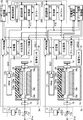
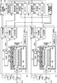
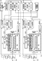
- FIG. 8 schematically illustrates a configuration of a laser system according to the first embodiment of the present disclosure.
- the overall configuration of the laser annealing apparatus 1 may be the same as that shown in FIG.
- each of the first and second laser devices 2a and 2b may further include a voltage dividing circuit 6 and a bleed circuit 7.
- the laser system 5 may further include a charging voltage measurement unit 8 and a bleed circuit control unit 9.
- the voltage dividing circuit 6 and the bleed circuit 7 may be connected to a wiring that connects the charger 12 and the charging capacitor C0 of the pulse power module 13.
- the voltage dividing circuit 6 included in each of the first and second laser devices 2 a and 2 b may be connected to the charging voltage measuring unit 8.
- the charging voltage measurement unit 8 may be connected to the bleed circuit control unit 9.
- the bleed circuit control unit 9 may be connected to a signal line that connects the laser control unit 19 of the first and second laser devices 2a and 2b and the processing unit 25 of the trigger correction unit corresponding to these laser devices. .
- the bleed circuit control unit 9 may be further connected to a bleed circuit 7 included in each of the first and second laser devices 2a and 2b.
- FIG. 9 shows the internal configuration of the laser chamber as viewed from a direction substantially parallel to the traveling direction of the pulse laser beam in the first embodiment.
- FIG. 9 also shows the configuration of the pulse power module, discharge sensor, voltage dividing circuit, bleed circuit, and charging voltage measuring instrument shown in FIG.
- the conductive member including the wall surface of the laser chamber 10 may be connected to a ground potential.
- the electrode 11b may be connected to the ground potential via the return plate 10d, the wirings 10e and 10f, and the wall surface of the laser chamber 10.
- the discharge sensor 18 included in each of the first and second laser devices 2a and 2b may include a window 10c attached to the laser chamber 10, a condensing optical system 181, and an optical sensor 182.
- the window 10c may transmit light generated by the discharge between the pair of electrodes 11a and 11b.
- the condensing optical system 181 may condense the light transmitted through the window 10 c on the light receiving surface of the optical sensor 182.
- the optical sensor 182 may include a photodiode or a phototube.
- the optical sensor 182 may transmit the nth discharge detection signal DS (n) indicating the discharge timing to the synchronization control unit 22 by detecting light generated by the discharge between the pair of electrodes 11a and 11b. .
- the pulse power module 13 may include a charging capacitor C0, a switch 13a, a step-up transformer TC1, a plurality of magnetic switches Sr1 to Sr3, and a plurality of capacitors C1 to C3.
- the step-up transformer TC1, the plurality of magnetic switches Sr1 to Sr3, and the plurality of capacitors C1 to C3 may constitute a magnetic compression circuit.
- any of the magnetic switches Sr1 to Sr3 may include a saturable reactor.
- Each of the magnetic switches Sr1 to Sr3 may have a low impedance when the time integration value of the voltage applied to both ends thereof reaches a predetermined value determined by the characteristics of each magnetic switch.
- a charging voltage set value V (n) may be set in the charger 12 by the laser controller 19.
- the charger 12 may charge the charging capacitor C0 based on the set value V (n) of the charging voltage.
- a switch signal may be input to the switch 13 a of the pulse power module 13 by the synchronization control unit 22. When the switch signal is input to the switch 13a, the switch 13a may be turned on. When the switch 13a is turned on, a current can flow from the charging capacitor C0 to the primary side of the step-up transformer TC1.
- the magnetic switch Sr1 When the time integral value of the voltage applied to the magnetic switch Sr1 reaches a threshold value, the magnetic switch Sr1 becomes magnetically saturated and the magnetic switch Sr1 can be closed. When the magnetic switch Sr1 is closed, a current flows from the secondary side of the step-up transformer TC1 to the capacitor C1, and the capacitor C1 can be charged.
- the magnetic switch Sr2 When the capacitor C1 is charged, the magnetic switch Sr2 eventually becomes magnetically saturated and the magnetic switch Sr2 can be closed. When the magnetic switch Sr2 is closed, a current flows from the capacitor C1 to the capacitor C2, and the capacitor C2 can be charged. At this time, the capacitor C2 may be charged with a pulse width shorter than the pulse width of the current when the capacitor C1 is charged.
- the magnetic switch Sr3 When the capacitor C2 is charged, the magnetic switch Sr3 eventually becomes magnetically saturated and the magnetic switch Sr3 can be closed. When the magnetic switch Sr3 is closed, a current flows from the capacitor C2 to the capacitor C3, and the capacitor C3 can be charged. At this time, the capacitor C3 may be charged with a pulse width shorter than the pulse width of the current when the capacitor C2 is charged.
- the pulse width of the current can be compressed by sequentially flowing the current from the capacitor C1 to the capacitor C2 and from the capacitor C2 to the capacitor C3.
- the pulse laser beam may be output at a predetermined oscillation frequency.
- a discharge timing detector instead of the discharge sensor 18, an ammeter 18b for detecting a discharge current may be used. This ammeter 18b is a current probe, and may detect the timing of discharge.
- the pulse energy measuring unit 17 (FIG. 8) may be used as a discharge timing detector instead of the discharge sensor 18.
- the pulse energy measuring unit 17 may include a high-speed photodiode.
- the voltage dividing circuit 6 included in each of the first and second laser devices 2a and 2b may include a first resistance element 61 and a second resistance element 62.
- the first resistance element 61 may be connected to a wiring that connects the charger 12 and the charging capacitor C0 of the pulse power module 13.
- the second resistance element 62 may be connected between the first resistance element 61 and the ground potential.
- An output terminal 63 between the first resistance element 61 and the second resistance element 62 may be connected to the charging voltage measurement unit 8.
- the first resistance element 61 may have a resistance value ten times or more that of the second resistance element 62.
- the voltage of the output terminal 63 is a voltage obtained by dividing the charging voltage charged in the charging capacitor C0 at a ratio corresponding to the resistance ratio between the first resistance element 61 and the second resistance element 62. Also good.
- the charging voltage measurement unit 8 may include a first amplifier 81, a second amplifier 82, a multiplexer 83, an AD converter 84, and a measurement control unit 85.
- the first amplifier 81 may amplify the voltage signal output from the voltage dividing circuit 6 included in the first laser device 2 a and output the amplified voltage signal to the first channel of the multiplexer 83.
- the second amplifier 82 may amplify the voltage signal output from the voltage dividing circuit 6 included in the second laser device 2 b and output the amplified voltage signal to the second channel of the multiplexer 83.
- the multiplexer 83 may be further connected to the AD converter 84.
- the multiplexer 83 is a switch that can be switched between a first mode in which the output of the first amplifier 81 is input to the AD converter 84 and a second mode in which the output of the second amplifier 82 is input to the AD converter 84. There may be.
- the AD converter 84 may convert the analog voltage signal input from the multiplexer 83 into digital voltage data and output the digital voltage data to the measurement control unit 85.
- the AD converter 84 may be a common measurement unit connected to the multiplexer 83.
- the measurement control unit 85 may be connected to the multiplexer 83 and the AD converter 84 via signal lines, respectively, and control the multiplexer 83 and the AD converter 84.
- the measurement control unit 85 may output the voltage data received from the AD converter 84 to the bleed circuit control unit 9.
- the bleed circuit control unit 9 sets the charging voltage setting value V (1) set by the laser control unit 19 of the first laser device 2a and the charging of the first laser device 2a measured by the charging voltage measurement unit 8.
- the charging voltage Vm (1) charged in the capacitor C0 may be compared.
- the bleed circuit control unit 9 may output a switch ON signal to the bleed circuit 7 of the first laser device 2a based on the comparison result.
- the bleed circuit control unit 9 sets the charging voltage set value V (2) set by the laser control unit 19 of the second laser device 2b and the charging of the second laser device 2b measured by the charging voltage measurement unit 8.
- the charging voltage Vm (2) charged in the capacitor C0 may be compared.
- the bleed circuit control unit 9 may output a switch ON signal to the bleed circuit 7 of the second laser device 2b based on the comparison result.
- the bleed circuit 7 included in each of the first and second laser devices 2a and 2b may include a resistance element 71 and a bipolar transistor 72.
- a resistance element 71 is connected to the wiring connecting the charger 12 and the charging capacitor C0 of the pulse power module 13, and a solid state switch such as a bipolar transistor 72 is connected between the resistance element 71 and the ground potential. May be connected.
- the terminal connected to the resistance element 71 may be a collector terminal.
- the terminal connected to the ground potential may be an emitter terminal.
- a bipolar transistor 72 is connected to the wiring connecting the charger 12 and the charging capacitor C0 of the pulse power module 13, and the resistance element 71 is connected between the resistance element 71 and the ground potential. It may be connected.
- the above-described switch ON signal output from the bleed circuit control unit 9 may be input to the base terminal of the bipolar transistor 72.
- the bipolar transistor 72 when the switch ON signal is not input to the base terminal, the collector terminal and the emitter terminal may be substantially electrically insulated.
- the bipolar transistor 72 when a switch ON signal is input to the base terminal, the electrical resistance between the collector terminal and the emitter terminal may decrease. At this time, a current flows through the resistance element 71 and the bipolar transistor 72, and the charging voltage charged in the charging capacitor C0 of the pulse power module 13 may decrease.
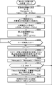
- FIG. 10 is a flowchart showing processing of the measurement control unit shown in FIG.
- the measurement control unit 85 controls the multiplexer 83 and the AD converter 84 by the following processing, and charges the charging capacitors C0 of the first and second laser devices 2a and 2b, respectively. And Vm (2) may be measured.
- the measurement control unit 85 may set the multiplexer 83 to the first channel. Accordingly, the charging capacitor C0 of the first laser device 2a may be connected to the AD converter 84 via the voltage dividing circuit 6 and the first amplifier 81.
- the measurement control unit 85 may read the charging voltage Vm (1) charged in the charging capacitor C0 of the first laser device 2a by reading the output of the AD converter 84.
- the measurement control unit 85 may transmit data of the charging voltage Vm (1) charged in the charging capacitor C0 of the first laser device 2a to the bleed circuit control unit 9.
- the measurement control unit 85 may set the multiplexer 83 to the second channel. Accordingly, the charging capacitor C0 of the second laser device 2b may be connected to the AD converter 84 via the voltage dividing circuit 6 and the second amplifier 82.
- the measurement control unit 85 may read the charging voltage Vm (2) charged in the charging capacitor C0 of the second laser device 2b by reading the output of the AD converter 84.
- the measurement control unit 85 may transmit data of the charging voltage Vm (2) charged in the charging capacitor C0 of the second laser device 2b to the bleed circuit control unit 9.
- the measurement control unit 85 may return the process to S401 described above. Through the above processing, the measurement control unit 85 may alternately measure the charging voltages charged in the charging capacitors C0 of the first and second laser devices 2a and 2b.
- FIG. 11 is a flowchart showing processing of the bleed circuit control unit shown in FIG.
- the bleed circuit control unit 9 compares the set value of the charging voltage with the charging voltage charged in the charging capacitor C0 for each of the first and second laser devices 2a and 2b by the following processing, and the bleed circuit 7 May be controlled.
- the bleed circuit control unit 9 may read the set value V (1) of the charging voltage set by the laser control unit 19 of the first laser device 2a.
- the bleed circuit control unit 9 may determine whether or not the charging of the charging capacitor C0 of the first laser device 2a is completed. Whether or not the charging of the charging capacitor C0 is completed is determined by whether or not the charging voltage Vm (1) charged in the charging capacitor C0 is higher than the charging voltage setting value V (1). Good.
- the bleed circuit control unit 9 may read data on the charging voltage Vm (1) of the charging capacitor C0 measured by the charging voltage measuring unit 8.
- the bleed circuit control unit 9 may output a switch ON signal to the bleed circuit 7 of the first laser device 2a.
- the bleed circuit control unit 9 sets the charging voltage Vm (1) of the first laser device 2a measured by the charging voltage measuring unit 8 and the set value V ( 1) may be compared.
- the charging voltage Vm (1) of the first laser device 2a measured by the charging voltage measuring unit 8 exceeds the set value V (1) of the charging voltage of the first laser device 2a (S505; NO)
- the bleed circuit control unit 9 may return the process to the above-described S503 and control the bleed circuit 7 while newly reading the charging voltage Vm (1).
- the charging voltage Vm (1) charged in the charging capacitor C0 of the first laser device 2a can further drop.
- the charging voltage Vm (1) of the first laser device 2a measured by the charging voltage measuring unit 8 is equal to or less than the set value V (1) of the charging voltage of the first laser device 2a (S505; YES)
- the bleed circuit control unit 9 may advance the process to S506.
- the bleed circuit control unit 9 may stop the switch ON signal transmitted to the bleed circuit 7 of the first laser device 2a. That is, the bleed circuit control unit 9 may switch off the bipolar transistor 72 included in the bleed circuit 7 of the first laser device 2a.
- the bleed circuit control unit 9 transmits a signal indicating that the charging of the charging capacitor C0 of the first laser device 2a is completed to the laser control unit 19 of the first laser device 2a. Good.
- the charging voltage charged in the charging capacitor C0 of the first laser device 2a may be controlled.
- the bleed circuit control unit 9 may execute the processes of S511 to S517.
- the processing of S511 to S517 may be the one in which each component of the first laser device 2a is replaced with each component of the second laser device 2b in the processing of S501 to S507 described above. By these processes, the charging voltage charged in the charging capacitor C0 of the second laser device 2b may be controlled.
- the actual charging voltage can be accurately measured by the charging voltage measuring unit common to the plurality of laser apparatuses. Since the bleed circuit operates based on this actual charging voltage, the charging voltage can be adjusted to the set value with high accuracy. Therefore, the trigger timing correction by the trigger correction unit can be performed with high accuracy.
- U.S. Pat. No. 8,238,400 discloses disposing a switch connecting the charging capacitors of two lasers in order to make the charging voltages to the charging capacitors of the two lasers coincide with each other.
- U.S. Pat. No. 6,865,210 discloses charging two charging capacitors with one charger. However, in these methods, the charging voltages of the two lasers must be the same. In these systems, two lasers must be arranged close to each other.
- the present embodiment even when the charging voltages of the two lasers are controlled separately, the respective charging voltages can be accurately measured. Moreover, even if two lasers are arranged apart from each other, the respective charging voltages can be measured with high accuracy. Therefore, the trigger timing can be adjusted with high accuracy.
- FIG. 12 schematically illustrates a configuration of a laser system according to the second embodiment of the present disclosure.
- each of the first and second laser devices 2 a and 2 b may not include the bleed circuit 7.
- the laser system 5 may not include the bleed circuit control unit 9.
- the charging voltage measurement unit 8 may be connected to the processing unit 25 included in the first trigger correction unit 22a and the processing unit 25 included in the second trigger correction unit 22b via signal lines, respectively.
- the charging voltage measuring unit 8 transmits the data of the charging voltage Vm (1) charged in the charging capacitor C0 of the first laser device 2a to the processing unit 25 included in the first trigger correcting unit 22a. May be.
- the charging voltage measurement unit 8 may transmit data on the charging voltage Vm (2) charged in the charging capacitor C0 of the second laser device 2b to the processing unit 25 included in the second trigger correction unit 22b. .
- the first and second trigger correction units 22a and 22b may correct the trigger timings of the switch signals S (1) and S (2) based on the charging voltage by the same process as in FIG. However, in the second embodiment, the trigger timing is not corrected based on the set value V (n) of the charging voltage, but the charging voltage Vm (n of the charging capacitor C0 measured by the charging voltage measuring unit 8 is used. ), The trigger timing may be corrected. About another point, it may be the same as that of 1st Embodiment.
- the actual charging voltage can be accurately measured by the charging voltage measuring unit common to the plurality of laser devices. Since the trigger correction unit operates based on the actual charging voltage, the trigger timing can be corrected with high accuracy.
- FIG. 13 schematically illustrates a configuration of a laser system according to the third embodiment of the present disclosure.
- the first trigger correction unit including the processing unit 25, the delay circuit 26, and the timer 27 is integrated with the first laser device 2a or included in the first laser device 2a. It may be.
- the second trigger correction unit including the processing unit 25, the delay circuit 26, and the timer 27 is integrated with the second laser device 2b or included in the second laser device 2b. It may be.
- a clock generator (not shown) for the first trigger correction unit and a clock generator (not shown) for the second trigger correction unit may be separate clock generators.
- the clock frequency of these clock generators is preferably 1 GHz or more.
- the third embodiment has been described with respect to the case where the trigger correction unit is integrated with the laser device in the second embodiment that does not include a bleed circuit, the present disclosure is not limited thereto.
- the trigger correction unit may be integrated with the laser device.
- FIG. 14 schematically illustrates a configuration of a laser system according to the fourth embodiment of the present disclosure.
- the charging voltage measurement unit 8 is connected to the processing unit 25 included in the first trigger correction unit 22a and the processing unit 25 included in the second trigger correction unit 22b via signal lines, respectively. It may be connected.
- the charging voltage measuring unit 8 transfers the data of the charging voltage Vm (1) charged in the charging capacitor C0 of the first laser device 2a to the bleed circuit control unit 9 and the first trigger correction unit 22a. You may transmit to both the process parts 25 contained.
- the charging voltage measuring unit 8 converts the data of the charging voltage Vm (2) charged in the charging capacitor C0 of the second laser device 2b into a processing unit included in the bleed circuit control unit 9 and the second trigger correction unit 22b. 25 may be transmitted to both.
- the bleed circuit control unit 9 may control the charging voltage Vm (n) of the charging capacitor C0 included in the first and second laser devices 2a and 2b based on the setting value V (n) of the charging voltage. .
- the first and second trigger correction units 22a and 22b may correct the trigger timings of the switch signals S (1) and S (2) based on the charging voltage by the same process as in FIG.
- the trigger timing is not corrected based on the set value V (n) of the charging voltage, but the charging voltage Vm (n of the charging capacitor C0 measured by the charging voltage measuring unit 8 is used. ), The trigger timing may be corrected. About another point, it may be the same as that of 1st Embodiment.
- the actual charging voltage can be accurately measured by the charging voltage measuring unit common to the plurality of laser devices. Since the bleed circuit operates based on this actual charging voltage, the charging voltage can be adjusted to the set value with high accuracy. Furthermore, since the trigger correction unit operates based on the actual charging voltage adjusted in the vicinity of the set value, the trigger timing can be corrected with high accuracy. And the stability of the pulse energy of the laser device can also be improved.
- FIG. 15 schematically illustrates a configuration of a laser system according to the fifth embodiment of the present disclosure.
- the bleed circuit is not provided in each of the first and second laser devices 2a and 2b, but one common bleed circuit 79 may be provided.
- FIG. 16 schematically shows a configuration of the bleed circuit 79 shown in FIG.
- the bleed circuit 79 may include a multiplexer 73, a resistance element 71, a bipolar transistor 72, and a bleed circuit control unit 9.
- the charging capacitor C0 of the first laser device 2a may be connected to the first channel of the multiplexer 73.
- the charging capacitor C0 of the second laser device 2b may be connected to the second channel of the multiplexer 73.
- the multiplexer 73 may be further connected to the resistance element 71.
- the multiplexer 73 includes a first mode in which the charging capacitor C0 of the first laser device 2a is connected to the resistance element 71, and a second mode in which the charging capacitor C0 of the second laser device 2b is connected to the resistance element 71.
- a switch that can be switched may be used.
- the bleed circuit control unit 9 may be connected to the laser control unit 19 of the first laser device 2a, and data of the set value V (1) of the charging voltage may be input from the laser control unit 19.
- the bleed circuit control unit 9 may be connected to the laser control unit 19 of the second laser device 2b, and data of the set value V (2) of the charging voltage may be input from the laser control unit 19.
- the bleed circuit control unit 9 may be further connected to a charging voltage measuring unit 8 and may be input with the charging voltage measured by the charging voltage measuring unit 8. That is, the bleed circuit control unit 9 includes data of the charging voltage Vm (1) charged in the charging capacitor C0 of the first laser device 2a and the charging voltage charged in the charging capacitor C0 of the second laser device 2b. Vm (2) data may be input.
- the bleed circuit control unit 9 may be connected to the multiplexer 73 via a signal line and control the multiplexer 73.
- the bleed circuit control unit 9 may set the multiplexer 73 to the first channel. Thereby, the charging capacitor C0 of the first laser device 2a may be connected to the bipolar transistor 72 via the resistance element 71.
- the bleed circuit control unit 9 compares the set value V (1) of the charging voltage with the charging voltage Vm (1) charged in the charging capacitor C0 of the first laser device 2a, and based on the comparison result
- the bipolar transistor 72 may be controlled. Thereby, the bleed circuit control unit 9 may adjust the charging voltage charged in the charging capacitor C0 of the first laser device 2a.
- the bleed circuit control unit 9 may set the multiplexer 73 to the second channel. Accordingly, the charging capacitor C0 of the second laser device 2b may be connected to the bipolar transistor 72 via the resistance element 71.
- the bleed circuit control unit 9 compares the set value V (2) of the charging voltage with the charging voltage Vm (2) charged in the charging capacitor C0 of the second laser device 2b, and based on the comparison result
- the bipolar transistor 72 may be controlled. Thereby, the bleed circuit control unit 9 may adjust the charging voltage charged in the charging capacitor C0 of the second laser device 2b.
- a common bleed circuit 79 may be provided in the fourth embodiment described with reference to FIG.
- the trigger timing can be synchronized with a simpler configuration.
- FIG. 17 schematically illustrates a configuration of a laser system according to the sixth embodiment of the present disclosure.
- three or more laser devices 2a to 2k may be provided.
- Three or more trigger correction units 22a to 22k may be provided corresponding to the three or more laser devices 2a to 2k.
- a voltage dividing circuit not shown in FIG. 17 and, if necessary, a bleed circuit may be provided in each of the laser devices 2a to 2k.
- the charging voltage measuring unit 8 may be provided in common for these laser devices 2a to 2k.
- FIG. 1 shows a beam forming device 3 that converts a pulse laser beam output from two laser devices into a beam, but a pulse laser beam output from three or more laser devices 2a to 2k.
- a plurality of beam splitters 3 may be combined.
- the laser annealing apparatus 1 can irradiate the irradiated object P with the luminous laser beam 21 with a predetermined pulse energy density required for annealing and a wide irradiation area. And it may be possible to efficiently manufacture a large area liquid crystal display.
- FIG. 18 is a block diagram illustrating a schematic configuration of the control unit.
- Control units such as the laser system control unit 20 and the synchronization control unit 22 in the above-described embodiments may be configured by general-purpose control devices such as a computer and a programmable controller. For example, it may be configured as follows.
- the control unit includes a processing unit 1000, a storage memory 1005, a user interface 1010, a parallel I / O controller 1020, a serial I / O controller 1030, A / D, and D / A connected to the processing unit 1000. And a converter 1040. Further, the processing unit 1000 may include a CPU 1001, a memory 1002 connected to the CPU 1001, a timer 1003, and a GPU 1004.
- the processing unit 1000 may read a program stored in the storage memory 1005.
- the processing unit 1000 may execute the read program, read data from the storage memory 1005 in accordance with execution of the program, or store data in the storage memory 1005.
- the parallel I / O controller 1020 may be connected to devices 1021 to 102x that can communicate with each other via a parallel I / O port.
- the parallel I / O controller 1020 may control communication using a digital signal via a parallel I / O port that is performed in the process in which the processing unit 1000 executes a program.
- the serial I / O controller 1030 may be connected to devices 1031 to 103x that can communicate with each other via a serial I / O port.
- the serial I / O controller 1030 may control communication using a digital signal via a serial I / O port that is performed in a process in which the processing unit 1000 executes a program.
- the A / D and D / A converter 1040 may be connected to devices 1041 to 104x that can communicate with each other via an analog port.
- the A / D and D / A converter 1040 may control communication using an analog signal via an analog port that is performed in the process in which the processing unit 1000 executes a program.
- the user interface 1010 may be configured such that the operator displays the execution process of the program by the processing unit 1000, or causes the processing unit 1000 to stop the program execution by the operator or perform interrupt processing.
- the CPU 1001 of the processing unit 1000 may perform arithmetic processing of a program.
- the memory 1002 may temporarily store a program during the course of execution of the program by the CPU 1001 or temporarily store data during a calculation process.
- the timer 1003 may measure time and elapsed time, and output the time and elapsed time to the CPU 1001 according to execution of the program.
- the GPU 1004 may process the image data according to the execution of the program and output the result to the CPU 1001.
- the devices 1021 to 102x connected to the parallel I / O controller 1020 and capable of communicating via the parallel I / O port include first and second laser devices 2a and 2b, an annealing control unit 40, other control units, and the like. May be used for receiving and transmitting oscillation trigger signals, timing signals, charging voltage data, delay data, and the like.
- the devices 1031 to 103x that are connected to the serial I / O controller 1030 and can communicate via the serial I / O port include first and second laser devices 2a and 2b, an annealing control unit 40, other control units, and the like. It may be used for data transmission / reception that does not require high speed.
- the devices 1041 to 104x connected to the A / D and D / A converter 1040 and capable of communicating via analog ports may be various sensors such as the pulse energy measuring unit 17 and the voltage dividing circuit 7. With the configuration as described above, the control unit may be able to realize the operation shown in each embodiment.
Landscapes
- Physics & Mathematics (AREA)
- Electromagnetism (AREA)
- Engineering & Computer Science (AREA)
- Optics & Photonics (AREA)
- Plasma & Fusion (AREA)
- Microelectronics & Electronic Packaging (AREA)
- Lasers (AREA)
Abstract
このレーザシステムは、第1のレーザ装置と、第2のレーザ装置と、第1の充電コンデンサに充電された充電電圧及び第2の充電コンデンサに充電された充電電圧を計測する共通の充電電圧計測部と、第1の充電コンデンサに充電された充電電圧及び第2の充電コンデンサに充電された充電電圧をそれぞれ降下させる少なくとも1つのブリード回路と、充電電圧計測部によって計測された電圧に基づいて少なくとも1つのブリード回路を制御するブリード回路制御部と、を備えてもよい。
Description
本開示は、レーザシステムに関する。
レーザアニール装置は、基板上に成膜されたアモルファス(非結晶)シリコン膜にエキシマレーザ等のレーザシステムから出力された紫外線領域の波長を有するパルスレーザ光を照射し、ポリシリコン膜に改質する装置である。アモルファスシリコン膜をポリシリコン膜に改質することにより、TFT(薄膜トランジスタ)を作製することができる。このTFTは、比較的大きな液晶ディスプレイに使用されている。
本開示の1つの観点に係るレーザシステムは、第1のレーザ装置であって、第1のレーザチャンバと、第1のレーザチャンバに配置された第1の一対の電極と、第1の充電コンデンサを含む第1のパルス発生器であって、第1の充電コンデンサに蓄えられた電気エネルギーによってパルス電圧を生成し、当該パルス電圧を第1の一対の電極に印加する第1のパルス発生器と、第1の充電コンデンサに電気エネルギーを供給して充電する第1の充電器と、を含む第1のレーザ装置と、第2のレーザ装置であって、第2のレーザチャンバと、第2のレーザチャンバに配置された第2の一対の電極と、第2の充電コンデンサを含む第2のパルス発生器であって、第2の充電コンデンサに蓄えられた電気エネルギーによってパルス電圧を生成し、当該パルス電圧を第2の一対の電極に印加する第2のパルス発生器と、第2の充電コンデンサに電気エネルギーを供給して充電する第2の充電器と、を含む第2のレーザ装置と、第1の充電コンデンサに充電された充電電圧及び第2の充電コンデンサに充電された充電電圧を計測する共通の充電電圧計測部と、第1の充電コンデンサに充電された充電電圧及び第2の充電コンデンサに充電された充電電圧をそれぞれ降下させる少なくとも1つのブリード回路と、充電電圧計測部によって計測された電圧に基づいて少なくとも1つのブリード回路を制御するブリード回路制御部と、を備えてもよい。
本開示の他の1つの観点に係るレーザシステムは、第1のレーザ装置であって、第1のレーザチャンバと、第1のレーザチャンバに配置された第1の一対の電極と、第1の充電コンデンサを含む第1のパルス発生器であって、第1の充電コンデンサに蓄えられた電気エネルギーによってパルス電圧を生成し、当該パルス電圧を第1の一対の電極に印加する第1のパルス発生器と、第1の充電コンデンサに電気エネルギーを供給して充電する第1の充電器と、を含む第1のレーザ装置と、第2のレーザ装置であって、第2のレーザチャンバと、第2のレーザチャンバに配置された第2の一対の電極と、第2の充電コンデンサを含む第2のパルス発生器であって、第2の充電コンデンサに蓄えられた電気エネルギーによってパルス電圧を生成し、当該パルス電圧を第2の一対の電極に印加する第2のパルス発生器と、第2の充電コンデンサに電気エネルギーを供給して充電する第2の充電器と、を含む第2のレーザ装置と、第1の充電コンデンサに充電された充電電圧及び第2の充電コンデンサに充電された充電電圧を計測する共通の充電電圧計測部と、第1の充電コンデンサに充電された充電電圧に基づいて第1のパルス発生器によるパルス電圧の第1の一対の電極への印加タイミングを制御し、第2の充電コンデンサに充電された充電電圧に基づいて第2のパルス発生器によるパルス電圧の第2の一対の電極への印加タイミングを制御する同期制御部と、を備えてもよい。
本開示のいくつかの実施形態を、単なる例として、添付の図面を参照して以下に説明する。
比較例に係るレーザシステムを含むレーザアニール装置の構成を概略的に示す。
図2は、図1に示されるレーザシステムの構成例を示す。
図3は、図1に示されるレーザシステムにおけるタイミングチャートである。
図4は、第nのトリガ補正部における具体的な補正方法を示すタイミングチャートである。
図5は、図1に示されるレーザシステム制御部の処理を示すフローチャートである。
図6は、図2に示されるレーザ制御部の処理を示すフローチャートである。
図7は、図2に示される第nのトリガ補正部の処理を示すフローチャートである。
図8は、本開示の第1の実施形態に係るレーザシステムの構成を概略的に示す。
図9は、第1の実施形態においてパルスレーザ光の進行方向に略平行な方向からみたレーザチャンバの内部構成を示す。
図10は、図9に示される計測制御部の処理を示すフローチャートである。
図11は、図9に示されるブリード回路制御部の処理を示すフローチャートである。
図12は、本開示の第2の実施形態に係るレーザシステムの構成を概略的に示す。
図13は、本開示の第3の実施形態に係るレーザシステムの構成を概略的に示す。
図14は、本開示の第4の実施形態に係るレーザシステムの構成を概略的に示す。
図15は、本開示の第5の実施形態に係るレーザシステムの構成を概略的に示す。
図16は、図15に示されるブリード回路79の構成を概略的に示す。
図17は、本開示の第6の実施形態に係るレーザシステムの構成を概略的に示す。
図18は、制御部の概略構成を示すブロック図である。
<内容>
1.比較例に係るレーザ装置
1.1 レーザ装置の概要
1.2 光束化装置
1.3 露光装置
1.4 制御部
1.5 レーザ装置の詳細
1.6 レーザ装置の動作
1.7 タイミングチャート
1.8 フローチャート
1.8.1 レーザシステム制御部の処理
1.8.2 レーザ制御部の処理
1.8.3 第nのトリガ補正部の処理
1.9 課題
2.計測された充電電圧に基づいてブリード回路を制御するレーザシステム(第1の実施形態)
2.1 構成
2.2 動作
2.2.1 計測制御部の処理
2.2.2 ブリード回路制御部の処理
2.3 作用
3.計測された充電電圧に基づいてトリガタイミングを制御するレーザシステム(第2の実施形態)
3.1 構成
3.2 動作
4.トリガ補正部をレーザ装置と一体化したレーザシステム(第3の実施形態)
5.計測された充電電圧に基づいてブリード回路とトリガタイミングとの両方を制御するレーザシステム(第4の実施形態)
5.1 構成
5.2 動作
6.ブリード回路を共通化したレーザシステム(第5の実施形態)
6.1 構成
6.2 動作
7.より多くのレーザ装置を含むレーザシステム(第6の実施形態)
8.制御部の構成
1.比較例に係るレーザ装置
1.1 レーザ装置の概要
1.2 光束化装置
1.3 露光装置
1.4 制御部
1.5 レーザ装置の詳細
1.6 レーザ装置の動作
1.7 タイミングチャート
1.8 フローチャート
1.8.1 レーザシステム制御部の処理
1.8.2 レーザ制御部の処理
1.8.3 第nのトリガ補正部の処理
1.9 課題
2.計測された充電電圧に基づいてブリード回路を制御するレーザシステム(第1の実施形態)
2.1 構成
2.2 動作
2.2.1 計測制御部の処理
2.2.2 ブリード回路制御部の処理
2.3 作用
3.計測された充電電圧に基づいてトリガタイミングを制御するレーザシステム(第2の実施形態)
3.1 構成
3.2 動作
4.トリガ補正部をレーザ装置と一体化したレーザシステム(第3の実施形態)
5.計測された充電電圧に基づいてブリード回路とトリガタイミングとの両方を制御するレーザシステム(第4の実施形態)
5.1 構成
5.2 動作
6.ブリード回路を共通化したレーザシステム(第5の実施形態)
6.1 構成
6.2 動作
7.より多くのレーザ装置を含むレーザシステム(第6の実施形態)
8.制御部の構成
以下、本開示の実施形態について、図面を参照しながら詳しく説明する。以下に説明される実施形態は、本開示のいくつかの例を示すものであって、本開示の内容を限定するものではない。また、各実施形態で説明される構成及び動作の全てが本開示の構成及び動作として必須であるとは限らない。なお、同一の構成要素には同一の参照符号を付して、重複する説明を省略する。
1.比較例に係るレーザ装置
図1は、比較例に係るレーザシステムを含むレーザアニール装置の構成を概略的に示す。図1に示されるレーザアニール装置1は、レーザシステム5と、アニール装置4とを備えてもよい。レーザシステム5は、レーザシステム制御部20と、同期制御部22と、第1及び第2のレーザ装置2a及び2bと、光束化装置3と、を含んでもよい。
図1は、比較例に係るレーザシステムを含むレーザアニール装置の構成を概略的に示す。図1に示されるレーザアニール装置1は、レーザシステム5と、アニール装置4とを備えてもよい。レーザシステム5は、レーザシステム制御部20と、同期制御部22と、第1及び第2のレーザ装置2a及び2bと、光束化装置3と、を含んでもよい。
1.1 レーザ装置の概要
第1及び第2のレーザ装置2a及び2bのそれぞれは、例えば、XeF、XeCl、KrF、又はArFをレーザ媒質とするエキシマレーザ装置であってもよい。第1及び第2のレーザ装置2a及び2bのそれぞれは、互いに実質的に同一の構成を有してもよい。第1及び第2のレーザ装置2a及び2bは、それぞれ第1及び第2のパルスレーザ光21a及び21bを出力してもよい。第1及び第2のパルスレーザ光21a及び21bは、紫外線の波長領域を有してもよい。
第1及び第2のレーザ装置2a及び2bのそれぞれは、例えば、XeF、XeCl、KrF、又はArFをレーザ媒質とするエキシマレーザ装置であってもよい。第1及び第2のレーザ装置2a及び2bのそれぞれは、互いに実質的に同一の構成を有してもよい。第1及び第2のレーザ装置2a及び2bは、それぞれ第1及び第2のパルスレーザ光21a及び21bを出力してもよい。第1及び第2のパルスレーザ光21a及び21bは、紫外線の波長領域を有してもよい。
第1及び第2のパルスレーザ光21a及び21bは、光束化装置3に導かれてもよい。図1においては2台のレーザ装置が図示されているが、レーザ装置の台数は特に限定されず、図17を参照しながら後述するように3以上の台数であってもよい。
1.2 光束化装置
光束化装置3は、高反射ミラー31及び32と、直角プリズム33と、を備えてもよい。高反射ミラー31及び32の間に、直角プリズム33が配置されてもよい。高反射ミラー31は、第1のパルスレーザ光21aの光路軸と約45°の角度を成して交差するように配置されてもよい。高反射ミラー32は、第2のパルスレーザ光21bの光路軸と約45°の角度を成して交差するように配置されてもよい。
光束化装置3は、高反射ミラー31及び32と、直角プリズム33と、を備えてもよい。高反射ミラー31及び32の間に、直角プリズム33が配置されてもよい。高反射ミラー31は、第1のパルスレーザ光21aの光路軸と約45°の角度を成して交差するように配置されてもよい。高反射ミラー32は、第2のパルスレーザ光21bの光路軸と約45°の角度を成して交差するように配置されてもよい。
直角プリズム33は、紙面に平行な面である底面が直角三角形である三角柱形状に形成されてもよい。直角プリズム33の直角を成す2つの側面には、高反射膜がコートされてもよい。直角プリズム33の直角を成す2つの側面は、それぞれ第1反射面33a及び第2反射面33bを構成してもよい。
第1のレーザ装置2aから出力された第1のパルスレーザ光21aは、高反射ミラー31によって直角プリズム33の第1反射面33aに向けて反射されてもよい。さらに、第1のパルスレーザ光21aは、直角プリズム33の第1反射面33aで反射され、アニール装置4に向けて出力されてもよい。
第2のレーザ装置2bから出力された第2のパルスレーザ光21bは、高反射ミラー32によって直角プリズム33の第2反射面33bに向けて反射されてもよい。さらに、第2のパルスレーザ光21bは、直角プリズム33の第2反射面33bで反射され、アニール装置4に向けて出力されてもよい。
このように、光束化装置3は、第1及び第2のパルスレーザ光21a及び21bを、それらの光路軸が互いに平行となるようにし、これらの光路を近接させて、光束化レーザ光21として出射させてもよい。本明細書では、パルスレーザ光の「光路軸」は、パルスレーザ光の光路の中心軸を意味する。「光束化レーザ光」は、複数のパルスレーザ光が束ねられたパルスレーザ光であってもよい。光束化レーザ光21は、1台のレーザ装置から出力されたパルスレーザ光に対して約2倍のパルスエネルギーを有してもよい。
1.3 露光装置
アニール装置4は、アニール制御部40と、照明光学系42と、マスク43と、高反射ミラー41と、転写光学系44と、ステージ45と、を備えてもよい。アニール装置4は、レーザシステム5から出射された光束化レーザ光21を所定のマスクパターンに成形し、このマスクパターンを被照射物Pに転写してもよい。
アニール装置4は、アニール制御部40と、照明光学系42と、マスク43と、高反射ミラー41と、転写光学系44と、ステージ45と、を備えてもよい。アニール装置4は、レーザシステム5から出射された光束化レーザ光21を所定のマスクパターンに成形し、このマスクパターンを被照射物Pに転写してもよい。
照明光学系42は、フライアイレンズ421と、コンデンサ光学系422とを含み、ケーラー照明を構成するように設計されてもよい。
フライアイレンズ421は、レーザシステム5から出射された光束化レーザ光21の光路に配置されてもよい。フライアイレンズ421は、光束化レーザ光21の断面に沿って配列された複数のレンズを含んでもよい。フライアイレンズ421に入射する光束化レーザ光21は、ほぼ平行光であってもよい。フライアイレンズ421に含まれる複数のレンズのそれぞれは、光束化レーザ光21の各一部をコンデンサ光学系422に向けて透過させるときに、当該各一部のビーム幅を拡大させてもよい。
コンデンサ光学系422は、フライアイレンズ421から出射された光束化レーザ光21の光路に配置されてもよい。コンデンサ光学系422は、フライアイレンズ421から出射された光束化レーザ光21をマスク43に向けて照明してもよい。
コンデンサ光学系422は、当該コンデンサ光学系422の後側焦点面の位置がマスク43の位置とほぼ一致するように配置されてもよい。従って、コンデンサ光学系422は、フライアイレンズ421に含まれる複数のレンズのそれぞれを透過した光束化レーザ光21を、マスク43の互いにほぼ同じ領域に入射させ得る。
図1において、コンデンサ光学系422は1つの凸レンズを含むものとして図示したが、図示しない他の凸レンズ又は凹レンズとの組み合わせや、凹面ミラー等を含んでもよい。
以上の構成により、照明光学系42は、マスク43に照射される光束化レーザ光21のビーム断面における光強度分布のばらつきを低減し得る。
以上の構成により、照明光学系42は、マスク43に照射される光束化レーザ光21のビーム断面における光強度分布のばらつきを低減し得る。
マスク43は、長方形形状の開口が形成されたスリットであってもよい。当該スリットの開口形状は、マスク43のマスクパターンを構成し得る。マスク43のマスクパターンは、長方形形状に限定されず、所望形状のパターンであってもよい。
高反射ミラー41は、マスク43を通過した光束化レーザ光21の光路に配置されてもよい。高反射ミラー41は、光束化レーザ光21を反射して転写光学系44に入射させてもよい。
転写光学系44は、高反射ミラー41によって反射された光束化レーザ光21の光路に配置されてもよい。転写光学系44は、当該転写光学系44によって結像されるマスク43の像の位置が被照射物Pの被照射位置とほぼ一致するように配置されてもよい。これにより、転写光学系44は、マスク43のマスクパターンを被照射物Pに転写し得る。
転写光学系44は、1つ又は複数の凸レンズを含んでもよい。転写光学系44は、1つ又は複数の凸レンズに限定されず、例えば凸レンズと凹レンズの組み合わせや、凹面ミラー等を含んでもよい。転写光学系44は、長方形形状のマスクパターンの短手方向だけを被照射物Pに転写するシリンドリカルレンズによって構成されてもよい。
ステージ45は、転写光学系44によって結像されるマスク43の像が被照射物Pの被照射面を走査するように、被照射物Pを移動させるように構成されてもよい。
ステージ45は、転写光学系44によって結像されるマスク43の像が被照射物Pの被照射面を走査するように、被照射物Pを移動させるように構成されてもよい。
以上のように、レーザシステム5は、1台のレーザ装置から出力されたパルスレーザ光よりもパルスエネルギーの高い光束化レーザ光21を出力し得る。その結果、レーザアニール装置1は、アニールに必要な所定のパルスエネルギー密度で、且つ、広い照射面積で、光束化レーザ光21を被照射物Pに照射し得る。そして、大面積の液晶ディスプレイの効率的な製造が可能となり得る。
1.4 制御部
アニール制御部40は、ステージ45の移動、被照射物Pやマスク43の交換などの制御を行ってもよい。アニール制御部40は、レーザシステム制御部20に対し、トリガ信号TRを出力してもよい。
アニール制御部40は、ステージ45の移動、被照射物Pやマスク43の交換などの制御を行ってもよい。アニール制御部40は、レーザシステム制御部20に対し、トリガ信号TRを出力してもよい。
レーザシステム制御部20は、アニール制御部40から受信したトリガ信号TRを、同期制御部22に送信してもよい。同期制御部22は、レーザシステム制御部20から受信したトリガ信号TRに基づいて、第1及び第2のスイッチ信号S(1)及びS(2)をそれぞれ第1及び第2のレーザ装置2a及び2bに送信してもよい。第1及び第2のレーザ装置2a及び2bは、同期制御部22から受信したそれぞれのスイッチ信号に基づいて、パルスレーザ光を出力してもよい。
1.5 レーザ装置の詳細
図2は、図1に示されるレーザシステムの構成例を示す。例えば、第1のレーザ装置2aは、レーザチャンバ10と、一対の電極11a及び11bと、充電器12と、パルスパワーモジュール(PPM)13と、を含んでもよい。第1のレーザ装置2aは、さらに、高反射ミラー14と、出力結合ミラー15と、パルスエネルギー計測部17と、放電センサ18と、レーザ制御部19と、を含んでもよい。第2のレーザ装置2bの構成も同様でよい。図2においては、パルスレーザ光21aの進行方向と一対の電極11a及び11bの間の放電方向との両方に垂直な方向からみたレーザチャンバ10の内部構成が示されている。
図2は、図1に示されるレーザシステムの構成例を示す。例えば、第1のレーザ装置2aは、レーザチャンバ10と、一対の電極11a及び11bと、充電器12と、パルスパワーモジュール(PPM)13と、を含んでもよい。第1のレーザ装置2aは、さらに、高反射ミラー14と、出力結合ミラー15と、パルスエネルギー計測部17と、放電センサ18と、レーザ制御部19と、を含んでもよい。第2のレーザ装置2bの構成も同様でよい。図2においては、パルスレーザ光21aの進行方向と一対の電極11a及び11bの間の放電方向との両方に垂直な方向からみたレーザチャンバ10の内部構成が示されている。
レーザチャンバ10は、例えばレアガスとしてアルゴン又はクリプトン又はキセノン、バッファガスとしてネオン又はヘリューム、ハロゲンガスとして塩素又はフッ素等を含む、レーザ媒質としてのレーザガスが封入されるチャンバでもよい。一対の電極11a及び11bは、レーザ媒質を放電により励起するための電極として、レーザチャンバ10内に配置されてもよい。レーザチャンバ10には開口が形成され、この開口を電気絶縁部29が塞いでいてもよい。電極11aは電気絶縁部29に支持され、電極11bはリターンプレート10dに支持されていてもよい。このリターンプレート10dは図9を参照しながら後述する配線10e及び10fによってレーザチャンバ10の内面と接続されてもよい。電気絶縁部29には、導電部29aが埋め込まれていてもよい。導電部29aは、パルスパワーモジュール13から供給される高電圧を電極11aに印加するものであってもよい。
充電器12は、パルスパワーモジュール13の中の後述する充電コンデンサC0に所定の電圧で充電する直流電源装置であってもよい。パルスパワーモジュール13は、スイッチ13aと、後述の磁気圧縮回路とを含んでもよい。パルスパワーモジュール13は、本開示のパルス発生器に相当し得る。
レーザチャンバ10の両端にはウインドウ10a及び10bが設けられてもよい。高反射ミラー14及び出力結合ミラー15は、光共振器を構成してもよい。パルスエネルギー計測部17は、ビームスプリッタ17aと、集光光学系17bと、光センサ17cとを含んでもよい。
同期制御部22は、第1及び第2のトリガ補正部22a及び22bと、遅延回路部24と、を含んでもよい。第1及び第2のトリガ補正部22a及び22bの各々は、処理部25と、遅延回路26と、タイマー27とを含んでもよい。
1.6 レーザ装置の動作
同期制御部22において、第1及び第2のトリガ補正部22a及び22bと、遅延回路部24と、には、図示しないクロック生成器によって共通のクロック信号が供給されてもよい。遅延回路部24は、レーザシステム制御部20から出力されたトリガ信号TRを受信してもよい。遅延回路部24は、トリガ信号TRを受信した時から第1の遅延時間TRd(1)が経過したことを示す第1の遅延信号TR(1)を、第1のトリガ補正部22aの遅延回路26及びタイマー27に出力してもよい。遅延回路部24は、トリガ信号TRを受信した時から第2の遅延時間TRd(2)が経過したことを示す第2の遅延信号TR(2)を、第2のトリガ補正部22bの遅延回路26及びタイマー27に出力してもよい。第1の遅延時間TRd(1)のデータ及び第2の遅延時間TRd(2)のデータは、レーザシステム制御部20から同期制御部22に与えられてもよい。
同期制御部22において、第1及び第2のトリガ補正部22a及び22bと、遅延回路部24と、には、図示しないクロック生成器によって共通のクロック信号が供給されてもよい。遅延回路部24は、レーザシステム制御部20から出力されたトリガ信号TRを受信してもよい。遅延回路部24は、トリガ信号TRを受信した時から第1の遅延時間TRd(1)が経過したことを示す第1の遅延信号TR(1)を、第1のトリガ補正部22aの遅延回路26及びタイマー27に出力してもよい。遅延回路部24は、トリガ信号TRを受信した時から第2の遅延時間TRd(2)が経過したことを示す第2の遅延信号TR(2)を、第2のトリガ補正部22bの遅延回路26及びタイマー27に出力してもよい。第1の遅延時間TRd(1)のデータ及び第2の遅延時間TRd(2)のデータは、レーザシステム制御部20から同期制御部22に与えられてもよい。
第1のトリガ補正部22aの遅延回路26は、第1の遅延信号TR(1)を受信した時から第1の補正時間Td(1)が経過したことを示す第1のスイッチ信号S(1)を、第1のレーザ装置2aのパルスパワーモジュール13に出力してもよい。第1の補正時間Td(1)は、第1のトリガ補正部22aの処理部25によって設定されてもよい。第2のトリガ補正部22bの遅延回路26は、第2の遅延信号TR(2)を受信した時から第2の補正時間Td(2)が経過したことを示す第2のスイッチ信号S(2)を、第2のレーザ装置2bのパルスパワーモジュール13に出力してもよい。第2の補正時間Td(2)は、第2のトリガ補正部22bの処理部25によって設定されてもよい。
レーザ制御部19は、上述のレーザシステム制御部20との間で各種信号を送受信してもよい。例えば、レーザ制御部19は、レーザシステム制御部20から、目標パルスエネルギーのデータを受信してもよい。第1及び第2のレーザ装置2a及び2bのレーザ制御部19は、それぞれ、レーザシステム制御部20から受信した目標パルスエネルギーEt(1)及びEt(2)のデータに基づいて、充電電圧の設定値V(1)及びV(2)を算出してもよい。第1及び第2のレーザ装置2a及び2bの各々において、レーザ制御部19は、充電電圧の設定値を、充電器12と、対応するトリガ補正部の処理部25と、に送信してもよい。充電器12は、充電電圧の設定値に従い、パルスパワーモジュール13の中の充電コンデンサC0を充電してもよい。
第1及び第2のレーザ装置2a及び2bのパルスパワーモジュール13は、それぞれ、遅延回路26から出力された第1及び第2のスイッチ信号S(1)及びS(2)を受信してもよい。第1及び第2のレーザ装置2a及び2bのパルスパワーモジュール13のスイッチ13aは、それぞれスイッチ信号S(1)及びS(2)によってOFFからONになってもよい。第1及び第2のレーザ装置2a及び2bの各々において、スイッチ13aがOFFからONになると、パルスパワーモジュール13は、充電コンデンサC0に保持されていた電気エネルギーからパルス状の高電圧を生成してもよい。この高電圧は、一対の電極11a及び11bに印加されてもよい。
一対の電極11a及び11bに高電圧が印加されると、一対の電極11a及び11b間が絶縁破壊され、放電が起こり得る。この放電のエネルギーにより、レーザチャンバ10内のレーザ媒質が励起されて高エネルギー準位に移行し得る。励起されたレーザ媒質が、その後低エネルギー準位に移行するとき、そのエネルギー準位差に応じた光を放出し得る。
レーザチャンバ10内で発生した光は、ウインドウ10a及び10bを介してレーザチャンバ10の外部に出射し得る。高反射ミラー14は、レーザチャンバ10のウインドウ10aから出射された光を高い反射率で反射してレーザチャンバ10に戻してもよい。出力結合ミラー15は、レーザチャンバ10のウインドウ10bから出力される光のうちの一部を透過させて出力し、他の一部を反射させてレーザチャンバ10内に戻してもよい。
レーザチャンバ10から出射した光は、高反射ミラー14と出力結合ミラー15との間で往復し、電極11aと電極11bとの間のレーザゲイン空間を通過する度に増幅され得る。第1及び第2のレーザ装置2a及び2bにおいて、増幅された光の各一部が、出力結合ミラー15を介して、パルスレーザ光21a及び21bとして出力され得る。
パルスエネルギー計測部17のビームスプリッタ17aは、パルスレーザ光を高い透過率で透過させるとともに、パルスレーザ光の一部を集光光学系17bに向けて反射してもよい。集光光学系17bは、ビームスプリッタ17aによって反射されたパルスレーザ光を光センサ17cの受光面に集光してもよい。光センサ17cは、受光面に集光されたパルスレーザ光のパルスエネルギーを検出し、検出されたパルスエネルギーのデータをレーザ制御部19に出力してもよい。レーザ制御部19は、レーザシステム制御部20から受信した目標パルスエネルギーのデータと、検出されたパルスエネルギーのデータとに基づいて、充電電圧の設定値をフィードバック制御してもよい。
第1及び第2のレーザ装置2a及び2bの放電センサ18は、一対の電極11a及び11b間に発生した放電を検出し、それぞれ第1及び第2の放電検出信号DS(1)及びDS(2)を出力してもよい。第1及び第2の放電検出信号DS(1)及びDS(2)は、それぞれ第1及び第2のトリガ補正部22a及び22bのタイマー27に入力されてもよい。
第1のトリガ補正部22aのタイマー27は、第1の遅延信号TR(1)を受信した時から、第1の放電検出信号DS(1)を受信した時までの第1の経過時間TRdm(1)を計測し、処理部25に送信してもよい。第2のトリガ補正部22bのタイマー27は、第2の遅延信号TR(2)を受信した時から、第2の放電検出信号DS(2)を受信した時までの第2の経過時間TRdm(2)を計測し、処理部25に送信してもよい。
第1のトリガ補正部22aの処理部25は、第1のレーザ装置2aのレーザ制御部19から送信された充電電圧の設定値V(1)と、タイマー27から送信された第1の経過時間TRdm(1)とに基づいて、第1の補正時間Td(1)を設定してもよい。
第2のトリガ補正部22bの処理部25は、第2のレーザ装置2bのレーザ制御部19から送信された充電電圧の設定値V(2)と、タイマー27から送信された第2の経過時間TRdm(2)とに基づいて、第2の補正時間Td(2)を設定してもよい。
第2のトリガ補正部22bの処理部25は、第2のレーザ装置2bのレーザ制御部19から送信された充電電圧の設定値V(2)と、タイマー27から送信された第2の経過時間TRdm(2)とに基づいて、第2の補正時間Td(2)を設定してもよい。
1.7 タイミングチャート
図3は、図1に示されるレーザシステムにおけるタイミングチャートである。レーザシステム制御部20は、アニール制御部40から受信したトリガ信号TRを、同期制御部22に送信してもよい。
同期制御部22の遅延回路部24は、第1及び第2のトリガ補正部22a及び22bに対し、それぞれ第1及び第2の遅延信号TR(1)及びTR(2)を出力してもよい。第1及び第2の遅延信号は、それぞれ、トリガ信号TRを受信した時から互いに異なる第1及び第2の遅延時間TRd(1)及びTRd(2)が経過したことを示すものでもよい。
図3は、図1に示されるレーザシステムにおけるタイミングチャートである。レーザシステム制御部20は、アニール制御部40から受信したトリガ信号TRを、同期制御部22に送信してもよい。
同期制御部22の遅延回路部24は、第1及び第2のトリガ補正部22a及び22bに対し、それぞれ第1及び第2の遅延信号TR(1)及びTR(2)を出力してもよい。第1及び第2の遅延信号は、それぞれ、トリガ信号TRを受信した時から互いに異なる第1及び第2の遅延時間TRd(1)及びTRd(2)が経過したことを示すものでもよい。
第1及び第2の遅延信号TR(1)及びTR(2)の出力タイミングから、第1及び第2の放電検出信号DS(1)及びDS(2)の出力タイミングまでの時間は、互いにほぼ等しくなるように制御されることが望ましい。その場合、第1及び第2の遅延信号TR(1)及びTR(2)の間の時間差とほぼ同じ時間差で、第1及び第2の放電検出信号DS(1)及びDS(2)が出力され得る。
第1及び第2のレーザ装置2a及び2bからは第1及び第2のパルスレーザ光21a及び21bがそれぞれ出力されてもよい。第1及び第2のパルスレーザ光21a及び21bは、第1及び第2の放電検出信号DS(1)及びDS(2)とそれぞれほぼ同じタイミングで出力されてもよい。あるいは、第1及び第2のパルスレーザ光21a及び21bは、第1及び第2の放電検出信号DS(1)及びDS(2)からそれぞれわずかに遅れたタイミングで出力されてもよい。
第1及び第2のレーザ装置2a及び2bのそれぞれの出力位置から光束化装置3の出射位置までの光路長は、互いにほぼ等しくなるように調節されてもよい。その場合、光束化装置3から出射される光束化レーザ光21は、第1及び第2の遅延信号TR(1)及びTR(2)の時間差とほぼ同じ時間差を有する第1及び第2のパルスレーザ光21a及び21bが、組み合わされたものでもよい。第1及び第2の遅延信号TR(1)及びTR(2)のタイミングを制御することにより、光束化レーザ光21のパルス波形を調節することができる。
第1及び第2のレーザ装置2a及び2bのそれぞれの出力位置から光束化装置3の出射位置までの光路長が互いに異なる場合には、その光路長差を光速で除算した値を用いて、第1及び第2の遅延信号TR(1)及びTR(2)のタイミングを補正してもよい。
図3に示されるように、第1の遅延信号TR(1)と第2の遅延信号TR(2)とは所定の時間差を有してもよい。ここで、第1のレーザ装置2aが第1のスイッチ信号S(1)を受信した時から第1のパルスレーザ光を生成する時までの第1の所要時間は、第1のレーザ装置2aの充電コンデンサC0に充電された充電電圧によって変動し得る。第2のレーザ装置2bが第2のスイッチ信号S(2)を受信した時から第2のパルスレーザ光を生成する時までの第2の所要時間は、第2のレーザ装置2bの充電コンデンサC0に充電された充電電圧によって変動し得る。そして、これらの充電電圧は、第1のレーザ装置2aと第2のレーザ装置2bとで互いに別々に制御され得る。従って、第1の所要時間と第2の所要時間とは、互いに別々に変動し得る。また、第1の所要時間及び第2の所要時間は、それぞれのパルスパワーモジュール13に含まれる磁気圧縮回路の温度によっても、変動し得る。
タイマー27が第1の遅延信号TR(1)を受信した時から、第1の放電検出信号DS(1)を受信した時までの第1の経過時間TRdm(1)は、第1の補正時間Td(1)と、第1の所要時間と、の合計時間に相当してもよい。タイマー27が第2の遅延信号TR(2)を受信した時から、第2の放電検出信号DS(2)を受信した時までの第2の経過時間TRdm(2)は、第2の補正時間Td(2)と、第2の所要時間と、の合計時間に相当してもよい。
第1の経過時間TRdm(1)を目標値に近づけるためには、第1の所要時間の変動に応じて、第1の補正時間Td(1)を変更する必要があり得る。第2の経過時間TRdm(2)を目標値に近づけるためには、第2の所要時間の変動に応じて、第2の補正時間Td(2)を変更する必要があり得る。
第1の経過時間TRdm(1)及び第2の経過時間TRdm(2)を目標値に近づけることにより、第1の遅延信号TR(1)と第2の遅延信号TR(2)との時間差とほぼ等しい時間差で、第1のパルスレーザ光21a及び第2のパルスレーザ光21bを生成することができる。
図4は、第nのトリガ補正部における具体的な補正方法を示すタイミングチャートである。以下の説明において、第1及び第2のトリガ補正部22a及び22bの各々を第nのトリガ補正部22nとすることがある。また、第nのトリガ補正部22nが入力又は出力する信号に(n)を付して示し、あるいは、第nのトリガ補正部22nに設定される時間に(n)を付して示すことがある。
第nの補正時間Td(n)は、以下の式で算出されるものでもよい。
Td(n)=Td0(n)+ΔTV(n)
ここで、Td0(n)を第1の補正要素とし、ΔTV(n)を第2の補正要素としてもよい。
Td(n)=Td0(n)+ΔTV(n)
ここで、Td0(n)を第1の補正要素とし、ΔTV(n)を第2の補正要素としてもよい。
第1の補正要素Td0(n)の初期値は、以下の式で設定されてもよい。
Td0(n)の初期値
=TRdt-F(V0(n))
ここで、TRdtは、第nの経過時間TRdm(n)の目標値であってもよい。第nの経過時間TRdm(n)は、タイマー27が第nの遅延信号TR(n)を受信した時から、第nの放電検出信号DS(n)を受信した時までの経過時間であってもよい。ここでは、第nの経過時間TRdm(n)の目標値TRdtが、第1及び第2のトリガ補正部22a及び22bに共通の値である場合について説明するが、別々の目標値が設定されるようにしてもよい。
Td0(n)の初期値
=TRdt-F(V0(n))
ここで、TRdtは、第nの経過時間TRdm(n)の目標値であってもよい。第nの経過時間TRdm(n)は、タイマー27が第nの遅延信号TR(n)を受信した時から、第nの放電検出信号DS(n)を受信した時までの経過時間であってもよい。ここでは、第nの経過時間TRdm(n)の目標値TRdtが、第1及び第2のトリガ補正部22a及び22bに共通の値である場合について説明するが、別々の目標値が設定されるようにしてもよい。
上記の式において、F(V0(n))は、第nのレーザ装置2nにおける充電電圧の設定値が所定の基準電圧値V0(n)である場合の、第nのスイッチ信号S(n)の入力から第nの放電検出信号DS(n)の出力までの所要時間の計算値であってもよい。パルスパワーモジュール13に含まれる磁気圧縮回路において、充電電圧のみが変更された場合には、この充電電圧と、第nのスイッチ信号S(n)がスイッチ13aに入力されてからパルス状の高電圧が一対の電極11a及び11bの間に印加されるまでの所要時間Tと、の積がほぼ一定値Kとなり得る。従って、F(V0(n))の計算は、以下の式で行われてもよい。
F(V0(n))=K/V0(n)
V0(n)は、基準電圧値でもよい。
F(V0(n))=K/V0(n)
V0(n)は、基準電圧値でもよい。
第nのレーザ装置2nにおける充電電圧の設定値が所定の基準電圧値V0(n)と異なる電圧値V(n)である場合に、第2の補正要素ΔTV(n)が、以下の式で算出されてもよい。
ΔTV(n)=F(V0(n))-F(V(n))
ここで、F(V(n))は、第nのレーザ装置2nにおける充電電圧の設定値をV(n)とした場合の、第nのスイッチ信号S(n)の入力から第nの放電検出信号DS(n)の出力までの所要時間の計算値であってもよい。F(V(n))の計算は、以下の式で行われてもよい。
F(V(n))=K/V(n)
ΔTV(n)=F(V0(n))-F(V(n))
ここで、F(V(n))は、第nのレーザ装置2nにおける充電電圧の設定値をV(n)とした場合の、第nのスイッチ信号S(n)の入力から第nの放電検出信号DS(n)の出力までの所要時間の計算値であってもよい。F(V(n))の計算は、以下の式で行われてもよい。
F(V(n))=K/V(n)
以上のように、充電電圧の設定値V(n)に基づいて、第2の補正要素ΔTV(n)を算出することにより、第nのスイッチ信号S(n)のタイミング制御を高速で行うことができる。
第nのトリガ補正部22nの処理部25は、タイマー27が第nの遅延信号TR(n)を受信した時から、第nの放電検出信号DS(n)を受信した時までの第nの経過時間TRdm(n)を受信した場合に、目標値TRdtとの差ΔTRd(n)を算出してもよい。差ΔTRd(n)は、以下の式により算出されてもよい。
ΔTRd(n)=AVG(TRdm(n))-TRdt
AVG(TRdm(n))は、TRdm(n)を複数回にわたって計測した場合のTRdm(n)の平均値であってもよい。
ΔTRd(n)=AVG(TRdm(n))-TRdt
AVG(TRdm(n))は、TRdm(n)を複数回にわたって計測した場合のTRdm(n)の平均値であってもよい。
こうして算出された差ΔTRd(n)に基づいて、第1の補正要素Td0(n)が、以下の式により更新されてもよい。
Td0(n)=Td0(n)-ΔTRd(n)
Td0(n)=Td0(n)-ΔTRd(n)
以上のように、第nの経過時間TRdm(n)の平均値と目標値TRdtとの差ΔTRd(n)に基づいて、第1の補正要素Td0(n)を更新することにより、例えば、磁気圧縮回路の温度変化やレーザチャンバのガス圧の変化等による第nの所要時間の変動に応じた補正が可能となる。これにより、第nのスイッチ信号S(n)のタイミング制御を精度よく行うことができる。本明細書では、磁気圧縮回路の温度変化やレーザチャンバのガス圧の変化等による放電タイミングの変化を「ドリフト変化」と定義する。
1.8 フローチャート
1.8.1 レーザシステム制御部の処理
図5は、図1に示されるレーザシステム制御部の処理を示すフローチャートである。レーザシステム制御部20は、以下の処理により、第nのレーザ装置2nから出力される第nのパルスレーザ光21nの各々について、目標パルスエネルギーEt(n)及び第nの遅延時間TRd(n)を算出してもよい。
1.8.1 レーザシステム制御部の処理
図5は、図1に示されるレーザシステム制御部の処理を示すフローチャートである。レーザシステム制御部20は、以下の処理により、第nのレーザ装置2nから出力される第nのパルスレーザ光21nの各々について、目標パルスエネルギーEt(n)及び第nの遅延時間TRd(n)を算出してもよい。
まず、S102において、レーザシステム制御部20は、アニール装置4のアニール制御部40から、光束化レーザ光21の目標パルス波形のデータと、光束化レーザ光21の目標パルスエネルギーのデータとを受信してもよい。
次に、S103において、レーザシステム制御部20は、第nのパルスレーザ光21nの各々について、目標パルスエネルギーEt(n)及び第nの遅延時間TRd(n)を算出してもよい。例えば、光束化レーザ光21の目標パルス波形が短いパルス幅を有するものである場合には、第nの遅延時間TRd(n)の各々を互いに近接した値としてもよい。また、第nのパルスレーザ光21nの目標パルスエネルギーEt(n)の合計が、光束化レーザ光21の目標パルスエネルギーに近づくように、第nのパルスレーザ光21nの各々の目標パルスエネルギーEt(n)が決められてもよい。
第nのパルスレーザ光21nの各々について、目標パルスエネルギーEt(n)を算出したら、レーザシステム制御部20は、それぞれの値を対応するレーザ装置のレーザ制御部19に送信してもよい。
第nのパルスレーザ光21nの各々について、第nの遅延時間TRd(n)を算出したら、レーザシステム制御部20は、これらの値を同期制御部22の遅延回路部24に送信してもよい。
第nのパルスレーザ光21nの各々について、第nの遅延時間TRd(n)を算出したら、レーザシステム制御部20は、これらの値を同期制御部22の遅延回路部24に送信してもよい。
次に、S113において、レーザシステム制御部20は、光束化レーザ光21の目標パルス波形と、光束化レーザ光21の目標パルスエネルギーを変更するか否かを判定してもよい。これらの値を変更する場合(S113;YES)、レーザシステム制御部20は、処理を上述のS102に戻してもよい。変更しない場合(S113;NO)、レーザシステム制御部20は、処理をS114に進めてもよい。
次に、S114において、レーザシステム制御部20は、パルス波形の制御を停止するか否かを判定してもよい。パルス波形の制御を停止しない場合(S114;NO)、レーザシステム制御部20は、処理を上述のS113に戻してもよい。パルス波形の制御を停止する場合(S114;YES)、レーザシステム制御部20は、本フローチャートの処理を終了してもよい。
以上のようにして、レーザシステム制御部20は、目標パルスエネルギーEt(n)及び第nの遅延時間TRd(n)を算出してもよい。
1.8.2 レーザ制御部の処理
図6は、図2に示されるレーザ制御部の処理を示すフローチャートである。第nのレーザ装置2nにそれぞれ含まれるレーザ制御部19は、以下の処理により、目標パルスエネルギーEt(n)に基づいて充電電圧の設定値V(n)を算出してもよい。
図6は、図2に示されるレーザ制御部の処理を示すフローチャートである。第nのレーザ装置2nにそれぞれ含まれるレーザ制御部19は、以下の処理により、目標パルスエネルギーEt(n)に基づいて充電電圧の設定値V(n)を算出してもよい。
まず、S201において、レーザ制御部19は、当該レーザ装置2nの充電電圧の設定値V(n)を、初期値に設定してもよい。充電電圧の設定値の初期値は、上述の基準電圧値V0(n)であってもよい。
次に、S202において、レーザ制御部19は、レーザシステム制御部20から、当該レーザ装置2(n)の目標パルスエネルギーEt(n)を読出してもよい。
次に、S203において、レーザ制御部19は、当該レーザ装置2(n)がレーザ発振したか否かを判定してもよい。当該レーザ装置2(n)がレーザ発振していない場合(S203;NO)、レーザ制御部19は、レーザ発振するまで待機してもよい。当該レーザ装置2(n)がレーザ発振した場合(S203;YES)、レーザ制御部19は、処理をS204に進めてもよい。
S204において、レーザ制御部19は、当該レーザ装置2nから出力されたパルスレーザ光21nのパルスエネルギーE(n)を検出してもよい。パルスエネルギーE(n)は、パルスエネルギー計測部17によって検出されてもよい。
次に、S205において、レーザ制御部19は、検出されたパルスエネルギーE(n)と、目標パルスエネルギーEt(n)との差ΔE(n)を、以下の式により算出してもよい。
ΔE(n)=E(n)-Et(n)
ΔE(n)=E(n)-Et(n)
次に、S206において、レーザ制御部19は、目標パルスエネルギーとの差ΔE(n)に基づいて、充電電圧の設定値の変化量ΔV(n)を以下の式により算出してもよい。
ΔV(n)=H・ΔE(n)
ここで、Hは比例定数であってもよい。充電電圧の設定値の変化量ΔV(n)は、次の充電電圧の設定値V(n)をどのくらい変化させればよいかを示していてもよい。レーザ制御部19は、次の充電電圧の設定値V(n)を以下の式により算出してもよい。
V(n)=V(n)+ΔV(n)
ΔV(n)=H・ΔE(n)
ここで、Hは比例定数であってもよい。充電電圧の設定値の変化量ΔV(n)は、次の充電電圧の設定値V(n)をどのくらい変化させればよいかを示していてもよい。レーザ制御部19は、次の充電電圧の設定値V(n)を以下の式により算出してもよい。
V(n)=V(n)+ΔV(n)
次に、S207において、レーザ制御部19は、充電器12と、第nのトリガ補正部22nの処理部25と、に次の充電電圧の設定値V(n)を送信してもよい。
次に、S208において、レーザ制御部19は、目標パルスエネルギーEt(n)を変更するか否かを判定してもよい。目標パルスエネルギーEt(n)を変更する場合(S208;YES)、レーザ制御部は、処理を上述のS202に戻してもよい。目標パルスエネルギーEt(n)を変更しない場合(S208;NO)、レーザ制御部は、処理を上述のS203に戻してもよい。
以上のようにして、レーザ制御部19は、充電電圧の設定値V(n)を算出してもよい。
1.8.3 第nのトリガ補正部の処理
図7は、図2に示される第nのトリガ補正部の処理を示すフローチャートである。第nのトリガ補正部22nは、以下の処理により、第nの補正時間Td(n)を構成する第1の補正要素Td0(n)及び第2の補正要素ΔTV(n)を算出してもよい。
図7は、図2に示される第nのトリガ補正部の処理を示すフローチャートである。第nのトリガ補正部22nは、以下の処理により、第nの補正時間Td(n)を構成する第1の補正要素Td0(n)及び第2の補正要素ΔTV(n)を算出してもよい。
まず、S301において、第nのトリガ補正部22nは、以下のように、いくつかの変数を初期値に設定してもよい。
J=0
TRdmsum(n)=0
Td0(n)=TRdt-F(V0(n))
ここで、Jは発振パルス数を数えるためのカウンタでもよい。TRdmsum(n)は、タイマー27が第nの遅延信号TR(n)を受信した時から、第nの放電検出信号DS(n)を受信した時までの第nの経過時間TRdm(n)の平均値を算出するための、TRdm(n)の合計値であってもよい。Td0(n)は、第1の補正要素であって、TRdt-F(V0(n))は、上述した第1の補正要素の初期値であってもよい。
J=0
TRdmsum(n)=0
Td0(n)=TRdt-F(V0(n))
ここで、Jは発振パルス数を数えるためのカウンタでもよい。TRdmsum(n)は、タイマー27が第nの遅延信号TR(n)を受信した時から、第nの放電検出信号DS(n)を受信した時までの第nの経過時間TRdm(n)の平均値を算出するための、TRdm(n)の合計値であってもよい。Td0(n)は、第1の補正要素であって、TRdt-F(V0(n))は、上述した第1の補正要素の初期値であってもよい。
次に、S302において、第nのトリガ補正部22nは、レーザ制御部19から、充電電圧の設定値V(n)を読出してもよい。
次に、S303において、第nのトリガ補正部22nは、充電電圧の設定値V(n)に基づいて、第2の補正要素ΔTV(n)を以下の式により算出してもよい。
ΔTV(n)=F(V0(n))-F(V(n))
ΔTV(n)=F(V0(n))-F(V(n))
次に、S304において、第nのトリガ補正部22nは、第nの補正時間Td(n)を以下の式により算出してもよい。
Td(n)=Td0(n)+ΔTV(n)
ここで、Td0(n)は第1の補正要素であり、ΔTV(n)は第2の補正要素であってもよい。
Td(n)=Td0(n)+ΔTV(n)
ここで、Td0(n)は第1の補正要素であり、ΔTV(n)は第2の補正要素であってもよい。
次に、S306において、第nのトリガ補正部22nは、第nのレーザ装置2nがレーザ発振したか否かを判定してもよい。第nのレーザ装置2nがレーザ発振したか否かは、放電センサ18から第nの放電検出信号DS(n)をタイマー27が受信したか否かによって判定されてもよい。第nのレーザ装置2nがレーザ発振した場合(S306;YES)、第nのトリガ補正部22nは、処理をS307に進めてもよい。第nのレーザ装置2nがレーザ発振していない場合(S306;NO)、第nのトリガ補正部22nは、第nのレーザ装置2nがレーザ発振するまで待機してもよい。
S307において、第nのトリガ補正部22nは、現在のカウンタJの値に1を加算してJの値を更新してもよい。
次に、S308において、第nのトリガ補正部22nは、タイマー27が第nの遅延信号TR(n)を受信した時から、第nの放電検出信号DS(n)を受信した時までの第nの経過時間TRdm(n)を、タイマー27から読出してもよい。
次に、S309において、第nのトリガ補正部22nは、以下の式により、TRdm(n)の合計値TRdmsum(n)を更新してもよい。
TRdmsum(n)=TRdmsum(n)+TRdm(n)
TRdmsum(n)=TRdmsum(n)+TRdm(n)
次に、S312において、第nのトリガ補正部22nは、カウンタJの値が所定のサンプル数Jmaxに達したか否かを判定してもよい。カウンタJの値が所定のサンプル数Jmaxに達していない場合(S312;NO)、第nのトリガ補正部22nは、処理を上述のS302に戻してもよい。カウンタJの値が所定のサンプル数Jmaxに達した場合(S312;YES)、第nのトリガ補正部22nは、処理をS313に進めてもよい。
S313において、第nのトリガ補正部22nは、TRdm(n)の平均値と、目標値TRdtとの差ΔTRd(n)を算出してもよい。差ΔTRd(n)は、以下の式により算出されてもよい。
ΔTRd(n)=AVG(TRdm(n))-TRdt
=TRdmsum(n)/Jmax-TRdt
ΔTRd(n)=AVG(TRdm(n))-TRdt
=TRdmsum(n)/Jmax-TRdt
次に、S314において、第nのトリガ補正部22nは、第1の補正要素Td0(n)を、以下の式により更新してもよい。
Td0(n)=Td0(n)-ΔTRd(n)
Td0(n)=Td0(n)-ΔTRd(n)
第1の補正要素Td0(n)を更新したら、第nのトリガ補正部22nは、処理を上述のS302に戻してもよい。
以上のようにして、第nのトリガ補正部22nは、第1の補正要素Td0(n)及び第2の補正要素ΔTV(n)を更新しながら、第nの補正時間Td(n)を算出してもよい。第2の補正要素ΔTV(n)は、上述のように、1回のパルス発振ごとに更新されてもよい。第1の補正要素Td0(n)は、上述のように、所定のサンプル数Jmaxのパルス発振ごとに更新されてもよい。所定のサンプル数Jmaxは、例えば200回~10000回であってもよい。このように、第1の補正要素Td0(n)の更新により第nの補正時間Td(n)を設定する設定処理の頻度は、第2の補正要素ΔTV(n)の更新により第nの補正時間Td(n)を設定する設定処理の頻度より小さくてもよい。
以上の比較例によれば、第nのトリガ補正部22nが、第nの所要時間の変動に応じて第nの補正時間Td(n)を補正することにより、第nの経過時間TRdm(n)を目標値TRdtに近づけることができる。具体的には、充電電圧の設定値に基づく補正時間の制御と、ドリフト変化による第nの所要時間の変動に応じた補正時間の制御と、が可能となる。これにより、各レーザ装置の放電タイミングを安定化させ、光束化レーザ光のパルス波形を安定化し得る。
光束化レーザ光のパルス波形の制御は、遅延回路部24が第nの遅延時間TRd(n)を制御することにより実現されるので、第nのトリガ補正部22nによる制御とは別々に行うことができる。
また、以上の比較例によれば、図示しないクロック生成器が、第1及び第2のトリガ補正部22a及び22bと、遅延回路部24と、に共通のクロック信号を生成している。これにより、それぞれの遅延時間TRd(n)あるいは補正時間Td(n)の相互の誤差を低減することができる。
なお、同期制御部22と各レーザ装置との配線が長い場合には、配線の長さをlとすると電気信号はl/c遅れ得る。cは光速でもよい。そこで、それぞれのスイッチ信号S(n)とそれぞれの放電センサのタイミング信号の電線の長さから信号の遅れ分を補正してもよい。また、配線の代わりに光ファイバによる通信を行ったとしても同様の遅れが発生し得るので、この補正を行ってもよい。
また、この比較例では、光束化レーザ光のパルス波形の制御は、遅延回路部24が、第nの遅延時間TRd(n)を制御することにより実現しているが、この比較例に限定されることなく、以下の構成であってもよい。遅延回路部24の代わりにアニール制御部40からのトリガ信号TRを遅延することなく分配する分配器を配置し、各レーザ装置に対応するトリガ補正部22nに、それぞれ、異なる目標値TRdt(n)を設定することによって、各レーザ装置から出力されるパルスレーザ光のタイミングを制御してもよい。
上述の説明においては、レーザシステム制御部20、同期制御部22及び各レーザ装置のレーザ制御部19がレーザ装置の制御を行ったが、本開示はこれに限定されない。アニール装置4に含まれるアニール制御部40が、各種制御を行ってもよい。
1.9 課題
以上の比較例においては、充電電圧の設定値V(n)に基づいて第2の補正要素ΔTV(n)が算出されてもよい。しかしながら、充電コンデンサC0に充電された実際の充電電圧が充電電圧の設定値V(n)とずれる場合があり得る。その場合、複数のレーザ装置から出力される複数のパルスレーザ光の同期精度が悪化することがあり得る。
その結果、複数のパルスレーザ光を束ねた光束化レーザ光のパルス波形が変化し、アニール性能に影響することがあり得る。
以下に説明する実施形態においては、複数のレーザ装置に共通の充電電圧計測部によって、実際の充電電圧を精度よく計測し、この計測された充電電圧に基づいてブリード回路やトリガ補正部が動作するようにしてもよい。
以上の比較例においては、充電電圧の設定値V(n)に基づいて第2の補正要素ΔTV(n)が算出されてもよい。しかしながら、充電コンデンサC0に充電された実際の充電電圧が充電電圧の設定値V(n)とずれる場合があり得る。その場合、複数のレーザ装置から出力される複数のパルスレーザ光の同期精度が悪化することがあり得る。
その結果、複数のパルスレーザ光を束ねた光束化レーザ光のパルス波形が変化し、アニール性能に影響することがあり得る。
以下に説明する実施形態においては、複数のレーザ装置に共通の充電電圧計測部によって、実際の充電電圧を精度よく計測し、この計測された充電電圧に基づいてブリード回路やトリガ補正部が動作するようにしてもよい。
2.計測された充電電圧に基づいてブリード回路を制御するレーザシステム(第1の実施形態)
2.1 構成
図8は、本開示の第1の実施形態に係るレーザシステムの構成を概略的に示す。第1の実施形態において、レーザアニール装置1の全体的な構成は、図1と同様でよい。
2.1 構成
図8は、本開示の第1の実施形態に係るレーザシステムの構成を概略的に示す。第1の実施形態において、レーザアニール装置1の全体的な構成は、図1と同様でよい。
第1の実施形態において、第1及び第2のレーザ装置2a及び2bの各々は、さらに、分圧回路6と、ブリード回路7と、を含んでもよい。レーザシステム5は、さらに、充電電圧計測部8と、ブリード回路制御部9と、を含んでいてもよい。
第1及び第2のレーザ装置2a及び2bの各々において、分圧回路6及びブリード回路7は、充電器12とパルスパワーモジュール13の充電コンデンサC0とを接続する配線に接続されていてもよい。第1及び第2のレーザ装置2a及び2bのそれぞれに含まれる分圧回路6は、充電電圧計測部8に接続されていてもよい。充電電圧計測部8は、ブリード回路制御部9に接続されていてもよい。ブリード回路制御部9は、第1及び第2のレーザ装置2a及び2bのレーザ制御部19とこれらのレーザ装置に対応するトリガ補正部の処理部25とを接続する信号線に接続されていてよい。ブリード回路制御部9は、さらに、第1及び第2のレーザ装置2a及び2bのそれぞれに含まれるブリード回路7に接続されていてもよい。
図9は、第1の実施形態においてパルスレーザ光の進行方向に略平行な方向からみたレーザチャンバの内部構成を示す。図9は、図8に示されるパルスパワーモジュール、放電センサ、分圧回路、ブリード回路、充電電圧測定器の構成も示している。レーザチャンバ10の壁面を含む導電性部材は、接地電位に接続されてもよい。電極11bは、リターンプレート10dと配線10e及び10fとレーザチャンバ10の壁面を介して接地電位に接続されていてもよい。
第1及び第2のレーザ装置2a及び2bの各々に含まれる放電センサ18は、レーザチャンバ10に取り付けられたウインドウ10cと、集光光学系181と、光センサ182と、を含んでもよい。
ウインドウ10cは、一対の電極11a及び11bの間の放電によって発生した光を透過させてもよい。集光光学系181は、ウインドウ10cを透過した光を光センサ182の受光面に集光してもよい。光センサ182は、フォトダイオード又は光電管を含んでもよい。光センサ182は、一対の電極11a及び11bの間の放電によって発生した光を検出することにより、放電タイミングを示す第nの放電検出信号DS(n)を同期制御部22に送信してもよい。
パルスパワーモジュール13は、充電コンデンサC0と、スイッチ13aと、昇圧トランスTC1と、複数の磁気スイッチSr1~Sr3と、複数のコンデンサC1~C3と、を含んで構成されてもよい。昇圧トランスTC1と、複数の磁気スイッチSr1~Sr3と、複数のコンデンサC1~C3とは、磁気圧縮回路を構成してもよい。
磁気スイッチSr1~Sr3は、いずれも、可飽和リアクトルを含んでもよい。磁気スイッチSr1~Sr3の各々は、その両端に印加された電圧の時間積分値が、各磁気スイッチの特性で決まる所定の値になったときに、低インピーダンスになるようにしもよい。
充電器12には、レーザ制御部19により充電電圧の設定値V(n)が設定されてもよい。充電器12は、充電電圧の設定値V(n)に基づいて、充電コンデンサC0を充電してもよい。
パルスパワーモジュール13のスイッチ13aには、同期制御部22によりスイッチ信号が入力されてもよい。スイッチ信号がスイッチ13aに入力されると、スイッチ13aがONになってもよい。スイッチ13aがONになると、充電コンデンサC0から昇圧トランスTC1の1次側に電流が流れ得る。
パルスパワーモジュール13のスイッチ13aには、同期制御部22によりスイッチ信号が入力されてもよい。スイッチ信号がスイッチ13aに入力されると、スイッチ13aがONになってもよい。スイッチ13aがONになると、充電コンデンサC0から昇圧トランスTC1の1次側に電流が流れ得る。
昇圧トランスTC1の1次側に電流が流れると、電磁誘導によって昇圧トランスTC1の2次側に逆方向の電流が流れ得る。昇圧トランスTC1の2次側に電流が流れると、やがて磁気スイッチSr1に印加される電圧の時間積分値が閾値に達し得る。
磁気スイッチSr1に印加される電圧の時間積分値が閾値に達すると、磁気スイッチSr1は磁気飽和した状態となり、磁気スイッチSr1は閉じ得る。
磁気スイッチSr1が閉じると、昇圧トランスTC1の2次側からコンデンサC1に電流が流れ、コンデンサC1が充電され得る。
磁気スイッチSr1が閉じると、昇圧トランスTC1の2次側からコンデンサC1に電流が流れ、コンデンサC1が充電され得る。
コンデンサC1が充電されることにより、やがて磁気スイッチSr2は磁気飽和した状態となり、磁気スイッチSr2は閉じ得る。
磁気スイッチSr2が閉じると、コンデンサC1からコンデンサC2に電流が流れ、コンデンサC2が充電され得る。このとき、コンデンサC1を充電する際の電流のパルス幅よりも短いパルス幅で、コンデンサC2が充電されてもよい。
磁気スイッチSr2が閉じると、コンデンサC1からコンデンサC2に電流が流れ、コンデンサC2が充電され得る。このとき、コンデンサC1を充電する際の電流のパルス幅よりも短いパルス幅で、コンデンサC2が充電されてもよい。
コンデンサC2が充電されることにより、やがて磁気スイッチSr3は磁気飽和した状態となり、磁気スイッチSr3は閉じ得る。
磁気スイッチSr3が閉じると、コンデンサC2からコンデンサC3に電流が流れ、コンデンサC3が充電され得る。このとき、コンデンサC2を充電する際の電流のパルス幅よりも短いパルス幅で、コンデンサC3が充電されてもよい。
磁気スイッチSr3が閉じると、コンデンサC2からコンデンサC3に電流が流れ、コンデンサC3が充電され得る。このとき、コンデンサC2を充電する際の電流のパルス幅よりも短いパルス幅で、コンデンサC3が充電されてもよい。
このように、コンデンサC1からコンデンサC2、コンデンサC2からコンデンサC3へと電流が順次流れることにより、当該電流のパルス幅は圧縮され得る。
コンデンサC3の電圧がレーザガスのブレークダウン電圧に達したときに、一対の電極11a及び11b間のレーザガスに絶縁破壊が生じてもよい。これにより、レーザガスが励起され、レーザ発振して、パルスレーザ光が出力され得る。このような放電動作が、スイッチ13aのスイッチング動作によって繰り返されることにより、所定の発振周波数で、パルスレーザ光が出力されてもよい。放電センサ18の代わりの放電タイミング検出器として、放電電流を検出する電流計18bが用いられてもよい。この電流計18bは電流プローブであって、放電のタイミングを検出してもよい。
また、放電センサ18の代わりの放電タイミング検出器として、パルスエネルギー計測部17(図8)が用いられてもよい。このパルスエネルギー計測部17は、高速のフォトダイオードを含んでもよい。
また、放電センサ18の代わりの放電タイミング検出器として、パルスエネルギー計測部17(図8)が用いられてもよい。このパルスエネルギー計測部17は、高速のフォトダイオードを含んでもよい。
第1及び第2のレーザ装置2a及び2bの各々に含まれる分圧回路6は、第1の抵抗素子61と、第2の抵抗素子62とを含んでもよい。第1の抵抗素子61は、充電器12とパルスパワーモジュール13の充電コンデンサC0とを接続する配線に接続されていてもよい。第2の抵抗素子62は、第1の抵抗素子61と接地電位との間に接続されていてもよい。第1の抵抗素子61と第2の抵抗素子62との間の出力端子63が、充電電圧計測部8に接続されていてもよい。第1の抵抗素子61は、第2の抵抗素子62の10倍以上の抵抗値を有していてもよい。出力端子63の電圧は、第1の抵抗素子61と第2の抵抗素子62との抵抗比に応じた割合で、充電コンデンサC0に充電された充電電圧を分圧して得られた電圧であってもよい。
充電電圧計測部8は、第1のアンプ81と、第2のアンプ82と、マルチプレクサ83と、ADコンバータ84と、計測制御部85とを含んでもよい。第1のアンプ81は、第1のレーザ装置2aに含まれる分圧回路6から出力された電圧信号を増幅してマルチプレクサ83の第1のチャンネルに出力してもよい。第2のアンプ82は、第2のレーザ装置2bに含まれる分圧回路6から出力される電圧信号を増幅してマルチプレクサ83の第2のチャンネルに出力してもよい。マルチプレクサ83は、さらにADコンバータ84に接続されてもよい。マルチプレクサ83は、第1のアンプ81の出力をADコンバータ84に入力する第1のモードと、第2のアンプ82の出力をADコンバータ84に入力する第2のモードとの切替えが可能なスイッチであってもよい。
ADコンバータ84は、マルチプレクサ83から入力されたアナログの電圧信号をデジタルの電圧データに変換して計測制御部85に出力してもよい。ADコンバータ84は、マルチプレクサ83に接続された共通の計測部であってよい。計測制御部85は、マルチプレクサ83とADコンバータ84とにそれぞれ信号線を介して接続され、マルチプレクサ83とADコンバータ84とを制御してもよい。計測制御部85は、ADコンバータ84から受信した電圧データを、ブリード回路制御部9に出力してもよい。
ブリード回路制御部9は、第1のレーザ装置2aのレーザ制御部19によって設定される充電電圧の設定値V(1)と、充電電圧計測部8によって計測された第1のレーザ装置2aの充電コンデンサC0に充電された充電電圧Vm(1)とを比較してもよい。ブリード回路制御部9は、この比較の結果に基づいて、第1のレーザ装置2aのブリード回路7にスイッチON信号を出力してもよい。
ブリード回路制御部9は、第2のレーザ装置2bのレーザ制御部19によって設定される充電電圧の設定値V(2)と、充電電圧計測部8によって計測された第2のレーザ装置2bの充電コンデンサC0に充電された充電電圧Vm(2)とを比較してもよい。ブリード回路制御部9は、この比較の結果に基づいて、第2のレーザ装置2bのブリード回路7にスイッチON信号を出力してもよい。
第1及び第2のレーザ装置2a及び2bの各々に含まれるブリード回路7は、抵抗素子71と、バイポーラトランジスタ72と、を含んでもよい。図9に示されるように、充電器12とパルスパワーモジュール13の充電コンデンサC0とを接続する配線に抵抗素子71が接続され、抵抗素子71と接地電位との間にバイポーラトランジスタ72などの固体スイッチが接続されてもよい。なお、バイポーラトランジスタ72において、抵抗素子71に接続される端子はコレクタ端子であってもよい。接地電位に接続される端子はエミッタ端子であってもよい。図9に示される例とは逆に、充電器12とパルスパワーモジュール13の充電コンデンサC0とを接続する配線にバイポーラトランジスタ72が接続され、抵抗素子71と接地電位との間に抵抗素子71が接続されてもよい。
ブリード回路制御部9から出力される上述のスイッチON信号は、バイポーラトランジスタ72のベース端子に入力されてもよい。バイポーラトランジスタ72においては、ベース端子にスイッチON信号が入力されていないときは、コレクタ端子とエミッタ端子との間がほぼ電気絶縁状態であってもよい。バイポーラトランジスタ72においては、ベース端子にスイッチON信号が入力されると、コレクタ端子及びエミッタ端子間の電気抵抗が低下してもよい。このとき、抵抗素子71とバイポーラトランジスタ72とを介して電流が流れ、パルスパワーモジュール13の充電コンデンサC0に充電された充電電圧が低下してもよい。
2.2 動作
2.2.1 計測制御部の処理
図10は、図9に示される計測制御部の処理を示すフローチャートである。計測制御部85は、以下の処理により、マルチプレクサ83とADコンバータ84とを制御して、第1及び第2のレーザ装置2a及び2bのそれぞれの充電コンデンサC0に充電される充電電圧Vm(1)及びVm(2)を計測してもよい。
2.2.1 計測制御部の処理
図10は、図9に示される計測制御部の処理を示すフローチャートである。計測制御部85は、以下の処理により、マルチプレクサ83とADコンバータ84とを制御して、第1及び第2のレーザ装置2a及び2bのそれぞれの充電コンデンサC0に充電される充電電圧Vm(1)及びVm(2)を計測してもよい。
まず、S401において、計測制御部85は、マルチプレクサ83を第1のチャンネルに設定してもよい。これにより、第1のレーザ装置2aの充電コンデンサC0が、分圧回路6及び第1のアンプ81を介してADコンバータ84に接続されてもよい。
次に、S402において、計測制御部85は、ADコンバータ84の出力を読み取ることにより、第1のレーザ装置2aの充電コンデンサC0に充電される充電電圧Vm(1)を読み込んでもよい。
次に、S403において、計測制御部85は、第1のレーザ装置2aの充電コンデンサC0に充電される充電電圧Vm(1)のデータを、ブリード回路制御部9に送信してもよい。
次に、S402において、計測制御部85は、ADコンバータ84の出力を読み取ることにより、第1のレーザ装置2aの充電コンデンサC0に充電される充電電圧Vm(1)を読み込んでもよい。
次に、S403において、計測制御部85は、第1のレーザ装置2aの充電コンデンサC0に充電される充電電圧Vm(1)のデータを、ブリード回路制御部9に送信してもよい。
次に、S404において、計測制御部85は、マルチプレクサ83を第2のチャンネルに設定してもよい。これにより、第2のレーザ装置2bの充電コンデンサC0は、分圧回路6及び第2のアンプ82を介してADコンバータ84に接続されてもよい。
次に、S405において、計測制御部85は、ADコンバータ84の出力を読み取ることにより、第2のレーザ装置2bの充電コンデンサC0に充電される充電電圧Vm(2)を読み込んでもよい。
次に、S406において、計測制御部85は、第2のレーザ装置2bの充電コンデンサC0に充電される充電電圧Vm(2)のデータを、ブリード回路制御部9に送信してもよい。
次に、S405において、計測制御部85は、ADコンバータ84の出力を読み取ることにより、第2のレーザ装置2bの充電コンデンサC0に充電される充電電圧Vm(2)を読み込んでもよい。
次に、S406において、計測制御部85は、第2のレーザ装置2bの充電コンデンサC0に充電される充電電圧Vm(2)のデータを、ブリード回路制御部9に送信してもよい。
S406の後、計測制御部85は、処理を上述のS401に戻してもよい。
以上の処理により、計測制御部85は、第1及び第2のレーザ装置2a及び2bの各々の充電コンデンサC0に充電された充電電圧を交互に計測してもよい。
以上の処理により、計測制御部85は、第1及び第2のレーザ装置2a及び2bの各々の充電コンデンサC0に充電された充電電圧を交互に計測してもよい。
2.2.2 ブリード回路制御部の処理
図11は、図9に示されるブリード回路制御部の処理を示すフローチャートである。ブリード回路制御部9は、以下の処理により、第1及び第2のレーザ装置2a及び2bの各々について、充電電圧の設定値と充電コンデンサC0に充電された充電電圧とを比較し、ブリード回路7を制御してもよい。
図11は、図9に示されるブリード回路制御部の処理を示すフローチャートである。ブリード回路制御部9は、以下の処理により、第1及び第2のレーザ装置2a及び2bの各々について、充電電圧の設定値と充電コンデンサC0に充電された充電電圧とを比較し、ブリード回路7を制御してもよい。
まず、S501において、ブリード回路制御部9は、第1のレーザ装置2aのレーザ制御部19によって設定される充電電圧の設定値V(1)を読み込んでもよい。
次に、S502において、ブリード回路制御部9は、第1のレーザ装置2aの充電コンデンサC0の充電が完了したか否かを判定してもよい。充電コンデンサC0の充電が完了したか否かは、充電電圧の設定値V(1)よりも充電コンデンサC0に充電された充電電圧Vm(1)の方が高くなったか否かによって判定されてもよい。
次に、S503において、ブリード回路制御部9は、充電電圧計測部8によって計測された充電コンデンサC0の充電電圧Vm(1)のデータを読み込んでもよい。
次に、S504において、ブリード回路制御部9は、第1のレーザ装置2aのブリード回路7にスイッチON信号を出力してもよい。これにより、第1のレーザ装置2aの充電コンデンサC0に充電された充電電圧が降下を開始し得る。
次に、S505において、ブリード回路制御部9は、充電電圧計測部8によって計測された第1のレーザ装置2aの充電電圧Vm(1)と第1のレーザ装置2aの充電電圧の設定値V(1)とを比較してもよい。
充電電圧計測部8によって計測された第1のレーザ装置2aの充電電圧Vm(1)が、第1のレーザ装置2aの充電電圧の設定値V(1)を超えている場合(S505;NO)、ブリード回路制御部9は、処理を上述のS503に戻して、充電電圧Vm(1)を新たに読み込みながらブリード回路7を制御してもよい。S504において第1のレーザ装置2aのブリード回路7にスイッチON信号が出力されているので、第1のレーザ装置2aの充電コンデンサC0に充電された充電電圧Vm(1)がさらに降下し得る。
充電電圧計測部8によって計測された第1のレーザ装置2aの充電電圧Vm(1)が、第1のレーザ装置2aの充電電圧の設定値V(1)以下となった場合(S505;YES)、ブリード回路制御部9は、処理をS506に進めてもよい。
S506において、ブリード回路制御部9は、第1のレーザ装置2aのブリード回路7に送信するスイッチON信号を停止させてもよい。すなわち、ブリード回路制御部9は、第1のレーザ装置2aのブリード回路7に含まれるバイポーラトランジスタ72をスイッチOFFにしてもよい。
次に、S507において、ブリード回路制御部9は、第1のレーザ装置2aの充電コンデンサC0の充電が完了したことを示す信号を、第1のレーザ装置2aのレーザ制御部19に送信してもよい。
以上のようにして、第1のレーザ装置2aの充電コンデンサC0に充電される充電電圧が制御されてもよい。
次に、S502において、ブリード回路制御部9は、第1のレーザ装置2aの充電コンデンサC0の充電が完了したか否かを判定してもよい。充電コンデンサC0の充電が完了したか否かは、充電電圧の設定値V(1)よりも充電コンデンサC0に充電された充電電圧Vm(1)の方が高くなったか否かによって判定されてもよい。
次に、S503において、ブリード回路制御部9は、充電電圧計測部8によって計測された充電コンデンサC0の充電電圧Vm(1)のデータを読み込んでもよい。
次に、S504において、ブリード回路制御部9は、第1のレーザ装置2aのブリード回路7にスイッチON信号を出力してもよい。これにより、第1のレーザ装置2aの充電コンデンサC0に充電された充電電圧が降下を開始し得る。
次に、S505において、ブリード回路制御部9は、充電電圧計測部8によって計測された第1のレーザ装置2aの充電電圧Vm(1)と第1のレーザ装置2aの充電電圧の設定値V(1)とを比較してもよい。
充電電圧計測部8によって計測された第1のレーザ装置2aの充電電圧Vm(1)が、第1のレーザ装置2aの充電電圧の設定値V(1)を超えている場合(S505;NO)、ブリード回路制御部9は、処理を上述のS503に戻して、充電電圧Vm(1)を新たに読み込みながらブリード回路7を制御してもよい。S504において第1のレーザ装置2aのブリード回路7にスイッチON信号が出力されているので、第1のレーザ装置2aの充電コンデンサC0に充電された充電電圧Vm(1)がさらに降下し得る。
充電電圧計測部8によって計測された第1のレーザ装置2aの充電電圧Vm(1)が、第1のレーザ装置2aの充電電圧の設定値V(1)以下となった場合(S505;YES)、ブリード回路制御部9は、処理をS506に進めてもよい。
S506において、ブリード回路制御部9は、第1のレーザ装置2aのブリード回路7に送信するスイッチON信号を停止させてもよい。すなわち、ブリード回路制御部9は、第1のレーザ装置2aのブリード回路7に含まれるバイポーラトランジスタ72をスイッチOFFにしてもよい。
次に、S507において、ブリード回路制御部9は、第1のレーザ装置2aの充電コンデンサC0の充電が完了したことを示す信号を、第1のレーザ装置2aのレーザ制御部19に送信してもよい。
以上のようにして、第1のレーザ装置2aの充電コンデンサC0に充電される充電電圧が制御されてもよい。
S507の後、ブリード回路制御部9は、S511~S517の処理を実行してもよい。S511~S517の処理は、上述のS501~S507の処理において、第1のレーザ装置2aの各構成要素が第2のレーザ装置2bの各構成要素に置き換えられたものでもよい。これらの処理により、第2のレーザ装置2bの充電コンデンサC0に充電される充電電圧が制御されてもよい。
2.3 作用
以上説明した第1の実施形態によれば、複数のレーザ装置に共通の充電電圧計測部によって、実際の充電電圧を精度よく計測し得る。この実際の充電電圧に基づいてブリード回路が動作するので、充電電圧を設定値に精度よく調整し得る。従って、トリガ補正部によるトリガタイミングの補正を精度よく行うことができる。
以上説明した第1の実施形態によれば、複数のレーザ装置に共通の充電電圧計測部によって、実際の充電電圧を精度よく計測し得る。この実際の充電電圧に基づいてブリード回路が動作するので、充電電圧を設定値に精度よく調整し得る。従って、トリガ補正部によるトリガタイミングの補正を精度よく行うことができる。
米国特許第8238400号明細書は、2台のレーザの充電コンデンサへの充電電圧を互いに一致させるために、2台のレーザの充電コンデンサを接続するスイッチを配置することを開示している。また、米国特許第6865210号明細書は、1つの充電器で、2つの充電コンデンサを充電することを開示している。しかしながら、これらの方式では、2台のレーザの充電電圧が同一でなければならない。また、これらの方式では、2台のレーザが近接して配置されていなければならない。これに対し、本実施形態によれば、2台のレーザの充電電圧を別々に制御する場合でも、それぞれの充電電圧を精度よく計測できる。また、2台のレーザが互いに離れて配置されていても、それぞれの充電電圧を精度よく計測できる。従って、トリガタイミングを高精度に調整し得る。
3.計測された充電電圧に基づいてトリガタイミングを制御するレーザシステム(第2の実施形態)
3.1 構成
図12は、本開示の第2の実施形態に係るレーザシステムの構成を概略的に示す。第2の実施形態において、第1及び第2のレーザ装置2a及び2bの各々は、ブリード回路7を含まなくてもよい。さらに、レーザシステム5は、ブリード回路制御部9を含まなくてもよい。
3.1 構成
図12は、本開示の第2の実施形態に係るレーザシステムの構成を概略的に示す。第2の実施形態において、第1及び第2のレーザ装置2a及び2bの各々は、ブリード回路7を含まなくてもよい。さらに、レーザシステム5は、ブリード回路制御部9を含まなくてもよい。
充電電圧計測部8は、第1のトリガ補正部22aに含まれる処理部25と、第2のトリガ補正部22bに含まれる処理部25とにそれぞれ信号線を介して接続されていてもよい。
3.2 動作
充電電圧計測部8は、第1のレーザ装置2aの充電コンデンサC0に充電された充電電圧Vm(1)のデータを、第1のトリガ補正部22aに含まれる処理部25に送信してもよい。
充電電圧計測部8は、第2のレーザ装置2bの充電コンデンサC0に充電された充電電圧Vm(2)のデータを、第2のトリガ補正部22bに含まれる処理部25に送信してもよい。
充電電圧計測部8は、第1のレーザ装置2aの充電コンデンサC0に充電された充電電圧Vm(1)のデータを、第1のトリガ補正部22aに含まれる処理部25に送信してもよい。
充電電圧計測部8は、第2のレーザ装置2bの充電コンデンサC0に充電された充電電圧Vm(2)のデータを、第2のトリガ補正部22bに含まれる処理部25に送信してもよい。
第1及び第2のトリガ補正部22a及び22bは、上述の図7と同様の処理により、充電電圧に基づいてスイッチ信号S(1)及びS(2)のトリガタイミングを補正してもよい。但し、第2の実施形態においては、充電電圧の設定値V(n)に基づいてトリガタイミングが補正されるのではなく、充電電圧計測部8によって計測された充電コンデンサC0の充電電圧Vm(n)に基づいてトリガタイミングが補正されてもよい。
他の点については、第1の実施形態と同様でよい。
他の点については、第1の実施形態と同様でよい。
第2の実施形態によれば、複数のレーザ装置に共通の充電電圧計測部によって、実際の充電電圧を精度よく計測し得る。この実際の充電電圧に基づいてトリガ補正部が動作するので、トリガタイミングの補正を精度よく行うことができる。
4.トリガ補正部をレーザ装置と一体化したレーザシステム(第3の実施形態)
図13は、本開示の第3の実施形態に係るレーザシステムの構成を概略的に示す。
第3の実施形態において、処理部25、遅延回路26及びタイマー27を含む第1のトリガ補正部は、第1のレーザ装置2aと一体のものであり、あるいは、第1のレーザ装置2aに含まれるものでもよい。
図13は、本開示の第3の実施形態に係るレーザシステムの構成を概略的に示す。
第3の実施形態において、処理部25、遅延回路26及びタイマー27を含む第1のトリガ補正部は、第1のレーザ装置2aと一体のものであり、あるいは、第1のレーザ装置2aに含まれるものでもよい。
第3の実施形態において、処理部25、遅延回路26及びタイマー27を含む第2のトリガ補正部は、第2のレーザ装置2bと一体のものであり、あるいは、第2のレーザ装置2bに含まれるものでもよい。
第3の実施形態において、第1のトリガ補正部のための図示しないクロック生成器と、第2のトリガ補正部のための図示しないクロック生成器と、は別々のクロック生成器であってもよい。これらのクロック生成器のクロック周波数は、1GHz以上が好ましい。
他の点については、第2の実施形態と同様でよい。
第3の実施形態については、ブリード回路を含まない第2の実施形態においてトリガ補正部をレーザ装置と一体化した場合について説明したが、本開示はこれに限定されない。ブリード回路を含む第1の実施形態において、トリガ補正部をレーザ装置と一体化してもよい。
第3の実施形態については、ブリード回路を含まない第2の実施形態においてトリガ補正部をレーザ装置と一体化した場合について説明したが、本開示はこれに限定されない。ブリード回路を含む第1の実施形態において、トリガ補正部をレーザ装置と一体化してもよい。
5.計測された充電電圧に基づいてブリード回路とトリガタイミングとの両方を制御するレーザシステム(第4の実施形態)
5.1 構成
図14は、本開示の第4の実施形態に係るレーザシステムの構成を概略的に示す。第4の実施形態において、充電電圧計測部8は、第1のトリガ補正部22aに含まれる処理部25と、第2のトリガ補正部22bに含まれる処理部25とにそれぞれ信号線を介して接続されていてもよい。
5.1 構成
図14は、本開示の第4の実施形態に係るレーザシステムの構成を概略的に示す。第4の実施形態において、充電電圧計測部8は、第1のトリガ補正部22aに含まれる処理部25と、第2のトリガ補正部22bに含まれる処理部25とにそれぞれ信号線を介して接続されていてもよい。
5.2 動作
充電電圧計測部8は、第1のレーザ装置2aの充電コンデンサC0に充電された充電電圧Vm(1)のデータを、ブリード回路制御部9と、第1のトリガ補正部22aに含まれる処理部25との両方に送信してもよい。
充電電圧計測部8は、第2のレーザ装置2bの充電コンデンサC0に充電された充電電圧Vm(2)のデータを、ブリード回路制御部9と、第2のトリガ補正部22bに含まれる処理部25との両方に送信してもよい。
充電電圧計測部8は、第1のレーザ装置2aの充電コンデンサC0に充電された充電電圧Vm(1)のデータを、ブリード回路制御部9と、第1のトリガ補正部22aに含まれる処理部25との両方に送信してもよい。
充電電圧計測部8は、第2のレーザ装置2bの充電コンデンサC0に充電された充電電圧Vm(2)のデータを、ブリード回路制御部9と、第2のトリガ補正部22bに含まれる処理部25との両方に送信してもよい。
ブリード回路制御部9は、第1及び第2のレーザ装置2a及び2bに含まれる充電コンデンサC0の充電電圧Vm(n)を、充電電圧の設定値V(n)に基づいて制御してもよい。
第1及び第2のトリガ補正部22a及び22bは、上述の図7と同様の処理により、充電電圧に基づいてスイッチ信号S(1)及びS(2)のトリガタイミングを補正してもよい。但し、第4の実施形態においては、充電電圧の設定値V(n)に基づいてトリガタイミングが補正されるのではなく、充電電圧計測部8によって計測された充電コンデンサC0の充電電圧Vm(n)に基づいてトリガタイミングが補正されてもよい。
他の点については、第1の実施形態と同様でよい。
他の点については、第1の実施形態と同様でよい。
第4の実施形態によれば、複数のレーザ装置に共通の充電電圧計測部によって、実際の充電電圧を精度よく計測し得る。この実際の充電電圧に基づいてブリード回路が動作するので、充電電圧を設定値に精度よく調整し得る。さらに、設定値の付近に調整された実際の充電電圧に基づいてトリガ補正部が動作するので、トリガタイミングの補正を精度よく行い得る。そして、レーザ装置のパルスエネルギーの安定性も改善し得る。
6.ブリード回路を共通化したレーザシステム(第5の実施形態)
6.1 構成
図15は、本開示の第5の実施形態に係るレーザシステムの構成を概略的に示す。第5の実施形態においては、ブリード回路が第1及び第2のレーザ装置2a及び2bにそれぞれ設けられるのではなく、1つの共通のブリード回路79が設けられていてもよい。
図16は、図15に示されるブリード回路79の構成を概略的に示す。ブリード回路79は、マルチプレクサ73と、抵抗素子71と、バイポーラトランジスタ72と、ブリード回路制御部9と、を含んでいてもよい。第1のレーザ装置2aの充電コンデンサC0は、マルチプレクサ73の第1のチャンネルに接続されてもよい。第2のレーザ装置2bの充電コンデンサC0は、マルチプレクサ73の第2のチャンネルに接続されてもよい。マルチプレクサ73は、さらに抵抗素子71に接続されてもよい。マルチプレクサ73は、第1のレーザ装置2aの充電コンデンサC0を抵抗素子71に接続する第1のモードと、第2のレーザ装置2bの充電コンデンサC0を抵抗素子71に接続する第2のモードとの切替えが可能なスイッチであってもよい。
6.1 構成
図15は、本開示の第5の実施形態に係るレーザシステムの構成を概略的に示す。第5の実施形態においては、ブリード回路が第1及び第2のレーザ装置2a及び2bにそれぞれ設けられるのではなく、1つの共通のブリード回路79が設けられていてもよい。
図16は、図15に示されるブリード回路79の構成を概略的に示す。ブリード回路79は、マルチプレクサ73と、抵抗素子71と、バイポーラトランジスタ72と、ブリード回路制御部9と、を含んでいてもよい。第1のレーザ装置2aの充電コンデンサC0は、マルチプレクサ73の第1のチャンネルに接続されてもよい。第2のレーザ装置2bの充電コンデンサC0は、マルチプレクサ73の第2のチャンネルに接続されてもよい。マルチプレクサ73は、さらに抵抗素子71に接続されてもよい。マルチプレクサ73は、第1のレーザ装置2aの充電コンデンサC0を抵抗素子71に接続する第1のモードと、第2のレーザ装置2bの充電コンデンサC0を抵抗素子71に接続する第2のモードとの切替えが可能なスイッチであってもよい。
ブリード回路制御部9には、第1のレーザ装置2aのレーザ制御部19が接続され、レーザ制御部19から充電電圧の設定値V(1)のデータが入力されてもよい。
ブリード回路制御部9には、第2のレーザ装置2bのレーザ制御部19が接続され、レーザ制御部19から充電電圧の設定値V(2)のデータが入力されてもよい。
ブリード回路制御部9には、さらに充電電圧計測部8が接続され、充電電圧計測部8で計測された充電電圧が入力されてもよい。すなわち、ブリード回路制御部9には、第1のレーザ装置2aの充電コンデンサC0に充電された充電電圧Vm(1)のデータと、第2のレーザ装置2bの充電コンデンサC0に充電された充電電圧Vm(2)のデータとが入力されてもよい。
ブリード回路制御部9は、マルチプレクサ73と信号線を介して接続され、マルチプレクサ73を制御してもよい。
ブリード回路制御部9には、第2のレーザ装置2bのレーザ制御部19が接続され、レーザ制御部19から充電電圧の設定値V(2)のデータが入力されてもよい。
ブリード回路制御部9には、さらに充電電圧計測部8が接続され、充電電圧計測部8で計測された充電電圧が入力されてもよい。すなわち、ブリード回路制御部9には、第1のレーザ装置2aの充電コンデンサC0に充電された充電電圧Vm(1)のデータと、第2のレーザ装置2bの充電コンデンサC0に充電された充電電圧Vm(2)のデータとが入力されてもよい。
ブリード回路制御部9は、マルチプレクサ73と信号線を介して接続され、マルチプレクサ73を制御してもよい。
6.2 動作
ブリード回路制御部9は、マルチプレクサ73を第1のチャンネルに設定してもよい。これにより、第1のレーザ装置2aの充電コンデンサC0が、抵抗素子71を介してバイポーラトランジスタ72に接続されてもよい。
ブリード回路制御部9は、マルチプレクサ73を第1のチャンネルに設定してもよい。これにより、第1のレーザ装置2aの充電コンデンサC0が、抵抗素子71を介してバイポーラトランジスタ72に接続されてもよい。
ブリード回路制御部9は、充電電圧の設定値V(1)と、第1のレーザ装置2aの充電コンデンサC0に充電された充電電圧Vm(1)と、を比較し、比較の結果に基づいてバイポーラトランジスタ72を制御してもよい。これにより、ブリード回路制御部9は、第1のレーザ装置2aの充電コンデンサC0に充電された充電電圧を調整してもよい。
また、ブリード回路制御部9は、マルチプレクサ73を第2のチャンネルに設定してもよい。これにより、第2のレーザ装置2bの充電コンデンサC0が、抵抗素子71を介してバイポーラトランジスタ72に接続されてもよい。
ブリード回路制御部9は、充電電圧の設定値V(2)と、第2のレーザ装置2bの充電コンデンサC0に充電された充電電圧Vm(2)と、を比較し、比較の結果に基づいてバイポーラトランジスタ72を制御してもよい。これにより、ブリード回路制御部9は、第2のレーザ装置2bの充電コンデンサC0に充電された充電電圧を調整してもよい。
他の点については、第1の実施形態と同様でよい。あるいは、図14を参照しながら説明した第4の実施形態において、共通のブリード回路79を設けてもよい。
第5の実施形態によれば、ブリード回路を共通化したことにより、より簡素な構成でトリガタイミングの同期制御が可能となる。
7.より多くのレーザ装置を含むレーザシステム(第6の実施形態)
図17は、本開示の第6の実施形態に係るレーザシステムの構成を概略的に示す。第6の実施形態においては、3台以上のレーザ装置2a~2kが備えられていてもよい。3台以上のレーザ装置2a~2kに対応して、3つ以上のトリガ補正部22a~22kが備えられていてもよい。図17には示されていない分圧回路及び必要に応じてブリード回路が、レーザ装置2a~2kの各々に設けられてもよい。充電電圧計測部8は、これらのレーザ装置2a~2kに共通のものとして設けられてもよい。
図17は、本開示の第6の実施形態に係るレーザシステムの構成を概略的に示す。第6の実施形態においては、3台以上のレーザ装置2a~2kが備えられていてもよい。3台以上のレーザ装置2a~2kに対応して、3つ以上のトリガ補正部22a~22kが備えられていてもよい。図17には示されていない分圧回路及び必要に応じてブリード回路が、レーザ装置2a~2kの各々に設けられてもよい。充電電圧計測部8は、これらのレーザ装置2a~2kに共通のものとして設けられてもよい。
他の点については第1~第5の実施形態と同様でよい。
光束化装置3について、図1には2台のレーザ装置から出力されたパルスレーザ光を光束化するものが示されているが、3台以上のレーザ装置2a~2kから出力されたパルスレーザ光を光束化するために、例えば、複数の光束化装置3が組み合わせられてもよい。
光束化装置3について、図1には2台のレーザ装置から出力されたパルスレーザ光を光束化するものが示されているが、3台以上のレーザ装置2a~2kから出力されたパルスレーザ光を光束化するために、例えば、複数の光束化装置3が組み合わせられてもよい。
第6の実施形態によれば、より多くのレーザ装置を組み合わせることにより、さらにパルスエネルギーの高い光束化レーザ光21を出力し得る。その結果、レーザアニール装置1は、アニールに必要な所定のパルスエネルギー密度で、且つ、広い照射面積で、光束化レーザ光21を被照射物Pに照射し得る。そして、大面積の液晶ディスプレイの効率的な製造が可能となり得る。
8.制御部の構成
図18は、制御部の概略構成を示すブロック図である。
上述した実施の形態におけるレーザシステム制御部20、同期制御部22等の制御部は、コンピュータやプログラマブルコントローラ等汎用の制御機器によって構成されてもよい。例えば、以下のように構成されてもよい。
図18は、制御部の概略構成を示すブロック図である。
上述した実施の形態におけるレーザシステム制御部20、同期制御部22等の制御部は、コンピュータやプログラマブルコントローラ等汎用の制御機器によって構成されてもよい。例えば、以下のように構成されてもよい。
(構成)
制御部は、処理部1000と、処理部1000に接続される、ストレージメモリ1005と、ユーザインターフェイス1010と、パラレルI/Oコントローラ1020と、シリアルI/Oコントローラ1030と、A/D、D/Aコンバータ1040とによって構成されてもよい。また、処理部1000は、CPU1001と、CPU1001に接続された、メモリ1002と、タイマー1003と、GPU1004とから構成されてもよい。
制御部は、処理部1000と、処理部1000に接続される、ストレージメモリ1005と、ユーザインターフェイス1010と、パラレルI/Oコントローラ1020と、シリアルI/Oコントローラ1030と、A/D、D/Aコンバータ1040とによって構成されてもよい。また、処理部1000は、CPU1001と、CPU1001に接続された、メモリ1002と、タイマー1003と、GPU1004とから構成されてもよい。
(動作)
処理部1000は、ストレージメモリ1005に記憶されたプログラムを読出してもよい。また、処理部1000は、読出したプログラムを実行したり、プログラムの実行に従ってストレージメモリ1005からデータを読出したり、ストレージメモリ1005にデータを記憶させたりしてもよい。
処理部1000は、ストレージメモリ1005に記憶されたプログラムを読出してもよい。また、処理部1000は、読出したプログラムを実行したり、プログラムの実行に従ってストレージメモリ1005からデータを読出したり、ストレージメモリ1005にデータを記憶させたりしてもよい。
パラレルI/Oコントローラ1020は、パラレルI/Oポートを介して通信可能な機器1021~102xに接続されてもよい。パラレルI/Oコントローラ1020は、処理部1000がプログラムを実行する過程で行うパラレルI/Oポートを介した、デジタル信号による通信を制御してもよい。
シリアルI/Oコントローラ1030は、シリアルI/Oポートを介して通信可能な機器1031~103xに接続されてもよい。シリアルI/Oコントローラ1030は、処理部1000がプログラムを実行する過程で行うシリアルI/Oポートを介した、デジタル信号による通信を制御してもよい。
A/D、D/Aコンバータ1040は、アナログポートを介して通信可能な機器1041~104xに接続されてもよい。A/D、D/Aコンバータ1040は、処理部1000がプログラムを実行する過程で行うアナログポートを介した、アナログ信号による通信を制御してもよい。
ユーザインターフェイス1010は、オペレータが処理部1000によるプログラムの実行過程を表示したり、オペレータによるプログラム実行の中止や割り込み処理を処理部1000に行わせたりするよう構成されてもよい。
処理部1000のCPU1001はプログラムの演算処理を行ってもよい。メモリ1002は、CPU1001がプログラムを実行する過程で、プログラムの一時記憶や、演算過程でのデータの一時記憶を行ってもよい。タイマー1003は、時刻や経過時間を計測し、プログラムの実行に従ってCPU1001に時刻や経過時間を出力してもよい。GPU1004は、処理部1000に画像データが入力された際、プログラムの実行に従って画像データを処理し、その結果をCPU1001に出力してもよい。
パラレルI/Oコントローラ1020に接続される、パラレルI/Oポートを介して通信可能な機器1021~102xは、第1及び第2のレーザ装置2a及び2b、アニール制御部40、他の制御部等の発振トリガ信号、タイミングを示す信号、充電電圧データや遅延データ等の受送信に使用してもよい。
シリアルI/Oコントローラ1030に接続される、シリアルI/Oポートを介して通信可能な機器1031~103xは、第1及び第2のレーザ装置2a及び2b、アニール制御部40、他の制御部等の高速性が要求されないデータの受送信に使用してもよい。A/D、D/Aコンバータ1040に接続される、アナログポートを介して通信可能な機器1041~104xは、パルスエネルギー計測部17等の各種センサや分圧回路7であってもよい。
以上のように構成されることで、制御部は各実施形態に示された動作を実現可能であってよい。
シリアルI/Oコントローラ1030に接続される、シリアルI/Oポートを介して通信可能な機器1031~103xは、第1及び第2のレーザ装置2a及び2b、アニール制御部40、他の制御部等の高速性が要求されないデータの受送信に使用してもよい。A/D、D/Aコンバータ1040に接続される、アナログポートを介して通信可能な機器1041~104xは、パルスエネルギー計測部17等の各種センサや分圧回路7であってもよい。
以上のように構成されることで、制御部は各実施形態に示された動作を実現可能であってよい。
上記の説明は、制限ではなく単なる例示を意図したものである。従って、添付の特許請求の範囲を逸脱することなく本開示の実施形態に変更を加えることができることは、当業者には明らかであろう。
本明細書及び添付の特許請求の範囲全体で使用される用語は、「限定的でない」用語と解釈されるべきである。例えば、「含む」又は「含まれる」という用語は、「含まれるものとして記載されたものに限定されない」と解釈されるべきである。「有する」という用語は、「有するものとして記載されたものに限定されない」と解釈されるべきである。また、本明細書及び添付の特許請求の範囲に記載される修飾句「1つの」は、「少なくとも1つ」又は「1又はそれ以上」を意味すると解釈されるべきである。
Claims (11)
- 第1のレーザ装置であって、第1のレーザチャンバと、前記第1のレーザチャンバに配置された第1の一対の電極と、第1の充電コンデンサを含む第1のパルス発生器であって、前記第1の充電コンデンサに蓄えられた電気エネルギーによってパルス電圧を生成し、当該パルス電圧を前記第1の一対の電極に印加する前記第1のパルス発生器と、前記第1の充電コンデンサに電気エネルギーを供給して充電する第1の充電器と、を含む前記第1のレーザ装置と、
第2のレーザ装置であって、第2のレーザチャンバと、前記第2のレーザチャンバに配置された第2の一対の電極と、第2の充電コンデンサを含む第2のパルス発生器であって、前記第2の充電コンデンサに蓄えられた電気エネルギーによってパルス電圧を生成し、当該パルス電圧を前記第2の一対の電極に印加する前記第2のパルス発生器と、前記第2の充電コンデンサに電気エネルギーを供給して充電する第2の充電器と、を含む前記第2のレーザ装置と、
前記第1の充電コンデンサに充電された充電電圧及び前記第2の充電コンデンサに充電された充電電圧を計測する共通の充電電圧計測部と、
前記第1の充電コンデンサに充電された充電電圧及び前記第2の充電コンデンサに充電された充電電圧をそれぞれ降下させる少なくとも1つのブリード回路と、
前記充電電圧計測部によって計測された電圧に基づいて前記少なくとも1つのブリード回路を制御するブリード回路制御部と、
を備えるレーザシステム。 - 前記第1の充電コンデンサに接続され、前記第1の充電コンデンサに充電された充電電圧を第1の割合で分圧して前記充電電圧計測部に出力する第1の分圧回路と、
前記第2の充電コンデンサに接続され、前記第2の充電コンデンサに充電された充電電圧を第2の割合で分圧して前記充電電圧計測部に出力する第2の分圧回路と、
をさらに備える、請求項1記載のレーザシステム。 - 前記充電電圧計測部は、
前記第1の分圧回路に接続された第1のモードと、前記第2の分圧回路に接続された第2のモードと、に切り替えるスイッチと、
前記スイッチに接続された共通の計測部と、
を含む、請求項2記載のレーザシステム。 - 前記少なくとも1つのブリード回路は、
前記第1の充電コンデンサに充電された充電電圧を降下させる第1のブリード回路と、
前記第2の充電コンデンサに充電された充電電圧を降下させる第2のブリード回路と、
を含む、請求項1記載のレーザシステム。 - 前記少なくとも1つのブリード回路は、
前記第1の充電コンデンサに接続された第1のモードと、前記第2の充電コンデンサに接続された第2のモードと、に切り替えるスイッチと、
前記スイッチに接続された共通のブリード回路と、
を含む、請求項1記載のレーザシステム。 - 第3のレーザ装置であって、第3のレーザチャンバと、前記第3のレーザチャンバに配置された第3の一対の電極と、第3の充電コンデンサを含む第3のパルス発生器であって、前記第3の充電コンデンサに蓄えられた電気エネルギーによってパルス電圧を生成し、当該パルス電圧を前記第3の一対の電極に印加する前記第3のパルス発生器と、前記第3の充電コンデンサに電気エネルギーを供給して充電する第3の充電器と、を含む前記第3のレーザ装置
をさらに備え、
前記充電電圧計測部は、さらに、前記第3の充電コンデンサに充電された充電電圧を計測し、
前記少なくとも1つのブリード回路は、さらに、前記第3の充電コンデンサに充電された充電電圧を降下させる、
請求項1記載のレーザシステム。 - 前記少なくとも1つのブリード回路によって降下した前記第1の充電コンデンサに充電された充電電圧に基づいて前記第1のパルス発生器によるパルス電圧の前記第1の一対の電極への印加タイミングを制御し、前記少なくとも1つのブリード回路によって降下した前記第2の充電コンデンサに充電された充電電圧に基づいて前記第2のパルス発生器によるパルス電圧の前記第2の一対の電極への印加タイミングを制御する同期制御部
をさらに備える、請求項1記載のレーザシステム。 - 第1のレーザ装置であって、第1のレーザチャンバと、前記第1のレーザチャンバに配置された第1の一対の電極と、第1の充電コンデンサを含む第1のパルス発生器であって、前記第1の充電コンデンサに蓄えられた電気エネルギーによってパルス電圧を生成し、当該パルス電圧を前記第1の一対の電極に印加する前記第1のパルス発生器と、前記第1の充電コンデンサに電気エネルギーを供給して充電する第1の充電器と、を含む前記第1のレーザ装置と、
第2のレーザ装置であって、第2のレーザチャンバと、前記第2のレーザチャンバに配置された第2の一対の電極と、第2の充電コンデンサを含む第2のパルス発生器であって、前記第2の充電コンデンサに蓄えられた電気エネルギーによってパルス電圧を生成し、当該パルス電圧を前記第2の一対の電極に印加する前記第2のパルス発生器と、前記第2の充電コンデンサに電気エネルギーを供給して充電する第2の充電器と、を含む前記第2のレーザ装置と、
前記第1の充電コンデンサに充電された充電電圧及び前記第2の充電コンデンサに充電された充電電圧を計測する共通の充電電圧計測部と、
前記第1の充電コンデンサに充電された充電電圧に基づいて前記第1のパルス発生器によるパルス電圧の前記第1の一対の電極への印加タイミングを制御し、前記第2の充電コンデンサに充電された充電電圧に基づいて前記第2のパルス発生器によるパルス電圧の前記第2の一対の電極への印加タイミングを制御する同期制御部と、
を備えるレーザシステム。 - 前記第1の充電コンデンサに接続され、前記第1の充電コンデンサに充電された充電電圧を第1の割合で分圧して前記充電電圧計測部に出力する第1の分圧回路と、
前記第2の充電コンデンサに接続され、前記第2の充電コンデンサに充電された充電電圧を第2の割合で分圧して前記充電電圧計測部に出力する第2の分圧回路と、
をさらに備える、請求項8記載のレーザシステム。 - 前記充電電圧計測部は、
前記第1の分圧回路に接続された第1のモードと、前記第2の分圧回路に接続された第2のモードと、に切り替えるスイッチと、
前記スイッチに接続された共通の計測部と、
を含む、請求項9記載のレーザシステム。 - 第3のレーザ装置であって、第3のレーザチャンバと、前記第3のレーザチャンバに配置された第3の一対の電極と、第3の充電コンデンサを含む第3のパルス発生器であって、前記第3の充電コンデンサに蓄えられた電気エネルギーによってパルス電圧を生成し、当該パルス電圧を前記第3の一対の電極に印加する前記第3のパルス発生器と、前記第3の充電コンデンサに電気エネルギーを供給して充電する第3の充電器と、を含む前記第3のレーザ装置
をさらに備え、
前記充電電圧計測部は、さらに、前記第3の充電コンデンサに充電された充電電圧を計測し、
前記同期制御部は、さらに、前記第3の充電コンデンサに充電された充電電圧に基づいて前記第3のパルス発生器によるパルス電圧の前記第3の一対の電極への印加タイミングを制御する、
請求項8記載のレーザシステム。
Priority Applications (4)
| Application Number | Priority Date | Filing Date | Title |
|---|---|---|---|
| PCT/JP2015/076010 WO2017046844A1 (ja) | 2015-09-14 | 2015-09-14 | レーザシステム |
| JP2017540357A JP6608939B2 (ja) | 2015-09-14 | 2015-09-14 | レーザシステム |
| CN201580082010.7A CN107851957B (zh) | 2015-09-14 | 2015-09-14 | 激光系统 |
| US15/895,634 US10290992B2 (en) | 2015-09-14 | 2018-02-13 | Laser system |
Applications Claiming Priority (1)
| Application Number | Priority Date | Filing Date | Title |
|---|---|---|---|
| PCT/JP2015/076010 WO2017046844A1 (ja) | 2015-09-14 | 2015-09-14 | レーザシステム |
Related Child Applications (1)
| Application Number | Title | Priority Date | Filing Date |
|---|---|---|---|
| US15/895,634 Continuation US10290992B2 (en) | 2015-09-14 | 2018-02-13 | Laser system |
Publications (1)
| Publication Number | Publication Date |
|---|---|
| WO2017046844A1 true WO2017046844A1 (ja) | 2017-03-23 |
Family
ID=58288277
Family Applications (1)
| Application Number | Title | Priority Date | Filing Date |
|---|---|---|---|
| PCT/JP2015/076010 Ceased WO2017046844A1 (ja) | 2015-09-14 | 2015-09-14 | レーザシステム |
Country Status (4)
| Country | Link |
|---|---|
| US (1) | US10290992B2 (ja) |
| JP (1) | JP6608939B2 (ja) |
| CN (1) | CN107851957B (ja) |
| WO (1) | WO2017046844A1 (ja) |
Cited By (1)
| Publication number | Priority date | Publication date | Assignee | Title |
|---|---|---|---|---|
| JP2024516632A (ja) * | 2021-04-28 | 2024-04-16 | サイマー リミテッド ライアビリティ カンパニー | パルス出力光ビームのパルスを生成するための磁気スイッチングネットワーク用の電子モジュール |
Families Citing this family (6)
| Publication number | Priority date | Publication date | Assignee | Title |
|---|---|---|---|---|
| WO2017090167A1 (ja) * | 2015-11-26 | 2017-06-01 | ギガフォトン株式会社 | 極端紫外光生成装置 |
| CN113383468B (zh) * | 2019-03-26 | 2024-04-09 | 国立大学法人长冈技术科学大学 | 高电压脉冲产生装置、气体激光装置和电子器件的制造方法 |
| JP7411082B2 (ja) | 2019-12-18 | 2024-01-10 | サイマー リミテッド ライアビリティ カンパニー | 光源装置用のエネルギー補正モジュール |
| JP7411089B2 (ja) * | 2019-12-31 | 2024-01-10 | サイマー リミテッド ライアビリティ カンパニー | 独立した電圧及びタイミング制御並びに電力消費削減を伴う、デュアルパルスパワーシステム |
| CN115728747B (zh) * | 2022-11-22 | 2025-10-31 | 武汉万集光电技术有限公司 | 激光接收模块、激光雷达和激光测距方法 |
| US20250164410A1 (en) * | 2023-11-22 | 2025-05-22 | Tokyo Electron Limited | Optical metrology |
Citations (4)
| Publication number | Priority date | Publication date | Assignee | Title |
|---|---|---|---|---|
| US20050031004A1 (en) * | 2002-11-05 | 2005-02-10 | Dirk Basting | Excimer or molecular fluorine laser system with precision timing |
| JP2005512333A (ja) * | 2001-11-30 | 2005-04-28 | サイマー, インコーポレイテッド | 2室ガス放電レーザシステムのタイミング制御 |
| JP2009099727A (ja) * | 2007-10-16 | 2009-05-07 | Gigaphoton Inc | 注入同期式放電励起レーザ装置及び注入同期式放電励起レーザ装置における同期制御方法 |
| JP2013533642A (ja) * | 2010-08-09 | 2013-08-22 | コヒーレント ゲーエムベーハー | パルス状ガス放電レーザの高精度同期 |
Family Cites Families (6)
| Publication number | Priority date | Publication date | Assignee | Title |
|---|---|---|---|---|
| US6625191B2 (en) * | 1999-12-10 | 2003-09-23 | Cymer, Inc. | Very narrow band, two chamber, high rep rate gas discharge laser system |
| US6690704B2 (en) * | 2001-04-09 | 2004-02-10 | Cymer, Inc. | Control system for a two chamber gas discharge laser |
| JP2004342964A (ja) | 2003-05-19 | 2004-12-02 | Ushio Inc | 高精度同期制御機能を備えた2ステージレーザ装置 |
| JP4312035B2 (ja) * | 2003-11-18 | 2009-08-12 | ギガフォトン株式会社 | 電源装置および高電圧パルス発生装置並びに放電励起式ガスレーザ装置 |
| WO2014003018A1 (ja) * | 2012-06-26 | 2014-01-03 | ギガフォトン株式会社 | レーザ装置の制御方法及びレーザ装置 |
| WO2015068205A1 (ja) * | 2013-11-05 | 2015-05-14 | ギガフォトン株式会社 | レーザ装置及び非一過性のコンピュータ読み取り可能な記録媒体 |
-
2015
- 2015-09-14 CN CN201580082010.7A patent/CN107851957B/zh active Active
- 2015-09-14 JP JP2017540357A patent/JP6608939B2/ja active Active
- 2015-09-14 WO PCT/JP2015/076010 patent/WO2017046844A1/ja not_active Ceased
-
2018
- 2018-02-13 US US15/895,634 patent/US10290992B2/en active Active
Patent Citations (4)
| Publication number | Priority date | Publication date | Assignee | Title |
|---|---|---|---|---|
| JP2005512333A (ja) * | 2001-11-30 | 2005-04-28 | サイマー, インコーポレイテッド | 2室ガス放電レーザシステムのタイミング制御 |
| US20050031004A1 (en) * | 2002-11-05 | 2005-02-10 | Dirk Basting | Excimer or molecular fluorine laser system with precision timing |
| JP2009099727A (ja) * | 2007-10-16 | 2009-05-07 | Gigaphoton Inc | 注入同期式放電励起レーザ装置及び注入同期式放電励起レーザ装置における同期制御方法 |
| JP2013533642A (ja) * | 2010-08-09 | 2013-08-22 | コヒーレント ゲーエムベーハー | パルス状ガス放電レーザの高精度同期 |
Cited By (1)
| Publication number | Priority date | Publication date | Assignee | Title |
|---|---|---|---|---|
| JP2024516632A (ja) * | 2021-04-28 | 2024-04-16 | サイマー リミテッド ライアビリティ カンパニー | パルス出力光ビームのパルスを生成するための磁気スイッチングネットワーク用の電子モジュール |
Also Published As
| Publication number | Publication date |
|---|---|
| JP6608939B2 (ja) | 2019-11-20 |
| CN107851957A (zh) | 2018-03-27 |
| US20180191124A1 (en) | 2018-07-05 |
| JPWO2017046844A1 (ja) | 2018-07-12 |
| CN107851957B (zh) | 2020-09-18 |
| US10290992B2 (en) | 2019-05-14 |
Similar Documents
| Publication | Publication Date | Title |
|---|---|---|
| JP6608939B2 (ja) | レーザシステム | |
| JP6436989B2 (ja) | レーザシステム | |
| US10074958B2 (en) | Laser system | |
| US10050408B2 (en) | Laser system | |
| CN109891688B (zh) | 激光装置以及激光加工系统 | |
| JP6473504B2 (ja) | エキシマレーザ装置 | |
| US20210167568A1 (en) | Gas laser device | |
| JP6364476B2 (ja) | ガスレーザ装置及びその制御方法 | |
| WO2015012099A1 (ja) | レーザシステム、極端紫外光生成システム及びレーザ装置の制御方法 | |
| US9722385B2 (en) | Laser chamber | |
| US9966721B2 (en) | Laser system | |
| US9601893B2 (en) | Laser apparatus | |
| RU2339909C1 (ru) | Лазерный дальномер |
Legal Events
| Date | Code | Title | Description |
|---|---|---|---|
| 121 | Ep: the epo has been informed by wipo that ep was designated in this application |
Ref document number: 15904033 Country of ref document: EP Kind code of ref document: A1 |
|
| ENP | Entry into the national phase |
Ref document number: 2017540357 Country of ref document: JP Kind code of ref document: A |
|
| NENP | Non-entry into the national phase |
Ref country code: DE |
|
| 122 | Ep: pct application non-entry in european phase |
Ref document number: 15904033 Country of ref document: EP Kind code of ref document: A1 |