WO2017042880A1 - 車両用制御装置、および車両用制御装置の制御方法 - Google Patents
車両用制御装置、および車両用制御装置の制御方法 Download PDFInfo
- Publication number
- WO2017042880A1 WO2017042880A1 PCT/JP2015/075450 JP2015075450W WO2017042880A1 WO 2017042880 A1 WO2017042880 A1 WO 2017042880A1 JP 2015075450 W JP2015075450 W JP 2015075450W WO 2017042880 A1 WO2017042880 A1 WO 2017042880A1
- Authority
- WO
- WIPO (PCT)
- Prior art keywords
- node
- gate
- type mosfet
- voltage
- ground
- Prior art date
- Legal status (The legal status is an assumption and is not a legal conclusion. Google has not performed a legal analysis and makes no representation as to the accuracy of the status listed.)
- Ceased
Links
Images

Classifications
-
- B—PERFORMING OPERATIONS; TRANSPORTING
- B60—VEHICLES IN GENERAL
- B60Q—ARRANGEMENT OF SIGNALLING OR LIGHTING DEVICES, THE MOUNTING OR SUPPORTING THEREOF OR CIRCUITS THEREFOR, FOR VEHICLES IN GENERAL
- B60Q1/00—Arrangement of optical signalling or lighting devices, the mounting or supporting thereof or circuits therefor
- B60Q1/26—Arrangement of optical signalling or lighting devices, the mounting or supporting thereof or circuits therefor the devices being primarily intended to indicate the vehicle, or parts thereof, or to give signals, to other traffic
- B60Q1/34—Arrangement of optical signalling or lighting devices, the mounting or supporting thereof or circuits therefor the devices being primarily intended to indicate the vehicle, or parts thereof, or to give signals, to other traffic for indicating change of drive direction
-
- F—MECHANICAL ENGINEERING; LIGHTING; HEATING; WEAPONS; BLASTING
- F02—COMBUSTION ENGINES; HOT-GAS OR COMBUSTION-PRODUCT ENGINE PLANTS
- F02P—IGNITION, OTHER THAN COMPRESSION IGNITION, FOR INTERNAL-COMBUSTION ENGINES; TESTING OF IGNITION TIMING IN COMPRESSION-IGNITION ENGINES
- F02P13/00—Sparking plugs structurally combined with other parts of internal-combustion engines
-
- F—MECHANICAL ENGINEERING; LIGHTING; HEATING; WEAPONS; BLASTING
- F02—COMBUSTION ENGINES; HOT-GAS OR COMBUSTION-PRODUCT ENGINE PLANTS
- F02P—IGNITION, OTHER THAN COMPRESSION IGNITION, FOR INTERNAL-COMBUSTION ENGINES; TESTING OF IGNITION TIMING IN COMPRESSION-IGNITION ENGINES
- F02P15/00—Electric spark ignition having characteristics not provided for in, or of interest apart from, groups F02P1/00 - F02P13/00 and combined with layout of ignition circuits
- F02P15/08—Electric spark ignition having characteristics not provided for in, or of interest apart from, groups F02P1/00 - F02P13/00 and combined with layout of ignition circuits having multiple-spark ignition, i.e. ignition occurring simultaneously at different places in one engine cylinder or in two or more separate engine cylinders
-
- F—MECHANICAL ENGINEERING; LIGHTING; HEATING; WEAPONS; BLASTING
- F02—COMBUSTION ENGINES; HOT-GAS OR COMBUSTION-PRODUCT ENGINE PLANTS
- F02P—IGNITION, OTHER THAN COMPRESSION IGNITION, FOR INTERNAL-COMBUSTION ENGINES; TESTING OF IGNITION TIMING IN COMPRESSION-IGNITION ENGINES
- F02P3/00—Other installations
- F02P3/02—Other installations having inductive energy storage, e.g. arrangements of induction coils
- F02P3/04—Layout of circuits
-
- F—MECHANICAL ENGINEERING; LIGHTING; HEATING; WEAPONS; BLASTING
- F02—COMBUSTION ENGINES; HOT-GAS OR COMBUSTION-PRODUCT ENGINE PLANTS
- F02P—IGNITION, OTHER THAN COMPRESSION IGNITION, FOR INTERNAL-COMBUSTION ENGINES; TESTING OF IGNITION TIMING IN COMPRESSION-IGNITION ENGINES
- F02P3/00—Other installations
- F02P3/02—Other installations having inductive energy storage, e.g. arrangements of induction coils
- F02P3/04—Layout of circuits
- F02P3/055—Layout of circuits with protective means to prevent damage to the circuit, e.g. semiconductor devices or the ignition coil
-
- F—MECHANICAL ENGINEERING; LIGHTING; HEATING; WEAPONS; BLASTING
- F02—COMBUSTION ENGINES; HOT-GAS OR COMBUSTION-PRODUCT ENGINE PLANTS
- F02P—IGNITION, OTHER THAN COMPRESSION IGNITION, FOR INTERNAL-COMBUSTION ENGINES; TESTING OF IGNITION TIMING IN COMPRESSION-IGNITION ENGINES
- F02P3/00—Other installations
- F02P3/06—Other installations having capacitive energy storage
- F02P3/08—Layout of circuits
Definitions
- the present invention relates to a vehicle control device and a control method for the vehicle control device.
- an ignition device (CDI: Capacitor Discharge Igniter) is known (see JP-A-9-42135).
- the vehicle control device 100A disclosed in Japanese Patent Laid-Open No. 9-42135 performs operations of the DC power source 1, the engine ignition device 2, and the direction indicators L1 to L4 and the direction indicators L1 to L4 mounted on the vehicle.
- the direction indicator driving unit 3 of the vehicle control device 100A includes a P-type MOSFET Q3 that controls the supply of the battery voltage to the loads (direction indicators L1 to L4).
- the P-type MOSFET Q3 can be driven in a saturation region by a general output of about 5V from the CPU 4.
- a P-type MOSFET is more expensive than an N-type MOSFET. Therefore, it is conceivable to apply an N-type MOSFET that is less expensive than a P-type MOSFET to a MOSFET that controls the supply of battery voltage to a load.
- the N-type MOSFET cannot be driven in the saturation region by directly controlling the gate voltage of the N-type MOSFET.
- a booster circuit for power supply for boosting the output voltage of the CPU and supplying it between the gate and source of the N-type MOSFET is required, resulting in an increase in manufacturing cost.
- the present invention provides a vehicle control device that uses an N-type MOSFET that is less expensive than a P-type MOSFET as a MOSFET that controls the supply of battery voltage to a load, and that can drive the N-type MOSFET in a saturation region.
- the purpose is to do.
- a vehicle control device includes: A battery with the negative electrode connected to ground; A first node connected to a positive electrode of the battery; and a second node; conducting the first node and the second node by turning on; turning off the first node; An ignition switch for disconnecting from the second node; A primary coil having one end connected to the first node of the ignition switch and a secondary coil having one end connected to the ground and having a larger number of turns than the primary coil, and a voltage for igniting the spark plug A transformer that boosts to supply, A transformer switch element having one end connected to the other end of the primary coil and the other end connected to the ground; A switch controller for controlling the transformer switch element; A secondary diode having an anode connected to the secondary coil of the transformer; A regulator that outputs a step-down voltage obtained by stepping down the voltage of the cathode of the secondary side diode; A resistance element having one end connected to the cathode of the secondary diode; An N-type MOSFET
- the control CPU is By turning on the gate switch element, the gate of the N-type MOSFET is grounded to turn off the N-type MOSFET, On the other hand, turning off the gate switch element turns on the N-type MOSFET so that the voltage of the cathode of the secondary diode is applied to the gate of the N-type MOSFET via the resistance element. It is characterized by.
- the gate switch element is: An NPN bipolar transistor having a collector connected to the gate of the N-type MOSFET and an emitter connected to the ground;
- the control CPU is The NPN bipolar transistor is controlled.
- the vehicle control device includes: A charge / discharge capacitor having one end connected to the other end of the secondary coil of the transformer; A thyristor having an anode connected to the one end of the charge / discharge capacitor and a cathode connected to the ground; An ignition coil whose primary side is connected to the other end of the charging / discharging capacitor, and a spark plug connected between the secondary side of the ignition coil and the ground;
- the control CPU is The thyristor is controlled so that the charge / discharge capacitor repeats charge / discharge.
- the voltage at the other end of the resistance element when the control CPU turns off the NPN bipolar transistor is higher than the voltage supplied to the base when the control CPU turns on the NPN bipolar transistor. It ’s higher, The voltage supplied to the base is generated from the step-down voltage output from the regulator.
- the load is a vehicle lamp
- the control CPU controls on / off of the N-type MOSFET by controlling the gate switch element so that the vehicle lamp repeatedly turns on and off when the load switch is on. It is characterized by switching.
- a secondary smoothing capacitor having one end connected to the cathode of the secondary diode and the other end connected to the ground is further provided.
- the primary-side smoothing capacitor further includes a primary-side smoothing capacitor having one end connected to the cathode of the primary-side diode and the other end connected to the ground.
- the voltage at the one end of the secondary side smoothing capacitor is higher than the charging voltage of the battery.
- the transformer switch element is a transformer N-type MOSFET having a drain connected to the other end of the primary coil of the transformer and a source connected to the ground.
- the switch control unit controls the transformer N-type MOSFET by supplying a gate voltage generated from the voltage at the one end of the primary side smoothing capacitor to the gate of the transformer N-type MOSFET.
- the ignition coil is A primary ignition coil having one end connected to the other end of the charge / discharge capacitor and the other end connected to the ground;
- a secondary ignition coil having one end connected to the other end of the primary ignition coil and the ground, and the other end connected to the spark plug.
- the vehicle control device is mounted on a motorcycle that is a vehicle,
- the vehicle lamp is a turn signal of the motorcycle,
- the ignition switch and the load switch are operated by a user.
- a control method for a vehicle control device includes: A battery having a negative electrode connected to the ground, a first node connected to the positive electrode of the battery, and a second node, and is turned on to conduct between the first node and the second node.
- An ignition switch that cuts off between the first node and the second node by turning off, a primary coil having one end connected to the first node of the ignition switch, one end connected to the ground, and A secondary coil having a larger number of turns than the primary coil, and a transformer that performs a step-up operation to supply a voltage for igniting the spark plug, one end connected to the other end of the primary coil, and the other end
- a transformer switch element connected to the ground, a switch control unit for controlling the transformer switch element, and an anode are connected to the secondary coil of the transformer.
- a secondary-side diode a regulator that outputs a step-down voltage obtained by stepping down the voltage of the cathode of the secondary-side diode; a resistance element having one end connected to the cathode of the secondary-side diode; and a drain that is the ignition switch
- An N-type MOSFET connected to the second node and having a gate connected to the other end of the resistance element, one end connected to the gate of the N-type MOSFET and the other end of the resistance element, and the other end connected to the ground
- a node and a fourth node when the node is turned on, the third node and the fourth node are connected to each other and turned off; And a load switch that disconnects between the third node and the fourth node, and a load connected between the fourth node of the load switch and the ground.
- An apparatus control method comprising: When the control CPU turns on the gate switch element, the gate of the N-type MOSFET is grounded to turn off the N-type MOSFET, On the other hand, when the control CPU turns off the gate switch element, the voltage of the cathode of the secondary diode is applied to the gate of the N-type MOSFET via the resistance element. The MOSFET is turned on.
- a vehicle control device includes a battery having a negative electrode connected to a ground, a first node connected to a positive electrode of the battery, and a second node.
- An ignition switch that connects between the first node and the second node by turning off, and a primary coil that has one end connected to the first node of the ignition switch, and one end that A transformer connected to the ground and having a number of turns larger than that of the primary coil, and a transformer that performs a boost operation to supply a voltage for igniting the spark plug; one end connected to the other end of the primary coil;
- a transformer switch element whose end is connected to the ground, a switch control unit for controlling the transformer switch element, and a secondary diode whose anode is connected to the secondary coil of the transformer.
- a regulator that outputs a step-down voltage obtained by stepping down the voltage of the cathode of the secondary side diode, a resistance element having one end connected to the cathode of the secondary side diode, a drain connected to the second node of the ignition switch, and a gate Is output from the N-type MOSFET connected to the other end of the resistance element, the gate switch element having one end connected to the gate of the N-type MOSFET and the other end of the resistance element, and the other end connected to the ground, and the regulator It has a control CPU that is driven by the supply of the step-down voltage and controls the gate switch element, a third node connected to the source of the N-type MOSFET, and a fourth node.
- a load switch that conducts between the third node and the fourth node and shuts off between the third node and the fourth node by turning off, and a load switch; Comprising fourth node pitch between and a load connected between the ground.
- the voltage obtained by boosting the battery voltage by the transformer is supplied to the gate of the N-type MOSFET, and the control CPU controls the gate switch element, so that the voltage between the gate and source of the N-type MOSFET is reduced. Controlled, the N-type MOSFET is driven in the saturation region.
- control CPU turns on the gate switch element to ground the gate of the N-type MOSFET to turn off the N-type MOSFET, while turning off the gate switch element to turn off the gate of the N-type MOSFET.
- the N-type MOSFET is turned on so that the voltage of the cathode of the secondary diode is applied to the first through the resistance element.
- the vehicle control apparatus uses an N-type MOSFET that is less expensive than a P-type MOSFET as a MOSFET that controls the supply of battery voltage to a load, and uses the voltage boosted by a transformer as the N-type MOSFET.
- the N-type MOSFET can be driven in the saturation region by controlling the voltage between the gate and the source with the output of the control CPU.
- the vehicle control apparatus does not require a separate booster circuit for power supply for driving the N-type MOSFET.
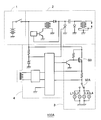
- FIG. 1 is a circuit diagram showing an example of the configuration of the vehicle control apparatus 100 according to the first embodiment.
- FIG. 2 is a circuit diagram showing an example of the configuration of a conventional vehicle control device 100A.
- the vehicle control apparatus 100 (FIG. 1) according to the first embodiment includes a battery B, an ignition switch SWG, a transformer T, a transformer switch element TM, a switch control unit SC, a regulator Y, and a gate.
- Switch element Z N-type MOSFET 10, CPU 20 for control, primary side diode D1, secondary side diode D2, primary side smoothing capacitor C1, secondary side smoothing capacitor C2, and charge / discharge capacitor DC A thyristor A, a spark plug SP, an ignition coil IL, a load switch SWL, and a load La.
- the vehicle control device 100 is mounted on, for example, a motorcycle that is a vehicle.
- the negative electrode of the battery B is connected to the ground.
- the ignition switch SWG has a first node N1 connected to the positive electrode of the battery B and a second node N2.
- the ignition switch SWG is turned on so as to conduct between the first node N1 and the second node N2.
- the ignition switch SWG is turned off to cut off between the first node N1 and the second node N2.
- the ignition switch SWG is operated by a user, for example.
- the transformer T has a primary coil TL1 and a secondary coil TL2.
- the primary coil TL1 has one end connected to the first node N1 of the ignition switch SWG and the other end connected to the ground via the transformer switch element TM.
- the secondary coil TL2 has one end connected to the ground and the other end connected to one end of the charge / discharge capacitor DC.
- the secondary coil TL2 has more turns than the primary coil TL1.
- the transformer T is configured to perform a boost operation in order to supply a voltage for igniting the spark plug SP.
- the transformer switch element TM has one end connected to the other end of the primary coil TL1 and the other end connected to the ground.
- the transformer switch element TM includes an N-type MOSFET for transformer (hereinafter referred to as necessary) having a drain connected to the other end of the primary coil TL1 of the transformer T and a source connected to the ground.
- the code TM is attached accordingly.
- the switch control unit SC controls the transformer switch element TM (outputs a signal to the gate of the transformer N-type MOSFET TM and controls it).
- the switch controller SC is connected between the cathode of the primary diode D1 and the ground, for example, as shown in FIG.
- the switch controller SC controls the transformer N-type MOSFET TM by supplying the gate voltage generated from the voltage at one end of the primary side smoothing capacitor C1 to the gate of the transformer N-type MOSFET TM.
- the primary side diode D1 is connected to the second node N2 of the ignition switch SWG and the transformer T so that the anode is connected to the second node N2 of the ignition switch SWG and the cathode is connected to one end of the primary coil TL1 of the transformer T. Connected to one end of the primary coil TL1.
- the primary side smoothing capacitor C1 has one end connected to the cathode of the primary side diode D1 and the other end connected to the ground.
- one end of the charging / discharging capacitor DC is connected to the other end of the secondary coil TL2 of the transformer T.
- the thyristor A has an anode connected to one end of the charge / discharge capacitor DC and a cathode connected to the ground.
- the thyristor A is controlled by a control signal S3 output from the control CPU 20.
- the ignition coil IL has a primary side connected to the other end of the charge / discharge capacitor DC.
- the spark plug SP is connected between the secondary side of the ignition coil IL and the ground.
- the ignition coil IL has, for example, a primary side ignition coil IL1 and a secondary side ignition coil IL2, as shown in FIG.
- the primary side ignition coil IL1 has one end connected to the other end of the charge / discharge capacitor DC and the other end connected to the ground.
- the secondary side ignition coil IL2 has one end connected to the other end of the primary side ignition coil IL1 and The other end is connected to the spark plug SP.
- the anode of the secondary side diode D2 is connected to the secondary coil TL2 of the transformer T (connected between one end of the secondary coil TL2 and the other end of the secondary coil TL2).
- one end of the secondary side smoothing capacitor C2 is connected to the cathode of the secondary side diode D2, and the other end is connected to the ground.
- the transformer T is boosted to supply a voltage for igniting the spark plug SP, the voltage of the secondary coil TL2 is boosted.
- the voltage of one end (secondary diode D2) of the secondary side smoothing capacitor is set to be higher than the charging voltage of the battery B.
- the regulator Y outputs a step-down voltage obtained by stepping down the voltage of the cathode of the secondary diode D2 (one end of the secondary smoothing capacitor C2).
- one end of the resistance element R is connected to the cathode of the secondary diode D2.
- the N-type MOSFET 10 has a drain connected to the second node N2 of the ignition switch SWG and a gate connected to the other end of the resistance element R. That is, a voltage higher than the charging voltage of the battery B is supplied to the gate of the N-type MOSFET 10 via the resistance element R.
- the load switch SWL has a third node N3 connected to the source of the N-type MOSFET 10 and a fourth node N4.
- the load switch SWL is turned on to conduct between the third node N3 and the fourth node N4.
- the switch element SWL for load interrupts blocks between the 3rd node N3 and the 4th node N4 by turning off.
- the load switch SWL is operated by a user, for example.
- the load La is connected between the fourth node N4 of the load switch SWL and the ground.
- the load La is, for example, a vehicle lamp such as a turn signal of a two-wheeled vehicle.
- the gate switch element Z has one end connected to the gate of the N-type MOSFET 10 and the other end of the resistance element R, and the other end connected to the ground.
- the gate switch element Z is, for example, an NPN bipolar transistor Z having a collector connected to the gate of the N-type MOSFET 10 and an emitter connected to the ground, as shown in FIG.
- control CPU 20 is driven by being supplied with the step-down voltage output from the regulator Y.
- the control CPU 20 controls (turns on / off) the gate switch element Z by a control signal S1 which is a pulse wave.
- the control CPU 20 controls the NPN bipolar transistor Z by a control signal S1, for example, as shown in FIG.
- the control signal S1 to the base of the NPN bipolar transistor of the control CPU 20 is a pulse wave of about 5V (step-down voltage supplied from the regulator Y).
- the pulse wave control signal S2 is supplied to the gate of the N-type MOSFET 10.
- the voltage of the control signal S2 is about 10 and several V higher than the voltage of the control signal S1.
- the voltage at the other end of the resistance element R when the control CPU 20 turns off the NPN-type bipolar transistor Z is based on when the control CPU 20 turns on the NPN-type bipolar transistor Z. It is higher than the supplied voltage (about 5V).
- the voltage supplied to the base of the NPN bipolar transistor Z is generated from the step-down voltage output from the regulator Y.
- control CPU 20 turns on the gate switch element Z, thereby grounding the gate of the N-type MOSFET 10 (that is, making the gate voltage less than the threshold voltage) and turning off the N-type MOSFET 10.
- control CPU 20 turns off the gate switch element Z so that the voltage of the cathode of the secondary diode D2 is applied to the gate of the N-type MOSFET 10 via the resistance element R (that is, the gate).
- the N-type MOSFET 10 is turned on by setting the voltage to a threshold voltage or higher.
- the N-type MOSFET 10 is periodically turned on / off by the control signal S2, so that the load (vehicle lamp) La
- the blinker repeats turning on and off.
- control CPU 20 controls the gate switch element Z so that the vehicle lamp repeatedly turns on and off when the load switch SWL is on, thereby turning on and off the N-type MOSFET 10. And switch.
- a voltage obtained by boosting the battery voltage by the transformer T is supplied to the gate of the N-type MOSFET 10, and the control CPU 20 controls the gate switch element Z, whereby the gate and source of the N-type MOSFET 10 are supplied. The voltage between them is controlled, and the N-type MOSFET 10 is driven in the saturation region.
- an N-type MOSFET that is less expensive than the P-type MOSFET is used as a MOSFET that controls the supply of the battery voltage to the load, and the voltage boosted by the transformer T is supplied to the gate of the N-type MOSFET and the output of the control CPU
- the N-type MOSFET can be driven in the saturation region.
- control CPU 20 outputs a control signal S3 to the gate of the thyristor A, and controls the thyristor A so that the charging / discharging capacitor DC repeats charging / discharging by the control signal S3.
- the spark plug SP repeats ignition.
- the control signal S3 is a pulse wave of about 5V (step-down voltage supplied from the regulator Y).
- the switch controller SC supplies the gate voltage generated from the voltage at one end of the primary side smoothing capacitor C1 to the gate of the transformer N-type MOSFETTM, thereby transducing the transformer.
- the N type MOSFETTM is controlled.
- the transformer T is boosted to supply a voltage for igniting the spark plug SP.
- the regulator Y outputs a step-down voltage obtained by stepping down the voltage (voltage boosted by the transformer T) of the cathode of the secondary side diode D2 (one end of the secondary side smoothing capacitor C2).
- the control CPU 20 is driven by the step-down voltage output from the regulator Y being supplied.
- control CPU 20 turns on the gate switch element Z, thereby grounding the gate of the N-type MOSFET 10 (that is, making the gate voltage less than the threshold voltage) and turning off the N-type MOSFET 10.
- control CPU 20 turns off the gate switch element Z so that the voltage of the cathode of the secondary diode D2 is applied to the gate of the N-type MOSFET 10 via the resistance element R (that is, the gate).
- the N-type MOSFET 10 is turned on by setting the voltage to a threshold voltage or higher.
- the N-type MOSFET 10 is periodically turned on / off by the control signal S2, so that the load (vehicle lamp) La A turn signal of a two-wheeler repeats turning on and off.
- control CPU 20 outputs a control signal S3 to the gate of the thyristor A, and controls the thyristor A by the control signal S3 so that the charging / discharging capacitor DC repeats charging and discharging. As a result, the spark plug SP repeats ignition.
- the vehicle control apparatus 100 includes the battery whose negative electrode is connected to the ground, the first node N1 connected to the positive electrode of the battery, and the second node N2.
- the ignition switch SWG that conducts between the first node N1 and the second node N2 when turned on and shuts off between the first node N1 and the second node N2 when turned off, and one end of the ignition switch SWG.
- a transformer T for boosting operation a transformer switch element TM having one end connected to the other end of the primary coil and the other end connected to the ground, and a transformer switch element T
- a switch control unit SC that controls the voltage, a secondary side diode D2 whose anode is connected to the secondary coil TL2 of the transformer T, a regulator Y that outputs a step-down voltage obtained by stepping down the voltage of the cathode of the secondary side diode D2,
- a resistance element R having one end connected to the cathode of the secondary diode D2, an N-type MOSFET 10 having a drain connected to the second node N2 of the ignition switch SWG and a gate connected to the other end of the resistance element R, and one end Is connected to the gate of the N-type MOSF
- CPU 20 for controlling switch element Z, third node N3 connected to the source of N-type MOSFET 10, A load switch SWL having a node N4, which is turned on to conduct between the third node N3 and the fourth node, and is turned off to cut off between the third node N3 and the fourth node N4; A load La connected between the fourth node N4 of the load switch SWL and the ground.
- a voltage obtained by boosting the battery voltage by the transformer T is supplied to the gate of the N-type MOSFET 10, and the control CPU 20 controls the gate switch element Z, whereby the gate-source between the N-type MOSFET 10 is controlled.
- the voltage is controlled, and the N-type MOSFET 10 is driven in the saturation region.
- control CPU 20 turns on the gate switch element Z to ground the gate of the N-type MOSFET 10 to turn off the N-type MOSFET 10, while turning off the gate switch element Z to turn off the N-type MOSFET 10.
- the N-type MOSFET 10 is turned on so that the voltage of the cathode of the secondary diode D2 is applied to the gate of the second diode D2 via the resistance element R.
- the vehicle control apparatus uses an N-type MOSFET that is less expensive than a P-type MOSFET as a MOSFET that controls the supply of battery voltage to a load, and uses the N-type voltage boosted by a transformer T.
- the N-type MOSFET can be driven in the saturation region.
- the vehicle control apparatus does not require a separate booster circuit for power supply for driving the N-type MOSFET 10.
Landscapes
- Engineering & Computer Science (AREA)
- Mechanical Engineering (AREA)
- Chemical & Material Sciences (AREA)
- Combustion & Propulsion (AREA)
- General Engineering & Computer Science (AREA)
- Ignition Installations For Internal Combustion Engines (AREA)
Abstract
車両用制御装置の制御用CPUは、ゲート用スイッチ素子をオンすることにより、N型MOSFETのゲートを接地してN型MOSFETをオフし、一方、ゲート用スイッチ素子をオフすることにより、N型MOSFETのゲートに抵抗素子を介して二次側ダイオードのカソードの電圧が印加されるようにしてN型MOSFETをオンする。
Description
本発明は、車両用制御装置、および車両用制御装置の制御方法に関する発明である。
車両用制御装置として、例えば、点火装置(CDI:Capacitor Discharge Igniter)が知られている(特開平9-42135参照)。
この特開平9-42135に開示されている車両用制御装置100Aは、直流電源1と、エンジン点火装置2と、車両に装着された方向指示器L1~L4、方向指示器L1~L4の動作を切り替える3点スイッチS2A、直流電源から3点スイッチS2A及び方向指示器L1~L4に給電する給電部よりなる方向指示器駆動部3と、エンジン点火装置2及び方向指示器駆動部3を制御するCPU(Central Processing Unit)部4と、備える(図2参照)。
特に、車両用制御装置100Aの方向指示器駆動部3は、負荷(方向指示器L1~L4)に対するバッテリ電圧の供給を制御するP型MOSFETQ3を備える。
このP型MOSFETQ3は、CPU4の一般的な5V程度の出力により、飽和領域で駆動させることができる。
しかし、一般的に、P型MOSFETは、N型MOSFETよりも高価である。そこで、P型MOSFETよりも安価なN型MOSFETを、負荷に対するバッテリ電圧の供給を制御するMOSFETに適用することが考えられる。
このN型MOSFETを飽和領域で駆動させるためには、ゲート・ソース間の電圧としては、10V程度の電圧が必要になる。
しかし、CPUの一般的な5V程度の出力では、直接N型MOSFETのゲート電圧を制御することにより、N型MOSFETを飽和領域で駆動させることができない。
したがって、CPUの出力電圧を昇圧してN型MOSFETのゲート・ソース間に供給するための電源用の昇圧回路が別途必要になり、製造コストが増加してしまう。
このように、従来の車両用制御装置では、負荷に対するバッテリ電圧の供給を制御するMOSFETとして、N型MOSFETを用いることが困難であった。
本発明は、負荷に対するバッテリ電圧の供給を制御するMOSFETとして、P型MOSFETよりも安価なN型MOSFETを用いるとともに、当該N型MOSFETを飽和領域で駆動させることが可能な車両用制御装置を提供することを目的とする。
本発明の一態様に係る実施例に従った車両用制御装置は、
負極が接地に接続されたバッテリと、
前記バッテリの正極に接続された第1ノードと、第2ノードとを有し、オンすることにより前記第1ノードと前記第2ノードとの間を導通し、オフすることにより前記第1ノードと前記第2ノードとの間を遮断するイグニッションスイッチと、
一端が前記イグニッションスイッチの前記第1ノードに接続された一次コイルと、一端が前記接地に接続され且つ前記一次コイルよりも巻数が多い二次コイルと、を有し、スパークプラグを点火する電圧を供給するために昇圧動作するトランスと、
一端が前記一次コイルの他端に接続され、他端が前記接地に接続されたトランス用スイッチ素子と、
前記トランス用スイッチ素子を制御するスイッチ制御部と、
アノードが前記トランスの前記二次コイルに接続された二次側ダイオードと、
前記二次側ダイオードのカソードの電圧を降圧した降圧電圧を出力するレギュレータと、
一端が前記二次側ダイオードのカソードに接続された抵抗素子と、
ドレインが前記イグニッションスイッチの前記第2ノードに接続され、ゲートが前記抵抗素子の他端に接続されたN型MOSFETと、
一端が前記N型MOSFETのゲート及び前記抵抗素子の他端に接続され、他端が前記接地に接続されたゲート用スイッチ素子と、
前記レギュレータが出力した前記降圧電圧が供給されることにより駆動し、前記ゲート用スイッチ素子を制御する制御用CPUと、
前記N型MOSFETのソースに接続された第3ノードと、第4ノードとを有し、オンすることにより前記第3ノードと前記第4ノードとの間を導通し、オフすることにより前記第3ノードと前記第4ノードとの間を遮断する負荷用スイッチと、
前記負荷用スイッチの前記第4ノードと前記接地との間に接続された負荷と、を備える
ことを特徴とする。
負極が接地に接続されたバッテリと、
前記バッテリの正極に接続された第1ノードと、第2ノードとを有し、オンすることにより前記第1ノードと前記第2ノードとの間を導通し、オフすることにより前記第1ノードと前記第2ノードとの間を遮断するイグニッションスイッチと、
一端が前記イグニッションスイッチの前記第1ノードに接続された一次コイルと、一端が前記接地に接続され且つ前記一次コイルよりも巻数が多い二次コイルと、を有し、スパークプラグを点火する電圧を供給するために昇圧動作するトランスと、
一端が前記一次コイルの他端に接続され、他端が前記接地に接続されたトランス用スイッチ素子と、
前記トランス用スイッチ素子を制御するスイッチ制御部と、
アノードが前記トランスの前記二次コイルに接続された二次側ダイオードと、
前記二次側ダイオードのカソードの電圧を降圧した降圧電圧を出力するレギュレータと、
一端が前記二次側ダイオードのカソードに接続された抵抗素子と、
ドレインが前記イグニッションスイッチの前記第2ノードに接続され、ゲートが前記抵抗素子の他端に接続されたN型MOSFETと、
一端が前記N型MOSFETのゲート及び前記抵抗素子の他端に接続され、他端が前記接地に接続されたゲート用スイッチ素子と、
前記レギュレータが出力した前記降圧電圧が供給されることにより駆動し、前記ゲート用スイッチ素子を制御する制御用CPUと、
前記N型MOSFETのソースに接続された第3ノードと、第4ノードとを有し、オンすることにより前記第3ノードと前記第4ノードとの間を導通し、オフすることにより前記第3ノードと前記第4ノードとの間を遮断する負荷用スイッチと、
前記負荷用スイッチの前記第4ノードと前記接地との間に接続された負荷と、を備える
ことを特徴とする。
前記車両用制御装置において、
前記制御用CPUは、
前記ゲート用スイッチ素子をオンすることにより、前記N型MOSFETのゲートを接地して前記N型MOSFETをオフし、
一方、前記ゲート用スイッチ素子をオフすることにより、前記N型MOSFETのゲートに前記抵抗素子を介して前記二次側ダイオードのカソードの電圧が印加されるようにして前記N型MOSFETをオンする
ことを特徴とする。
前記制御用CPUは、
前記ゲート用スイッチ素子をオンすることにより、前記N型MOSFETのゲートを接地して前記N型MOSFETをオフし、
一方、前記ゲート用スイッチ素子をオフすることにより、前記N型MOSFETのゲートに前記抵抗素子を介して前記二次側ダイオードのカソードの電圧が印加されるようにして前記N型MOSFETをオンする
ことを特徴とする。
前記車両用制御装置において、
前記ゲート用スイッチ素子は、
コレクタが前記N型MOSFETのゲートに接続され、エミッタが前記接地に接続されたNPN型バイポーラトランジスタであり、
前記制御用CPUは、
前記NPN型バイポーラトランジスタを制御することを特徴とする。
前記ゲート用スイッチ素子は、
コレクタが前記N型MOSFETのゲートに接続され、エミッタが前記接地に接続されたNPN型バイポーラトランジスタであり、
前記制御用CPUは、
前記NPN型バイポーラトランジスタを制御することを特徴とする。
前記車両用制御装置において、
前記車両用制御装置は、
一端が前記トランスの前記二次コイルの他端に接続された充放電用コンデンサと、
アノードが前記充放電用コンデンサの前記一端に接続され、カソードが前記接地に接続されたサイリスタと、
一次側が前記充放電用コンデンサの他端に接続されたイグニッションコイルと、前記イグニッションコイルの二次側と前記接地との間に接続されたスパークプラグと、をさらに備え、
前記制御用CPUは、
前記充放電用コンデンサが充放電を繰り返すように、前記サイリスタを制御することを特徴とする。
前記車両用制御装置は、
一端が前記トランスの前記二次コイルの他端に接続された充放電用コンデンサと、
アノードが前記充放電用コンデンサの前記一端に接続され、カソードが前記接地に接続されたサイリスタと、
一次側が前記充放電用コンデンサの他端に接続されたイグニッションコイルと、前記イグニッションコイルの二次側と前記接地との間に接続されたスパークプラグと、をさらに備え、
前記制御用CPUは、
前記充放電用コンデンサが充放電を繰り返すように、前記サイリスタを制御することを特徴とする。
前記車両用制御装置において、
前記制御用CPUが前記NPN型バイポーラトランジスタをオフさせているときの前記抵抗素子の他端の電圧は、前記制御用CPUが前記NPN型バイポーラトランジスタをオンさせるときにベースに供給する電圧よりも、高くなっており、
前記ベースに供給される電圧は、前記レギュレータが出力した前記降圧電圧から生成される
ことを特徴とする。
前記制御用CPUが前記NPN型バイポーラトランジスタをオフさせているときの前記抵抗素子の他端の電圧は、前記制御用CPUが前記NPN型バイポーラトランジスタをオンさせるときにベースに供給する電圧よりも、高くなっており、
前記ベースに供給される電圧は、前記レギュレータが出力した前記降圧電圧から生成される
ことを特徴とする。
前記車両用制御装置において、
前記負荷は、車両用ランプであり、
前記制御用CPUは、前記負荷用スイッチがオンしている場合に前記車両用ランプが点灯と消灯とを繰り返すように、前記ゲート用スイッチ素子を制御することにより前記N型MOSFETのオンとオフとを切り替える
ことを特徴とする。
前記負荷は、車両用ランプであり、
前記制御用CPUは、前記負荷用スイッチがオンしている場合に前記車両用ランプが点灯と消灯とを繰り返すように、前記ゲート用スイッチ素子を制御することにより前記N型MOSFETのオンとオフとを切り替える
ことを特徴とする。
前記車両用制御装置において、
一端が前記二次側ダイオードのカソードに接続され、他端が前記接地に接続された二次側平滑化コンデンサをさらに備える
ことを特徴とする。
一端が前記二次側ダイオードのカソードに接続され、他端が前記接地に接続された二次側平滑化コンデンサをさらに備える
ことを特徴とする。
前記車両用制御装置において、
アノードが前記イグニッションスイッチの前記第2ノードに接続され且つカソードが前記トランスの一次コイルの一端に接続されるように、前記イグニッションスイッチの前記第2ノードと前記トランスの一次コイルの一端との間に接続された一次側ダイオードをさらに備えることを特徴とする。
アノードが前記イグニッションスイッチの前記第2ノードに接続され且つカソードが前記トランスの一次コイルの一端に接続されるように、前記イグニッションスイッチの前記第2ノードと前記トランスの一次コイルの一端との間に接続された一次側ダイオードをさらに備えることを特徴とする。
前記車両用制御装置において、
前記一次側ダイオードのカソードに一端が接続され、他端が前記接地に接続された一次側平滑化コンデンサをさらに備えることを特徴とする。
前記一次側ダイオードのカソードに一端が接続され、他端が前記接地に接続された一次側平滑化コンデンサをさらに備えることを特徴とする。
前記車両用制御装置において、
前記二次側平滑化コンデンサの前記一端の電圧は、前記バッテリの充電電圧よりも、高いことを特徴とする。
前記二次側平滑化コンデンサの前記一端の電圧は、前記バッテリの充電電圧よりも、高いことを特徴とする。
前記車両用制御装置において、
前記トランス用スイッチ素子は、ドレインが前記トランスの前記一次コイルの前記他端に接続され、ソースが前記接地に接続されたトランス用N型MOSFETであることを特徴とする。
前記トランス用スイッチ素子は、ドレインが前記トランスの前記一次コイルの前記他端に接続され、ソースが前記接地に接続されたトランス用N型MOSFETであることを特徴とする。
前記車両用制御装置において、
前記スイッチ制御部は、前記一次側平滑化コンデンサの前記一端の電圧から生成したゲート電圧を、前記トランス用N型MOSFETのゲートに供給することにより、前記トランス用N型MOSFETを制御する
ことを特徴とする。
前記スイッチ制御部は、前記一次側平滑化コンデンサの前記一端の電圧から生成したゲート電圧を、前記トランス用N型MOSFETのゲートに供給することにより、前記トランス用N型MOSFETを制御する
ことを特徴とする。
前記車両用制御装置において、
前記イグニッションコイルは、
一端が前記充放電用コンデンサの前記他端に接続され、且つ他端が前記接地に接続された一次側イグニッションコイルと、
一端が前記一次側イグニッションコイルの前記他端及び前記接地に接続され、且つ他端が前記スパークプラグに接続された二次側イグニッションコイルと、を有する
ことを特徴とする。
前記イグニッションコイルは、
一端が前記充放電用コンデンサの前記他端に接続され、且つ他端が前記接地に接続された一次側イグニッションコイルと、
一端が前記一次側イグニッションコイルの前記他端及び前記接地に接続され、且つ他端が前記スパークプラグに接続された二次側イグニッションコイルと、を有する
ことを特徴とする。
前記車両用制御装置において、
前記車両用制御装置は、車両である二輪車に積載され、
前記車両用ランプは、前記二輪車のウインカーであり、
前記イグニッションスイッチ及び負荷用スイッチは、ユーザにより操作される
ことを特徴とする。
前記車両用制御装置は、車両である二輪車に積載され、
前記車両用ランプは、前記二輪車のウインカーであり、
前記イグニッションスイッチ及び負荷用スイッチは、ユーザにより操作される
ことを特徴とする。
本発明の一態様に係る実施例に従った車両用制御装置の制御方法は、
負極が接地に接続されたバッテリと、前記バッテリの正極に接続された第1ノードと、第2ノードとを有し、オンすることにより前記第1ノードと前記第2ノードとの間を導通し、オフすることにより前記第1ノードと前記第2ノードとの間を遮断するイグニッションスイッチと、一端が前記イグニッションスイッチの前記第1ノードに接続された一次コイルと、一端が前記接地に接続され且つ前記一次コイルよりも巻数が多い二次コイルと、を有し、スパークプラグを点火する電圧を供給するために昇圧動作するトランスと、一端が前記一次コイルの他端に接続され、他端が前記接地に接続されたトランス用スイッチ素子と、前記トランス用スイッチ素子を制御するスイッチ制御部と、アノードが前記トランスの前記二次コイルに接続された二次側ダイオードと、前記二次側ダイオードのカソードの電圧を降圧した降圧電圧を出力するレギュレータと、一端が前記二次側ダイオードのカソードに接続された抵抗素子と、ドレインが前記イグニッションスイッチの前記第2ノードに接続され、ゲートが前記抵抗素子の他端に接続されたN型MOSFETと、一端が前記N型MOSFETのゲート及び前記抵抗素子の他端に接続され、他端が前記接地に接続されたゲート用スイッチ素子と、前記レギュレータが出力した前記降圧電圧が供給されることにより駆動し、前記ゲート用スイッチ素子を制御する制御用CPUと、前記N型MOSFETのソースに接続された第3ノードと、第4ノードとを有し、オンすることにより前記第3ノードと前記第4ノードとの間を導通し、オフすることにより前記第3ノードと前記第4ノードとの間を遮断する負荷用スイッチと、前記負荷用スイッチの前記第4ノードと前記接地との間に接続された負荷と、を備えた車両用制御装置の制御方法であって、
前記制御用CPUが前記ゲート用スイッチ素子をオンすることにより、前記N型MOSFETのゲートを接地して前記N型MOSFETをオフし、
一方、前記制御用CPUが前記ゲート用スイッチ素子をオフすることにより、前記N型MOSFETのゲートに前記抵抗素子を介して前記二次側ダイオードのカソードの電圧が印加されるようにして前記N型MOSFETをオンする
ことを特徴とする。
負極が接地に接続されたバッテリと、前記バッテリの正極に接続された第1ノードと、第2ノードとを有し、オンすることにより前記第1ノードと前記第2ノードとの間を導通し、オフすることにより前記第1ノードと前記第2ノードとの間を遮断するイグニッションスイッチと、一端が前記イグニッションスイッチの前記第1ノードに接続された一次コイルと、一端が前記接地に接続され且つ前記一次コイルよりも巻数が多い二次コイルと、を有し、スパークプラグを点火する電圧を供給するために昇圧動作するトランスと、一端が前記一次コイルの他端に接続され、他端が前記接地に接続されたトランス用スイッチ素子と、前記トランス用スイッチ素子を制御するスイッチ制御部と、アノードが前記トランスの前記二次コイルに接続された二次側ダイオードと、前記二次側ダイオードのカソードの電圧を降圧した降圧電圧を出力するレギュレータと、一端が前記二次側ダイオードのカソードに接続された抵抗素子と、ドレインが前記イグニッションスイッチの前記第2ノードに接続され、ゲートが前記抵抗素子の他端に接続されたN型MOSFETと、一端が前記N型MOSFETのゲート及び前記抵抗素子の他端に接続され、他端が前記接地に接続されたゲート用スイッチ素子と、前記レギュレータが出力した前記降圧電圧が供給されることにより駆動し、前記ゲート用スイッチ素子を制御する制御用CPUと、前記N型MOSFETのソースに接続された第3ノードと、第4ノードとを有し、オンすることにより前記第3ノードと前記第4ノードとの間を導通し、オフすることにより前記第3ノードと前記第4ノードとの間を遮断する負荷用スイッチと、前記負荷用スイッチの前記第4ノードと前記接地との間に接続された負荷と、を備えた車両用制御装置の制御方法であって、
前記制御用CPUが前記ゲート用スイッチ素子をオンすることにより、前記N型MOSFETのゲートを接地して前記N型MOSFETをオフし、
一方、前記制御用CPUが前記ゲート用スイッチ素子をオフすることにより、前記N型MOSFETのゲートに前記抵抗素子を介して前記二次側ダイオードのカソードの電圧が印加されるようにして前記N型MOSFETをオンする
ことを特徴とする。
本発明の一態様に係る車両用制御装置は、負極が接地に接続されたバッテリと、バッテリの正極に接続された第1ノードと、第2ノードとを有し、オンすることにより第1ノードと第2ノードとの間を導通し、オフすることにより第1ノードと第2ノードとの間を遮断するイグニッションスイッチと、一端がイグニッションスイッチの第1ノードに接続された一次コイルと、一端が接地に接続され且つ一次コイルよりも巻数が多い二次コイルと、を有し、スパークプラグを点火する電圧を供給するために昇圧動作するトランスと、一端が一次コイルの他端に接続され、他端が接地に接続されたトランス用スイッチ素子と、トランス用スイッチ素子を制御するスイッチ制御部と、アノードがトランスの二次コイルに接続された二次側ダイオードと、二次側ダイオードのカソードの電圧を降圧した降圧電圧を出力するレギュレータと、一端が二次側ダイオードのカソードに接続された抵抗素子と、ドレインがイグニッションスイッチの第2ノードに接続され、ゲートが抵抗素子の他端に接続されたN型MOSFETと、一端がN型MOSFETのゲート及び抵抗素子の他端に接続され、他端が接地に接続されたゲート用スイッチ素子と、レギュレータが出力した降圧電圧が供給されることにより駆動し、ゲート用スイッチ素子を制御する制御用CPUと、N型MOSFETのソースに接続された第3ノードと、第4ノードとを有し、オンすることにより第3ノードと4ノードとの間を導通し、オフすることにより第3ノードと第4ノードとの間を遮断する負荷用スイッチと、負荷用スイッチの第4ノードと接地との間に接続された負荷と、を備える。
これにより、トランスによりバッテリ電圧を昇圧した電圧がN型MOSFETのゲートへ供給されるようになり、制御用CPUがゲート用スイッチ素子を制御することで、N型MOSFETのゲート・ソース間の電圧が制御され、N型MOSFETが飽和領域で駆動される。
例えば、制御用CPUは、ゲート用スイッチ素子をオンすることにより、N型MOSFETのゲートを接地してN型MOSFETをオフし、一方、ゲート用スイッチ素子をオフすることにより、N型MOSFETのゲートに抵抗素子を介して二次側ダイオードのカソードの電圧が印加されるようにしてN型MOSFETをオンする。
このように、本発明に係る車両用制御装置は、負荷に対するバッテリ電圧の供給を制御するMOSFETとして、P型MOSFETよりも安価なN型MOSFETを用いるとともに、トランスで昇圧した電圧を当該N型MOSFETのゲートに供給し且つ制御用CPUの出力でゲート・ソース間の電圧を制御することにより、当該N型MOSFETを飽和領域で駆動させることができる。
特に、本発明に係る車両用制御装置は、N型MOSFETを駆動するための電源用の昇圧回路を別途追加する必要が無い。
以下、本発明に係る実施形態について図面に基づいて説明する。
第1の実施形態に係る車両用制御装置100(図1)は、バッテリBと、イグニッションスイッチSWGと、トランスTと、トランス用スイッチ素子TMと、スイッチ制御部SCと、レギュレータYと、ゲート用スイッチ素子Zと、N型MOSFET10と、制御用CPU20と、一次側ダイオードD1と、二次側ダイオードD2と、一次側平滑化コンデンサC1と、二次側平滑化コンデンサC2と、充放電用コンデンサDCと、サイリスタAと、スパークプラグSPと、イグニッションコイルILと、負荷用スイッチSWLと、負荷Laと、を備える。
この車両用制御装置100は、例えば、車両である二輪車に積載される。
ここで、バッテリBは、負極が接地に接続されている。
また、イグニッションスイッチSWGは、バッテリBの正極に接続された第1ノードN1と、第2ノードN2とを有する。このイグニッションスイッチSWGは、オンすることにより第1ノードN1と第2ノードN2との間を導通するようになっている。一方、イグニッションスイッチSWGは、オフすることにより第1ノードN1と第2ノードN2との間を遮断するようになっている。
このイグニッションスイッチSWGは、例えば、ユーザにより操作されるようになっている。
トランスTは、一次コイルTL1と、二次コイルTL2と、を有する。
一次コイルTL1は、一端がイグニッションスイッチSWGの第1ノードN1に接続され、他端が、トランス用スイッチ素子TMを介して、接地に接続されている。
二次コイルTL2は、一端が接地に接続され、他端が充放電用コンデンサDCの一端に接続されている。この二次コイルTL2は、一次コイルTL1よりも巻数が多い。
このトランスTは、スパークプラグSPを点火する電圧を供給するために昇圧動作するようになっている。
トランス用スイッチ素子TMは、一端が一次コイルTL1の他端に接続され、他端が接地に接続されている。
このトランス用スイッチ素子TMは、例えば、図1に示すように、ドレインがトランスTの一次コイルTL1の他端に接続され、ソースが接地に接続されたトランス用N型MOSFET(以下では、必要に応じて符号TMを付する)である。
スイッチ制御部SCは、トランス用スイッチ素子TMを制御する(トランス用N型MOSFETTMのゲートに信号を出力して制御する)ようになっている。
このスイッチ制御部SCは、例えば、図1に示すように、一次側ダイオードD1のカソードと接地との間に接続され、バッテリBから電力が供給されるようになっている。この場合、スイッチ制御部SCは、一次側平滑化コンデンサC1の一端の電圧から生成したゲート電圧を、トランス用N型MOSFETTMのゲートに供給することにより、トランス用N型MOSFETTMを制御する。
また、一次側ダイオードD1は、アノードがイグニッションスイッチSWGの第2ノードN2に接続され且つカソードがトランスTの一次コイルTL1の一端に接続されるように、イグニッションスイッチSWGの第2ノードN2とトランスTの一次コイルTL1の一端との間に接続されている。
また、一次側平滑化コンデンサC1は、一次側ダイオードD1のカソードに一端が接続され、他端が接地に接続されている。
また、充放電用コンデンサDCは、一端がトランスTの二次コイルTL2の他端に接続されている。
サイリスタAは、アノードが充放電用コンデンサDCの一端に接続され、カソードが接地に接続されている。このサイリスタAは、制御用CPU20が出力する制御信号S3により、制御される。
また、イグニッションコイルILは、一次側が充放電用コンデンサDCの他端に接続されている。
スパークプラグSPは、イグニッションコイルILの二次側と接地との間に接続されている。
ここで、イグニッションコイルILは、例えば、図1に示すように、一次側イグニッションコイルIL1と、二次側イグニッションコイルIL2と、を有する。
一次側イグニッションコイルIL1は、一端が充放電用コンデンサDCの他端に接続され、且つ他端が接地に接続されている
二次側イグニッションコイルIL2は、一端が一次側イグニッションコイルIL1の他端及び接地に接続され、且つ他端がスパークプラグSPに接続されている。
二次側イグニッションコイルIL2は、一端が一次側イグニッションコイルIL1の他端及び接地に接続され、且つ他端がスパークプラグSPに接続されている。
また、二次側ダイオードD2は、アノードがトランスTの二次コイルTL2に接続(二次コイルTL2の一端と二次コイルTL2の他端との間に接続)されている。
また、二次側平滑化コンデンサC2は、一端が二次側ダイオードD2のカソードに接続され、他端が接地に接続されている。
ここで、既述のように、トランスTは、スパークプラグSPを点火する電圧を供給するために昇圧動作するようになっているため、二次コイルTL2の電圧は昇圧されている。これにより、二次側平滑化コンデンサの一端(二次側ダイオードD2)の電圧は、バッテリBの充電電圧よりも、高くなるように設定されている。
また、レギュレータYは、二次側ダイオードD2のカソード(二次側平滑化コンデンサC2の一端)の電圧を降圧した降圧電圧を出力するようになっている。
また、抵抗素子Rは、一端が二次側ダイオードD2のカソードに接続されている。
N型MOSFET10は、ドレインがイグニッションスイッチSWGの第2ノードN2に接続され、ゲートが抵抗素子Rの他端に接続されている。すなわち、N型MOSFET10のゲートは、抵抗素子Rを介してバッテリBの充電電圧よりも高い電圧が供給されるようになっている。
また、負荷用スイッチSWLは、N型MOSFET10のソースに接続された第3ノードN3と、第4ノードN4とを有する。
この負荷用スイッチSWLは、オンすることにより第3ノードN3と第4ノードN4との間を導通するようになっている。一方、負荷用スイッチ素子SWLは、オフすることにより第3ノードN3と第4ノードN4との間を遮断するようになっている。
この負荷用スイッチSWLは、例えば、ユーザにより操作されるようになっている。
また、負荷Laは、負荷用スイッチSWLの第4ノードN4と接地との間に接続されている。この負荷Laは、例えば、二輪車のウインカー等の車両用ランプである。
また、ゲート用スイッチ素子Zは、一端がN型MOSFET10のゲート及び抵抗素子Rの他端に接続され、他端が接地に接続されている。
このゲート用スイッチ素子Zは、例えば、図1に示すように、コレクタがN型MOSFET10のゲートに接続され、エミッタが接地に接続されたNPN型バイポーラトランジスタZである。
このゲート用スイッチ素子Zがオンすることにより、N型MOSFET10のゲートが接地され、N型MOSFET10がオフする。
一方、ゲート用スイッチ素子Zがオフすることにより、N型MOSFET10のゲートに抵抗素子Rを介して電圧が供給され、N型MOSFET10がオンする。
また、制御用CPU20は、レギュレータYが出力した降圧電圧が供給されることにより駆動する。そして、制御用CPU20は、パルス波である制御信号S1により、ゲート用スイッチ素子Zを制御(オン/オフ)するようになっている。
制御用CPU20は、例えば、図1に示すように、制御信号S1により、NPN型バイポーラトランジスタZを制御する。このとき、制御用CPU20のNPN型バイポーラトランジスタのベースへの制御信号S1は、5V程度(レギュレータYから供給された降圧電圧)のパルス波である。
このように、ゲート用スイッチ素子Zをオン/オフすることにより、N型MOSFET10のゲートにパルス波の制御信号S2が供給されることとなる。この制御信号S2の電圧は、制御信号S1の電圧よりも高い、10数V程度になる。
すなわち、制御用CPU20がNPN型バイポーラトランジスタZをオフさせているときの抵抗素子Rの他端の電圧(10数V程度)は、制御用CPU20がNPN型バイポーラトランジスタZをオンさせるときにベースに供給する電圧(5V程度)よりも、高くなっている。そして、NPN型バイポーラトランジスタZのベースに供給される電圧は、レギュレータYが出力した降圧電圧から生成されている。
ここで、例えば、制御用CPU20は、ゲート用スイッチ素子Zをオンすることにより、N型MOSFET10のゲートを接地して(すなわち、ゲート電圧を閾値電圧未満にして)、N型MOSFET10をオフする。
一方、制御用CPU20は、ゲート用スイッチ素子Zをオフすることにより、N型MOSFET10のゲートに抵抗素子Rを介して二次側ダイオードD2のカソードの電圧が印加されるようにして(すなわち、ゲート電圧を閾値電圧以上にして)、N型MOSFET10をオンする。
なお、イグニッションスイッチSWG及び負荷用スイッチSWLがオンしている場合、このN型MOSFET10が周期的に制御信号S2によりオン/オフに制御されることにより、負荷(車両用ランプ)Laである二輪車のウインカーが点灯と消灯とを繰り返すこととなる。
このように、制御用CPU20は、負荷用スイッチSWLがオンしている場合に車両用ランプが点灯と消灯とを繰り返すように、ゲート用スイッチ素子Zを制御することによりN型MOSFET10のオンとオフとを切り替える。
上述のように、トランスTによりバッテリ電圧を昇圧した電圧がN型MOSFET10のゲートへ供給されるようになり、制御用CPU20がゲート用スイッチ素子Zを制御することで、N型MOSFET10のゲート・ソース間の電圧が制御され、N型MOSFET10が飽和領域で駆動される。
すなわち、負荷に対するバッテリ電圧の供給を制御するMOSFETとして、P型MOSFETよりも安価なN型MOSFETを用いるとともに、トランスTで昇圧した電圧を当該N型MOSFETのゲートに供給し且つ制御用CPUの出力でゲート・ソース間の電圧を制御することにより、当該N型MOSFETを飽和領域で駆動させることができる。
また、制御用CPU20は、制御信号S3をサイリスタAのゲートに出力し、この制御信号S3により、充放電用コンデンサDCが充放電を繰り返すように、サイリスタAを制御する。これにより、スパークプラグSPが点火を繰り返すこととなる。
なお、制御信号S3は、5V程度(レギュレータYから供給された降圧電圧)のパルス波である。
次に、以上のような構成を有する車両用制御装置100の動作の一例について説明する。
例えば、ユーザによりイグニッションスイッチSWGがオンされると、スイッチ制御部SCは、一次側平滑化コンデンサC1の一端の電圧から生成したゲート電圧を、トランス用N型MOSFETTMのゲートに供給することにより、トランス用N型MOSFETTMを制御する。
これにより、トランスTは、スパークプラグSPを点火する電圧を供給するために昇圧動作する。
そして、レギュレータYは、二次側ダイオードD2のカソード(二次側平滑化コンデンサC2の一端)の電圧(トランスTが昇圧した電圧)を降圧した降圧電圧を出力する。
そして、制御用CPU20は、レギュレータYが出力した降圧電圧が供給されることにより駆動する。
そして、例えば、制御用CPU20は、ゲート用スイッチ素子Zをオンすることにより、N型MOSFET10のゲートを接地して(すなわち、ゲート電圧を閾値電圧未満にして)、N型MOSFET10をオフする。
一方、制御用CPU20は、ゲート用スイッチ素子Zをオフすることにより、N型MOSFET10のゲートに抵抗素子Rを介して二次側ダイオードD2のカソードの電圧が印加されるようにして(すなわち、ゲート電圧を閾値電圧以上にして)、N型MOSFET10をオンする。
なお、ユーザの操作によりイグニッションスイッチSWG及び負荷用スイッチSWLがオンしている場合、N型MOSFET10が周期的に制御信号S2によりオン/オフに制御されることにより、負荷(車両用ランプ)Laである二輪車のウインカーが点灯と消灯とを繰り返すこととなる。
一方、制御用CPU20は、制御信号S3をサイリスタAのゲートに出力し、この制御信号S3により、充放電用コンデンサDCが充放電を繰り返すように、サイリスタAを制御する。これにより、スパークプラグSPが点火を繰り返すこととなる。
以上のように、本発明の一態様に係る車両用制御装置100は、負極が接地に接続されたバッテリと、バッテリの正極に接続された第1ノードN1と、第2ノードN2とを有し、オンすることにより第1ノードN1と第2ノードN2との間を導通し、オフすることにより第1ノードN1と第2ノードN2との間を遮断するイグニッションスイッチSWGと、一端がイグニッションスイッチSWGの第1ノードN1に接続された一次コイルTL1と、一端が接地に接続され且つ一次コイルよりも巻数が多い二次コイルTL2と、を有し、スパークプラグSPを点火する電圧を供給するために昇圧動作するトランスTと、一端が一次コイルの他端に接続され、他端が接地に接続されたトランス用スイッチ素子TMと、トランス用スイッチ素子TMを制御するスイッチ制御部SCと、アノードがトランスTの二次コイルTL2に接続された二次側ダイオードD2と、二次側ダイオードD2のカソードの電圧を降圧した降圧電圧を出力するレギュレータYと、一端が二次側ダイオードD2のカソードに接続された抵抗素子Rと、ドレインがイグニッションスイッチSWGの第2ノードN2に接続され、ゲートが抵抗素子Rの他端に接続されたN型MOSFET10と、一端がN型MOSFET10のゲート及び抵抗素子Rの他端に接続され、他端が接地に接続されたゲート用スイッチ素子Zと、レギュレータYが出力した降圧電圧が供給されることにより駆動し、ゲート用スイッチ素子Zを制御する制御用CPU20と、N型MOSFET10のソースに接続された第3ノードN3と、第4ノードN4とを有し、オンすることにより第3ノードN3と4ノードとの間を導通し、オフすることにより第3ノードN3と第4ノードN4との間を遮断する負荷用スイッチSWLと、負荷用スイッチSWLの第4ノードN4と接地との間に接続された負荷Laと、を備える。
これにより、トランスTによりバッテリ電圧を昇圧した電圧がN型MOSFET10のゲートへ供給されるようになり、制御用CPU20がゲート用スイッチ素子Zを制御することで、N型MOSFET10のゲート・ソース間の電圧が制御され、N型MOSFET10が飽和領域で駆動される。
例えば、制御用CPU20は、ゲート用スイッチ素子Zをオンすることにより、N型MOSFET10のゲートを接地してN型MOSFET10をオフし、一方、ゲート用スイッチ素子Zをオフすることにより、N型MOSFET10のゲートに抵抗素子Rを介して二次側ダイオードD2のカソードの電圧が印加されるようにしてN型MOSFET10をオンする。
このように、本発明に係る車両用制御装置は、負荷に対するバッテリ電圧の供給を制御するMOSFETとして、P型MOSFETよりも安価なN型MOSFETを用いるとともに、トランスTで昇圧した電圧を当該N型MOSFETのゲートに供給し且つ制御用CPUの出力でゲート・ソース間の電圧を制御することにより、当該N型MOSFETを飽和領域で駆動させることができる。
特に、本発明に係る車両用制御装置は、N型MOSFET10を駆動するための電源用の昇圧回路を別途追加する必要が無い。
本発明のいくつかの実施形態を説明したが、これらの実施形態は、例として提示したものであり、発明の範囲を限定することは意図していない。これら実施形態は、その他の様々な形態で実施されることが可能であり、発明の要旨を逸脱しない範囲で、種々の省略、置き換え、変更を行うことができる。これら実施形態やその変形は、発明の範囲や要旨に含まれると同様に、特許請求の範囲に記載された発明とその均等の範囲に含まれるものである。
Claims (15)
- 負極が接地に接続されたバッテリと、
前記バッテリの正極に接続された第1ノードと、第2ノードとを有し、オンすることにより前記第1ノードと前記第2ノードとの間を導通し、オフすることにより前記第1ノードと前記第2ノードとの間を遮断するイグニッションスイッチと、
一端が前記イグニッションスイッチの前記第1ノードに接続された一次コイルと、一端が前記接地に接続され且つ前記一次コイルよりも巻数が多い二次コイルと、を有し、スパークプラグを点火する電圧を供給するために昇圧動作するトランスと、
一端が前記一次コイルの他端に接続され、他端が前記接地に接続されたトランス用スイッチ素子と、
前記トランス用スイッチ素子を制御するスイッチ制御部と、
アノードが前記トランスの前記二次コイルに接続された二次側ダイオードと、
前記二次側ダイオードのカソードの電圧を降圧した降圧電圧を出力するレギュレータと、
一端が前記二次側ダイオードのカソードに接続された抵抗素子と、
ドレインが前記イグニッションスイッチの前記第2ノードに接続され、ゲートが前記抵抗素子の他端に接続されたN型MOSFETと、
一端が前記N型MOSFETのゲート及び前記抵抗素子の他端に接続され、他端が前記接地に接続されたゲート用スイッチ素子と、
前記レギュレータが出力した前記降圧電圧が供給されることにより駆動し、前記ゲート用スイッチ素子を制御する制御用CPUと、
前記N型MOSFETのソースに接続された第3ノードと、第4ノードとを有し、オンすることにより前記第3ノードと前記第4ノードとの間を導通し、オフすることにより前記第3ノードと前記第4ノードとの間を遮断する負荷用スイッチと、
前記負荷用スイッチの前記第4ノードと前記接地との間に接続された負荷と、を備える
ことを特徴とする車両用制御装置。 - 前記制御用CPUは、
前記ゲート用スイッチ素子をオンすることにより、前記N型MOSFETのゲートを接地して前記N型MOSFETをオフし、
一方、前記ゲート用スイッチ素子をオフすることにより、前記N型MOSFETのゲートに前記抵抗素子を介して前記二次側ダイオードのカソードの電圧が印加されるようにして前記N型MOSFETをオンする
ことを特徴とする請求項1に記載の車両用制御装置。 - 前記ゲート用スイッチ素子は、
コレクタが前記N型MOSFETのゲートに接続され、エミッタが前記接地に接続されたNPN型バイポーラトランジスタであり、
前記制御用CPUは、
前記NPN型バイポーラトランジスタを制御することを特徴とする請求項2に記載の車両用制御装置。 - 前記車両用制御装置は、
一端が前記トランスの前記二次コイルの他端に接続された充放電用コンデンサと、
アノードが前記充放電用コンデンサの前記一端に接続され、カソードが前記接地に接続されたサイリスタと、
一次側が前記充放電用コンデンサの他端に接続されたイグニッションコイルと、前記イグニッションコイルの二次側と前記接地との間に接続されたスパークプラグと、をさらに備え、
前記制御用CPUは、
前記充放電用コンデンサが充放電を繰り返すように、前記サイリスタを制御することを特徴とする請求項3に記載の車両用制御装置。 - 前記制御用CPUが前記NPN型バイポーラトランジスタをオフさせているときの前記抵抗素子の他端の電圧は、前記制御用CPUが前記NPN型バイポーラトランジスタをオンさせるときにベースに供給する電圧よりも、高くなっており、
前記ベースに供給される電圧は、前記レギュレータが出力した前記降圧電圧から生成される
ことを特徴とする請求項4に記載の車両用制御装置。 - 前記負荷は、車両用ランプであり、
前記制御用CPUは、前記負荷用スイッチがオンしている場合に前記車両用ランプが点灯と消灯とを繰り返すように、前記ゲート用スイッチ素子を制御することにより前記N型MOSFETのオンとオフとを切り替える
ことを特徴とする請求項4に記載の車両用制御装置。 - 一端が前記二次側ダイオードのカソードに接続され、他端が前記接地に接続された二次側平滑化コンデンサをさらに備える
ことを特徴とする請求項5に記載の車両用制御装置。 - アノードが前記イグニッションスイッチの前記第2ノードに接続され且つカソードが前記トランスの一次コイルの一端に接続されるように、前記イグニッションスイッチの前記第2ノードと前記トランスの一次コイルの一端との間に接続された一次側ダイオードをさらに備える
ことを特徴とする請求項5に記載の車両用制御装置。 - 前記一次側ダイオードのカソードに一端が接続され、他端が前記接地に接続された一次側平滑化コンデンサをさらに備える
ことを特徴とする請求項8に記載の車両用制御装置。 - 前記二次側平滑化コンデンサの前記一端の電圧は、前記バッテリの充電電圧よりも、高いことを特徴とする請求項7に記載の車両用制御装置。
- 前記トランス用スイッチ素子は、ドレインが前記トランスの前記一次コイルの前記他端に接続され、ソースが前記接地に接続されたトランス用N型MOSFETである
ことを特徴とする請求項9に記載の車両用制御装置。 - 前記スイッチ制御部は、前記一次側平滑化コンデンサの前記一端の電圧から生成したゲート電圧を、前記トランス用N型MOSFETのゲートに供給することにより、前記トランス用N型MOSFETを制御する
ことを特徴とする請求項11に記載の車両用制御装置。 - 前記イグニッションコイルは、
一端が前記充放電用コンデンサの前記他端に接続され、且つ他端が前記接地に接続された一次側イグニッションコイルと、
一端が前記一次側イグニッションコイルの前記他端及び前記接地に接続され、且つ他端が前記スパークプラグに接続された二次側イグニッションコイルと、を有する
ことを特徴とする請求項4に記載の車両用制御装置。 - 前記車両用制御装置は、車両である二輪車に積載され、
前記車両用ランプは、前記二輪車のウインカーであり、
前記イグニッションスイッチ及び負荷用スイッチは、ユーザにより操作される
ことを特徴とする請求項5に記載の車両用制御装置。 - 負極が接地に接続されたバッテリと、前記バッテリの正極に接続された第1ノードと、第2ノードとを有し、オンすることにより前記第1ノードと前記第2ノードとの間を導通し、オフすることにより前記第1ノードと前記第2ノードとの間を遮断するイグニッションスイッチと、一端が前記イグニッションスイッチの前記第1ノードに接続された一次コイルと、一端が前記接地に接続され且つ前記一次コイルよりも巻数が多い二次コイルと、を有し、スパークプラグを点火する電圧を供給するために昇圧動作するトランスと、一端が前記一次コイルの他端に接続され、他端が前記接地に接続されたトランス用スイッチ素子と、前記トランス用スイッチ素子を制御するスイッチ制御部と、アノードが前記トランスの前記二次コイルに接続された二次側ダイオードと、前記二次側ダイオードのカソードの電圧を降圧した降圧電圧を出力するレギュレータと、一端が前記二次側ダイオードのカソードに接続された抵抗素子と、ドレインが前記イグニッションスイッチの前記第2ノードに接続され、ゲートが前記抵抗素子の他端に接続されたN型MOSFETと、一端が前記N型MOSFETのゲート及び前記抵抗素子の他端に接続され、他端が前記接地に接続されたゲート用スイッチ素子と、前記レギュレータが出力した前記降圧電圧が供給されることにより駆動し、前記ゲート用スイッチ素子を制御する制御用CPUと、前記N型MOSFETのソースに接続された第3ノードと、第4ノードとを有し、オンすることにより前記第3ノードと前記第4ノードとの間を導通し、オフすることにより前記第3ノードと前記第4ノードとの間を遮断する負荷用スイッチと、前記負荷用スイッチの前記第4ノードと前記接地との間に接続された負荷と、を備えた車両用制御装置の制御方法であって、
前記制御用CPUが前記ゲート用スイッチ素子をオンすることにより、前記N型MOSFETのゲートを接地して前記N型MOSFETをオフし、
一方、前記制御用CPUが前記ゲート用スイッチ素子をオフすることにより、前記N型MOSFETのゲートに前記抵抗素子を介して前記二次側ダイオードのカソードの電圧が印加されるようにして前記N型MOSFETをオンする
ことを特徴とする車両用制御装置の制御方法。
Priority Applications (2)
| Application Number | Priority Date | Filing Date | Title |
|---|---|---|---|
| PCT/JP2015/075450 WO2017042880A1 (ja) | 2015-09-08 | 2015-09-08 | 車両用制御装置、および車両用制御装置の制御方法 |
| JP2017538504A JP6379302B2 (ja) | 2015-09-08 | 2015-09-08 | 車両用制御装置、および車両用制御装置の制御方法 |
Applications Claiming Priority (1)
| Application Number | Priority Date | Filing Date | Title |
|---|---|---|---|
| PCT/JP2015/075450 WO2017042880A1 (ja) | 2015-09-08 | 2015-09-08 | 車両用制御装置、および車両用制御装置の制御方法 |
Publications (1)
| Publication Number | Publication Date |
|---|---|
| WO2017042880A1 true WO2017042880A1 (ja) | 2017-03-16 |
Family
ID=58240607
Family Applications (1)
| Application Number | Title | Priority Date | Filing Date |
|---|---|---|---|
| PCT/JP2015/075450 Ceased WO2017042880A1 (ja) | 2015-09-08 | 2015-09-08 | 車両用制御装置、および車両用制御装置の制御方法 |
Country Status (2)
| Country | Link |
|---|---|
| JP (1) | JP6379302B2 (ja) |
| WO (1) | WO2017042880A1 (ja) |
Cited By (1)
| Publication number | Priority date | Publication date | Assignee | Title |
|---|---|---|---|---|
| CN114223124A (zh) * | 2019-08-22 | 2022-03-22 | 株式会社自动网络技术研究所 | 输出装置 |
Citations (3)
| Publication number | Priority date | Publication date | Assignee | Title |
|---|---|---|---|---|
| JPH0942135A (ja) * | 1995-08-01 | 1997-02-10 | Shindengen Electric Mfg Co Ltd | 方向指示器制御機能を内蔵する車輛用エンジン点火装置 |
| JP4273874B2 (ja) * | 2003-08-22 | 2009-06-03 | 国産電機株式会社 | コンデンサ放電式内燃機関用点火装置 |
| JP2014220091A (ja) * | 2013-05-08 | 2014-11-20 | 市光工業株式会社 | 車両用灯具駆動回路 |
Family Cites Families (1)
| Publication number | Priority date | Publication date | Assignee | Title |
|---|---|---|---|---|
| JP4130609B2 (ja) * | 2003-05-23 | 2008-08-06 | 株式会社ミツバ | 自動車の電源回路 |
-
2015
- 2015-09-08 WO PCT/JP2015/075450 patent/WO2017042880A1/ja not_active Ceased
- 2015-09-08 JP JP2017538504A patent/JP6379302B2/ja not_active Expired - Fee Related
Patent Citations (3)
| Publication number | Priority date | Publication date | Assignee | Title |
|---|---|---|---|---|
| JPH0942135A (ja) * | 1995-08-01 | 1997-02-10 | Shindengen Electric Mfg Co Ltd | 方向指示器制御機能を内蔵する車輛用エンジン点火装置 |
| JP4273874B2 (ja) * | 2003-08-22 | 2009-06-03 | 国産電機株式会社 | コンデンサ放電式内燃機関用点火装置 |
| JP2014220091A (ja) * | 2013-05-08 | 2014-11-20 | 市光工業株式会社 | 車両用灯具駆動回路 |
Cited By (1)
| Publication number | Priority date | Publication date | Assignee | Title |
|---|---|---|---|---|
| CN114223124A (zh) * | 2019-08-22 | 2022-03-22 | 株式会社自动网络技术研究所 | 输出装置 |
Also Published As
| Publication number | Publication date |
|---|---|
| JPWO2017042880A1 (ja) | 2017-12-21 |
| JP6379302B2 (ja) | 2018-08-22 |
Similar Documents
| Publication | Publication Date | Title |
|---|---|---|
| US10081301B2 (en) | Lighting circuit and vehicular turn signal lamp | |
| US9906140B2 (en) | Power supply circuit and power supply method for switching power supply | |
| JP4985669B2 (ja) | 発光ダイオード駆動回路 | |
| US8374002B2 (en) | Isolated switching power supply apparatus | |
| US8742692B2 (en) | LED driving circuit and short-circuit protection circuit | |
| CN107801271A (zh) | 点亮装置和车辆 | |
| US8476838B2 (en) | Light source lighting circuit and lamp system for vehicle | |
| US9410526B2 (en) | Ignition device | |
| JP6379302B2 (ja) | 車両用制御装置、および車両用制御装置の制御方法 | |
| JP6642049B2 (ja) | 点火装置 | |
| JP5995280B2 (ja) | フラッシュ用led駆動回路、及びそれを備えた電子機器 | |
| US9863391B2 (en) | Ignition device | |
| AU2012321042B2 (en) | An improved battery conditioning apparatus | |
| JP6386196B1 (ja) | 車両用点灯制御装置、および、車両用点灯制御装置の制御方法 | |
| CN1925296A (zh) | 电功率转换器 | |
| KR101228425B1 (ko) | 조명 led 시스템과 같은 광원용 전력 공급 회로 | |
| JP6884919B2 (ja) | 車両用led点灯制御装置、及び、車両用led点灯制御装置の制御方法 | |
| JP6509682B2 (ja) | 制御回路、及び、電源装置 | |
| JP6620635B2 (ja) | 電源装置及びこの電源装置を備えた照明装置 | |
| JP6290511B2 (ja) | 車両用ledランプ点灯回路、車両用ledランプ点灯装置、および車両用ledランプ点灯回路の制御方法 | |
| JP7279511B2 (ja) | 点灯装置、電源装置および照明器具 | |
| JP6089370B2 (ja) | 点灯装置および、これを用いた照明器具,車両用前照灯装置,車両 | |
| WO2019116460A1 (ja) | 車載用led点灯制御装置、及び、車載用led点灯制御装置の制御方法 | |
| JP2021136705A (ja) | 点灯装置および照明器具 | |
| JP2006288059A (ja) | 昇圧用駆動回路 |
Legal Events
| Date | Code | Title | Description |
|---|---|---|---|
| 121 | Ep: the epo has been informed by wipo that ep was designated in this application |
Ref document number: 15903546 Country of ref document: EP Kind code of ref document: A1 |
|
| ENP | Entry into the national phase |
Ref document number: 2017538504 Country of ref document: JP Kind code of ref document: A |
|
| NENP | Non-entry into the national phase |
Ref country code: DE |
|
| 122 | Ep: pct application non-entry in european phase |
Ref document number: 15903546 Country of ref document: EP Kind code of ref document: A1 |