WO2017037836A1 - Appareil d'émission de signal et système d'émission de signal - Google Patents
Appareil d'émission de signal et système d'émission de signal Download PDFInfo
- Publication number
- WO2017037836A1 WO2017037836A1 PCT/JP2015/074692 JP2015074692W WO2017037836A1 WO 2017037836 A1 WO2017037836 A1 WO 2017037836A1 JP 2015074692 W JP2015074692 W JP 2015074692W WO 2017037836 A1 WO2017037836 A1 WO 2017037836A1
- Authority
- WO
- WIPO (PCT)
- Prior art keywords
- signal
- data
- filter coefficient
- detection
- logical data
- Prior art date
Links
Images

Classifications
-
- H—ELECTRICITY
- H04—ELECTRIC COMMUNICATION TECHNIQUE
- H04B—TRANSMISSION
- H04B3/00—Line transmission systems
- H04B3/02—Details
- H04B3/04—Control of transmission; Equalising
- H04B3/06—Control of transmission; Equalising by the transmitted signal
Definitions
- the present invention relates to a signal transmission device and a signal transmission system, for example, a technique for automatically converging the equalization amount of an equalizer in a receiver for high-speed wired transmission.
- the amount of communication has been increasing due to the spread of streaming and the spread of cloud services, and in response to this, the increase in the amount of data in information devices and the improvement of processing capacity are progressing.
- the communication speed inside and outside the apparatus which is a bottleneck for large-scale data processing, is also improving.
- support for standards such as 100G Ether and 32GFC is progressing, and speeding up is progressing to communication speeds of 25 Gbps and 28 Gbps per lane.
- Non-Patent Document 1 With the increase in communication speed, for example, the loss of the substrate is increased, a loss of 35 dB or more is expected at 14 GHz, and the influence of reflection due to impedance mismatch cannot be ignored (see Non-Patent Document 1). For this reason, it is necessary to suppress jitter as much as possible, and a technique for suppressing an increase in jitter by adapting the filter constant of the equalizer to environmental fluctuations is important. Conventionally, there is a technique for outputting a response stored in a memory according to an input data pattern and equalizing it, and a technique for adapting the response pattern according to an environmental change has been proposed (see Non-Patent Document 2). ).
- Acceleration of communication has increased the path loss on the board and cable, and the signal amplitude difference tends to increase at low and high frequencies. Thereby, the amplitude difference of the input signal of the receiver increases in accordance with the data pattern of the transmitter.
- the amplitude of the transmission signal of the transmitter must be increased.
- an amplifier that amplifies the input signal of the receiver is required to perform linear amplification in a wide input / output range (that is, to achieve high linearity).
- CMOS Complementary Metal-Oxide-Semiconductor
- the output signal from the amplifier will contain both non-linear components and ISI (Inter Symbol Interference) components. These two components both depend on the data pattern, but have different functions because they are generated by different mechanisms. As described above, it is not easy to separate two components having a correlation and different functions.
- the output signal from the amplifier is equalized by an equalizer.
- the equalizer automatically adjusts the filter coefficient according to environmental fluctuations in order to reduce the ISI component.
- an error when the filter coefficient is automatically adjusted by the equalizer is increased. In this case, the convergence value of the filter coefficient is deviated from the ideal value, and a necessary equalization amount cannot be obtained (that is, the ISI component cannot be reduced), and the jitter may increase.
- the present invention has been made in view of such circumstances, and one of its purposes is to provide a signal transmission device and a signal transmission system capable of realizing jitter reduction.
- the signal transmission apparatus includes a continuous-time linear equalizer, a decision feedback equalizer, a filter coefficient calculation unit, and a nonlinearity detection unit.
- the continuous time linear equalizer outputs a second signal subjected to waveform equalization by amplifying the high frequency side of the input first signal.
- the decision feedback equalizer equalizes the waveform of the input second signal using a filter coefficient, outputs the logical data of the second signal by logically determining the waveform, and the peak value of the waveform equalized signal
- the target value error is output by detecting the difference between the target value and the target peak value.
- the filter coefficient calculation unit receives the logical data and the target value error from the decision feedback equalizer, and calculates the filter coefficient of the decision feedback equalizer using an adaptive algorithm.
- the non-linearity detection unit monitors the logical data from the decision feedback equalizer, detects a data pattern in which n bits (n is an integer of 2 or more) are continuously at the same logical level, and outputs the data pattern to the filter coefficient calculation unit. And instructing not to calculate a filter coefficient for the detected data pattern.
- FIG. 1 is a schematic diagram illustrating a configuration example of a signal transmission system according to a first embodiment of the present invention. It is the schematic which shows the other structural example in the signal transmission system by Embodiment 1 of this invention.
- FIG. 3 is a block diagram illustrating a configuration example of each signal transmission device studied as a premise of the first embodiment in the signal transmission system of FIGS. 1 and 2.
- FIG. 3 is a block diagram illustrating a configuration example of a main part of the signal transmission device according to the first embodiment in the signal transmission system of FIGS. 1 and 2; It is a circuit diagram which shows the structural example of the nonlinearity detection part in FIG. It is explanatory drawing which shows an example of the effect at the time of using the receiver of FIG. 4 and FIG.
- FIG. 10 is a circuit diagram illustrating a configuration example of a data filter in FIG. 9.
- FIG. 10 is a circuit diagram illustrating another configuration example of the data filter in FIG. 9.
- FIG. 10 is a circuit diagram which shows the structural example of the coefficient detector classified by frequency in FIG. It is a flowchart which shows an example of the operation
- the constituent elements are not necessarily indispensable unless otherwise specified and apparently essential in principle. Needless to say.
- the shapes, positional relationships, etc. of the components, etc. when referring to the shapes, positional relationships, etc. of the components, etc., the shapes are substantially the same unless otherwise specified, or otherwise apparent in principle. And the like are included. The same applies to the above numerical values and ranges.
- each functional block of the embodiment are not particularly limited, but are formed on a semiconductor substrate such as single crystal silicon by a known integrated circuit technology such as a CMOS (complementary MOS transistor). .
- CMOS complementary MOS transistor
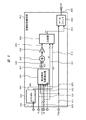
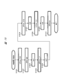
- FIG. 1 is a schematic diagram showing a configuration example of a signal transmission system according to Embodiment 1 of the present invention.
- FIG. 1 shows a configuration example of a signal transmission system that performs wired transmission on the same substrate.
- the substrate 101 includes a signal processing ASIC (Application Specific Integrated Circuit) 102 having a waveform equalization function, a communication ASIC 103 having a waveform equalization function, and a connector 104.
- the ASIC 102 and the ASIC 103 communicate with each other via a wiring on the substrate 101, and the ASIC 103 communicates with another device through the connector 104.
- ASIC Application Specific Integrated Circuit
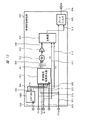
- FIG. 2 is a schematic diagram showing another configuration example of the signal transmission system according to Embodiment 1 of the present invention.
- FIG. 2 shows a configuration example of a signal transmission system in which the communication in FIG. 1 is performed not only on the same board but also on different boards and a repeater is mounted.
- the substrate 201 mounts the signal processing ASIC 204, the repeater 205, and the connector 208, and the substrate 203 mounts the signal processing ASIC 207, the repeater 206, and the connectors 209 and 210.
- the substrate 202 is connected to the substrates 201 and 203 via connectors 208 and 209, respectively.
- the signal processing ASIC 204 communicates with another device connected to the end of the connector 210 through the communication ASIC 207.
- the signal output from the ASIC 204 is relayed to the board 202 by the relay 205 and transmitted to the relay 206 via the wiring on the board 202.
- the repeater 206 relays the transmitted signal to the communication ASIC 207, and the ASIC 207 transmits the relayed signal to an external device through the connector 210.
- a signal received by the ASIC 207 from the external device through the connector 210 is received by the ASIC 204 via the repeater 206, the substrate 202, and the repeater 205 in this order.
- each of the ASICs 102, 103, 204, 207 and the repeaters 205, 206 is a signal transmission device in which a transmitter and a receiver are mounted on one semiconductor chip, for example.
- the substrate 202 is a backplane or the like
- each of the substrates 201 and 203 is a card or the like that can be mounted on the backplane.
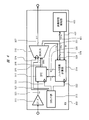
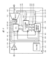
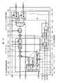
- FIG. 3 is a block diagram illustrating a configuration example of each signal transmission device studied as a premise of the first embodiment in the signal transmission system of FIGS. 1 and 2.
- the semiconductor chips (signal transmission devices) 301 and 303 in FIG. 3 correspond to the ASICs 102 and 103 in FIG. 1, respectively, and the transmission path 302 in FIG. 3 corresponds to the wiring on the substrate 101 in FIG.
- the semiconductor chips 301 and 303 in FIG. 3 correspond to the repeaters 205 and 206 in FIG. 2, respectively, and the transmission path 302 in FIG. 3 corresponds to the wiring on the substrate 202 in FIG.
- the semiconductor chip (signal transmission device) 301 includes a transmitter 304 and a signal processing unit 305
- the semiconductor chip (signal transmission device) 303 includes a receiver 309 and a signal processing unit 310.
- a signal transmitted from the transmitter 304 of the semiconductor chip 301 is transmitted through the transmission path 302 and received by the receiver 309 of the semiconductor chip 303.
- each of the semiconductor chips 301 and 304 is configured to include one of a transmitter and a receiver for convenience, but actually includes both a transmitter and a receiver.
- the transmitter 304 includes a feed forward equalizer (hereinafter referred to as FFE) 307, a multiplexer 306, and a PLL (Phase Locked) Loop) 308.
- the receiver 309 includes a continuous time linear equalizer (hereinafter referred to as CTLE (Continuous Time Linear Equalizer)) 311, a decision feedback equalizer (hereinafter referred to as DFE (Decision Feedback Equalizer)) 312, and a clock source. 313, a filter coefficient calculation unit 314, and a demultiplexer 315.
- CTLE Continuous Time Linear Equalizer
- DFE Decision Feedback Equalizer
- the signal processing unit 305 performs predetermined signal processing and transmits a parallel data signal to the transmitter 304 as necessary.
- the multiplexer (parallel-serial converter) 306 receives the parallel data signal and converts the parallel data signal into a serial data signal in synchronization with the clock from the PLL 308.
- the FFE 307 receives the serial data signal, processes the data signal into a signal that emphasizes the high frequency side in advance, and transmits the signal to the transmission path 302. Specifically, the FFE 307 performs waveform equalization so as to reduce the gain on the low frequency side, for example.
- the data signal 315 that has passed through the transmission path 302 is received by the receiver 309 in the semiconductor chip 303.
- the data signal transmitted from the transmitter 304 is attenuated through the transmission path 302.
- the CTLE 311 performs waveform equalization by amplifying the high-frequency side of the received data signal, and outputs the signal (Vo) 320 on which waveform equalization has been performed to the DFE 312.
- the DFE 312 performs waveform equalization on the signal (Vo) 320 such that the low frequency side is attenuated and the high frequency side is amplified in accordance with the filter coefficient (Wi) 330 from the filter coefficient calculation unit 314 and amplified. After that, logical determination (positive / negative determination) is performed.
- the DFE 312 sequentially latches the logical data (DTS) 325 that is the result of the logical determination (positive / negative determination) in response to the clock 321 from the clock source 313, and outputs it as a serial data signal. Further, the DFE 312 compares not only the logical determination of data but also the filter convergence target value (target peak value) (TGT) 331 from the filter coefficient calculation unit 314 and the peak value of the signal subjected to waveform equalization by the DFE 312. Then, a filter convergence target value error (ERRs) 326 is output.
- DTS logical data
- TGT filter convergence target value
- ERRs filter convergence target value error
- the demultiplexer (serial / parallel converter) 315 receives the logical data (DTS) 325 and the filter convergence target value error (ERRs) 326, and converts these serial signals into parallel signals using the clocks 323 and 324 from the clock source 313. To do. As a result, the demultiplexer 315 outputs logical data (DTP) 327 as a parallel data signal, logical data (DTp) 328 as a part thereof, and a filter convergence target value error (ERRp) 329 as a parallel signal. To do.
- DTP logical data
- DTp logical data
- ERRp filter convergence target value error
- the demultiplexer 315 outputs a parallel signal every 32 cycles of the clock 324.
- the logical data (DTP) 327 is configured by, for example, a 32-bit area
- the logical data (DTp) 328 is configured by a predetermined adjacent multiple-bit area in the 32-bit area.
- the number of bits of the plurality of bits is determined based on the number of taps of the DFE 312, for example.
- the filter coefficient calculation unit 314 receives the logical data (DTp) 328 and the filter convergence target value error (ERRp) 329.
- the logical data (DTS) 325 and the filter convergence target value error (ERRs) 326 from the DFE 312 are input to the filter coefficient calculation unit 314 via the demultiplexer 315.
- the filter coefficient calculation unit 314 operates with the clock 322 from the clock source 313, receives the logical data (DTp) 328 and the filter convergence target value error (ERRp) 329, and sets the filter coefficient (Wi) 330 of the DFE 312 by an adaptive algorithm. calculate.
- an LMS (Least) Mean Square) algorithm is typically known.
- the filter coefficient calculation unit 314 also calculates a filter convergence target value (target peak value) (TGT) 331.
- the filter convergence target value (target peak value) (TGT) 331 can be, for example, an average value of the signal amplitude after waveform equalization (V (Z 0 ) in FIG. 16 described later). That is, when waveform equalization is performed, the signal amplitude after waveform equalization is ideally constant regardless of the data pattern. Therefore, the filter coefficient calculation unit 314 detects the average value of the signal amplitude and uses it as a target value so that the instantaneous amplitude value approaches the target value (that is, the target value error is minimized). An arithmetic process that converges the filter coefficients may be performed using an adaptive algorithm.
- the signal processing unit 310 performs predetermined signal processing using the logical data (DTP) 327.
- DTP logical data
- the signal processing unit 310 performs error correction or the like on the logical data (DTP) 327 and then stores the logical data in the semiconductor chip 303.
- the relaying process is performed via a transmitter (not shown).
- FIG. 16 is a schematic diagram illustrating a schematic configuration example of the DFE in FIG.
- the DFE 312 receives the signal (Vo) 320 from the CTLE 311 and feeds back the multiplication result of the filter coefficient (Wi) 330 and the logical data of the past signal (Vo) 320 to the signal.
- Waveform equalization Here, the case of 3 taps is taken as an example, and the multiplier block 1601 outputs each logical data (Z in the previous to third cycles) output from the determiner with latch 1602, the latch circuit 1603, and the latch circuit 1604, respectively. ⁇ 1 , Z ⁇ 2 , Z ⁇ 3 ) and the first to third tap filter coefficients W1 to W3, respectively.
- the adder block 1600 performs waveform equalization by adding the multiplication result from the multiplier block 1601 to the signal (Vo) 320. This eliminates intersymbol interference (ISI) components.
- ISI intersymbol interference
- the DFE 312 outputs the logical data of the signal (Vo) 320 by performing logical determination (positive / negative determination) and latching of the waveform equalized signal (V (Z 0 )) by the determination unit 1602 with latch.
- the logical data is sequentially transferred to the latch circuit 1603 and the latch circuit 1604 in synchronization with the clock.
- the DFE 312 detects the difference between the wave height value of the waveform equalized signal and the filter convergence target value (target wave height value) (TGT) 331 by the error detector 1605, so that the filter convergence target value error (ERRs) 326 is detected. Is output after adjusting the timing by the delay circuit 1606.
- the CTLE 311 in FIG. 3 is an analog amplifier and has a limited input / output range that can be linearly amplified.
- the power supply voltage decreases, and the input / output range in which linearity can be secured is becoming narrower.
- the power supply voltage is 1 V or less
- the input range in which linear operation is possible with a general resistive load type amplifier is only about 200 to 300 mV, for example.
- the loss in the transmission path 302 on the substrate tends to increase on the high frequency side, and the signal level difference between the low frequency side and the high frequency side increases as the speed increases.
- a signal level difference of 30 dB or more can occur.
- the signal level increases to, for example, 500 mV or more, and the linear operation of the CTLE 311 becomes difficult.
- the signal (Vo) 320 from the CTLE 311 includes components added to the signal due to the influence of nonlinearity in addition to components added to the signal by ISI.
- the component due to ISI depends on the data pattern because it follows the frequency characteristics of the signal path, and the component due to non-linearity depends on the signal level (and hence the frequency of the signal), so it also depends on the data pattern. Both depend on the data pattern, but because the causes are different from each other, the same trend does not occur.
- the filter coefficient calculation unit 314 obtains a correlation between the data pattern (that is, each bit of the logical data (DTp) 328) and the filter convergence target value error (ERRp) 329, and uses the LMS algorithm or the like.
- a filter coefficient (Wi) 330 is calculated.
- the filter coefficient calculation unit 314 is difficult to extract only the ISI component from the correlation result, for example, because the data pattern dependency of the component due to ISI and the component due to nonlinearity do not have the same tendency.
- an error in the calculation result of the filter coefficient (Wi) 330 (that is, an error with respect to an ideal waveform equalization amount necessary for eliminating the ISI component) may occur.
- an error when the filter coefficient (Wi) 330 is automatically adjusted in accordance with environmental fluctuations such as temperature and power supply voltage fluctuations becomes large.
- the waveform equalization amount is deviated, the ISI component cannot be sufficiently eliminated, and there is a possibility that jitter increases (for example, eye reduction in a so-called eye pattern).
- a signal affected by non-linearity is detected, and only a linearly operating signal is used for calculation of the filter coefficient (Wi) 330. Specifically, by not using the low-frequency signal for calculating the filter coefficient (Wi) 330, the influence of nonlinearity is suppressed and the filter coefficient (Wi) 330 is optimally converged.
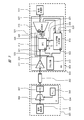
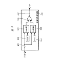
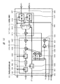
- FIG. 4 is a block diagram illustrating a configuration example of a main part of the signal transmission device according to the first embodiment in the signal transmission system of FIGS. 1 and 2.
- the signal transmission device according to the first embodiment is configured to include a receiver 309 as in the semiconductor chip (signal transmission device) 303 of FIG. 3. As shown in FIG. The configuration is different from FIG.
- the receiver 309 illustrated in FIG. 4 further includes a nonlinearity detection unit 400 with respect to the receiver 309 of FIG.
- the non-linearity detection unit 400 monitors the logical data from the DFE, detects a data pattern in which n bits (n is an integer of 2 or more) are continuously at the same logical level, and causes the filter coefficient calculation unit 314 to detect the detection. Instructed not to calculate the filter coefficient (Wi) 330 for the selected data pattern.
- the nonlinearity detection unit 400 receives the logical data (DTpp) 401 that is a part of the logical data (DTp) 328 from the demultiplexer 315, and thereby monitors the logical data from the DFE.
- the nonlinearity detection unit 400 looks at the data pattern of the logical data (DTpp) 401 and outputs an enable signal (EN) 402 that instructs the filter coefficient calculation unit 314 whether or not to calculate the filter coefficient.
- the loss of the transmission path 302 tends to be low on the low frequency side and high on the high frequency side. Therefore, if a low frequency signal is detected, a signal that is not linearly amplified can be detected.
- the low frequency signal is a case where the same data continues, for example, in the case of a data pattern such as 111..., 000.
- FIG. 5 is a circuit diagram showing a configuration example of the nonlinearity detection unit in FIG.
- a case where the logical data (DTpp) 401 is 4 bits is taken as an example.
- the nonlinearity detection unit 400 controls the enable signal (EN) 402 to the “L” level (negate) when the comparison results match, and sets the enable signal (EN) 402 to “H” when they do not match. Control to level (assert).
- the nonlinearity detection unit 400 includes a NOR gate 500, comparators 501 and 502, and predetermined data patterns 503 and 504.
- the data pattern of the logical data (DTpp) 401 is “0000”
- the output of the comparator 501 is at the “H” level
- the enable signal (EN) 402 output from the NOR gate 500 is at the “L” level.
- the data pattern of the logical data (DTpp) 401 is “1111”
- the output of the comparator 502 becomes “H” level
- the enable signal (EN) 402 becomes “L” level.
- the filter coefficient calculation unit 314 performs the filter coefficient (Wi) 330 and the filter convergence target value (TGT) for the logical data (DTp) 328 corresponding to the logical data (DTpp) 401 according to the 'L' level. ) The calculation of 331 is stopped.
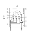
- FIG. 7 is a circuit diagram showing another configuration example of the nonlinearity detection unit in FIG. 7 receives the logical data (DTpp) 401, the logical data (Z 0 ) of the current cycle included in the logical data (DTpp) 401, and the previous to (n ⁇ 1) ) Each logical data (Z ⁇ 1 to Z ⁇ 3 ) in the previous cycle is compared with each other.
- the nonlinearity detection unit 400 controls the enable signal (EN) 402 to the “L” level (negate) when the comparison results match, and sets the enable signal (EN) 402 to “H” when they do not match. Control to level (assert).
- the nonlinearity detection unit 400 includes an OR gate 700 and three XOR gates 701, 702, and 703.
- the XOR gates 701, 702, and 703 include the logical data (Z 0 ) in the current cycle included in the logical data (DTpp) 401 and the logical data (Z ⁇ 1 to Z ⁇ in the previous to third previous cycles). 3 ) are compared with each other.
- the OR gate 700 outputs the 'L' level as the enable signal (EN) 402 only when all the comparison results match (that is, when the data pattern is “1111” or “0000”).
- the filter coefficient calculation unit 314 stops the calculation of the filter coefficient for the logical data (DTp) 328 corresponding to the logical data (DTpp) 401 according to the “L” level.
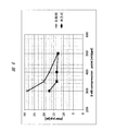
- FIG. 6 is an explanatory diagram showing an example of the effect when the receivers of FIGS. 4 and 5 are used.
- FIG. 6 shows a simulation using a 28 Gbps NRZ signal for a system having a loss of 35 dB at the Nyquist frequency with the bit number (n) of the data patterns 503 and 504 of the nonlinearity detection unit 400 being 4 bits. It is a result.
- the cross marks indicate the results when the nonlinearity detection unit 400 is not provided, and the results when the nonlinearity detection unit 400 is provided.
- the horizontal axis is 1 dB compression point, which is an index indicating the linearity of CTLE 311, and the lower the linearity, the worse the linearity.
- the vertical axis represents the jitter of the signal after waveform equalization in DFE 312 (V (Z 0 ) in FIG. 16).
- the jitter can be reduced by the filter coefficient (Wi) 330 converging to an appropriate value even under poor linearity conditions. That is, by using the signal transmission device and the signal transmission system according to the first embodiment, the filter constant of the DFE 312 can be optimally maintained regardless of the linearity of the amplifier (CTLE 311) in the receiver 309, and jitter can be reduced. Etc. can be realized.
- the number of bits (n) of the data patterns 503 and 504 for example, assuming that the equalization amount in the DFE 312 is 20 dB and the loss increases with a constant slope (dB / Hz), the Nyquist frequency of 28 Gbps is obtained in 32 GFC. At 1/14, the loss becomes 0 dB. In this case, the number of bits (n) of the data patterns 503 and 504 is appropriately about 4 bits that is 1/16 of the data rate.
- the number of bits (n) of the data patterns 503 and 504 is not particularly limited to this and may be 2 bits or more. However, if the number of bits is too small, the signal on the high frequency side is unnecessarily filtered, resulting in poor convergence of the filter coefficient. If the number of bits is too large, the filtering that is originally necessary for some of the signals on the low frequency side is performed. This is not done, and there is a risk of increasing jitter. Therefore, for example, the frequency of the boundary where nonlinearity occurs in the CTLE 311 may be estimated in consideration of the characteristics of the transmitter 304 and the transmission path 302, and the number of bits corresponding to the frequency near the boundary may be determined.
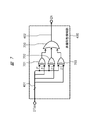
- FIG. 8 is a block diagram showing a configuration example of the main part of the signal transmission apparatus according to the second embodiment.
- FIG. 8 shows a configuration example of the receiver 309 included in the signal transmission device, as in the case of FIG.
- the receiver 309 in FIG. 8 includes a CTLE 311, a DFE 312, a clock source 313, a filter coefficient calculation unit 314, a demultiplexer 315, and a nonlinearity detection unit 800 as in the case of the first embodiment (FIG. 4).
- the configuration and operation of the nonlinearity detection unit 800 are different from those in the first embodiment, and the input / output signals with other circuit blocks are also slightly different. Hereinafter, description will be made focusing on this difference.
- the demultiplexer 315 becomes a part of the logical data (DTp) 328 in addition to the logical data (DTP) 327, the logical data (DTp) 328, and the filter convergence target value error (ERRp) 329 similar to the case of FIG.
- the logical data (DTpp) 801 is output.
- the filter coefficient calculation unit 314 performs the filter coefficient (Wi) 330 and the filter convergence target value (TGT) when the enable signal (EN) 804 from the nonlinearity detection unit 800 is at the “H” level. ) 331 is calculated, and when the enable signal (EN) 804 is at the “L” level, the calculation is stopped.
- the filter coefficient calculation unit 314 outputs the calculated filter coefficient (Wi) 330 and the filter convergence target value (TGT) 331 to the DFE 312, and further outputs the calculated filter coefficient (Wi) 802 to the nonlinearity detection unit 800.
- a filter convergence target value (TGT) 803 is output.
- the nonlinearity detection unit 800 includes a signal (Vo) 320 from the CTLE 311, a logical data (DTpp) 801 from the demultiplexer 315, a filter coefficient (Wi) 802 and a filter convergence target value (TGT) from the filter coefficient calculation unit 314. 803, and operates in synchronization with clocks 805 and 806 from the clock source 313.
- the clock 805 is a clock having the same phase as the clock 321 to the DFE 312, and the clock 806 is an internal operation clock.
- the nonlinearity detection unit of the first embodiment described above detects logical data in which the same logical level is continued for n bits as logical data in which nonlinearity occurs.
- whether or not nonlinearity actually occurs may vary depending on, for example, the length of the transmission path 302.
- the length of the transmission path 302 may vary depending on the mounting position.
- the nonlinearity detection unit 800 in FIG. 8 calculates the filter coefficient for each frequency (on the high frequency side and the low frequency side) in the same manner as the DFE 312 and the filter coefficient calculation unit 314, and the average value of the filter coefficient and the filter coefficient By comparing with the filter coefficient (Wi) 802 from the calculation unit 314, it is determined whether or not the CTLE 311 is operating linearly.
- the enable signal (EN) 804 is kept at the “H” level even when the same logic level continues for n bits, and is not operating linearly.
- the enable signal (EN) 804 is controlled to the 'L' level.
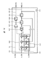
- FIG. 9 is a block diagram illustrating a configuration example of the nonlinearity detection unit in FIG. 9 includes a controller 900, a frequency-specific coefficient detector 901, an adder 902, an amplifier 903, a comparator 904, and a data filter 905.
- the controller 900 operates in synchronization with the clock 806, outputs a detection enable signal (DEN) 906 to the coefficient detector 901 for each frequency for a certain period, and outputs a predetermined threshold value (a predetermined threshold value) to the comparator 904.
- DEN detection enable signal
- Wth predetermined threshold value
- the frequency-specific coefficient detector 901 includes a signal (Vo) 320 from the CTLE 311, a filter coefficient (Wi) 802, and a demultiplexer 315 while the detection enable signal (DEN) 906 is at the “H” level (asserted). In response to the logical data (DTpp) 801, the detection operation is performed in synchronization with the clock 805.
- the frequency-specific coefficient detector 901 includes a dummy decision feedback equalizer and a dummy filter coefficient calculator that reflect the configurations of the DFE 312 and the filter coefficient calculator 314, respectively, as shown in detail in FIG. The filter coefficient corresponding to the tap eye is calculated and held.
- the frequency-specific coefficient detector 901 targets the data pattern in which the logic data of the signal (Vo) 320 from the CTLE 311 is m bits (m is an integer of 2 or more) continuously at the same logic level.
- the dummy filter coefficient (W1l) 907 for the first tap is calculated.
- the frequency-specific coefficient detector 901 calculates a dummy filter coefficient (W1h) 908 for the first tap on the high frequency side for a data pattern that does not have the same logic level continuously for 2 bits or more.
- the logical data (DTpp) 801 from the demultiplexer 315 is used here as the logical data of the signal (Vo) 320 from the CTLE 311. For example, in the case of 3 bits, if the logical data (DTpp) 801 is “000” or “111”, it is determined as a low frequency, and if it is “010” or “101”, it is determined as a high frequency.
- the adder 902 and the amplifier 903 average the low frequency side dummy filter coefficient (W1l) 907 and the high frequency side dummy filter coefficient (W1h) 908, thereby calculating an average value calculation unit that calculates the dummy filter coefficient 909. It becomes. That is, the adder 902 adds the dummy filter coefficient (W1l) 907 on the low frequency side and the dummy filter coefficient (W1h) 908 on the high frequency side, and the amplifier 903 halves the addition result.
- the filter coefficient (Wi) 802 from the filter coefficient calculation unit 314 is an optimal value.
- the dummy filter coefficient 909 should be a value that is not significantly different from the filter coefficient (W1) 911 of the first tap of the filter coefficient (Wi) 802.
- the CTLE 311 cannot operate linearly, the dummy filter coefficient 909 and the filter coefficient (W1) 911 are greatly different.
- the comparator 904 generates the nonlinearity detection signal (CPo) 910 when the absolute value of the difference between the dummy filter coefficient 909 and the filter coefficient (W1) 911 is larger than a predetermined threshold value (Wth) 912.
- the “H” level is output, and if not, the “L” level is output as the non-linearity detection signal (CPo) 910.
- the “H” level of the non-linearity detection signal (CPo) 910 indicates that the CTLE 311 cannot operate linearly.
- the data filter 905 operates when the nonlinearity detection signal (CPo) 910 is at the “H” level, and stops operating when it is at the “L” level.
- the data filter 905 monitors the logical data (DTpp) 801 from the DFE 312 via the demultiplexer 315, and displays a data pattern in which n bits are continuously at the same logical level, and the nonlinearity detection signal (CPo) 910 is 'H'. 'Detect if level.
- the data filter 905 outputs “L” level as the enable signal (EN) 804 during the period when the data pattern is detected, and “H” as the enable signal (EN) 804 during the period when it is not detected. Output level.
- the filter coefficient calculation unit 314 stops the calculation of the filter coefficient for the logical data (DTp) 328 corresponding to the logical data (DTpp) 801 according to the “L” level of the enable signal (EN) 804. .
- the filter coefficient calculation unit 314 calculates a filter coefficient when the enable signal (EN) 804 is at the “H” level.
- the data filter 905 outputs “L” level as the enable signal (EN) 804 when the logical data (DTpp) 801 is “0000” or “1111”, as in the first embodiment. To do.
- the number of high frequency / low frequency discrimination bits (m) in the frequency-specific coefficient detector 901 and the low frequency discrimination bit number (n) in the data filter 905 are not necessarily the same. It does not have to be.
- the presence or absence of the nonlinear operation is determined using the filter coefficient of the first tap of the DFE 312, but the filter coefficients of other taps are used instead of the first tap or in addition to the first tap. Is also possible.
- the use of the first tap in particular makes it possible to determine the presence or absence of nonlinear operation with the highest sensitivity.
- FIG. 10 is a circuit diagram showing a configuration example of the frequency-specific coefficient detector in FIG.
- the frequency coefficient detector 901 includes the dummy DFE 1016 described in FIG. 9 and a dummy filter coefficient calculation unit 1017.
- the dummy DFE 1016 includes a sample and hold circuit 1000, an analog / digital converter 1001, delay circuits 1002 and 1003, multipliers 1004, 1005 and 1009, adders 1006 and 1007, and an amplifier 1008.
- the dummy filter coefficient calculation unit 1017 includes a multiplier 1011, a selector 1012, and integrators 1014 and 1015. In FIG. 10, a case where a 2-tap DFE is used is taken as an example.
- the sample hold circuit 1000 samples the signal (Vo) 320 from the CTLE 311 with the clock 805, and the analog-digital converter 1001 converts the sampled signal into a digital value.
- the phase of the clock 805 is the same as that of the clock 321 for the DFE 312, but the frequency may be less than or equal to the frequency of the clock 321 for the DFE 312. That is, the dummy DFE 1016 may be operated so as to thin out the operation of the DFE 312.
- the delay circuit 1002 delays the digital value from the analog-digital converter 1001 with the clock 805 and outputs it to the adder 1006.
- the delay circuit 1003 delays the logical data (DTpp) 801 from the demultiplexer 315 with the clock 805 and outputs it.
- the delay circuits 1002 and 1006 output the digital value of the signal (Vo) 320 in the current cycle from the delay circuit 1002, and the signal (Vo) 320 in the current cycle and the past cycle.
- the timing at which the logic data (DTpp) 801 is output from the delay circuit 1003 coincides. Since the logical data (DTpp) 801 is generated by the DFE 312 and input to the dummy DFE 1016 via the demultiplexer 315, such timing adjustment is performed.
- the multipliers 1004 and 1005 and the adder 1006 are feedback units that perform waveform equalization.
- the multipliers 1004 and 1005 are connected to the logical data (Z ⁇ 1 and Z ⁇ 2 ) of the past cycle (here, the previous and second previous cycles) included in the logical data (DTpp) 801 from the delay circuit 1003.
- the filter coefficient (Wi) 802 (here, the first tap and the second tap) from the filter coefficient calculation unit 314 is multiplied.
- the adder 1006 adds the digital value (D (Z 0 )) from the delay circuit 1002 and the multiplication result from the multipliers 1004 and 1005, so that the signal (Vo) 320 (the digital value thereof) of the current cycle is added. Waveform equalization is performed on (D (Z 0 )).
- the amplifier 1008, the multiplier 1009, and the adder 1007 serve as an error calculation unit that calculates an error between the peak value after waveform equalization and the target peak value.
- the amplifier 1008 multiplies the logical data (Z 0 ) (positive / negative data) of the current cycle included in the logical data (DTpp) 801 from the delay circuit 1003 by ⁇ 1, and the multiplier 1009 calculates the output of the amplifier 1008 and the filter
- the filter convergence target value (target peak value) (TGT) 803 from the coefficient calculation unit 314 is multiplied.
- the adder 1007 adds the digital value after waveform equalization from the adder 1006 and the digital value from the multiplier 1009 to calculate an error between the peak values of both.
- the multiplier 1011 outputs the logical data (Z ⁇ 1 ) of the past cycle (here, the previous cycle) included in the logical data (DTpp) 801 from the delay circuit 1003. And the digital value from the adder 1007 are multiplied.
- the difference between the peak value of the signal (Vo) 320 and the filter convergence target value (TGT) 803 can be correlated with the logical data of the previous cycle, and 1 is obtained by integrating the result.
- the filter coefficient at the tap can be calculated.
- the selector (selection unit) 1012 selects one of the integrators 1014 and 1015 according to the logical data (DTpp) 801 from the delay circuit 1003, and the digital value from the multiplier 1011 is sent to the selected integrator. Output. Specifically, the selector 1012 indicates that the logical data (DTpp) 801 is “000” or “111” (in other words, the logical data of the signal (Vo) 320 from the DFE 312 is the same logical level for m bits continuously.
- the integrator 1014 is selected. That is, the selector 1012 outputs the digital value from the multiplier 1011 for the data pattern on the low frequency side to the integrator 1014.
- the selector 1012 when the logical data (DTpp) 801 is “010” or “101” (in other words, the logical data of the signal (Vo) 320 from the DFE 312 is not continuously at the same logical level for 2 bits or more. Case), integrator 1015 is selected. That is, the selector 1012 outputs the digital value from the multiplier 1011 targeted for the high frequency side data pattern to the integrator 1015. Note that the selector 1012 does not output to the integrators 1014 and 1015 when the data pattern of the logical data (DTpp) 801 is other than these.
- the integrator 1014 integrates the digital value for the data pattern on the low frequency side from the selector 1012 in synchronization with the clock 805 during the period when the detection enable signal (DEN) 906 is at the “H” level.
- the frequency side dummy filter coefficient (W1l) 907 is calculated.
- the integrator 1015 integrates the digital value for the data pattern on the high frequency side from the selector 1012 in synchronism with the clock 805 during the period in which the detection enable signal (DEN) 906 is at the “H” level.
- the dummy filter coefficient (W1h) 908 is calculated. Further, the integrators 1014 and 1015 hold the integration results while the detection enable signal (DEN) 906 is at the ‘L’ level.
- FIG. 11 is a circuit diagram showing a configuration example of the data filter in FIG.
- a data filter 905 of FIG. 11 includes an OR gate 1100 and an inverter 1101 in addition to the NOR gate 500, the comparators 501 and 502, and the data patterns 503 and 504 similar to those in FIG. Similar to the case of FIG. 5, the comparator 501 compares the logical data (DTpp) 801 with the data pattern 503 “0000”, and the comparator 502 compares the logical data (DTpp) 801 with the data pattern “1111”. 503 is compared.
- the NOR gate 500 outputs the ‘L’ level when the data pattern of the logical data (DTpp) 801 is “0000” or “1111”.
- the inverter 1101 inverts the nonlinearity detection signal (CPo) 910.
- the OR gate 1100 is when the output of the inverter 1101 is at the “L” level (that is, when the nonlinearity detection signal (CPo) 910 is at the “H” level), and when the output of the NOR gate 500 is at the “L” level.
- the “L” level is output as the enable signal (EN) 804.
- FIG. 12 is a circuit diagram showing another configuration example of the data filter in FIG.
- the data filter 905 in FIG. 12 includes an OR gate 1200 and an inverter 1201 in addition to the XOR gates 701, 702, and 703 similar to those in FIG.
- the XOR gates 701, 702, and 703 operate with the logical data (DTpp) 801 as input, as in the case of FIG.
- the inverter 1201 inverts the nonlinearity detection signal (CPo) 910.
- the OR gate 1200 receives the outputs of the XOR gates 701, 702, and 703, and additionally receives the output of the inverter 1201.
- the OR gate 1200 enables the enable signal when the nonlinearity detection signal (CPo) 910 is at the “H” level and the data pattern of the logical data (DTpp) 801 is “0000” or “1111”. (EN) Output 'L' level as 804.
- the data pattern to be calculated for the filter coefficient can be determined more accurately. Therefore, the jitter may be further reduced.
- FIG. 13 is a block diagram showing a configuration example of the main part of the signal transmission apparatus according to the third embodiment.
- FIG. 13 shows a configuration example of the nonlinearity detection unit 800 in the receiver 309 included in the signal transmission device, as in FIG.
- the nonlinearity detection unit 800 shown in FIG. 13 differs from the configuration example of FIG. 9 in the configuration and operation of the controller 1300 and the frequency-specific coefficient detector 1301.
- the controller 1300 outputs logical data for detection (DPN) 1302 in addition to the detection enable signal (DEN) 906 similar to the case of FIG.
- the frequency coefficient detector 1301 detects a filter coefficient for each frequency based on the detection logic data (DPN) 1302.
- an analog-digital converter 1001 is used in the frequency-specific coefficient detector 901 in FIG. 10. Since the analog-digital converter 1001 is required to operate at high speed, there is a risk of increasing power consumption and complicating the circuit. Therefore, it is desirable not to use an analog-digital converter. However, in this case, it is necessary to perform waveform equalization on the analog signal in real time. In other words, when the analog-digital converter 1001 is used, the analog signal of the current cycle is converted into a digital value, and then a delay is added. Waveform equalization can be performed after waiting for logical data of the past cycle. Adding a delay to the signal itself is not easy.
- the controller 1300 generates the low-frequency side data pattern and the high-frequency side data pattern as described in the second embodiment, and generates the generated data patterns in different periods.
- the frequency-specific coefficient detector 1301 speculatively executes the operations up to immediately before the final stage integrators (1407 and 1408 in FIG. 14 described later) based on the detection logic data (DPN) 1302, and performs actual logic processing.
- the integrator is operated.
- FIG. 15 is a flowchart showing an example of the operation sequence of the controller in FIG.
- a case where the detection logical data (DPN) 1302 is 3 bits is taken as an example.
- the controller 1300 sets the detection logic data (DPN) 1302 to “000” (step S1501), sets the detection enable signal (DEN) 906 to the “H” level, and sets the coefficient detector for each frequency 1301. Operate (step S1502).
- the controller 1300 operates the coefficient detector for each frequency 1301 for a certain period of time to detect a peak value error or the like when a data pattern of “000” is assumed (step S1503).
- the controller 1300 sets the detection logical data (DPN) 1302 to “111” (step S1504), operates the frequency-specific coefficient detector 1301 for a certain period of time, and assumes a data pattern of “111”. In this case, a peak value error or the like is detected (step S1505). Subsequently, the controller 1300 sets the detection logical data (DPN) 1302 to “010” (step S1506), operates the frequency-specific coefficient detector 1301 for a certain period of time, and assumes a data pattern of “010”. In this case, a peak value error or the like is detected (step S1507).
- the controller 1300 sets the detection logical data (DPN) 1302 to “101” (step S1508), operates the frequency-specific coefficient detector 1301 for a certain period of time, and assumes a data pattern of “101”. In this case, a peak value error or the like is detected (step S1509). Thereafter, the controller 1300 sets the detection enable signal (DEN) 906 to the 'L' level and stops the operation of the frequency coefficient detector 1301 (step S1510). As described above, the controller 1300 includes the detection logical data (“000” or “111”) in which the same logical level continues for m bits and the detection logical data (“010” in which the same logical level does not continue for 2 bits or more). "Or” 101 ”) are output in different periods.
- FIG. 14 is a circuit diagram showing a configuration example of the frequency-specific coefficient detector in FIG.
- the frequency-specific coefficient detector 1301 roughly indicates that the filter coefficient when the detection logical data (DPN) 1302 matches the logical data (DTpp) 801 input from the DFE 312 via the demultiplexer 315. Is calculated.
- the frequency-specific coefficient detector 1301 includes a dummy DFE 1419 and a dummy filter coefficient calculation unit 1420.
- the dummy DFE 1419 includes adders 1400 and 1401, a determiner 1402, a latch circuit 1403, multipliers 1409, 1410 and 1414, an amplifier 1413, and digital / analog converters 1411, 1412 and 1415.
- the dummy filter coefficient calculation unit 1420 includes a multiplier 1404, a delay circuit 1415, a selector 1406, integrators 1407 and 1408, and an integrator control unit 1421.
- the integrator control unit 1421 includes a delay circuit 1416, a comparator 1417, and an AND gate 1418.
- Multipliers 1409 and 1410, digital-analog converters 1411 and 1412, and adder 1400 serve as a feedback unit that performs waveform equalization.
- Multipliers 1409 and 1410 include respective bits corresponding to the past cycles (here, the previous and second previous cycles) included in the detection logical data (DPN) 1302 from the controller 1300, and a filter coefficient calculation unit.
- the filter coefficient (Wi) 802 from 314 (here, the first tap and the second tap) is multiplied.
- Digital-to-analog converters 1411 and 1412 convert digital values resulting from multiplication by multipliers 1409 and 1410 to analog signals (filter constants), respectively.
- the adder 1400 performs waveform equalization by adding the analog signals from the digital-analog converters 1411 and 1412 to the signal (Vo) 320 from the CTLE 311.
- the amplifier 1413, the multiplier 1414, the digital-analog converter 1415, and the adder 1401 serve as an error detection unit that detects an error between the peak value after waveform equalization and the target peak value.
- the amplifier 1413 multiplies the bit (positive / negative data) corresponding to the current cycle included in the detection logic data (DPN) 1302 by ⁇ 1, and the multiplier 1414 outputs the output from the amplifier 1413 and the filter coefficient calculation unit 314.
- the filter convergence target value (target peak value) (TGT) 803 is multiplied.
- the digital / analog converter 1415 converts the digital value from the multiplier 1414 into an analog signal (that is, an analog signal corresponding to the target peak value).
- the adder 1401 adds the analog signal from the adder 1400 (that is, the analog signal after waveform equalization) and the analog signal from the digital-analog converter 1415, and outputs the difference signal.
- the determiner 1402 determines whether the difference signal from the adder 1401 is positive or negative (that is, determines whether the analog signal after waveform equalization is larger or smaller than the target), and the latch circuit 1403 displays the determination result at the clock 805. Latch.
- the multiplier 1404 includes the logic data (Z ⁇ 1 ) of the past cycle (here, the previous cycle) included in the detection logic data (DPN) 1302 and the latch circuit. Multiply the logical data from 1403.
- the delay circuit 1405 delays the logical data from the multiplier 1404 with the clock 805.
- the selector (selection unit) 1406 outputs the logic data from the delay circuit 1405 to the integrator 1407 when the detection logic data (DPN) 1302 is a low frequency data pattern (“000” or “111”). .
- the selector 1406 outputs the logical data from the delay circuit 1405 to the integrator 1408 when the detection logical data (DPN) 1302 is a high-frequency data pattern (“010” or “101”).
- the selector 1406 does not output to the integrators 1407 and 1408 when the detection logical data (DPN) 1302 is other than these.
- the delay circuit 1416 delays the logical data (DTpp) 801 input from the DFE 312 via the demultiplexer 315 with the clock 805.
- the comparator 1417 compares the logical data (DTpp) 801 from the delay circuit 1416 with the detection logical data (DPN) 1302 and outputs an 'H' level if they match.
- the AND gate 1418 outputs the “H” level as the integration enable signal (IEN) 1422 when the detection enable signal (DEN) 906 is at the “H” level and the comparator 1417 outputs the “H” level. Is output.
- the timing at which the processing result for the signal (Vo) 320 of the current cycle from the CLTE 311 is output from the delay circuit 1405 by the delay circuits 1405 and 1416 and the logical data of each signal (Vo) 320 in the current cycle and the past cycle The timing at which (DTpp) 801 is output from the delay circuit 1416 coincides.
- the integrator 1407 integrates logic data based on the data pattern on the low frequency side from the selector 1406 in synchronization with the clock 805 in a period in which the integration enable signal (IEN) 1422 is at the “H” level.
- a dummy filter coefficient (W1l) 907 on the low frequency side is calculated.
- the integrator 1408 integrates the logic data based on the data pattern on the high frequency side from the selector 1406 in synchronization with the clock 805 in a period in which the integration enable signal (IEN) 1422 is at the “H” level.
- Side dummy filter coefficient (W1l) 908 is calculated. Further, the integrators 1407 and 1408 hold the integration results while the integration enable signal (IEN) 1422 is at the ‘L’ level.
- speculatively executed data based on the detection logic data (DPN) 1302 has reached the inputs of the integrators 1407 and 1408.
- This data becomes correct data when the detection logical data (DPN) 1302 and the logical data (DTpp) 801 match, and becomes incorrect data when they do not match. Therefore, by identifying this match / mismatch (in other words, whether speculative execution is correct) by the integration enable signal (IEN) 1422, only correct data can be integrated by the integrators 1407, 1408.
- an analog-digital converter is not necessary, so that power consumption can be reduced. In some cases, the circuit can be simplified.
- the present invention made by the present inventor has been specifically described based on the embodiment.
- the present invention is not limited to the embodiment, and various modifications can be made without departing from the scope of the invention.
- the above-described embodiment has been described in detail for easy understanding of the present invention, and is not necessarily limited to one having all the configurations described.
- a part of the configuration of one embodiment can be replaced with the configuration of another embodiment, and the configuration of another embodiment can be added to the configuration of one embodiment. .
Landscapes
- Engineering & Computer Science (AREA)
- Computer Networks & Wireless Communication (AREA)
- Signal Processing (AREA)
- Cable Transmission Systems, Equalization Of Radio And Reduction Of Echo (AREA)
Abstract
Selon l'invention, un égaliseur linéaire de temps continu (CTLE) (311) délivre un second signal qui a subi une égalisation de forme d'onde par amplification du côté fréquence supérieure d'un premier signal d'entrée. Un égaliseur de rétroaction de décision (DFE) (312) effectue une égalisation de forme d'onde sur le second signal d'entrée par utilisation d'un facteur de filtre (Wi) et prend une décision logique sur le second signal ayant subi une égalisation de forme d'onde pour délivrer ainsi en sortie des données logiques du second signal (DTS), et en outre, le DFE (312) détecte une différence entre une valeur maximale du signal ayant subi une égalisation de forme d'onde et une valeur maximale cible (TGT) pour délivrer ainsi en sortie une erreur de valeur cible (ERR). Une unité de calcul de facteur de filtre (314) reçoit les données logiques et l'erreur de valeur cible à partir du DFE (312) et calcule un facteur de filtre (Wi) du DFE (312) par utilisation d'un algorithme adaptatif. Une unité de détection de non-linéarité (400) surveille les données logiques provenant du DFE (312), détecte un motif de données de n bits (où n est un nombre entier égal ou supérieur à deux) ayant successivement le même niveau logique, et donne l'instruction à l'unité de calcul de facteur de filtre (314) de ne pas réaliser le calcul de facteur de filtre pour le motif de données détecté.
Priority Applications (1)
| Application Number | Priority Date | Filing Date | Title |
|---|---|---|---|
| PCT/JP2015/074692 WO2017037836A1 (fr) | 2015-08-31 | 2015-08-31 | Appareil d'émission de signal et système d'émission de signal |
Applications Claiming Priority (1)
| Application Number | Priority Date | Filing Date | Title |
|---|---|---|---|
| PCT/JP2015/074692 WO2017037836A1 (fr) | 2015-08-31 | 2015-08-31 | Appareil d'émission de signal et système d'émission de signal |
Publications (1)
| Publication Number | Publication Date |
|---|---|
| WO2017037836A1 true WO2017037836A1 (fr) | 2017-03-09 |
Family
ID=58187205
Family Applications (1)
| Application Number | Title | Priority Date | Filing Date |
|---|---|---|---|
| PCT/JP2015/074692 WO2017037836A1 (fr) | 2015-08-31 | 2015-08-31 | Appareil d'émission de signal et système d'émission de signal |
Country Status (1)
| Country | Link |
|---|---|
| WO (1) | WO2017037836A1 (fr) |
Cited By (1)
| Publication number | Priority date | Publication date | Assignee | Title |
|---|---|---|---|---|
| CN110719242A (zh) * | 2018-07-13 | 2020-01-21 | 哉英电子股份有限公司 | 均衡器调整装置、均衡器调整方法、接收器及收发系统 |
Citations (5)
| Publication number | Priority date | Publication date | Assignee | Title |
|---|---|---|---|---|
| US20120128055A1 (en) * | 2010-11-19 | 2012-05-24 | Yueming Jiang | Method, apparatus, and system to compensate inter-symbol interference |
| US20120201289A1 (en) * | 2010-09-13 | 2012-08-09 | Abdalla Mohamed | Decision feedback equalizer and transceiver |
| US8396110B1 (en) * | 2010-12-03 | 2013-03-12 | Xilinx, Inc. | Combined decision feedback and linear equalization |
| JP2014143672A (ja) * | 2012-12-25 | 2014-08-07 | Renesas Electronics Corp | 等化器および半導体装置 |
| WO2015125282A1 (fr) * | 2014-02-21 | 2015-08-27 | 株式会社日立製作所 | Appareil de transmission de signaux électriques |
-
2015
- 2015-08-31 WO PCT/JP2015/074692 patent/WO2017037836A1/fr active Application Filing
Patent Citations (5)
| Publication number | Priority date | Publication date | Assignee | Title |
|---|---|---|---|---|
| US20120201289A1 (en) * | 2010-09-13 | 2012-08-09 | Abdalla Mohamed | Decision feedback equalizer and transceiver |
| US20120128055A1 (en) * | 2010-11-19 | 2012-05-24 | Yueming Jiang | Method, apparatus, and system to compensate inter-symbol interference |
| US8396110B1 (en) * | 2010-12-03 | 2013-03-12 | Xilinx, Inc. | Combined decision feedback and linear equalization |
| JP2014143672A (ja) * | 2012-12-25 | 2014-08-07 | Renesas Electronics Corp | 等化器および半導体装置 |
| WO2015125282A1 (fr) * | 2014-02-21 | 2015-08-27 | 株式会社日立製作所 | Appareil de transmission de signaux électriques |
Non-Patent Citations (1)
| Title |
|---|
| JIHONG REN ET AL.: "Precursor ISI Reduction in High-Speed I/O", IEEE SYMPOSIUM ON VLSI CIRCUITS, June 2007 (2007-06-01), pages 134 - 135, XP031142376 * |
Cited By (2)
| Publication number | Priority date | Publication date | Assignee | Title |
|---|---|---|---|---|
| CN110719242A (zh) * | 2018-07-13 | 2020-01-21 | 哉英电子股份有限公司 | 均衡器调整装置、均衡器调整方法、接收器及收发系统 |
| CN110719242B (zh) * | 2018-07-13 | 2024-04-12 | 哉英电子股份有限公司 | 均衡器调整装置、均衡器调整方法、接收器及收发系统 |
Similar Documents
| Publication | Publication Date | Title |
|---|---|---|
| US11398933B2 (en) | Multi-tap decision feed-forward equalizer with precursor and postcursor taps | |
| US9705708B1 (en) | Integrated circuit with continuously adaptive equalization circuitry | |
| US10498562B2 (en) | Electric signal transmission device | |
| US8654884B2 (en) | Channel equalization using application specific digital signal processing in high-speed digital transmission systems | |
| US9294313B2 (en) | Receiver with pipelined tap coefficients and shift control | |
| US8582635B2 (en) | Sparse and reconfigurable floating tap feed forward equalization | |
| US20190353704A1 (en) | Eye opening measurement circuit calculating difference between sigma levels, receiver including the same, and method for measuring eye opening | |
| US20100103998A1 (en) | Decision feedback equalization scheme with minimum correction delay | |
| US7869494B2 (en) | Equalizer circuitry for mitigating pre-cursor and post-cursor intersymbol interference | |
| US11962441B2 (en) | Multi-tap decision feed-forward equalizer with precursor and postcursor taps | |
| WO2008026289A1 (fr) | Circuit de transmission de données et procédé de transmission | |
| WO2008032492A1 (fr) | Procédé d'égalisation de forme d'onde de type à retour négatif de détermination et égalisateur | |
| US8446941B2 (en) | Equalizer employing adaptive algorithm for high speed data transmissions and equalization method thereof | |
| US7590176B2 (en) | Partial response transmission system and equalizing circuit thereof | |
| US7545861B2 (en) | Timing recovery circuit and timing recovery method | |
| US8432960B2 (en) | Digital adaptive channel equalizer | |
| WO2017037836A1 (fr) | Appareil d'émission de signal et système d'émission de signal | |
| WO2019167275A1 (fr) | Égaliseur à retour de décision et récepteur l'utilisant | |
| US8259784B2 (en) | High-speed continuous-time feedback equalizer for serial link receiver | |
| JP5077241B2 (ja) | 等化フィルタおよび歪み補償方法 | |
| CN112491429B (zh) | 通讯接收装置与时脉数据回复方法 | |
| Rao et al. | Correcting the effects of mismatches in time-interleaved analog adaptive FIR equalizers | |
| US10581646B1 (en) | Asynchronous data correction filter | |
| WO2021104382A1 (fr) | Appareil et récepteur d'élimination de dérive de ligne de base | |
| JP2011234010A (ja) | 適応等化回路及び受信回路 |
Legal Events
| Date | Code | Title | Description |
|---|---|---|---|
| 121 | Ep: the epo has been informed by wipo that ep was designated in this application |
Ref document number: 15902958 Country of ref document: EP Kind code of ref document: A1 |
|
| NENP | Non-entry into the national phase |
Ref country code: DE |
|
| 122 | Ep: pct application non-entry in european phase |
Ref document number: 15902958 Country of ref document: EP Kind code of ref document: A1 |
|
| NENP | Non-entry into the national phase |
Ref country code: JP |