WO2017029836A1 - Sensor controller, pointing device, and position detection system - Google Patents
Sensor controller, pointing device, and position detection system Download PDFInfo
- Publication number
- WO2017029836A1 WO2017029836A1 PCT/JP2016/062325 JP2016062325W WO2017029836A1 WO 2017029836 A1 WO2017029836 A1 WO 2017029836A1 JP 2016062325 W JP2016062325 W JP 2016062325W WO 2017029836 A1 WO2017029836 A1 WO 2017029836A1
- Authority
- WO
- WIPO (PCT)
- Prior art keywords
- value
- code
- symbol
- shift amount
- signal
- Prior art date
Links
Images


Classifications
-
- G—PHYSICS
- G06—COMPUTING; CALCULATING OR COUNTING
- G06F—ELECTRIC DIGITAL DATA PROCESSING
- G06F3/00—Input arrangements for transferring data to be processed into a form capable of being handled by the computer; Output arrangements for transferring data from processing unit to output unit, e.g. interface arrangements
- G06F3/01—Input arrangements or combined input and output arrangements for interaction between user and computer
- G06F3/03—Arrangements for converting the position or the displacement of a member into a coded form
- G06F3/041—Digitisers, e.g. for touch screens or touch pads, characterised by the transducing means
- G06F3/0416—Control or interface arrangements specially adapted for digitisers
-
- G—PHYSICS
- G06—COMPUTING; CALCULATING OR COUNTING
- G06F—ELECTRIC DIGITAL DATA PROCESSING
- G06F3/00—Input arrangements for transferring data to be processed into a form capable of being handled by the computer; Output arrangements for transferring data from processing unit to output unit, e.g. interface arrangements
- G06F3/01—Input arrangements or combined input and output arrangements for interaction between user and computer
- G06F3/03—Arrangements for converting the position or the displacement of a member into a coded form
- G06F3/033—Pointing devices displaced or positioned by the user, e.g. mice, trackballs, pens or joysticks; Accessories therefor
- G06F3/0354—Pointing devices displaced or positioned by the user, e.g. mice, trackballs, pens or joysticks; Accessories therefor with detection of 2D relative movements between the device, or an operating part thereof, and a plane or surface, e.g. 2D mice, trackballs, pens or pucks
- G06F3/03545—Pens or stylus
-
- G—PHYSICS
- G06—COMPUTING; CALCULATING OR COUNTING
- G06F—ELECTRIC DIGITAL DATA PROCESSING
- G06F3/00—Input arrangements for transferring data to be processed into a form capable of being handled by the computer; Output arrangements for transferring data from processing unit to output unit, e.g. interface arrangements
- G06F3/01—Input arrangements or combined input and output arrangements for interaction between user and computer
- G06F3/03—Arrangements for converting the position or the displacement of a member into a coded form
- G06F3/033—Pointing devices displaced or positioned by the user, e.g. mice, trackballs, pens or joysticks; Accessories therefor
- G06F3/038—Control and interface arrangements therefor, e.g. drivers or device-embedded control circuitry
- G06F3/0383—Signal control means within the pointing device
-
- G—PHYSICS
- G06—COMPUTING; CALCULATING OR COUNTING
- G06F—ELECTRIC DIGITAL DATA PROCESSING
- G06F3/00—Input arrangements for transferring data to be processed into a form capable of being handled by the computer; Output arrangements for transferring data from processing unit to output unit, e.g. interface arrangements
- G06F3/01—Input arrangements or combined input and output arrangements for interaction between user and computer
- G06F3/03—Arrangements for converting the position or the displacement of a member into a coded form
- G06F3/041—Digitisers, e.g. for touch screens or touch pads, characterised by the transducing means
- G06F3/0416—Control or interface arrangements specially adapted for digitisers
- G06F3/04162—Control or interface arrangements specially adapted for digitisers for exchanging data with external devices, e.g. smart pens, via the digitiser sensing hardware
-
- G—PHYSICS
- G06—COMPUTING; CALCULATING OR COUNTING
- G06F—ELECTRIC DIGITAL DATA PROCESSING
- G06F3/00—Input arrangements for transferring data to be processed into a form capable of being handled by the computer; Output arrangements for transferring data from processing unit to output unit, e.g. interface arrangements
- G06F3/01—Input arrangements or combined input and output arrangements for interaction between user and computer
- G06F3/03—Arrangements for converting the position or the displacement of a member into a coded form
- G06F3/041—Digitisers, e.g. for touch screens or touch pads, characterised by the transducing means
- G06F3/044—Digitisers, e.g. for touch screens or touch pads, characterised by the transducing means by capacitive means
- G06F3/0441—Digitisers, e.g. for touch screens or touch pads, characterised by the transducing means by capacitive means using active external devices, e.g. active pens, for receiving changes in electrical potential transmitted by the digitiser, e.g. tablet driving signals
-
- G—PHYSICS
- G06—COMPUTING; CALCULATING OR COUNTING
- G06F—ELECTRIC DIGITAL DATA PROCESSING
- G06F3/00—Input arrangements for transferring data to be processed into a form capable of being handled by the computer; Output arrangements for transferring data from processing unit to output unit, e.g. interface arrangements
- G06F3/01—Input arrangements or combined input and output arrangements for interaction between user and computer
- G06F3/03—Arrangements for converting the position or the displacement of a member into a coded form
- G06F3/041—Digitisers, e.g. for touch screens or touch pads, characterised by the transducing means
- G06F3/044—Digitisers, e.g. for touch screens or touch pads, characterised by the transducing means by capacitive means
- G06F3/0442—Digitisers, e.g. for touch screens or touch pads, characterised by the transducing means by capacitive means using active external devices, e.g. active pens, for transmitting changes in electrical potential to be received by the digitiser
-
- G—PHYSICS
- G06—COMPUTING; CALCULATING OR COUNTING
- G06F—ELECTRIC DIGITAL DATA PROCESSING
- G06F3/00—Input arrangements for transferring data to be processed into a form capable of being handled by the computer; Output arrangements for transferring data from processing unit to output unit, e.g. interface arrangements
- G06F3/01—Input arrangements or combined input and output arrangements for interaction between user and computer
- G06F3/03—Arrangements for converting the position or the displacement of a member into a coded form
- G06F3/041—Digitisers, e.g. for touch screens or touch pads, characterised by the transducing means
- G06F3/044—Digitisers, e.g. for touch screens or touch pads, characterised by the transducing means by capacitive means
- G06F3/0446—Digitisers, e.g. for touch screens or touch pads, characterised by the transducing means by capacitive means using a grid-like structure of electrodes in at least two directions, e.g. using row and column electrodes
-
- H—ELECTRICITY
- H04—ELECTRIC COMMUNICATION TECHNIQUE
- H04B—TRANSMISSION
- H04B1/00—Details of transmission systems, not covered by a single one of groups H04B3/00 - H04B13/00; Details of transmission systems not characterised by the medium used for transmission
- H04B1/69—Spread spectrum techniques
- H04B1/707—Spread spectrum techniques using direct sequence modulation
Definitions
- the present invention relates to a sensor controller, a position indicator, and a position detection system, and in particular, a sensor controller used for a position detector where a position indicator is located on a touch surface and a signal transmitted by such a position detector.
- the present invention relates to a position indicator configured to be receivable, and a position detection system including these position detectors and position indicators.
- Patent Document 2 discloses an invention that uses a Direct Sequence Spread Spectrum (DSSS) method (hereinafter referred to as a direct diffusion method) for communication between a position indicator and a position detector constituting a position detection system. Yes.
- DSSS Direct Sequence Spread Spectrum
- a communication method having noise resistance can be realized by using a direct diffusion method for a communication method between a position indicator and a position detector.
- the transmitting device calculates a correlation value between a known code string having autocorrelation characteristics (the code string and a code string obtained by cyclically shifting the code string or its inverted signal by an arbitrary shift amount)
- a plurality of bits (transmission bit sequence) constituting transmission data can be encoded bit by bit using a code sequence in which a correlation value peak appears only when the shift amount is 0.
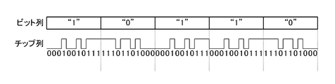
- FIG. 16 shows an example of a chip sequence generated by the transmission side device by encoding.
- “00010010111” having a length of 11 chips is used as a known code string having autocorrelation characteristics.
- the transmission bit string is “10110”.
- the code string is directly used as a transmission chip string.
- the inverted code string of the code string is a transmission chip string.
- the receiving device When the receiving device receives the transmission chip sequence transmitted by the transmitting device, the receiving device inputs each chip sequentially into a first-in first-out shift register having a capacity of 11 chips, and is temporarily stored in the shift register each time.
- the correlation value between the 11-chip chip sequence and the known code sequence is calculated. Since the code string has autocorrelation, the calculated correlation value is the maximum value (in this example, +11) when the chip string stored in the shift register is exactly “00010010111”. When the value is exactly “11101101000” (an inverted code string of a known code string), the minimum value ( ⁇ 11 in this example) is obtained. On the other hand, the correlation value in other cases is a value close to 0 (in this example, +1 or ⁇ 1).
- the reception-side device is configured to extract transmission data transmitted by the transmission-side device from the received chip sequence using such a correlation value feature.
- the communication method using the direct spreading method as described above has a problem that it is difficult to obtain a high bit rate.
- 11 chips are required to express 1 bit (binary value), so that the bit rate can only be 1/11 of the chip rate. Since it is not easy to increase the chip rate, it has become difficult to obtain a high bit rate as a result.
- one of the objects of the present invention is to provide a sensor controller, a position indicator, and a position detection system that can obtain a higher bit rate than the background art.
- a sensor controller is a sensor controller used in a position detector that detects the position of a position indicator on a touch surface, and outputs a symbol value to be transmitted to the position indicator.
- a position indicator is a position indicator configured to be able to receive a signal transmitted from a sensor controller via a position detector having a touch surface, and receives the signal and is included in the signal.
- a receiver that demodulates the value of a symbol included in the signal based on a cyclic shift amount of a code string having an autocorrelation characteristic and restores a command transmitted based on a demodulation result;
- a control unit that controls transmission of signals to the sensor controller.
- a position detection system is a position detection system including a position indicator and a position detector that detects a position of the position indicator on a touch surface, and the position detector includes the position detector.
- a control unit that outputs a value of a symbol to be transmitted to an indicator, and a code sequence having an autocorrelation characteristic is cyclically shifted by a shift amount based on at least a part of the value of the symbol to be transmitted.
- a transmission unit that transmits the generated transmission signal to the position indicator via the touch surface, and the position indicator performs the transmission.
- a series of chips generated by receiving a signal are sequentially input to a first-in first-out shift register, and each time an input is made, a sequence of chips temporarily stored in the shift register and an autocorrelation characteristic are input.
- a receiver that detects a bit string included in the series of chips by calculating a correlation value with each of a plurality of code strings obtained by cyclically shifting a predetermined code string having an arbitrary shift amount It is to have.
- a cyclic shift of a code string is used for generating a chip string, it is possible to express two or more bits with one code string. Therefore, it is possible to obtain a high bit rate at the same chip rate as compared to the background technology in which only one bit can be expressed by one code string.
- FIG. 3 is a block diagram illustrating functional blocks of a diffusion processing unit 63 illustrated in FIG. 2. It is a block diagram which shows the functional block of the control circuit 63a shown in FIG. FIG.
- the solid line in (a) shows the correlation value between the code string C1-0 shown in FIG. 8 and the code string obtained by cyclically shifting the portion of the code string C1-0 excluding the fixed chip NRa with an arbitrary shift amount.
- the broken line in (a) is a diagram showing a correlation value between the spreading code PN shown in FIG. 6 and a code string obtained by cyclically shifting the spreading code PN by an arbitrary shift amount,
- the solid line in (b) shows the correlation value between the code string C1-0 shown in FIG. 8 and the code string formed by cyclically shifting the portion of the inverted code except the fixed chip NRa with an arbitrary shift amount.
- the broken line in (b) is a diagram showing a correlation value between the spreading code PN shown in FIG. 6 and a code string formed by cyclically shifting the inverted code by an arbitrary shift amount. It is a figure which shows the example of 2nd control signal US_c2.
- FIG. 5 is a block diagram showing functional blocks of a correlation circuit 26b shown in FIG.
- FIG. 7 is an explanatory diagram of a chip row CN2 output from the shift register 63d of FIG. 6 in the first modification example of the embodiment of the present invention.
- FIG. 7 is an explanatory diagram of a chip row CN2 output from the shift register 63d of FIG. 6 in the first modification example of the embodiment of the present invention.
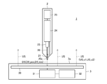
- FIG. 1 is a diagram showing a configuration of a position detection system 1 according to an embodiment of the present invention.
- the position detection system 1 includes a stylus 2 and a position detector 3.
- the stylus 2 is an active ES type position indicator configured to be able to receive signals sequentially transmitted by the position detector 3, and as shown in FIG. 1, a wick 20, an electrode 21, a pen pressure detection sensor 23, A circuit unit 24 and a power source 25 are included.
- the power source 25 for example, a cylindrical AAAA battery is used.
- the present invention can be suitably applied to a case in which a stylus of another system such as an electromagnetic induction system is used. It is.
- the core 20 is a rod-shaped member that is arranged such that its longitudinal direction coincides with the pen axis direction of the stylus 2.
- a conductive material is applied to the surface of the tip portion 20 a of the core 20 to constitute the electrode 21.
- the rear end of the lead 20 is in contact with the writing pressure detection sensor 23.
- the writing pressure detection sensor 23 is used to detect the pressure (writing pressure) applied to the tip 20 a of the core 20.
- the circuit unit 24 has a function of receiving the uplink signal US (the first control signal US_c1 and the second control signal US_c2) transmitted by the position detector 3 via the electrode 21, and the electrode toward the position detector 3. 21 and a function of transmitting a downlink signal DS (position signal DS_pos and data signal DS_res) via 21. These signals will be described in detail later.
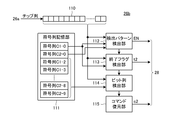
- the position detector 3 includes a sensor 30 that constitutes the touch surface 3a, a sensor controller 31, and a host processor 32 that controls each part of the position detector 3 including these.
- the sensor controller 31 receives a downlink signal DS (position signal DS_pos and data signal DS_res) transmitted from the stylus 2 via the sensor 30 and an uplink signal US (first signal via the sensor 30 toward the stylus 2). 1 control signal US_c1 and second control signal US_c2).
- FIG. 2 is a diagram showing the configuration of the position detector 3.
- the sensor 30 has a configuration in which a plurality of linear electrodes 30X and a plurality of linear electrodes 30Y are arranged in a matrix, and the stylus 2 and the capacitance are formed by these linear electrodes 30X and 30Y.
- the sensor controller 31 includes a transmission unit 60, a selection unit 40, a reception unit 50, a logic unit 70, and an MCU 80 (control unit).
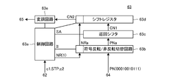
- the transmission unit 60 is a circuit for transmitting the uplink signal US (the first control signal US_c1 and the second control signal US_c2) illustrated in FIG. Specifically, it includes a first control signal supply unit 61, a switch 62, a spread processing unit 63, a code string holding unit 64, and a transmission guard unit 65.
- the first control signal supply unit 61 is described as being included in the transmission unit 60 in the present embodiment, but may be included in the MCU 80.
- the first control signal supply unit 61 holds the detection pattern c1, and according to an instruction of the control signal ctrl_t1 supplied from the logic unit 70, during a continuous transmission period TCP (for example, 3 msec) shown in FIG. It has a function of continuously and repeatedly outputting a signal (or bit string) corresponding to the detection pattern c1. Also, it has a function of outputting a predetermined delimiter pattern STP at least twice continuously immediately after the end of the continuous transmission period TCP or at the start of transmission of the second control signal US_c2.
- the first control signal US_c1 is constituted by the detection pattern c1 and the delimiter pattern STP output in this way from the first control signal supply unit 61.
- the detection pattern c1 is a pattern of symbol values used by the stylus 100 to detect the presence of the sensor controller 31.
- the detection pattern c1 is made known to the stylus 100 in advance (before the stylus 100 detects the sensor controller 31).
- a symbol is a unit of information used for modulation in transmission processing (a unit of information expressed by a transmission signal), and is a unit of information obtained by demodulating one symbol that is a reception signal in reception processing.
- the symbol value includes a value converted into a bit string (hereinafter referred to as “bit string corresponding value”) and a value not converted into a bit string by the stylus 100 that has received the symbol (hereinafter referred to as “bit string non-corresponding value”). Can be included.
- the former symbol takes the value of the power of 2 and can be associated with a bit string such as “0001”.
- the bit length of each symbol represented by the bit string is determined by the specification of the direct spreading unit 63.
- the symbol relating to the latter takes one or more (for example, two) values, and takes a value that does not correspond to a bit string such as “P” or “M” as shown in Table 1 described later.
- “P” and “M” are associated with a predetermined spreading code string and its inverted code string, respectively.
- the detection pattern c1 can be represented by a bit string non-corresponding value pattern.
- the detection pattern c1 can be configured by repeating two bit string non-corresponding values “P” and “M” like “PMPMPM. .
- the delimiter pattern STP is a symbol pattern for notifying the stylus 100 of the end of the continuous transmission period, and is configured by a symbol pattern that does not appear during the repetition of the detection pattern c1.
- the detection pattern c1 is configured by repeating two bit string non-corresponding values “P” and “M” like “PMPMPM...”
- the delimiter pattern STP is a bit string non-corresponding value. It can be constituted by a pattern “PP” in which “P” is continued twice. Note that the configuration of the separation pattern STP and the detection pattern c1 may be reversed, the separation pattern may be configured by “PM”, and the detection pattern c1 may be configured by “PP”.
- the switch 62 has a function of selecting one of the first control signal supply unit 61 and the MCU 80 based on the control signal ctrl_t2 supplied from the logic unit 70, and supplying the selected one output to the diffusion processing unit 63.
- the switch 62 selects the first control signal supply unit 61, the detection pattern c1 or the delimiter pattern STP is supplied to the diffusion processing unit 63.
- control information c2 is supplied to the diffusion processing unit 63.
- the control information c2 is information including a command indicating the instruction content to the stylus 2, is generated by the MCU 80, and is transmitted by the second control signal US_c2 as shown in FIG.
- the control information c2 includes a symbol value (for example, 0 to 15) associated with a variable-length bit string, and is different from the detection pattern c1 in that the value is not shared with the stylus 2 in advance.
- the control information c2 is indicated by a value “D” indicating the number of powers of 2 (eight values) of the predetermined bit length described above, and includes a detection pattern c1 including values “P” and “M”. Is different.
- second control signal US_c2 includes a transmission pattern (chip sequence) corresponding to three pieces of control information c2 indicated by D1 to D3 after a delimiter pattern STP “PP” as a preamble, and is transmitted.
- the code string holding unit 64 has a function of generating and holding a 11-chip long spreading code PN (second code string) having autocorrelation characteristics based on the control signal ctrl_t3 supplied from the logic unit 70.
- the spreading code PN held by the code string holding unit 64 is supplied to the spreading processing unit 63. Specific contents of the spread code PN will be described later.
- the spreading processing unit 63 sets the spreading code PN held by the code string holding unit 64 to 1 based on the value of the symbol supplied via the switch 62 (information expressed by the transmission signal by the processing of the spreading processing unit 63).
- a function chip sequence acquisition function for obtaining a code sequence of 12 chips in length (table 1 described later, chip sequence CN2 shown in FIG. 6; second chip sequence) by performing next modulation (cyclic shift or inversion described later).
- the chip array acquisition function (primary modulation processing) will be described in more detail with reference to FIGS. 5 to 9 later, but only the outline will be briefly described here.
- the detection pattern c1, the delimiter pattern STP, and the control information c2 are combinations of bit string corresponding values 0 to 15 (corresponding bit strings “0000” to “1111”) and bit string non-corresponding values “P” and “M”, respectively. Composed.
- the spreading code PN supplied from the spreading code holding unit 64 is “00010010111”.
- Table 1 shows a specific example of the correspondence between the value of the symbol by the chip sequence acquisition function and the generated chip sequence CN2.
- one symbol indicates a multi-value
- the symbol value is any one of the above-described Table 1 obtained by cyclically shifting the spread code PN by a shift amount based on the value of the symbol and performing non-inversion or inversion.
- the symbol value is one of the numbers of powers of 2 (for example, 16) represented by a bit string having a predetermined bit length (for example, “0 to 15”), or the value of the number of powers of 2 not corresponding to the bit string. Any one of one or more values (“P” and “M”) different from.
- the former is used for transmission of control information c2, and the latter is used for transmission of a delimiter pattern STP such as a preamble.
- the symbol value “P” is a bit string non-corresponding value, and is converted into a code string in which a fixed chip “1” is added to the head of a spreading code PN “00010010111” having autocorrelation characteristics.
- the bit string non-corresponding value “M” is converted into a code string in which the fixed code “0” is added to the head of the inverted code “11101101000” obtained by inverting the polarity of the spreading code PN “00010010111”.
- Each bit string corresponding value 0 to 7 is converted into a code string in which “1” is added to the head of the code formed by cyclically shifting the spread code PN by the shift amount shown in Table 1, respectively.
- the symbol value “4” is converted into a code string in which “1” is added to the head of a code formed by cyclically shifting nine spread codes PN to the right (2 to the left).
- Each of the bit string corresponding values 8 to 15 has an inverted code “11101101000” in which the polarity of the spread code PN is inverted, and “0” at the head of the code obtained by cyclically shifting each symbol value by a predetermined shift amount. It is converted into a code string.
- the symbol value “12” is converted into a code string in which “1” is added to the head of a code obtained by inverting the spread code PN and cyclically shifting the code 9 to the right (2 to the left).
- the difference in the shift amount of the closest shift amount of bit string corresponding values 0 to 7 used in the command is 1.
- the shift value (ie, 0) of the symbol value “P” used for the delimiter pattern STP such as the preamble and the closest value “0” (2 to the right) of the bit string corresponding values 0 to 7 used for the command.
- the shift amount of “4” (2 on the left) is 2, which is larger than the minimum difference among the shift amounts of the bit string corresponding values 0 to 7.
- the shift values (“0”) of the symbol values “P” and “M” constituting the delimiter pattern such as the preamble and the values (“0”, “4”, “8”, “12”) constituting the command.
- the shift amount the smaller the Hamming distance between the bit string associated with the value of one symbol and the bit string associated with the value of another symbol, the smaller the shift amount of the value of one symbol and the other. Is determined so that the difference from the shift amount of the value of one symbol is small. The reason why the shift amount is determined based on the hamming distance between the bit strings as shown in Table 1 instead of simply increasing the shift amount as the symbol value increases will be described later.
- the transmission unit 60 (the spread processing unit 63 that has acquired the chip sequence CN2) does not use the chip sequence CN2 acquired as shown in Table 1 as a transmission signal as it is, but modulates the carrier signal based on the chip sequence CN2.
- a process for generating a transmission signal (secondary modulation process) may be performed.
- the secondary modulation process is not necessarily required, the secondary modulation process may include a process of Manchester-encoding the chip sequence CN2.
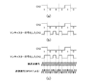
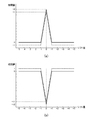
- 3 (a) to 3 (c) are diagrams showing examples of signals generated by the diffusion processing unit 63.
- FIG. Each will be described below.
- FIG. 3A shows an example in which the spread processing unit 63 does not perform the secondary modulation process.
- the chip sequence CN2 generated by the primary modulation becomes the transmission signal generated by the spread processing unit 63 as it is.
- FIG. 3B shows an example in which the spread processing unit 63 performs only Manchester encoding as the secondary modulation process.
- the diffusion processing unit 63 assigns a rising edge to a chip that is “1” among a plurality of chips included in the chip sequence CN2, and assigns a falling edge to a chip that is “0”.
- the obtained chip row CN2 is acquired.
- Manchester encoding of the chip sequence CN2 may be performed by assigning a rising edge to a chip that is “0” and assigning a falling edge to a chip that is “1”.
- the Manchester-encoded chip sequence CN2 is a transmission signal generated by the spread processing unit 63.
- FIG. 3C shows an example in which the spread processing unit 63 performs Manchester encoding and digital modulation as secondary modulation processing.
- the spread processing unit 63 modulates a predetermined carrier signal based on the Manchester-encoded chip sequence CN2, thereby generating a transmission signal as shown in FIG.
- FIG. 3 shows an example of a transmission signal generated according to BPSK (Binary Phase Shift Shift Keying), other digital modulation schemes may be used.
- BPSK Binary Phase Shift Shift Keying
- FIG. 3 shows an example of a transmission signal generated according to BPSK (Binary Phase Shift Shift Keying), other digital modulation schemes may be used.
- BPSK Binary Phase Shift Shift Keying
- FIG. 3 shows an example of a transmission signal generated according to BPSK (Binary Phase Shift Shift Keying), other digital modulation schemes may be used.
- BPSK Binary Phase Shift Shift Keying
- FIG. 3 a sine wave
- the same value does not continue over a period equal to or longer than one chip, as can be understood from FIG. 3B.
- the transmission signal whose spectrum is spread by the spreading code PN is secondarily modulated, so that it can be transmitted using a desired frequency band so as to avoid, for example, a low frequency component.
- the transmission signals (first control signal US_c1 and second control signal US_c2) generated by the spread processing unit 63 are supplied to the transmission guard unit 65.
- the transmission guard unit 65 Based on the control signal ctrl_t4 supplied from the logic unit 70, the transmission guard unit 65 transmits and receives a transmission operation between the transmission period of the first control signal US_c1 and the second control signal US_c2 and a reception period RDS described later. It has a function of inserting a guard period, which is a period during which neither transmission nor reception is performed in order to switch the operation.
- the selection unit 40 is a switch that switches between a transmission period in which a signal is transmitted from the sensor 30 and a reception period in which the signal is received by the sensor 30 based on the control of the logic unit 70. More specifically, the selection unit 40 includes switches 44x and 44y and conductor selection circuits 41x and 41y. Based on the control signal sTRx supplied from the logic unit 70, the switch 44x connects the output terminal of the transmission unit 60 to the input terminal of the conductor selection circuit 41x during the transmission period, and the conductor selection circuit 41x during the reception period. It operates to connect the output end to the input end of the receiver 50.
- the switch 44y Based on the control signal sTRy supplied from the logic unit 70, the switch 44y connects the output terminal of the transmission unit 60 to the input terminal of the conductor selection circuit 41y during the transmission period, and the conductor selection circuit 41y during the reception period. It operates to connect the output end to the input end of the receiver 50.
- the conductor selection circuit 41x operates to select one of the plurality of linear electrodes 30X based on the control signal selX supplied from the logic unit 70 and connect the selected one to the switch 44x.
- the conductor selection circuit 41y operates to select one of the plurality of linear electrodes 30Y based on the control signal selY supplied from the logic unit 70 and connect the selected one to the switch 44y.
- the receiving unit 50 is a circuit for detecting or receiving the position signal DS_pos and the data signal DS_res transmitted by the stylus 2 based on the control signal ctrl_r of the logic unit 70.
- the amplifier circuit 51 includes a detection circuit 52, a detection circuit 52, and an analog-digital (AD) converter 53.
- the amplification circuit 51 amplifies and outputs the position signal DS_pos and the data signal DS_res supplied from the selection unit 40.
- the detection circuit 52 is a circuit that generates a voltage corresponding to the level of the output signal of the amplifier circuit 51.
- the AD converter 53 is a circuit that generates a digital signal by sampling the voltage output from the detection circuit 52 at predetermined time intervals. Digital data output from the AD converter 53 is supplied to the MCU 80.
- the logic unit 70 and the MCU 80 are control units that control transmission / reception operations of the transmission unit 60, the reception unit 50, and the like.
- the MCU 80 is a microprocessor that has a ROM and a RAM therein and operates based on a predetermined program.
- the logic unit 70 is configured to output each control signal described above based on the control of the MCU 80.
- the MCU 80 is also responsible for deriving coordinate data x, y and the like indicating the position of the stylus 2 based on the digital data supplied from the AD converter 53 and outputting it to the host processor 32.
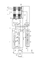
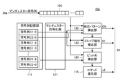
- FIG. 4 is a block diagram showing functional blocks of the stylus 2.
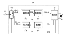
- the stylus 2 includes a switching unit SW, a receiving unit 26, a transmitting unit 27, and a control unit 28.
- the switching unit SW is a switch that switches between reception R and transmission T based on a control signal SWC from the control unit 28.
- reception R the electrode 21 is connected to the reception unit 26, and in the case of transmission T, the electrode 21 is connected to the transmission unit 27.
- the switching unit SW is set to receive R.
- the receiving unit 26 is a circuit for receiving a signal supplied from the switching unit SW (a signal arriving at the electrode 21) and obtaining a symbol value from the transmission signal shown in Table 1, and includes a demodulation circuit 26a and a correlation circuit. 26b. In order to reduce power consumption, the receiving unit 26 stops its operation except for the shortened reception period SRP in the pre-detection period BD until the sensor controller 31 is detected.
- the receiving unit 26 performs the first control only during a shortened reception period SRP (a time shorter than the period WPa, for example, 60 ⁇ sec) every predetermined period WPa (for example, 2.5 msec).
- the signal US_c1 is received, and it is determined whether or not the first control signal US_c1 includes a detection pattern c1 that is a symbol value pattern not associated with a predetermined-length bit string such as “PM” or “MP”. judge.
- the stylus 2 tries to detect the sensor controller 31 by this.
- the receiving unit 26 After detecting the sensor controller 31, the receiving unit 26 continues the receiving operation to detect the delimiter pattern STP, and further receives a signal detected after the delimiter pattern STP as the second control signal US_c2, and from there A process of extracting control information c2 composed of a value D associated with a bit string of a predetermined length is performed.
- the delimiter pattern STP is constituted by two consecutive values “PP” of the same symbol.
- the stylus 2 may receive a signal from the position detector 3 using the housing as an antenna instead of the electrode 21.
- the stylus 2 since each signal is supplied to the circuit unit 24 of the stylus 2 in a state where the sign is reversed, the stylus 2 cannot normally receive the control information c2. Therefore, when detecting the delimiter pattern STP, the stylus 2 monitors not only the symbol value “PP” but also the symbol value “MM” configured by a chip sequence obtained by inverting the chip sequence representing the symbol value “PP”. To do.
- the control information c2 is received by detecting the subsequent chip row as usual.
- the symbol value “MM” is detected, Attempts to receive the control information c2 by inverting all the chip strings after detection.
- the stylus 2 uses the casing instead of the electrode 21 by using the inversion or non-inversion of the first chip row as a reference. Even when the signal from the position detector 3 arrives and the polarity of the signal obtained at the electrode 21 has been inverted, the control information c2 is not mistakenly determined for polarity inversion and non-inversion. It becomes possible to acquire the data to constitute.
- the demodulating circuit 26a is a receiving circuit that generates a series of chips by receiving the signal transmitted by the position detector 3. More specifically, for example, if the position detector 3 performs Manchester encoding and digital modulation as the secondary modulation processing, the demodulation circuit 26a uses the spread processing unit 63 of the position detector 3 to modulate the carrier signal. A series of chips are sequentially acquired by demodulating the signal induced at the electrode 21 by the modulation method used, and further, a process of sequentially decoding the series of chips by inverse processing of Manchester encoding is performed.
- the demodulation circuit 26a is configured to supply a series of chips obtained as a result of this decoding to the correlation circuit 26b one chip at a time. When the spread processing unit 63 does not perform Manchester encoding or digital modulation, the demodulating circuit 26a may supply a series of sequentially received chips directly to the correlation circuit 26b one chip at a time.
- the correlation circuit 26b performs correlation processing between the series of chips supplied from the demodulation circuit 26a and each of a plurality of known code strings, thereby detecting the detection pattern c1, the delimiter pattern STP, and the control included in the series of chips. It has a function of detecting information c2. This detection function will be described in more detail later with reference to FIG.
- the correlation circuit 26b issues an activation signal EN to the control unit 28.
- the correlation circuit 26b outputs the detection time t2 to the control unit 28.
- the correlation circuit 26b outputs the detected control information c2 to the control unit 28.
- the control unit 28 is configured by a microprocessor (MCU), and is activated when an activation signal EN is supplied from the reception unit 26 (that is, when the reception unit 26 detects the detection pattern c1). I do. Specifically, a transmission / reception schedule of each signal (control information c2, position signal DS_pos, and data signal DS_res) is generated based on the detection time t2 supplied from the receiving unit 26, and the control signal SWC based on the generated transmission / reception schedule Is generated and supplied to the switching unit SW, and the process of controlling the transmission method of the data signal DS_res based on the control information c2 supplied from the receiving unit 26 is performed.
- MCU microprocessor
- the control of the transmission method of the data signal DS_res will be described in detail.
- the control unit 28 transmits the information to the position detector 3 according to the specification. Control the content of information. Specifically, transmission data Res including information to be transmitted is generated and supplied to the transmission unit 27.
- the transmission timing of the data signal DS_res (for example, the time slot used for transmission of the data signal DS_res) is specified by the control information c2
- the transmission unit 27 is configured to transmit the data signal DS_res at the transmission timing. The timing for supplying the transmission data Res to is controlled.
- the modulation unit 27a described later is controlled so as to generate a carrier signal of that frequency.
- the control unit 26 When the receiving unit 26 has not detected the detection pattern c1, that is, after receiving the previous activation signal EN and completing the above processing, the control unit has not yet received the next activation signal EN. 28 may pause the execution of the above processes (that is, do not execute the process of the control unit 28). Thereby, the power consumption of the control part 28 can be reduced.
- the transmission unit 27 is a circuit that transmits the position signal DS_pos and the data signal DS_res, and includes a modulation unit 27a and a booster circuit 27b.
- the modulation unit 27a generates a carrier wave signal (for example, a rectangular wave signal) having a predetermined frequency or a frequency according to the control from the control unit 28, and outputs the carrier wave signal as it is or after being modulated based on the control of the control unit 28 It is.
- the modulation unit 27a When transmitting the position signal DS_pos, the modulation unit 27a outputs the carrier signal as it is without modulating it.
- the carrier signal is modulated by the transmission data Res supplied from the control unit 28, and the transmission signal obtained as a result is output.
- PSK Phase Shift Keying
- the booster circuit 27b is a circuit that generates the position signal DS_pos and the data signal DS_res by boosting the output signal of the modulator 27a to a certain amplitude.
- the position signal DS_pos and the data signal DS_res generated by the booster circuit 27b are sent from the electrode 21 to the space via the switching unit SW.
- the booster circuit 27b and the modulation unit 27a may be realized as one processing unit.
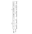
- FIG. 5 is a timing chart for explaining the operations of the stylus 2 and the sensor controller 31 in time series.
- the time axis indicated by the upper stage Ts indicates the transmission Tx and reception Rx of the stylus 2.
- the time axis indicated by the lower stage Tt indicates the transmission Tx and the reception Rx of the sensor controller 31.
- the period up to time t0 is a period in which the stylus 2 is outside the detection range of the sensor controller 31.
- the stylus 2 operates the receiving unit 26 a plurality of times intermittently with a period WPa shorter than the continuous transmission period TCP in order to reduce power consumption. Specifically, within each cycle WPa, the reception unit 26 is operated only during the shortened reception period SRP, and the reception unit 26 is stopped at other times.
- the time length of the reception period SRP is set to a value sufficient to receive the detection pattern c1 once.
- the sensor controller 31 is configured to repeat transmission of the first control signal US_c1 and the second control signal US_c2 with a period WP.
- the sensor controller 31 repeats the transmission of the chip array indicating the detection pattern c1 over a predetermined continuous transmission period TCP that is longer than the period WPa with the start of the period WP.
- the detection pattern c1 in the present embodiment is “PMPMPMP...”.
- each of the value P and the value M constituting the detection pattern c1 is converted into a chip array CN2 having a length of 12 chips by the chip array acquisition function of the diffusion processing unit 63 shown in FIG. Details will be described later.
- the sensor controller 31 transmits the chip sequence indicating the value P of the same symbol two times immediately after the end of the continuous transmission period TCP, thereby completing the transmission of the detection pattern c1 (or starting the second control signal US_c2). ) Indicating a delimiter pattern STP.
- the value P is converted into a 12-bit chip string CN2 one by one by the chip string acquisition function of the diffusion processing unit 63 shown in FIG. Thus, transmission of the first control signal US_c1 is completed.
- the sensor controller 31 that has completed the transmission of the first control signal US_c1 then transmits a chip sequence indicating the control information c2 (ie, the second control signal US_c2).
- the control information c2 is information that is transmitted subsequent to the delimiter pattern STP as described above and includes an arbitrary bit string indicating a command.
- “D1”, “D2”, “D3”,..., “Dn” shown in FIG. 4 each represents a value D that is a 4-bit arbitrary bit string (such as “0000” “0001”). 2 is converted into a chip array CN2 having a length of 12 chips by the chip array acquisition function of the diffusion processing unit 63 shown in FIG.
- the sensor controller 31 that has completed the transmission of the second control signal US_c2 provides a reception period RDS for receiving a signal from the stylus 2.
- the stylus 2 receives the first control signal US_c1 transmitted as described above, the stylus 2 is configured to transmit the position signal DS_pos within the reception period RDS.
- the sensor controller 31 waits for reception of the position signal DS_pos thus transmitted during the reception period RDS.
- the stylus 2 moves to the detection range of the sensor 30 at the time t0 (stylus down), the stylus 2 moves to the sensor controller at the timing of the time t1 immediately after the reception period SRP located in the subsequent continuous transmission period TCP.
- the detection pattern c1 transmitted by 31 is detected.
- the stylus 2 that has detected the detection pattern c1 generates the above-described activation signal EN and continues the reception operation beyond the reception period SRP thereafter.
- the sensor controller 31 transmits the delimiter pattern STP while the stylus 2 is performing this reception operation, the delimiter pattern STP is detected by the stylus 2.
- the stylus 2 detects the separation pattern STP, the stylus 2 refers to the time t2 when the detection is completed, and performs transmission / reception scheduling of the second control signal US_c2, the position signal DS_pos, and the data signal DS_res. Specifically, as shown in FIG. 5, the reception of the second control signal US_c2 is first waited at the timing based on the time t2, then the position signal DS_pos is transmitted, and finally the data signal DS_res is transmitted.
- the sensor controller 31 provides the reception period RDS after transmission of the second control signal US_c2, and waits for reception of the position signal DS_pos.
- the sensor controller 31 that has received the position signal DS_pos calculates the position (coordinate data x, y) of the stylus 2 based on the reception status of the position signal DS_pos at each of the plurality of linear electrodes 30X and 30Y shown in FIG. 1 is output to the host processor 32 shown in FIG. 1, and a reception period RDS is provided again to wait for reception of the data signal DS_res.
- the sensor controller 31 that has received the data signal DS_res extracts the transmission data Res described above from the received data signal DS_res and outputs it to the host processor 32.
- the sensor controller 31 repeats the first control signal US_c1 and the second control signal US_c2 as before. Accordingly, the stylus 2 repeats the above-described operation, and the sensor controller 31 receives the position signal DS_pos and the data signal DS_res from the stylus 2 each time, thereby calculating the position of the stylus 2 and transmitting the stylus 2 transmitted. Data Res is acquired.
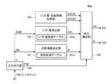
- FIG. 6 is a block diagram showing functional blocks of the diffusion processing unit 63 shown in FIG.
- the diffusion processing unit 63 includes a control circuit 63a, a sign inversion / non-inversion switching circuit 63b (code sequence generation unit), a cyclic shifter 63c (cyclic shift unit), and a shift register 63d (chip sequence generation unit). And a modulation circuit 63e.
- the code inversion / non-inversion switching circuit 63b is based on the 11-chip-length spread code PN (second code sequence) stored in the code-sequence holding unit 64, and has an 11-chip length code sequence PNa (first code) having autocorrelation characteristics. 1 code string). Specifically, according to the inversion information II supplied from the control circuit 63a, either the spreading code PN or the code string obtained by inverting the spreading code PN is selected, and the code string PNa is generated by the selected one. To do.
- the spread code PN will be described in detail.
- the spread code PN is a code string having autocorrelation characteristics. Therefore, when the correlation value between the spread code PN and the code string formed by cyclically shifting the spread code PN or its inverted signal by an arbitrary shift amount is calculated, the correlation value peak is obtained only when the shift amount is zero. Appears.
- the fact that the spreading code PN has autocorrelation characteristics will be described with reference to FIG. In the following description, it is assumed that the spreading code PN is “00010010111”.
- FIG. 9A shows the correlation value between the spread code PN “00010010111” and a code string obtained by cyclically shifting the spread code PN by an arbitrary shift amount.
- the correlation value is the correlation between the spread code PN “00010010111” and “10001001011” obtained by cyclically shifting each chip of this spread code PN one right. Value.
- the correlation value is a correlation value between the spread code PN “00010010111” and “01001011100” obtained by cyclically shifting each chip of the spread code PN to the left by two. It becomes. In the calculation of the correlation value, “0” is treated as “ ⁇ 1”.
- the broken line in FIG. 9B indicates a correlation value between a spread code PN “00010010111” and a code string obtained by cyclically shifting the inverted code “111101101000” by an arbitrary shift amount.
- the correlation value is the correlation value between the spread code PN “00010010111” and “01110110100” obtained by cyclically shifting each chip of the inverted code to the right by one. It becomes.
- the correlation value is the correlation value between the spreading code PN “00010010111” and “10110100011” obtained by cyclically shifting each chip of the inverted code to the left by two. Become.
- the peak of the correlation value indicated by the broken line appears only when the shift amount is “0”. Therefore, when the correlation value between the spread code PN and the code string formed by cyclically shifting the spread code PN or its inverted signal by an arbitrary shift amount is calculated, the peak of the correlation value is found only when the shift amount is zero. It can be said that the spreading code PN has autocorrelation characteristics.
- the sign inversion / non-inversion switching circuit 63b receives the supply of the fixed code NR from the control circuit 63a and inverts the fixed code NR in accordance with the inversion information II supplied from the control circuit 63a or does not invert the fixed chip NRa. It has the function to generate.
- the fixed code NR is a one-chip code, and is “1” in the example of FIG.
- the reason for using such a fixed code NR is to set the floor value (correlation value other than the peak) of the correlation value of the chip sequence CN2 output from the shift register 63d described later to “0”. This point will be described later in detail.
- the cyclic shifter 63c generates the chip sequence CN1 (first chip sequence) by cyclically shifting the code sequence PNa generated by the sign inversion / non-inversion switching circuit 63b by the shift amount SA supplied from the control circuit 63a. It is a functional part to do.
- the shift register 63d receives in parallel the chip sequence CN1 generated by the cyclic shifter 63c and the fixed chip NRa generated by the sign inversion / non-inversion switching circuit 63b, and adds the received fixed chip NRa to the received chip sequence CN1. This is a functional unit that generates the chip array CN2 (second chip array) and outputs the generated chip array CN2 serially.
- FIG. 8 is an explanatory diagram of the chip row CN2 output from the shift register 63d.
- the code string C1-0 shown in the figure is obtained when the sign inversion / non-inversion switching circuit 63b does not perform the inversion process and the cyclic shift by the cyclic shifter 63c is not performed (the shift amount SA is “0”).
- the chip string CN2 output from the shift register 63d is obtained by adding a fixed code NR “1” to the head of the spread code PN “00010010111”.
- the code sequence C1-n is a code sequence obtained by cyclically shifting the chip sequence CN1 portion of the code sequence C1-0 by the shift amount n, and the code inversion / non-inversion switching circuit 63b does not perform the inversion process.
- the cyclic shift is performed with the shift amount n by the cyclic shifter 63c, the chip row CN2 output from the shift register 63d is shown.
- the sign inversion / non-inversion switching circuit 63b when the sign inversion / non-inversion switching circuit 63b performs the inversion process, the cyclic shift by the cyclic shifter 63c is not performed (the shift amount SA is “0”).
- the chip sequence CN2 output from the shift register 63d is an inverted code of the code sequence C1-0.
- the code string C2-n is a code string obtained by cyclically shifting the chip string CN1 portion of the code string C2-0 by the shift amount n, and the sign inversion / non-inversion switching circuit 63b performs the inversion process. Further, the chip row CN2 output from the shift register 63d when the cyclic shift is performed with the shift amount n by the cyclic shifter 63c is shown.
- the solid line in FIG. 9A shows the code string C1-0 shown in FIG. 8 and the portion of the code string C1-0 excluding the fixed chip NRa with an arbitrary shift amount.
- the correlation value with the code string formed by cyclic shift is shown.
- the solid line in FIG. 9B arbitrarily represents a portion excluding the fixed chip NRa in the code string C1-0 shown in FIG. 8 and its inverted code (that is, the code string C2-0 shown in FIG. 8).
- the correlation value with the code string formed by cyclic shift by the shift amount is shown.
- 9A and 9B the correlation value peak indicated by the solid line appears only when the shift amount is “0”, as in the broken line example.
- the stylus 2 that receives the code sequences C1-n and C2-n stores the code sequences C1-n and C2-n in advance and calculates the correlation value with the received chip sequence to receive the received chip.
- the code sequences C1-n and C2-n included in the sequence can be detected.
- the first control signal US_c1 and the second control signal are utilized using this property. US_c2 is transmitted / received. Details of the detection operation of the code strings C1-n and C2-n by the stylus 2 will be described later.
- the floor value of the correlation value (broken line) calculated for the spread code PN is “ ⁇ 1”, whereas the correlation value calculated for the code string C1-0 ( The floor value of (solid line) is “0”.
- the floor value of the correlation value (broken line) calculated for the inverted code of the spread code PN is “+1”, whereas the calculated value is for the inverted code of the code string C1-0.
- the floor value of the correlation value (solid line) is “0”.
- the reason why the floor value of the correlation value is “0” is that the fixed chip NRa is arranged at the head of the chip row CN2, and the number of positive chips and the number of negative chips are the same. In other words, the floor value of the correlation value is set to “0” by arranging the fixed chip NRa at the head of the chip row CN2.
- the distance between the floor value “ ⁇ 1” and the maximum value “+11” of the correlation value is 10.
- the distance between the floor value “0” of the correlation value and the maximum value “+12” is 12. Therefore, it can be said that the determination error on the receiving side can be reduced by attaching the fixed chip NRa to the spread code PN and setting the floor value to “0”. Therefore, the position detector 3 according to the present embodiment can be reduced. Therefore, also from this point, it is possible to reduce the possibility of a determination error on the stylus 2 side.
- the modulation circuit 63e performs secondary modulation processing for generating a transmission signal constituting the first control signal US_c1 or the second control signal US_c2 based on the chip string CN2 generated by the shift register 63d.
- the details of the secondary modulation processing are as described above.
- the transmission signal generated by the modulation circuit 63e through the secondary modulation process reaches the sensor 30 via the transmission guard unit 65 and the selection unit 40 illustrated in FIG. 2, and is transmitted by the sensor 30 via the touch surface 3a (see FIG. 1). Is transmitted to the stylus 2.
- the control circuit 63a is a functional unit that controls the operation of each unit in the diffusion processing unit 63. As part of this function, the fixed circuit NR and the inversion information II are generated and supplied to the code inversion / non-inversion switching circuit 63b. And a function of generating a shift amount SA and supplying it to the cyclic shifter 63c.
- FIG. 7 is a block diagram showing a part related to generation of the inversion information II and the shift amount SA among the functional blocks of the control circuit 63a.
- the control circuit 63a functionally includes an input reception unit 100, an inversion information determination unit 101, a shift amount determination unit 102, a shift amount / inversion information storage unit 103, and an output selection unit 104. Composed.
- the input receiving unit 100 is a functional unit that receives input of the values P, M, and D constituting the detection pattern c1, the delimiter pattern STP, and the control information c2 from the switch 62 shown in FIG.
- the input receiving unit 100 receives an input of a value P or value M that is not associated with a specific bit string
- the input receiving unit 100 supplies the received value to the output selection unit 104.
- the most significant bit is the inverted information instruction bit IIIB (second bit string of 1 bit length to be transmitted to the stylus 2).
- the remaining amount (3 bits) as a shift amount indicating bit string SAIB (a first bit string having a predetermined bit length of 2 or more to be transmitted to the stylus 2).
- the inversion information determination unit 101 is a functional unit that determines the first inversion information II1 based on the inversion information instruction bit IIIB supplied from the input reception unit 100. Specifically, the inversion information determination unit 101 stores the inversion assignment table 101a shown in the following Table 2, and determines the first inversion information II1 according to this. The first inversion information II1 thus determined is supplied to the output selection unit 104.
- the shift amount determination unit 102 is a functional unit that determines the first shift amount SA1 based on the shift amount instruction bit string SAIB supplied from the input receiving unit 100. Specifically, the shift amount determination unit 102 stores a shift amount allocation table 102a shown in Table 3 below, and determines the first shift amount SA1 according to this. The first shift amount SA1 thus determined is supplied to the output selection unit 104.
- the shift amount determination unit 102 first determines the value “2” as the first shift amount SA1 for the bit string “000” (predetermined reference bit string).
- the value obtained by this is determined as the first shift amount SA1.
- the predetermined criterion here is that the hamming distance between the bit string before increment and the bit string after increment is 1. The meaning of adopting such a standard will be described later.
- bit string obtained by incrementing three times from the bit string “000” according to the predetermined criterion is “010”
- the shift amount / inversion information storage unit 103 stores values of the second inversion information II2, the second shift amount SA2, the third inversion information II3, and the third shift amount SA3. Specifically, “no inversion” is set as the second inversion information II2, “0” is set as the second shift amount SA2, “with inversion” is set as the third inversion information II3, and the third shift amount SA3 is set. Each “0” is stored.
- the output selection unit 104 inverts the second inversion information II2 and the second shift amount SA2 stored in the shift amount / inversion information storage unit 103 in response to the value P supplied from the input receiving unit 100.
- Information II and shift amount SA are supplied to sign inversion / non-inversion switching circuit 63b and cyclic shifter 63c shown in FIG. 6, respectively.
- the shift register 63d shown in FIG. 6 outputs the code string C1-0 shown in FIG. 8 as the chip string CN2.
- the output selection unit 104 corresponds to the supply of the value M from the input reception unit 100, and the third inversion information II3 and the third shift amount SA3 stored in the shift amount / inversion information storage unit 103.
- the shift register 63d shown in FIG. 6 outputs the code string C2-0 shown in FIG. 8 as the chip string CN2.
- the output selection unit 104 determines the inversion information in response to the fact that neither the value P nor M is supplied from the input receiving unit 100 (that is, the value D is input to the input receiving unit 100).
- the first inversion information II1 determined by the unit 101 is supplied to the sign inversion / non-inversion switching circuit 63b shown in FIG. 6 as the inversion information II, and the first shift amount SA1 determined by the shift amount determination unit 102 is shifted.
- the quantity SA is supplied to the cyclic shifter 63c shown in FIG.
- the shift register 63d shown in FIG. 6 outputs one of the code strings C1-2 to C1-9 and C2-2 to C2-9 shown in FIG. 8 as the chip string CN2.
- FIG. 8 also shows the correspondence between the 4-bit length bit string received by the input receiving unit 100 and the chip string CN2 output by the shift register 63d.
- the chip string CN2 output from the shift register 63d is the code string C1-5, that is, “110111000100”.
- the chip sequence CN2 output from the shift register 63d is the code sequence C2-5, that is, “001000111011”.
- the transmitter 60 cyclically shifts the spreading code PN having autocorrelation characteristics by a shift amount based on the value of the symbol to be transmitted, and if necessary, this It is possible to generate a transmission signal including the chip array CN2 obtained by inverting (or non-inverting). If the chip sequence CN2 can be obtained as shown in Table 1, the order of cyclic shift processing and inversion / non-inversion processing in the transmission unit 60 is not limited. Further, the transmission unit 60 stores the correspondence between the symbol values as shown in Table 1 and the chip string CN2 or a transmission signal including the symbol values in the memory, and the symbol values are stored in the memory every time the symbol values are input. The chip array CN2 may be read and transmitted.
- FIG. 10 is a diagram showing a second control signal US_c2 that the position detector 3 transmits to the stylus 2.
- the position detector 3 continuously transmits the value P constituting the delimiter pattern STP twice as a preamble, and then three values D1 “0” (0b0000) and D2 “8” as the control information c2. ”(0b1000) and D3“ 6 ”(0b0110) are transmitted.
- the code string C1-0 shown in FIG. 8, that is, “100010010111” is output as the chip string CN2 from the shift register 63d.
- the chip sequence CN2 is generated for each of the 4-bit values D1, D2, and D3.
- the code string C1-2 shown in FIG. 8, that is, “111000100101” is generated as the chip string CN2.
- the code string C2-2 shown in FIG. 8, that is, “000111011010” is generated as the chip string CN2.
- the code string C1-6 shown in FIG. 8, that is, “101011100010” is generated as the chip string CN2.
- part or all of the bit string D3 which is the last one value (4-bit value) of the control information c2 is configured by an error correction code calculated based on the bit strings D1 and D2 positioned before the bit string D3. Also good. In this way, the stylus 2 on the receiving side can detect or correct a bit error generated in the bit strings D1 and D2 by using this error correction code.
- the stylus 2 When the stylus 2 receives the chip row CN2, it may be received with the shift amount shifted by one. For example, the position detector 3 transmits the code string C1-6 shown in FIG. 8, but the stylus 2 determines that the code string is C1-7. In order to correct such erroneous determination with the above-described error correction code, it is desirable that the difference between the bit string represented by the code string C1-6 and the bit string represented by the code string C1-7 is as small as possible.
- the bit string represented by the code string C1-6 is “0110”
- the bit string represented by the code string C1-7 is “0111”
- the difference is only 1 bit. Therefore, even if an erroneous determination is made, the difference is only 1 bit, and error correction can be performed by applying an error correction code capable of 1-bit correction at the time of command transmission.
- the criterion that “the hamming distance between the bit string before incrementing and the bit string after incrementing is 1” is adopted as the predetermined criterion, and an error correction code is attached, which is robust against erroneous determination of the shift amount. A signal can be transmitted.
- FIG. 11 is a block diagram showing functional blocks of the correlation circuit 26b shown in FIG.
- the correlation circuit 26b includes a shift register 110, a code string storage unit 111, a detection pattern detection unit 112, a delimiter pattern detection unit 113 (preamble detection unit), a bit string detection unit 114, and a command restoration unit 115. It is configured.
- the shift register 110 is a first-in first-out register that accepts a series of chips acquired by the demodulation circuit 26a one by one, and is configured to be able to store chips for 12 chips. When more than 12 chips are input, the chips are deleted in order from the oldest.
- the code string storage unit 111 stores a plurality of code strings obtained by cyclically shifting a predetermined code string having autocorrelation characteristics by an arbitrary shift amount. Specifically, the code strings that need to be stored in the code string storage unit 111 are all code strings that the position detector 3 may transmit. Therefore, if the code string storage unit 111 according to the present embodiment stores the code strings C1-0, C1-2 to C1-9, C2-0, and C2-2 to C2-9 shown in FIG. Good.
- the detection pattern detection unit 112 includes a timer (not shown) therein, and outputs from the demodulation circuit 26a when the timer indicates that the current time is within the reception period SRP shown in FIG. It is a functional unit that performs the detection operation of the detection pattern c1 included in a series of chips. Specifically, each time a new chip is input to the shift register 110, this detection operation includes a chip sequence temporarily stored in the shift register 110 and a plurality of codes stored in the code sequence storage unit 111. Correlation values between the columns corresponding to the values P and M constituting the detection pattern c1, specifically the code sequence C1-0 and the code sequence C2-0 are calculated.
- the detection pattern detection unit 112 determines that the detection pattern c1 has been detected in response to continuously detecting the value P and the value M alternately a predetermined number of times, and issues the activation signal EN described above to the control unit 28. .
- the delimiter pattern detection unit 113 starts detecting the delimiter pattern STP (preamble) included in the series of chips output from the demodulation circuit 26a in response to the detection pattern detection unit 112 detecting the detection pattern c1. It is a functional part. Specifically, each time a new chip is input to the shift register 110, this detection operation includes a chip sequence temporarily stored in the shift register 110 and a plurality of codes stored in the code sequence storage unit 111. A correlation value with a value corresponding to a value P constituting the delimiter pattern STP, specifically, a code string C1-0 is calculated. Then, it is determined that the value P is detected when the calculated correlation value indicates a peak value. The delimiter pattern detection unit 113 determines that the delimiter pattern STP has been detected in response to detecting the value P twice in succession, stops the detection operation, and sets the above-described detection time t2 to the control unit 28. Output.
- the bit string detection unit 114 has a value D (4 bit length) included in a series of chips output from the demodulation circuit 26a at a timing indicated by the transmission / reception schedule generated by the control unit 28 that it is the reception period of the control information c2.
- This is a functional unit that performs a detection operation of (a bit string). Specifically, each time a new chip is input to the shift register 110, this detection operation includes a chip sequence temporarily stored in the shift register 110 and a plurality of codes stored in the code sequence storage unit 111. Correlation values with columns corresponding to the value D, specifically, code strings C1-2 to C1-9 and C2-2 to C2-9 are calculated.
- the correlation value calculated in this way indicates a peak value
- a value D (a bit string having a 4-bit length) corresponding to the code string indicating the peak value has been detected.
- the bit string detection unit 114 outputs the bit string that is the detected value D to the command restoration unit 115 each time.
- the command restoration unit 115 is a functional unit that restores the control information c2 transmitted by the position detector 3 by combining the bit strings sequentially supplied from the bit string detection unit 114.
- the command restoration unit 115 is configured to output the restored control information c2 to the control unit 28. In this way, the command transmitted by the position detector 3 is supplied to the control unit 28.
- chip row CN1 with the fixed chip NRa added to the chip row CN1 is used as the chip row CN2, it is possible to reduce the detection error on the receiving side, thereby reducing the possibility of a receiving error on the stylus 2 side. .
- a value obtained by adding the number of increments to the first shift amount SA1 determined for the reference bit string is obtained.
- the first shift amount SA1 is determined, and the criterion that “the Hamming distance between the bit string before incrementing and the bit string after incrementing is 1” is adopted as the predetermined criterion, so that the shift amount is shifted by 1 Even if the chip sequence CN2 is received, error correction due to erroneous determination of the shift amount can be suppressed to 1-bit error, and an effect that it can be realized by a shorter error correction code is obtained.
- 11 bits “00010010111” is used as the spreading code PN.
- any code string can be used as the spreading code PN as long as it has autocorrelation characteristics.
- one spread code PN is used to transmit one symbol value
- a plurality (for example, five) of the same chip sequence CN2 may be included for one symbol value. In this case, it is equivalent to transmitting the same symbol value a plurality of times (for example, five times), and the misjudgment of the shift amount can be further reduced by selecting the most probable shift amount among the plurality of shift amounts. it can.
- Tables 4 and 5 and FIGS. 12 and 13 are explanatory diagrams of the chip row CN2 output from the shift register 63d of FIG. 6 in the first modification of the above embodiment.
- This spreading code PN also has an autocorrelation characteristic like the 11-bit spreading code PN used in the above embodiment.
- the shift amount allocation table 102a is configured as shown in Table 6 below.
- This is different from the shift amount allocation table 102a shown in Table 3.
- the values of the second inversion information II2 and the second shift amount SA2 stored in the inversion allocation table 101a and the shift amount / inversion information storage unit 103 are the same as those shown in the above embodiment.
- the code string C3-0 shown in FIG. 12 corresponds to the value P
- the code string C4-0 shown in FIG. 13 corresponds to the value M
- the code strings C3-5 and C3-8 shown in FIG. C3-11, C3-14, C3-17, C3-20, C3-23, C3-26, and code strings C4-5, C4-8, C4-11, C4-14, C4 shown in FIG.
- Each of ⁇ 17, C4-20, C4-23, and C4-26 corresponds to a 4-bit long bit string.
- the code string C3-0 is obtained by adding a fixed code NR “1” to the head of the spread code PN “0000100100011011011110001010111”, and the code string C3-n corresponds to the chip string CN1 in the code string C3-0.
- the code sequence C4-0 is an inverted code of the code sequence C3-0, and the code sequence C4-n is added to the chip sequence CN1 in the code sequence C4-0. Only the corresponding part is cyclically shifted by the shift amount n.
- the shift amount is originally set to a value “1” that is +8 to the right.
- the value “0” which is originally +5 is set to the right.
- the shift amount difference of the closest ones of the shift amounts of the bit string corresponding values 0 to 7 used for the command is 3.
- the shift amount (that is, 0) of the symbol value “P” used for the delimiter pattern STP such as the preamble and the closest shift amount value “0” (5 on the right) among the bit string corresponding values 0 to 7 used in the command Alternatively, the difference from the shift amount of “4” (5 on the left) is 5, which is larger than 3 which is the difference of the shift amounts of the bit string corresponding values 0 to 7.
- the smallest difference (5) among the difference between the shift amount based on the symbol values “P” and “M” used for the delimiter pattern such as the preamble and the value constituting the command is calculated as the command.
- a delimiter pattern such as a preamble is predetermined corresponding to the command. It is possible to reduce the probability of erroneously determining that one of the values of.
- the reverse processing of Manchester encoding is performed in the demodulation circuit 26a of the stylus 2.
- the demodulation circuit 26a Even if the spread processing unit 63 of the position detector 3 performs Manchester encoding, the demodulation circuit 26a. It is good also as not performing the reverse process of Manchester encoding.
- the processing of the stylus 2 in this case will be described with reference to FIG.
- FIG. 14 is a block diagram showing functional blocks of the correlation circuit 26b according to the second modification of the above embodiment.
- the correlation circuit 26b according to this modification is replaced with the shift register 110, the detection pattern detection unit 112, the delimiter pattern detection unit 113 (preamble detection unit), and the bit string detection unit 114 shown in FIG.
- the shift register 120 includes a Manchester encoding unit 121, a detection pattern detection unit 122, a delimiter pattern detection unit 123 (preamble detection unit), and a bit string detection unit 124.
- the shift register 120 is different from the shift register 110 according to the above-described embodiment that can store only 12 chips in that it is configured to be able to store chips of 24 chips. This corresponds to the fact that the number of chips input to the shift register 120 for one chip sequence CN2 has increased to 24 because the demodulating circuit 26a does not perform the reverse process of Manchester encoding.
- the Manchester encoding unit 121 supplies the code string stored in the code string storage unit 111 to the detection pattern detection unit 122, the delimiter pattern detection unit 123, and the bit string detection unit 124, the Manchester encoding unit encodes the code string. It is a functional part. Therefore, the detection pattern detection unit 122, the delimiter pattern detection unit 123, and the bit string detection unit 124 are supplied with a Manchester encoded code string.
- the detection pattern detection unit 122, the delimiter pattern detection unit 123, and the bit string detection unit 124 include a 24-chip length chip sequence temporarily stored in the shift register 120 and a 24-chip length code in a Manchester encoded state.
- the detection pattern detection unit 112, the delimiter pattern detection unit 113, and the bit string detection unit 114 are different from each other in that the correlation value with the column is calculated. In other respects, they are the same as the detection pattern detection unit 112, the delimiter pattern detection unit 113, and the bit string detection unit 114, respectively.
- the Manchester-encoded code string usually does not show a clean autocorrelation characteristic (an autocorrelation characteristic in which all floor values are the same) as shown in FIG.
- the detection pattern detection unit 122, the division pattern detection unit 123, and the bit string detection unit 124 perform the detection pattern c1, the division pattern STP, and the 4-bit length by the above processing, respectively. It becomes possible to detect a bit string.
- the position detector 3 has been described as transmitting the second control signal US_c2 following the first control signal US_c1 as shown in FIG. 5, but the first control signal US_c1.
- the second control signal US_c2 (specifically, the chip sequence CN2 corresponding to the control information c2) ) May be transmitted.
- FIG. 15 is a timing chart for explaining the operations of the stylus 2 and the sensor controller 31 according to the third modification of the above embodiment in time series.
- the position detector 3 shown in the figure does not transmit the second control signal US_c2 following the first control signal US_c1, but after receiving the first control signal US_c1, the reception period RDS of a predetermined time length WT.
- the second control signal US_c2 is transmitted only when the position signal DS_pos is received, and is different from the position detector 3 according to the above embodiment.
- the stylus 2 considers the gap and performs the transmission and reception described above. Since the schedule can be determined, the second control signal US_c2 can be received without any problem.
- one chip column CN2 is allocated to 4 bits, but the number of bits that can be allocated to one chip column CN2 is not limited to four. In particular, when a long code string as shown in FIGS. 12 and 13 is used, a larger number of bits may be represented by one code string.
- the detection pattern c1 and the delimiter pattern STP are expressed by the dedicated code strings C1-0 and C2-0, but may be expressed by the same code string for the bit string.
- the code strings C1-0 and C2-0 are dedicated to the detection pattern c1 and the delimiter pattern STP, as shown in FIG. 8, the code string C1-0 (or code string C2-0) and the adjacent code
- the shift amount difference (2 in FIG. 8) from the columns C1-1 and C1-9 (or the code sequences C2-1 and C2-9) is expressed as the code sequence C1-n (or the code sequence C2-n) ( By making it larger than the difference in shift amount (n ⁇ 1) (1 in FIG.
- the detection errors of the detection pattern c1 and the delimiter pattern STP can be reduced, while the number of code strings that can be used for bit string transmission is reduced. End up.
- the same code string for the bit string as the delimiter pattern STP as described above an effect of increasing the number of code strings that can be used for transmitting the bit string can be obtained.
- the chip row CN1 is obtained by adding the fixed chip NRa to the chip row CN1, but the noise generated due to the fact that the floor value of the correlation value is not “0” is not a problem.
- the chip row CN1 may be used as it is as the chip row CN2.
- the chip row CN1 is obtained by adding the fixed chip NRa to the head of the chip row CN1, but the chip row CN2 is configured by adding the fixed chip NRa to the end of the chip row CN1. It is good.
- the detection pattern c1 is transmitted before the separation pattern STP.
- the stylus 2 may perform a reception operation continuously instead of intermittently, the detection pattern c1 is detected.
- the transmission of c1 may be omitted.
- the stylus 2 detects the position detector 3 by detecting the separation pattern STP.
- the present invention is applied to the signal transmitted from the position detector 3 to the stylus 2 in the above embodiment.
- the present invention is applied to the signal transmitted from the stylus 2 to the position detector 3. It is also possible to apply.
- the code processor 63b and the cyclic shifter 63c are provided in the spread processing unit 63, and the code sequence is inverted and cyclically shifted in the spread processing unit 63.
- the value of a symbol that may be input to 63a and the chip sequence CN2 to be output are stored in the storage area in association with each other, and the chip sequence CN2 corresponding to the input symbol value is stored in this storage area.
- the diffusion processing unit 63 may be configured to generate the chip row CN2 by taking out from the area.
Abstract
Description


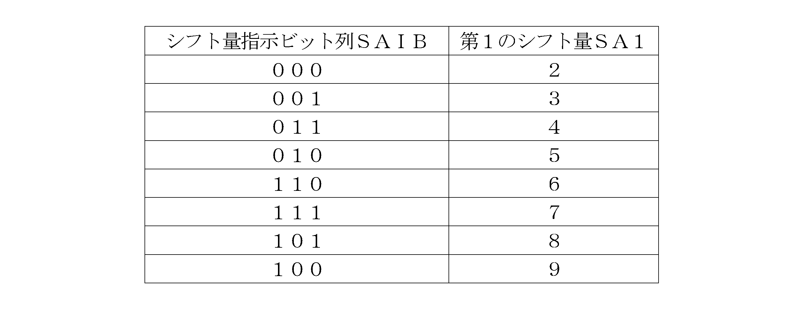

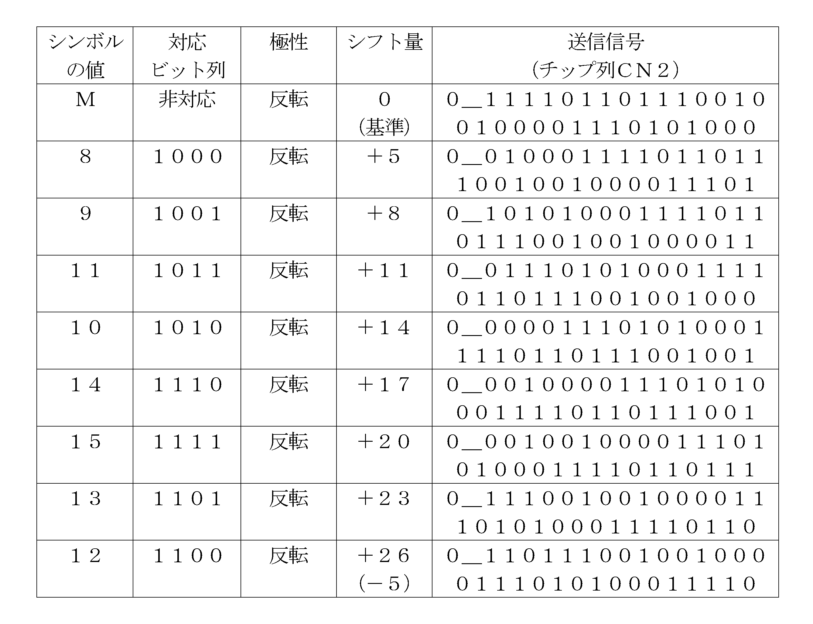
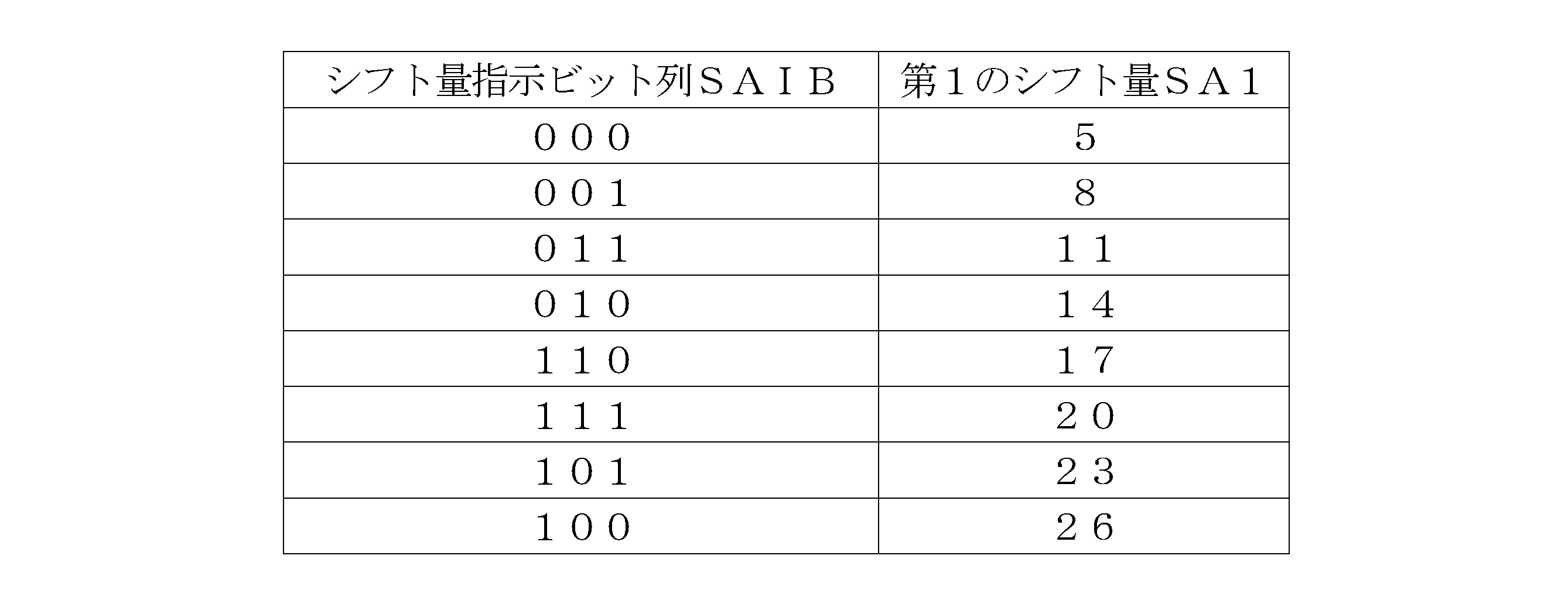
2 スタイラス
3 位置検出器
3a タッチ面
20 芯
20a 先端部
21 電極
23 筆圧検出センサ
24 回路部
25 電源
26 受信部
26a 復調回路
26b 相関回路
27 送信部
27a 変調部
27b 昇圧回路
28 制御部
30 センサ
30X,30Y 線状電極
31 センサコントローラ
32 ホストプロセッサ
40 選択部
41x,41y 導体選択回路
44x,44y スイッチ
50 受信部
51 増幅回路
52 検波回路
53 アナログデジタル変換器
60 送信部
61 制御信号供給部
62 スイッチ
63 拡散処理部
63a 制御回路
63b 符号反転/非反転切替回路
63c 巡回シフタ
63d シフトレジスタ
63e 変調回路
64 符号列保持部
65 送信ガード部
70 ロジック部
80 MCU
100 入力受付部
101 反転情報決定部
101a 反転割当テーブル
102 シフト量決定部
102a シフト量割当テーブル
103 シフト量・反転情報記憶部
104 出力選択部
110 シフトレジスタ
111 符号列記憶部
112 検出パターン検出部
113 区切パターン検出部
114 ビット列検出部
115 コマンド復元部
120 シフトレジスタ
121 マンチェスター符号化部
122 検出パターン検出部
123 区切パターン検出部
124 ビット列検出部
c1 検出パターン
c2 制御情報
CN1,CN2 チップ列
DS ダウンリンク信号
DS_pos 位置信号
DS_res データ信号
EN 起動信号
II 反転情報
II1 第1の反転情報
II2 第2の反転情報
IIIB 反転情報指示ビット
NR 固定符号
NRa 固定チップ
PN 拡散符号
PNa 符号列
SA シフト量
SA1 第1のシフト量
SA2 第2のシフト量
SAIB シフト量指示ビット列
STP 区切パターン
SW 切替部
US アップリンク信号
US_c1 第1の制御信号
US_c2 第2の制御信号 DESCRIPTION OF
100
Claims (22)
- タッチ面上における位置指示器の位置を検出する位置検出器に用いられるセンサコントローラであって、
前記位置指示器に対して送信すべきシンボルの値を出力する制御部と、
自己相関特性を有する拡散符号を、前記送信すべきシンボルの値に基づいたシフト量で巡回シフトさせて得られる第1のチップ列を含む送信信号を生成し、生成した前記送信信号を、前記タッチ面を介して前記位置指示器に対して送信する送信部と
を備えるセンサコントローラ。 A sensor controller used in a position detector that detects the position of a position indicator on a touch surface,
A control unit for outputting a value of a symbol to be transmitted to the position indicator;
A transmission signal including a first chip sequence obtained by cyclically shifting a spreading code having autocorrelation characteristics by a shift amount based on a value of the symbol to be transmitted is generated, and the generated transmission signal is converted to the touch. A sensor controller comprising: a transmission unit configured to transmit to the position indicator via a surface. - 前記シンボルは多値を示し、
前記送信信号は、前記シフト量に基づいて前記多値のいずれかの値を示す
請求項1に記載のセンサコントローラ。 The symbol is multi-valued;
The sensor controller according to claim 1, wherein the transmission signal indicates one of the multi-values based on the shift amount. - 前記シンボルは多値を示し、
前記送信部は、前記シフト量並びに前記拡散符号の非反転及び反転に基づいて前記多値のいずれかの値を示す前記送信信号を生成する、
請求項2に記載のセンサコントローラ。 The symbol is multi-valued;
The transmission unit generates the transmission signal indicating any one of the multi-values based on the shift amount and non-inversion and inversion of the spreading code;
The sensor controller according to claim 2. - 前記シンボルは、前記位置指示器への指示内容を示すコマンドを構成する2以上の所定ビット長のビット列を示す
請求項2又は3のいずれかに記載のセンサコントローラ。 The sensor controller according to claim 2, wherein the symbol indicates a bit string having a predetermined bit length of two or more that constitutes a command indicating an instruction content to the position indicator. - 前記シンボルは、所定ビット長のビット列により表される2のべき乗の個数の値のいずれか、又は、前記2のべき乗の個数の値とは異なる1個以上の個数の値のいずれかを示す
請求項2又3に記載のセンサコントローラ。 The symbol indicates either a value of the power of 2 represented by a bit string having a predetermined bit length, or one or more values different from the value of the number of power of 2. Item 4. The sensor controller according to Item 2 or 3. - 前記2のべき乗の個数の値は、前記位置指示器への指示内容を示すコマンドを構成し、
前記2のべき乗の個数の値とは異なる1個以上の個数の値は、前記コマンドの開始を示すプリアンブルを構成する
請求項5に記載のセンサコントローラ。 The value of the number of powers of 2 constitutes a command indicating the content of instructions to the position indicator,
The sensor controller according to claim 5, wherein one or more values different from the value of the power of 2 constitute a preamble indicating the start of the command. - 前記送信信号は前記シフト量並びに前記拡散符号の非反転及び反転に基づいて前記多値のいずれかの値を示す信号であって、
前記制御部は、前記コマンドを構成する前記2のべき乗の個数の値により変調された信号の非反転及び反転の判定の基準となるプリアンブルを前記コマンドより前に送信するよう制御する
請求項6に記載のセンサコントローラ。 The transmission signal is a signal indicating one of the multi-values based on the shift amount and non-inversion and inversion of the spreading code,
The control unit performs control so as to transmit a preamble that is a reference for non-inversion and inversion determination of a signal modulated by a value of the power of 2 constituting the command before the command. The described sensor controller. - 前記送信信号は、前記第1のチップ列の先端または末端に前記他の固定チップが付加された第2のチップ列を含む
請求項1に記載のセンサコントローラ。 The sensor controller according to claim 1, wherein the transmission signal includes a second chip row in which the other fixed chip is added to a front end or a terminal end of the first chip row. - 前記第2のチップ列に含まれる正のチップの数と負のチップの数は同数になる
請求項8に記載のセンサコントローラ。 The sensor controller according to claim 8, wherein the number of positive chips and the number of negative chips included in the second chip row are the same. - 前記シフト量は、ある1つのシンボルの値が対応づけられるビット列と他の1つのシンボルの値が対応付けられるビット列とのハミング距離が小さいほど、前記ある1つのシンボルの値のシフト量と前記他の1つのシンボルの値のシフト量との差が小さくなるよう構成される
請求項4に記載のセンサコントローラ。 The shift amount is such that the smaller the Hamming distance between the bit sequence associated with the value of one symbol and the bit sequence associated with the value of another symbol is, The sensor controller according to claim 4, wherein the sensor controller is configured so that a difference from a shift amount of a value of one symbol of the symbol is small. - 前記プリアンブルを構成する値に基づいた前記シフト量と前記コマンドを構成する値に基づいた前記シフト量との差のうち最も小さい値は、前記コマンドを構成するある1つの値に基づいた前記シフト量と前記コマンドを構成する他の1つの値に基づいた前記シフト量の差のうち最も小さい値よりも大きい
請求項6記載のセンサコントローラ。 The smallest value of the difference between the shift amount based on the value constituting the preamble and the shift amount based on the value constituting the command is the shift amount based on one value constituting the command. The sensor controller according to claim 6, wherein the sensor controller is larger than the smallest value among the differences in the shift amount based on the other one value constituting the command. - 前記送信部は、前記シンボルの値と前記第2のチップ列とを対応付けて記憶領域に保持しており、該記憶領域から前記送信信号を得る
請求項8又は9に記載のセンサコントローラ。 The sensor controller according to claim 8 or 9, wherein the transmission unit associates the value of the symbol with the second chip sequence and holds the value in a storage area, and obtains the transmission signal from the storage area. - タッチ面を有する位置検出器を介してセンサコントローラが送信する信号を受信可能に構成された位置指示器であって、
信号を受信し、前記信号に含まれた自己相関特性を有する符号列の巡回シフト量に基づいて前記信号に含まれたシンボルの値を復調し、復調結果に基づいて送信されたコマンドを復元する受信部と、
前記コマンドに基づいて前記センサコントローラに対する信号の送信を制御する制御部と
を含む位置指示器。 A position indicator configured to receive a signal transmitted by a sensor controller via a position detector having a touch surface,
Receiving a signal, demodulating a value of a symbol included in the signal based on a cyclic shift amount of a code string having autocorrelation characteristics included in the signal, and restoring a transmitted command based on a demodulation result A receiver,
And a control unit that controls transmission of a signal to the sensor controller based on the command. - 前記シンボルは多値を示し、前記受信部は前記シフト量に基づいて前記多値のいずれかの値を復調する
請求項13に記載の位置指示器。 The position indicator according to claim 13, wherein the symbol indicates a multi-value, and the receiving unit demodulates one of the multi-values based on the shift amount. - 前記シンボルは多値を示し、前記受信部は前記シフト量並びに前記符号列の非反転及び反転に基づいて前記多値のいずれかの値を復調する
請求項14に記載の位置指示器。 The position indicator according to claim 14, wherein the symbol indicates a multi-value, and the receiving unit demodulates one of the multi-values based on the shift amount and non-inversion and inversion of the code string. - 前記受信部は、前記シンボルの値を復調し、所定ビット長のビット列を出力する
請求項14又は15に記載の位置指示器。 The position indicator according to claim 14 or 15, wherein the reception unit demodulates the value of the symbol and outputs a bit string having a predetermined bit length. - 前記シンボルは、所定ビット長のビット列により表される2のべき乗の個数の値のいずれか、又は、前記2のべき乗の個数の値とは異なる1個以上の個数の値のいずれかを示し、
前記受信部は、
前記シンボルが前記2のべき乗の個数の値のいずれとも異なる値を示す場合に、前記コマンドの開始を示すプリアンブルを検出したことを示す信号を前記制御部に通知し、
前記シンボルが前記2のべき乗の個数の値のいずれかを示す場合に、前記シンボルに基づいて前記コマンドを復元する
請求項15又は16に記載の位置指示器。 The symbol indicates either a value of the power of 2 represented by a bit string having a predetermined bit length, or one or more values different from the value of the power of 2
The receiver is
When the symbol indicates a value different from any of the power-of-two values, the control unit is notified of a signal indicating that a preamble indicating the start of the command has been detected,
The position indicator according to claim 15 or 16, wherein the command is restored based on the symbol when the symbol indicates one of the power-of-two values. - 前記信号は前記シフト量並びに前記符号列の非反転及び反転に基づいて前記多値のいずれかの値を示す信号であって、
前記受信部は、前記コマンドより前に受信されたプリアンブルに対応する信号の非反転及び反転の別を基準として、前記符号列の非反転及び反転の有無を判定して前記シンボルを復調し、前記コマンドを復元する
請求項17に記載の位置指示器。 The signal is a signal indicating one of the multi-values based on the shift amount and non-inversion and inversion of the code string,
The receiving unit determines whether the code string is non-inverted or inverted with reference to non-inverted or inverted signal corresponding to a preamble received before the command, and demodulates the symbol, The position indicator according to claim 17, wherein the command is restored. - 前記受信部は、
前記シンボルが前記2のべき乗の個数の値のいずれかを示す場合に、前記シンボルの復調結果であるビット列を蓄積し、蓄積されて得られたビット列により誤り訂正を行う
請求項18に記載の位置指示器。 The receiver is
19. The position according to claim 18, wherein when the symbol indicates any one of the power-of-two values, a bit string that is a demodulation result of the symbol is accumulated, and error correction is performed using the accumulated bit string. Indicator. - 前記受信部は、前記信号を受信することにより生成される一連のチップを順次先入れ先出し型のシフトレジスタに入力し、入力の都度、該シフトレジスタ内に一時的に蓄積されているチップ列と、自己相関特性を有する所定の符号列を任意のシフト量で巡回シフトさせることによって得られる複数の符号列のそれぞれとの相関値を算出することにより、前記一連のチップに対応付けられたシンボルの値を復調する
請求項13に記載の位置指示器。 The receiving unit sequentially inputs a series of chips generated by receiving the signal into a first-in first-out shift register, and each time an input, a series of chips temporarily stored in the shift register By calculating a correlation value with each of a plurality of code sequences obtained by cyclically shifting a predetermined code sequence having correlation characteristics by an arbitrary shift amount, the symbol values associated with the series of chips are calculated. The position indicator according to claim 13 which demodulates. - 前記シフトレジスタ内に一時的に蓄積されているチップ列と、前記所定の符号列との相関値を算出することにより、前記一連のチップ内に含まれるプリアンブルを検出し、前記プリアンブルが検出された場合に、前記シフトレジスタ内に一時的に蓄積されているチップ列と、前記複数の符号列のそれぞれとの相関値を算出することにより、前記一連のチップ内に含まれるビット列を検出する
請求項20に記載の位置指示器。 By calculating a correlation value between a chip sequence temporarily stored in the shift register and the predetermined code sequence, a preamble included in the series of chips is detected, and the preamble is detected. In this case, a bit string included in the series of chips is detected by calculating a correlation value between a chip string temporarily stored in the shift register and each of the plurality of code strings. The position indicator according to 20. - 位置指示器と、タッチ面上における前記位置指示器の位置を検出する位置検出器とを含む位置検出システムであって、
前記位置検出器は、
前記位置指示器に対して送信すべきシンボルの値を出力する制御部と、
自己相関特性を有する符号列を、前記送信すべきシンボルの値の少なくとも一部に基づくシフト量で巡回シフトさせてなる第1のチップ列を含む送信信号を生成し、生成した前記送信信号を、前記タッチ面を介して前記位置指示器に対して送信する送信部とを有し、
前記位置指示器は、
前記送信信号を受信することにより生成される一連のチップを順次先入れ先出し型のシフトレジスタに入力し、入力の都度、該シフトレジスタ内に一時的に蓄積されているチップ列と、自己相関特性を有する所定の符号列を任意のシフト量で巡回シフトさせることによって得られる複数の符号列のそれぞれとの相関値を算出することにより、前記一連のチップ内に含まれるビット列を検出する受信部を有する
位置検出システム。 A position detection system including a position indicator and a position detector for detecting a position of the position indicator on a touch surface,
The position detector is
A control unit for outputting a value of a symbol to be transmitted to the position indicator;
A transmission signal including a first chip sequence obtained by cyclically shifting a code sequence having autocorrelation characteristics by a shift amount based on at least a part of a value of the symbol to be transmitted, and the generated transmission signal, A transmission unit for transmitting to the position indicator via the touch surface;
The position indicator is
A series of chips generated by receiving the transmission signal are sequentially input to a first-in first-out shift register, and each time it is input, it has an autocorrelation characteristic with a chip row temporarily stored in the shift register. A receiver that detects a bit string included in the series of chips by calculating a correlation value with each of a plurality of code strings obtained by cyclically shifting a predetermined code string by an arbitrary shift amount Detection system.
Priority Applications (17)
| Application Number | Priority Date | Filing Date | Title |
|---|---|---|---|
| CN201680042315.XA CN107850952B (en) | 2015-08-19 | 2016-04-19 | Sensor controller, position indicator and position detection system |
| EP20192062.6A EP3761156B1 (en) | 2015-08-19 | 2016-04-19 | Sensor controller, position indicator, and position detecting system |
| KR1020237011896A KR102619688B1 (en) | 2015-08-19 | 2016-04-19 | Sensor controller, position indicator, and position detecting system |
| KR1020237011895A KR102630271B1 (en) | 2015-08-19 | 2016-04-19 | Sensor controller, position indicator, and position detecting system |
| EP20192060.0A EP3761155B1 (en) | 2015-08-19 | 2016-04-19 | Sensor controller, position indicator, and position detecting system |
| KR1020187004654A KR102520640B1 (en) | 2015-08-19 | 2016-04-19 | Sensor controllers, position indicators, and position detection systems |
| CN202110406002.0A CN113138678B (en) | 2015-08-19 | 2016-04-19 | Method and touch control pen |
| EP22216570.6A EP4220358A3 (en) | 2015-08-19 | 2016-04-19 | Sensor controller, position indicator, and position detecting system |
| KR1020237011897A KR102623768B1 (en) | 2015-08-19 | 2016-04-19 | Sensor controller, position indicator, and position detecting system |
| EP16836828.0A EP3340018B1 (en) | 2015-08-19 | 2016-04-19 | Sensor controller, pointing device, and position detection system |
| JP2017535256A JP6235192B2 (en) | 2015-08-19 | 2016-04-19 | Sensor controller, position indicator, and position detection system |
| US15/885,442 US10452168B2 (en) | 2015-08-19 | 2018-01-31 | Sensor controller, position indicator, and position detecting system |
| US16/569,276 US10775910B2 (en) | 2015-08-19 | 2019-09-12 | Sensor controller, position indicator, and position detecting system |
| US16/659,451 US10852895B2 (en) | 2015-08-19 | 2019-10-21 | Sensor controller, position indicator, and position detecting system |
| US17/107,774 US11048366B2 (en) | 2015-08-19 | 2020-11-30 | Sensor controller, position indicator, and position detecting system |
| US17/359,993 US11556213B2 (en) | 2015-08-19 | 2021-06-28 | Sensor controller, position indicator, and position detecting system |
| US18/154,675 US20230168777A1 (en) | 2015-08-19 | 2023-01-13 | Sensor controller, position indicator, and position detecting system |
Applications Claiming Priority (4)
| Application Number | Priority Date | Filing Date | Title |
|---|---|---|---|
| US201562207257P | 2015-08-19 | 2015-08-19 | |
| US62/207257 | 2015-08-19 | ||
| JPPCT/JP2016/058254 | 2016-03-16 | ||
| PCT/JP2016/058254 WO2017029829A1 (en) | 2015-08-19 | 2016-03-16 | Method for detecting sensor controller by using stylus, stylus, and sensor controller |
Related Child Applications (2)
| Application Number | Title | Priority Date | Filing Date |
|---|---|---|---|
| US15/880,106 Continuation US10627928B2 (en) | 2015-08-19 | 2018-01-25 | Method for stylus to detect sensor controller using repeated reception of symbols, stylus, and sensor controller |
| US15/885,442 Continuation US10452168B2 (en) | 2015-08-19 | 2018-01-31 | Sensor controller, position indicator, and position detecting system |
Publications (1)
| Publication Number | Publication Date |
|---|---|
| WO2017029836A1 true WO2017029836A1 (en) | 2017-02-23 |
Family
ID=58051537
Family Applications (2)
| Application Number | Title | Priority Date | Filing Date |
|---|---|---|---|
| PCT/JP2016/058254 WO2017029829A1 (en) | 2015-08-19 | 2016-03-16 | Method for detecting sensor controller by using stylus, stylus, and sensor controller |
| PCT/JP2016/062325 WO2017029836A1 (en) | 2015-08-19 | 2016-04-19 | Sensor controller, pointing device, and position detection system |
Family Applications Before (1)
| Application Number | Title | Priority Date | Filing Date |
|---|---|---|---|
| PCT/JP2016/058254 WO2017029829A1 (en) | 2015-08-19 | 2016-03-16 | Method for detecting sensor controller by using stylus, stylus, and sensor controller |
Country Status (7)
| Country | Link |
|---|---|
| US (8) | US10627928B2 (en) |
| EP (5) | EP3340017B1 (en) |
| JP (6) | JP6745273B2 (en) |
| KR (6) | KR102496591B1 (en) |
| CN (4) | CN107850951B (en) |
| TW (1) | TWI709066B (en) |
| WO (2) | WO2017029829A1 (en) |
Cited By (6)
| Publication number | Priority date | Publication date | Assignee | Title |
|---|---|---|---|---|
| US10444870B2 (en) | 2017-11-14 | 2019-10-15 | Wacom Co., Ltd. | Sensor controller |
| WO2020230223A1 (en) * | 2019-05-10 | 2020-11-19 | 株式会社ワコム | Method for transmitting transmission data from sensor controller to pen, and pen |
| JP2021174501A (en) * | 2020-04-30 | 2021-11-01 | 深▲セン▼普贏創新科技股▲分▼有限公司 | Coordinate indicator |
| DE102021113156A1 (en) | 2020-08-18 | 2022-02-24 | Wacom Co., Ltd. | ACTIVE PEN |
| JP7341270B2 (en) | 2018-02-01 | 2023-09-08 | 株式会社ワコム | Sensor system and method for detecting a stylus |
| JP7383095B2 (en) | 2019-12-23 | 2023-11-17 | 株式会社ワコム | active pen |
Families Citing this family (21)
| Publication number | Priority date | Publication date | Assignee | Title |
|---|---|---|---|---|
| KR102346206B1 (en) | 2014-01-22 | 2022-01-03 | 가부시키가이샤 와코무 | Position indicator, position detection device, position detection circuit, and position detection method |
| CN107533386B (en) * | 2015-05-21 | 2020-12-29 | 株式会社和冠 | Active stylus |
| JP6451846B2 (en) * | 2015-06-23 | 2019-01-16 | 株式会社リコー | COMMUNICATION SYSTEM, COMMUNICATION SYSTEM CONTROL METHOD, AND PROGRAM |
| KR102523154B1 (en) * | 2016-04-22 | 2023-04-21 | 삼성전자주식회사 | Display apparatus, input device and control method thereof |
| CN109478111B (en) * | 2016-08-12 | 2022-04-12 | 株式会社和冠 | Touch control pen and sensor controller |
| KR102460472B1 (en) * | 2016-12-30 | 2022-11-01 | 엘지디스플레이 주식회사 | Touch sensing system, display device, active pen, and pen recognizing method |
| CN117348747A (en) * | 2017-02-22 | 2024-01-05 | 株式会社和冠 | Method performed by a sensor controller |
| KR102324210B1 (en) * | 2017-06-30 | 2021-11-08 | 엘지디스플레이 주식회사 | Touch display device, pen, touch system, sensing circuit, and pen recognition method |
| JP7033941B2 (en) | 2018-02-01 | 2022-03-11 | 株式会社ワコム | Sensor system |
| CN112106013B (en) * | 2018-05-09 | 2024-04-23 | 株式会社和冠 | Pen, sensor device and pen system |
| WO2020008638A1 (en) * | 2018-07-06 | 2020-01-09 | 株式会社ワコム | Active pen and sensor integrated circuit |
| KR102613842B1 (en) * | 2018-08-01 | 2023-12-13 | 주식회사 엘엑스세미콘 | Touch driving device and display driving device |
| JP2020085506A (en) * | 2018-11-16 | 2020-06-04 | アイシン精機株式会社 | Distance detector and object detector |
| JP7323336B2 (en) * | 2019-05-24 | 2023-08-08 | 株式会社ワコム | Position indicator and coordinate input device |
| EP3783463B1 (en) * | 2019-07-02 | 2022-04-13 | Shenzhen Goodix Technology Co., Ltd. | Signal processing system, chip, and active pen |
| CN110959150B (en) * | 2019-09-30 | 2023-11-07 | 深圳市汇顶科技股份有限公司 | Signal transmitting and receiving method, processor chip, active pen and touch screen |
| JP2022014973A (en) * | 2020-07-08 | 2022-01-21 | 株式会社ワコム | Method performed by stylus and sensor controller, stylus, and sensor controller |
| US20220312508A1 (en) * | 2021-03-25 | 2022-09-29 | Microsoft Technology Licensing, Llc | Electronic device pairing |
| CN114089850B (en) * | 2022-01-12 | 2022-05-10 | 深圳市千分一智能技术有限公司 | Stylus control method and device, stylus and storage medium |
| KR20230110408A (en) * | 2022-01-14 | 2023-07-24 | 삼성디스플레이 주식회사 | Display device and touch input system including the same |
| KR20230118720A (en) * | 2022-02-04 | 2023-08-14 | 삼성디스플레이 주식회사 | Display device and touch input system including the same |
Citations (2)
| Publication number | Priority date | Publication date | Assignee | Title |
|---|---|---|---|---|
| WO2015002203A1 (en) * | 2013-07-05 | 2015-01-08 | シャープ株式会社 | Touch panel system |
| JP5762659B1 (en) * | 2015-01-19 | 2015-08-12 | 株式会社ワコム | Position indicator |
Family Cites Families (39)
| Publication number | Priority date | Publication date | Assignee | Title |
|---|---|---|---|---|
| JPH05316573A (en) * | 1992-05-11 | 1993-11-26 | Alps Electric Co Ltd | Transmission and reception method for operation signal |
| US6922432B2 (en) * | 2001-03-09 | 2005-07-26 | Motorola, Inc. | System for spread spectrum communication |
| US7084860B1 (en) | 2001-06-08 | 2006-08-01 | Intertact Corporation | Method and apparatus for a touch sensitive system employing direct sequence spread spectrum (DSSS) technology |
| JP3612566B2 (en) * | 2002-05-20 | 2005-01-19 | 独立行政法人情報通信研究機構 | Code division multiplexing transmission system, transmission method, transmission device, reception device, and program |
| JP4547000B2 (en) * | 2004-04-01 | 2010-09-22 | 株式会社ワコム | Panel and cordless transducer system |
| US20080116941A1 (en) * | 2006-11-16 | 2008-05-22 | Qualcomm Incorporated | Peak signal detector |
| KR100924061B1 (en) * | 2008-03-06 | 2009-10-30 | 에스케이 텔레콤주식회사 | Channel profiler and method of profiling an incoming signal |
| US8498344B2 (en) * | 2008-06-20 | 2013-07-30 | Rambus Inc. | Frequency responsive bus coding |
| US8594250B2 (en) * | 2008-07-25 | 2013-11-26 | Qualcomm Incorporated | Apparatus and methods for computing constant amplitude zero auto-correlation sequences |
| US20100086236A1 (en) * | 2008-10-02 | 2010-04-08 | Silverbrook Research Pty Ltd | Method of imaging position-coding pattern having tag coordinates encoded by successive subsequences of cyclic position code |
| JP5430339B2 (en) * | 2009-10-19 | 2014-02-26 | 株式会社ワコム | Position detecting device and position indicator |
| JP5295090B2 (en) * | 2009-12-18 | 2013-09-18 | 株式会社ワコム | Indicator detection device |
| JP5442479B2 (en) | 2010-02-05 | 2014-03-12 | 株式会社ワコム | Indicator, position detection device and position detection method |
| WO2012057887A1 (en) | 2010-10-28 | 2012-05-03 | Cypress Semiconductor Corporation | Capacitive stylus with palm rejection |
| JP5578566B2 (en) * | 2010-12-08 | 2014-08-27 | 株式会社ワコム | Indicator detection apparatus and indicator detection method |
| GB201103822D0 (en) * | 2011-03-07 | 2011-04-20 | Isis Innovation | System for providing locality information and associated devices |
| EP2573761B1 (en) * | 2011-09-25 | 2018-02-14 | Yamaha Corporation | Displaying content in relation to music reproduction by means of information processing apparatus independent of music reproduction apparatus |
| KR20190044141A (en) * | 2011-09-30 | 2019-04-29 | 인터디지탈 패튼 홀딩스, 인크 | Device communication using a reduced channel bandwidth |
| US9946408B2 (en) | 2011-10-28 | 2018-04-17 | Atmel Corporation | Communication between a master active stylus and a slave touch-sensor device |
| US20130127744A1 (en) * | 2011-11-22 | 2013-05-23 | Qualcomm Mems Technologies, Inc. | Wireframe touch sensor design and spatially linearized touch sensor design |
| US20130257804A1 (en) * | 2012-03-29 | 2013-10-03 | Rutgers, The State University Of New Jersey | Method, apparatus, and system for capacitive touch communication |
| JP5909692B2 (en) * | 2012-04-03 | 2016-04-27 | パナソニックIpマネジメント株式会社 | Video data transmitter and receiver |
| JP6021174B2 (en) * | 2012-08-08 | 2016-11-09 | 株式会社ワコム | Position detecting device and position indicator thereof |
| JP5984259B2 (en) | 2012-09-20 | 2016-09-06 | 株式会社ワコム | Position detection device |
| KR20140046327A (en) * | 2012-10-10 | 2014-04-18 | 삼성전자주식회사 | Multi display apparatus, input pen, multi display apparatus controlling method and multi display system |
| CN102932127B (en) * | 2012-11-07 | 2015-05-06 | 哈尔滨工业大学 | Multi-base-station cooperative communication method of time division-long term evolution (TD-LTE) spread spectrum orthogonal frequency division multiplexing (OFDM) system |
| CN203164641U (en) * | 2013-01-08 | 2013-08-28 | 无锡必创传感科技有限公司 | State indicating system, state indicator and main controller |
| WO2014109138A1 (en) * | 2013-01-08 | 2014-07-17 | 株式会社村田製作所 | Spectrum spread communication apparatus |
| US9109949B2 (en) * | 2013-03-14 | 2015-08-18 | Qualcomm Mems Technologies, Inc. | Near-field optical sensing system |
| US20140267143A1 (en) * | 2013-03-15 | 2014-09-18 | Synaptics Incorporated | System and method for a transcapacitive proximity sensing device |
| WO2014185523A1 (en) * | 2013-05-17 | 2014-11-20 | シャープ株式会社 | Touch panel system and electronic device |
| KR102081108B1 (en) * | 2013-06-03 | 2020-02-25 | 엘지디스플레이 주식회사 | Detecting Touch of Input System and Touch Controller for the Same |
| US20150054783A1 (en) * | 2013-08-22 | 2015-02-26 | Microchip Technology Incorporated | Touch Screen Stylus with Communication Interface |
| CN104423750B (en) * | 2013-09-09 | 2018-09-04 | 奇景光电股份有限公司 | The touch panel and its application method of detectable stylus |
| CN104571732B (en) * | 2013-10-14 | 2018-09-21 | 深圳市汇顶科技股份有限公司 | Touch terminal, active stylus detection method and system |
| CN108279806B (en) * | 2013-11-08 | 2020-09-04 | 禾瑞亚科技股份有限公司 | Method for judging stress of transmitter, touch processing device and touch system |
| KR102346206B1 (en) | 2014-01-22 | 2022-01-03 | 가부시키가이샤 와코무 | Position indicator, position detection device, position detection circuit, and position detection method |
| JP6487694B2 (en) * | 2014-12-26 | 2019-03-20 | 株式会社ワコム | Position indicator and signal processing device |
| US10331235B2 (en) * | 2016-11-23 | 2019-06-25 | Wacom Co., Ltd. | Stylus tilt detection based on bidirectional communication between stylus and stylus sensor controller |
-
2016
- 2016-03-16 CN CN201680042094.6A patent/CN107850951B/en active Active
- 2016-03-16 KR KR1020187004653A patent/KR102496591B1/en active IP Right Grant
- 2016-03-16 WO PCT/JP2016/058254 patent/WO2017029829A1/en active Application Filing
- 2016-03-16 JP JP2017535252A patent/JP6745273B2/en active Active
- 2016-03-16 KR KR1020237003816A patent/KR102561546B1/en active IP Right Grant
- 2016-03-16 EP EP16836821.5A patent/EP3340017B1/en active Active
- 2016-04-19 EP EP22216570.6A patent/EP4220358A3/en active Pending
- 2016-04-19 EP EP16836828.0A patent/EP3340018B1/en active Active
- 2016-04-19 JP JP2017535256A patent/JP6235192B2/en active Active
- 2016-04-19 WO PCT/JP2016/062325 patent/WO2017029836A1/en active Application Filing
- 2016-04-19 KR KR1020237011897A patent/KR102623768B1/en active IP Right Grant
- 2016-04-19 EP EP20192060.0A patent/EP3761155B1/en active Active
- 2016-04-19 CN CN202110406002.0A patent/CN113138678B/en active Active
- 2016-04-19 KR KR1020237011896A patent/KR102619688B1/en active IP Right Grant
- 2016-04-19 CN CN201680042315.XA patent/CN107850952B/en active Active
- 2016-04-19 EP EP20192062.6A patent/EP3761156B1/en active Active
- 2016-04-19 CN CN202110405819.6A patent/CN113311949A/en active Pending
- 2016-04-19 KR KR1020237011895A patent/KR102630271B1/en active IP Right Grant
- 2016-04-19 KR KR1020187004654A patent/KR102520640B1/en active IP Right Grant
- 2016-07-26 TW TW105123592A patent/TWI709066B/en active
-
2017
- 2017-10-25 JP JP2017206098A patent/JP6280282B1/en active Active
-
2018
- 2018-01-18 JP JP2018006510A patent/JP6669788B2/en active Active
- 2018-01-25 US US15/880,106 patent/US10627928B2/en active Active
- 2018-01-31 US US15/885,442 patent/US10452168B2/en active Active
-
2019
- 2019-09-12 US US16/569,276 patent/US10775910B2/en active Active
- 2019-10-21 US US16/659,451 patent/US10852895B2/en active Active
-
2020
- 2020-02-27 JP JP2020031229A patent/JP6868720B2/en active Active
- 2020-04-20 US US16/853,189 patent/US10969914B2/en active Active
- 2020-08-03 JP JP2020131479A patent/JP6929999B2/en active Active
- 2020-11-30 US US17/107,774 patent/US11048366B2/en active Active
-
2021
- 2021-06-28 US US17/359,993 patent/US11556213B2/en active Active
-
2023
- 2023-01-13 US US18/154,675 patent/US20230168777A1/en active Pending
Patent Citations (2)
| Publication number | Priority date | Publication date | Assignee | Title |
|---|---|---|---|---|
| WO2015002203A1 (en) * | 2013-07-05 | 2015-01-08 | シャープ株式会社 | Touch panel system |
| JP5762659B1 (en) * | 2015-01-19 | 2015-08-12 | 株式会社ワコム | Position indicator |
Non-Patent Citations (2)
| Title |
|---|
| HIROSHI SAWAGASHIRA ET AL.: "Permutation Transmission Optical CDMA System with Cyclic- Shifted Sequences", IEICE TECHNICAL REPORT, vol. 101, no. 357, 12 October 2001 (2001-10-12), pages 23 - 29, XP009508767 * |
| See also references of EP3340018A4 * |
Cited By (11)
| Publication number | Priority date | Publication date | Assignee | Title |
|---|---|---|---|---|
| US10444870B2 (en) | 2017-11-14 | 2019-10-15 | Wacom Co., Ltd. | Sensor controller |
| DE112017007864T5 (en) | 2017-11-14 | 2020-05-28 | Wacom Co., Ltd. | Sensor control |
| US10901536B2 (en) | 2017-11-14 | 2021-01-26 | Wacom Co., Ltd. | Sensor controller |
| US11243620B2 (en) | 2017-11-14 | 2022-02-08 | Wacom Co., Ltd. | Sensor controller |
| JP7341270B2 (en) | 2018-02-01 | 2023-09-08 | 株式会社ワコム | Sensor system and method for detecting a stylus |
| WO2020230223A1 (en) * | 2019-05-10 | 2020-11-19 | 株式会社ワコム | Method for transmitting transmission data from sensor controller to pen, and pen |
| JP7383095B2 (en) | 2019-12-23 | 2023-11-17 | 株式会社ワコム | active pen |
| JP2021174501A (en) * | 2020-04-30 | 2021-11-01 | 深▲セン▼普贏創新科技股▲分▼有限公司 | Coordinate indicator |
| DE102021113156A1 (en) | 2020-08-18 | 2022-02-24 | Wacom Co., Ltd. | ACTIVE PEN |
| US11327581B2 (en) | 2020-08-18 | 2022-05-10 | Wacom Co., Ltd. | Active pen |
| US11675447B2 (en) | 2020-08-18 | 2023-06-13 | Wacom Co., Ltd. | Active pen |
Also Published As
Similar Documents
| Publication | Publication Date | Title |
|---|---|---|
| JP6280282B1 (en) | Method for performing communication between sensor controller used for position detector and position indicator, position indicator, and sensor controller | |
| US11132895B2 (en) | Method carried out in system including active stylus and sensor controller, sensor controller, and active stylus |
Legal Events
| Date | Code | Title | Description |
|---|---|---|---|
| 121 | Ep: the epo has been informed by wipo that ep was designated in this application |
Ref document number: 16836828 Country of ref document: EP Kind code of ref document: A1 |
|
| ENP | Entry into the national phase |
Ref document number: 2017535256 Country of ref document: JP Kind code of ref document: A |
|
| ENP | Entry into the national phase |
Ref document number: 20187004654 Country of ref document: KR Kind code of ref document: A |
|
| NENP | Non-entry into the national phase |
Ref country code: DE |
|
| WWE | Wipo information: entry into national phase |
Ref document number: 2016836828 Country of ref document: EP |