WO2017022162A1 - 小型アンテナ及び計算装置 - Google Patents
小型アンテナ及び計算装置 Download PDFInfo
- Publication number
- WO2017022162A1 WO2017022162A1 PCT/JP2016/002906 JP2016002906W WO2017022162A1 WO 2017022162 A1 WO2017022162 A1 WO 2017022162A1 JP 2016002906 W JP2016002906 W JP 2016002906W WO 2017022162 A1 WO2017022162 A1 WO 2017022162A1
- Authority
- WO
- WIPO (PCT)
- Prior art keywords
- resonance
- frequency
- resonance mode
- δfm
- resonance frequency
- Prior art date
- Legal status (The legal status is an assumption and is not a legal conclusion. Google has not performed a legal analysis and makes no representation as to the accuracy of the status listed.)
- Ceased
Links
Images
















Classifications
-
- H—ELECTRICITY
- H01—ELECTRIC ELEMENTS
- H01Q—ANTENNAS, i.e. RADIO AERIALS
- H01Q5/00—Arrangements for simultaneous operation of antennas on two or more different wavebands, e.g. dual-band or multi-band arrangements
- H01Q5/30—Arrangements for providing operation on different wavebands
- H01Q5/307—Individual or coupled radiating elements, each element being fed in an unspecified way
- H01Q5/342—Individual or coupled radiating elements, each element being fed in an unspecified way for different propagation modes
- H01Q5/35—Individual or coupled radiating elements, each element being fed in an unspecified way for different propagation modes using two or more simultaneously fed points
-
- H—ELECTRICITY
- H01—ELECTRIC ELEMENTS
- H01Q—ANTENNAS, i.e. RADIO AERIALS
- H01Q7/00—Loop antennas with a substantially uniform current distribution around the loop and having a directional radiation pattern in a plane perpendicular to the plane of the loop
Definitions
- the present disclosure relates to a small antenna and a calculation apparatus that can reduce the size of a modified folded dipole antenna.
- Patent Document 1 a first element that constitutes a dipole antenna with a conductor made of a line, and a second element that is arranged to face the first element with an insulator interposed therebetween and is a conductor made of a line
- a modified folded dipole antenna provided is described.
- the tip of the first element and the tip of the second element are connected, and the first element and the second element are further bent.
- a small antenna described in Patent Document 2 is known as a small antenna obtained by further downsizing the folded folded dipole antenna.
- a part of the linear portion of the element of the folded folded dipole antenna is configured to have an inductance shape (a crank shape or a shape whose width decreases toward the tip, for example, a triangle or a semi-elliptical shape). did.
- Patent Document 3 the configuration described in Patent Document 3 is known as an antenna with improved return loss of a modified folded dipole antenna.
- the return loss is improved by adjusting the impedance by adjusting the line width of the element of the modified folded dipole antenna.
- Patent Document 3 The deformed folded dipole antenna with improved return loss (see Patent Document 3) has a problem that it is difficult to reduce the size. On the other hand, even if the configuration of Patent Document 3 is applied to a miniaturized dipole antenna (see Patent Document 2) in which a part of the straight line portion has an inductance shape, it is difficult to improve the return loss satisfactorily. There's a problem.
- JP-A-2005-260567 Japanese Patent Laying-Open No. 2015-76678 JP 2011-130411 A
- This disclosure is intended to provide a small antenna and a calculation device that can be miniaturized and can improve return loss.
- the small antenna includes a pair of conductors formed of lines, and the first element whose one end of each of the pair of conductors is a feeding point, and the dielectric sandwiched therebetween.
- a second element that is disposed opposite to the first element and that is a conductor made of a line.
- a part of the line of the first element and the second element has an inductance shape of a bending structure of three or more places, or an inductance shape of a spiral structure.
- the first resonance mode in which the direction of the current flowing in the first element and the direction of the current flowing in the second element are the same has a first resonance frequency.
- the second resonance mode in which the direction of the current flowing through the first element and the direction of the current flowing through the second element are opposite has a second resonance frequency.
- the first resonance frequency of the first resonance mode is in a range from slightly above the second resonance frequency of the second resonance mode to a high anti-resonance frequency of the second resonance mode, or a little of the second resonance frequency of the second resonance mode.
- the length from the feed point to the inductance shape is set so as to fall within the range from the bottom to the antiresonance frequency having a low resonance mode.
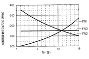
- the small antenna includes a first element including a line and a wide conductor, and a conductor including the line that is disposed to face the line portion of the first element with a dielectric interposed therebetween.
- a second element There is a feeding point at the line of the first element, the connecting portion of the wide conductor, and the end of the second element.
- a part of the line of the first element and the second element has an inductance shape of a bending structure of three or more places, or an inductance shape of a spiral structure.
- the first resonance mode in which the direction of the current flowing in the first element and the direction of the current flowing in the second element are the same has a first resonance frequency.
- the second resonance mode in which the direction of the current flowing through the first element and the direction of the current flowing through the second element are opposite has a second resonance frequency.
- the first resonance frequency of the first resonance mode is in a range from slightly above the second resonance frequency of the second resonance mode to a high anti-resonance frequency of the second resonance mode, or a little of the second resonance frequency of the second resonance mode. Further, the length from the feeding point to the inductance shape is set so as to fall within the range from the bottom to the low anti-resonance frequency of the second resonance mode.
- the calculation device for antenna design includes a first element having a pair of conductors made of lines, and one end of each of the pair of conductors being a feeding point, and a dielectric.
- a small antenna including a second element that is a conductor made of a line and is disposed opposite to the first element, with one of the lines of the first element and the second element.
- the first resonance frequency and the second resonance frequency are input, and the admittance and impedance of the small antenna are input. Calculate the reflection coefficient or return loss.
- the first resonance mode in which the direction of the current flowing in the first element and the direction of the current flowing in the second element are the same has a first resonance frequency.
- the second resonance mode in which the direction of the current flowing through the first element and the direction of the current flowing through the second element are opposite has a second resonance frequency.
- a calculation device for antenna design is arranged to face a first element composed of a line and a wide conductor and a line portion of the first element across a dielectric, A small antenna having a feeding point at the end of the first element line, a wide conductor connecting portion, and the second element.
- the first resonance frequency and the second resonance frequency are obtained for a small antenna in which part of the line of the element and the second element has an inductance shape of a bending structure at three or more locations or an inductance shape of a spiral structure.
- the first resonance mode in which the direction of the current flowing in the first element and the direction of the current flowing in the second element are the same has a first resonance frequency.
- the second resonance mode in which the direction of the current flowing through the first element and the direction of the current flowing through the second element are opposite has a second resonance frequency.
- the calculation device for antenna design includes a first element having a pair of conductors made of lines, and one end of each of the pair of conductors being a feeding point, and a dielectric.
- a small antenna including a second element that is a conductor made of a line and is disposed opposite to the first element, with one of the lines of the first element and the second element.
- a calculation device for antenna design is arranged to face a line portion of the first element with a first element composed of a line and a wide conductor and a dielectric interposed therebetween, A small antenna having a feeding point at the end of the first element line, a wide conductor connecting portion, and the second element.
- the small antenna in which part of the line of the element and the second element has an inductance shape of three or more bent structures or an inductance shape of a spiral structure, the first element and the second element The other resonance frequency of the first element and the second element or the antenna shape is calculated.
- the small antenna includes a pair of conductors formed of a line, and the first element having one end of the pair of conductors serving as a feeding point and the dielectric sandwiched between the first element and the first element. And a second element that is a conductor made of a line. Part of the lines of the first element and the second element has an inductance shape having a bending structure at three or more locations, or an inductance shape having a helical structure.
- the length from the center of the first element and the second element to the inductance shape is set so that the second resonance frequency of the second resonance mode in which the direction of the flowing current is opposite is separated.
- the line width of at least a part of the line other than the inductance shape is configured to be wider than the line width of the inductance-shaped line.
- downsizing can be achieved and return loss can be improved.
- FIG. 1A to FIG. 1D show a first embodiment of the present disclosure
- FIG. 1A shows a configuration of a modified folded dipole antenna on the first element side
- FIG. b) is a longitudinal side view of the modified folded dipole antenna
- FIG. 1C is a diagram showing a configuration of the modified folded dipole antenna on the second element side
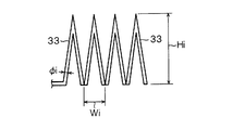
- FIG. 1D is an enlarged view of the inductance shape.
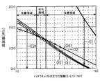
- FIG. 2 is a characteristic diagram showing the relationship between frequency and length (Lm + S).
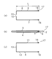
- 3 (a) to 3 (c) show a conventional configuration (part 1)
- FIG. 3 (a) shows a configuration on the first element side of the modified folded dipole antenna.
- FIG. ) Is a longitudinal side view of the modified folded dipole antenna
- FIG. 3C is a diagram showing the configuration of the second element side of the modified folded dipole antenna.
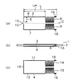
- 4 (a) to 4 (c) show a conventional configuration (No. 2).
- FIG. 4 (a) is a diagram showing a configuration of the modified folded dipole antenna on the first element side
- FIG. ) Is a vertical side view of the modified folded dipole antenna
- FIG. 4C is a diagram showing the configuration of the modified folded dipole antenna on the second element side
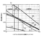
- FIG. 5 is a characteristic diagram showing the relationship between the resonance frequency and the element length.
- FIG. 6 is a characteristic diagram showing the relationship between return loss and frequency.
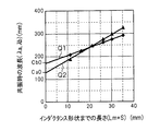
- FIG. 7 is a characteristic diagram showing the relationship between the resonance wavelength and the length (Lm + S).
- FIG. 8 is a characteristic diagram showing the relationship between return loss and frequency.
- FIG. 9 is a diagram showing an impedance chart, 10 (a) to 10 (c) show a configuration (part 1) for explaining the present disclosure, and FIG. 10 (a) shows a configuration on the first element side of the modified folded dipole antenna, FIG. 10B is a longitudinal side view of the modified folded dipole antenna, and FIG. 10C is a diagram illustrating the configuration of the modified folded dipole antenna on the second element side.
- FIG. 11 is a characteristic diagram showing the relationship between return loss and frequency.
- FIG. 12 is a characteristic diagram showing the relationship between the normalized frequency and Fa0 / Fb0.
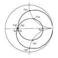
- FIG. 13 is a Smith chart of impedance Za
- FIG. 14 is a Smith chart of impedance Zb.
- FIG. 15 is a Smith chart showing the simulation result of impedance
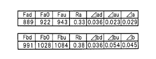
- FIG. 16 is a diagram showing each frequency and each constant as a table.
- FIG. 17 is a Smith chart that compares the simulation results with the calculation results.
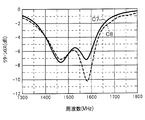
- FIG. 18 compares the simulation result with the calculation result, and is a characteristic diagram showing the relationship between the return loss and the frequency.
- FIG. 19 is a Smith chart for comparing the simulation results with the calculation results.
- FIG. 20 compares the simulation result with the calculation result, and is a characteristic diagram showing the relationship between the return loss and the frequency.
- FIG. 20 compares the simulation result with the calculation result, and is a characteristic diagram showing the relationship between the return loss and the frequency.
- FIG. 21 shows a second embodiment of the present disclosure, and is a characteristic diagram showing a relationship between a frequency and a length (Lm + S).
- 22 (a) to 22 (c) show a third embodiment of the present disclosure
- FIG. 22 (a) is a diagram showing a configuration of the modified folded monopole antenna on the first element side
- FIG. (B) is a vertical side view of the modified folded monopole antenna
- FIG. 22 (c) is a diagram showing the configuration of the modified folded monopole antenna on the second element side
- FIG. 23 is a characteristic diagram showing the relationship between frequency and length (Lm + S)
- FIG. 24 is a characteristic diagram showing the relationship between return loss and frequency
- FIG. 25 is a characteristic diagram showing the relationship between the resonance wavelength and the length (Lm + S)
- FIG. 26 is a characteristic diagram illustrating a relationship between a frequency and a length (Lm + S) according to a fourth embodiment of the present disclosure.
- 27 (a) to 27 (d) show a fifth embodiment of the present disclosure
- FIG. 27 (a) is a diagram showing a configuration of the modified folded dipole antenna on the first element side
- FIG. b) is a longitudinal side view of the modified folded dipole antenna
- FIG. 27C is a diagram showing a configuration of the modified folded dipole antenna on the second element side
- FIG. 27D is an enlarged view of the inductance shape.
- FIG. 28 is a characteristic diagram showing the relationship between return loss and frequency
- FIG. 29 is a diagram showing an impedance chart
- FIG. 30 is a characteristic diagram showing the relationship between return loss and frequency
- 31 (a) to 31 (d) illustrate a sixth embodiment of the present disclosure
- FIG. 31 (a) is a diagram illustrating a configuration of the modified folded dipole antenna on the first element side
- FIG. b) is a longitudinal side view of the modified folded dipole antenna
- FIG. 31 (c) is a diagram showing a configuration of the modified folded dipole antenna on the second element side
- FIG. 31 (d) is an enlarged view of the inductance shape.
- FIG. 32 is a characteristic diagram showing the relationship between return loss and frequency.
- 33 (a) to 33 (d) illustrate a seventh embodiment of the present disclosure.
- FIG. 33 (a) is a diagram illustrating the configuration of the modified folded dipole antenna on the first element side
- FIG. b) is a longitudinal side view of the modified folded dipole antenna
- FIG. 33 (c) is a diagram showing the configuration of the modified folded dipole antenna on the second element side
- FIG. 33 (d) is an enlarged view of the inductance shape.
- FIG. 34 is a characteristic diagram showing the relationship between return loss and frequency.
- 35 (a) to 35 (b) illustrate an eighth embodiment of the present disclosure.
- FIG. 35 (a) is a diagram illustrating the configuration of the modified folded dipole antenna on the first element side
- FIG. b) is a diagram showing a configuration on the second element side of the modified folded dipole antenna;
- FIG. 35 (a) is a diagram illustrating the configuration of the modified folded dipole antenna on the first element side
- FIG. b) is a diagram showing a configuration on the second element side of the modified folded dipole antenna;
- FIG. 35 (a) is
- FIG. 36 is an enlarged view of the inductance shape showing the ninth embodiment of the present disclosure
- FIG. 37 is an enlarged view of the inductance shape showing the tenth embodiment of the present disclosure
- FIG. 38 is an enlarged view of the inductance shape showing the eleventh embodiment of the present disclosure
- FIG. 39 is an enlarged view of the inductance shape showing the twelfth embodiment of the present disclosure
- FIG. 40 is an enlarged view of the inductance shape showing the thirteenth embodiment of the present disclosure
- FIG. 41 is an enlarged view of the inductance shape showing the fourteenth embodiment of the present disclosure
- FIG. 42 is an enlarged view of the inductance shape showing the fifteenth embodiment of the present disclosure
- FIG. 43 is an enlarged view of an inductance shape showing the sixteenth embodiment of the present disclosure
- FIG. 44 illustrates a seventeenth embodiment of the present disclosure, and is a diagram illustrating a configuration of the modified folded dipole antenna on the first element side
- FIG. 45 illustrates an eighteenth embodiment of the present disclosure, and is a diagram illustrating a configuration of a modified folded dipole antenna on the first element side
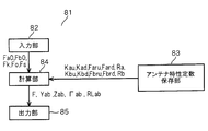
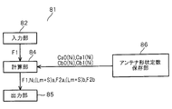
- FIG. 46 is a block diagram of a computing device showing a nineteenth embodiment of the present disclosure
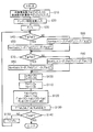
- FIG. 47 is a flowchart of calculation control
- FIG. 48 is a characteristic diagram showing the relationship between return loss and frequency.
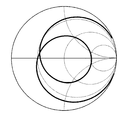
- FIG. 49 is a Smith chart.
- FIG. 50 is a block diagram of a computing device showing a twentieth embodiment of the present disclosure
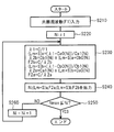
- FIG. 51 is a flowchart of calculation control
- FIG. 52 is a characteristic diagram showing the relationship between the resonance frequency and the number of semi-elliptical shapes
- FIG. 53 is a characteristic diagram showing the relationship between the length (Lm + S) and the number of semi-elliptical shapes.
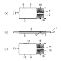
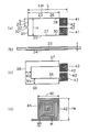
- FIG. 4 (a) to 4 (c) show a modified folded dipole antenna 1 of Patent Document 2.
- FIG. The modified folded dipole antenna 1 includes a first element 3 formed of a conductor pattern (a conductor made of a line) on one surface of a dielectric substrate 2 (see FIG. 4B), and a dielectric substrate 2.
- the second element 4 formed with a conductor pattern on the other surface of the first element 3 and the short-circuit element 5 that short-circuits the first element 3 and the second element 4 are provided.
- the first element 3 has a first L-shaped portion 6 and a second L-shaped portion 7 that are symmetric with respect to the center plane C in the antenna width direction, and these L-shaped portions.
- Inductance shapes 8 and 9 are provided at the distal ends of the long side portions 6 and 7.
- a feeding point 10 is provided at a portion of the short side portion of each of the L-shaped portions 6 and 7 that is opposed to the tip.
- the second element 4 is formed in substantially the same shape as the first element 3, and includes a pair of opposing side portions 11 and 12, and the opposing side portions 11 and 12.
- Inductive shapes 14 and 15 are provided at the other end portions of the opposing side portions 11 and 12, each having a connecting side portion 13 that connects one end.
- the short-circuit element 5 is a through-hole 16 (which connects the tip ends of the L-shaped portions 6 and 7 of the first element 3 and the tips of the other end portions of the opposing side portions 11 and 12 of the second element 4. 4 (b)).
- the inductance shapes 8 and 9 are formed in the L-shaped portions 6 and 7 of the first element 3 and the opposing side portions 11 and 12 of the second element 4, respectively.
- 14, and 15 show a modified folded dipole antenna 17 configured so as not to be provided.
- a resonance mode (referred to as resonance mode A) in which the directions of currents flowing in the first element 3 and the second element 4 are the same direction
- a resonance mode (referred to as resonance mode B) in which the direction of current flowing through the element 3 and the second element 4 is opposite.
- the lengths of the long sides of the first element 3 and the second element 4 (that is, the long sides of the L-shaped portions 6 and 7 and the long sides of the opposing sides 11 and 12) are L
- FIG. 5 shows the result of simulating changes in the resonance frequencies Fa0 and Fb0 in the resonance modes A and B when L is changed.
- the horizontal axis is L (element length)
- the vertical axis is the resonance frequency.
- a curve P ⁇ b> 1 shows a change in the resonance frequency Fa ⁇ b> 0 in the resonance mode A of the modified folded dipole antenna 17 (see FIGS. 3A to 3C), and a curve P ⁇ b> 2 represents the modified folded dipole antenna 12.
- a change in the resonance frequency Fb0 of the resonance mode B is shown.
- a curve P3 shows a change in the resonance frequency Fa0 of the resonance mode A of the modified folded dipole antenna 1 (see FIGS. 4A to 4C)
- a curve P4 shows the resonance mode of the modified folded dipole antenna 1. The change of the resonance frequency Fb0 of B is shown.
- the first change is that the resonance frequencies Fa0 and Fb0 of the two resonance modes A and B are lowered.
- the second change is that the resonance frequencies Fa0 and Fb0 of the two resonance modes A and B come close and coincide with each other.
- the modified folded dipole antenna 1 described in Patent Document 2 is made by paying attention to the effect of the first change.
- the two resonance frequencies Fa0 and Fb0 substantially coincide with each other, the two resonance modes influence each other, and the return loss increases. Therefore, the present inventor separates the two resonance frequencies Fa0 and Fb0 while changing the part of the lines of the first element 3 and the second element 4 to the inductance shapes 8, 9, 14, and 15. We tried to improve return loss by disclosing the configuration.
- the length of the short side portion of the L-shaped portion 6 of the first element 3 (and the second element 4) is S, and the L-shaped portion 6
- the length of the portion of the long side portion excluding the inductance 8 is changed, thereby separating the two wavelengths ⁇ a and ⁇ b of the two resonance modes A and B.
- the configuration in which the two resonance frequencies Fa0 and Fb0 of the two resonance modes A and B are separated from each other has been disclosed. Hereinafter, this disclosure will be specifically described.
- FIG. 6 shows a simulation of changes in return loss when the length Lm of the long side portions of the L-shaped portions 6, 7, 11, 12 is changed to, for example, 5 mm, 10 mm, 15 mm, 20 mm, 24 mm, and 29 mm. It is a figure which shows the calculated
- the horizontal axis represents frequency and the vertical axis represents return loss.
- a curve B1 shows a change in return loss when the length Lm is 5 mm.
- a curve B2 shows a change in return loss when the length Lm is 10 mm.
- a curve B3 shows a change in return loss when the length Lm is 15 mm.
- a curve B4 shows a change in return loss when the length Lm is 20 mm.
- a curve B5 shows a change in return loss when the length Lm is 24 mm.
- Curve B6 shows the change in return loss when the length Lm is 29 mm.
- FIG. 6 shows that as the first phenomenon, the length Lm is increased and the resonance frequency (that is, the frequency at which the return loss falls) is lowered. Further, as a second phenomenon, it can be seen that when the length Lm is increased, the return loss may be improved or worsened.
- the resonance frequencies Fa0 and Fb0 of the two resonance modes A and B can be calculated from the length Lm of the long sides of the L-shaped parts 6, 7, 11, and 12. And that the resonance frequency Fb0 of the resonance mode B changes depending on the presence or absence of the short-circuit element 5 connecting the first element 3 and the second element 4. This will be specifically described below.
- FIG. 7 is a diagram showing a result obtained by simulating changes in the wavelengths ⁇ a and ⁇ b of the resonance modes A and B when the lengths (Lm + S) of the first element 3 and the second element 4 are changed. is there.
- the horizontal axis is the length (Lm + S)
- the vertical axis is the wavelength at resonance.
- a straight line Q1 indicates a change in the wavelength ⁇ a of the resonance mode A
- a straight line Q2 indicates a change in the wavelength ⁇ b of the resonance mode B.
- the following relational expression is established between the two resonance frequencies Fa0 and Fb0 and the two wavelengths ⁇ a and ⁇ b at the time of resonance.
- Ca1 is the slope of the straight line Q1 (proportional constant of ⁇ a)
- Ca0 is the intercept of the straight line Q1 (constant of ⁇ a)
- Cb1 is the slope of the straight line Q2 (proportional constant of ⁇ b)
- Cb0 is the intercept of the straight line Q2 (constant of ⁇ b) ).
- the resonance frequencies Fa0 of the two resonance modes A and B are calculated from the lengths (Lm + S) of the first element 3 and the second element 4. It can be seen that Fb0 can be obtained by a calculation formula.
- the inventor is configured not to provide the short-circuit element 5 that connects the first element 3 and the second element 4 (configuration without the short-circuit element) or provides the short-circuit element 5,
- the configuration in which the resonance frequency Fb0 is changed by adjusting the position of the short-circuit element 5 and thereby the resonance frequency Fa0 and the resonance frequency Fb0 are separated (Fa0 ⁇ Fb0) is disclosed.
- FIG. 8 shows that the resonance frequency Fb0 of the resonance mode B changes depending on the presence or absence of the short-circuit element 5 in the configuration in which the length Lm of the long sides of the L-shaped portions 6, 7, 11, 12 is 15 mm, for example. This is shown in the loss graph and the impedance chart of FIG.
- FIG. 8 is a graph showing the relationship between frequency and return loss, where the horizontal axis represents frequency and the vertical axis represents return loss.
- a curve R1 shows a change in return loss of the configuration with the short-circuit element 5, that is, the modified folded dipole antenna 1 shown in FIGS. 4 (a) to 4 (c).
- a curve R2 shows a change in return loss of the configuration without the short-circuit element 5, that is, the configuration in which the short-circuit element 5 is eliminated from the modified folded dipole antenna 1 shown in FIGS. 4 (a) to 4 (c). Indicates. From FIG.
- FIG. 9 is an impedance chart.
- the curve T1 indicates the configuration with the short-circuit element 5, that is, the impedance chart of the modified folded dipole antenna 1 shown in FIGS. 4 (a) to 4 (c). Indicates.
- two curves T21 and T22 have a configuration without the short-circuit element 5, that is, a configuration in which the short-circuit element 5 is eliminated from the modified folded dipole antenna 1 shown in FIGS. 4 (a) to 4 (c).
- An impedance chart is shown. From FIG. 9, it can be seen that the resonance frequency Fa0 and the resonance frequency Fb0 substantially coincide with each other in the configuration including the short-circuit element 5. On the other hand, in the configuration without the short-circuit element 5, it can be seen that the resonance frequency Fa0 and the resonance frequency Fb0 are separated (that is, Fa0 ⁇ Fb0).
- the resonance frequency of the resonance mode B is changed by changing the position of the short-circuit element 5.
- the change of Fb0 will be described.
- the position of the short-circuit element 5 is arranged near the end of the inductance portion 8, that is, the tip of the long side portion of the L-shaped portion 6. ing.
- the position P2 of the short-circuit element 5 is set at the center (for example, eight semi-elliptical portions 16 of the inductance portion 8).
- the fourth one is arranged.
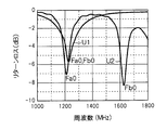
- the graph of FIG. 11 was obtained from the result of having simulated about the structure whose length Lm of the L-shaped part 6, 7, 11, 12 is 15 mm, for example.
- FIG. 11 is a graph showing the relationship between frequency and return loss, where the horizontal axis represents frequency and the vertical axis represents return loss.
- a curved line U1 shows a change in the return loss of the modified folded dipole antenna 1 shown in FIGS. 4 (a) to 4 (c) where the position of the short-circuit element 5 is the end.
- a curve U ⁇ b> 2 shows a change in the return loss of the configuration in which the position of the short-circuit element 5 is the central portion, that is, the modified folded dipole antenna 1 shown in FIGS. From FIG.
- the resonance frequency Fb0 changes, the two resonance frequencies Fa0 and Fb0 are separated (Fa0 ⁇ Fb0), and the resonance frequencies Fa0, It can be seen that the return loss of Fb0 is sufficiently small.
- the reason why the resonance frequency Fb0 of the resonance mode B changes as described above by changing the position of the short-circuit element 5 is that Cb1 (proportional constant of ⁇ b) and Cb0 ( This is because the constant of ⁇ b changes.
- the second phenomenon that is, when the length Lm is increased, the return loss may be improved or worsened, the ratio (Fa0 / Fb0) of the two resonance frequencies Fa0 and Fb0, We confirmed by paying attention to the standardized frequency at which the return loss is -6 dB or less.
- FIG. 12 is a graph showing the relationship between the ratio (Fa0 / Fb0) of the two resonance frequencies Fa0 and Fb0 and the normalized frequency at which the return loss is -6 dB or less.
- the horizontal axis represents the ratio (Fa0 / Fb0) of the two resonance frequencies Fa0 and Fb0
- the vertical axis represents the normalized frequency at which the return loss is -6 dB or less.
- the two resonance frequencies Fa0 and Fb0 the values obtained from the equations (1), (2), (3), and (4) are used, and the normalized frequency at which the return loss is ⁇ 6 dB or less.
- the value obtained from the return loss graph of FIG. 6 was used.
- the standardized frequency is Fm / Fs obtained by normalizing the frequency Fm at which the return loss is ⁇ 6 dB and the frequency Fs at which the return loss is a minimum value in the interval of ⁇ 6 dB or less. Note that when there are two frequencies Fs at which the return loss is a minimum value in a section where the return loss is ⁇ 6 dB or less as shown by the curve B5 in FIG. 6, the average value (Fs1 + Fs2) / 2 of the frequencies Fs1 and Fs2 at which the two minimum values are obtained. Is a frequency Fs at which the minimum value is obtained.
- the normalized frequency changes according to the ratio (Fa0 / Fb0) of the two resonance frequencies Fa0 and Fb0, the return loss is degraded (referred to as a degraded region), and the return loss is improved.
- It is called an improvement area).
- the ratio (Fa0 / Fb0) is 1.
- the ratio (Fa0 / Fb0) is in the range of 0.90 to 0.96 or 1.04 to 1.10. Since the return loss is degraded within the range of the degradation region, it is necessary to set the ratio (Fa0 / Fb0) of the two resonance frequencies Fa0 and Fb0 so as not to fall within this degradation region.
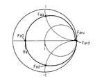
- FIG. 13 is an image diagram in which the impedance Za of the resonance mode A is plotted on the Smith chart.
- Fa0 is the resonance frequency of the resonance mode A
- the reactance value is 0, and the resistance value is Ra.
- Fard is a low antiresonance frequency of the resonance mode A, and the reactance value is ⁇ .
- the frequency value of Fard is an infinitely small frequency value.
- a value sufficiently smaller than Fa0, for example, 1 MHz is used in this embodiment in order to calculate 1 / Fard.
- Fard 1 (MHz) (7a) Faru is a high anti-resonance frequency of the resonance mode A, and the reactance value is ⁇ . The frequency value of Faru is almost twice the frequency value of Fa0.
- Ra is the resonance resistance value ( ⁇ ) of resonance mode A
- Xa is the reactance value of resonance mode A ( ⁇ ) j is an imaginary number Fard ⁇ F ⁇ Fa0, and the following three expressions hold.
- Xa Kad (1- (F / Fa0) 2 ) / (1- (F / Fard) 2 ) (11)
- Kad ((Fa0 (1 ⁇ ad) / Fard) 2 ⁇ 1) / (1 ⁇ ad) 2 )
- ⁇ ad (Fa0 ⁇ Fad) / Fa0 (13)
- F is the frequency to find the impedance Fard is the low anti-resonance frequency of resonance mode A
- reactance - ⁇ Fa0 is the resonance frequency (MHz) of resonance mode A
- the reactance is 0 Fad is the frequency at which the reactance of the resonance mode A becomes ⁇ 1.
- Kad is the proportional constant below the resonance mode A.
- ⁇ ad is the frequency ratio at which the reactance of the resonance mode A changes from ⁇ 1 to 0.
- Fa0 ⁇ F ⁇ Faru The following three expressions hold.
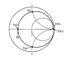
- Fb0 is the resonance frequency of the resonance mode B
- the reactance value is 0, and the resistance value is Rb.
- Fbrd is a low antiresonance frequency of the resonance mode B, and the reactance value is ⁇ .
- the frequency value of Fbrd is substantially Fb0 / 2 in the case of the configuration with the short-circuit element 5 shown in FIGS. 4A to 4C, and is an infinitesimal frequency value in the case of the configuration without the short-circuit element 5.
- a value sufficiently smaller than Fb0 for example, 1 MHz is used in this embodiment.
- Fbrd Fb0 / 2
- Fbrd 1 (MHz)
- Fbrd 2Fb03 / 3
- Fbru is a high antiresonance frequency of the resonance mode B, and the reactance value is ⁇ .
- the frequency value of Fbru is approximately 3Fb0 / 2 in the case of the configuration with the short-circuit element 5 shown in FIGS. 4A to 4C, and is approximately 2Fb0 in the case of the configuration without the short-circuit element 5. Value.
- FIG. 14 shows that the impedance Zb of the resonance mode B can be calculated by the following equation.
- Xb Kbu (1- (F / Fb0) 2 ) / (1- (F / Fbru) 2 ) (21)
- Kbu (1- (Fb0 (1 + ⁇ bu) / Fbru) 2 ) / (1- (1 + ⁇ bu) 2 )
- ⁇ bu (Fbu ⁇ Fb0) / Fb0 (23)
- F is the frequency to find the impedance
- Fbru is the high anti-resonance frequency of resonance mode B
- reactance ⁇ Fbu is the frequency at which the reactance of the resonance mode B becomes 1.
- Kbu is the proportional constant above the resonance mode B.
- ⁇ bu is the frequency ratio at which the reactance of the resonance mode B changes from 0 to 1.
- the admittances Ya and Yb of the resonance modes A and B Can be calculated by the following equation.
- Kau (1 ⁇ (Fa0 / Faru) 2 ) / 2 / ( ⁇ ⁇ a) (33)
- ⁇ bd and ⁇ bu have substantially the same value in principle, the average value ⁇ b is calculated and used as in the following equation.
- Kbd ((Fb0 (1- ⁇ b) / Fbrd) 2 ⁇ 1) / (1- (1- ⁇ b) 2 ) (35)
- Kbu (1 ⁇ (Fa0 (1 + ⁇ b) / Fbru) 2 ) / (1 ⁇ (1 + ⁇ b) 2 ) (36)
- Kbu (1 ⁇ (Fb0 / Fbru) 2 ) / 2 / ( ⁇ ⁇ b) (38)
- FIG. 15 shows the impedance simulation results together with the points of each frequency in the antenna shown in FIGS.
- FIG. 16 is a table showing the values obtained from the simulation results and the resonance resistance values, and the calculation results of the constants ⁇ a and ⁇ b calculated by the above formula.
- FIGS. 17 and 18 show the simulation results of impedance and return loss in the antenna shown in FIGS. 4A to 4C in which the parameter S is set to 6.2 mm and the parameter Lm is set to 29 mm. It is the figure which compared with the calculation result which computed the impedance and the return loss by Formula (27), (28).
- the resonance frequency (Fa 0, Fb 0) and the anti-resonance frequency (Fard, Faru, Fbrd, Fbru) are calculated.
- Each value of the resonance frequency (Fa0, Fb0) is obtained using equations (5) and (6).
- the respective values of the anti-resonance frequencies (Fard F, Faru, Fbrd, Fbru) are obtained using equations (7a), (7b), (8a), and (8b).
- FIG. 18 is a characteristic diagram showing the relationship between frequency and return loss.
- the solid line C3 shows the calculation result
- the broken line C4 shows the simulation result.
- FIGS. 19 and 20 show simulation results of impedance and return loss, and calculation results of calculating impedance and return loss according to equations (27) and (28) in a configuration in which the parameter Lm is changed from 29 mm to 5 mm.
- FIG. 20 is a characteristic diagram showing the relationship between the frequency and the return loss.
- a solid line C7 indicates a calculation result
- a broken line C8 indicates a simulation result.
- RaRb RaRb (Ra 2 + Xa 2) / (Rb 2 + Xb 2)> Xa 2 (46)
- RaRb RaRb (Ra 2 + Xa 2) / Xa 2> (Rb 2 + Xb 2)
- RaRb RaRb (Rb 2 + Xb 2) / Xb 2> (Ra 2 + Xa 2) (48) It becomes.
- Equation (53) (Fb0 ⁇ Fa0) / (Fa0 + Fb0) (54) Substituting Equation (53) into Equation (52) and ⁇ f ⁇ 1 in the range of the degradation region, RaRb>
- ⁇ fm is the frequency ratio of the degradation range boundary, and the following equation is established.
- the relationship between the two resonance frequencies Fa0 and Fb0 is such that the expressions (65), (66), (67), and (68) are satisfied, so that the expressions (3), (4), The length (Lm + S) to the inductance shape of the first element 3 or the second element 4 is adjusted using the expressions (5) and (6). Thereby, a return loss can be improved.
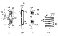
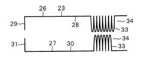
- the modified folded dipole antenna 21 of the present embodiment has a structure shown in FIGS. 1 (a) to 1 (d).
- the modified folded dipole antenna 21 includes a first element 23 formed of a conductor pattern (that is, a conductor made of a line) on one surface of a flat substrate 22 made of a dielectric (see FIG. 1B).
- the second element 24 formed of a conductor pattern (that is, a conductor made of a line) and the first element 23 and the short-circuit element 70 for short-circuiting the second element 24 are provided on the other surface of the substrate 2.
- the substrate 22 is a substrate made of a dielectric material, for example, glass epoxy. Note that the thickness of the substrate 22 (dielectric) is t, the relative dielectric constant of the substrate 22 (dielectric) is ⁇ , and the dielectric loss of the substrate 22 (dielectric) is tan ⁇ .
- the first element 23 includes a power feeding side parallel portion 25 formed of a conductor pattern (for example, a copper foil pattern).
- the feeding-side parallel portion 25 includes two L-shaped portions that are symmetrical with respect to the antenna width direction center plane (hereinafter referred to as the width direction center plane) C, that is, the first L-shaped portion 26 and the second L-shaped portion 27.
- the first L-shaped portion 26 includes a long side portion 28 and a short side portion 29.
- the long side portion 28 is parallel to the center plane C in the width direction.
- the short side portion 29 is shorter than the long side portion 28, and is connected to one end portion (the left end portion in FIG. 1A to FIG. 1D) of the long side portion 28, and is perpendicular to the long side portion 28 in the width direction. Projects in the direction of the center plane C.
- the second L-shaped portion 27 has the same configuration as the first L-shaped portion 26 and includes a long side portion 30 and a short side portion 31.
- the long side portion 30 has the same length and width as the long side portion 28 of the first L-shaped portion 26, and faces the long side portion 28 across the width direction center plane C.
- the short side portion 31 is shorter than the long side portion 30 and is connected to one end portion of the long side portion 30 (the left end portion in FIG. 1A to FIG. 1D). Further, the short side portion 31 protrudes perpendicularly from the long side portion 30 in the width direction central plane C direction.
- the width and length of the short side portion 31 are the same as the short side portion 29 of the first L-shaped portion 26.
- first L-shaped portion 26 and the second L-shaped portion 27 have the same shape, and are arranged so that the short side portions 29 and 31 face each other. And the front-end
- the above-mentioned center plane C in the width direction is a plane perpendicular to the surface of the substrate 22 and parallel to the long side portion 28 of the first L-shaped portion 26 and the long side portion 30 of the second L-shaped portion 27.
- first L-shaped portion 26 and the second L-shaped portion 27 are formed with inwardly protruding portions 33 and 33 at a part thereof.
- the inner projecting portion 33 extends in the inner direction surrounded by the first L-shaped portion 26 and the second L-shaped portion 27 in the plane of the substrate 22, and the long side portions 28 and 30 of the first L-shaped portion 26 and the second L-shaped portion 27. It protrudes from the straight part.
- the inner protrusion 33 forms an inductance shape 34.
- the term “continuous” means that the end of one inner protrusion 33 and the end of another inner protrusion 33 adjacent to the inner protrusion 33 are common. It means that Moreover, in this embodiment, the position of the both ends of the inner side protrusion part 33 exists in the same position as the lower end part (or upper end part) of the long side parts 28 and 30.
- FIG. The inner projecting portion 33 is bent from the straight portion (conductor pattern) of the long side portions 28 and 30 at one of the one (left) ends, protrudes inward, is folded back at the tip portion, and the other (right) end.
- the long side portions 28 and 30 are connected to the straight portions (conductor patterns) again.
- the width of the base portion of the inner protrusion 33 is Wi
- the height is Hi
- the line width is ⁇ i.
- the number of formed inner protrusions 33 for one inductance shape 34 is Ni.
- the first element 23 having such a configuration has a length in the longitudinal direction (element length) of the long side portions 28 and 30 as L and a length in the longitudinal direction of the long side portions 28 and 30.
- the length of the portion excluding the inductance shape 34 is Lm.
- H be the distance (element height) at which the long side portions 28 and 30 face each other.
- the line widths of the long side portions 28 and 30 are the same as the line width of the inward protruding portion 33, and are assumed to be ⁇ i.
- the length of the short sides 29 and 31 is S.
- the line widths of the short side portions 29 and 31 are the same as the line widths of the long side portions 28 and 30 (that is, the line width of the inner protruding portion 33), and are assumed to be ⁇ i.
- the second element 24 includes a non-feeding side parallel portion 35 formed of a conductor pattern (for example, a copper foil pattern).
- the non-feeding side parallel portion 35 includes a pair of opposed side portions 36 and 37 arranged to face each other, and a connecting side portion 38 that connects one ends of the pair of opposed side portions 36 and 37 to each other.
- the opposing side portions 36 and 37 are parallel to each other, and have the same length and width.
- the opposing side portion 36 has the length L (element length) described above, and faces the long side portion 28 of the first L-shaped portion 26 of the first element 23 via the substrate 22.
- the length of the other opposing side portion 37 is L.
- the facing side portion 37 faces the long side portion 30 of the second L-shaped portion 27 of the first element 23 through the substrate 22.
- the line widths of the opposing side portions 36 and 37 are the same as the line widths of the long side portions 28 and 30 of the first element 23 and are ⁇ i.
- the connecting side portion 38 is perpendicular to the two opposing side portions 36 and 37, the length (element height) is H, the line width is the same as the line width of the opposing side portions 36 and 37, and ⁇ i It is.
- the connecting side portion 38 faces the short side portion 29 of the first L-shaped portion 26 of the first element 23 and the short side portion 31 of the second L-shaped portion 26 with the substrate 22 interposed therebetween.
- inner protruding portions 39 and 39 protruding in the inner direction surrounded by the opposite side portions 36 and 37 and the connecting side portion 38 are formed.
- This inner protrusion 39 constitutes an inductance shape 40.
- the inner protruding portion 39 has the same shape as the inner protruding portion 33 formed in the first element 23, and the inner protruding portion 39 is also semi-elliptical. Further, the inner protruding portion 39 has the same size as the inner protruding portion 33. Furthermore, the number of the inner protrusions 39 is the same as that of the inner protrusions 33. In the present embodiment, 8 * 2 pieces are formed, and are formed at positions facing the inner protrusions 33, respectively.
- the short-circuit element 70 is a through-hole that connects the tip ends of the L-shaped portions 26 and 27 of the first element 23 and the tips of the other end portions of the opposing side portions 36 and 37 of the second element 24. 71 (see FIG. 1B).
- the length S of the short side portions 29 and 31 is set to, for example, 6.2 mm, and the inductance shapes 34 and 40 are excluded from the longitudinal lengths of the long side portions 28, 30, 36, and 37.
- the length Lm of the part was set to 5, 10, 15, 20, 24, or 29 mm, for example.
- the length (Lm + S) was set to 11.2, 16.2, 21.2, 26.2, 30.2, or 35.2 mm.
- Lm is 5 mm
- the short side portions 29 and 31 are longer than the long side portions 28 and 30.
- All the line widths ⁇ i are, for example, 0.2 mm
- the height Hi of the inner protrusions 33, 39 is, for example, 6 mm
- the width Wi of the base is, for example, 0.6 mm
- the thickness t of the dielectric substrate 22 is 0.8 mm. It was.
- the relative dielectric constant ⁇ of the substrate 22 was 4.9
- the dielectric loss tan ⁇ of the dielectric was 0.025.
- the antenna having improved return loss has a length (Lm + S) of 11.2, 16.2, 26.2, 30. 2, 35.2 mm.
- the antenna having a deteriorated return loss has a length (Lm + S) of 21.1 mm as shown in FIG. 6 or FIG.
- FIG. 2 is a graph showing the relationship between the length (Lm + S) and the frequency, and the improvement area and the deterioration area of the return loss will be described based on FIG.
- the horizontal axis in FIG. 2 is the length (Lm + S), and the vertical axis is the frequency.
- the curve D1 indicates the resonance frequency Fa0 of the resonance mode A
- the curve D2 indicates the resonance frequency Fb0 of the resonance mode B.
- the resonance mode A is the resonance mode in which the direction of the current flowing in the first element 23 and the second element 24 is the same direction
- the resonance mode B is the resonance mode in which the current direction is opposite.
- a curve D3 indicates a low antiresonance frequency Fbrd of the resonance mode B
- a curve D4 indicates a high antiresonance frequency Fbru of the resonance mode B.
- a curve D5 represents Fb0 ((1- ⁇ fm) / (1 + ⁇ fm)
- a curve D6 represents Fb0 ((1 + ⁇ fm) / (1- ⁇ fm)).
- These Fb0 ((1 ⁇ fm) / (1 + ⁇ fm)) and Fb0 ((1 + ⁇ fm) / (1 ⁇ fm)) are obtained from the equations (65) and (66). It is a dividing boundary.
- the curves D5 and D6 are located slightly below and above the curve D2 of Fb0. ⁇ fm was obtained by the equation (59) using the constant obtained in FIG.
- the return loss improvement area is an area that satisfies the expressions (65) and (66).
- the improvement region When the improvement region is viewed on the vertical axis (that is, the frequency axis) in FIG. 2, it is a region indicated by double arrows E1 and E2, and when viewed on the horizontal axis (that is, the length (Lm + S) axis) in FIG. This is the area where improvement is indicated.
- the region indicated by the double-pointed arrows E1 and E2 on the vertical axis is slightly above the resonance frequency Fb0 of the resonance mode B, that is, from ((1 + ⁇ fm) / (1- ⁇ fm)) Fb0 to the high antiresonance frequency Fbru of the resonance mode B.
- a range slightly below the resonance frequency Fb0 of the resonance mode B that is, a range from ((1 ⁇ fm) / (1 + ⁇ fm)) Fb0 to the low antiresonance frequency Fbrd of the resonance mode B.
- the improvement region on the horizontal axis indicates that the resonance frequency Fa0 (that is, the curve D1) of the resonance mode A is slightly above the resonance frequency Fb0 of the resonance mode B, that is, ((1 + ⁇ fm) / (1 ⁇ fm)) Fb0 (that is, , The area below the intersection with the curve D6), and the resonance frequency Fa0 of the resonance mode A (that is, the curve D1) is slightly below the resonance frequency Fb0 of the resonance mode B, that is, ((1- ⁇ fm) / ( 1 + ⁇ fm)) The region above the intersection with Fb0 (ie, curve D5).
- the length (Lm + S) is determined using the equations (3), (4), (5), and (6) so that the resonance frequency Fa0 of the resonance mode A is within the improvement region.
- the return loss can be improved.
- the resonance frequency Fa0 of the resonance mode A is slightly above the resonance frequency Fb0 of the resonance mode B, that is, from ((1 + ⁇ fm) / (1 ⁇ fm)) Fb0 to the high antiresonance frequency Fbru of the resonance mode B. (3) so that it falls within the range or slightly below the resonance frequency Fb0 of the resonance mode B, that is, within the range from ((1- ⁇ fm) / (1 + ⁇ fm)) Fb0 to the low antiresonance frequency Fbrd of the resonance mode B. ), (4), (5), and (6) are used to determine the length (Lm + S), thereby improving the return loss.
- the symbol “ ⁇ ” indicates an antenna whose return loss is improved according to the result of the simulation, that is, the length (Lm + S) is 11.2, 16.2, 26.2, 30.2, 35.2 mm.
- the resonance frequency Fa0 of the resonance mode A and the resonance frequency Fb0 of the resonance mode B of each antenna are shown.
- the symbol x indicates the resonance frequency Fa0 and the resonance mode B of the resonance mode A of the antenna whose return loss is degraded by the simulation result, that is, the antenna having a length (Lm + S) of 21.2 mm.
- the resonance frequency Fb0 is shown.
- Fa0 and Fb0 that is, the positions of the circles
- Fa0 and Fb0 that is, the position of the symbol x
- the bent portion is provided in the line portion other than the inductance shapes 34 and 40 of the first element 23 and the second element 24, the element of the modified folded dipole antenna 21 is provided.
- the height H can be lowered.
- FIG. 21 illustrates a second embodiment of the present disclosure.
- symbol is attached
- the specific configuration of the modified folded dipole antenna 21 of the second embodiment is the same as that of the first embodiment.
- the calculation is made based on the low antiresonance frequency Fbrd and the high antiresonance frequency Fbru of the resonance mode B, but in the second embodiment, The calculation is made based on the low antiresonance frequency Fard and the high antiresonance frequency Faru of the resonance mode A.
- the second embodiment will be specifically described.
- FIG. 21 is a graph showing the relationship between the length (Lm + S) and the frequency, and the calculation method for determining the return loss improvement region and the deterioration region will be described with reference to FIG.
- a curve D1 indicates the resonance frequency Fa0 of the resonance mode A
- a curve D2 indicates the resonance frequency Fb0 of the resonance mode B.
- Fa0 and Fb0 were calculated
- the values obtained in FIG. 7 were used as the proportional constant Ca1 of ⁇ a, the constant Ca0 of ⁇ a, the proportional constant Cb1 of ⁇ b, and the constant Cb0 of ⁇ b. Further, when the arrangement position of the short-circuit element 70 connecting the first element 23 and the second element 24 is changed, the values of the proportional constant Cb1 of ⁇ b and the constant Cb0 of ⁇ b change.
- a curve D41 indicates a high antiresonance frequency Faru of the resonance mode A. Note that the low antiresonance frequency Fard of the resonance mode A is not shown in FIG. 21 and is outside the region shown in FIG. These Fard and Faru were calculated
- a curve D51 represents Fa0 ((1- ⁇ fm) / (1 + ⁇ fm)
- a curve D61 represents Fa0 ((1 + ⁇ fm) / (1- ⁇ fm)).
- the return loss improvement area is an area that satisfies the expressions (67) and (68).
- the improvement region When the improvement region is viewed on the vertical axis (that is, the frequency axis) in FIG. 21, it is a region indicated by double arrows E11 and E21, and is viewed on the horizontal axis (that is, the length (Lm + S) axis) in FIG. This is the area where improvement is indicated.
- the region indicated by the double-headed arrows E11 and E21 on the vertical axis is slightly above the resonance frequency Fa0 of the resonance mode A, that is, from ((1 + ⁇ fm) / (1- ⁇ fm)) Fa0 to the high antiresonance frequency Faru of the resonance mode A.
- the range from ((1 ⁇ fm) / (1 + ⁇ fm)) Fa0 to the low antiresonance frequency Fard of the resonance mode A slightly below the resonance frequency Fa0 of the resonance mode A.
- the improvement region on the horizontal axis shows that the resonance frequency Fb0 (that is, the curve D2) of the resonance mode B is slightly above the resonance frequency Fa0 of the resonance mode A, that is, ((1 + ⁇ fm) / (1 ⁇ fm)) Fa0 (that is, , , The region below the intersection with the curve D61) and the resonance frequency Fb0 of the resonance mode B (that is, the curve D2) is slightly below the resonance frequency Fa0 of the resonance mode A, that is, ((1- ⁇ fm) / ( 1 + ⁇ fm)) The region above the intersection with Fa0 (ie, curve D51).
- the length (Lm + S) is determined using the equations (3), (4), (5), and (6) so that the resonance frequency Fb0 of the resonance mode B is within the improvement region.
- the return loss can be improved.
- the resonance frequency Fb0 of the resonance mode B is slightly above the resonance frequency Fa0 of the resonance mode A, that is, from ((1 + ⁇ fm) / (1- ⁇ fm)) Fa0 to the high antiresonance frequency Faru of the resonance mode A. (3) so that it falls within the range or slightly below the resonance frequency Fa0 of the resonance mode A, that is, within the range from ((1 ⁇ fm) / (1 + ⁇ fm)) Fa0 to the low antiresonance frequency Fard of the resonance mode A. ), (4), (5), and (6) are used to determine the length (Lm + S), thereby improving the return loss.
- the symbol “ ⁇ ” indicates an antenna whose return loss has been improved according to the result of the simulation, that is, the length (Lm + S) is 11.2, 16.2, 26.2, 30.2, 35.2 mm.
- the resonance frequency Fa0 of the resonance mode A and the resonance frequency Fb0 of the resonance mode B of each antenna are shown.
- the symbol x indicates the resonance frequency Fa0 and the resonance mode B of the resonance mode A of the antenna whose return loss is deteriorated by the simulation result, that is, the antenna having a length (Lm + S) of 21.2 mm.
- the resonance frequency Fb0 is shown.
- Fa0 and Fb0 that is, the positions of the circles
- Fa0 and Fb0 that is, the position of the symbol x
- the configuration of the second embodiment other than that described above is the same as the configuration of the first embodiment. Therefore, in the second embodiment, substantially the same operational effects as in the first embodiment can be obtained.
- FIGS. 22A to 22C and FIG. 23 illustrate a third embodiment of the present disclosure.
- symbol is attached
- the first element 72 includes a first L-shaped portion 26 and a wide conductor 73.
- the wide conductor 73 is constituted by a ground of a high frequency circuit, for example.
- a connection point between the distal end portion of the short side portion 29 of the first L-shaped portion 26 and the wide conductor 73 is an input terminal 74.
- the second element 75 is disposed to face the first L-shaped portion 26 of the first element 72 and includes an L-shaped portion 76 having substantially the same shape as the first L-shaped portion 26.
- the L-shaped portion 76 includes a long side portion 28 and a short side portion 29, and an inner protruding portion 39, that is, an inductance shape 40 is provided on the long side portion 28.
- the tip of the short side portion 29 of the L-shaped portion 76 is an input terminal 77. In the case of this configuration, the input terminal 74 and the input terminal 77 are feeding points.
- the small antenna of this embodiment is configured as a small monopole antenna.
- the substrate 22 is composed of, for example, a printed wiring board made of a dielectric.
- a high frequency circuit 78 is provided on the surface of the substrate 22 on which the second element 75 is disposed.
- the short-circuit element 70 that short-circuits the first element 72 and the second element 75 includes a front end portion of the L-shaped portion 26 of the first element 72 and a long side portion of the L-shaped portion 76 of the second element 75.
- a through hole 71 (see FIG. 22B) is provided to connect the 28 tip portions.
- the length S of the short side portion 29 of the first element 72 is set to 6.2 mm, for example, and the length Lm of the portion excluding the inductance shape 34 in the length in the longitudinal direction of the long side portion 28 is set.
- the length (Lm + S) was set to 11.2, 16.2, 21.2, 26.2, 30.2, or 35.2 mm.
- all the line widths ⁇ i are set to 0.2 mm
- the height Hi of the inner protrusion 33 is set to 6 mm
- the width Wi of the base is set to 0.6 mm, for example
- the thickness t of the dielectric substrate 22 is set to 0.8 mm. .
- the relative dielectric constant ⁇ of the substrate 22 was 4.9, and the dielectric loss tan ⁇ of the dielectric was 0.025.
- the antenna with improved return loss has a length (Lm + S) of 11.2 and 16.2 mm as shown in FIG.
- the antenna with the return loss deteriorated had lengths (Lm + S) of 21.1, 26.2, 30.2, and 35.2 mm.
- FIG. 24 is a diagram showing a result obtained by simulating a change in return loss when the length Lm is changed to, for example, 5, 10, 15, 20, 24, 29 mm.
- the horizontal axis represents frequency and the vertical axis represents return loss.
- a curve B11 shows a change in return loss when the length Lm is 5 mm.
- Curve B21 shows the change in return loss when the length Lm is 10 mm.
- a curve B31 shows a change in return loss when the length Lm is 15 mm.
- a curve B41 shows a change in return loss when the length Lm is 20 mm.
- Curve B51 shows the change in return loss when the length Lm is 24 mm.
- a curve B61 shows a change in return loss when the length Lm is 29 mm.
- FIG. 25 shows results obtained by simulating changes in the wavelengths ⁇ a and ⁇ b of the resonance modes A and B when the lengths (Lm + S) of the first element 3 and the second element 4 are changed.
- the horizontal axis is the length (Lm + S)
- the vertical axis is the wavelength at resonance.
- a straight line Q11 indicates a change in the wavelength ⁇ a of the resonance mode A
- a straight line Q21 indicates a change in the wavelength ⁇ b of the resonance mode B.
- the following relational expression is established between the two resonance frequencies Fa0 and Fb0 and the two wavelengths ⁇ a and ⁇ b at the time of resonance.
- ⁇ a Ca11 * (Lm + S) + Ca01 (3-1)
- ⁇ b Cb11 * (Lm + S) + Cb01 (4-1)
- Fa0 C / ⁇ a (5)
- Fb0 C / ⁇ b (6)
- Ca11 is the slope of the straight line Q11 (proportional constant of ⁇ a)
- Ca0 is the intercept of the straight line Q11 (constant of ⁇ a)
- Cb11 is the slope of the straight line Q21 (proportional constant of ⁇ b)
- Cb01 is the intercept of the straight line Q21 (constant of ⁇ b) ).
- the resonance frequencies of the two resonance modes A and B are calculated from the lengths (Lm + S) of the first element 73 and the second element 75. It can be seen that Fa0 and Fb0 can be obtained by a calculation formula.
- FIG. 23 is a graph showing the relationship between the length (Lm + S) and the frequency, and the improvement area and the deterioration area of the return loss will be described based on FIG.
- a curve D12 represents the resonance frequency Fa0 of the resonance mode A
- a curve D22 represents the resonance frequency Fb0 of the resonance mode B.
- Fa0 and Fb0 were obtained from the equations (3-1), (4-1), (5), (6) and the length (Lm + S).
- the values obtained in FIG. 25 were used as the proportional constant Ca11 for ⁇ a, the constant Ca01 for ⁇ a, the proportional constant Cb11 for ⁇ b, and the constant Cb01 for ⁇ b.
- the resonance mode A is the resonance mode in which the directions of the currents flowing in the first element 72 and the second element 75 are the same
- the resonance mode B is the resonance mode in which the current direction is opposite.
- a curve D32 indicates a low anti-resonance frequency Fbrd of the resonance mode B
- a curve D42 indicates a high anti-resonance frequency Fbru of the resonance mode B.
- the curve D52 represents Fb0 ((1- ⁇ fm) / (1 + ⁇ fm)), and the curve D62 represents Fb0 ((1 + ⁇ fm) / (1- ⁇ fm)).
- These Fb0 ((1 ⁇ fm) / (1 + ⁇ fm)) and Fb0 ((1 + ⁇ fm) / (1 ⁇ fm)) are obtained from the equations (65) and (66). It is a dividing boundary.
- the curves D52 and D62 are located slightly below and above the curve D22 of Fb0. ⁇ fm was obtained by the equation (59) using the constant obtained in FIG.
- the return loss improvement area is an area that satisfies the expressions (65) and (66).
- the improvement region When the improvement region is viewed on the vertical axis (that is, the frequency axis) in FIG. 23, it is a region indicated by double arrows E12 and E22, and when viewed on the horizontal axis (that is, the length (Lm + S) axis) in FIG. This is the area where improvement is indicated.
- the region indicated by the double-headed arrows E12 and E22 on the vertical axis is slightly above the resonance frequency Fb0 of the resonance mode B, that is, from ((1 + ⁇ fm) / (1- ⁇ fm)) Fb0 to the high antiresonance frequency Fbru of the resonance mode B.
- a range slightly below the resonance frequency Fb0 of the resonance mode B that is, a range from ((1 ⁇ fm) / (1 + ⁇ fm)) Fb0 to the low antiresonance frequency Fbrd of the resonance mode B.
- the improvement region on the horizontal axis indicates that the resonance frequency Fa0 (that is, the curve D12) of the resonance mode A is slightly above the resonance frequency Fb0 of the resonance mode B, that is, ((1 + ⁇ fm) / (1 ⁇ fm)) Fb0 (that is, , The area below the intersection with the curve D62), and the resonance frequency Fa0 of the resonance mode A (that is, the curve D12) is slightly below the resonance frequency Fb0 of the resonance mode B, that is, ((1- ⁇ fm) / ( 1 + ⁇ fm)) The region above the intersection with Fb0 (ie, curve D52).
- the length (Lm + S) is calculated using the equations (3-1), (4-1), (5), and (6) so that the resonance frequency Fa0 of the resonance mode A is within the improvement region. ) Can be used to improve return loss.
- the resonance frequency Fa0 of the resonance mode A is slightly above the resonance frequency Fb0 of the resonance mode B, that is, from ((1 + ⁇ fm) / (1 ⁇ fm)) Fb0 to the high antiresonance frequency Fbru of the resonance mode B. (3) so that it falls within the range or slightly below the resonance frequency Fb0 of the resonance mode B, that is, within the range from ((1 ⁇ fm) / (1 + ⁇ fm)) Fb0 to the low antiresonance frequency Fbrd of the resonance mode B.
- the return loss can be improved by determining the length (Lm + S) using the formulas (-1), (4-1), (5), and (6).
- the symbol “O” indicates the resonance frequency Fa0 of the resonance mode A of the antenna whose return loss has been improved according to the result of the simulation, that is, each antenna whose length (Lm + S) is 11.2 and 16.2 mm.
- the resonance frequency Fb0 of the resonance mode B is shown.
- the symbol x indicates an antenna whose return loss has deteriorated according to the result of simulation, that is, an antenna having lengths (Lm + S) of 21.2, 26.2, 30.2, 35.2 mm.
- the resonance frequency Fa0 of the resonance mode A and the resonance frequency Fb0 of the resonance mode B are shown.
- Fa0 and Fb0 that is, the positions of the circles
- Fa0 and Fb0 that is, the position of the symbol x
- the configuration of the third embodiment other than that described above is the same as the configuration of the first embodiment. Therefore, in the third embodiment, substantially the same operational effects as in the first embodiment can be obtained.
- FIG. 26 illustrates a fourth embodiment of the present disclosure.
- symbol is attached
- the specific configuration of the small monopole antenna of the fourth embodiment is the same as that of the third embodiment.
- the calculation is made based on the low anti-resonance frequency Fbrd and the high anti-resonance frequency Fbru of the resonance mode B.
- the calculation is made based on the low antiresonance frequency Fard and the high antiresonance frequency Faru of the resonance mode A.
- the fourth embodiment will be specifically described below.
- FIG. 26 is a graph showing the relationship between the length (Lm + S) and the frequency, and a calculation method for determining the return loss improvement region and the deterioration region will be described with reference to FIG.
- a curve D12 shows the resonance frequency Fa0 of the resonance mode A
- a curve D22 shows the resonance frequency Fb0 of the resonance mode B.
- Fa0 and Fb0 were obtained from the equations (3-1), (4-1), (5), (6) and the length (Lm + S).
- the values obtained in FIG. 25 were used as the proportional constant Ca11 for ⁇ a, the constant Ca01 for ⁇ a, the proportional constant Cb11 for ⁇ b, and the constant Cb01 for ⁇ b.
- a curve D43 shows a high anti-resonance frequency Faru of the resonance mode A. Note that the low antiresonance frequency Fard of the resonance mode A is not shown in FIG. 26 and is outside the region shown in FIG. These Fard and Faru were calculated
- a curve D53 indicates Fa0 ((1- ⁇ fm) / (1 + ⁇ fm)), and a curve D63 indicates Fa0 ((1 + ⁇ fm) / (1- ⁇ fm)).
- Fa0 ((1 ⁇ fm) / (1 + ⁇ fm))
- Fa0 ((1 + ⁇ fm) / (1 ⁇ fm)
- ⁇ fm was obtained by the equation (59) using the constant obtained in FIG.
- the return loss improvement area is an area that satisfies the expressions (67) and (68).
- the improvement region When the improvement region is viewed on the vertical axis (that is, the frequency axis) in FIG. 26, it is a region indicated by double arrows E13 and E23, and when viewed on the horizontal axis (that is, the length (Lm + S) axis) in FIG. This is the area where improvement is indicated.
- the region indicated by the double-headed arrows E13 and E23 on the vertical axis is slightly above the resonance frequency Fa0 of the resonance mode A, that is, from ((1 + ⁇ fm) / (1- ⁇ fm)) Fa0 to the high antiresonance frequency Faru of the resonance mode A.
- the range from ((1 ⁇ fm) / (1 + ⁇ fm)) Fa0 to the low antiresonance frequency Fard of the resonance mode A slightly below the resonance frequency Fa0 of the resonance mode A.
- the improvement region on the horizontal axis shows that the resonance frequency Fb0 (that is, the curve D22) of the resonance mode B is slightly above the resonance frequency Fa0 of the resonance mode A, that is, ((1 + ⁇ fm) / (1 ⁇ fm)) Fa0 (that is, , Curve D63), the region below the intersection with the curve D63), and the resonance frequency Fb0 of the resonance mode B (that is, the curve D22) is slightly below the resonance frequency Fa0 of the resonance mode A, that is, ((1- ⁇ fm) / ( 1 + ⁇ fm)) The region above the intersection with Fa0 (ie, curve D53).
- the length (Lm + S) is calculated using the equations (3-1), (4-1), (5), and (6) so that the resonance frequency Fb0 of the resonance mode B is within the improvement region. ) Can be used to improve return loss.
- the resonance frequency Fb0 of the resonance mode B is slightly above the resonance frequency Fa0 of the resonance mode A, that is, from ((1 + ⁇ fm) / (1- ⁇ fm)) Fa0 to the high antiresonance frequency Faru of the resonance mode A. (3) so that it falls within the range or slightly below the resonance frequency Fa0 of the resonance mode A, that is, within the range from ((1 ⁇ fm) / (1 + ⁇ fm)) Fa0 to the low antiresonance frequency Fard of the resonance mode A.
- the return loss can be improved by determining the length (Lm + S) using the formulas (-1), (4-1), (5), and (6).
- the symbol “O” indicates the resonance frequency Fa0 of the resonance mode A of the antenna whose return loss is improved by the result of the simulation, that is, each antenna having the length (Lm + S) of 11.2 and 16.2 mm.
- the resonance frequency Fb0 of the resonance mode B is shown.
- the symbol x indicates an antenna whose return loss has deteriorated according to the result of simulation, that is, an antenna having lengths (Lm + S) of 21.2, 26.2, 30.2, 35.2 mm.
- the resonance frequency Fa0 of the resonance mode A and the resonance frequency Fb0 of the resonance mode B are shown.
- Fa0 and Fb0 that is, the positions of the circles
- Fa0 and Fb0 that is, the position of the symbol x
- the configuration of the fourth embodiment other than that described above is the same as the configuration of the third embodiment. Therefore, in the fourth embodiment, substantially the same operational effects as in the third embodiment can be obtained.
- or 30 shows 5th Embodiment of this indication.
- symbol is attached
- the short-circuit element 70 is not provided (that is, the first element 23 and the second element 24 are insulated from each other). Furthermore, a part of the line of the first element 23, for example, the line width W1 of the short sides 29 and 31 of the L-shaped parts 26 and 27 is configured to be wider than the line width of other parts.
- Cb1 proportional constant of ⁇ b
- Cb0 constant of ⁇ b
- the relationship between the resonance frequency Fa0 of the resonance mode A and the resonance frequency Fb0 of the resonance mode B satisfies the equations (69) and (72) under the condition that the length (Lm + S) to the inductance shape 34 is 21.2 mm, for example. It is a loss improvement area.
- the line width W1 of the short side portions 29 and 31 is set to 20 mm, for example. Since the inductance component increases as the line width of the inductance shape 34 is reduced, the line width of the portion where the inductance shapes 34 and 40 are formed is the minimum possible line width (that is, the lower limit of the line width). It is desirable from the viewpoint of miniaturization to set it to, for example, 0.2 mm.
- the longitudinal length L of the long side portions 28 and 30 is, for example, 20.8 mm, and the inductance shape 34 of the long side portions 28 and 30 is excluded.
- the length Lm of the part was set to 15.1 mm, for example, and the length (Lm + S) was set to 21.2 mm, for example.
- the element height H was set to 12.4 mm, for example.
- the line width ⁇ i of lines other than the short side portions 29 and 31 is, for example, 0.2 mm
- the height Hi of the inner protrusion 33 is, for example, 6 mm
- the width Wi of the base portion is, for example, 0.6 mm
- the thickness of the dielectric substrate 22 The thickness t was set to 0.8 mm.
- the frequency ratio ⁇ fm at the boundary of the deterioration range does not change by an order of magnitude. Therefore, a margin is provided, and the value obtained by multiplying the value of the expression (73) by 10 times. Is set to ⁇ fm, and whether this value is correct is confirmed below.
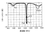
- FIG. 28 shows the antennas having the configurations shown in FIGS. 27A to 27D under the conditions in which the relative dielectric constant ⁇ of the dielectric is 4.9 and the dielectric loss tan ⁇ of the dielectric is 0.025. Shows the return loss as a result of simulation.
- the horizontal axis indicates the frequency
- the vertical axis indicates the return loss.
- line G1 shows the return loss of the line width W1 set to 20 mm.
- a broken line G2 indicates a return loss when the line width W1 is set to 0.2 mm.
- Fb03 is a resonance frequency of a harmonic that is three times the resonance mode B.
- the resonance frequency Fa0 of the resonance mode A and the resonance frequency Fb0 of the resonance mode B are separated, and furthermore, these Fa0 and Fb0 are in the relationship of the return loss improvement region satisfying the equations (69) and (72). You can see that Whether the resonance mode is A or B can be determined from the result of analyzing the current distribution by simulation.
- FIG. 28 shows that the return loss of the resonance frequency Fa0 in the resonance mode A can be improved to ⁇ 15 dB.
- the reason for this improvement is that the two resonance frequencies Fa0 and Fb03 are separated from each other and the resonance frequencies Fa0 and Fb03 are in the relationship of the improvement region of the return loss satisfying the equations (70) and (71).
- the line width W1 of a part (for example, the short side portions 29, 31) of the first element 23 is set to be, for example, 20 mm wider than the line width ⁇ i (for example, 0.2 mm) of the shape or the like.
- Fa0 and Fb03 satisfy the expressions (70) and (71).
- FIG. 29 and FIG. 30 show impedance charts and changes in return loss as a result of simulation for an antenna having a configuration in which the line width W1 is further increased and set to 29 mm, for example.
- the horizontal axis indicates the frequency
- the vertical axis indicates the return loss.
- a solid line G11 indicates a return loss when the line width W1 is set to 20 mm.
- a broken line G21 indicates a return loss when the line width W1 is set to 0.2 mm.
- a solid line G31 indicates a return loss when the line width W1 is set to 29 mm. From FIG. 30, it can be seen that if the line width W1 is increased from 0.2 mm to 20 mm, the return loss can be improved. However, if the line width W1 is excessively widened, for example, the return loss is deteriorated if the line width W1 is set to 29 mm.
- the line width W1 of at least a part of the line other than the inductance shape 34 of the first element 23 larger than the line width of the inductance shape 34, the return loss of the resonance frequency Fa0 can be improved, but the line width W1. It can also be seen that there is an optimum value (for example, 20 mm) for the width of the spread. If the line width W1 is further increased, for example, if it is larger than 29 mm, the line having the line width W1 (that is, the short side portions 29 and 31) and the semi-elliptical line having the inductance shape 34 are overlapped with each other. Stops functioning. Accordingly, the partial line width W1 of the first element 23 has an optimum value in terms of return loss performance improvement, and also has a physical upper limit value that overlaps with other lines.
- the configuration of the fifth embodiment other than that described above is the same as the configuration of the first embodiment. Accordingly, in the fifth embodiment, substantially the same operational effects as in the first embodiment can be obtained.
- FIG. 31A to FIG. 33D show a sixth embodiment of the present disclosure.
- symbol is attached
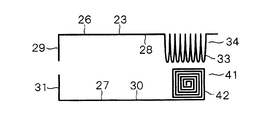
- an inductance shape having a rectangular spiral structure is used for a part of the line.
- the short circuit element 70 is not provided (that is, the first element 23 and the second element 24 are insulated from each other). The sixth embodiment will be specifically described below.
- the first element 23 includes a power supply side parallel portion 25 formed of a conductor pattern
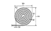
- the power supply side parallel portion 25 includes a first L-shaped portion 26 and a second L-shaped portion 27.
- the first L-shaped portion 26 includes a long side portion 28 and a short side portion 29.
- the second L-shaped portion 27 has the same configuration as the first L-shaped portion 26 and includes a long side portion 30 and a short side portion 31.
- the front ends of the short sides 29 and 31 are feeding points 32.
- first L-shaped portion 26 and the second L-shaped portion 27 are formed with inductance shapes 41 and 41 at the distal end portions of the long side portions 28 and 30 which are parts thereof.
- the inductance shape 41 protrudes in the inner direction surrounded by the first L-shaped portion 26 and the second L-shaped portion 27 in the plane of the substrate 22. As shown in FIG. 31 (d), the inductance shape 41 extends the linear conductor pattern of the long side portions 28 and 30 inward, and forms a rectangular spiral structure 42 at the extended portion.
- the line width ⁇ i of the conductor pattern of the rectangular spiral structure 42 is, for example, 0.2 mm
- the number of turns Nr of the rectangular spiral structure 42 is, for example, six times
- the gap Gr is 0.2 mm
- the width Wr of the rectangular spiral structure 42 is 4.9 mm
- the height Hr of the rectangular spiral structure 42 is 4.9 mm, for example.
- the longitudinal lengths (ie, element lengths) of the long side portions 28 and 30 of the first L-shaped portion 26 and the second L-shaped portion 27 are set to L (for example, 20 mm), and the long sides Of the lengths in the longitudinal direction of the portions 28 and 30, the length of the portion excluding the inductance shape 41 is Lm (for example, 15 mm), and the distance (element height) that the long side portions 28 and 30 are opposed to is H (for example, 12.4 mm). ).
- the line width of the long side portions 28 and 30 is the same as the line width of the inductance shape 41, and is ⁇ i (for example, 0.2 mm).
- the length of the short side portions 29 and 31 is S, and the line width of the short side portions 29 and 31 is the same as the line width of the inductance shape 41, and is ⁇ i (for example, 0.2 mm).
- the second element 24 includes a non-feeding side parallel portion 35 formed of a conductor pattern, and the non-feeding side parallel portion 35 includes a pair of opposing side portions 36 and 37.
- a connecting side 38 is provided.
- the opposing side portions 36 and 37 are parallel to each other, and have the same length and width.
- the opposing side portions 36 and 37 have the length L (that is, the element length) described above.
- the line widths of the opposing side portions 36 and 37 are W4 (for example, 5 mm), which is wider than the line width ⁇ i (for example, 0.2 mm) of the first L-shaped portion 26 and the second L-shaped portion 27.
- the connecting side portion 38 has a length (that is, an element height) of H, a line width of W2 (for example, 5 mm), and the lines of the first L-shaped portion 26 and the second L-shaped portion 27. It is wider than the width ⁇ i.
- Inductance shapes 43 and 43 are formed at the front ends of the opposing side portions 36 and 37.
- the inductance shape 43 protrudes in the inner direction surrounded by the opposing side portions 36 and 37 and the connecting side portion 38 in the plane of the substrate 22.
- the inductance shape 43 extends the conductor pattern having the line width ⁇ i from the center in the width direction of the opposing sides 36 and 37 in the direction along the opposing sides 36 and 37.
- a rectangular helical structure 42 is formed by the extended portion.
- the shape of the rectangular spiral structure 42 of the inductance shape 43 and the size of each part are the same as the shape of the rectangular spiral structure 42 of the inductance shape 41 and the size of each part.
- the element height H can be lowered by bending the lines of the first element 23 and the second element 24.
- the line width of the inductance formation 43 may be set to the minimum possible line width (that is, the lower limit value of the line width). Desirable in terms of miniaturization.
- the inductance shapes 41 and 43 have a rectangular spiral structure 42.
- the frequency ratio ⁇ fm at the boundary of the degradation range does not change so as to increase by one digit.
- the value of the equation (74) obtained by multiplying the value of the equation (73) by 10 is used as ⁇ fm.
- a solid line Y1 indicates that the relative dielectric constant ⁇ of the dielectric is set to 4.9, for example, and the dielectric loss tan ⁇ of the dielectric is set to 0.025, for example, and the conductivity of the conductor pattern (line) is copper (Cu).
- the return loss obtained is shown.
- the horizontal axis in FIG. 32 indicates the frequency, and the vertical axis indicates the return loss.
- the resonance frequency Fa0 of the resonance mode A and the resonance frequency Fb0 of the resonance mode B are separated, and furthermore, these Fa0 and Fb0 are in the relationship of the return loss improvement region satisfying the equations (69) and (72). You can see that Whether the resonance mode is A or B can be determined from the result of analyzing the current distribution by simulation.
- FIG. 32 shows that the return loss of the resonance frequency Fa0 in the resonance mode A can be improved from ⁇ 13 dB to ⁇ 17 dB by increasing the line widths W2 and W4 from 0.2 mm to 5 mm.
- the reason for this improvement is that the two resonance frequencies Fa0 and Fb0 are separated from each other, and the resonance frequencies Fa0 and Fb0 are in the relationship of the improvement region of the return loss that satisfies the equations (70) and (71).
- the line widths W2 and W4 of a part of the second element 24 are set to be 5 mm wider than the shape of the line width ⁇ i (for example, 0.2 mm). by.
- Fa0 and Fb0 satisfy the expressions (70) and (71).
- Faru 2106>
- Fb03 > 1368 ((1 + ⁇ fm) / (1 ⁇ fm)) Fa0 (71)
- the line width W2 of the connecting side portion 38 and the line width W4 of the opposite side portions 36 and 37 are optimal for the line width in terms of performance improvement of return loss.
- the configuration of the sixth embodiment other than that described above is the same as the configuration of the first embodiment. Therefore, in the sixth embodiment, substantially the same operational effects as in the first embodiment can be obtained.
- FIG. 33A to FIG. 34 illustrate a seventh embodiment of the present disclosure.
- symbol is attached
- a short-circuit element 70 for short-circuiting the first element 23 and the second element 24 is provided, and lines other than the inductance shapes 34 and 40 of the first element 23 and the second element 24 are provided. It was constituted so that there was no bent part in the part.
- the seventh embodiment will be specifically described below.
- the first element 23 includes a power supply side linear portion 45 formed by a conductor pattern, and the power supply side linear portions 45 are arranged so as to face each other. And a second linear portion 47.
- the front end portions of the first linear portion 46 and the second linear portion 47 that face each other serve as a feeding point 32.
- An inductance shape 34 is formed in the upper half portion in FIG. 33A which is a part of the first linear portion 46, and the lower portion in FIG. 33A which is a part of the second linear portion 47.
- An inductance shape 34 is formed in the half portion.
- the inductance shape 34 protrudes rightward in FIG. 33A in the plane of the substrate 22.
- the inductance shape 34 includes a conductor pattern having a line width ⁇ i from the center in the width direction of the first linear portion 46 and the second linear portion 47, and the first linear portion 46 and the second linear portion 46. It extends in the direction along the linear portion 47, and is formed by continuously forming Ni semi-elliptical inner protruding portions 33 at the extended portion.
- the width of the base of the inner protrusion 33 is Wi
- the height is Hi
- the line width is ⁇ i.
- the number of formed inner protrusions 33 for one inductance shape 34 is Ni.
- one semi-elliptical shape that is, the inner protrusion 33
- the inductance shape 34 since the number Ni of the semi-elliptical shape (that is, the inner protrusion 33) is, for example, 5, the inductance shape 34 has eleven bending structures.
- the length (element length) of the first linear portion 46 and the second linear portion 47 is set to L, and the length of the first linear portion 46 and the second linear portion 47 is set.
- the length of the portion excluding the inductance shape 34 is (Lm + S).
- the line width W1 of the first linear portion 46 and the second linear portion 47 excluding the inductance shape 34 is wider than the line width ⁇ i (for example, 0.2 mm) of the inductance shape 34.
- the element length L is, for example, 11.2 mm
- the length (Lm + S) to the inductance shape is, for example, 7.2 mm
- ⁇ i is, for example, 0.2 mm
- the line width W1 of the second linear portion 47 is 2 mm, for example, the semi-elliptical height Hi is 6 mm
- the semi-elliptical width Wi is 0.6 mm
- the thickness t of the dielectric (substrate 22) is 0.8 mm, for example. It is set to.
- the second element 24 includes a non-feeding side linear portion 48 formed by a conductor pattern.
- the line width of the non-feed-side linear portion 48 is the same as the line width ⁇ i (for example, 0.2 mm) of the conductor pattern of the portion where the inductance shape 34 of the first element 23 is formed.
- Inductance shapes 40 and 40 are formed at both ends of the non-feeding side linear portion 48. The inductance shape 40 protrudes leftward in FIG. 33C in the plane of the substrate 22. As shown in FIG.
- the inductance shape 40 extends the conductor pattern of the line width ⁇ i of the non-feed-side linear portion 48, and continuously extends the semi-elliptical inner protruding portion 33 to Ni at the extended portion. It is made up of individual pieces. Note that the shape of the inner protrusion 33 of the inductance shape 40 and the size of each part are the same as the shape of the inner protrusion 33 of the inductance shape 34 of the first element 23 and the size of each part.
- the first element 23 and the second element 24 are connected (short-circuited) by a short-circuit element 70.
- the short-circuit element 70 includes a through hole 71 that connects the upper end portion of the first linear portion 46 of the first element 23 and the upper end portion of the non-feeding side linear portion 48 of the second element 4,
- a through hole 71 is provided to connect the lower end portion of the second linear portion 47 of the element 23 and the lower end portion of the non-feeding side linear portion 48 of the second element 4.
- the short-circuit element 70 is provided, and the relationship between the two resonance frequencies Fa0 and Fb0 is within the return loss improvement region that satisfies the equations (69) and (72).
- the length (Lm + S) to the inductance shape is determined.
- the line width of the inductance formations 34 and 40 is set to the minimum possible line width (that is, the lower limit value of the line width). It is desirable from the viewpoint of miniaturization.
- the seventh embodiment there is no bending of the line portion other than the inductance shape, and the number of half ellipses Ni is 5.
- the frequency ratio ⁇ fm at the boundary of the deterioration range does not change so as to be an order of magnitude larger. Therefore, the value of the equation (74) obtained by multiplying the value of the equation (73) by 10 is used as ⁇ fm with a margin.
- a curve Z1 indicates that the relative dielectric constant ⁇ of the dielectric is set to 4.9, for example, and the dielectric loss tan ⁇ of the dielectric is set to 0.025, for example, and the conductivity of the conductor pattern (line) is copper (Cu).
- the return loss obtained is shown.
- the horizontal axis in FIG. 34 indicates the frequency, and the vertical axis indicates the return loss.
- a curve Z2 shown in FIG. 34 shows the return loss obtained as a result of simulating the configuration in which the line width W1 is set to 0.2 mm under the same conditions.
- the resonance frequency Fa0 of the resonance mode A and the resonance frequency Fb0 of the resonance mode B are separated, and furthermore, these Fa0 and Fb0 are in the relationship of the improvement region of the return loss satisfying the equations (69) and (72). You can see that Whether the resonance mode is A or B can be determined from the result of analyzing the current distribution by simulation.
- FIG. 34 shows that the return loss of the resonance frequency Fa0 of the resonance mode A can be improved from ⁇ 8 dB to ⁇ 13 dB by increasing the line width W1 from 0.2 mm to 2 mm.
- the reason for this improvement is that the two resonance frequencies Fa0 and Fb0 are separated from each other, and the resonance frequency Fa0 and Fb0 is in the relationship of the return loss improvement region satisfying the equations (69) and (72).
- the line width W1 of a part of the first element 23 (for example, the first linear portion 46 and the second linear portion 47) is set to 2 mm wider than the shape of the line width ⁇ i (for example, 0.2 mm). by.
- the line width W1 of a part of the first element 23 has an optimum value for the line width from the viewpoint of improving the performance of return loss.
- Fa0 and Fb0 satisfy the expressions (69) and (72).
- FIG. 35A to FIG. 35D illustrate the eighth embodiment of the present disclosure.
- symbol is attached
- the modified folded dipole antenna 21 of the fifth embodiment is provided on the printed wiring board 50 on which the high-frequency circuit 49 is mounted.
- the first element 23 of the first embodiment is formed on one surface of the printed wiring board 50, and as shown in FIG.
- the printed wiring board 50 is configured to have a dielectric function.
- connection lines 52 and 52 connecting the feeding point 32 and the input / output terminals 51a and 51b of the high-frequency circuit 49 are provided.
- the connection line 52 is formed of a conductor pattern (for example, a copper foil pattern), and its line width is, for example, ⁇ i.
- the configuration of the eighth embodiment other than that described above is the same as the configuration of the fifth embodiment. Therefore, in the eighth embodiment, substantially the same operational effects as in the fifth embodiment can be obtained.
- the modified folded dipole antenna 21 is provided on the printed wiring board 50 on which the high frequency circuit 49 is mounted, the number of parts can be reduced, and the input / output terminals of the high frequency circuit and the modified folded dipole antenna 21 can be reduced. Since the connection cable for connecting the cables can be made unnecessary, the manufacturing cost can be reduced.
- FIG. 36 shows a ninth embodiment of the present disclosure.
- symbol is attached
- the inner protruding portion 33 is formed to have an isosceles triangle shape.
- the shape of the inner protrusion 33 is different from that of the first embodiment, and the number, position, and size of the inner protrusion 33 are the same as those of the inner protrusion 33 of the first embodiment.
- the line width ⁇ i is the same as that of the inner protrusion 33 of the first embodiment.
- the inner protrusion 33 can be continuously formed even if the inner protrusion 33 has an isosceles triangle shape. Therefore, since many inner protrusions 33 can be formed in a narrow range, the antenna can be particularly miniaturized.
- FIG. 37 shows a tenth embodiment of the present disclosure.
- symbol is attached
- both end connection portions 54 that connect both ends of the inner protrusion 33 are further provided.
- the both ends connecting portion 54 connects one end and the other end of the semi-elliptical inner protruding portion 33.
- the both-end connecting portion 54 of the tenth embodiment has a semi-elliptical shape, and protrudes outward, unlike the inner protruding portion 33.
- the height of the both-end connecting portion 54 is L2 as shown in FIG.
- the inductance shapes 34 and 40 have a shape in which one or more elliptical shapes (inner protruding portions 33 + both end connecting portions 54) are arranged.
- the configuration of the tenth embodiment other than that described above is the same as the configuration of the first embodiment. Therefore, also in the tenth embodiment, substantially the same operational effects as in the first embodiment can be obtained.
- both end connection portions 54 that connect both ends of the inner protruding portion 33 are provided, it is possible to obtain an effect of preventing the return loss from fluttering.
- FIG. 38 shows an eleventh embodiment of the present disclosure.
- symbol is attached
- the inner protrusion 33 has a right-angled bent shape having two right-angled bending points.
- the height Hi and the line width ⁇ i of the inner protrusion 33 are the same as those of the inner protrusion 33 of the first embodiment thus far.
- the width of the repeating unit is the same as the width Wi of the inner protrusion 33 of the first embodiment.
- the number and position of the inner protrusions 33 are the same as in the first embodiment.
- the inductance shape is a shape in which one or more square shapes are arranged.
- FIG. 39 shows a twelfth embodiment of the present disclosure.
- symbol is attached
- the both-end connecting portion 55 connects one end and the other end of the inner protrusion 13 and has a semi-elliptical shape.
- both end connection portions 55 of the twelfth embodiment protrude inward as in the case of the inner protrusion 33.
- the protruding direction is different from the both-end connecting portion 54 of the fifth embodiment, but the height of the both-end connecting portion 55 is L2 as shown in FIG. 39, like the both-end connecting portion 54 of the tenth embodiment. .
- the configuration of the twelfth embodiment other than the above is the same as the configuration of the tenth embodiment. Therefore, in the twelfth embodiment, substantially the same operational effects as in the tenth embodiment can be obtained.
- FIG. 40 shows a thirteenth embodiment of the present disclosure.
- symbol is attached
- the inner protrusion 33 has a right triangle shape. Only the shape of the inner protrusion 33 is different from that of the first embodiment, and the number, position, and size of the inner protrusion 33 are the same as those of the first embodiment. Even when the inner protrusion 33 is a right triangle, since the tip is a point, the width of the tip is shorter than the length Wi of the base, and the width continuously decreases toward the tip. Therefore, even if the inner protrusion 33 is a right triangle, the inner protrusion 33 can be formed continuously. Therefore, since many inner protrusions 33 can be formed in a narrow range, the antenna can be particularly miniaturized.
- FIG. 41 shows a fourteenth embodiment of the present disclosure.
- symbol is attached
- the inner protrusion 33 has a step shape.
- the height Hi, the line width ⁇ i, and the repeat unit width Wi of the inner protrusion 33 are the same as those of the inner protrusion 3 of the first embodiment.
- the number and position of the inner protrusions 33 are the same as those in the first embodiment.
- the shape of one inner projecting portion 33 is the first long perpendicular portion 33a, the tip line portion 33b, the first short perpendicular portion 33c, the intermediate line portion 33d, and the second short perpendicular portion 33e.
- the first long perpendicular portion 33a extends from the one end point e of the inner protruding portion 33 to the tip of the inner protruding portion 33 toward the center plane C in the antenna width direction.
- the tip line portion 33b has one end connected to the tip end side end of the first long perpendicular portion 33a and is parallel to the center plane C in the antenna width direction.
- the first short perpendicular portion 33c is connected at one end to the distal end line portion 33b, and extends from the distal end line portion 33b in a direction perpendicular to the antenna width direction center plane C and away from the antenna width direction center plane C. . Moreover, the 1st short perpendicular part 33c is shorter than the 1st long perpendicular part 33a.
- the intermediate line portion 33d has one end connected to the first short perpendicular portion 33c, and extends from the first short perpendicular portion 33c in parallel to the center plane C in the antenna width direction and opposite to the first long perpendicular portion 33a. .
- the second short perpendicular part 33e has one end connected to the intermediate line part 33d and the other end becomes an end point e of the inner projecting part 33 opposite to the side to which the first long perpendicular part 33a is connected. It is perpendicular to the center plane C in the antenna width direction.
- the second short perpendicular portion 33e is shorter than the first long perpendicular portion 33a.
- the inner protruding portion 33 having the above-described configuration is connected to the adjacent inner protruding portion 33 through the short connection line 33f. Even when the inner projecting portion 33 has a step shape, the length of the inner projecting portion 33 is longer than the case where there is no inner projecting portion 33, so that the antenna can be downsized.
- FIG. 42 shows a fifteenth embodiment of the present disclosure.
- symbol is attached
- an elliptical helical structure 60 is formed by a conductor pattern having a line width ⁇ i, and an inductance shape 41 is configured by the formed elliptical helical structure 60.
- the line width of the conductor pattern of the elliptical helical structure 60 is ⁇ i
- the number of turns of the elliptical helical structure 60 is Nr
- the gap of the elliptical helical structure 60 is Gr
- the width of the elliptical helical structure 60 is Is Wr
- the height of the elliptical helical structure 60 is Hr.
- the configuration of the fifteenth embodiment other than that described above is the same as the configuration of the sixth embodiment. Therefore, in the fifteenth embodiment, substantially the same operational effects as in the sixth embodiment can be obtained.
- FIG. 43 shows a sixteenth embodiment of the present disclosure.
- a circular spiral structure 61 is formed by a conductor pattern having a line width ⁇ i, and an inductance shape 41 is configured by the circular spiral structure 61 thus formed.
- the line width of the conductor pattern of the circular helical structure 61 is ⁇ i
- the number of turns of the circular helical structure 61 is Nr
- the gap of the circular helical structure 61 is Gr
- the width of the circular helical structure 61 is Wr
- circular The height of the helical structure 61 is Hr.
- the configuration of the sixteenth embodiment other than that described above is the same as the configuration of the fifteenth embodiment. Therefore, in the sixteenth embodiment, substantially the same operational effects as in the fifteenth embodiment can be obtained.
- FIG. 44 shows a seventeenth embodiment of the present disclosure.
- symbol is attached
- the long-side portions 28 and 30 of the first L-shaped portion 26 and the second L-shaped portion 27 of the first element 23 are provided with the inductance shapes 34 and 34 having the same shape.
- a different inductance shape may be provided.
- an inductance shape 34 including an inward protruding portion 33 is provided on the long side portion 28 of the first L-shaped portion 26 of the first element 23.
- An inductance shape 41 composed of a rectangular spiral structure 42 is provided on the long side portion 30 of the second L-shaped portion 27.
- an inductance shape 34 including an inward protruding portion 33 is provided on the opposite side portion 36 corresponding to the first L-shaped portion 26.
- An inductance shape 41 composed of a rectangular spiral structure 42 is provided on the opposite side portion 37 corresponding to the 2L-shaped portion 27.
- the configuration of the seventeenth embodiment other than that described above is the same as the configuration of the first embodiment or the sixth embodiment. Accordingly, in the seventeenth embodiment, substantially the same operational effects as those of the first or sixth embodiment can be obtained.
- an inductance shape 34 composed of the inner protruding portions 33 having different shapes is provided. It may be configured to be combined, may be configured to combine inductance shapes composed of spiral structures 42, 60, 61 of different shapes, or one of a plurality of types of inner protrusions and a plurality of types of spirals You may comprise so that one of the structures may be combined suitably.
- FIG. 45 shows an eighteenth embodiment of the present disclosure.
- symbol is attached
- the first L-shaped portion 26 of the first element 23 and the long side portions 28 and 30 of the second L-shaped portion 27 are provided with inductance shapes 34 and 34 having the same shape and the same number of inward protruding portions 33.
- the present invention is not limited to this, and an inductance shape in which the number of the inner protrusions 33 is different may be provided.
- the eighteenth embodiment as shown in FIG.
- each inner protrusion 33 is formed on the long side portion 28 of the first L-shaped portion 26 of the first element 23, and for example, six inner protrusions 33 are formed on the long side portion 30 of the second L-shaped portion 27.
- eight inward protruding portions 33 are formed on the opposing side portion 36 corresponding to the first L-shaped portion 26,
- six inward protruding portions 33 are formed on the opposite side portion 37 corresponding to the 2L-shaped portion 27.
- the configuration of the eighteenth embodiment other than that described above is the same as the configuration of the first embodiment. Accordingly, in the eighteenth embodiment, substantially the same operational effects as in the first embodiment can be obtained.
- the number of semi-elliptical inner protrusions 33 formed is different.
- the present invention is not limited to this, and the number of other inner protrusions 33 formed is different. You may comprise.
- the modified folded dipole antenna 21 of each embodiment described above can be used as a small antenna for an in-vehicle wireless device or a mobile terminal (smartphone, mobile phone, etc.).
- wireless communication systems for in-vehicle wireless devices and portable terminals include cellular phones (700 MHz band, 800 MHz band, 900 MHz band, 1.5 GHz band, 1.7 GHz band, 2 GHz band), wireless LAN (2.4 GHz band, 5 GHz band), GPS (1.5 GHz band), inter-vehicle communication (700 MHz band), road-to-vehicle communication (5.8 GHz band), and the like.
- the return loss can be improved. Also, the return loss is improved both when the lines other than the inductance shape of the first element and the second element are bent (first to sixth embodiments) or when the lines are not bent (seventh embodiment). be able to.
- (Nineteenth embodiment) 46 to 49 show a nineteenth embodiment of the present disclosure.
- symbol is attached
- the calculation device 81 for antenna design includes an input unit 82, an antenna characteristic constant storage unit 83, a calculation unit 84, and an output unit 85.
- the input unit 82 includes a keyboard, a mouse, and the like, and inputs data such as resonance frequencies Fa0 and Fb0 and calculation conditions (for example, Fk, Fo, and Fs).
- the antenna characteristic constant storage unit 83 includes a storage unit such as a memory or a hard disk, and various antenna characteristic constants (for example, Kau, Kad, Far, Fard, Ra, Kbu, Kbd, Fbru, Fbrd, Rb) and the like are stored.
- the calculation unit 84 is preferably configured to transmit the calculation result to the antenna characteristic constant storage unit 83 and store it.
- the output unit 85 includes a display device, a printer, a communication device that transmits to an external device, and the like.
- the calculation result received from the calculation unit 84 is displayed on the display device, printed by the printer, or transmitted to the external device. Or send.
- step S10 of FIG. 47 the calculation unit 84 inputs the resonance frequencies Fa0 and Fb0 input by the input unit 82 and frequency calculation conditions (for example, Fk, Fo, Fs).
- Fk is a calculation start frequency
- Fo is a calculation end frequency
- Fs is a calculation step frequency (that is, an interval between frequencies to be calculated)
- a frequency range to be calculated is determined by these calculation conditions. .
- step S20 the calculation unit 84 calculates the antenna characteristic constants stored in the antenna characteristic constant storage unit 83 (for example, Kau, Kad, Far, Fard, Ra, Kbu, Kbd, Fbru, Fbrd, Rb). Read and input.
- Kau and Kad are proportional constants above and below the resonance mode A (that is, Equation (31) or (33), Equation (30) or (32)).
- Faru and Fard are a high antiresonance frequency (ie, equation (7b)) and a low antiresonance frequency (ie, equation (7a)) of the resonance mode A.
- Ra is the resonance resistance of the resonance mode A (see FIG. 13 or FIG. 15).
- Kbu and Kbd are proportional constants above and below resonance mode B (that is, equation (36) or (38), equation (35) or (37)).
- Fbru and Fbrd are the high antiresonance frequency (that is, the equation (8b) or (9b)) and the low antiresonance frequency (that is, the equation (8a) or (9a)) of the resonance mode B.
- Rb is the resonance resistance of resonance mode B (see FIG. 14 or FIG. 15).
- step S30 the frequency F to be calculated is set as the calculation start frequency Fk. Thereafter, the process proceeds to step S40, and it is determined whether F is Fa0 or less. Here, if F is equal to or less than Fa0, the process proceeds to step S50, and the reactance Xa of the resonance mode A is calculated by the equation (11). In step S40, when F is larger than Fa0, the process proceeds to step S60, and reactance Xa of the resonance mode A is calculated by the equation (14).
- step S70 it is determined whether F is equal to or less than Fb0.
- Fb0 the process proceeds to step S80, and the reactance Xb of the resonance mode B is calculated by the equation (18).
- step S70 when F is larger than Fb0, the process proceeds to step S90, and the reactance Xb of the resonance mode B is calculated by the equation (21).
- step S100 the impedances Za and Zb of the resonance modes A and B are calculated by the equations (10) and (17).
- step S110 the admittances Ya and Yb of the resonance modes A and B are calculated by the equations (24) and (25).
- step S120 the combined admittance Yab, reflection coefficient ⁇ ab, and return loss RLab of resonance modes A and B are calculated using equations (26), (27), and (28).
- step S130 the calculation unit 84 outputs the calculation results (F, Yab, Zab, ⁇ ab, RLab) to the output unit 85.
- the calculation unit 84 may be configured to transmit the calculation result to the antenna characteristic constant storage unit 83 and store it.
- step S140 it is determined whether or not the frequency F is equal to or higher than the end frequency Fo. If the frequency F is less than the end frequency Fo, the process proceeds to step S150, the calculation step frequency Fs is added to the frequency F, the process returns to step S40, and the above-described processing is repeated. In step S140, when the frequency F is equal to or higher than the end frequency Fo, the process proceeds to “YES” to end the calculation control.
- FIG. 48 An example of the calculation result of the return loss RLab is shown in FIG.
- the horizontal axis represents frequency
- the vertical axis represents return loss.
- Fa0 900 MHz
- Fb0 1000 MHz
- Fk 700 MHz
- Fo 1200 MHz
- Fs 1 MHz.
- the antenna characteristic constants for example, Kau, Kad, Faru, Fard, Ra, Kbu, Kbd, Fbru, Fbrd, Rb
- FIG. 48 and 49 show examples of output by the output unit 85.
- (20th embodiment) 50 to 53 show a twentieth embodiment of the present disclosure.
- the same components as those in the nineteenth embodiment are given the same reference numerals.
- one resonance frequency F1 of the resonance frequencies Fa0 and Fb0 of the resonance modes A and B is input, and another resonance frequency F2a and F2b and the inductance shape when the antenna shape is changed.
- (Lm + S) a and (Lm + S) b are calculated.
- the number Ni of the inner protrusions 33 of the inductance shape 34 is changed.
- the input unit 82 inputs data of one resonance frequency F1 among the resonance frequencies Fa0 and Fb0 of the resonance modes A and B.
- an antenna shape constant storage unit 86 is provided in place of the antenna characteristic constant storage unit 83.
- the antenna shape constant storage unit 86 as the antenna shape constant, 2 at the time of resonance when the number Ni of the inner protrusions 33 is changed is provided.
- Proportional constants Ca1 (Ni) for two wavelengths ⁇ a and ⁇ b see equation (3)
- Cb1 (Ni) see equation (4)
- constants Ca0 (Ni) for two wavelengths ⁇ a and ⁇ b (equation (3) Reference) and Cb0 (Ni) (see equation (4)).
- the calculation unit 84 receives one resonance frequency F1 input from the input unit 82, and receives antenna shape constants (Ca1 (Ni), Cb1 (Ni), Ca0 (Ni), Cb0 (Ni)) from the antenna shape constant storage unit 86. ), The other resonance frequencies F2a and F2b and the lengths (Lm + S) a and (Lm + S) b to the inductance shape are calculated, and the calculation results are transmitted to the output unit 85.
- the calculation unit 84 is preferably configured to transmit the calculation result to the antenna shape constant storage unit 86 for storage.
- the output unit 85 displays the calculation result received from the calculation unit 84 on a display device, prints it with a printer, or transmits it to an external device.
- the flowchart of FIG. 51 shows the control contents of the calculation program of the calculation unit 84.
- this calculation process while changing the number Ni of the inner protrusions 33 from 1 to the maximum number (Nmax), another resonance frequency F2a, F2b and the length to the inductance shape (Lm + S) a, (Lm + S) b is calculated.
- step S ⁇ b> 210 of FIG. 51 the calculation unit 84 inputs one resonance frequency F ⁇ b> 1 input by the input unit 82 and reads and inputs the antenna shape constant stored in the antenna shape constant storage unit 86. . Then, it progresses to step S220 and sets 1 to the number Ni.
- step S230 the resonance frequencies F2a and F2b and the lengths (Lm + S) a and (Lm + S) b are calculated based on the equations (3), (4), (5), and (6). .
- step S240 the process proceeds to step S240, and the calculation unit 84 transmits Ni, (Lm + S) a, F2a, (Lm + S) b, and F2b to the output unit 85.
- step S250 it is determined whether Ni is Nmax or more.
- Ni is smaller than Nmax
- step S260 the process proceeds to step S260, and Ni is counted up (ie, +1). And it progresses to step S230 and performs the process mentioned above repeatedly.
- Step S250 when Ni is greater than or equal to Nmax, the process proceeds to “YES” and the calculation process is terminated.
- the solid line FN1 indicates the resonance frequency F2a
- the solid line FN2 indicates the resonance frequency F2b
- the solid line FN3 indicates the resonance frequency F1.
- a solid line LN1 indicates a length (Lm + S) a
- a solid line LN2 indicates a length (Lm + S) b.
- 16 is a through hole
- 21 is a modified folded dipole antenna
- 22 is a substrate
- 23 is a first element
- 24 is a second element
- 26 is a first L-shaped part
- 27 is a second L-shaped part
- 28 is long.
- 72 1 element, 73 is a wide conductor, 74 is an input terminal, 75 is a second element, 76 is an L-shaped part, 77 is an input terminal, 78 is a high-frequency circuit, 81 is a computing device, 82 is an input unit, and 83 is an antenna A characteristic constant storage unit, 84 is a calculation unit, 85 is an output unit, and 86 is an antenna shape constant storage unit.
- each section is expressed as S10, for example.
- each section can be divided into a plurality of subsections, while a plurality of sections can be combined into one section.
- each section configured in this manner can be referred to as a device, module, or means.
Landscapes
- Details Of Aerials (AREA)
Abstract
小型アンテナは、給電点(32)を有する一対の導体からなる第1素子(23)と、誘電体を挟んで配置され、導体である第2素子(24)とを備える。前記第1および第二素子(23、24)の一部が、インダクタンス形状(34、40、41)になっている。前記第1および第二素子(23、24)が同一電流方向の第一共振モード(A)は、第一共振周波数(Fa0)を有する。前記第1および第二素子(23、24)が逆電流方向の第二共振モード(B)は、第二共振周波数(Fb0)を有する。第一共振周波数(Fa0)が、第二共振周波数(Fb0)のわずかに上から第二共振モード(B)の高い反共振周波数(Fbru)までの範囲か、第二共振周波数(Fb0)のわずかに下から共振モード(B)の低い反共振周波数(Fbrd)までの範囲に入るように、給電点からインダクタンス形状までの長さ(Lm+S)が設定されている。
Description
本出願は、2015年7月31日に出願された日本特許出願番号2015-152027号および2015年12月14日に出願された日本特許出願番号2015―243143号に基づくもので、ここにその記載内容を援用する。
本開示は、変形折り返しダイポールアンテナを小型化することができる小型アンテナ及び計算装置に関するものである。
特許文献1には、線路からなる導体でダイポールアンテナを構成する第1の素子と、絶縁体を挟んで第1の素子に対向して配置され、線路からなる導体である第2の素子とを備えた変形折り返しダイポールアンテナが記載されている。この変形折り返しダイポールアンテナでは、第1の素子の先端と第2の素子の先端を接続し、更に、第1の素子と第2の素子を折り曲げている。この変形折り返しダイポールアンテナをさらに小型化した小型アンテナとして、特許文献2に記載された小型アンテナが知られている。この小型アンテナでは、変形折り返しダイポールアンテナのエレメントの直線部分の一部を、インダクタンス形状(クランク形状や先端にいくほど形状幅が小さくなる形状、例えば、三角形や半楕円の形状)となるように構成した。
一方、変形折り返しダイポールアンテナのリターンロスを改善したアンテナとして、特許文献3に記載された構成が知られている。この構成では、変形折り返しダイポールアンテナの素子の線幅を調整することにより、インピーダンスを調整して、リターンロスを改善している。
リターンロスを改善した変形折り返しダイポールアンテナ(特許文献3参照)は、小型化が困難であるという問題がある。一方、直線部分の一部をインダクタンス形状にして、小型化したダイポールアンテナ(特許文献2参照)は、特許文献3の構成を適用しても、リターンロスを良好に改善することが困難であるという問題がある。
本開示は、小型化を図ることができると共に、リターンロスを向上させることができる小型アンテナ及び計算装置を提供することを目的とする。
本開示の第一の態様において、小型アンテナは、線路からなる一対の導体からなり、当該一対の導体の各々における片方の端部が給電点である第1の素子と、誘電体を挟んで前記第1の素子に対向して配置され、線路からなる導体である第2の素子とを備える。前記第1の素子と前記第2の素子の線路の一部が、三箇所以上の曲げ構造のインダクタンス形状、または、らせん構造のインダクタンス形状になっている。前記第1の素子に流れる電流方向と前記第2の素子に流れる電流方向が同一方向の第一共振モードは、第一共振周波数を有する。前記第1の素子に流れる電流方向と前記第2の素子に流れる電流方向が逆方向の第二共振モードは、第二共振周波数を有する。第一共振モードの第一共振周波数が、第二共振モードの第二共振周波数のわずかに上から第二共振モードの高い反共振周波数までの範囲か、第二共振モードの第二共振周波数のわずかに下から共振モードの低い反共振周波数までの範囲に入るように、給電点からインダクタンス形状までの長さが設定されている。
本開示の第二の態様において、小型アンテナは、線路と広い導体からなる第1の素子と、誘電体を挟んで前記第1の素子の線路部に対向して配置され、線路からなる導体である第2の素子とを備える。前記第1の素子の線路と広い導体の接続部と第2の素子の端部に、給電点がある。前記第1の素子と前記第2の素子の線路の一部が、三箇所以上の曲げ構造のインダクタンス形状、または、らせん構造のインダクタンス形状になっている。前記第1の素子に流れる電流方向と前記第2の素子に流れる電流方向が同一方向の第一共振モードは、第一共振周波数を有する。前記第1の素子に流れる電流方向と前記第2の素子に流れる電流方向が逆方向の第二共振モードは、第二共振周波数を有する。第一共振モードの第一共振周波数が、第二共振モードの第二共振周波数のわずかに上から第二共振モードの高い反共振周波数までの範囲か、第二共振モードの第二共振周波数のわずかに下から第二共振モードの低い反共振周波数までの範囲に入るように、給電点からインダクタンス形状までの長さが設定されている。
本開示の第三の態様において、アンテナ設計用の計算装置は、線路からなる一対の導体からなり、当該一対の導体の各々における片方の端部が給電点である第1の素子と、誘電体を挟んで前記第1の素子に対向して配置され、線路からなる導体である第2の素子とを備えた小型アンテナであって、前記第1の素子と前記第2の素子の線路の一部が、三箇所以上の曲げ構造のインダクタンス形状、または、らせん構造のインダクタンス形状になっている小型アンテナについて、第一共振周波数と第二共振周波数とを入力して、前記小型アンテナのアドミッタンス、インピーダンス、反射係数、または、リターンロスを計算する。前記第1の素子に流れる電流方向と前記第2の素子に流れる電流方向が同一方向の第一共振モードは、第一共振周波数を有する。前記第1の素子に流れる電流方向と前記第2の素子に流れる電流方向が逆方向の第二共振モードは、第二共振周波数を有する。
本開示の第四の態様において、アンテナ設計用の計算装置は、線路と広い導体からなる第1の素子と、誘電体を挟んで前記第1の素子の線路部に対向して配置され、線路からなる導体である第2の素子とを備え、前記第1の素子の線路と広い導体の接続部と第2の素子の端部に、給電点がある小型アンテナであって、前記第1の素子と前記第2の素子の線路の一部が、三箇所以上の曲げ構造のインダクタンス形状、または、らせん構造のインダクタンス形状になっている小型アンテナについて、第一共振周波数と第二共振周波数とを入力して、前記小型アンテナのアドミッタンス、インピーダンス、反射係数、または、リターンロスを計算する。前記第1の素子に流れる電流方向と前記第2の素子に流れる電流方向が同一方向の第一共振モードは、第一共振周波数を有する。前記第1の素子に流れる電流方向と前記第2の素子に流れる電流方向が逆方向の第二共振モードは、第二共振周波数を有する。
本開示の第五の態様において、アンテナ設計用の計算装置は、線路からなる一対の導体からなり、当該一対の導体の各々における片方の端部が給電点である第1の素子と、誘電体を挟んで前記第1の素子に対向して配置され、線路からなる導体である第2の素子とを備えた小型アンテナであって、前記第1の素子と前記第2の素子の線路の一部が、三箇所以上の曲げ構造のインダクタンス形状、または、らせん構造のインダクタンス形状になっている小型アンテナについて、前記第1の素子と前記第2の素子の一つの共振周波数を入力して、前記第1の素子と前記第2の素子の他の一つの共振周波数、または、アンテナ形状を計算する。
本開示の第六の態様において、アンテナ設計用の計算装置は、線路と広い導体からなる第1の素子と、誘電体を挟んで前記第1の素子の線路部に対向して配置され、線路からなる導体である第2の素子とを備え、前記第1の素子の線路と広い導体の接続部と第2の素子の端部に、給電点がある小型アンテナであって、前記第1の素子と前記第2の素子の線路の一部が、三箇所以上の曲げ構造のインダクタンス形状、または、らせん構造のインダクタンス形状になっている小型アンテナについて、前記第1の素子と前記第2の素子の一つの共振周波数を入力して、前記第1の素子と前記第2の素子の他の一つの共振周波数、または、アンテナ形状を計算する。
本開示の第七の態様において、小型アンテナは、線路からなる一対の導体からなり、当該一対の導体の片方の端部が給電点である第1の素子と、誘電体を挟んで前記第1の素子に対向して配置され、線路からなる導体である第2の素子とを備える。前記第1の素子と前記第2の素子の線路の一部が、三箇所以上の曲げ構造を有するインダクタンス形状、または、らせん構造を有するインダクタンス形状になっている。前記第1の素子に流れる電流方向と前記第2の素子に流れる電流方向が同一方向の第一共振モードの第一共振周波数と、前記第1の素子に流れる電流方向と前記第2の素子に流れる電流方向が逆方向の第二共振モードの第二共振周波数が離れるように、前記第1の素子及び前記第2の素子の中心からインダクタンス形状までの長さを設定する。前記第1の素子または前記第2の素子の線路のうちの前記インダクタンス形状以外の線路の少なくとも一部の線路幅が、前記インダクタンス形状の線路の線路幅よりも広くなるように構成されている。
上記の各態様において、小型化を図ることができると共に、リターンロスを向上させることができる。
本開示についての上記目的およびその他の目的、特徴や利点は、添付の図面を参照しながら下記の詳細な記述により、より明確になる。その図面は、
図1(a)から図1(d)は、本開示の第1実施形態を示すもので、図1(a)は変形折り返しダイポールアンテナの第1の素子側の構成を示す図、図1(b)は変形折り返しダイポールアンテナの縦断側面図、図1(c)は変形折り返しダイポールアンテナの第2の素子側の構成を示す図、図1(d)はインダクタンス形状の拡大図であり、
図2は、周波数と長さ(Lm+S)との関係を示す特性図であり、
図3(a)から図3(c)は、従来構成(その1)を示すもので、図3(a)は変形折り返しダイポールアンテナの第1の素子側の構成を示す図、図3(b)は変形折り返しダイポールアンテナの縦断側面図、図3(c)は変形折り返しダイポールアンテナの第2の素子側の構成を示す図であり、
図4(a)から図4(c)は、従来構成(その2)を示すもので、図4(a)は変形折り返しダイポールアンテナの第1の素子側の構成を示す図、図4(b)は変形折り返しダイポールアンテナの縦断側面図、図4(c)は変形折り返しダイポールアンテナの第2の素子側の構成を示す図であり、
図5は、共振周波数とエレメント長との関係を示す特性図であり、
図6は、リターンロスと周波数との関係を示す特性図であり、
図7は、共振波長と長さ(Lm+S)との関係を示す特性図であり、
図8は、リターンロスと周波数との関係を示す特性図であり、
図9は、インピーダンスチャートを示す図であり、
図10(a)から図10(c)は、本開示を説明する構成(その1)を示すもので、図10(a)は変形折り返しダイポールアンテナの第1の素子側の構成を示す図、図10(b)は変形折り返しダイポールアンテナの縦断側面図、図10(c)は変形折り返しダイポールアンテナの第2の素子側の構成を示す図であり、
図11は、リターンロスと周波数との関係を示す特性図であり、
図12は、規格化周波数とFa0/Fb0との関係を示す特性図であり、
図13は、インピーダンスZaのスミスチャートであり、
図14は、インピーダンスZbのスミスチャートであり、
図15は、インピーダンスのシミュレーション結果を示すスミスチャートであり、
図16は、各周波数及び各定数を表にして示す図であり、
図17は、シミュレーション結果と計算結果を比較するスミスチャートであり、
図18は、シミュレーション結果と計算結果を比較するものであって、リターンロスと周波数との関係を示す特性図であり、
図19は、シミュレーション結果と計算結果を比較するスミスチャートであり、
図20は、シミュレーション結果と計算結果を比較するものであって、リターンロスと周波数との関係を示す特性図であり、
図21は、本開示の第2実施形態を示すもので、周波数と長さ(Lm+S)との関係を示す特性図であり、
図22(a)から図22(c)は、本開示の第3実施形態を示すもので、図22(a)は変形折り返しモノポールアンテナの第1の素子側の構成を示す図、図22(b)は変形折り返しモノポールアンテナの縦断側面図、図22(c)は変形折り返しモノポールアンテナの第2の素子側の構成を示す図であり、
図23は、周波数と長さ(Lm+S)との関係を示す特性図であり、
図24は、リターンロスと周波数との関係を示す特性図であり、
図25は、共振波長と長さ(Lm+S)との関係を示す特性図であり、
図26は、本開示の第4実施形態を示すもので、周波数と長さ(Lm+S)との関係を示す特性図であり、
図27(a)から図27(d)は、本開示の第5実施形態を示すもので、図27(a)は変形折り返しダイポールアンテナの第1の素子側の構成を示す図、図27(b)は変形折り返しダイポールアンテナの縦断側面図、図27(c)は変形折り返しダイポールアンテナの第2の素子側の構成を示す図、図27(d)はインダクタンス形状の拡大図であり、
図28は、リターンロスと周波数との関係を示す特性図であり、
図29は、インピーダンスチャートを示す図であり、
図30は、リターンロスと周波数との関係を示す特性図であり、
図31(a)から図31(d)は、本開示の第6実施形態を示すもので、図31(a)は変形折り返しダイポールアンテナの第1の素子側の構成を示す図、図31(b)は変形折り返しダイポールアンテナの縦断側面図、図31(c)は変形折り返しダイポールアンテナの第2の素子側の構成を示す図、図31(d)はインダクタンス形状の拡大図であり、
図32は、リターンロスと周波数との関係を示す特性図であり、
図33(a)から図33(d)は、本開示の第7実施形態を示すもので、図33(a)は変形折り返しダイポールアンテナの第1の素子側の構成を示す図、図33(b)は変形折り返しダイポールアンテナの縦断側面図、図33(c)は変形折り返しダイポールアンテナの第2の素子側の構成を示す図、図33(d)はインダクタンス形状の拡大図であり、
図34は、リターンロスと周波数との関係を示す特性図であり、
図35(a)から図35(b)は、本開示の第8実施形態を示すもので、図35(a)は変形折り返しダイポールアンテナの第1の素子側の構成を示す図、図35(b)は変形折り返しダイポールアンテナの第2の素子側の構成を示す図であり、
図36は、本開示の第9実施形態を示すインダクタンス形状の拡大図であり、
図37は、本開示の第10実施形態を示すインダクタンス形状の拡大図であり、
図38は、本開示の第11実施形態を示すインダクタンス形状の拡大図であり、
図39は、本開示の第12実施形態を示すインダクタンス形状の拡大図であり、
図40は、本開示の第13実施形態を示すインダクタンス形状の拡大図であり、
図41は、本開示の第14実施形態を示すインダクタンス形状の拡大図であり、
図42は、本開示の第15実施形態を示すインダクタンス形状の拡大図であり、
図43は、本開示の第16実施形態を示すインダクタンス形状の拡大図であり、
図44は、本開示の第17実施形態を示すもので、変形折り返しダイポールアンテナの第1の素子側の構成を示す図であり、
図45は、本開示の第18実施形態を示すもので、変形折り返しダイポールアンテナの第1の素子側の構成を示す図であり、
図46は、本開示の第19実施形態を示す計算装置のブロック図であり、
図47は、計算制御のフローチャートであり、
図48は、リターンロスと周波数との関係を示す特性図であり、
図49は、スミスチャートであり、
図50は、本開示の第20実施形態を示す計算装置のブロック図であり、
図51は、計算制御のフローチャートであり、
図52は、共振周波数と半楕円形状の個数との関係を示す特性図であり、
図53は、長さ(Lm+S)と半楕円形状の個数との関係を示す特性図である。
以下、本開示の第1実施形態について、図1(a)ないし図20を参照して説明する。本開示は、特許文献2に記載された変形折り返しダイポールアンテナを改良することにより、リターンロスを改善したものである。まず、本発明者による開示の過程について説明する。
図4(a)から図4(c)に、特許文献2の変形折り返しダイポールアンテナ1を示す。この変形折り返しダイポールアンテナ1は、誘電体の基板2(図4(b)参照)の一方の面に導体パターン(線路からなる導体)で形成された第1の素子3と、誘電体の基板2の他方の面に導体パターンで形成された第2の素子4と、第1の素子3と第2の素子4を短絡する短絡素子5とを備える。
第1の素子3は、図4(a)に示すように、アンテナ幅方向中心面Cに対して対称となっている第1L字部6及び第2L字部7を有し、これらL字部6、7の各長辺部の先端部にはインダクタンス形状8、9が設けられている。L字部6、7の各短辺部の先端部の対向する部位に、給電点10が設けられている。第2の素子4は、図4(c)に示すように、第1の素子3とほぼ同形状に形成されており、一対の対向辺部11、12と、これら対向辺部11、12の一端を連結する連結辺部13とを有している、対向辺部11、12の各他端部にはインダクタンス形状14、15が設けられている。短絡素子5は、第1の素子3のL字部6、7の各先端部と、第2の素子4の対向辺部11、12の各他端部の先端とを接続するスルーホール16(図4(b)参照)を備えている。
また、図3(a)から図3(c)には、第1の素子3のL字部6、7と、第2の素子4の対向辺部11、12とに、インダクタンス形状8、9、14、15を設けないように構成した変形折り返しダイポールアンテナ17を示す。
このような構成の変形折り返しダイポールアンテナ1、17においては、第1の素子3と第2の素子4とに流れる電流の方向が同一方向である共振モード(共振モードAと称する)と、第1の素子3と第2の素子4とに流れる電流の方向が逆方向である共振モード(共振モードBと称する)とがある。ここで、第1の素子3及び第2の素子4の長辺部(即ち、L字部6、7の長辺部、対向辺部11、12の長辺部)の長さをLとし、Lを変化させたときの共振モードA、Bの共振周波数Fa0、Fb0の変化をシミュレーションした結果を、図5に示す。図5においては、横軸をL(エレメント長)とし、縦軸を共振周波数としている。
図5において、曲線P1は、変形折り返しダイポールアンテナ17(図3(a)から図3(c)参照)の共振モードAの共振周波数Fa0の変化を示し、曲線P2は、変形折り返しダイポールアンテナ12の共振モードBの共振周波数Fb0の変化を示す。そして、曲線P3は、変形折り返しダイポールアンテナ1(図4(a)から図4(c)参照)の共振モードAの共振周波数Fa0の変化を示し、曲線P4は、変形折り返しダイポールアンテナ1の共振モードBの共振周波数Fb0の変化を示す。
上記図5のグラフから、第1の素子3及び第2の素子4の線路の一部をインダクタンス形状8、9、14、15に変更することにより、次の2つの変化が発生することがわかる。第1の変化は、2つの共振モードA、Bの共振周波数Fa0、Fb0が低くなることである。第2の変化は、2つの共振モードA、Bの共振周波数Fa0、Fb0が接近し、一致する場合も発生することである。
特許文献2に記載された変形折り返しダイポールアンテナ1は、第1の変化の作用効果に着目してなされたものである。これに対して、第2の変化が起こると、2つの共振周波数Fa0、Fb0がほぼ一致してしまい、2つの共振モードが影響し合うようになり、リターンロスが大きくなることがわかった。そこで、本発明者は、第1の素子3及び第2の素子4の線路の一部をインダクタンス形状8、9、14、15に変更した構成としながら、2つの共振周波数Fa0、Fb0を離間させる構成を開示することにより、リターンロスの改善を試みた。
具体的には、まず、図4(a)に示すように、第1の素子3(及び第2の素子4)のL字部6の短辺部の長さをSとし、L字部6の長辺部のうちのインダクタンス8を除く部分の長さをLmとし、長さ(Lm+S)を変化させることにより、2つの共振モードA、Bの2つの波長λa、λbを離間させ、これにより、2つの共振モードA、Bの2つの共振周波数Fa0、Fb0を離間させる構成を開示した。以下、この開示について、具体的に説明する。
図6は、L字部6、7、11、12の長辺部の長さLmを例えば5mm、10mm、15mm、20mm、24mm、29mmと変化させたときに、リターンロスの変化をシミュレーションして求めた結果を示す図である。この図6においては、横軸を周波数とし、縦軸をリターンロスとしている。そして、図6において、曲線B1は、長さLmが5mmであるときのリターンロスの変化を示す。曲線B2は、長さLmが10mmであるときのリターンロスの変化を示す。曲線B3は、長さLmが15mmであるときのリターンロスの変化を示す。曲線B4は、長さLmが20mmであるときのリターンロスの変化を示す。曲線B5は、長さLmが24mmであるときのリターンロスの変化を示す。曲線B6は、長さLmが29mmであるときのリターンロスの変化を示す。
上記図6から、第1の現象として、長さLmを長くすると共に、共振周波数(即ち、リターンロスが落ち込む周波数)は低くなることがわかる。また、第2の現象として、長さLmを長くすると、リターンロスが良くなる場合と悪くなる場合があることがわかる。
まず、第1の現象を掘り下げることにより、L字部6、7、11、12の長辺部の長さLmから2つの共振モードA、Bの共振周波数Fa0、Fb0を計算式で求められることと、第1の素子3と第2の素子4を接続する短絡素子5の有無で共振モードBの共振周波数Fb0が変化することとを発見した。以下、これについて、具体的に説明する。
図7は、第1の素子3及び第2の素子4の長さ(Lm+S)を変化させたときの共振モードA、Bの波長λa、λbの変化をシミュレーションして求めた結果を示す図である。図7においては、横軸を長さ(Lm+S)とし、縦軸を共振時の波長としている。図7において、直線Q1は共振モードAの波長λaの変化を示し、直線Q2は共振モードBの波長λbの変化を示す。また、2つの共振周波数Fa0、Fb0と、共振時の2つの波長λa、λbとの間には、次のような関係式が成立する。
λa=C/Fa0 (1)
λb=C/Fb0 (2)
但し、Cは光速である。
λb=C/Fb0 (2)
但し、Cは光速である。
また、図7に示す2つの直線Q1、Q2を、式で表すと、次の2つの式となる。
λa=Ca1*(Lm+S)+Ca0 (3)
λb=Cb1*(Lm+S)+Cb0 (4)
Fa0=C/λa (5)
Fb0=C/λb (6)
但し、Ca1は直線Q1の傾き(λaの比例定数)、Ca0は直線Q1の切片(λaの定数)、Cb1は直線Q2の傾き(λbの比例定数)、Cb0は直線Q2の切片(λbの定数)である。
λb=Cb1*(Lm+S)+Cb0 (4)
Fa0=C/λa (5)
Fb0=C/λb (6)
但し、Ca1は直線Q1の傾き(λaの比例定数)、Ca0は直線Q1の切片(λaの定数)、Cb1は直線Q2の傾き(λbの比例定数)、Cb0は直線Q2の切片(λbの定数)である。
(1)式、(2)式、(3)式、(4)式より、第1の素子3及び第2の素子4の長さ(Lm+S)から2つの共振モードA、Bの共振周波数Fa0、Fb0を計算式で求められることがわかる。
また、本発明者は、第1の素子3と第2の素子4を接続する短絡素子5を設けないように構成(短絡素子無しの構成)することにより、または、短絡素子5を設けるが、その短絡素子5の位置を調整することにより、共振周波数Fb0を変化させ、これにより、共振周波数Fa0と共振周波数Fb0を離間させる(Fa0≠Fb0)構成を開示した。
まず、図8及び図9を参照して、短絡素子5の有無により、共振モードBの共振周波数Fb0が変化することを説明する。L字部6、7、11、12の長辺部の長さLmが例えば15mmである構成において、短絡素子5の有無で、共振モードBの共振周波数Fb0が変化することを、図8のリターンロスのグラフと、図9のインピーダンスチャートに示す。
図8は、周波数とリターンロスとの関係を示すグラフであり、横軸は周波数を示し、縦軸はリターンロスを示す。この図8において、曲線R1は、短絡素子5有りの構成、即ち、図4(a)から図4(c)に示す変形折り返しダイポールアンテナ1のリターンロスの変化を示す。また、図8において、曲線R2は、短絡素子5無しの構成、即ち、図4(a)から図4(c)に示す変形折り返しダイポールアンテナ1から短絡素子5を無くした構成のリターンロスの変化を示す。図8から、短絡素子5が有る構成の場合、共振周波数Fa0と、共振周波数Fb0がほぼ一致し、更に、リターンロスが大きいことがわかる。これに対して、短絡素子5が無い構成の場合、共振周波数Fb0が変化して、共振周波数Fa0と共振周波数Fb0が離間し(即ち、Fa0≠Fb0)、更に、共振周波数Fa0のリターンロスが小さくなっていることがわかる。
また、図9は、インピーダンスチャートであり、この図9において、曲線T1は、短絡素子5有りの構成、即ち、図4(a)から図4(c)に示す変形折り返しダイポールアンテナ1のインピーダンスチャートを示す。また、図9において、2つの曲線T21、T22は、短絡素子5無しの構成、即ち、図4(a)から図4(c)に示す変形折り返しダイポールアンテナ1から短絡素子5を無くした構成のインピーダンスチャートを示す。図9から、短絡素子5が有る構成の場合、共振周波数Fa0と、共振周波数Fb0がほぼ一致することがわかる。これに対して、短絡素子5が無い構成の場合、共振周波数Fa0と、共振周波数Fb0が離間(即ち、Fa0≠Fb0)することがわかる。
尚、短絡素子5の有無により上述したように共振周波数Fb0が変化する理由は、短絡素子の有無によって、式(4)中のCb1(λbの比例定数)とCb0(λbの定数)が変化するためである。
更に、図4(a)から図4(c)、図10(a)から図10(c)及び図11を参照して、短絡素子5の位置を変更することにより、共振モードBの共振周波数Fb0が変化することを説明する。図4(a)から図4(c)の変形折り返しダイポールアンテナ1においては、短絡素子5の位置を、インダクタンス部8の端、即ち、L字部6の長辺部の先端部付近に配置している。これに対して、図10(a)から図10(c)の変形折り返しダイポールアンテナ1においては、短絡素子5の位置P2を、インダクタンス部8の例えば8個の半楕円形状部16の中央部(例えば4個目)に配置している。尚、L字部6、7、11、12の長辺部の長さLmが例えば15mmの構成についてシミュレーションした結果から、図11のグラフを得た。
図11は、周波数とリターンロスとの関係を示すグラフであり、横軸は周波数を示し、縦軸はリターンロスを示す。この図11において、曲線U1は、短絡素子5の位置が端である構成、即ち、図4(a)から図4(c)に示す変形折り返しダイポールアンテナ1のリターンロスの変化を示す。また、図11において、曲線U2は、短絡素子5の位置が中央部である構成、即ち、図10(a)から図10(c)に示す変形折り返しダイポールアンテナ1のリターンロスの変化を示す。図11から、短絡素子5の位置を端から中央部に変更することにより、共振周波数Fb0が変化して、2つの共振周波数Fa0、Fb0が離間(Fa0≠Fb0)し、更に、共振周波数Fa0、Fb0のリターンロスが十分小さくなっていることがわかる。尚、短絡素子5の位置を変更するにより上述したように共振モードBの共振周波数Fb0が変化する理由は、短絡素子5の位置によって式(4)中のCb1(λbの比例定数)とCb0(λbの定数)が変化するためである。
次に、前記第2の現象、即ち、長さLmを長くすると、リターンロスが良くなる場合と悪くなる場合があるという現象について、2つの共振周波数Fa0、Fb0の比(Fa0/Fb0)と、リターンロスが-6dB以下となる規格化周波数とに着目して確認してみた。
図12は、2つの共振周波数Fa0、Fb0の比(Fa0/Fb0)と、リターンロスが-6dB以下となる規格化周波数との関係を示すグラフである。図12においては、横軸を2つの共振周波数Fa0、Fb0の比(Fa0/Fb0)とし、縦軸をリターンロスが-6dB以下となる規格化周波数としている。この場合、2つの共振周波数Fa0、Fb0としては、式(1)、式(2)、式(3)、式(4)より求めた値を用い、リターンロスが-6dB以下となる規格化周波数としては、図6のリターンロスのグラフから求めた値を用いた。
尚、規格化周波数は、リターンロスが-6dBとなる周波数Fmを、リターンロスが-6dB以下の区間で極小値となる周波数Fsで規格化したFm/Fsである。なお、図6の曲線B5のようにリターンロスが-6dB以下の区間で極小値となる周波数Fsが2つある場合は、2つの極小値となる周波数Fs1,Fs2の平均値(Fs1+Fs2)/2を極小値となる周波数Fsとする。
上記図12のグラフから、2つの共振周波数Fa0、Fb0の比(Fa0/Fb0)に応じて規格化周波数が変化し、リターンロスが劣化する領域(劣化領域と称す)とリターンロスが改善する領域(改善領域と称す)とがあることがわかる。劣化領域では、規格化周波数の点(範囲)がなくなり、比(Fa0/Fb0)は1となる。改善領域では、比(Fa0/Fb0)は0.90~0.96の範囲または1.04~1.10の範囲となる。劣化領域の範囲内においては、リターンロスが劣化しているので、この劣化領域の範囲内に入らないように2つの共振周波数Fa0、Fb0の比(Fa0/Fb0)を設定する必要がある。
次に、上記した劣化領域の範囲を設定するために、リターンロスを計算する計算式を導出する処理と、導出した計算式に基づいて劣化領域の範囲を設定する処理とについて説明する。
まず、リターンロスの計算式を導出する手順を説明する。
図13は、共振モードAのインピーダンスZaをスミスチャート上にプロットしたイメージ図である。この図13において、Fa0は、共振モードAの共振周波数であり、リアクタンス値が0、抵抗値がRaとなっている。Fardは、共振モードAの低い反共振周波数であり、リアクタンス値が-∞となっている。Fardの周波数値は、無限小の周波数値であるが、下記計算式においては、1/Fardを計算するために、Fa0よりも十分小さい値、本実施形態では、例えば1MHzを用いている。
Fard=1(MHz) (7a)
Faruは、共振モードAの高い反共振周波数であり、リアクタンス値が∞となっている。Faruの周波数値は、ほぼFa0の周波数値の2倍となる。
Faruは、共振モードAの高い反共振周波数であり、リアクタンス値が∞となっている。Faruの周波数値は、ほぼFa0の周波数値の2倍となる。
Faru=2Fa0 (7b)
図13から、共振モードAのインピーダンスZaは、下記式で計算できる。
図13から、共振モードAのインピーダンスZaは、下記式で計算できる。
Za=Ra+jXa (10)
Raは、共振モードAの共振抵抗値(Ω)
Xaは、共振モードAのリアクタンス値(Ω)
jは虚数
Fard<F≦Fa0において、次の3式が成り立つ。
Raは、共振モードAの共振抵抗値(Ω)
Xaは、共振モードAのリアクタンス値(Ω)
jは虚数
Fard<F≦Fa0において、次の3式が成り立つ。
Xa=Kad(1-(F/Fa0)2)/(1-(F/Fard)2) (11)
Kad=((Fa0(1-Δad)/Fard)2-1)/(1-Δad)2) (12)
Δad=(Fa0-Fad)/Fa0 (13)
Fはインピーダンスを求める周波数
Fardは共振モードAの低い反共振周波数 、リアクタンスは-∞
Fa0は共振モードAの共振周波数(MHz)、リアクタンスは0
Fadは共振モードAのリアクタンスが-1となる周波数
Kadは共振モードAの下の比例定数
Δadは共振モードAのリアクタンスが-1から0に変化する周波数比率
また、Fa0≦F<Faruにおいて、次の3式が成り立つ。
Kad=((Fa0(1-Δad)/Fard)2-1)/(1-Δad)2) (12)
Δad=(Fa0-Fad)/Fa0 (13)
Fはインピーダンスを求める周波数
Fardは共振モードAの低い反共振周波数 、リアクタンスは-∞
Fa0は共振モードAの共振周波数(MHz)、リアクタンスは0
Fadは共振モードAのリアクタンスが-1となる周波数
Kadは共振モードAの下の比例定数
Δadは共振モードAのリアクタンスが-1から0に変化する周波数比率
また、Fa0≦F<Faruにおいて、次の3式が成り立つ。
Xa=Kau(1-(F/Fa0)2)/(1-(F/Faru)2) (14)
Kau=((Fa0(1+Δau)/Faru)2-1)/(1+Δau)2) (15)
Δau=(Fau-Fa0)/Fa0 (16)
Fはインピーダンスを求める周波数
Faruは共振モードAの高い反共振周波数 、リアクタンスは∞
Fauは共振モードAのリアクタンスが1となる周波数
Kauは共振モードAの上の比例定数
Δauは共振モードAのリアクタンスが0から1に変化する周波数比率
また、図14は、共振モードBのインピーダンスZbをスミスチャート上にプロットしたイメージ図である。この図14において、Fb0は、共振モードBの共振周波数であり、リアクタンス値が0、抵抗値がRbとなっている。Fbrdは、共振モードBの低い反共振周波数であり、リアクタンス値が-∞となっている。Fbrdの周波数値は、図4(a)から図4(c)に示す短絡素子5が有る構成の場合、ほぼFb0/2となり、短絡素子5が無い構成の場合、無限小の周波数値であるが、下記計算式では、1/Fbrdを計算するために、Fb0 よりも十分小さい値、本実施形態では、例えば1MHzを用いている。
Kau=((Fa0(1+Δau)/Faru)2-1)/(1+Δau)2) (15)
Δau=(Fau-Fa0)/Fa0 (16)
Fはインピーダンスを求める周波数
Faruは共振モードAの高い反共振周波数 、リアクタンスは∞
Fauは共振モードAのリアクタンスが1となる周波数
Kauは共振モードAの上の比例定数
Δauは共振モードAのリアクタンスが0から1に変化する周波数比率
また、図14は、共振モードBのインピーダンスZbをスミスチャート上にプロットしたイメージ図である。この図14において、Fb0は、共振モードBの共振周波数であり、リアクタンス値が0、抵抗値がRbとなっている。Fbrdは、共振モードBの低い反共振周波数であり、リアクタンス値が-∞となっている。Fbrdの周波数値は、図4(a)から図4(c)に示す短絡素子5が有る構成の場合、ほぼFb0/2となり、短絡素子5が無い構成の場合、無限小の周波数値であるが、下記計算式では、1/Fbrdを計算するために、Fb0 よりも十分小さい値、本実施形態では、例えば1MHzを用いている。
短絡素子5が有る構成の場合
Fbrd =Fb0/2 (8a)
短絡素子5が無い構成の場合
Fbrd =1(MHz) (9a)
短絡素子5がなく、Fb03が共振モードBの3倍の高調波の共振周波数である場合、
Fbrd =2Fb03/3 (9c)
また、Fbruは、共振モードBの高い反共振周波数であり、リアクタンス値が∞となっている。Fbruの周波数値は、図4(a)から図4(c)に示す短絡素子5が有る構成の場合、ほぼ3Fb0/2の周波数値となり、短絡素子5が無い構成の場合、ほぼ2Fb0の周波数値となる。
Fbrd =Fb0/2 (8a)
短絡素子5が無い構成の場合
Fbrd =1(MHz) (9a)
短絡素子5がなく、Fb03が共振モードBの3倍の高調波の共振周波数である場合、
Fbrd =2Fb03/3 (9c)
また、Fbruは、共振モードBの高い反共振周波数であり、リアクタンス値が∞となっている。Fbruの周波数値は、図4(a)から図4(c)に示す短絡素子5が有る構成の場合、ほぼ3Fb0/2の周波数値となり、短絡素子5が無い構成の場合、ほぼ2Fb0の周波数値となる。
短絡素子5が有る構成の場合、
Fbru =3Fb0/2 (8b)
短絡素子5が無い構成の場合、
Fbru =2Fb0 (9b)
短絡素子5がなく、Fb03が共振モードBの3倍の高調波の共振周波数である場合、
Fbru =4Fb03/3 (9d)
次に、図14から、共振モードBのインピーダンスZbは、下記式で計算できることがわかる。
Fbru =3Fb0/2 (8b)
短絡素子5が無い構成の場合、
Fbru =2Fb0 (9b)
短絡素子5がなく、Fb03が共振モードBの3倍の高調波の共振周波数である場合、
Fbru =4Fb03/3 (9d)
次に、図14から、共振モードBのインピーダンスZbは、下記式で計算できることがわかる。
Zb=Rb+jXb (17)
Rbは、共振モードBの共振抵抗値(Ω)
Xbは、共振モードBのリアクタンス値(Ω)
jは虚数
Fbrd<F≦Fb0において、次の3式が成り立つ。
Rbは、共振モードBの共振抵抗値(Ω)
Xbは、共振モードBのリアクタンス値(Ω)
jは虚数
Fbrd<F≦Fb0において、次の3式が成り立つ。
Xb=Kbd(1-(F/Fb0)2)/(1-(F/Fbrd)2) (18)
Kbd=((Fb0(1-Δbd)/Fbrd)2-1)/(1-(1-Δbd)2) (19)
Δbd=(Fb0-Fbd)/Fb0 (20)
Fはインピーダンスを求める周波数
Fbrdは共振モードBの低い反共振周波数 、リアクタンスは-∞
Fb0は共振モードBの共振周波数(MHz)、リアクタンスは0
Fbdは共振モードBのリアクタンスが-1となる周波数
Kbdは共振モードBの下の比例定数
Δbdは共振モードBのリアクタンスが-1から0に変化する周波数比率
また、Fb0≦F<Fbruにおいて、次の3式が成り立つ。
Kbd=((Fb0(1-Δbd)/Fbrd)2-1)/(1-(1-Δbd)2) (19)
Δbd=(Fb0-Fbd)/Fb0 (20)
Fはインピーダンスを求める周波数
Fbrdは共振モードBの低い反共振周波数 、リアクタンスは-∞
Fb0は共振モードBの共振周波数(MHz)、リアクタンスは0
Fbdは共振モードBのリアクタンスが-1となる周波数
Kbdは共振モードBの下の比例定数
Δbdは共振モードBのリアクタンスが-1から0に変化する周波数比率
また、Fb0≦F<Fbruにおいて、次の3式が成り立つ。
Xb=Kbu(1-(F/Fb0)2)/(1-(F/Fbru)2) (21)
Kbu=(1-(Fb0(1+Δbu)/Fbru)2)/(1-(1+Δbu)2) (22)
Δbu=(Fbu-Fb0)/Fb0 (23)
Fはインピーダンスを求める周波数
Fbruは共振モードBの高い反共振周波数 、リアクタンスは∞
Fbuは共振モードBのリアクタンスが1となる周波数
Kbuは共振モードBの上の比例定数
Δbuは共振モードBのリアクタンスが0から1に変化する周波数比率
そして、共振モードA、BのアドミッタンスYa、Ybは、下記式で計算できる。
Kbu=(1-(Fb0(1+Δbu)/Fbru)2)/(1-(1+Δbu)2) (22)
Δbu=(Fbu-Fb0)/Fb0 (23)
Fはインピーダンスを求める周波数
Fbruは共振モードBの高い反共振周波数 、リアクタンスは∞
Fbuは共振モードBのリアクタンスが1となる周波数
Kbuは共振モードBの上の比例定数
Δbuは共振モードBのリアクタンスが0から1に変化する周波数比率
そして、共振モードA、BのアドミッタンスYa、Ybは、下記式で計算できる。
Ya=1/Za=1/(Ra+jXa) (24)
Yb=1/Zb=1/(Rb+jXb) (25)
また、共振モードA、Bの合成されたアドミッタンスYab、反射係数Γab、リターンロスRLabは、下記式で計算できる。
Yb=1/Zb=1/(Rb+jXb) (25)
また、共振モードA、Bの合成されたアドミッタンスYab、反射係数Γab、リターンロスRLabは、下記式で計算できる。
Yab=Ya+Yb=1/(Ra+jXa)+1/(Rb+jXb)
=(Ra-jXa)/(Ra2+Xa2)+(Rb-jXb)
/(Rb2+Xb2)
=Ra/(Ra2+Xa2)+Rb/(Rb2+Xb2)
-j(Xa/(Ra2+Xa2)+Xb/(Rb2+Xb2))
=Gab+jBab (26)
Γab=(Y0-Yab)/(Y0+Yab) (27)
RLab=20Log(|Γab|) (28)
Y0は、規格化アドッミタンス(1/Ω)、通常は、1/50
|Γab|は、Γabの絶対値
Gabは共振モードA、Bの合成コンダクタンス
Babは共振モードA、Bの合成サセプタンス
次に、上記式(26)を計算するために必要な各定数の求め方について説明する。
=(Ra-jXa)/(Ra2+Xa2)+(Rb-jXb)
/(Rb2+Xb2)
=Ra/(Ra2+Xa2)+Rb/(Rb2+Xb2)
-j(Xa/(Ra2+Xa2)+Xb/(Rb2+Xb2))
=Gab+jBab (26)
Γab=(Y0-Yab)/(Y0+Yab) (27)
RLab=20Log(|Γab|) (28)
Y0は、規格化アドッミタンス(1/Ω)、通常は、1/50
|Γab|は、Γabの絶対値
Gabは共振モードA、Bの合成コンダクタンス
Babは共振モードA、Bの合成サセプタンス
次に、上記式(26)を計算するために必要な各定数の求め方について説明する。
ΔadとΔauは、原理上ほぼ同じ値になることから、下記式のように平均値Δaを計算して用いる。
Δa =(Δau+Δad)/2 (29)
従って、KadとKauは、下記式のようになる。
従って、KadとKauは、下記式のようになる。
Kad=((Fa0(1-Δa)/Fard)2-1)/(1-(1-Δa)2) (30)
Kau=(1-(Fa0(1+Δa)/Faru)2)/(1-(1+Δa)2) (31)
ここで、Δa≪1であることから、
Kad=((Fa0/Fard)2-1)/2/Δa (32)
Kau=(1-(Fa0/Faru)2)/2/(-Δa) (33)
同様にして、ΔbdとΔbuは、原理上ほぼ同じ値になることから、下記式のように平均値Δbを計算して用いる。
Kau=(1-(Fa0(1+Δa)/Faru)2)/(1-(1+Δa)2) (31)
ここで、Δa≪1であることから、
Kad=((Fa0/Fard)2-1)/2/Δa (32)
Kau=(1-(Fa0/Faru)2)/2/(-Δa) (33)
同様にして、ΔbdとΔbuは、原理上ほぼ同じ値になることから、下記式のように平均値Δbを計算して用いる。
Δb=(Δbu+Δbd)/2 (34)
従って、KbdとKbuは、下記式のようになる。
従って、KbdとKbuは、下記式のようになる。
Kbd=((Fb0(1-Δb)/Fbrd)2-1)/(1-(1-Δb)2) (35)
Kbu=(1-(Fa0(1+Δb)/Fbru)2)/(1-(1+Δb)2) (36)
ここで、Δb≪1であることから、
Kbd=((Fb0/Fbrd)2-1)/2/Δb (37)
Kbu=(1-(Fb0/Fbru)2)/2/(-Δb) (38)
図15は、図4(a)から図4(c)に示すアンテナにおいて、パラメータのSを6.2mm、Lmを29mmに設定した構成において、インピーダンスのシミュレーション結果に、各周波数のポイントを併記した図である。尚、図15において、Rabは、2つの共振モードA、Bの共振抵抗値(Ω)である。また、図16には、シミュレーション結果より求めたの値及び共振抵抗の値と、上記した計算式により算出した各定数Δa、Δbの算出結果とを表にして示す。
Kbu=(1-(Fa0(1+Δb)/Fbru)2)/(1-(1+Δb)2) (36)
ここで、Δb≪1であることから、
Kbd=((Fb0/Fbrd)2-1)/2/Δb (37)
Kbu=(1-(Fb0/Fbru)2)/2/(-Δb) (38)
図15は、図4(a)から図4(c)に示すアンテナにおいて、パラメータのSを6.2mm、Lmを29mmに設定した構成において、インピーダンスのシミュレーション結果に、各周波数のポイントを併記した図である。尚、図15において、Rabは、2つの共振モードA、Bの共振抵抗値(Ω)である。また、図16には、シミュレーション結果より求めたの値及び共振抵抗の値と、上記した計算式により算出した各定数Δa、Δbの算出結果とを表にして示す。
次に、上記したようにして求めた各周波数及び各定数を用いて、式(27)、(28)によって計算した計算結果と、シミュレーション結果とがほぼ一致していることを確認する。
図17及び図18は、図4(a)から図4(c)に示すアンテナにおいて、パラメータのSを6.2mm、パラメータのLmを29mmと設定した構成において、インピーダンス及びリターンロスのシミュレーション結果と、式(27)、(28)によってインピーダンス及びリターンロスを計算した計算結果との比較を行った図である。
式(27)、(28)によって計算する場合、図16の表に記載された共振抵抗(Ra、Rb)及び各定数(Δa、Δb) の各値を使うと共に、2つの共振モードA、Bの共振周波数(Fa0 、Fb0 )、反共振周波数(Fard 、Faru、Fbrd、Fbru)の各値を使って計算する。尚、共振周波数(Fa0 、Fb0 )の各値は、式(5)、(6)を用いて求める。反共振周波数(Fard 、Faru、Fbrd、Fbru)の各値は、式(7a)、(7b)、(8a)、(8b)を用いて求める。
図17のスミスチャートにおいて、実線C1は計算結果を示し、破線C2はシミュレーション結果を示す。また、図18は、周波数とリターンロスとの関係を示す特性図であり、この図18において、実線C3は計算結果を示し、破線C4はシミュレーション結果を示す。図17のスミスチャート及び図18のリターンロスの特性図から、式(27)、(28)による計算結果と、シミュレーション結果とが良く一致していることがわかる。即ち、式(27)、(28)等が正しいことが証明された。
また、図19及び図20は、パラメータのLmを29mmから5mmに変更した構成において、インピーダンス及びリターンロスのシミュレーション結果と、式(27)、(28)によってインピーダンス及びリターンロスを計算した計算結果との比較を行った図である。この場合も、上記した図17及び図18の場合とほぼ同様にして行なう。
即ち、式(27)、(28)によって計算する場合、図16の表に記載された共振抵抗(Ra、Rb)及び各定数(Δa、Δb) の各値を使うと共に、2つの共振モードA、Bの共振周波数(Fa0 、Fb0 )、反共振周波数(Fard 、Faru、Fbrd、Fbru)の各値を使って計算する。尚、共振周波数(Fa0 、Fb0 )の各値は、式(5)、(6)を用いて求める。反共振周波数(Fard 、Faru、Fbrd、Fbru)の各値は、式(7a)、(7b)、(8a)、(8b)を用いて求める。
図19のスミスチャートにおいて、実線C5は計算結果を示し、破線C6はシミュレーション結果を示す。また、図20は、周波数とリターンロスとの関係を示す特性図であり、この図20において、実線C7は計算結果を示し、破線C8はシミュレーション結果を示す。図19のスミスチャート及び図20のリターンロスの特性図から、式(27)、(28)による計算結果と、シミュレーション結果とが良く一致していることがわかる。即ち、式(27)、(28)による計算が正しいことが証明された。
次に、前記した劣化領域の範囲を決定する方法について説明する。
まず、図15示す共振モードAの共振抵抗Raと、共振モードBの共振抵抗Rbと、2つの共振モードの共振抵抗Rabとの間には、次の2つの関係式が成り立つ。
Rab<Ra (39)
Rab<Rb (40)
これら式(39)、(40)において、抵抗値を逆数にすると、
1/Rab>1/Ra (41)
1/Rab>1/Rb (42)
となる。そして、1/Rabは、下記のようにして求められる。
Rab<Rb (40)
これら式(39)、(40)において、抵抗値を逆数にすると、
1/Rab>1/Ra (41)
1/Rab>1/Rb (42)
となる。そして、1/Rabは、下記のようにして求められる。
(26)式より、
Ra/(Ra2+Xa2)+Rb/(Rb2+Xb2)=Gab=1/Rab
となることから、
1/Rab=Ra/(Ra2+Xa2)+Rb/(Rb2+Xb2) (43)
が得られる。よって、
Ra/(Ra2+Xa2)+Rb/(Rb2+Xb2)>1/Ra (44)
Ra/(Ra2+Xa2)+Rb/(Rb2+Xb2)>1/Rb (45)
となる。(44)式の両辺にRa(Ra2+Xa2)をかけると、
RaRb(Ra2+Xa2)/(Rb2+Xb2)>Xa2 (46)
RaRb(Ra2+Xa2)/Xa2>(Rb2+Xb2) (47)
同様にして、(45)式の両辺にRa(Ra2+Xa2)をかけると、
RaRb(Rb2+Xb2)/Xb2>(Ra2+Xa2) (48)
となる。(47)式と(48)式を掛け合わせると、
Ra2Rb2/Xa2/Xb2>1 (49)
Ra2Rb2>Xa2Xb2 (50)
RaRb>XaXb (51)
となる。(14)式、(18)式を代入すると、
RaRb>│Kau(1-(F/Fa0)2)/(1-(F/Faru)2)│・
│Kbd(1-(F/Fb0)2)/(1-(F/Fbrd)2)│ (52)
となる。
Ra/(Ra2+Xa2)+Rb/(Rb2+Xb2)=Gab=1/Rab
となることから、
1/Rab=Ra/(Ra2+Xa2)+Rb/(Rb2+Xb2) (43)
が得られる。よって、
Ra/(Ra2+Xa2)+Rb/(Rb2+Xb2)>1/Ra (44)
Ra/(Ra2+Xa2)+Rb/(Rb2+Xb2)>1/Rb (45)
となる。(44)式の両辺にRa(Ra2+Xa2)をかけると、
RaRb(Ra2+Xa2)/(Rb2+Xb2)>Xa2 (46)
RaRb(Ra2+Xa2)/Xa2>(Rb2+Xb2) (47)
同様にして、(45)式の両辺にRa(Ra2+Xa2)をかけると、
RaRb(Rb2+Xb2)/Xb2>(Ra2+Xa2) (48)
となる。(47)式と(48)式を掛け合わせると、
Ra2Rb2/Xa2/Xb2>1 (49)
Ra2Rb2>Xa2Xb2 (50)
RaRb>XaXb (51)
となる。(14)式、(18)式を代入すると、
RaRb>│Kau(1-(F/Fa0)2)/(1-(F/Faru)2)│・
│Kbd(1-(F/Fb0)2)/(1-(F/Fbrd)2)│ (52)
となる。
次に、FとFa0、Fb0との関係を下記のように定義する。
F=Fa0(1+Δf)=Fb0(1-Δf) (53)
Δf=(Fb0-Fa0)/(Fa0+Fb0) (54)
(53)式を(52)式に代入し、劣化領域の範囲では、Δf≪1となっていることから、
RaRb>│Kau・2(-Δf)/(1-(F/Faru)2)│・
│Kbd・2Δf/(1-(Fb0/Fbrd)2)│ (55)
(55)式に(33)式、(37)式を代入すると、
RaRb>Δf2/Δa/Δb (56)
Δf2<RaRbΔaΔb (57)
-Δfm<Δf<Δfm (58)
ここで、Δfmは劣化範囲境界の周波数比であり、次の式が成り立つ。
Δf=(Fb0-Fa0)/(Fa0+Fb0) (54)
(53)式を(52)式に代入し、劣化領域の範囲では、Δf≪1となっていることから、
RaRb>│Kau・2(-Δf)/(1-(F/Faru)2)│・
│Kbd・2Δf/(1-(Fb0/Fbrd)2)│ (55)
(55)式に(33)式、(37)式を代入すると、
RaRb>Δf2/Δa/Δb (56)
Δf2<RaRbΔaΔb (57)
-Δfm<Δf<Δfm (58)
ここで、Δfmは劣化範囲境界の周波数比であり、次の式が成り立つ。
Δfm=√(RaRbΔaΔb) (59)
(53)式より
Fa0/Fb0=(1-Δf)/(1+Δf) (60)
(58)式、(59)式、(60)式より、前記劣化領域の範囲は、
(1-Δfm)/(1+Δfm)<Fa0/Fb0 (61)
あるいは、
Fa0/Fb0<(1+Δfm)/(1-Δfm) (62)
となる。ここまでで、前記劣化領域の範囲を決定する算出方法を説明した。
(53)式より
Fa0/Fb0=(1-Δf)/(1+Δf) (60)
(58)式、(59)式、(60)式より、前記劣化領域の範囲は、
(1-Δfm)/(1+Δfm)<Fa0/Fb0 (61)
あるいは、
Fa0/Fb0<(1+Δfm)/(1-Δfm) (62)
となる。ここまでで、前記劣化領域の範囲を決定する算出方法を説明した。
次に、リターンロスを改善する方法について説明する。リターンロスを改善するためには、前記劣化領域の範囲の外、即ち、改善領域に入るように設定する必要がある。このため、(60)式、(61)式より求めた下記条件式を満足するリターンロスの改善領域の範囲内に、2つの共振周波数Fa0、Fb0の比(Fa0/Fb0)を設定する必要がある。
(1-Δfm)/(1+Δfm)>Fa0/Fb0 (63)
あるいは、
Fa0/Fb0>(1+Δfm)/(1-Δfm) (64)
となる。ここで、(63)式、(64)式中のFb0を移項すると、
((1-Δfm)/(1+Δfm))Fb0>Fa0 (65)
あるいは、
Fa0>((1+Δfm)/(1-Δfm))Fb0 (66)
となる。ここで、(65)式、(66)式中のΔfmの項を移項すると、
((1+Δfm)/(1-Δfm))Fa0<Fb0 (67)
あるいは、
Fb0<((1-Δfm)/(1+Δfm))Fa0 (68)
となる。
あるいは、
Fa0/Fb0>(1+Δfm)/(1-Δfm) (64)
となる。ここで、(63)式、(64)式中のFb0を移項すると、
((1-Δfm)/(1+Δfm))Fb0>Fa0 (65)
あるいは、
Fa0>((1+Δfm)/(1-Δfm))Fb0 (66)
となる。ここで、(65)式、(66)式中のΔfmの項を移項すると、
((1+Δfm)/(1-Δfm))Fa0<Fb0 (67)
あるいは、
Fb0<((1-Δfm)/(1+Δfm))Fa0 (68)
となる。
従って、2つの共振周波数Fa0、Fb0の関係を、(65)式、(66)式、または、(67)式、(68)式を満足するように、(3)式、(4)式、(5)式、(6)式を用いて、第1の素子3または第2の素子4のインダクタンス形状までの長さ(Lm+S)を調整する。これにより、リターンロスを改善することができる。
(第1実施形態)
次に、図1(a)から図1(d)及び図2を参照して、本開示の第1実施形態について説明する。本実施形態の変形折り返しダイポールアンテナ21は、図1(a)から図1(d)に示す構造を有する。この変形折り返しダイポールアンテナ21は、誘電体からなる平板状の基板22(図1(b)参照)の一方の面に導体パターン(即ち、線路からなる導体)で形成された第1の素子23と、基板2の他方の面に導体パターン(即ち、線路からなる導体)で形成された第2の素子24と、第1の素子23と第2の素子24を短絡する短絡素子70とを備える。基板22は、誘電体材料、例えばガラスエポキシ製の基板である。尚、基板22(誘電体)の厚さをt、基板22(誘電体)の比誘電率をε、基板22(誘電体)の誘電体損をtanδとする。
次に、図1(a)から図1(d)及び図2を参照して、本開示の第1実施形態について説明する。本実施形態の変形折り返しダイポールアンテナ21は、図1(a)から図1(d)に示す構造を有する。この変形折り返しダイポールアンテナ21は、誘電体からなる平板状の基板22(図1(b)参照)の一方の面に導体パターン(即ち、線路からなる導体)で形成された第1の素子23と、基板2の他方の面に導体パターン(即ち、線路からなる導体)で形成された第2の素子24と、第1の素子23と第2の素子24を短絡する短絡素子70とを備える。基板22は、誘電体材料、例えばガラスエポキシ製の基板である。尚、基板22(誘電体)の厚さをt、基板22(誘電体)の比誘電率をε、基板22(誘電体)の誘電体損をtanδとする。
図1(a)に示すように、第1の素子23は、導体パターン(例えば銅箔パターン)により形成された給電側平行部25を備える。給電側平行部25は、アンテナ幅方向中心面(以下、幅方向中心面)Cに対して対称となっている2つのL字部、即ち、第1L字部26と第2L字部27とを備える。第1L字部26は、長辺部28と短辺部29を備える。長辺部28は、幅方向中心面Cに平行である。短辺部29は、長辺部28よりも短く、長辺部28の一端部(図1(a)から図1(d)中左端部)に連結され、長辺部28から垂直に幅方向中心面C方向に突き出す。
第2L字部27も第1L字部26と同様の構成であり、長辺部30と短辺部31を備える。長辺部30は、第1L字部26の長辺部28と同じ長さおよび幅であり、幅方向中心面Cを挟んで長辺部28と対向する。短辺部31は、長辺部30よりも短く、長辺部30の一端部(図1(a)から図1(d)中左端部)に連結されている。また、短辺部31は、長辺部30から垂直に幅方向中心面C方向に突き出す。短辺部31の幅および長さは、第1L字部26の短辺部29と同じである。
このように、第1L字部26と第2L字部27は、同じ形状をしており、互いの短辺部29、31が向かい合うように配置されている。そして、短辺部29、31の先端部が給電点32となっている。尚、前述の幅方向中心面Cは、基板22の面に垂直、且つ、第1L字部26の長辺部28および第2L字部27の長辺部30に平行な平面である。
また、第1L字部26、第2L字部27には、その一部に内側突き出し部33、33が形成されている。内側突き出し部33は、基板22の面内において、第1L字部26、第2L字部27によって囲われる内側方向に、それら第1L字部26、第2L字部27の長辺部28、30の直線部分から突き出している。内側突き出し部33が、インダクタンス形状34を構成している。
本実施形態における内側突き出し部33は、図1(d)に示すように、1つ1つは半楕円形状である。半楕円形状であることから、先端部の幅は、基部の長さ、すなわち2つの端点間の長さよりも短く、また、先端へ向かうほど連続的に幅が狭くなる。内側突き出し部33の個数は、第1L字部26の長辺部28、第2L字部27の長辺部30にそれぞれ例えば8個設けられている。この場合、一つのインダクタンス形状34を構成する内側突き出し部33の個数をNiとすると、本実施形態では、Ni=8である。内側突き出し部33の位置は、第1L字部26の長辺部28の先端部付近から短辺部29方向に連続して8個が配置されている。第2L字部27側も同様であり、第2L字部27の長辺部30の先端部付近から短辺部31方向に連続して8個が形成されている。
尚、連続とは、図1(d)に示すように、一つの内側突き出し部33の端部と、その内側突き出し部33に隣接している別の内側突き出し部33の端部とが共通していることをいう。また、本実施形態では、内側突き出し部33の両端部の位置は、長辺部28、30の下端部(または上端部)と同じ位置にある。内側突き出し部33は、一方(左方)の端の一つにおいて長辺部28、30の直線部分(導体パターン)から折れ曲がって内側に突き出し、先端部で折り返して、他方(右方)の端の一つで再び長辺部28、30の直線部分(導体パターン)に連結する。尚、図1(d)に示すように、内側突き出し部33の基部の幅をWi、高さをHi、線路幅をφiとする。また、インダクタンス形状34一つ分の内側突き出し部33の形成個数をNiとする。
このような構成の第1の素子23は、図1(a)に示すように、長辺部28、30の長手方向長さ(エレメント長)をL、長辺部28、30の長手方向長さのうちのインダクタンス形状34を除く部分の長さをLmとする。長辺部28、30の対向する距離(エレメント高さ)をHとする。長辺部28、30の線路幅は、内側突き出し部33の線路幅と同じであり、φiとする。短辺部29、31の長さをSとする。短辺部29、31の線路幅は、長辺部28、30の線路幅(即ち、内側突き出し部33の線路幅)と同じであり、φiとする。
また、第2の素子24は、図1(c)に示すように、導体パターン(例えば銅箔パターン)により形成された非給電側平行部35を備える。非給電側平行部35は、互いに対向して配置された一対の対向辺部36、37と、その一対の対向辺部36、37の一端を互いに連結する連結辺部38を備える。
対向辺部36、37は、互いに平行であり、長さおよび幅は互いに同一である。対向辺部36は、その長さが前述したL(エレメント長)になっており、基板22を介して、第1の素子23の第1L字部26の長辺部28と対向する。もう一方の対向辺部37も同様に、その長さがLになっている。この対向辺部37は、基板22を介して、第1の素子23の第2L字部27の長辺部30と対向する。尚、これら対向辺部36、37の線路幅は、第1の素子23の長辺部28、30の線路幅と同じであり、φiである。
連結辺部38は、2つの対向辺部36、37に対して垂直であり、その長さ(エレメント高さ)はH、線路幅は対向辺部36、37の線路幅と同じであり、φiである。この連結辺部38は、基板22を介して、第1の素子23の第1L字部26の短辺部29、第2L字部26の短辺部31と対向する。
対向辺部36、37には、対向辺部36、37、連結辺部38により囲まれる内側方向に突き出す内側突き出し部39、39が形成されている。この内側突き出し部39がインダクタンス形状40を構成している。内側突き出し部39は、本実施形態では、第1の素子23に形成されている内側突き出し部33と形状が同じであり、この内側突き出し部39も半楕円形状である。また、内側突き出し部39は大きさも内側突き出し部33と同じである。さらに、内側突き出し部39の個数も内側突き出し部33と同様であり、本実施形態では、8*2個が形成されており、それぞれ、内側突き出し部33と対向する位置に形成されている。
また、短絡素子70は、第1の素子23のL字部26、27の各先端部と、第2の素子24の対向辺部36、37の各他端部の先端とを接続するスルーホール71(図1(b)参照)を備えている。
さて、本実施形態においては、短辺部29、31の長さSを例えば6.2mmとし、長辺部28、30、36、37の長手方向長さのうちのインダクタンス形状34、40を除く部分の長さLmを例えば5、10、15、20、24、または、29mmとした。これにより、長さ(Lm+S)は、11.2、16.2、21.2、26.2、30.2、または35.2mmに設定した。このとき、Lmが5mmの場合は、短辺部29,31は、長辺部28,30よりも長くなっている。そして、全ての線路幅φiを例えば0.2mm、内側突き出し部33、39の高さHiを例えば6mm、基部の幅Wiを例えば0.6mm、誘電体の基板22の厚さtを0.8mmとした。また、基板22の比誘電率εを4.9、誘電体の誘電体損tanδを0.025とした。このような設定条件でシミュレーションした結果、リターンロスが改善しているアンテナは、図6または図12に示すように、長さ(Lm+S)が11.2、16.2、26.2、30.2、35.2mmのものであった。反対に、リターンロスが劣化しているアンテナは、図6または図12に示すように、長さ(Lm+S)が21.1mmのものであった。
図2は、長さ(Lm+S)と周波数の関係を示すグラフであり、この図2に基づいてリターンロスの改善領域と劣化領域を説明する。図2の横軸は長さ(Lm+S)であり、縦軸は周波数である。図2において、曲線D1は、共振モードAの共振周波数Fa0を示し、曲線D2は、共振モードBの共振周波数Fb0を示す。これらFa0及びFb0は、(3)式、(4)式、(5)式、(6)式と長さ(Lm+S)とから求めた。尚、λaの比例定数Ca1、λaの定数Ca0、λbの比例定数Cb1、λbの定数Cb0としては、図7で求めた値を使用した。また、第1の素子23と第2の素子24とに流れる電流方向が同一方向の共振モードが共振モードAであり、電流方向が逆方向の共振モードが共振モードBである。
また、第1の素子23と第2の素子24を接続する短絡素子70の配設位置を変更すると、λbの比例定数Cb1とλbの定数Cb0の値が変化する。
図2において、曲線D3は、共振モードBの低い反共振周波数Fbrdを示し、曲線D4は、共振モードBの高い反共振周波数Fbruを示す。これらFbrd及びFbruは、(8a)式、(8b)式から求めた。
図2において、曲線D5は、Fb0((1-Δfm)/(1+Δfm))を示し、曲線D6は、Fb0((1+Δfm)/(1-Δfm))を示す。これらFb0((1-Δfm)/(1+Δfm))、Fb0((1+Δfm)/(1-Δfm))は、(65)式、(66)式から求めたものであり、劣化領域と改善領域を分ける境界である。曲線D5、D6は、Fb0の曲線D2よりわずかに下と上に位置する。尚、Δfmは、図16で求めた定数を用いて、(59)式で求めた。
リターンロスの改善領域は、(65)式、(66)式を満足する領域であり、
Fbru>Fa0>((1+Δfm)/(1-Δfm))Fb0 (69)
あるいは、
Fbrd<Fa0<((1-Δfm)/(1+Δfm))Fb0 (70)
の領域である。
Fbru>Fa0>((1+Δfm)/(1-Δfm))Fb0 (69)
あるいは、
Fbrd<Fa0<((1-Δfm)/(1+Δfm))Fb0 (70)
の領域である。
上記改善領域を、図2の縦軸(即ち、周波数軸)で見ると、両矢印E1、E2で示す領域であり、図2の横軸(即ち、長さ(Lm+S)軸)で見ると、改善領域と記入している領域である。縦軸の両矢印E1、E2で示す領域は、共振モードBの共振周波数Fb0のわずかに上、即ち、((1+Δfm)/(1-Δfm))Fb0から共振モードBの高い反共振周波数Fbruまでの範囲と、共振モードBの共振周波数Fb0のわずかに下、即ち、((1-Δfm)/(1+Δfm))Fb0から共振モードBの低い反共振周波数Fbrdまでの範囲とである。
横軸の改善領域は、共振モードAの共振周波数Fa0(即ち、曲線D1)が、共振モードBの共振周波数Fb0のわずかに上、即ち、((1+Δfm)/(1-Δfm))Fb0 (即ち、曲線D6)との交点から下の領域と、共振モードAの共振周波数Fa0(即ち、曲線D1)が、共振モードBの共振周波数Fb0のわずかに下、即ち、((1-Δfm)/(1+Δfm))Fb0(即ち、曲線D5)との交点から上の領域とである。
そして、上記改善領域内に、共振モードAの共振周波数Fa0が入るように、(3)式、(4)式、(5)式、(6)式を用いて長さ(Lm+S)を決定することにより、リターンロスを改善することができる。
換言すると、共振モードAの共振周波数Fa0が、共振モードBの共振周波数Fb0のわずかに上、即ち、((1+Δfm)/(1-Δfm))Fb0から共振モードBの高い反共振周波数Fbruまでの範囲か、共振モードBの共振周波数Fb0のわずかに下、即ち、((1-Δfm)/(1+Δfm))Fb0 から共振モードBの低い反共振周波数Fbrdまでの範囲内に入るように、(3)式、(4)式、(5)式、(6)式を用いて長さ(Lm+S)を決定することにより、リターンロスを改善することができる。
図2において、○の記号は、シミュレーションの結果により、リターンロスが改善しているアンテナ、即ち、長さ(Lm+S)が11.2、16.2、26.2、30.2、35.2mmの各アンテナの共振モードAの共振周波数Fa0と共振モードBの共振周波数Fb0とを示す。
また、図2において、×の記号は、シミュレーションの結果により、リターンロスが劣化しているアンテナ、即ち、長さ(Lm+S)が21.2mmのアンテナの共振モードAの共振周波数Fa0と共振モードBの共振周波数Fb0とを示す。
図2から、計算式で求めた改善領域と、シミュレーション結果から判断した改善領域のFa0とFb0(即ち、○の記号の位置)が良く一致していることがわかる。そして、図2から、計算式で求めた劣化領域と、シミュレーション結果から判断した劣化領域のFa0とFb0(即ち、×の記号の位置)が良く一致していることがわかる。即ち、上述した計算式による計算結果が正しいことが証明された。
また、本実施形態においては、第1の素子23及び第2の素子24のうちのインダクタンス形状34、40以外の線路部に折れ曲がった部分を設けるように構成したので、変形折り返しダイポールアンテナ21のエレメント高さHを低くすることができる。
(第2実施形態)
図21は、本開示の第2実施形態を示すものである。尚、第1実施形態と同一構成には、同一符号を付している。第2実施形態の変形折り返しダイポールアンテナ21の具体的構成は、第1実施形態と同じである。第1実施形態では、リターンロスの改善領域と劣化領域を決定するに際して、共振モードBの低い反共振周波数Fbrdと高い反共振周波数Fbruに基づいて計算するように構成したが、第2実施形態では、共振モードAの低い反共振周波数Fardと高い反共振周波数Faruに基づいて計算するように構成した。以下、第2実施形態について、具体的に説明する。
図21は、本開示の第2実施形態を示すものである。尚、第1実施形態と同一構成には、同一符号を付している。第2実施形態の変形折り返しダイポールアンテナ21の具体的構成は、第1実施形態と同じである。第1実施形態では、リターンロスの改善領域と劣化領域を決定するに際して、共振モードBの低い反共振周波数Fbrdと高い反共振周波数Fbruに基づいて計算するように構成したが、第2実施形態では、共振モードAの低い反共振周波数Fardと高い反共振周波数Faruに基づいて計算するように構成した。以下、第2実施形態について、具体的に説明する。
図21は、長さ(Lm+S)と周波数の関係を示すグラフであり、この図21によって、リターンロスの改善領域と劣化領域を決定する計算方法について説明する。図21において、曲線D1は、共振モードAの共振周波数Fa0を示し、曲線D2は、共振モードBの共振周波数Fb0を示す。これらFa0及びFb0は、(3)式、(4)式、(5)式、(6)式と長さ(Lm+S)とから求めた。尚、λaの比例定数Ca1、λaの定数Ca0、λbの比例定数Cb1、λbの定数Cb0としては、図7で求めた値を使用した。また、第1の素子23と第2の素子24を接続する短絡素子70の配設位置を変更すると、λbの比例定数Cb1とλbの定数Cb0の値が変化する。
図21において、曲線D41は、共振モードAの高い反共振周波数Faruを示す。尚、共振モードAの低い反共振周波数Fardは、図21には示されておらず、図21に示す領域の外にある。これらFard及びFaruは、(7a)式、(7b)式から求めた。
図2において、曲線D51は、Fa0((1-Δfm)/(1+Δfm))を示し、曲線D61は、Fa0((1+Δfm)/(1-Δfm))を示す。これらFa0((1-Δfm)/(1+Δfm))、Fa0((1+Δfm)/(1-Δfm))は、(67)式、(68)式から求めたものであり、劣化領域と改善領域を分ける境界である。曲線D51、D61、Fa0の曲線D1よりわずかに下と上に位置する。尚、Δfmは、図16で求めた定数を用いて、(59)式で求めた。
リターンロスの改善領域は、(67)式、(68)式を満足する領域であり、
Faru>Fb0>((1+Δfm)/(1-Δfm))Fa0 (71)
あるいは、
Fard<Fb0<((1-Δfm)/(1+Δfm))Fa0 (72)
の領域である。
Faru>Fb0>((1+Δfm)/(1-Δfm))Fa0 (71)
あるいは、
Fard<Fb0<((1-Δfm)/(1+Δfm))Fa0 (72)
の領域である。
上記改善領域を、図21の縦軸(即ち、周波数軸)で見ると、両矢印E11、E21で示す領域であり、図21の横軸(即ち、長さ(Lm+S)軸)で見ると、改善領域と記入している領域である。縦軸の両矢印E11、E21で示す領域は、共振モードAの共振周波数Fa0のわずかに上、即ち、((1+Δfm)/(1-Δfm))Fa0から共振モードAの高い反共振周波数Faruまでの範囲と、共振モードAの共振周波数Fa0のわずかに下、即ち、((1-Δfm)/(1+Δfm))Fa0から共振モードAの低い反共振周波数Fardまでの範囲とである。
横軸の改善領域は、共振モードBの共振周波数Fb0(即ち、曲線D2)が、共振モードAの共振周波数Fa0のわずかに上、即ち、((1+Δfm)/(1-Δfm))Fa0 (即ち、曲線D61)との交点から下の領域と、共振モードBの共振周波数Fb0(即ち、曲線D2)が、共振モードAの共振周波数Fa0のわずかに下、即ち、((1-Δfm)/(1+Δfm))Fa0(即ち、曲線D51)との交点から上の領域とである。
そして、上記改善領域内に、共振モードBの共振周波数Fb0が入るように、(3)式、(4)式、(5)式、(6)式を用いて長さ(Lm+S)を決定することにより、リターンロスを改善することができる。
換言すると、共振モードBの共振周波数Fb0が、共振モードAの共振周波数Fa0のわずかに上、即ち、((1+Δfm)/(1-Δfm))Fa0から共振モードAの高い反共振周波数Faruまでの範囲か、共振モードAの共振周波数Fa0のわずかに下、即ち、((1-Δfm)/(1+Δfm))Fa0から共振モードAの低い反共振周波数Fardまでの範囲内に入るように、(3)式、(4)式、(5)式、(6)式を用いて長さ(Lm+S)を決定することにより、リターンロスを改善することができる。
図21において、○の記号は、シミュレーションの結果により、リターンロスが改善しているアンテナ、即ち、長さ(Lm+S)が11.2、16.2、26.2、30.2、35.2mmの各アンテナの共振モードAの共振周波数Fa0と共振モードBの共振周波数Fb0とを示す。
そして、図21において、×の記号は、シミュレーションの結果により、リターンロスが劣化しているアンテナ、即ち、長さ(Lm+S)が21.2mmのアンテナの共振モードAの共振周波数Fa0と共振モードBの共振周波数Fb0とを示す。
図21から、計算式で求めた改善領域と、シミュレーション結果から判断した改善領域のFa0とFb0(即ち、○の記号の位置)が良く一致していることがわかる。そして、図21から、計算式で求めた劣化領域と、シミュレーション結果から判断した劣化領域のFa0とFb0(即ち、×の記号の位置)が良く一致していることがわかる。即ち、計算式による計算結果が正しいことが証明された。
尚、上述した以外の第2実施形態の構成は、第1実施形態の構成と同じ構成となっている。従って、第2実施形態においても、第1実施形態とほぼ同じ作用効果を得ることができる。
(第3実施形態)
図22(a)から図22(c)、図23は、本開示の第3実施形態を示すものである。尚、第1実施形態と同一構成には、同一符号を付している。第3実施形態では、第1の素子72は、第1L字部26と、広い導体73とを備えている。広い導体73は、例えば高周波回路のグランドで構成されている。第1L字部26の短辺部29の先端部と、広い導体73との接続点が入力端子74となっている。
図22(a)から図22(c)、図23は、本開示の第3実施形態を示すものである。尚、第1実施形態と同一構成には、同一符号を付している。第3実施形態では、第1の素子72は、第1L字部26と、広い導体73とを備えている。広い導体73は、例えば高周波回路のグランドで構成されている。第1L字部26の短辺部29の先端部と、広い導体73との接続点が入力端子74となっている。
第2の素子75は、第1の素子72の第1L字部26と対向して配置され、且つ、第1L字部26とほぼ同じ形状のL字部76を備えている。L字部76は、長辺部28と短辺部29を備え、長辺部28に内側突き出し部39、即ち、インダクタンス形状40が設けられている。L字部76の短辺部29の先端部が入力端子77となっている。この構成の場合、入力端子74と入力端子77が給電点となっている。本実施形態の小型アンテナは、小型モノポールアンテナとして構成されている。
基板22は、誘電体からなる例えばプリント配線基板で構成されている。基板22の第2の素子75が配設された面に、高周波回路78が設けられている。また、第1の素子72と第2の素子75を短絡する短絡素子70は、第1の素子72のL字部26の先端部と、第2の素子75のL字部76の長辺部28の先端部とを接続するスルーホール71(図22(b)参照)を備えている。
本実施形態においては、第1の素子72の短辺部29の長さSを例えば6.2mmとし、長辺部28の長手方向長さのうちのインダクタンス形状34を除く部分の長さLmを例えば5、10、15、20、24、または、29mmとした。これにより、長さ(Lm+S)は、11.2、16.2、21.2、26.2、30.2、または35.2mmに設定した。そして、全ての線路幅φiを例えば0.2mm、内側突き出し部33の高さHiを例えば6mm、基部の幅Wiを例えば0.6mm、誘電体の基板22の厚さtを0.8mmとした。また、基板22の比誘電率εを4.9、誘電体の誘電体損tanδを0.025とした。このような設定条件でシミュレーションした結果、リターンロスが改善しているアンテナは、図24に示すように、長さ(Lm+S)が11.2、16.2mmのものであった。反対に、リターンロスが劣化しているアンテナは、図24に示すように、長さ(Lm+S)が21.1、26.2、30.2、35.2mmのものであった。
尚、図24は、長さLmを例えば5、10、15、20、24、29mmと変化させたときに、リターンロスの変化をシミュレーションして求めた結果を示す図である。この図24においては、横軸を周波数とし、縦軸をリターンロスとしている。そして、図24において、曲線B11は、長さLmが5mmであるときのリターンロスの変化を示す。曲線B21は、長さLmが10mmであるときのリターンロスの変化を示す。曲線B31は、長さLmが15mmであるときのリターンロスの変化を示す。曲線B41は、長さLmが20mmであるときのリターンロスの変化を示す。曲線B51は、長さLmが24mmであるときのリターンロスの変化を示す。曲線B61は、長さLmが29mmであるときのリターンロスの変化を示す。
また、図25は、第1の素子3及び第2の素子4の長さ(Lm+S)を変化させたときの共振モードA、Bの波長λa、λbの変化をシミュレーションして求めた結果を示す図である。図25においては、横軸を長さ(Lm+S)とし、縦軸を共振時の波長としている。図25において、直線Q11は共振モードAの波長λaの変化を示し、直線Q21は共振モードBの波長λbの変化を示す。また、2つの共振周波数Fa0、Fb0と、共振時の2つの波長λa、λbとの間には、次のような関係式が成立する。
λa=C/Fa0 (1)
λb=C/Fb0 (2)
但し、Cは光速である。
λb=C/Fb0 (2)
但し、Cは光速である。
また、図25に示す2つの直線Q11、Q21を、式で表すと、次の2つの式となる。
λa=Ca11*(Lm+S)+Ca01 (3-1)
λb=Cb11*(Lm+S)+Cb01 (4-1)
Fa0=C/λa (5)
Fb0=C/λb (6)
但し、Ca11は直線Q11の傾き(λaの比例定数)、Ca0は直線Q11の切片(λaの定数)、Cb11は直線Q21の傾き(λbの比例定数)、Cb01は直線Q21の切片(λbの定数)である。
λb=Cb11*(Lm+S)+Cb01 (4-1)
Fa0=C/λa (5)
Fb0=C/λb (6)
但し、Ca11は直線Q11の傾き(λaの比例定数)、Ca0は直線Q11の切片(λaの定数)、Cb11は直線Q21の傾き(λbの比例定数)、Cb01は直線Q21の切片(λbの定数)である。
(1)、(2)、(3-1)、(4-1)式より、第1の素子73及び第2の素子75の長さ(Lm+S)から2つの共振モードA、Bの共振周波数Fa0、Fb0を計算式で求められることがわかる。
さて、図23は、長さ(Lm+S)と周波数の関係を示すグラフであり、この図23に基づいてリターンロスの改善領域と劣化領域を説明する。図23において、曲線D12は、共振モードAの共振周波数Fa0を示し、曲線D22は、共振モードBの共振周波数Fb0を示す。これらFa0及びFb0は、(3-1)式、(4-1)式、(5)式、(6)式と長さ(Lm+S)とから求めた。尚、λaの比例定数Ca11、λaの定数Ca01、λbの比例定数Cb11、λbの定数Cb01としては、図25で求めた値を使用した。また、第1の素子72と第2の素子75とに流れる電流方向が同一方向の共振モードが共振モードAであり、電流方向が逆方向の共振モードが共振モードBである。
また、第1の素子72と第2の素子75を接続する短絡素子70の配設位置を変更すると、λbの比例定数Cb11とλbの定数Cb01の値が変化する。
図23において、曲線D32は、共振モードBの低い反共振周波数Fbrdを示し、曲線D42は、共振モードBの高い反共振周波数Fbruを示す。これらFbrd及びFbruは、(8a)式、(8b)式から求めた。
図23において、曲線D52は、Fb0((1-Δfm)/(1+Δfm))を示し、曲線D62は、Fb0((1+Δfm)/(1-Δfm))を示す。これらFb0((1-Δfm)/(1+Δfm))、Fb0((1+Δfm)/(1-Δfm))は、(65)式、(66)式から求めたものであり、劣化領域と改善領域を分ける境界である。曲線D52、D62は、Fb0の曲線D22よりわずかに下と上に位置する。尚、Δfmは、図16で求めた定数を用いて、(59)式で求めた。
リターンロスの改善領域は、(65)式、(66)式を満足する領域であり、
Fbru>Fa0>((1+Δfm)/(1-Δfm))Fb0 (69)
あるいは、
Fbrd<Fa0<((1-Δfm)/(1+Δfm))Fb0 (70)
の領域である。
Fbru>Fa0>((1+Δfm)/(1-Δfm))Fb0 (69)
あるいは、
Fbrd<Fa0<((1-Δfm)/(1+Δfm))Fb0 (70)
の領域である。
上記改善領域を、図23の縦軸(即ち、周波数軸)で見ると、両矢印E12、E22で示す領域であり、図23の横軸(即ち、長さ(Lm+S)軸)で見ると、改善領域と記入している領域である。縦軸の両矢印E12、E22で示す領域は、共振モードBの共振周波数Fb0のわずかに上、即ち、((1+Δfm)/(1-Δfm))Fb0から共振モードBの高い反共振周波数Fbruまでの範囲と、共振モードBの共振周波数Fb0のわずかに下、即ち、((1-Δfm)/(1+Δfm))Fb0から共振モードBの低い反共振周波数Fbrdまでの範囲とである。
横軸の改善領域は、共振モードAの共振周波数Fa0(即ち、曲線D12)が、共振モードBの共振周波数Fb0のわずかに上、即ち、((1+Δfm)/(1-Δfm))Fb0 (即ち、曲線D62)との交点から下の領域と、共振モードAの共振周波数Fa0(即ち、曲線D12)が、共振モードBの共振周波数Fb0のわずかに下、即ち、((1-Δfm)/(1+Δfm))Fb0(即ち、曲線D52)との交点から上の領域とである。
そして、上記改善領域内に、共振モードAの共振周波数Fa0が入るように、(3-1)式、(4-1)式、(5)式、(6)式を用いて長さ(Lm+S)を決定することにより、リターンロスを改善することができる。
換言すると、共振モードAの共振周波数Fa0が、共振モードBの共振周波数Fb0のわずかに上、即ち、((1+Δfm)/(1-Δfm))Fb0から共振モードBの高い反共振周波数Fbruまでの範囲か、共振モードBの共振周波数Fb0のわずかに下、即ち、((1-Δfm)/(1+Δfm))Fb0 から共振モードBの低い反共振周波数Fbrdまでの範囲内に入るように、(3-1)式、(4-1)式、(5)式、(6)式を用いて長さ(Lm+S)を決定することにより、リターンロスを改善することができる。
図23において、○の記号は、シミュレーションの結果により、リターンロスが改善しているアンテナ、即ち、長さ(Lm+S)が11.2、16.2mmの各アンテナの共振モードAの共振周波数Fa0と共振モードBの共振周波数Fb0とを示す。
また、図23において、×の記号は、シミュレーションの結果により、リターンロスが劣化しているアンテナ、即ち、長さ(Lm+S)が21.2、26.2、30.2、35.2mmのアンテナの共振モードAの共振周波数Fa0と共振モードBの共振周波数Fb0とを示す。
図23から、計算式で求めた改善領域と、シミュレーション結果から判断した改善領域のFa0とFb0(即ち、○の記号の位置)が良く一致していることがわかる。また、図23から、計算式で求めた劣化領域と、シミュレーション結果から判断した劣化領域のFa0とFb0(即ち、×の記号の位置)が良く一致していることがわかる。即ち、計算式による計算結果が正しいことが証明された。
尚、上述した以外の第3実施形態の構成は、第1実施形態の構成と同じ構成となっている。従って、第3実施形態においても、第1実施形態とほぼ同じ作用効果を得ることができる。
(第4実施形態)
図26は、本開示の第4実施形態を示すものである。尚、第3実施形態と同一構成には、同一符号を付している。第4実施形態の小型モノポールアンテナの具体的構成は、第3実施形態と同じである。第3実施形態では、リターンロスの改善領域と劣化領域を決定するに際して、共振モードBの低い反共振周波数Fbrdと高い反共振周波数Fbruに基づいて計算するように構成したが、第4実施形態では、共振モードAの低い反共振周波数Fardと高い反共振周波数Faruに基づいて計算するように構成した。以下、第4実施形態について、具体的に説明する。
図26は、本開示の第4実施形態を示すものである。尚、第3実施形態と同一構成には、同一符号を付している。第4実施形態の小型モノポールアンテナの具体的構成は、第3実施形態と同じである。第3実施形態では、リターンロスの改善領域と劣化領域を決定するに際して、共振モードBの低い反共振周波数Fbrdと高い反共振周波数Fbruに基づいて計算するように構成したが、第4実施形態では、共振モードAの低い反共振周波数Fardと高い反共振周波数Faruに基づいて計算するように構成した。以下、第4実施形態について、具体的に説明する。
図26は、長さ(Lm+S)と周波数の関係を示すグラフであり、この図26によって、リターンロスの改善領域と劣化領域を決定する計算方法について説明する。図26において、曲線D12は、共振モードAの共振周波数Fa0を示し、曲線D22は、共振モードBの共振周波数Fb0を示す。これらFa0及びFb0は、(3-1)式、(4-1)式、(5)式、(6)式と長さ(Lm+S)とから求めた。尚、λaの比例定数Ca11、λaの定数Ca01、λbの比例定数Cb11、λbの定数Cb01としては、図25で求めた値を使用した。また、第1の素子72と第2の素子75を接続する短絡素子25の配設位置を変更すると、λbの比例定数Cb11とλbの定数Cb01の値が変化する。
図26において、曲線D43は、共振モードAの高い反共振周波数Faruを示す。尚、共振モードAの低い反共振周波数Fardは、図26には示されておらず、図26に示す領域の外にある。これらFard及びFaruは、(8a)式、(8b)式から求めた。
図26において、曲線D53は、Fa0((1-Δfm)/(1+Δfm))を示し、曲線D63は、Fa0((1+Δfm)/(1-Δfm))を示す。これらFa0((1-Δfm)/(1+Δfm))、Fa0((1+Δfm)/(1-Δfm))は、(67)式、(68)式から求めたものであり、劣化領域と改善領域を分ける境界である。曲線D53、D63、Fa0の曲線D12よりわずかに下と上に位置する。尚、Δfmは、図16で求めた定数を用いて、(59)式で求めた。
リターンロスの改善領域は、(67)式、(68)式を満足する領域であり、
Faru>Fb0>((1+Δfm)/(1-Δfm))Fa0 (71)
あるいは、
Fard<Fb0<((1-Δfm)/(1+Δfm))Fa0 (72)
の領域である。
Faru>Fb0>((1+Δfm)/(1-Δfm))Fa0 (71)
あるいは、
Fard<Fb0<((1-Δfm)/(1+Δfm))Fa0 (72)
の領域である。
上記改善領域を、図26の縦軸(即ち、周波数軸)で見ると、両矢印E13、E23で示す領域であり、図26の横軸(即ち、長さ(Lm+S)軸)で見ると、改善領域と記入している領域である。縦軸の両矢印E13、E23で示す領域は、共振モードAの共振周波数Fa0のわずかに上、即ち、((1+Δfm)/(1-Δfm))Fa0から共振モードAの高い反共振周波数Faruまでの範囲と、共振モードAの共振周波数Fa0のわずかに下、即ち、((1-Δfm)/(1+Δfm))Fa0から共振モードAの低い反共振周波数Fardまでの範囲とである。
横軸の改善領域は、共振モードBの共振周波数Fb0(即ち、曲線D22)が、共振モードAの共振周波数Fa0のわずかに上、即ち、((1+Δfm)/(1-Δfm))Fa0 (即ち、曲線D63)との交点から下の領域と、共振モードBの共振周波数Fb0(即ち、曲線D22)が、共振モードAの共振周波数Fa0のわずかに下、即ち、((1-Δfm)/(1+Δfm))Fa0(即ち、曲線D53)との交点から上の領域とである。
そして、上記改善領域内に、共振モードBの共振周波数Fb0が入るように、(3-1)式、(4-1)式、(5)式、(6)式を用いて長さ(Lm+S)を決定することにより、リターンロスを改善することができる。
換言すると、共振モードBの共振周波数Fb0が、共振モードAの共振周波数Fa0のわずかに上、即ち、((1+Δfm)/(1-Δfm))Fa0から共振モードAの高い反共振周波数Faruまでの範囲か、共振モードAの共振周波数Fa0のわずかに下、即ち、((1-Δfm)/(1+Δfm))Fa0から共振モードAの低い反共振周波数Fardまでの範囲内に入るように、(3-1)式、(4-1)式、(5)式、(6)式を用いて長さ(Lm+S)を決定することにより、リターンロスを改善することができる。
図26において、○の記号は、シミュレーションの結果により、リターンロスが改善しているアンテナ、即ち、長さ(Lm+S)が11.2、16.2mmの各アンテナの共振モードAの共振周波数Fa0と共振モードBの共振周波数Fb0とを示す。
また、図26において、×の記号は、シミュレーションの結果により、リターンロスが劣化しているアンテナ、即ち、長さ(Lm+S)が21.2、26.2、30.2、35.2mmのアンテナの共振モードAの共振周波数Fa0と共振モードBの共振周波数Fb0とを示す。
図26から、計算式で求めた改善領域と、シミュレーション結果から判断した改善領域のFa0とFb0(即ち、○の記号の位置)が良く一致していることがわかる。また、図26から、計算式で求めた劣化領域と、シミュレーション結果から判断した劣化領域のFa0とFb0(即ち、×の記号の位置)が良く一致していることがわかる。即ち、計算式による計算結果が正しいことが証明された。
尚、上述した以外の第4実施形態の構成は、第3実施形態の構成と同じ構成となっている。従って、第4施形態においても、第3実施形態とほぼ同じ作用効果を得ることができる。
(第5実施形態)
図27(a)ないし図30は、本開示の第5実施形態を示すものである。尚、第1実施形態と同一構成には、同一符号を付している。第5実施形態では、短絡素子70を設けないように構成した(即ち、第1の素子23と第2の素子24の間を絶縁するように構成した)。更に、第1の素子23の線路の一部、例えばL字部26、27の短辺部29、31の線路幅W1を他の部分の線路幅より広くするように構成した。
図27(a)ないし図30は、本開示の第5実施形態を示すものである。尚、第1実施形態と同一構成には、同一符号を付している。第5実施形態では、短絡素子70を設けないように構成した(即ち、第1の素子23と第2の素子24の間を絶縁するように構成した)。更に、第1の素子23の線路の一部、例えばL字部26、27の短辺部29、31の線路幅W1を他の部分の線路幅より広くするように構成した。
図27(a)から図27(d)に示す構成のアンテナにおいては、短絡素子70を設けないように構成することにより、Cb1(λbの比例定数)とCb0(λbの定数)が変化し、インダクタンス形状34までの長さ(Lm+S)が例えば21.2mmの条件で、共振モードAの共振周波数Fa0と共振モードBの共振周波数Fb0の関係が(69)式、(72)式を満足するリターンロスの改善領域になっている。
また、図27(a)から図27(d)に示す構成のアンテナでは、短辺部29、31の線路幅W1を例えば20mmに設定した。尚、インダクタンス形状34の線路幅を細くすれば細くするほど、インダクタンス成分が増加することから、インダクタンス形状34、40の形成部分の線路幅は、最小可能線路幅(即ち、線路幅の下限値である例えば0.2mm)に設定しておくことが、小型化の面から望ましい。
また、図27(a)から図27(d)に示す構成のアンテナでは、長辺部28、30の長手方向長さLを例えば20.8mm、長辺部28、30のインダクタンス形状34を除く部分の長さLmを例えば15.1mm、長さ(Lm+S)を例えば21.2mmに設定した。エレメント高さHを例えば12.4mmに設定した。そして、短辺部29、31以外の線路の線路幅φiを例えば0.2mm、内側突き出し部33の高さHiを例えば6mm、基部の幅Wiを例えば0.6mm、誘電体の基板22の厚さtを0.8mmと設定した。
また、図13から、インダクタンス形状34、40の半楕円個数Niが8個で短絡素子が有る場合の定数Ra、Δa、Rb、Δbは、下記のように求められる。
Ra=0.33
Δa=0.029
Rb=0.38
Δb=0.045
これらのを(59)式に代入すると、
Δfm=0.013 (73)
が得られる。
Δa=0.029
Rb=0.38
Δb=0.045
これらのを(59)式に代入すると、
Δfm=0.013 (73)
が得られる。
第5実施形態においては、短絡素子は無いが、劣化範囲境界の周波数比Δfmは、一桁大きくなるような変化をしないことから、余裕をもたせ、上記(73)式の値を10倍した値をΔfmと設定して、この値が正しいかどうかを以下確認する。
Δfm=0.013*10=0.13 (74)
図28は、図27(a)から図27(d)に示す構成のアンテナについて、誘電体の比誘電率εを4.9、誘電体の誘電体損tanδを0.025と設定した条件でシミュレーションした結果のリターンロスを示す。図28の横軸は周波数を示し、縦軸はリターンロスを示す。図28において、線G1は、線路幅W1を20mmに設定したもののリターンロスを示す。破線G2は、線路幅W1を0.2mmに設定したもののリターンロスを示す。また、Fb03は、共振モードBの3倍の高調波の共振周波数である。
図28は、図27(a)から図27(d)に示す構成のアンテナについて、誘電体の比誘電率εを4.9、誘電体の誘電体損tanδを0.025と設定した条件でシミュレーションした結果のリターンロスを示す。図28の横軸は周波数を示し、縦軸はリターンロスを示す。図28において、線G1は、線路幅W1を20mmに設定したもののリターンロスを示す。破線G2は、線路幅W1を0.2mmに設定したもののリターンロスを示す。また、Fb03は、共振モードBの3倍の高調波の共振周波数である。
図28から、共振モードAの共振周波数Fa0と共振モードBの共振周波数Fb0が離れ、更に、これらFa0、Fb0が(69)式、(72)式を満足するリターンロスの改善領域の関係になっていることがわかる。尚、共振モードがAであるかBであるかの判断は、シミュレーションによって電流分布を解析した結果で判定することができる。
図28から、共振モードAの共振周波数Fa0のリターンロスが-15dBと改善できていることがわかる。このように改善できる理由は、2つの共振周波数Fa0、Fb03を離し、これら共振周波数Fa0、Fb03が(70)式、(71)式を満足するリターンロスの改善領域の関係にした上で、インダクタンス形状等の線路幅φi(例えば0.2mm)よりも、第1の素子23の一部(例えば短辺部29,31)の線路幅W1を例えば20mmと広くしていることによる。
次に、Fa0、Fb03が(70)式、(71)式を満足することを確認する。
図28のグラフG1(即ち、W1=20mm)から、共振モードAの共振周波数Fa0、共振モードBの3倍の高調波の共振周波数Fb03の各値を求め、(7b)式、(9c)式に代入すると、
Fa0=1470MHz
Fb03=2157MHz
Faru=2Fa0=2940MHz
Fbrd=2Fb03/3=1438MHz
となる。(74)式の値を用いて、(70)式、(71)式を確認すると、下記のように満足することがわかる。
Fa0=1470MHz
Fb03=2157MHz
Faru=2Fa0=2940MHz
Fbrd=2Fb03/3=1438MHz
となる。(74)式の値を用いて、(70)式、(71)式を確認すると、下記のように満足することがわかる。
Fbrd=1438<1470=Fa0
<1661=((1-Δfm)/(1+Δfm))Fb03 (70)
Faru=2940>2157=Fb03
>1909=((1+Δfm)/(1-Δfm))Fa0 (71)
次に、線路幅W1を更に広くして例えば29mmに設定した構成のアンテナについて、シミュレーションした結果のインピーダンスチャート及びリターンロスの変化を、図29及び図30に示す。
<1661=((1-Δfm)/(1+Δfm))Fb03 (70)
Faru=2940>2157=Fb03
>1909=((1+Δfm)/(1-Δfm))Fa0 (71)
次に、線路幅W1を更に広くして例えば29mmに設定した構成のアンテナについて、シミュレーションした結果のインピーダンスチャート及びリターンロスの変化を、図29及び図30に示す。
図29において、実線I1は、W1=20mmの構成のインピーダンスチャートを示す。破線I2は、W1=0.2mmの構成のインピーダンスチャートを示す。実線I3は、W1=29mmの構成のインピーダンスチャートを示す。図29から、W1を0.2mmから20mmに広げると、共振周波数Fa0のインピーダンスの円は小さくなり、共振周波数Fa0のインピーダンスは、基準インピーダンス(例えば50Ω)の点PBに近づく。しかし、さらにW1を広げて29mmにすると、共振周波数Fa0のインピーダンスの円はさらに小さくなり、共振周波数Fa0のインピーダンスは、基準インピーダンスの点PBから離れていく。
また、図30において、横軸は周波数を示し、縦軸はリターンロスを示す。図30において、実線G11は、線路幅W1を20mmに設定したもののリターンロスを示す。破線G21は、線路幅W1を0.2mmに設定したもののリターンロスを示す。実線G31は、線路幅W1を29mmに設定したもののリターンロスを示す。この図30から、線路幅W1を0.2mmから20mmに広くすると、リターンロスを改善できるが、広げすぎると、例えば線路幅W1を29mmに設定すると、リターンロスが悪化することがわかる。
即ち、第1の素子23のインダクタンス形状34以外の線路の少なくとも一部の線路幅W1をインダクタンス形状34の線路幅以上に広くすることによって、共振周波数Fa0のリターンロスを改善できるが、線路幅W1の広げる幅に最適値(例えば20mm)があることもわかる。尚、線路幅W1をさらに広くすると、例えば29mmよりも広くすると、線路幅W1の線路(即ち、短辺部29、31)と、インダクタンス形状34の半楕円の線路とが重なってしまい、アンテナとして機能しなくなる。従って、第1の素子23の一部の線路幅W1としては、リターンロスの性能改善面から最適値があると共に、他の線路と重なってしまうという物理的な上限値もある。
尚、上述した以外の第5実施形態の構成は、第1実施形態の構成と同じ構成となっている。従って、第5施形態においても、第1実施形態とほぼ同じ作用効果を得ることができる。
(第6実施形態)
図31(a)ないし図33(d)は、本開示の第6実施形態を示すものである。尚、第1実施形態と同一構成には、同一符号を付している。第6実施形態では、インダクタンス形状34、40の代わりに、線路の一部を方形のらせん構造からなるインダクタンス形状を用いた。そして、第6実施形態では、短絡素子70を設けないように構成(即ち、第1の素子23と第2の素子24の間を絶縁するように構成)した。以下、第6実施形態について、具体的に説明する。
図31(a)ないし図33(d)は、本開示の第6実施形態を示すものである。尚、第1実施形態と同一構成には、同一符号を付している。第6実施形態では、インダクタンス形状34、40の代わりに、線路の一部を方形のらせん構造からなるインダクタンス形状を用いた。そして、第6実施形態では、短絡素子70を設けないように構成(即ち、第1の素子23と第2の素子24の間を絶縁するように構成)した。以下、第6実施形態について、具体的に説明する。
図31(a)に示すように、第1の素子23は、導体パターンにより形成された給電側平行部25を備え、給電側平行部25は第1L字部26と第2L字部27とを備える。第1L字部26は、長辺部28と短辺部29を備える。第2L字部27も第1L字部26と同様の構成であり、長辺部30と短辺部31を備える。短辺部29、31の先端部が給電点32となっている。
また、第1L字部26、第2L字部27には、その一部である長辺部28、30の先端部にインダクタンス形状41、41が形成されている。インダクタンス形状41は、基板22の面内において、第1L字部26、第2L字部27によって囲われる内側方向に突き出している。インダクタンス形状41は、図31(d)に示すように、長辺部28、30の直線状の導体パターンを内側方向に延長し、延長した部分で方形らせん構造42を形成している。
第6実施形態では、図31(d)に示すように、方形らせん構造42の導体パターンの線路幅φiを例えば0.2mm、方形らせん構造42の巻数Nrを例えば6回、方形らせん構造42のギャップGrを例えば0.2mm、方形らせん構造42の幅Wrを例えば4.9mm、方形らせん構造42の高さHrを例えば4.9mmとしている。
また、図31(a)に示すように、第1L字部26及び第2L字部27の長辺部28、30の長手方向長さ(即ち、エレメント長)をL(例えば20mm)、長辺部28、30の長手方向長さのうちのインダクタンス形状41を除く部分の長さをLm(例えば15mm)、長辺部28、30の対向する距離(エレメント高さ)をH(例えば12.4mm)とする。長辺部28、30の線路幅は、インダクタンス形状41の線路幅と同じであり、φi(例えば0.2mm)とする。短辺部29、31の長さをS、短辺部29、31の線路幅は、インダクタンス形状41の線路幅と同じであり、φi(例えば0.2mm)とする。
また、第2の素子24は、図31(c)に示すように、導体パターンにより形成された非給電側平行部35を備え、非給電側平行部35は一対の対向辺部36、37と連結辺部38を備える。対向辺部36、37は、互いに平行であり、長さおよび幅は互いに同一である。対向辺部36、37は、その長さが前述したL(即ち、エレメント長)になっている。これら対向辺部36、37の線路幅は、W4(例えば5mm)となっており、第1L字部26及び第2L字部27の線路幅φi(例えば0.2mm)よりも広くなっている。連結辺部38は、その長さ(即ち、エレメント高さ)がHとなっており、線路幅は、W2(例えば5mm)となっており、第1L字部26及び第2L字部27の線路幅φiよりも広くなっている。
対向辺部36、37の先端部には、インダクタンス形状43、43が形成されている。インダクタンス形状43は、基板22の面内において、対向辺部36、37、連結辺部38によって囲われる内側方向に突き出している。インダクタンス形状43は、図31(c)、(d)に示すように、対向辺部36、37の幅方向中心から線路幅φiの導体パターンを対向辺部36、37に沿う方向に延長し、延長した部分で方形らせん構造42を形成している。尚、インダクタンス形状43の方形らせん構造42の形状及び各部の大きさは、インダクタンス形状41の方形らせん構造42の形状及び各部の大きさと同じである。
また、第6実施形態では、2つの共振周波数Fa0、Fb0の関係が(69)式、(72)式を満足するリターンロスの改善領域内になるように、インダクタンス形状までの長さ(Lm+S)が決定されている。また、第1の素子23と第2の素子24の線路を折り曲げることにより、エレメント高さHを低くすることができる。
尚、インダクタンス形状43の線路幅を細くすれば細くするほど、インダクタンス成分が増加することから、インダクタンス形成43の線路幅は、最小可能線路幅(即ち、線路幅の下限値)にしておくことが小型化の面から望ましい。
第6実施形態では、短絡素子が無く、且つ、インダクタンス形状41、43が方形のらせん構造42になっているが、劣化範囲境界の周波数比Δfmは、一桁大きくなるような変化をしないことから、余裕をもたせ、(73)式の値を10倍した(74)式の値をΔfmとして用いることにする。
図32において、実線Y1は、誘電体の比誘電率εを例えば4.9、誘電体の誘電体損tanδを例えば0.025と設定し、導体パターン(線路)の導電率として銅(Cu)の導電率を使用した条件でシミュレーションした結果、得られたリターンロスを示す。図32の横軸は周波数を示し、縦軸はリターンロスを示す。尚、図32に示す破線Y2は、W2=W4=0.2mmに設定した構成について同じ条件でシミュレーションした結果、得られたリターンロスを示す。
図32から、共振モードAの共振周波数Fa0と共振モードBの共振周波数Fb0が離れ、更に、これらFa0、Fb0が(69)式、(72)式を満足するリターンロスの改善領域の関係になっていることがわかる。尚、共振モードがAであるかBであるかの判断は、シミュレーションによって電流分布を解析した結果で判定することができる。
そして、図32から、線路幅W2及びW4を0.2mmから5mmに広げることにより、共振モードAの共振周波数Fa0のリターンロスが、-13dBから-17dBへ改善できていることがわかる。
このように改善できる理由は、2つの共振周波数Fa0、Fb0を離し、これら共振周波数Fa0、Fb0 が(70)式、(71)式を満足するリターンロスの改善領域の関係にした上で、インダクタンス形状の線路幅φi(例えば0.2mm)よりも、第2の素子24の一部(例えば連結辺部38及び対向辺部36、37)の線路幅W2及びW4を5mmと広くしていることによる。
次に、Fa0、Fb0 が(70)式、(71)式を満足することを確認する。
図32の実線Y1(即ち、W2=W4=5mm)のグラフから、共振モードAの共振周波数Fa0、共振モードBの3倍の高調波の共振周波数Fb03の各値を求め、(7b)式、(9c)式に代入すると、
Fa0=1053MHz
Fb03=1479MHz
Faru=2Fa0=2106MHz
Fbrd=2Fb03/3=986MHz
となる。(74)式の値を用いて、(70)式、(71)式を確認すると、下記のように満足することがわかる。
Fa0=1053MHz
Fb03=1479MHz
Faru=2Fa0=2106MHz
Fbrd=2Fb03/3=986MHz
となる。(74)式の値を用いて、(70)式、(71)式を確認すると、下記のように満足することがわかる。
Fbrd=986<1053=Fa0
<1139=((1-Δfm)/(1+Δfm))Fb03 (70)
Faru=2106>1479=Fb03
>1368=((1+Δfm)/(1-Δfm))Fa0 (71)
尚、第2の素子24の一部、例えば連結辺部38の線路幅W2及び対向辺部36、37の線路幅W4としては、前述したように、リターンロスの性能改善面から線路幅に最適値があると共に、他の線路と重なってしまうという物理的な上限値もある。
<1139=((1-Δfm)/(1+Δfm))Fb03 (70)
Faru=2106>1479=Fb03
>1368=((1+Δfm)/(1-Δfm))Fa0 (71)
尚、第2の素子24の一部、例えば連結辺部38の線路幅W2及び対向辺部36、37の線路幅W4としては、前述したように、リターンロスの性能改善面から線路幅に最適値があると共に、他の線路と重なってしまうという物理的な上限値もある。
また、上述した以外の第6実施形態の構成は、第1実施形態の構成と同じ構成となっている。従って、第6実施形態においても、第1実施形態とほぼ同じ作用効果を得ることができる。
(第7実施形態)
図33(a)から図34は、本開示の第7実施形態を示すものである。尚、第1実施形態と同一構成には、同一符号を付している。第7実施形態では、第1の素子23と第2の素子24とを短絡する短絡素子70を設けると共に、第1の素子23及び第2の素子24のうちのインダクタンス形状34、40以外の線路部に折れ曲がった部分がないように構成した。以下、第7実施形態について、具体的に説明する。
図33(a)から図34は、本開示の第7実施形態を示すものである。尚、第1実施形態と同一構成には、同一符号を付している。第7実施形態では、第1の素子23と第2の素子24とを短絡する短絡素子70を設けると共に、第1の素子23及び第2の素子24のうちのインダクタンス形状34、40以外の線路部に折れ曲がった部分がないように構成した。以下、第7実施形態について、具体的に説明する。
図33(a)に示すように、第1の素子23は、導体パターンにより形成された給電側直線状部45を備え、給電側直線状部45は、互いに向かい合うように配置された第1直線状部46と第2直線状部47を備える。第1直線状部46及び第2直線状部47の対向する先端部が給電点32となっている。
第1直線状部46の一部である図33(a)中の上半部には、インダクタンス形状34が形成され、第2直線状部47の一部である図33(a)中の下半部には、インダクタンス形状34が形成されている。インダクタンス形状34は、基板22の面内において、図33(a)中の右方へ突き出している。インダクタンス形状34は、図33(d)に示すように、第1直線状部46及び第2直線状部47の幅方向中心から線路幅φiの導体パターンを、第1直線状部46及び第2直線状部47に沿う方向に延長し、延長した部分で半楕円形状の内側突き出し部33を連続的にNi個形成して構成されている。
尚、図33(d)に示すように、内側突き出し部33の基部の幅をWi、高さをHi、線路幅をφiとする。また、インダクタンス形状34一つ分の内側突き出し部33の形成個数をNiとする。第7実施形態のインダクタンス形状34においては、1個の半楕円形状(即ち、内側突き出し部33)が三箇所の曲げ構造を有している。そして、第7実施形態では、半楕円形状(即ち、内側突き出し部33)の個数Niが例えば5個であるから、11箇所の曲げ構造を有するインダクタンス形状34となる。
また、図33(a)に示すように、第1直線状部46及び第2直線状部47の長さ(エレメント長)をL、第1直線状部46及び第2直線状部47の長さのうちのインダクタンス形状34を除く部分の長さを(Lm+S)とする。第1直線状部46及び第2直線状部47のうちのインダクタンス形状34を除く部分の線路幅W1は、インダクタンス形状34の線路幅φi(例えば0.2mm)よりも広い。本実施形態の場合、エレメント長Lを例えば11.2mm、インダクタンス形状までの長さ(Lm+S)を例えば7.2mm、φiを例えば0.2mm、第1の素子3の第1直線状部46及び第2直線状部47の線路幅W1を例えば2mm、半楕円形状の高さHiを6mm、半楕円形状の幅Wiを0.6mm、誘電体(基板22)の厚さtを例えば0.8mmに設定している。
また、第2の素子24は、図33(c)に示すように、導体パターンにより形成された非給電側直線状部48を備えている。非給電側直線状部48の線路幅は、第1の素子23のインダクタンス形状34形成部分の導体パターンの線路幅φi(例えば0.2mm)と同じになっている。非給電側直線状部48の両端部には、インダクタンス形状40、40が形成されている。インダクタンス形状40は、基板22の面内において、図33(c)中の左方へ突き出している。インダクタンス形状40は、図33(c)に示すように、非給電側直線状部48の線路幅φiの導体パターンを延長し、延長した部分で半楕円形状の内側突き出し部33を連続的にNi個形成して構成されている。尚、インダクタンス形状40の内側突き出し部33の形状及び各部の大きさは、第1の素子23のインダクタンス形状34の内側突き出し部33の形状及び各部の大きさと同じである。
また、第7実施形態では、図18(b)に示すように、第1の素子23と第2の素子24は、短絡素子70によって接続(短絡)されている。短絡素子70は、第1の素子23の第1直線状部46の上端部と、第2の素子4の非給電側直線状部48の上端部とを接続するスルーホール71と、第1の素子23の第2直線状部47の下端部と、第2の素子4の非給電側直線状部48の下端部とを接続するスルーホール71とを備えている。
第7実施形態においては、短絡素子70を設けように構成され、更に、2つの共振周波数Fa0、Fb0の関係が(69)式、(72)式を満足するリターンロスの改善領域内になるように、インダクタンス形状までの長さ(Lm+S)が決定されている。
尚、インダクタンス形状34、40の線路幅を細くすれば細くするほど、インダクタンス成分が増加することから、インダクタンス形成34、40の線路幅は、最小可能線路幅(即ち、線路幅の下限値)にしておくことが小型化の面から望ましい。
第7実施形態においては、インダクタンス形状以外の線路部の折れ曲りが無く、半楕円個数Niが5個になっているが、劣化範囲境界の周波数比Δfmは、一桁大きくなるような変化をしないことから、余裕をもたせ、(73)式の値を10倍した(74)式の値をΔfmとして用いることにする。
図34において、曲線Z1は、誘電体の比誘電率εを例えば4.9、誘電体の誘電体損tanδを例えば0.025と設定し、導体パターン(線路)の導電率として銅(Cu)の導電率を使用した条件でシミュレーションした結果、得られたリターンロスを示す。図34の横軸は周波数を示し、縦軸はリターンロスを示す。尚、図34に示す曲線Z2は、線路幅W1を0.2mmに設定した構成について同じ条件でシミュレーションした結果、得られたリターンロスを示す。
図34から、共振モードAの共振周波数Fa0と共振モードBの共振周波数Fb0が離れ、更に、これらFa0、Fb0が(69)式、(72)式を満足するリターンロスの改善領域の関係になっていることがわかる。尚、共振モードがAであるかBであるかの判断は、シミュレーションによって電流分布を解析した結果で判定することができる。
そして、図34から、線路幅W1を0.2mmから2mmに広げることにより、共振モードAの共振周波数Fa0のリターンロスが、-8dBから-13dBへ改善できていることがわかる。このように改善できる理由は、2つの共振周波数Fa0、Fb0を離し、これら共振周波数Fa0、Fb0 が(69)式、(72)式を満足するリターンロスの改善領域の関係にした上で、インダクタンス形状の線路幅φi(例えば0.2mm)よりも、第1の素子23の一部(例えば第1直線状部46及び第2直線状部47)の線路幅W1を2mmと広くしていることによる。尚、第1の素子23の一部の線路幅W1としては、前述のように、リターンロスの性能改善面から線路幅に最適値がある。
次に、Fa0、Fb0 が(69)式、(72)式を満足することを確認する。
図34の曲線Z1(即ち、W1=2mm)のグラフから、共振モードAの共振周波数Fa0、共振モードBの共振周波数Fb0を求め、(7a)式、(8b)式に代入すると、
Fa0=2970MHz
Fb0=2266MHz
Fard=1MHz
Fbru=3Fb0/2=3399MHz
となる。(74)式の値を用いて、(69)式、(72)式を確認すると、下記のように満足することがわかる。
Fa0=2970MHz
Fb0=2266MHz
Fard=1MHz
Fbru=3Fb0/2=3399MHz
となる。(74)式の値を用いて、(69)式、(72)式を確認すると、下記のように満足することがわかる。
Fbru=3399>2970=Fa0
>1745=((1-Δfm)/(1+Δfm))Fb0 (69)
Fard=1<2266=Fb0
<3858=((1+Δfm)/(1-Δfm))Fa0 (72)
尚、上述した以外の第7実施形態の構成は、第1実施形態の構成と同じ構成となっている。従って、第7実施形態においても、第1実施形態とほぼ同じ作用効果を得ることができる。
>1745=((1-Δfm)/(1+Δfm))Fb0 (69)
Fard=1<2266=Fb0
<3858=((1+Δfm)/(1-Δfm))Fa0 (72)
尚、上述した以外の第7実施形態の構成は、第1実施形態の構成と同じ構成となっている。従って、第7実施形態においても、第1実施形態とほぼ同じ作用効果を得ることができる。
(第8実施形態)
図35(a)から図35(d)は、本開示の第8実施形態を示すものである。尚、第5実施形態と同一構成には、同一符号を付している。第8実施形態では、第5実施形態の変形折り返しダイポールアンテナ21を、高周波回路49を実装したプリント配線基板50に設けた。具体的には、図35(a)に示すように、プリント配線基板50の一方の面に第1実施形態の第1の素子23を形成し、図35(b)に示すように、プリント配線基板50の他方の面に第1実施形態の第2の素子24を形成した。そして、プリント配線基板50が誘電体の機能を有するように構成した。
図35(a)から図35(d)は、本開示の第8実施形態を示すものである。尚、第5実施形態と同一構成には、同一符号を付している。第8実施形態では、第5実施形態の変形折り返しダイポールアンテナ21を、高周波回路49を実装したプリント配線基板50に設けた。具体的には、図35(a)に示すように、プリント配線基板50の一方の面に第1実施形態の第1の素子23を形成し、図35(b)に示すように、プリント配線基板50の他方の面に第1実施形態の第2の素子24を形成した。そして、プリント配線基板50が誘電体の機能を有するように構成した。
更に、図35(a)に示すように、プリント配線基板50の一方の面において、第1の素子23の第1L字部26及び第2L字部27の短辺部29、31の先端部(給電点32)と、高周波回路49の入出力端子51a、51bとを接続する接続線路52、52を設けた。接続線路52は、導体パターン(例えば銅箔パターン)で形成されており、その線路幅を例えばφiとしている。
尚、上述した以外の第8実施形態の構成は、第5実施形態の構成と同じ構成となっている。従って、第8実施形態においても、第5実施形態とほぼ同じ作用効果を得ることができる。特に、第8実施形態によれば、高周波回路49を実装したプリント配線基板50に変形折り返しダイポールアンテナ21を設けたので、部品点数を削減できると共に、高周波回路の入出力端子と変形折り返しダイポールアンテナ21を接続する接続ケーブルを不要にすることができることから、製造コストを低減できる。
(第9実施形態)
図36は、本開示の第9実施形態を示すものである。尚、第1実施形態と同一構成には、同一符号を付している。第9実施形態では、内側突き出し部33を、二等辺三角形状となるように形成した。第9実施形態では、内側突き出し部33の形状が第1実施形態と相違するのみであり、内側突き出し部33の数、位置、大きさは、第1実施形態の内側突き出し部33と同じである。また、線路幅φiも、第1実施形態の内側突き出し部33と同じである。内側突き出し部33が二等辺三角形状である場合も、先端が点であることから、先端部の幅は基部の長さWiよりも短く、また、先端へ向かうほど連続的に幅が狭くなる。そのため、図36に示すように、内側突き出し部33を二等辺三角形状としても、内側突き出し部33を連続して形成することができる。よって、狭い範囲に多くの内側突き出し部33を形成することができるので、アンテナを特に小型化することができる。
図36は、本開示の第9実施形態を示すものである。尚、第1実施形態と同一構成には、同一符号を付している。第9実施形態では、内側突き出し部33を、二等辺三角形状となるように形成した。第9実施形態では、内側突き出し部33の形状が第1実施形態と相違するのみであり、内側突き出し部33の数、位置、大きさは、第1実施形態の内側突き出し部33と同じである。また、線路幅φiも、第1実施形態の内側突き出し部33と同じである。内側突き出し部33が二等辺三角形状である場合も、先端が点であることから、先端部の幅は基部の長さWiよりも短く、また、先端へ向かうほど連続的に幅が狭くなる。そのため、図36に示すように、内側突き出し部33を二等辺三角形状としても、内側突き出し部33を連続して形成することができる。よって、狭い範囲に多くの内側突き出し部33を形成することができるので、アンテナを特に小型化することができる。
(第10実施形態)
図37は、本開示の第10実施形態を示すものである。尚、第1実施形態と同一構成には、同一符号を付している。第10実施形態では、図37に示すように、内側突き出し部33の両端を接続する両端接続部54をさらに備えた。両端接続部54は、半楕円形状の内側突き出し部33の一方の端と他方の端とを接続している。第10実施形態の両端接続部54は、半楕円形状であり、内側突き出し部33とは異なり、外側に突き出している。両端接続部54の高さは図37に示すようにL2である。第10実施形態では、インダクタンス形状34、40は、楕円形状(内側突き出し部33+両端接続部54)を1個以上並べた形状となっている。
図37は、本開示の第10実施形態を示すものである。尚、第1実施形態と同一構成には、同一符号を付している。第10実施形態では、図37に示すように、内側突き出し部33の両端を接続する両端接続部54をさらに備えた。両端接続部54は、半楕円形状の内側突き出し部33の一方の端と他方の端とを接続している。第10実施形態の両端接続部54は、半楕円形状であり、内側突き出し部33とは異なり、外側に突き出している。両端接続部54の高さは図37に示すようにL2である。第10実施形態では、インダクタンス形状34、40は、楕円形状(内側突き出し部33+両端接続部54)を1個以上並べた形状となっている。
尚、上述した以外の第10実施形態の構成は、第1実施形態の構成と同じ構成となっている。従って、第10実施形態においても、第1実施形態とほぼ同じ作用効果を得ることができる。特に、第10実施形態によれば、内側突き出し部33の両端を接続する両端接続部54を設けたので、リターンロスのばたつきを防止できるという効果を得ることができる。
(第11実施形態)
図38は、本開示の第11実施形態を示すものである。尚、第1実施形態と同一構成には、同一符号を付している。第11実施形態では、内側突き出し部33は、2つの直角折れ曲がり点を持つ直角折れ曲がり形状である。内側突き出し部33の高さHi及び線路幅φiはこれまでの第1実施形態の内側突き出し部33と同じである。また、繰り返し単位の幅が第1実施形態の内側突き出し部33の幅Wiと同じになっている。この内側突き出し部33の個数、位置も、第1実施形態と同じである。第11実施形態では、インダクタンス形状は、方形状を1個以上並べた形状となっている。
図38は、本開示の第11実施形態を示すものである。尚、第1実施形態と同一構成には、同一符号を付している。第11実施形態では、内側突き出し部33は、2つの直角折れ曲がり点を持つ直角折れ曲がり形状である。内側突き出し部33の高さHi及び線路幅φiはこれまでの第1実施形態の内側突き出し部33と同じである。また、繰り返し単位の幅が第1実施形態の内側突き出し部33の幅Wiと同じになっている。この内側突き出し部33の個数、位置も、第1実施形態と同じである。第11実施形態では、インダクタンス形状は、方形状を1個以上並べた形状となっている。
(第12実施形態)
図39は、本開示の第12実施形態を示すものである。尚、第10実施形態と同一構成には、同一符号を付している。第12実施形態では、図39に示すように、両端接続部55は、内側突き出し部13の一方の端と他方の端とを接続しており、また、形状は半楕円形状である。第10実施形態(図37参照)とは異なり、第12実施形態の両端接続部55は、内側突き出し部33と同様に、内側に突き出している。突き出している方向は第5実施形態の両端接続部54と相違するが、両端接続部55の高さは、図39に示すように、第10実施形態の両端接続部54と同様、L2である。
図39は、本開示の第12実施形態を示すものである。尚、第10実施形態と同一構成には、同一符号を付している。第12実施形態では、図39に示すように、両端接続部55は、内側突き出し部13の一方の端と他方の端とを接続しており、また、形状は半楕円形状である。第10実施形態(図37参照)とは異なり、第12実施形態の両端接続部55は、内側突き出し部33と同様に、内側に突き出している。突き出している方向は第5実施形態の両端接続部54と相違するが、両端接続部55の高さは、図39に示すように、第10実施形態の両端接続部54と同様、L2である。
尚、上述した以外の第12実施形態の構成は、第10実施形態の構成と同じ構成となっている。従って、第12実施形態においても、第10実施形態とほぼ同じ作用効果を得ることができる。
(第13実施形態)
図40は、本開示の第13実施形態を示すものである。尚、第1実施形態と同一構成には、同一符号を付している。第13実施形態では、図40に示すように、内側突き出し部33は直角三角形状である。内側突き出し部33の形状が第1実施形態と相違するのみであり、内側突き出し部33の数、位置、大きさは、第1実施形態と同じである。内側突き出し部33が直角三角形状である場合も、先端が点であることから、先端部の幅は基部の長さWiよりも短く、また、先端へ向かうほど連続的に幅が狭くなる。そのため、内側突き出し部33を直角三角形状としても、内側突き出し部33を連続して形成することができる。よって、狭い範囲に多くの内側突き出し部33を形成することができるので、アンテナを特に小型化することができる。
図40は、本開示の第13実施形態を示すものである。尚、第1実施形態と同一構成には、同一符号を付している。第13実施形態では、図40に示すように、内側突き出し部33は直角三角形状である。内側突き出し部33の形状が第1実施形態と相違するのみであり、内側突き出し部33の数、位置、大きさは、第1実施形態と同じである。内側突き出し部33が直角三角形状である場合も、先端が点であることから、先端部の幅は基部の長さWiよりも短く、また、先端へ向かうほど連続的に幅が狭くなる。そのため、内側突き出し部33を直角三角形状としても、内側突き出し部33を連続して形成することができる。よって、狭い範囲に多くの内側突き出し部33を形成することができるので、アンテナを特に小型化することができる。
(第14実施形態)
図41は、本開示の第14実施形態を示すものである。尚、第1実施形態と同一構成には、同一符号を付している。第14実施形態では、図41に示すように、内側突き出し部33はステップ形状である。内側突き出し部33の高さHi、線路幅φi、繰り返し単位の幅Wiは、第1実施形態の内側突き出し部3と同じである。この内側突き出し部33の数、位置は第1実施形態と同じである。
図41は、本開示の第14実施形態を示すものである。尚、第1実施形態と同一構成には、同一符号を付している。第14実施形態では、図41に示すように、内側突き出し部33はステップ形状である。内側突き出し部33の高さHi、線路幅φi、繰り返し単位の幅Wiは、第1実施形態の内側突き出し部3と同じである。この内側突き出し部33の数、位置は第1実施形態と同じである。
図41に示すように、1つの内側突き出し部33の形状は、詳しくは、第1長垂線部33a、先端線部33b、第1短垂線部33c、中間線部33d、第2短垂線部33eを備える。第1長垂線部33aは、アンテナ幅方向中心面Cに向かって、内側突き出し部33の一方の端点eから垂直に内側突き出し部33の先端まで延びる。先端線部33bは、第1長垂線部33aの先端側の端部に一端部が連結され、アンテナ幅方向中心面Cに平行になっている。
第1短垂線部33cは、先端線部33bに一端が連結され、先端線部33bから、アンテナ幅方向中心面Cに垂直に、かつ、アンテナ幅方向中心面Cから離隔する方向に延びている。また、第1短垂線部33cは第1長垂線部33aよりも短い。中間線部33dは、第1短垂線部33cに一端部が連結され、第1短垂線部33cから、アンテナ幅方向中心面Cに平行、かつ、第1長垂線部33aとは反対側に延びる。
第2短垂線部33eは、中間線部33dに一端部が連結され、他端部が、第1長垂線部33aが連結されている側とは反対側の内側突き出し部33の端点eとなっており、アンテナ幅方向中心面Cに垂直である。また、第2短垂線部33eは第1長垂線部33aよりも短い。上記した構成を備える内側突き出し部33は、短接続線33fを介して、隣接する内側突き出し部33と互いに接続する。内側突き出し部33がステップ形状である場合も、内側突き出し部33の長さ分だけ、内側突き出し部33がない場合よりも線路長が長くなることから、アンテナを小型化することができる。
(第15実施形態)
図42は、本開示の第15実施形態を示すものである。尚、第6実施形態と同一構成には、同一符号を付している。第15実施形態では、図42に示すように、線路幅φiの導体パターンで楕円形のらせん構造60を形成し、形成した楕円形のらせん構造60でインダクタンス形状41を構成した。この構成の場合、楕円形のらせん構造60の導体パターンの線路幅をφi、楕円形のらせん構造60の巻数をNr、楕円形のらせん構造60のギャップをGr、楕円形のらせん構造60の幅をWr、楕円形のらせん構造60の高さをHrとしている。
図42は、本開示の第15実施形態を示すものである。尚、第6実施形態と同一構成には、同一符号を付している。第15実施形態では、図42に示すように、線路幅φiの導体パターンで楕円形のらせん構造60を形成し、形成した楕円形のらせん構造60でインダクタンス形状41を構成した。この構成の場合、楕円形のらせん構造60の導体パターンの線路幅をφi、楕円形のらせん構造60の巻数をNr、楕円形のらせん構造60のギャップをGr、楕円形のらせん構造60の幅をWr、楕円形のらせん構造60の高さをHrとしている。
尚、上述した以外の第15実施形態の構成は、第6実施形態の構成と同じ構成となっている。従って、第15実施形態においても、第6実施形態とほぼ同じ作用効果を得ることができる。
(第16実施形態)
図43は、本開示の第16実施形態を示すものである。尚、第15実施形態と同一構成には、同一符号を付している。第16実施形態では、図43に示すように、線路幅φiの導体パターンで円形のらせん構造61を形成し、形成した円形のらせん構造61でインダクタンス形状41を構成した。この構成の場合、円形のらせん構造61の導体パターンの線路幅をφi、円形のらせん構造61の巻数をNr、円形のらせん構造61のギャップをGr、円形のらせん構造61の幅をWr、円形のらせん構造61の高さをHrとしている。
図43は、本開示の第16実施形態を示すものである。尚、第15実施形態と同一構成には、同一符号を付している。第16実施形態では、図43に示すように、線路幅φiの導体パターンで円形のらせん構造61を形成し、形成した円形のらせん構造61でインダクタンス形状41を構成した。この構成の場合、円形のらせん構造61の導体パターンの線路幅をφi、円形のらせん構造61の巻数をNr、円形のらせん構造61のギャップをGr、円形のらせん構造61の幅をWr、円形のらせん構造61の高さをHrとしている。
尚、上述した以外の第16実施形態の構成は、第15実施形態の構成と同じ構成となっている。従って、第16実施形態においても、第15実施形態とほぼ同じ作用効果を得ることができる。
(第17実施形態)
図44は、本開示の第17実施形態を示すものである。尚、第1実施形態または第6実施形態と同一構成には、同一符号を付している。第1実施形態においては、第1の素子23の第1L字部26及び第2L字部27の長辺部28、30に同じ形状のインダクタンス形状34、34を設けたが、これに限られるものではなく、異なる形状のインダクタンス形状を設けても良い。例えば、第17実施形態では、図44に示すように、第1の素子23の第1L字部26の長辺部28に内側突き出し部33からなるインダクタンス形状34を設け、第1の素子23の第2L字部27の長辺部30に方形らせん構造42からなるインダクタンス形状41を設けた。そして、図示はしないが、第2の素子24においても、第1の素子23と同様に、第1L字部26に対応する対向辺部36に内側突き出し部33からなるインダクタンス形状34を設け、第2L字部27に対応する対向辺部37に方形らせん構造42からなるインダクタンス形状41を設けた。
図44は、本開示の第17実施形態を示すものである。尚、第1実施形態または第6実施形態と同一構成には、同一符号を付している。第1実施形態においては、第1の素子23の第1L字部26及び第2L字部27の長辺部28、30に同じ形状のインダクタンス形状34、34を設けたが、これに限られるものではなく、異なる形状のインダクタンス形状を設けても良い。例えば、第17実施形態では、図44に示すように、第1の素子23の第1L字部26の長辺部28に内側突き出し部33からなるインダクタンス形状34を設け、第1の素子23の第2L字部27の長辺部30に方形らせん構造42からなるインダクタンス形状41を設けた。そして、図示はしないが、第2の素子24においても、第1の素子23と同様に、第1L字部26に対応する対向辺部36に内側突き出し部33からなるインダクタンス形状34を設け、第2L字部27に対応する対向辺部37に方形らせん構造42からなるインダクタンス形状41を設けた。
尚、上述した以外の第17実施形態の構成は、第1実施形態または第6実施形態の構成と同じ構成となっている。従って、第17実施形態においても、第1実施形態または第6実施形態とほぼ同じ作用効果を得ることができる。
また、第1の素子23の第1L字部26及び第2L字部27の長辺部28、30に異なる形状のインダクタンス形状を設けるに際しては、異なる形状の内側突き出し部33からなるインダクタンス形状34を組み合わせるように構成しても良いし、異なる形状のらせん構造42、60、61からなるインダクタンス形状を組み合わせるように構成しても良いし、複数種類の内側突き出し部の中の1つと複数種類のらせん構造の中の1つとを適宜組み合わせるように構成しても良い。
(第18実施形態)
図45は、本開示の第18実施形態を示すものである。尚、第1実施形態と同一構成には、同一符号を付している。第1実施形態においては、第1の素子23の第1L字部26及び第2L字部27の長辺部28、30に同形状且つ同個数の内側突き出し部33からなるインダクタンス形状34、34を設けたが、これに限られるものではなく、内側突き出し部33の個数が異なるインダクタンス形状を設けても良い。例えば、第18実施形態では、図45に示すように、第1の素子23の第1L字部26の長辺部28に例えば8個の内側突き出し部33を形成し、第1の素子23の第2L字部27の長辺部30に例えば6個の内側突き出し部33を形成した。そして、図示はしないが、第2の素子24においても、第1の素子23と同様に、第1L字部26に対応する対向辺部36に例えば8個の内側突き出し部33を形成し、第2L字部27に対応する対向辺部37に例えば6個の内側突き出し部33を形成した。
図45は、本開示の第18実施形態を示すものである。尚、第1実施形態と同一構成には、同一符号を付している。第1実施形態においては、第1の素子23の第1L字部26及び第2L字部27の長辺部28、30に同形状且つ同個数の内側突き出し部33からなるインダクタンス形状34、34を設けたが、これに限られるものではなく、内側突き出し部33の個数が異なるインダクタンス形状を設けても良い。例えば、第18実施形態では、図45に示すように、第1の素子23の第1L字部26の長辺部28に例えば8個の内側突き出し部33を形成し、第1の素子23の第2L字部27の長辺部30に例えば6個の内側突き出し部33を形成した。そして、図示はしないが、第2の素子24においても、第1の素子23と同様に、第1L字部26に対応する対向辺部36に例えば8個の内側突き出し部33を形成し、第2L字部27に対応する対向辺部37に例えば6個の内側突き出し部33を形成した。
尚、上述した以外の第18実施形態の構成は、第1実施形態の構成と同じ構成となっている。従って、第18実施形態においても、第1実施形態とほぼ同じ作用効果を得ることができる。
また、上記第18実施形態では、半楕円形状の内側突き出し部33の形成個数が異なるように構成したが、これに限られるものではなく、他の形状の内側突き出し部33の形成個数が異なるように構成しても良い。
尚、上記した各実施形態の変形折り返しダイポールアンテナ21は、車載用無線装置や携帯端末(スマホや携帯電話機等)の小型アンテナとして使用することができる。車載用無線装置や携帯端末の無線通信システムの例としては、携帯電話(700MHz帯、800MHz帯、900MHz帯、1.5GHz帯、1.7GHz帯、2GHz帯)、無線LAN(2.4GHz帯、5GHz帯)、GPS(1.5GHz帯)、車車間通信(700MHz帯)、路車間通信(5.8GHz帯)等がある。
また、上記した各実施形態によれば、短絡素子が有る場合(第1実施形態、第2実施形態、第3実施形態、第4実施形態、第7実施形態)でも、短絡素子が無い場合(第5実施形態、第6実施形態)でも、リターンロスを改善することができる。また、第1の素子と第2の素子のインダクタンス形状以外の線路が折れ曲がっている場合(第1~第6実施形態)でも、折れ曲がっていない場合(第7実施形態)でも、リターンロスを改善することができる。
(第19実施形態)
図46ないし図49は、本開示の第19実施形態を示すものである。尚、第1実施形態と同一構成には、同一符号を付している。第19実施形態においては、共振モードA、Bの共振周波数Fa0、Fb0を入力し、各周波数Fにおける前記した変形折り返しダイポールアンテナのアドミッタンス値Yab(即ち、(26)式)、反射係数Γab(即ち、(27)式)、リターンロスRLab(即ち、(28)式)、インピーダンス値Zab=1/Yabを計算するアンテナ設計用の計算装置及び計算プログラムの一例を示す。
図46ないし図49は、本開示の第19実施形態を示すものである。尚、第1実施形態と同一構成には、同一符号を付している。第19実施形態においては、共振モードA、Bの共振周波数Fa0、Fb0を入力し、各周波数Fにおける前記した変形折り返しダイポールアンテナのアドミッタンス値Yab(即ち、(26)式)、反射係数Γab(即ち、(27)式)、リターンロスRLab(即ち、(28)式)、インピーダンス値Zab=1/Yabを計算するアンテナ設計用の計算装置及び計算プログラムの一例を示す。
アンテナ設計用の計算装置81は、図46に示すように、入力部82と、アンテナ特性定数保存部83と、計算部84と、出力部85とを備えている。入力部82は、キーボードやマウス等で構成されており、共振周波数Fa0、Fb0や計算条件(例えばFk、Fo、Fs)等のデータを入力する。アンテナ特性定数保存部83は、メモリやハードディスク等の記憶部で構成されており、計算に必要な種々のアンテナ特性定数(例えばKau、Kad、Faru、Fard、Ra、Kbu、Kbd、Fbru、Fbrd、Rb)等のデータを記憶している。
計算部84は、CPUやマイコンで構成されており、入力部82から共振周波数Fa0、Fb0や計算条件を入力し、アンテナ特性定数保存部83からアンテナ特性定数を入力し、アドミッタンス値Yab、反射係数Γab、リターンロスRLab、インピーダンス値Zab=1/Yabを計算し、計算結果を出力部85へ送信する機能を有する。また、計算部84は、計算結果をアンテナ特性定数保存部83へ送信して記憶するように構成することも好ましい。
出力部85は、表示装置やプリンタや外部機器へ送信する通信装置等で構成されており、計算部84から受信した計算結果を、表示装置に表示したり、プリンタにより印刷したり、外部機器へ送信したりする。
次に、上記した構成の計算装置81による計算処理について、図47を参照して説明する。図47のフローチャートは、計算部84の計算プログラムの制御内容を示す。まず、図47のステップS10では、計算部84は、入力部82で入力された共振周波数Fa0、Fb0と周波数の計算条件(例えばFk、Fo、Fs)とを入力する。この場合、Fkは計算開始周波数であり、Foは計算終了周波数であり、Fsは計算ステップ周波数(即ち、計算する周波数の間隔)であり、これらの計算条件によって計算する周波数の範囲が決定される。
続いて、ステップS20へ進み、計算部84は、アンテナ特性定数保存部83に記憶されているアンテナ特性定数(例えばKau、Kad、Faru、Fard、Ra、Kbu、Kbd、Fbru、Fbrd、Rb)を読み出して入力する。この場合、Kau、Kadは共振モードAの上下の比例定数(即ち、(31)式または(33)式、(30)式または(32)式) である。Faru、Fardは、共振モードAの高い反共振周波数(即ち、(7b)式)、低い反共振周波数(即ち、(7a)式)である。Raは、共振モードAの共振抵抗(図13または図15参照)である。Kbu、Kbdは、共振モードBの上下の比例定数(即ち、(36)式または(38)式、(35)式または(37)式) である。Fbru、Fbrdは、共振モードBの高い反共振周波数(即ち、(8b)式または(9b)式)、低い反共振周波数(即ち、(8a)式または(9a)式)である。Rbは、共振モードBの共振抵抗(図14または図15参照)である。
そして、ステップS30へ進み、計算する周波数Fを計算開始周波数Fkとする。この後、ステップS40へ進み、FがFa0以下であるか否かを判断する。ここで、FがFa0以下であれば、ステップS50へ進み、共振モードAのリアクタンスXaを(11)式で計算する。また、上記ステップS40において、FがFa0より大きいときには、ステップS60へ進み、共振モードAのリアクタンスXaを(14)式で計算する。
続いて、ステップS70へ進み、FがFb0以下であるか否かを判断する。ここで、FがFb0以下であれば、ステップS80へ進み、共振モードBのリアクタンスXbを(18)式で計算する。また、上記ステップS70において、FがFb0より大きいときには、ステップS90へ進み、共振モードBのリアクタンスXbを(21)式で計算する。
この後、ステップS100へ進み、共振モードA、BのインピーダンスZa、Zbを(10)式、(17)式で計算する。次いで、ステップS110へ進み、共振モードA、BのアドミッタンスYa、Ybを(24)式、(25)式で計算する。そして、ステップS120へ進み、共振モードA、Bの合成されたアドミッタンスYab、反射係数Γab、リターンロスRLabを(26)式、(27)式、(28)式で計算する。また、共振モードA、Bの合成されたインピーダンスZabは、Zab=1/Yabで計算する。
続いて、ステップS130へ進み、計算部84は、計算結果(F、Yab、Zab、Γab、RLab)を出力部85へ出力する。尚、計算部84は、上記計算結果をアンテナ特性定数保存部83へ送信して記憶するように構成しても良い。
そして、ステップS140へ進み、周波数Fが終了周波数Fo以上であるか否かを判断する。ここで、周波数Fが終了周波数Fo未満であれば、ステップS150へ進み、周波数Fに計算ステップ周波数Fsを加算した後、ステップS40へ戻り、以下、上述した処理を繰り返し実行する。また、上記ステップS140において、周波数Fが終了周波数Fo以上であるときには、「YES」へ進み、計算制御を終了する。
リターンロスRLabの計算結果の一例を図48に示す。図48の横軸は周波数、縦軸はリターンロスである。この場合、Fa0=900MHz、Fb0=1000MHz、Fk=700Mhz、Fo=1200MHz、Fs=1MHzとした。そして、アンテナ特性定数(例えばKau、Kad、Faru、Fard、Ra、Kbu、Kbd、Fbru、Fbrd、Rb)としては、図16で求めた値を用いた。また、この計算結果のスミスチャートを図49に示す。これら図48、図49は、出力部85による出力の例である。
(第20実施形態)
図50ないし図53は、本開示の第20実施形態を示すものである。尚、第19実施形態と同一構成には、同一符号を付している。第20実施形態においては、共振モードA、Bの共振周波数Fa0、Fb0のうちの1つの共振周波数F1を入力し、アンテナ形状を変化させたときのもう1つの共振周波数F2a、F2bとインダクタンス形状までの長さ(Lm+S)a、(Lm+S)bを計算する。この第20実施形態において、アンテナ形状を変化させるに際しては、インダクタンス形状34の内側突き出し部33の個数Niを変化させることにした。
図50ないし図53は、本開示の第20実施形態を示すものである。尚、第19実施形態と同一構成には、同一符号を付している。第20実施形態においては、共振モードA、Bの共振周波数Fa0、Fb0のうちの1つの共振周波数F1を入力し、アンテナ形状を変化させたときのもう1つの共振周波数F2a、F2bとインダクタンス形状までの長さ(Lm+S)a、(Lm+S)bを計算する。この第20実施形態において、アンテナ形状を変化させるに際しては、インダクタンス形状34の内側突き出し部33の個数Niを変化させることにした。
第20実施形態においては、入力部82は、共振モードA、Bの共振周波数Fa0、Fb0のうちの1つの共振周波数F1のデータを入力する。アンテナ特性定数保存部83の代わりにアンテナ形状定数保存部86を設け、このアンテナ形状定数保存部86には、アンテナ形状定数として、内側突き出し部33の個数Niを変化させたときの共振時の2つの波長λa、λbの比例定数Ca1(Ni)((3)式参照)、Cb1(Ni)((4)式参照)と、2つの波長λa、λbの定数Ca0(Ni)((3)式参照)、Cb0(Ni)((4)式参照)を保存している。
計算部84は、入力部82で入力した1つの共振周波数F1を入力し、アンテナ形状定数保存部86からアンテナ形状定数(Ca1(Ni)、Cb1(Ni)、Ca0(Ni)、Cb0(Ni))を入力し、もう1つの共振周波数F2a、F2bとインダクタンス形状までの長さ(Lm+S)a、(Lm+S)bを計算し、計算結果を出力部85へ送信する。また、計算部84は、計算結果をアンテナ形状定数保存部86へ送信して記憶するように構成することが好ましい。
出力部85は、計算部84から受信した計算結果を、表示装置に表示したり、プリンタにより印刷したり、外部機器へ送信したりする。
次に、上記した構成のアンテナ設計用の計算装置81による計算処理について、図51を参照して説明する。図51のフローチャートは、計算部84の計算プログラムの制御内容を示す。この計算処理においては、内側突き出し部33の個数Niを1から最大個数(Nmax)まで変化させながら、もう1つの共振周波数F2a、F2bと、インダクタンス形状までの長さ(Lm+S)a、(Lm+S)bを計算する。
まず、図51のステップS210では、計算部84は、入力部82で入力された1つの共振周波数F1を入力すると共に、アンテナ形状定数保存部86に記憶されているアンテナ形状定数を読み出して入力する。続いて、ステップS220へ進み、個数Niに1をセットする。
そして、ステップS230へ進み、(3)式、(4)式、(5)式、(6)式に基づいて、共振周波数F2a、F2b、長さ(Lm+S)a、(Lm+S)bを計算する。この場合、まず、λ1=C/F1でλ1を求める。そして、
(Lm+S)a=(λ1-Ca0(Ni))/Ca1(Ni)
λ2b=Cb1(Ni)・(Lm+S)a+Cb0(Ni)
F2b=C/λ2b
(Lm+S)b=(λ1-Cb0(Ni))/Cb1(Ni)
λ2a=Ca1(Ni)・(Lm+S)b+Ca0(Ni)
F2a=C/λ2a
によってF2a、F2b、(Lm+S)a、(Lm+S)bを計算する。尚、Cは光速である。
(Lm+S)a=(λ1-Ca0(Ni))/Ca1(Ni)
λ2b=Cb1(Ni)・(Lm+S)a+Cb0(Ni)
F2b=C/λ2b
(Lm+S)b=(λ1-Cb0(Ni))/Cb1(Ni)
λ2a=Ca1(Ni)・(Lm+S)b+Ca0(Ni)
F2a=C/λ2a
によってF2a、F2b、(Lm+S)a、(Lm+S)bを計算する。尚、Cは光速である。
この後、ステップS240へ進み、計算部84は、Ni、(Lm+S)a、F2a、(Lm+S)b、F2bを出力部85へ送信する。次いで、ステップS250へ進み、NiがNmax以上であるか否かを判断する。ここで、NiがNmaxよりも小さいときには、ステップS260へ進み、Niをカウントアップ(即ち、+1)する。そして、ステップS230へ進み、上述した処理を繰り返し実行する。また、上記ステップS250において、NiがNmax以上であるときには、「YES」へ進み、計算処理を終了する。
図52は、F1=900MHzとして、内側突き出し部33の個数Niを変化させたときの、もう1つの共振周波数F2a、F2bの計算結果の一例を示す。図52において、実線FN1は共振周波数F2aを示し、実線FN2は共振周波数F2bを示し、実線FN3は共振周波数F1を示す。図53は、F1=900MHzとして、内側突き出し部33の個数Niを変化させたときの、長さ(Lm+S)a、(Lm+S)bの計算結果の一例を示す。図53において、実線LN1は長さ(Lm+S)aを示し、実線LN2は長さ(Lm+S)bを示す。図52及び図53から、内側突き出し部33の個数Ni及び長さ(Lm+S)の設計するに際して、F1とF2a(またはF2b)が十分離れるように、即ち、リターンロスが十分低減するようにするための設計作業を容易に行なうことができる。
図面中、16はスルーホール、21は変形折り返しダイポールアンテナ、22は基板、23は第1の素子、24は第2の素子、26は第1L字部、27は第2L字部、28は長辺部、29は短辺部、30は長辺部、31は短辺部、32は給電点、33は内側突き出し部、34はインダクタンス形状、36、37は対向辺部、38は連結辺部、39は内側突き出し部、40はインダクタンス形状、41はインダクタンス形状、42は方形らせん構造、43はインダクタンス形状、45は給電側直線状部、46は第1直線状部、47は第2直線状部、49は高周波回路、50はプリント配線基板、52は接続線路、54、55は両端接続部、60は楕円形のらせん構造、61は円形のらせん構造、70は短絡素子、71はスルーホール、72は第1の素子、73は広い導体、74は入力端子、75は第2の素子、76はL字部、77は入力端子、78は高周波回路、81は計算装置、82は入力部、83はアンテナ特性定数保存部、84は計算部、85は出力部、86はアンテナ形状定数保存部である。
ここで、この出願に記載されるフローチャート、あるいは、フローチャートの処理は、複数のセクション(あるいはステップと言及される)から構成され、各セクションは、たとえば、S10と表現される。さらに、各セクションは、複数のサブセクションに分割されることができる、一方、複数のセクションが合わさって一つのセクションにすることも可能である。さらに、このように構成される各セクションは、デバイス、モジュール、ミーンズとして言及されることができる。
本開示は、実施例に準拠して記述されたが、本開示は当該実施例や構造に限定されるものではないと理解される。本開示は、様々な変形例や均等範囲内の変形をも包含する。加えて、様々な組み合わせや形態、さらには、それらに一要素のみ、それ以上、あるいはそれ以下、を含む他の組み合わせや形態をも、本開示の範疇や思想範囲に入るものである。
Claims (33)
- 線路からなる一対の導体からなり、当該一対の導体の各々における片方の端部が給電点(32)である第1の素子(23)と、
誘電体を挟んで前記第1の素子(23)に対向して配置され、線路からなる導体である第2の素子(24)とを備えた小型アンテナであって、
前記第1の素子(23)と前記第2の素子(24)の線路の一部が、三箇所以上の曲げ構造のインダクタンス形状(34、40)、または、らせん構造のインダクタンス形状(41)になっており、
前記第1の素子(23)に流れる電流方向と前記第2の素子(24)に流れる電流方向が同一方向の第一共振モード(A)は、第一共振周波数(Fa0)を有し、
前記第1の素子(23)に流れる電流方向と前記第2の素子(24)に流れる電流方向が逆方向の第二共振モード(B)は、第二共振周波数(Fb0)を有し、
第一共振モード(A)の第一共振周波数(Fa0)が、第二共振モード(B)の第二共振周波数(Fb0)のわずかに上から第二共振モード(B)の高い反共振周波数(Fbru)までの範囲か、第二共振モード(B)の第二共振周波数(Fb0)のわずかに下から共振モード(B)の低い反共振周波数(Fbrd)までの範囲に入るように、給電点からインダクタンス形状までの長さ(Lm+S)が設定されている小型アンテナ。 - 線路(26)と広い導体(73)からなる第1の素子(72)と、
誘電体を挟んで前記第1の素子の線路部に対向して配置され、線路からなる導体である第2の素子(75)とを備え、
前記第1の素子(72)の線路と広い導体の接続部と第2の素子(75)の端部に、給電点がある小型アンテナであって、
前記第1の素子(72)と前記第2の素子(75)の線路の一部が、三箇所以上の曲げ構造のインダクタンス形状(34、40)、または、らせん構造のインダクタンス形状(41)になっており、
前記第1の素子(72)に流れる電流方向と前記第2の素子(75)に流れる電流方向が同一方向の第一共振モード(A)は、第一共振周波数(Fa0)を有し、
前記第1の素子(72)に流れる電流方向と前記第2の素子(75)に流れる電流方向が逆方向の第二共振モード(B)は、第二共振周波数(Fb0)を有し、
第一共振モード(A)の第一共振周波数(Fa0)が、第二共振モード(B)の第二共振周波数(Fb0)のわずかに上から第二共振モード(B)の高い反共振周波数(Fbru)までの範囲か、第二共振モード(B)の第二共振周波数(Fb0)のわずかに下から第二共振モード(B)の低い反共振周波数(Fbrd)までの範囲に入るように、給電点からインダクタンス形状までの長さ(Lm+S)が設定されている小型アンテナ。 - 第二共振モード(B)の第二共振周波数(Fb0)が、第一共振モード(A)の第一共振周波数(Fa0)のわずかに上から第一共振モード(A)の高い反共振周波数(Faru)までの範囲か、第一共振モード(A)の第一共振周波数(Fa0)のわずかに下から第一共振モード(A)の低い反共振周波数(Fard)までの範囲に入るように、給電点からインダクタンス形状までの長さ(Lm+S)が設定されている請求項1または2に記載の小型アンテナ。
- 前記第二共振モード(B)の第二共振周波数(Fb0)のわずかに上の周波数は、((1+Δfm)/(1-Δfm))Fb0で規定され、
第二共振周波数(Fb0)のわずかに上の周波数は、式:((1+Δfm)/(1-Δfm))Fb0<Fa0を満足し、
Δfmは劣化範囲境界の周波数比であり、
Δfmは、式:Δfm=√(RaRbΔaΔb)にて得られ、
Raは、第一共振モード(A)の共振抵抗値であり、
Rbは、第二共振モード(B)の共振抵抗値であり、
Δaは、式:Δa=(Δau+Δad)/2あるいはΔa=ΔauあるいはΔa=Δadにて得られ、
Δauは、式:Δau=(Fau-Fa0)/Fa0にて得られ、
Δauは、第一共振モード(A)のリアクタンスが0から1に変化する周波数比率であり、
Fauは、第一共振モード(A)のリアクタンスが1となる周波数であり、
Fa0は、第一共振モード(A)の第一共振周波数であり、
Δadは、式:Δad=(Fa0-Fad)/Fa0にて得られ、
Δadは、第一共振モード(A)のリアクタンスが-1から0に変化する周波数比率であり、
Fadは、第一共振モード(A)のリアクタンスが-1となる周波数であり、
Δbは、式:Δb=(Δbu+Δbd)/2あるいはΔb=ΔbuあるいはΔb=Δbdにて得られ、
Δbuは、式:Δbu=(Fbu-Fb0)/Fb0にて得られ、
Δbuは、第二共振モード(B)のリアクタンスが0から1に変化する周波数比率であり、
Fbuは、第二共振モード(B)のリアクタンスが1となる周波数であり、
Fb0は、第二共振モード(B)の第二共振周波数であり、
Δbdは、式:Δbd=(Fb0-Fbd)/Fb0にて得られ、
Δbdは、第二共振モード(B)のリアクタンスが-1から0に変化する周波数比率であり、
Fbdは、第二共振モード(B)のリアクタンスが-1となる周波数であり、
または、
前記第二共振モード(B)の第二共振周波数(Fb0)のわずかに下の周波数は、((1-Δfm)/(1+Δfm))Fb0にて規定され、
第二共振周波数(Fb0)のわずかに下の周波数は、式:((1-Δfm)/(1+Δfm))Fb0>Fa0を満足する請求項1または2に記載の小型アンテナ。 - 前記第一共振モード(A)の第一共振周波数(Fa0)のわずかに上の周波数は、((1+Δfm)/(1-Δfm))Fa0にて規定され、
第一共振周波数(Fa0)のわずかに上の周波数は、式:((1+Δfm)/(1-Δfm))Fa0<Fb0を満足し、
Δfmは、劣化範囲境界の周波数比であり、
Δfmは、式:Δfm=√(RaRbΔaΔb)にて得られ、
Raは、第一共振モード(A)の共振抵抗値であり、
Rbは、第二共振モード(B)の共振抵抗値であり、
Δaは、式:Δa=(Δau+Δad)/2あるいはΔa=ΔauあるいはΔa=Δadにて得られ、
Δauは、式:Δau=(Fau-Fa0)/Fa0にて得られ、
Δauは、第一共振モード(A)のリアクタンスが0から1に変化する周波数比率であり、
Fauは、第一共振モード(A)のリアクタンスが1となる周波数であり、
Fa0は、第一共振モード(A)の第一共振周波数であり、
Δadは、式:Δad=(Fa0-Fad)/Fa0にて得られ、
Δadは、第一共振モード(A)のリアクタンスが-1から0に変化する周波数比率であり、
Fadは、第一共振モード(A)のリアクタンスが-1となる周波数であり、
Δbは、式:Δb=(Δbu+Δbd)/2あるいはΔb=ΔbuあるいはΔb=Δbdで得られ、
Δbuは、式:Δbu=(Fbu-Fb0)/Fb0で得られ、
Δbuは、第二共振モード(B)のリアクタンスが0から1に変化する周波数比率であり、
Fbuは、第二共振モード(B)のリアクタンスが1となる周波数であり、
Fb0は、第二共振モード(B)の第二共振周波数であり、
Δbdは、式:Δbd=(Fb0-Fbd)/Fb0で得られ、
Δbdは、第二共振モード(B)のリアクタンスが-1から0に変化する周波数比率であり、
Fbdは、第二共振モード(B)のリアクタンスが-1となる周波数であり、
または、
前記第一共振モード(A)の第一共振周波数(Fa0)のわずかに下の周波数は、((1-Δfm)/(1+Δfm))Fa0にて規定され、
第一共振周波数(Fa0)のわずかに下の周波数は、式:((1-Δfm)/(1+Δfm))Fa0>Fb0を満足する請求項3記載の小型アンテナ。 - 前記第一共振モード(A)の第一共振周波数(Fa0)と前記第二共振モード(B)の第二共振周波数(Fb0)は、式:
λa=Ca1*(Lm+S)+Ca0
λb=Cb1*(Lm+S)+Cb0
Fa0=C/λa
Fb0=C/λb
により求められ、
Ca1は、λaの比例定数であり、
Ca0は、λaの定数であり、
Cb1は、λbの比例定数であり、
Cb0は、λbの定数であり、
第一共振周波数(Fa0)と前記第二共振周波数(Fb0)は、式:
((1+Δfm)/(1-Δfm))Fb0<Fa0<Fbru あるいは、
((1-Δfm)/(1+Δfm))Fb0>Fa0>Fbrd あるいは、
((1+Δfm)/(1-Δfm))Fa0<Fb0<Faru あるいは、
((1-Δfm)/(1+Δfm))Fa0>Fb0>Fard
を満足するように、給電点からインダクタンス形状までの長さ(Lm+S)が決定されており、
Fardは、第一共振モード(A)の低い反共振周波数、かつ、リアクタンスは、-∞であり、
Faruは、第一共振モード(A)の高い反共振周波数、かつ、リアクタンスは、∞であり、
Fbrdは、第二共振モード(B)の低い反共振周波数、かつ、リアクタンスは、-∞であり、
Fbruは、第二共振モード(B)の高い反共振周波数、かつ、リアクタンスは、∞である請求項1から5のいずれか一項記載の小型アンテナ。 - 前記インダクタンス形状(34、40)以外の線路の少なくとも一部の線路幅が、インダクタンス形状(34、40)の線路幅以上に広くなるように構成されている請求項1から6のいずれか一項記載の小型アンテナ。
- 前記インダクタンス形状(34、40)の線路幅以上に広くなる線路の線路幅は、第一共振周波数(Fa0)のインピーダンスが基準インピーダンスに近づいた状態となるように、設定されている請求項7記載の小型アンテナ。
- 給電点以外の線路部に、前記第1の素子(23または72)と前記第2の素子(24または75)を接続させる短絡素子(70)を有する請求項1から8のいずれか一項記載の小型アンテナ。
- 前記第1の素子(23または72)と前記第2の素子(24または75)のインダクタンス形状(34、40)以外の線路部が折れ曲がっている請求項1から9のいずれか一項記載の小型アンテナ。
- 前記第1の素子(23)及び前記第2の素子(24)を、高周波回路(49)を形成するプリント配線基板(50)に形成した請求項1から10のいずれか一項記載の小型アンテナ。
- 前記第1の素子(23)の給電点(32)と前記高周波回路(49)の入出力端子(51a、51b)を接続する線路(52)を、前記プリント配線基板(50)に形成した請求項11記載の小型アンテナ。
- 前記第1の素子(72)の広い導体(73)を、高周波回路のグランドで構成した請求項1から10のいずれか一項記載の小型アンテナ。
- 前記三箇所以上の曲げ構造のインダクタンス形状(34、40)は、半楕円形状(33)を1個以上並べた形状である請求項1から13のいずれか一項記載の小型アンテナ。
- 前記三箇所以上の曲げ構造のインダクタンス形状(34、40)は、三角形を一つ以上ならべた形状である請求項1から13のいずれか一項記載の小型アンテナ。
- 前記三箇所以上の曲げ構造を有するインダクタンス形状(34、40)は、楕円形状を1個以上並べた形状である請求項1から13のいずれか一項記載の小型アンテナ。
- 前記三箇所以上の曲げ構造を有するインダクタンス形状(34、40)は、方形状を1個以上並べた形状である請求項1から13のいずれか一項記載の小型アンテナ。
- 前記らせん構造のインダクタンス形状(41)は、方形のらせん構造(42)である請求項1から13のいずれか一項記載の小型アンテナ。
- 前記らせん構造のインダクタンス形状(41)は、楕円形のらせん構造(60)である請求項1から13のいずれか一項記載の小型アンテナ。
- 前記第1の素子(23)の一対の導体にそれぞれ形成された前記インダクタンス形状(34、41)は、異なる形状である請求項1から19のいずれか一項記載の小型アンテナ。
- 前記第1の素子(23)の一対の導体にそれぞれ形成され、各種の形状を1個以上並べた形状であるインダクタンス形状(34)は、前記各種の形状の個数が異なる請求項1から17のいずれか一項記載の小型アンテナ。
- 線路からなる一対の導体からなり、当該一対の導体の各々における片方の端部が給電点(32)である第1の素子(23)と、
誘電体を挟んで前記第1の素子(23)に対向して配置され、線路からなる導体である第2の素子(24)とを備えた小型アンテナであって、
前記第1の素子(23)と前記第2の素子(24)の線路の一部が、三箇所以上の曲げ構造のインダクタンス形状(34,40)、または、らせん構造のインダクタンス形状(41)になっている小型アンテナについて、
前記第1の素子(23)に流れる電流方向と前記第2の素子(24)に流れる電流方向が同一方向の第一共振モード(A)は、第一共振周波数(Fa0)を有し、
前記第1の素子(23)に流れる電流方向と前記第2の素子(24)に流れる電流方向が逆方向の第二共振モード(B)は、第二共振周波数(Fb0)を有し、
第一共振周波数(Fa0)と第二共振周波数(Fb0)とを入力して、前記小型アンテナのアドミッタンス(Yab)、インピーダンス(Zab)、反射係数(Γab)、または、リターンロス(RLab)を計算するアンテナ設計用の計算装置。 - 線路と広い導体からなる第1の素子(72)と、
誘電体を挟んで前記第1の素子の線路部に対向して配置され、線路からなる導体である第2の素子(75)とを備え、
前記第1の素子(72)の線路と広い導体の接続部と第2の素子(75)の端部に、給電点がある小型アンテナであって、
前記第1の素子(72)と前記第2の素子(75)の線路の一部が、三箇所以上の曲げ構造のインダクタンス形状(34,40)、または、らせん構造のインダクタンス形状(41)になっている小型アンテナについて、
前記第1の素子(72)に流れる電流方向と前記第2の素子(75)に流れる電流方向が同一方向の第一共振モード(A)は、第一共振周波数(Fa0)を有し、
前記第1の素子(72)に流れる電流方向と前記第2の素子(75)に流れる電流方向が逆方向の第二共振モード(B)は、第二共振周波数(Fb0)を有し、
第一共振周波数(Fa0)と第二共振周波数(Fb0)とを入力して、前記小型アンテナのアドミッタンス(Yab)、インピーダンス(Zab)、反射係数(Γab)、または、リターンロス(RLab)を計算するアンテナ設計用の計算装置。 - 前記アドミッタンス(Yab)は、式:
Yab=Ya+Yb
Ya=1/Za
Yb=1/Zb
Za=Ra+jXa
Zb=Rb+jXb
にて得られ、
Raは、第一共振モード(A)の共振抵抗値であり、
Xaは、第一共振モード(A)のリアクタンス値であり、
jは虚数であり、
Rbは、第二共振モード(B)の共振抵抗値であり、
Xbは、第二共振モード(B)のリアクタンス値である請求項22または23に記載のアンテナ設計用の計算装置。 - 式: Fa0≦F<Faruが満足される場合、第一共振モード(A)のリアクタンス値(Xa)は、式:Xa=Kau(1-(F/Fa0)2)/(1-(F/Faru)2)にて計算され、
Fは、インピーダンスを求める周波数であり、
Faruは、第一共振モード(A)の高い反共振周波数、かつ、リアクタンスは∞であり、
Fa0は、第一共振モード(A)の第一共振周波数、かつ、リアクタンスは0であり、
Kauは、第一共振モード(A)の上の比例定数であり、
式:Fard<F≦Fa0が満足される場合、第一共振モード(A)のリアクタンス値(Xa)は、式:Xa=Kad(1-(F/Fa0)2)/(1-(F/Fard)2)にて計算され、
Fardは、第一共振モード(A)の低い反共振周波数、かつ、リアクタンスは-∞であり、
Kadは、第一共振モード(A)の下の比例定数であり、
式:Fb0≦F<Fbruが満足される場合、第二共振モード(B)のリアクタンス値(Xb)は、式:Xb=Kbu(1-(F/Fb0)2)/(1-(F/Fbru)2)にて計算され、
Fbruは、第二共振モード(B)の高い反共振周波数、かつ、リアクタンスは∞であり、
Fb0は、第二共振モード(B)の第二共振周波数、かつ、リアクタンスは0であり、
Kbuは、第二共振モード(B)の上の比例定数であり、
式:Fbrd<F≦Fb0が満足される場合、第二共振モード(B)のリアクタンス値(Xb)は、式:Xb=Kbd(1-(F/Fb0)2)/(1-(F/Fbrd)2)にて計算され、
Fbrdは、第二共振モード(B)の低い反共振周波数、かつ、リアクタンスは-∞であり、
Kbdは、第二共振モード(B)の下の比例定数である請求項22から24のいずれか一項記載のアンテナ設計用の計算装置。 - 線路からなる一対の導体からなり、当該一対の導体の各々における片方の端部が給電点(32)である第1の素子(23)と、
誘電体を挟んで前記第1の素子(23)に対向して配置され、線路からなる導体である第2の素子(24)とを備えた小型アンテナであって、
前記第1の素子(23)と前記第2の素子(24)の線路の一部が、三箇所以上の曲げ構造のインダクタンス形状(34,40)、または、らせん構造のインダクタンス形状(41)になっている小型アンテナについて、
前記第1の素子と前記第2の素子の一つの共振周波数(F2a、F2b)を入力して、前記第1の素子と前記第2の素子の他の一つの共振周波数(F2a、F2b)、または、アンテナ形状を計算するアンテナ設計用の計算装置。 - 線路と広い導体からなる第1の素子(72)と、
誘電体を挟んで前記第1の素子の線路部に対向して配置され、線路からなる導体である第2の素子(75)とを備え、前記第1の素子(72)の線路と広い導体の接続部と第2の素子(75)の端部に、給電点がある小型アンテナであって、
前記第1の素子(72)と前記第2の素子(75)の線路の一部が、三箇所以上の曲げ構造のインダクタンス形状(34,40)、または、らせん構造のインダクタンス形状(41)になっている小型アンテナについて、
前記第1の素子と前記第2の素子の一つの共振周波数(F2a、F2b)を入力して、前記第1の素子と前記第2の素子の他の一つの共振周波数(F2a、F2b)、または、アンテナ形状を計算するアンテナ設計用の計算装置。 - 前記他の1つの共振周波数(F2a、F2b)は、式:λ1=λaが満足される場合は、
(Lm+S)a=(λ1-Ca0)/Ca1
λ2b=Cb1(Lm+S)a+Cb0
F2b=C/λ2b
により計算され、
λ1は、前記1つの共振周波数の波長であり、式:λ1=C/F1により計算され、
Cは、光速であり、
F1は、前記1つの共振周波数であり、
λaは、前記第1の素子の第一共振モード(A)の共振時の波長であり、
(Lm+S)aは、前記第1の素子のインダクタンス形状までの長さであり、
Ca1は、λaの比例定数であり、
Ca0は、λaの定数であり、
Cb1は、λbの比例定数であり、
Cb0は、λbの定数であり、
λ2bは、他の1つの共振周波数の波長であり、
F2bは、他の1つの共振周波数であり、
前記他の1つの共振周波数(F2a、F2b)は、式:λ1=λbが満足される場合は、
(Lm+S)b=(λ1-Cb0)/Cb1
λ2a=Ca1(Lm+S)b+Ca0
F2a=C/λ2a
により計算され、
λ1は、前記1つの共振周波数の波長であり、式:λ1=C/F1により計算され、
Cは、光速であり、
F1は、前記1つの共振周波数であり、
λbは、前記第2の素子の第二共振モード(B)の共振時の波長であり、
(Lm+S)bは、前記第2の素子のインダクタンス形状までの長さであり、
Ca1は、λaの比例定数であり、
Ca0は、λaの定数であり、
Cb1は、λbの比例定数であり、
Cb0は、λbの定数であり、
λ2aは、他の1つの共振周波数の波長であり、
F2aは、他の1つの共振周波数である請求項26または27に記載のアンテナ設計用の計算装置。 - 前記インダクタンス形状の個数を、Niと定義し、Niを変数とし、
他の1つの共振周波数(F2a、F2b)、または、アンテナ形状を計算するに際しては、
λaの比例定数Ca1を、λaの比例定数Ca1(Ni)に置き換え、
λaの定数Ca0を、λaの定数Ca0(Ni)に置き換え、
λbの比例定数Cb1を、λbの比例定数Cb1(Ni)に置き換え、
λbの定数Cb0を、λbの定数Cb0(Ni)に置き換えて計算するように構成された請求項28記載のアンテナ設計用の計算装置。 - 線路からなる一対の導体からなり、当該一対の導体の片方の端部が給電点(32)である第1の素子(23)と、
誘電体を挟んで前記第1の素子(23)に対向して配置され、線路からなる導体である第2の素子(24)とを備え、
前記第1の素子(23)と前記第2の素子の線路(24)の一部が、三箇所以上の曲げ構造を有するインダクタンス形状(34、40)、または、らせん構造を有するインダクタンス形状(41)になっており、
前記第1の素子(23)に流れる電流方向と前記第2の素子(24)に流れる電流方向が同一方向の第一共振モードの第一共振周波数(Fa0)と、前記第1の素子(23)に流れる電流方向と前記第2の素子(24)に流れる電流方向が逆方向の第二共振モードの第二共振周波数(Fb0)が離れるように、前記第1の素子(23)及び前記第2の素子(24)の中心からインダクタンス形状(34、40)までの長さを設定し、
前記第1の素子(23)または前記第2の素子(24)の線路のうちの前記インダクタンス形状(34、40)以外の線路の少なくとも一部の線路幅が、前記インダクタンス形状(34、40)の線路の線路幅よりも広くなるように構成されている小型アンテナ。 - 前記第1の素子(23)及び前記第2の素子(24)の中心から前記インダクタンス形状(34、40)までの長さを(Lm+S)とし、
前記第一共振周波数(Fa0)の波長をλaとし、
前記第二共振周波数(Fb0)の波長をλbとすると、
λaは、式:λa=Ca1*(Lm+S)+Ca0により得られ、
λbは、式:λb=Cb1*(Lm+S)+Cb0により得られ、
Ca1は、λaの比例定数であり、
Ca0は、λaの定数であり、
Cb1は、λbの比例定数であり、
Cb0は、λbの定数であり、
λa≠λbとなるように、前記長さ(Lm+S)が設定されている請求項30記載の小型アンテナ。 - 前記一対の導体の給電点以外の線路に設けられ、前記第1の素子(23)と前記第2の素子(24)を接続する短絡素子(70)を備え、
λa≠λbとなるように、前記短絡素子(70)の位置が設定されている請求項31記載の小型アンテナ。 - 前記インダクタンス形状(34,40)の線路の線路幅よりも広くする線路幅は、第一共振周波数(Fa0)のインピーダンスが基準インピーダンスに近づいた状態になるように、設定されている請求項30から32のいずれか一項記載の小型アンテナ。
Priority Applications (3)
| Application Number | Priority Date | Filing Date | Title |
|---|---|---|---|
| RU2017135396A RU2676232C1 (ru) | 2015-07-31 | 2016-06-16 | Малогабаритная антенна и вычислительное устройство |
| DE112016003472.5T DE112016003472T5 (de) | 2015-07-31 | 2016-06-16 | Kleine antenne und rechenvorrichtung |
| US15/743,634 US10483643B2 (en) | 2015-07-31 | 2016-06-16 | Small antenna and calculation apparatus |
Applications Claiming Priority (4)
| Application Number | Priority Date | Filing Date | Title |
|---|---|---|---|
| JP2015152027 | 2015-07-31 | ||
| JP2015-152027 | 2015-07-31 | ||
| JP2015243143A JP6304224B2 (ja) | 2015-07-31 | 2015-12-14 | 小型アンテナ及び計算装置 |
| JP2015-243143 | 2015-12-14 |
Publications (1)
| Publication Number | Publication Date |
|---|---|
| WO2017022162A1 true WO2017022162A1 (ja) | 2017-02-09 |
Family
ID=57942610
Family Applications (1)
| Application Number | Title | Priority Date | Filing Date |
|---|---|---|---|
| PCT/JP2016/002906 Ceased WO2017022162A1 (ja) | 2015-07-31 | 2016-06-16 | 小型アンテナ及び計算装置 |
Country Status (1)
| Country | Link |
|---|---|
| WO (1) | WO2017022162A1 (ja) |
Citations (4)
| Publication number | Priority date | Publication date | Assignee | Title |
|---|---|---|---|---|
| JP2004312628A (ja) * | 2003-04-10 | 2004-11-04 | Alps Electric Co Ltd | 2共振ダイバーシティアンテナ装置 |
| JP2006180043A (ja) * | 2004-12-21 | 2006-07-06 | Hitachi Maxell Ltd | 電子タグシステム |
| JP2007142666A (ja) * | 2005-11-16 | 2007-06-07 | Faverights:Kk | 平面アンテナ装置 |
| JP2008134867A (ja) * | 2006-11-29 | 2008-06-12 | Dainippon Printing Co Ltd | 非接触icタグ |
-
2016
- 2016-06-16 WO PCT/JP2016/002906 patent/WO2017022162A1/ja not_active Ceased
Patent Citations (4)
| Publication number | Priority date | Publication date | Assignee | Title |
|---|---|---|---|---|
| JP2004312628A (ja) * | 2003-04-10 | 2004-11-04 | Alps Electric Co Ltd | 2共振ダイバーシティアンテナ装置 |
| JP2006180043A (ja) * | 2004-12-21 | 2006-07-06 | Hitachi Maxell Ltd | 電子タグシステム |
| JP2007142666A (ja) * | 2005-11-16 | 2007-06-07 | Faverights:Kk | 平面アンテナ装置 |
| JP2008134867A (ja) * | 2006-11-29 | 2008-06-12 | Dainippon Printing Co Ltd | 非接触icタグ |
Similar Documents
| Publication | Publication Date | Title |
|---|---|---|
| US8223084B2 (en) | Antenna element | |
| US7791546B2 (en) | Antenna device and electronic apparatus | |
| JP4742134B2 (ja) | 小型広帯域アンテナおよび無線通信装置 | |
| US9843100B2 (en) | Antenna having broad bandwidth and high radiation efficiency | |
| US20070290927A1 (en) | Miniature balanced antenna with differential feed | |
| US8154459B2 (en) | Antenna device having multiple resonant frequencies and radio apparatus | |
| CN1855613A (zh) | 带通滤波器及使用其的无线通信设备 | |
| CN107240776A (zh) | 双频缝隙天线及其调谐方法 | |
| CN107112633B (zh) | 一种移动终端 | |
| JP6304224B2 (ja) | 小型アンテナ及び計算装置 | |
| JP6393048B2 (ja) | マルチバンドアンテナ | |
| WO2017022162A1 (ja) | 小型アンテナ及び計算装置 | |
| CN115732916A (zh) | 一种5gmimo组合天线及终端 | |
| CN105659433B (zh) | 紧凑型多级天线 | |
| JP2003069331A (ja) | 表面実装型アンテナ及びそれを搭載した通信機器 | |
| US8803754B2 (en) | Antenna and wireless device having same | |
| CN103746189B (zh) | 单极子天线及天线系统 | |
| JP2006074446A (ja) | アンテナ装置、これを用いた無線通信装置およびアンテナ装置の製造方法 | |
| JP2008312168A (ja) | 複合アンテナエレメント | |
| CN113258285B (zh) | 一种无人机外置三频天线 | |
| CN116111354A (zh) | 一种低剖面宽带天线及利用双模融合覆盖目标带宽的方法 | |
| US20080018538A1 (en) | Surface-Mount Antenna and Radio Communication Apparatus Including the Same | |
| KR101193252B1 (ko) | 광대역을 갖는 접힌 버섯구조 메타물질 안테나 및 그 제조방법 | |
| JP6523108B2 (ja) | 高周波半導体増幅器 | |
| JP7789593B2 (ja) | アンテナ装置及び無線端末 |
Legal Events
| Date | Code | Title | Description |
|---|---|---|---|
| 121 | Ep: the epo has been informed by wipo that ep was designated in this application |
Ref document number: 16832453 Country of ref document: EP Kind code of ref document: A1 |
|
| WWE | Wipo information: entry into national phase |
Ref document number: 112016003472 Country of ref document: DE |
|
| WWE | Wipo information: entry into national phase |
Ref document number: 2017135396 Country of ref document: RU |
|
| 122 | Ep: pct application non-entry in european phase |
Ref document number: 16832453 Country of ref document: EP Kind code of ref document: A1 |