WO2017016826A1 - TOOL WITH TiAIN COATING - Google Patents

TOOL WITH TiAIN COATING Download PDF

Info

Publication number
WO2017016826A1
WO2017016826A1 PCT/EP2016/065908 EP2016065908W WO2017016826A1 WO 2017016826 A1 WO2017016826 A1 WO 2017016826A1 EP 2016065908 W EP2016065908 W EP 2016065908W WO 2017016826 A1 WO2017016826 A1 WO 2017016826A1
Authority
WO
WIPO (PCT)
Prior art keywords
layer
μιτι
range
crystallites
cvd
Prior art date
Legal status (The legal status is an assumption and is not a legal conclusion. Google has not performed a legal analysis and makes no representation as to the accuracy of the status listed.)
Ceased
Application number
PCT/EP2016/065908
Other languages
French (fr)
Inventor
Dirk Stiens
Thorsten MANNS
Current Assignee (The listed assignees may be inaccurate. Google has not performed a legal analysis and makes no representation or warranty as to the accuracy of the list.)
Walter AG
Original Assignee
Walter AG
Priority date (The priority date is an assumption and is not a legal conclusion. Google has not performed a legal analysis and makes no representation as to the accuracy of the date listed.)
Filing date
Publication date
Application filed by Walter AG filed Critical Walter AG
Priority to EP16734695.6A priority Critical patent/EP3329031A1/en
Priority to JP2018503744A priority patent/JP7160677B2/en
Priority to US15/747,471 priority patent/US10662524B2/en
Priority to KR1020237044689A priority patent/KR20240005993A/en
Priority to KR1020177037764A priority patent/KR20180035740A/en
Priority to CN201680034811.0A priority patent/CN107771225B/en
Publication of WO2017016826A1 publication Critical patent/WO2017016826A1/en
Anticipated expiration legal-status Critical
Ceased legal-status Critical Current

Links

Classifications

    • CCHEMISTRY; METALLURGY
    • C23COATING METALLIC MATERIAL; COATING MATERIAL WITH METALLIC MATERIAL; CHEMICAL SURFACE TREATMENT; DIFFUSION TREATMENT OF METALLIC MATERIAL; COATING BY VACUUM EVAPORATION, BY SPUTTERING, BY ION IMPLANTATION OR BY CHEMICAL VAPOUR DEPOSITION, IN GENERAL; INHIBITING CORROSION OF METALLIC MATERIAL OR INCRUSTATION IN GENERAL
    • C23CCOATING METALLIC MATERIAL; COATING MATERIAL WITH METALLIC MATERIAL; SURFACE TREATMENT OF METALLIC MATERIAL BY DIFFUSION INTO THE SURFACE, BY CHEMICAL CONVERSION OR SUBSTITUTION; COATING BY VACUUM EVAPORATION, BY SPUTTERING, BY ION IMPLANTATION OR BY CHEMICAL VAPOUR DEPOSITION, IN GENERAL
    • C23C16/00Chemical coating by decomposition of gaseous compounds, without leaving reaction products of surface material in the coating, i.e. chemical vapour deposition [CVD] processes
    • C23C16/22Chemical coating by decomposition of gaseous compounds, without leaving reaction products of surface material in the coating, i.e. chemical vapour deposition [CVD] processes characterised by the deposition of inorganic material, other than metallic material
    • C23C16/30Deposition of compounds, mixtures or solid solutions, e.g. borides, carbides, nitrides
    • C23C16/36Carbonitrides
    • BPERFORMING OPERATIONS; TRANSPORTING
    • B23MACHINE TOOLS; METAL-WORKING NOT OTHERWISE PROVIDED FOR
    • B23BTURNING; BORING
    • B23B27/00Tools for turning or boring machines; Tools of a similar kind in general; Accessories therefor
    • B23B27/14Cutting tools of which the bits or tips or cutting inserts are of special material
    • B23B27/148Composition of the cutting inserts
    • CCHEMISTRY; METALLURGY
    • C23COATING METALLIC MATERIAL; COATING MATERIAL WITH METALLIC MATERIAL; CHEMICAL SURFACE TREATMENT; DIFFUSION TREATMENT OF METALLIC MATERIAL; COATING BY VACUUM EVAPORATION, BY SPUTTERING, BY ION IMPLANTATION OR BY CHEMICAL VAPOUR DEPOSITION, IN GENERAL; INHIBITING CORROSION OF METALLIC MATERIAL OR INCRUSTATION IN GENERAL
    • C23CCOATING METALLIC MATERIAL; COATING MATERIAL WITH METALLIC MATERIAL; SURFACE TREATMENT OF METALLIC MATERIAL BY DIFFUSION INTO THE SURFACE, BY CHEMICAL CONVERSION OR SUBSTITUTION; COATING BY VACUUM EVAPORATION, BY SPUTTERING, BY ION IMPLANTATION OR BY CHEMICAL VAPOUR DEPOSITION, IN GENERAL
    • C23C16/00Chemical coating by decomposition of gaseous compounds, without leaving reaction products of surface material in the coating, i.e. chemical vapour deposition [CVD] processes
    • C23C16/22Chemical coating by decomposition of gaseous compounds, without leaving reaction products of surface material in the coating, i.e. chemical vapour deposition [CVD] processes characterised by the deposition of inorganic material, other than metallic material
    • C23C16/30Deposition of compounds, mixtures or solid solutions, e.g. borides, carbides, nitrides
    • C23C16/34Nitrides
    • CCHEMISTRY; METALLURGY
    • C23COATING METALLIC MATERIAL; COATING MATERIAL WITH METALLIC MATERIAL; CHEMICAL SURFACE TREATMENT; DIFFUSION TREATMENT OF METALLIC MATERIAL; COATING BY VACUUM EVAPORATION, BY SPUTTERING, BY ION IMPLANTATION OR BY CHEMICAL VAPOUR DEPOSITION, IN GENERAL; INHIBITING CORROSION OF METALLIC MATERIAL OR INCRUSTATION IN GENERAL
    • C23CCOATING METALLIC MATERIAL; COATING MATERIAL WITH METALLIC MATERIAL; SURFACE TREATMENT OF METALLIC MATERIAL BY DIFFUSION INTO THE SURFACE, BY CHEMICAL CONVERSION OR SUBSTITUTION; COATING BY VACUUM EVAPORATION, BY SPUTTERING, BY ION IMPLANTATION OR BY CHEMICAL VAPOUR DEPOSITION, IN GENERAL
    • C23C16/00Chemical coating by decomposition of gaseous compounds, without leaving reaction products of surface material in the coating, i.e. chemical vapour deposition [CVD] processes
    • C23C16/22Chemical coating by decomposition of gaseous compounds, without leaving reaction products of surface material in the coating, i.e. chemical vapour deposition [CVD] processes characterised by the deposition of inorganic material, other than metallic material
    • C23C16/30Deposition of compounds, mixtures or solid solutions, e.g. borides, carbides, nitrides
    • C23C16/40Oxides
    • C23C16/403Oxides of aluminium, magnesium or beryllium
    • CCHEMISTRY; METALLURGY
    • C23COATING METALLIC MATERIAL; COATING MATERIAL WITH METALLIC MATERIAL; CHEMICAL SURFACE TREATMENT; DIFFUSION TREATMENT OF METALLIC MATERIAL; COATING BY VACUUM EVAPORATION, BY SPUTTERING, BY ION IMPLANTATION OR BY CHEMICAL VAPOUR DEPOSITION, IN GENERAL; INHIBITING CORROSION OF METALLIC MATERIAL OR INCRUSTATION IN GENERAL
    • C23CCOATING METALLIC MATERIAL; COATING MATERIAL WITH METALLIC MATERIAL; SURFACE TREATMENT OF METALLIC MATERIAL BY DIFFUSION INTO THE SURFACE, BY CHEMICAL CONVERSION OR SUBSTITUTION; COATING BY VACUUM EVAPORATION, BY SPUTTERING, BY ION IMPLANTATION OR BY CHEMICAL VAPOUR DEPOSITION, IN GENERAL
    • C23C16/00Chemical coating by decomposition of gaseous compounds, without leaving reaction products of surface material in the coating, i.e. chemical vapour deposition [CVD] processes
    • C23C16/56After-treatment
    • CCHEMISTRY; METALLURGY
    • C23COATING METALLIC MATERIAL; COATING MATERIAL WITH METALLIC MATERIAL; CHEMICAL SURFACE TREATMENT; DIFFUSION TREATMENT OF METALLIC MATERIAL; COATING BY VACUUM EVAPORATION, BY SPUTTERING, BY ION IMPLANTATION OR BY CHEMICAL VAPOUR DEPOSITION, IN GENERAL; INHIBITING CORROSION OF METALLIC MATERIAL OR INCRUSTATION IN GENERAL
    • C23CCOATING METALLIC MATERIAL; COATING MATERIAL WITH METALLIC MATERIAL; SURFACE TREATMENT OF METALLIC MATERIAL BY DIFFUSION INTO THE SURFACE, BY CHEMICAL CONVERSION OR SUBSTITUTION; COATING BY VACUUM EVAPORATION, BY SPUTTERING, BY ION IMPLANTATION OR BY CHEMICAL VAPOUR DEPOSITION, IN GENERAL
    • C23C28/00Coating for obtaining at least two superposed coatings either by methods not provided for in a single one of groups C23C2/00 - C23C26/00 or by combinations of methods provided for in subclasses C23C and C25C or C25D
    • C23C28/04Coating for obtaining at least two superposed coatings either by methods not provided for in a single one of groups C23C2/00 - C23C26/00 or by combinations of methods provided for in subclasses C23C and C25C or C25D only coatings of inorganic non-metallic material
    • C23C28/044Coating for obtaining at least two superposed coatings either by methods not provided for in a single one of groups C23C2/00 - C23C26/00 or by combinations of methods provided for in subclasses C23C and C25C or C25D only coatings of inorganic non-metallic material coatings specially adapted for cutting tools or wear applications
    • BPERFORMING OPERATIONS; TRANSPORTING
    • B23MACHINE TOOLS; METAL-WORKING NOT OTHERWISE PROVIDED FOR
    • B23BTURNING; BORING
    • B23B2224/00Materials of tools or workpieces composed of a compound including a metal
    • B23B2224/32Titanium carbide nitride (TiCN)
    • BPERFORMING OPERATIONS; TRANSPORTING
    • B23MACHINE TOOLS; METAL-WORKING NOT OTHERWISE PROVIDED FOR
    • B23BTURNING; BORING
    • B23B2228/00Properties of materials of tools or workpieces, materials of tools or workpieces applied in a specific manner
    • B23B2228/04Properties of materials of tools or workpieces, materials of tools or workpieces applied in a specific manner applied by chemical vapour deposition [CVD]
    • BPERFORMING OPERATIONS; TRANSPORTING
    • B23MACHINE TOOLS; METAL-WORKING NOT OTHERWISE PROVIDED FOR
    • B23BTURNING; BORING
    • B23B2228/00Properties of materials of tools or workpieces, materials of tools or workpieces applied in a specific manner
    • B23B2228/10Coatings
    • B23B2228/105Coatings with specified thickness

Definitions

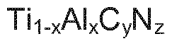
  • the present invention relates to a tool having a base body of cemented carbide, cermet, ceramics, steel or high-speed steel and a single-layer or multi-layer wear protection coating deposited thereon in the CVD process and having a thickness within the range of from 2 ⁇ to 25 ⁇ , wherein the wear protection coating comprises at least a Ti 1-x Al x C y N z layer with 0.40 ⁇ x ⁇ 0.95, 0 ⁇ y ⁇ 0.10 and 0.85 ⁇ z ⁇ 1 .15 having a thickness in the range of from 1 ⁇ to 16 ⁇ and having >85 vol-% face-centered cubic (fee) crystal structure.
  • the present invention further relates to a process for the production of the inventive tool.
  • Tools for the chip forming metal machining consist of a substrate body of cemented carbide, cermet, ceramics, steel or high-speed steel which in the most cases is provided with a single-layer or multi-layer hard material coating for the improvement of the cutting properties and/or the wear properties.
  • the hard material coating consists of layers of mono-metallic or mixed-metallic hard material phases. Examples of mono-metallic hard material phases are TiN, TiC, TiCN, AIN and AI2O 3 . Examples of mixed-metallic phases, wherein within one crystal a metal is in part replaced by another one, are TiAIN and TiAICN. Coatings of the afore-mentioned type are deposited by CVD processes (chemical vapor deposition), PCVD processes (plasma-enhanced CVD processes) or by PVD processes (physical vapor deposition).
  • residual stresses due to the manufacturing process and/or of mechanical, thermal and/or chemical treatment.
  • residual stresses for example between the coating and the substrate and between the individual layers of the coating, respectively, result from the different coefficients of thermal expansion of the materials.
  • the residual stresses can be tensile stresses or compressive stresses.
  • coatings deposited by PVD processes in general, there exist residual compressive stresses due to, amongst other reasons, the ion bombardment in this process.
  • CVD processes usually generate residual tensile stresses in the coating.
  • macro-stresses that are almost homogenously distributed across macroscopical regions of the material
  • micro-stresses that are homogenous within microscopic regions, such as for example within a grain
  • inhomogeneous micro-stresses that are inhomogeneous even at a microscopic level.
  • the residual stresses in hard material coatings can have a significant influence on the properties of the coatings with advantageous or disadvantageous effects on the wear resistance of the tool.
  • Residual tensile stresses exceeding the tension limit of the respective material can cause fractures and cracks in the coating perpendicular to the direction of the residual tensile stress.
  • a particular amount of residual compressive stress in the coating is desired, because it avoids and closes surface cracks and improves the fatigue properties of the coating and thereby of the tool.
  • too high residual compressive stresses can lead to adhesion problems and to chipping of the coating.
  • a mechanical surface treatment To increase the residual compressive stresses in the hard material coating of a tool, especially in hard material coatings deposited in the CVD process, it is known to subject the tool to a mechanical surface treatment.
  • Known mechanical treatment methods are the treatment by brushing and dry blasting or wet blasting. In the blasting treatment a fine grained blasting medium is directed onto the surface of the coating using compressed air under increased pressure.
  • Such a surface treatment can reduce residual tensile stresses and increase residual compressive stresses in the outermost layer, but also in the layers of the hard material coating arranged thereunder.
  • Single-layer or multi-layer wear protective coatings of tools for the chip forming metal machining often comprise one or more polycrystalline TiAIN and/or TiAICN layers having predominantly face-centered cubic crystal structure (fcc-TiAIN, fcc-TiAICN).
  • fcc-TiAIN layers have proven of value for the wear protection of tools for multiple chip forming applications.
  • fcc-TiAIN and fcc-TiAICN layers are characterized by the advantageous combination of increased hardness and oxidation resistance.
  • Fcc-TiAIN and fcc-TiAICN layers are thermodynamically metastable. It is known that fcc-TiAIN deposited by PVD processes decomposes at increased temperature first by spinodal decomposition into Al-rich and Ti-rich domains of fee- AIN and fcc-TiN, respectively. This goes along with an increase of the hardness and is known as "age hardening effect". When the temperature is further increased, the layer decomposes into the thermodynamically stable phases w-AIN (AIN having wurtzite structure) and fcc-TiN. For example, P.H.
  • the object of the present invention was to provide coated tools for the chip forming metal machin- ing, particularly for turning and milling of steel or cast materials, which exhibit, compared to the prior art, improved wear resistance and improved comb crack resistance in dry machining, as well as under the use of coolant.
  • a tool having a base body of cemented carbide, cermet, ceramics, steel or high-speed steel and a single-layer or multi-layer wear protection coating deposited thereon in the CVD process and having a thickness within the range of from 2 ⁇ to 25 ⁇ , wherein the wear protection coating comprises at least a Ti,. x Al x C y N z layer with 0.40 ⁇ x ⁇ 0.95, 0 ⁇ y ⁇ 0.10 and 0.85 ⁇ z ⁇ 1 .15 having a thickness in the range of from 1 m to 16 pm and having >85 vol-% face-centered cubic (fee) crystal structure, wherein the tool is characterized in that the T .
  • x Al x C y N z layer comprises precipitations of Ti"i. 0 AI 0 C p N q at the grain boundaries of the Tii. x Al x C y N z crystallites having a higher Al content than inside the crystallites, wherein 0.95 ⁇ o ⁇ 1 .00, 0 ⁇ p ⁇ 0.10, 0.85 ⁇ q ⁇ 1 .15 and (0-x) ⁇ 0.05.
  • . x Al x C y N z layer of the inventive stoichiometry that is deposited in the CVD process on a substrate body, usually exhibits residual tensile stresses after its deposition, as it is the case in most of the hard material layers produced in the CVD process.
  • Tools for the chip forming metal machining having such a layer in the wear protection coating are therefore subject to wear through crack formation, particularly comb crack formation.
  • the inventive tool which is produced as it will subsequently be described, in the Tii. x Al x C y N z layer, because of the precipitations at the grain boundaries, there is generated a residual stress condition, advantageously residual compressive stresses, leading to an improvement of the wear resistance and crack resistance, especially comb crack resistance.
  • . 0 AI 0 CpN q precipitations lies, starting from the surface of the Ti,. x Al x C y N z crystallites, in the range of about 4 nm to 200 nm, preferably 10 nm to 100 nm, par- ticularly preferably 25 nm to 75 nm. If the average thickness of the Ti"i. 0 AI 0 C p N q precipitations is too low, the increase of the residual compressive stresses in the Tii_ x Al x C y N z layer may be too low to achieve the herein described inventive advantages of improved wear resistance and crack resistance.
  • the total amount of precipitations is high. Because the precipitations contain a high proportion of hexagonal w-AIN, which is softer than the face-centered cubic Tii_ x Al x C y N z , a too high proportion of precipitations leads to an undesired decrease of the hardness of the layer and to impaired cutting properties.
  • inventive precipitations can, for example, be shown in the scanning transmission electron microscope (STEM) on sufficiently thin electron-transparent polished cross-sections of the coat- ings, preferably through lamellae prepared by focused ion beam (FIB), and their thickness can be determined using the STEM images.
  • STEM scanning transmission electron microscope
  • FIB focused ion beam
  • HAADF detectors High Angle Annular Dark Field detectors
  • the precipitations are made visible in the inverse contrast of the BF-image (bright field) and the HAADF-image.
  • the ⁇ 1-0 ⁇ 0 ⁇ ⁇ ⁇ ⁇ ⁇ precipitations having a higher Al content than inside the crystallites appear brighter than the Ti 1-x Al x C y N z crystallites in the BF-image, and in the HAADF-image the Ti"i. 0 AI 0 C p N q precipitations appear darker than the T . x Al x C y N z crystallites.
  • HRTEM transmission electron microscopy
  • x Al x C y N z crystallite as well as from regions of the Ti-
  • index- ing of the diffraction images one can show that the face-centered cubic (fee) phase is present in the Tii_ x Al x C y N z crystallite, that the crystalline domains of the Tii. 0 AI 0 C p N q grain boundary precipitations have the w-AIN structure, and that there exist epitaxial relationships between the fee T . x Al x C y N z crystallites and the w-AIN precipitation.
  • precipitations can be made visible in the scanning electron microscope (SEM) in embedded metallographic polished cross-sections or in samples polished parallel to the surface.
  • SEM scanning electron microscope
  • the produced tool is separated, embedded and then treated in the following manner: 6 min of grinding using a grinding wheel Struers Piano220 and water; 3 min of polishing using Struers 9 ⁇ MD-Largo diamond suspension; 3:40 min of polishing using Struers 3 ⁇ MD-Dac diamond suspension; 2 min of polishing using Struers 1 ⁇ MD-Nap diamond suspension; at least 12 min of chemical polishing using Struers OP-S (suspension of colloidal silicone dioxide having an average particle size of 0,04 ⁇ ). Prior to the subsequent SEM examination the samples are cleaned in an ultrasonic bath and demagnetized. On the so produced polished cross-sections the inventive Tii.
  • x Al x C y N z layer EBSD measurements were carried out on the prepared polished cross-sections.
  • a FE-SEM Zeiss Supra 40 VP
  • an EBSD detector ED AX Digiview
  • the electron beam was recorded in "High Current" mode in a hexagonal pattern applying sufficiently small increments (typically 0.03-0.04 ⁇ ; at least 5 times smaller than the average crystallite broadness evaluated from SEM images) at an accelerating voltage of 15 kV, 70° tilt and application of 60 ⁇ or 120 ⁇ apertures.
  • the EBSD map is cropped using the "crop" function in a way that only data points of the Ti-
  • the remaining maps still represent at least 50%, usually >75% of the thickness of the Ti-
  • a CI standardization (“grain CI standardization”) is carried out applying a tolerance angle (“grain tolerance angle”) of 5° and a minimum grain size of 5 data points.
  • partitioning of the so generated data set is carried out applying the filter Cl>0.1 , i.e. all data points that, after CI standardization, have a lower confidence index are disregarded.
  • the described method of the EBSD measurement does not provide information about the phase and orientation of those proportions of the Ti -x Al x C y N z layers that are at close range (distance of about ⁇ 50 nm) to the grain boundaries, and phase and orientation of the inventive Ti-
  • the method reliably detects the face-centered cubic (fee) phase present in the crystallites of the Ti 1-x Al x C y N z layer and thus provides a value of the minimum content of fee phase in the Tii. x Al x C y N z layer.
  • the thickness or the volume proportion, respectively, of the inventive precipitations can be varied during the preparation of the inventive Tii. x Al x C y N z layer, especially by the duration and temperature of the annealing, according to the process for the preparation of the inventive tool, as it will subsequently be described in detail.
  • the skilled person can, if he knows the present invention, determine the suitable parameters of duration and temperature within the inventive ranges for a desired precipitation thickness or precipitation volume proportions, respectively, by only a few experiments.
  • the inventive Ti 1-x Al x C y N z layer has predominantly face-centered cubic (fee) crystal structure.
  • proportions of softer other phases such as for example hexagonal AIN, can be present in the layer, which, however, are undesired if they are formed by co-deposition together with the fcc-Ti 1-x Al x C y N z structure, because they disadvantageously influence the hardness and the wear resistance.
  • the Ti -x Al x C y N z layer of the inventive tool comprises at least 90 vol.%, preferably at least 95 vol%, particularly preferably at least 98 vol% of face-centered cubic (fee) crystal structure.
  • face-centered cubic (fee) crystal struc- ture is in the Ti-
  • x Al x C y N z layer the higher is the wear resistance.
  • the Ti 1-x Al x C y N z layer has a columnar micro- structure.
  • Polycrystalline hard material layers of TiAICN and/or TiAIN produced in the CVD process can, except for columnar microstructure, also exhibit rather equiaxed microstructures.
  • the Ti 1-x Al x C y N z layer having columnar microstructure has the advantage that during the formation of Ti-
  • equiaxed structures in general, less pro- nounced growth textures than in columnar structures are formed so that a ⁇ 1 1 1 ⁇ fibre texture, which is desired according to a preferred embodiment of the invention, cannot form.
  • the Ti 1-x Al x C y N z layer comprises essentially no carbide carbon, except for unavoidable impurities and/or impurities conditional of manufacturing.
  • This essentially pure nitride layer has the advantage of a simpler process control during the CVD coating. Furthermore, a more homogenous control of the layer properties and the layer composition within one coating batch is facilitated.
  • . x Al x C y N z layer has a Vickers hard- ness (HV) of more than 2700 HV, preferably more than 3000 HV, particular preferably more than 3200 HV.
  • HV Vickers hard- ness
  • a too low Vickers hardness has the disadvantage of unfavorable cutting properties and too low wear resistance.
  • the high Vickers hardness is achieved by the application of the inventive process for the production of the tool that will subsequently be described in more detail. If during the annealing of the Tii. x Al x C y N z layer a too high temperature and/or a too long time of annealing is applied, the Vickers hardness of the Ti 1 .
  • the Ti 1-x Al x C y N z layer has a preferred orientation of the crystal growth with respect to the crystallographic ⁇ 1 1 1 ⁇ plane. This is characterized by a texture coefficient TC (1 1 1 ) > 1 .5, preferably > 2. particularly preferably > 3.
  • TC (1 1 1 ) > 1 .5, preferably > 2, particularly preferably > 3 has turned out to be particularly advantageous.
  • TC (1 1 1 ) > 1 .5, preferably > 2, particularly preferably > 3 has turned out to be particularly advantageous.
  • TC (1 1 1 1 ) > 1 .5, preferably > 2, particularly preferably > 3 has turned out to be particularly advantageous.
  • TC (1 1 1 ) > 1 .5, preferably > 2, particularly preferably > 3 has turned out to be particularly advantageous.
  • TC (1 1 1 ) > 1 .5, preferably > 2, particularly preferably > 3 has turned out to be particularly advantageous.
  • TC (1 1 1 ) > 1 .5, preferably > 2, particularly preferably > 3 has turned out to be particularly advantageous.
  • XRD X-ray diffraction
  • EBSD electron back scattering
  • the half width (FWHM) of the X-ray diffraction peak of the crystallographic ⁇ 1 1 1 ⁇ plane is ⁇ 2 ⁇ , preferably ⁇ 0.6° 2 ⁇ , particularly preferably ⁇ 0.45° 2 ⁇ .
  • a too high half width (FWHM) of the X-ray diffraction peak of the ⁇ 1 1 1 ⁇ plane of the Ti 1-x Al x CyN z is an indication of lower grain sizes of the face-centered cubic (fee) phase or even of proportions of amorphous phases. In the tests carried out so far this has shown to be disadvantageous for the wear resistance.
  • the inventive lamellar structure provides for good service lives of the tool in cutting operations.
  • the service lives are also significantly higher than for lamellar TiAIN or TiAICN structures that are known from the prior art and having alternating crystal structures, namely alternating face-centered cubic and hexagonal crystal structures of the lamellae.
  • the T . x Al x C y N z layer has residual com- pressive stresses, preferably within the range of from ⁇ 0 MPa to -5000 MPa, particularly preferably within the range of from -300 MPa to -3500 MPa, measured on the ⁇ 222 ⁇ reflection at « 81 .5 - 82 degrees 2-theta of the fcc-Tii -x Al x C y N z phase by the ⁇ 2 ⁇ method.
  • At least one further hard material layer with a thickness of from 0.05 pm to 7 ⁇ , preferably of from 0.1 ⁇ to 5 ⁇ , particularly preferably of from 0.2 ⁇ to 3 ⁇ , selected from a TiN layer, a TiCN layer deposited by high-temperature CVD or mod erate-tem peratu re CVD (MT-CVD), a Al 2 0 3 layer, a h-AIN layer and combinations thereof. Furthermore, it is preferred if above the Ti-i.
  • At least one further hard material layer preferably selected from (/.-AI2O 3 , K-AI2O 3 , Y-AI2O 3 , TiN, T-TiCN, h-AIN and combinations thereof.
  • Particularly preferred is a ⁇ - ⁇ 2 0 3 layer, wherein the Al 2 0 3 layer is deposit- ed by high-temperature CVD (CVD) or moderate-temperature CVD (MT-CVD).
  • the invention also relates to a process for the production of the herein described inventive tool having a base body of cemented carbide, cermet, ceramics, steel or high-speed steel and a single-layer or multi-layer wear protection coating deposited thereon by the CVD process and having a thickness within the range of from 2 ⁇ to 25 ⁇ , wherein the process comprises the following steps:
  • x Al x C y N z layer has a Vickers hardness (HV) of more than 2700 HV, preferably more than 3000 HV, particularly preferably more than 3200 HV.
  • HV Vickers hardness
  • Temperature and duration during annealing are selected in a way that not too much of hexagonal AIN phase is precipitated and the hardness of the Ti 1 .
  • x Al x C y N z layer does not drop below the preferred values. Therefore, at high temperatures, a shorter duration of annealing has to be selected, and vice versa.
  • the enclosed figure 4 shows examples of the development of hardness at different annealing temperatures and different durations, herein 3 h or 5 h, respectively.
  • the conditions of temperature and duration during annealing are selected in a way that the remaining content of face-centered cubic (fee) crystal structure in the Ti 1-x Al x C y N z layer, after the generation of the precipitations of Tii_ o Al o C p q in the Ti -x Al x C y N z layer after the annealing, is > 85 vol%.
  • a Ti-i is a Ti-i.
  • the inventive process after the as such known deposition of the Tii -x Al x C y N z layer, there follows an annealing treatment wherein the inventive precipitations are generated. Thereby, it is essential that the annealing is carried out at a temperature within the range of from 700 - 950 °for a duration of 0.5 - 12 hours under exclusion of air or oxygen, respectively.
  • the annealing can be carried out after the deposition of the Tii -x Al x C y N z layer and of the optional further layers of the coating in a separate process and/or in a different reactor than the deposition of the hard material layers. But the annealing can also be carried out immediately following the deposition of the Ti 1-x Al x C y N z layer in the same reactor. It can, for example, be a part of the subsequent deposition of one or more further hard material layers above the Ti"i. x Al x C y N z layer by CVD. Thereby, it has to be considered that the subsequent deposition process or processes is/are carried out at temperatures and for durations below the upper limits defined herein for the inventive process.
  • Thermal CVD processes using temperatures above 950 °C are therefore not suitable, whereas, for example, MT-CVD processes are generally carried out at about 700 - 900°C and are thus within the temperature range of the inventive process.
  • tools of the inventive type exhibit significantly higher wear resistance, especially resistance against flank wear, as well as significantly higher resistance against crack formation, especially comb crack formation, than non-annealed tools and than tools that are annealed out- side the process parameters that are essential to the present invention, especially at too high temperature.
  • the annealing of the deposited T _ x Al x C y N z layer is carried out at a temperature within the range of from 750 - 900 °C, preferably 800 - 850 °C and/or for a duration of from 1 -6 hours.
  • An essential process condition is also the exclusion of air, because otherwise the Ti -x Al x CyN z layer may oxidize.
  • the process can. for example, be carried out under vacuum or protective gas atmosphere, such as argon, hydrogen or nitrogen.
  • the precipitations formed in the inventive process at the grain boundaries generate in the Ti-i. x Al x C y N z layer a residual stress condition, advantageously residual compressive stresses, resulting in an improvement of the wear resistance and resistance against crack formation, especially resistance against comb crack formation.
  • . x Al x C y N z layer is a LP-CVD process (low pressure CVD process), which is carried out at a process pressure within the CVD reactor within the range of from 0.05 to 8 kPa, preferably within the range of from 0.1 to 7 kPa, particularly preferably within the range of from 0.3 to 2 kPa.
  • LP-CVD process low pressure CVD process
  • . x Al x C y N z layer is a LP-CVD process (low pressure CVD process), which is carried out at a process pressure within the CVD reactor within the range of from 0.05 to 8 kPa, preferably within the range of from 0.1 to 7 kPa, particularly preferably within the range of from 0.3 to 2 kPa.
  • At higher process pressures general- ly, no Tii -x Al x C y N z layers having face-
  • EBSD analysis was performed using a Digiview IV detector from Ametek EDAX in a Supra 40 VP FE-SEM from Carl Zeiss. The recoding conditions and the evaluation processes for EBSD are described above in more detail.
  • a transmission electron microscope FEI Titan 80-300 with field emission cathode at an acceleration voltage of 300 kV was used. Scanning transmission electron microscope images were taken using Bright Field (BF; Bright Field) and High Angle Annular Dark Field- (HAADF) detectors.
  • BF Bright Field
  • HAADF High Angle Annular Dark Field-
  • FIB Focused Ion Beam
  • EDX measurements were carried out on a scanning electron microscope Supra 40 VP from Carl Zeiss at 15 kV acceleration voltage with an EDX spectrometer of the type INCA x-act from Oxford Instruments, UK.
  • EDX measurements on the transmission electron microscope Titan 80-300 80-300 TEM/STEM there was also used an Inca EDX System from Oxford Instruments, UK.
  • X-ray diffraction measurements were done on a diffractometer of the type GE Sensing & Inspec- tion Technologies PTS3003 using CuKa-radiation.
  • a parallel beam optics was used consisting on the primary side of a polycapillary and a 2mm pinhole as collimator.
  • a parallel plate collimator with a divergence of 0.4° and a nickel Kp filter was used. Peak intensities and half widths were determined from ⁇ -2 ⁇ measurements.
  • pseudo-Voigt-functions were fitted to the measurement data, whereby the Ka 2 - subtraction was carried out by Ka 1 /Ka 2 -doublet fitting.
  • Peak intensities and half widths relate to the thus fitted Kc i interferences.
  • the lattice constants were calculated according to Vergard's law using the lattice constants of TiN and AIN from the pdf cards 38-1420 and 00-046-1200, respec- tively.
  • the intensity distribution of all measured and back-calculated pole figures was approximately rotationally symmetrical, i.e. the investigated layers exhibited fibre texture.
  • pole figures were measured on the ⁇ 200 ⁇ and ⁇ 220 ⁇ reflections.
  • the orientation density distribution function (ODF) was calculated using the software LaboTex3.0 from LaboSoft, Poland, and the preferential orientation was represented by an inverse pole figure.
  • ODF orientation density distribution function
  • the intensity maximum was in the crystallographic direction ⁇ 1 1 1 >, corresponding to the set preferential orientation or within an angle deviation of ⁇ 20° from ⁇ 1 1 1 >.
  • the ⁇ 222 ⁇ interference of the face-centered cubic T .xAlxCyNz layer was measured according to the ⁇ 2 ⁇ method applying 25 ⁇ angles from -60° to +60° (increment 5°) using the diffractometer GE Sensing & Inspection Technologies PTS3003 with the above-described measurement optics. After background subtraction, Lorentz-polarization correction and Kc/.2 subtraction (Rachinger separation), the positions of the lines of the interferences were determined by fitting of the profile functions to the measured data.
  • Residual stresses are generally indicated in the unit Megapascal (MPa), whereby residual tensile stresses are designated by a positive algebraic sign (+) and residual compressive stresses are designated by a negative algebraic sign (-).
  • micro-hardness and of the modulus of indentation were carried out accord- ing to DIN EN ISO 14577 using a universal hardness tester.
  • Fischerscope H100 from Helmut Fischer GmbH, Sindelfingen, Germany, on a polished cross-section of the coated body.
  • the measurements of the micro-hardness were carried out applying a test load of 25 mN.
  • Figure 1 shows a schematic representation of a hard material coating on a tool substrate 3 in cross-section.
  • a coating layer 2 deposited in the CVD process, which can for example be an adhesion layer of TiN.
  • x Al x C y N z layer 1 without inventive precipitations, as it is known from the prior art or as it can look like in the inventive process prior to the annealing.
  • the T . x Al x C y N z layer 1 has a columnar structure with crystallites 4 and grain boundaries 5.
  • Figure 2 shows a schematic representation of an inventive hard material coating similar to figure 1 , but with inventive precipitations 6 of Ti-
  • . 0 Ai 0 C p N q have a higher AIN content than inside the Tii. x Al x C y N z crystallites.
  • Figure 3 schematically shows a concentration profile of the stoichiometric Al proportion (x) in the Tii -x Al x C y N z layer across a grain boundary of two adjacent crystallites.
  • . x Al x C y N z crystallites to the grain boundary is constant.
  • the stoichiometrical Al proportion (x) starting from the inside of the adjacent Ti"i_ x Al x C y N z crystallites to the grain boundary, first decreases, but then it significantly increases at the grain boundary to above the Al proportion inside the adjacent Tii. x Al x C y N z crystallites.
  • Figure 4 shows the measured values of the micro-hardnesses of the non-annealed
  • non-annealed are to be assigned to the non-annealed tools.
  • the increase of the hardness was low at both holding times, however, the tools annealed according to the invention achieved significantly better results in the wear tests.
  • Figures 5, 6, 7 show the comb crack formation (figure 5), the maximum flank wear (figure 6) and the average flank wear (figure 7) of the tools 7 to 1 1 of the subsequent examples annealed for 5 h in the milling test over the milling path.
  • Example 1 Preparation of coated cemented carbide indexable cutting inserts and analysis As substrate bodies in these examples cemented carbide indexable cutting inserts of the geometry SEHW1204AFN having a composition of 90.5 wt-% WC, 8 wt-% Co and 1.5 wt-% (NbC+TaC) were used.
  • a first precursor gas mixture (VG1 ) containing the starting compounds TiCI 4 and AICI 3 and a second precursor gas mixture (VG2) containing the starting component NH 3 as reactive nitrogen component were introduced into the reactor separately so that a blending of the two gas streams took place not earlier than at the entry into the reaction zone.
  • the volume gas streams of the precursor gas mixtures (VG1 ) and (VG2) were set in a manner that a mean retention time r of the reaction gases in the reactor and a total volume stream under normal conditions ' ⁇ was achieved.
  • . x Al x C y N z layer are indicated in table 2.
  • the thickness of the Tiizie x Al x C y N z layer was about 8 ⁇ for cotaing #1 and about 6 ⁇ for coating #2.
  • XRD X-ray diffraction
  • EBSD scanning electron microscopy
  • STEM scanning transmission electron microscopy
  • TEM transmission electron microscopy
  • lamellar structures were visible in STEM images.
  • the lamellar structure of the inventive Ti 1-x Al x CyN z layers is characterized by inverse bright/dark-contrasts in the imaging modes bright field (BF) and "high angle annular dark field” (HAADF). This contrast inversion is an indication of different chemical compositions of the bright and dark regions of the lamellar structure. The regions appearing bright and dark have generally different thicknesses.

Landscapes

  • Chemical & Material Sciences (AREA)
  • Engineering & Computer Science (AREA)
  • Mechanical Engineering (AREA)
  • Chemical Kinetics & Catalysis (AREA)
  • Materials Engineering (AREA)
  • Metallurgy (AREA)
  • Organic Chemistry (AREA)
  • General Chemical & Material Sciences (AREA)
  • Inorganic Chemistry (AREA)
  • Cutting Tools, Boring Holders, And Turrets (AREA)
  • Chemical Vapour Deposition (AREA)

Abstract

Tool having a base body of cemented carbide, cermet, ceramics, steel or high-speed steel and a single-layer or multi-layer wear protection coating deposited thereon in the CVD process and having a thickness within the range of from 2 μm to 25 μm, wherein the wear protection coating comprises at least a Ti1-xAlxCyNz layer with 0.40 ≤ x ≤ 0.95, 0 ≤ y ≤ 0.10 and 0.85 ≤ z ≤ 1.15 having a thickness in the range of from 1 μm to 16 μm and having >85 vol-% face-centered cubic (fcc) crystal structure, wherein the Ti1-xAlxCyNz layer comprises precipitations of Ti1-oAIoCpNq at the grain boundaries of the Ti1-xAlxCyNz crystallites having a higher Al content than inside the crystallites, wherein 0.95≤o≤1.00, 0≤p≤0.10, 0.85≤q≤1.15 and (0-x)≥0.05.

Description

TOOL WITH TIALN COATING
FIELD OF THE INVENTION
The present invention relates to a tool having a base body of cemented carbide, cermet, ceramics, steel or high-speed steel and a single-layer or multi-layer wear protection coating deposited thereon in the CVD process and having a thickness within the range of from 2 μιτι to 25 μιη, wherein the wear protection coating comprises at least a Ti1-xAlxCyNz layer with 0.40≤ x≤ 0.95, 0≤ y≤ 0.10 and 0.85≤ z≤ 1 .15 having a thickness in the range of from 1 μιτι to 16 μιη and having >85 vol-% face-centered cubic (fee) crystal structure. The present invention further relates to a process for the production of the inventive tool.
BACKGROUND OF THE INVENTION
Tools for the chip forming metal machining consist of a substrate body of cemented carbide, cermet, ceramics, steel or high-speed steel which in the most cases is provided with a single-layer or multi-layer hard material coating for the improvement of the cutting properties and/or the wear properties. The hard material coating consists of layers of mono-metallic or mixed-metallic hard material phases. Examples of mono-metallic hard material phases are TiN, TiC, TiCN, AIN and AI2O3. Examples of mixed-metallic phases, wherein within one crystal a metal is in part replaced by another one, are TiAIN and TiAICN. Coatings of the afore-mentioned type are deposited by CVD processes (chemical vapor deposition), PCVD processes (plasma-enhanced CVD processes) or by PVD processes (physical vapor deposition).
In almost every material there are residual stresses due to the manufacturing process and/or of mechanical, thermal and/or chemical treatment. During the production of tools by coating of a substrate body by CVD processes, residual stresses, for example between the coating and the substrate and between the individual layers of the coating, respectively, result from the different coefficients of thermal expansion of the materials. The residual stresses can be tensile stresses or compressive stresses. In coatings deposited by PVD processes, in general, there exist residual compressive stresses due to, amongst other reasons, the ion bombardment in this process. In contrast to that, CVD processes usually generate residual tensile stresses in the coating.
There is distinguished between three types of residual stresses: macro-stresses that are almost homogenously distributed across macroscopical regions of the material, micro-stresses that are homogenous within microscopic regions, such as for example within a grain, and inhomogeneous micro-stresses that are inhomogeneous even at a microscopic level. From a practical point of view and for the mechanical properties of a cutting tool the macro-stresses are of particular importance. The residual stresses in hard material coatings can have a significant influence on the properties of the coatings with advantageous or disadvantageous effects on the wear resistance of the tool. Residual tensile stresses exceeding the tension limit of the respective material can cause fractures and cracks in the coating perpendicular to the direction of the residual tensile stress. In general, a particular amount of residual compressive stress in the coating is desired, because it avoids and closes surface cracks and improves the fatigue properties of the coating and thereby of the tool. However, too high residual compressive stresses can lead to adhesion problems and to chipping of the coating.
To increase the residual compressive stresses in the hard material coating of a tool, especially in hard material coatings deposited in the CVD process, it is known to subject the tool to a mechanical surface treatment. Known mechanical treatment methods are the treatment by brushing and dry blasting or wet blasting. In the blasting treatment a fine grained blasting medium is directed onto the surface of the coating using compressed air under increased pressure. Such a surface treatment can reduce residual tensile stresses and increase residual compressive stresses in the outermost layer, but also in the layers of the hard material coating arranged thereunder.
Single-layer or multi-layer wear protective coatings of tools for the chip forming metal machining often comprise one or more polycrystalline TiAIN and/or TiAICN layers having predominantly face-centered cubic crystal structure (fcc-TiAIN, fcc-TiAICN). Especially fcc-TiAIN layers have proven of value for the wear protection of tools for multiple chip forming applications. Compared to the monometallic border systems of the hard material phases fcc-TiN, fcc-TiCN or AIN having hexagonal structure (w-AIN), fcc-TiAIN and fcc-TiAICN layers are characterized by the advantageous combination of increased hardness and oxidation resistance. Fcc-TiAIN and fcc-TiAICN layers are thermodynamically metastable. It is known that fcc-TiAIN deposited by PVD processes decomposes at increased temperature first by spinodal decomposition into Al-rich and Ti-rich domains of fee- AIN and fcc-TiN, respectively. This goes along with an increase of the hardness and is known as "age hardening effect". When the temperature is further increased, the layer decomposes into the thermodynamically stable phases w-AIN (AIN having wurtzite structure) and fcc-TiN. For example, P.H. ayrhofer et al., Applied Physics Letters, 83/10 (2003), pages 2049- 2051 , report about a spinodal decomposition of a Tio.5Alo.5N layer, which is deposited in the PVD process, at 860°C beginning from the bulk of the coating material. The hardness of the coating decreases beginning at about 850°C, and above about 950°C it is lower than in the non-annealed state. Adibi et al., J. Appl. Phys., 69/9 (1991 ), pages 6437-6450 report about the PVD deposition of Tio.5Alo.5N coatings, wherein a surface-initiated spinodal decomposition is observed in a temperature range of 540-560'C and at a further increase of the temperature a phase separation into fcc-TiN and w-AIN is observed. Significant proportions of w-AIN phase, which is softer than fcc-TiAIN and fcc-TiN phases, lead to unfavorable mechanical and tribological properties of the coating. The phase conversion is promoted by stacking faults.
OBJECT OF THE INVENTION
The object of the present invention was to provide coated tools for the chip forming metal machin- ing, particularly for turning and milling of steel or cast materials, which exhibit, compared to the prior art, improved wear resistance and improved comb crack resistance in dry machining, as well as under the use of coolant.
DESCRIPTION OF THE INVENTION
This object is solved by a tool having a base body of cemented carbide, cermet, ceramics, steel or high-speed steel and a single-layer or multi-layer wear protection coating deposited thereon in the CVD process and having a thickness within the range of from 2 μπι to 25 μιτι, wherein the wear protection coating comprises at least a Ti,.xAlxCyNz layer with 0.40≤ x≤ 0.95, 0≤ y≤ 0.10 and 0.85≤ z < 1 .15 having a thickness in the range of from 1 m to 16 pm and having >85 vol-% face-centered cubic (fee) crystal structure, wherein the tool is characterized in that the T . xAlxCyNz layer comprises precipitations of Ti"i.0AI0CpNq at the grain boundaries of the Tii.xAlxCyNz crystallites having a higher Al content than inside the crystallites, wherein 0.95≤o≤1 .00, 0≤p≤0.10, 0.85<q≤1 .15 and (0-x)≥0.05.
A Ti-|.xAlxCyNz layer of the inventive stoichiometry, that is deposited in the CVD process on a substrate body, usually exhibits residual tensile stresses after its deposition, as it is the case in most of the hard material layers produced in the CVD process. Tools for the chip forming metal machining having such a layer in the wear protection coating are therefore subject to wear through crack formation, particularly comb crack formation. In the inventive tool, which is produced as it will subsequently be described, in the Tii.xAlxCyNz layer, because of the precipitations at the grain boundaries, there is generated a residual stress condition, advantageously residual compressive stresses, leading to an improvement of the wear resistance and crack resistance, especially comb crack resistance. This could be proved by experiments comparing coated tools having the same layer sequence and comprising a T .xAlxCyNz wear protection layer without or with the inventive precipitations at the grain boundaries. Compared to the comparative tools, in milling tests the inventive tools exhibited longer service lives, less comb crack formation and high thermal stability of the Ti1-xAlxCyNz wear protection layer. The inventive precipitations of Ti-i_0AI0CpNq having a higher Al content than inside the Ti-i.xAlxCyNz crystallites are generated during the production of the tool according to the inventive process, which will subsequently be described in more detail. Without being bound to a theory, the inven- tors assume that the precipitations of Ti-|.0AI0CpNq essentially consist of AIN having the hexagonal wurtzite structure (w-AIN), wherein the precipitations can contain low proportions of Ti and C. It is assumed that during the generation of the precipitations from the Tii.xAlxCyNz crystallites having face-centered cubic crystal structure a phase conversion into the hexagonal phase takes place. The hexagonal w-AIN phase could be verified in the precipitations. Furthermore, the analytical results suggest that there are epitaxial relationships between the w-AIN grain boundary precipitations and each of the adjacent fee- Tii-xAlxCyNz crystallites. Because the hexagonal w-AIN phase has a higher volume than the face-centered cubic phase, the conversion apparently goes along with an expansion of the volume. It is therefore further assumed that this expansion of the volume at the grain boundaries of the Ti1-xAlxCyNz crystallites leads to an increase of the residual com- pressive stress in the Tii„xAlxCyNz layer, which in turn results in an improvement of the wear resistance and the crack resistance, especially the comb crack resistance.
The average thickness of the Ti-|.0AI0CpNq precipitations lies, starting from the surface of the Ti,.xAlxCyNz crystallites, in the range of about 4 nm to 200 nm, preferably 10 nm to 100 nm, par- ticularly preferably 25 nm to 75 nm. If the average thickness of the Ti"i.0AI0CpNq precipitations is too low, the increase of the residual compressive stresses in the Tii_xAlxCyNz layer may be too low to achieve the herein described inventive advantages of improved wear resistance and crack resistance. If the Ti-i„0AI0CpNq precipitations have a too high thickness, then the total amount of precipitations is high. Because the precipitations contain a high proportion of hexagonal w-AIN, which is softer than the face-centered cubic Tii_xAlxCyNz, a too high proportion of precipitations leads to an undesired decrease of the hardness of the layer and to impaired cutting properties.
The inventive precipitations can, for example, be shown in the scanning transmission electron microscope (STEM) on sufficiently thin electron-transparent polished cross-sections of the coat- ings, preferably through lamellae prepared by focused ion beam (FIB), and their thickness can be determined using the STEM images. Preferably, HAADF detectors (High Angle Annular Dark Field detectors) are used, and the precipitations are made visible in the inverse contrast of the BF-image (bright field) and the HAADF-image. Thereby, the Τί1-0ΑΙ0ΟρΝς precipitations having a higher Al content than inside the crystallites appear brighter than the Ti1-xAlxCyNz crystallites in the BF-image, and in the HAADF-image the Ti"i.0AI0CpNq precipitations appear darker than the T . xAlxCyNz crystallites. At a suitable sample thickness and orientation of the Ti1-xAlxCyNz crystallite relative to the electron beam, by high-resolution transmission electron microscopy (HRTEM) one can obtain images from which diffraction images from the Ti-|.xAlxCyNz crystallite, as well as from regions of the Ti-|.0AI0CpNq excretion at the grain boundary can be derived by Fourier-transformation. By index- ing of the diffraction images one can show that the face-centered cubic (fee) phase is present in the Tii_xAlxCyNz crystallite, that the crystalline domains of the Tii.0AI0CpNq grain boundary precipitations have the w-AIN structure, and that there exist epitaxial relationships between the fee T . xAlxCyNz crystallites and the w-AIN precipitation. In an alternative, precipitations can be made visible in the scanning electron microscope (SEM) in embedded metallographic polished cross-sections or in samples polished parallel to the surface. Thereby, one takes advantage of the effect that in the final polishing step of the subsequently described preparation process w-AIN is stronger etched than the regions of cubic phases. Since the inventive precipitations contain a high proportion of hexagonal w-AIN, they are clearly visible in the prepared polished cross-sections.
For the preparation of a polished cross-section for the described analyses the produced tool is separated, embedded and then treated in the following manner: 6 min of grinding using a grinding wheel Struers Piano220 and water; 3 min of polishing using Struers 9 μιτι MD-Largo diamond suspension; 3:40 min of polishing using Struers 3 μιτι MD-Dac diamond suspension; 2 min of polishing using Struers 1 μιτι MD-Nap diamond suspension; at least 12 min of chemical polishing using Struers OP-S (suspension of colloidal silicone dioxide having an average particle size of 0,04 μιτι). Prior to the subsequent SEM examination the samples are cleaned in an ultrasonic bath and demagnetized. On the so produced polished cross-sections the inventive Tii.xAlxCyNz layers are imaged in the FE-SEM using a secondary electron detector at an accelerating voltage of 2.5 kV and typical working distances of 3-10 mm. Thereby, in the polished cross-section of the inventive samples there is observed the columnar structure of the Ti1-xAlxCyNz layer, which in the non- annealed condition has about 100% face-centered cubic (fee) structure. The inventive precipitations at the grain boundaries, that are etched stronger than the crystallites in the final step of chemical polishing in the above-described preparation, can be identified as darker regions due to the topography and the atomic number contrast. From the complementary XRD and EBSD results, as well as from comparative examinations on polished cross-sections of non-annealed T . xAlxCyNz layers and pure w-AIN layers one can conclude that the crystallites contain essentially 100% face-centered cubic phase, whereas the w-AIN phase proportions formed through the annealing are contained in the Tii-0AI0CpNq grain boundary precipitations, whereby it is supposed that the Tii-0AI0CpNq grain boundary precipitations predominantly consist of w-AIN. The determi- nation of the broadness of the Ti1-0AI0CPNq grain boundary precipitations and the determination of the minimum content of fee phase in the inventive Tii.xAlxCyNz layer is generally possible on the so generated images by measuring the images or by the application of established image analysis procedures.
For the determination of the minimum content of fee phase in the inventive Ti-|.xAlxCyNz layer EBSD measurements were carried out on the prepared polished cross-sections. For the examination of the layers produced in the examples a FE-SEM (Zeiss Supra 40 VP) with an EBSD detector (ED AX Digiview) was used. For the recording of the EBSD diffraction pattern, the electron beam was recorded in "High Current" mode in a hexagonal pattern applying sufficiently small increments (typically 0.03-0.04 μιτι; at least 5 times smaller than the average crystallite broadness evaluated from SEM images) at an accelerating voltage of 15 kV, 70° tilt and application of 60 μιτι or 120 μιτι apertures. The data analysis of the EBSD maps using the OIM Analysis 7 software from Ametek EDAX was carried out as follows: In the first step, the EBSD map is cropped using the "crop" function in a way that only data points of the Ti-|.xAlxCyNz layer remain in the data set and that regions at the upper and lower borders, where due to the preparation process the polish is not plane, are also cropped. When applying the described preparation process, the remaining maps still represent at least 50%, usually >75% of the thickness of the Ti-|.xAlxCyNz layer. In the second step, a CI standardization ("grain CI standardization") is carried out applying a tolerance angle ("grain tolerance angle") of 5° and a minimum grain size of 5 data points. In the third step, partitioning of the so generated data set is carried out applying the filter Cl>0.1 , i.e. all data points that, after CI standardization, have a lower confidence index are disregarded.
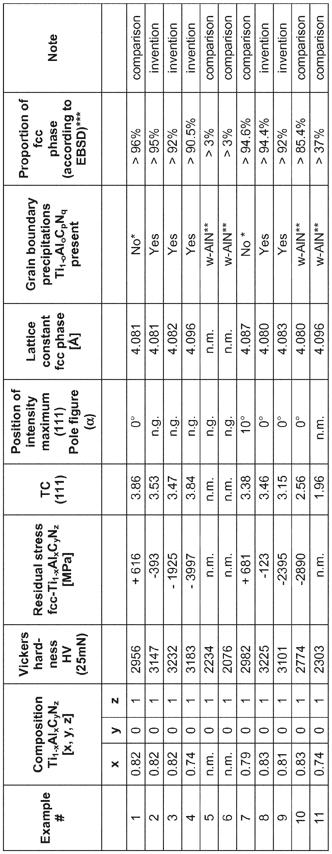
On comparative samples of non-annealed Ti-|.xAlxCyNz layers, consisting essentially 100% of face-centered cubic (fee) phase, i.e. wherein no signals of w-AIN are visible in the X-ray diffracto- gram and wherein in the SEM on a polished cross-section no etching effect resulting from the preparation is visible at the grain boundaries, by this type of EBSD measurement and analysis typically >95% of the data points of the cropped map are indexed as fee phase, significantly less than 1 % as w-AIN, and the rest with C 0.1 is neglected. Since through the described complementary analysis procedures it was determined that the sample consists of approximately 100% fee phase, one can conclude that the very low proportion of "w-AIN" data points must be a result of mis-indexing by the software. For the neglected data points with C 0.1 one can assume that at these measurement points fee phase is actually present. These data points predominantly lie at the grain boundaries where at lateral distances of the measurement point from the grain boundary below a few nm a superposition of diffraction images of adjacent grains can occur. In addition, through orientation-dependent etching there can occur height differences between adjacent grains. Both effects make that close to the grain boundaries diffraction images of relatively bad quality appear and that an indexing of the phase and orientation cannot securely be made by the software. Thus, the described method of the EBSD measurement does not provide information about the phase and orientation of those proportions of the Ti -xAlxCyNz layers that are at close range (distance of about < 50 nm) to the grain boundaries, and phase and orientation of the inventive Ti-|.0AI0CpNq grain boundary precipitations are not detected because of the too low grain size and the morphology generated by the preparation. However, the method reliably detects the face-centered cubic (fee) phase present in the crystallites of the Ti1-xAlxCyNz layer and thus provides a value of the minimum content of fee phase in the Tii.xAlxCyNz layer. Thereby, for non- annealed Tii_xAlxCyNz layers having an actual content of about 100% fee phase, typical values of >95% area proportion of fee phase are obtained. An annealed sample having Tii-0AI0CpNq grain boundary precipitations the minimum proportions of the fee phase determined by EBSD are to some percent lower, and from the difference compared to the measured minimum proportion of fee phase in the non-annealed comparative sample one can estimate the volume proportion of the formed grain boundary precipitations. The measurement results of the produced coatings of the examples, as listed in table 4, show that the Ti"i.0AI0CpNq grain boundary precipitations in the inventive Tii.xAlxCyNz layers make up a volume proportion of below 10%.
The thickness or the volume proportion, respectively, of the inventive precipitations can be varied during the preparation of the inventive Tii.xAlxCyNz layer, especially by the duration and temperature of the annealing, according to the process for the preparation of the inventive tool, as it will subsequently be described in detail. The skilled person can, if he knows the present invention, determine the suitable parameters of duration and temperature within the inventive ranges for a desired precipitation thickness or precipitation volume proportions, respectively, by only a few experiments.
The inventive Ti1-xAlxCyNz layer has predominantly face-centered cubic (fee) crystal structure. However, proportions of softer other phases, such as for example hexagonal AIN, can be present in the layer, which, however, are undesired if they are formed by co-deposition together with the fcc-Ti1-xAlxCyNz structure, because they disadvantageously influence the hardness and the wear resistance. It is therefore preferred if the Ti -xAlxCyNz layer of the inventive tool (total layer including the volume proportions of the w-AIN precipitations at the grain boundaries) comprises at least 90 vol.%, preferably at least 95 vol%, particularly preferably at least 98 vol% of face-centered cubic (fee) crystal structure. The higher the proportion of face-centered cubic (fee) crystal struc- ture is in the Ti-|.xAlxCyNz layer, the higher is the wear resistance. The experiments carried out in the context with this invention allow for the conclusion that already at very low proportions of the w-AIN precipitations in the layer material the advantageous inventive properties with respect to hardness, residual stress and wear resistance are obtained. In another preferred embodiment of the invention, the Ti1-xAlxCyNz layer has a columnar micro- structure. Polycrystalline hard material layers of TiAICN and/or TiAIN produced in the CVD process can, except for columnar microstructure, also exhibit rather equiaxed microstructures. The Ti1-xAlxCyNz layer having columnar microstructure has the advantage that during the formation of Ti-|.0AI0CpNq grain boundary precipitations, which goes along with volume expansion, a plane compression tensioning of the Ti1-xAlxCyNz crystallites is effected parallel to the substrate, and thus, a higher change of the residual stress with respect to the volume proportion of w-AIN than in an equiaxed structure is achieved. In addition, in equiaxed structures, in general, less pro- nounced growth textures than in columnar structures are formed so that a {1 1 1 } fibre texture, which is desired according to a preferred embodiment of the invention, cannot form.
In another preferred embodiment of the invention, the Ti-|.xAlxCyNz layer has stoichiometric coefficients of 0.60 < x≤ 0.90, y = 0 and 0.85 < z < 1 .15. In this embodiment, the Ti1-xAlxCyNz layer comprises essentially no carbide carbon, except for unavoidable impurities and/or impurities conditional of manufacturing. This essentially pure nitride layer has the advantage of a simpler process control during the CVD coating. Furthermore, a more homogenous control of the layer properties and the layer composition within one coating batch is facilitated. Further, for TiAICN layers one has to consider that only limited amounts of carbon dissolve in the lattice of the cubic phase, and excess carbon can be present in amorphous form, which can result in a lower hardness of the layer and in disadvantageous tribologic properties that can have a disadvantageous effect on the service life of the tool.
In another preferred embodiment of the inventive tool, the Ti-|.xAlxCyNz layer has a Vickers hard- ness (HV) of more than 2700 HV, preferably more than 3000 HV, particular preferably more than 3200 HV. A too low Vickers hardness has the disadvantage of unfavorable cutting properties and too low wear resistance. The high Vickers hardness is achieved by the application of the inventive process for the production of the tool that will subsequently be described in more detail. If during the annealing of the Tii.xAlxCyNz layer a too high temperature and/or a too long time of annealing is applied, the Vickers hardness of the Ti1.xAlxCyNz layer can drop significantly below 2500 HV, whereby the tool becomes unsuitable for particular applications, and the wear resistance drops. At temperatures above 950°C the inventors have generally observed a significant decrease of the hardness. The temperatures and/or duration required to achieve the inventive properties will, depending on the characteristic of the layer structure, for example at different grain sizes and grain morphologies, be different, but they can be determined by the skilled person by simple series of experiments. The Vickers hardness indications in the context of the present invention relate to an applied test load of 25 mN. In another preferred embodiment of the inventive tool the Ti1-xAlxCyNz layer has a preferred orientation of the crystal growth with respect to the crystallographic {1 1 1 } plane. This is characterized by a texture coefficient TC (1 1 1 ) > 1 .5, preferably > 2. particularly preferably > 3. The texture coefficien formula:
Figure imgf000010_0001
wherein
- I(hkl) are the intensities of the diffraction reflections measured by X-ray diffraction,
- lo(hkl) are the standard intensities of the diffraction reflections according to the pdf card 00-046-1200.
- n is the number of reflections used in the calculation, and
- for the calculation of TC(1 1 1 ) the reflections (1 1 1 ), (200), (220) and (31 1 ) are used.
A preferred orientation of the crystal growth of the inventive Tii-xAlxCyNz layer having a texture coefficient TC (1 1 1 ) > 1 .5, preferably > 2, particularly preferably > 3 , has turned out to be particularly advantageous. Compared to Ti-i.xAlxCyNz layers of other preferred orientations, a significantly longer service life is observed. The reason for that is not clear, however, it can be supposed that through the presence of {1 1 1 } crystal planes, which are the sliding planes in the face-centered cubic crystal lattice, and the thereby provided deformability parallel to the coating surface, a more homogenous and, compared to other preferred orientations, lower wear is achieved. A comparable effect is known from -aluminum oxide layers wherein the highest wear resistance is observed at the presence of a {001 } preferred orientation and the advantageous orientation of the {001 } sliding planes in the rhombohedral crystal going along therewith (S. Ruppi, Surface & Coatings Technology, 202 (2008), pages 4257-4269). Similar to the known -aluminum oxide layers, also for the inventive Ti1.xAlxCyNz coatings it is observed that this effect is not significant for very weak textures having TC(1 1 1 ) < 1 .5, and it is only significantly pronounced at higher preferred orientations with TC(1 1 1 ) > 2, and that for very pronounced texture with TC(1 1 1 ) > 3 an even more significant increase of the service life is achieved.
In another preferred embodiment of the invention the Ti-|.xAlxCyNz layer has a preferred orientation of the crystal growth with respect to the crystallographic {1 1 1 } plane which is characterized in that the maximum of the X-ray diffraction peak of the crystallographic {1 1 1 } plane, measured by X-ray diffraction (XRD) and/or by electron back scattering (EBSD), is measured within an angle a = ±20 degrees, preferably within an angle a = ±10 degrees, particularly preferably within an angle a = ±5 degrees, more particularly preferably within an angle a = ±1 degrees relative to the normal to the surface of the base body. Relevant herein is the section through the pole figure of the {1 1 1 } plane of the fcc-Ti"i_xAlxCyNz after the integration of the intensities across the azimuth angle β (rotational angle around the normal of the sample surface).
In another preferred embodiment of the invention the half width (FWHM) of the X-ray diffraction peak of the crystallographic {1 1 1 } plane is < 2Θ, preferably < 0.6° 2Θ, particularly preferably < 0.45° 2Θ. A too high half width (FWHM) of the X-ray diffraction peak of the {1 1 1 } plane of the Ti1-xAlxCyNz is an indication of lower grain sizes of the face-centered cubic (fee) phase or even of proportions of amorphous phases. In the tests carried out so far this has shown to be disadvantageous for the wear resistance.
In another embodiment of the inventive tool the Ti1-xAlxCyNz layer has a lamellar structure having lamellae with a thickness of not more than 150 nm, preferably not more than 100 nm, particularly preferably not more than 50 nm, wherein the lamellae are formed from periodically alternating regions of the Tii.xAlxCyNz layer having alternatingly different stoichiometric contents of Ti and Al and having the same crystal structure (=crystallographic phase) and/or the same crystallographic orientation.
It has surprisingly been found that the inventive lamellar structure, as defined above, provides for good service lives of the tool in cutting operations. The service lives are also significantly higher than for lamellar TiAIN or TiAICN structures that are known from the prior art and having alternating crystal structures, namely alternating face-centered cubic and hexagonal crystal structures of the lamellae.
In another preferred embodiment of the inventive tool the T .xAlxCyNz layer has residual com- pressive stresses, preferably within the range of from < 0 MPa to -5000 MPa, particularly preferably within the range of from -300 MPa to -3500 MPa, measured on the {222} reflection at « 81 .5 - 82 degrees 2-theta of the fcc-Tii-xAlxCyNz phase by the είη2ψ method.
By residual compressive stresses in the Tii_xAlxCyNz layer the resistance against crack formation, especially comb crack formation, and thus the wear resistance of the tool is improved. Too high residual compressive stresses in the Ti,.xAlxCyNz layer can, however, lead to adhesion problems and chipping of the layer.
In another preferred embodiment of the invention between the base body and the Tii-xAlxCyNz layer there is provided at least one further hard material layer with a thickness of from 0.05 pm to 7 μιτι, preferably of from 0.1 μιη to 5 μιτι, particularly preferably of from 0.2 μιτι to 3 μιτι, selected from a TiN layer, a TiCN layer deposited by high-temperature CVD or mod erate-tem peratu re CVD (MT-CVD), a Al203 layer, a h-AIN layer and combinations thereof. Furthermore, it is preferred if above the Ti-i.xAlxCyNz layer there is provided at least one further hard material layer, preferably selected from (/.-AI2O3, K-AI2O3, Y-AI2O3, TiN, T-TiCN, h-AIN and combinations thereof. Particularly preferred is a α-ΑΙ203 layer, wherein the Al203 layer is deposit- ed by high-temperature CVD (CVD) or moderate-temperature CVD (MT-CVD).
The invention also relates to a process for the production of the herein described inventive tool having a base body of cemented carbide, cermet, ceramics, steel or high-speed steel and a single-layer or multi-layer wear protection coating deposited thereon by the CVD process and having a thickness within the range of from 2 μιτι to 25 μιη, wherein the process comprises the following steps:
- deposition of a Ti1-xAlxCyNz layer with 0.40 < x≤ 0.95, 0≤y≤ 0.10 and 0.85≤ z < 1 .15 having a thickness within the range of from 1 μιτι - 16 μιτι in the CVD process at a process temperature within the range of from 625 to 800 °C,
- annealing of the deposited Tii_xAlxCyNz layer at a temperature within the range of from 700 - 950 °C for a duration of from 0,5 - 12 hours under exclusion of air, wherein the conditions are selected in a way that at the grain boundaries of the Ti1.xAlxCyNz crystallites precipitations of Ti"i.0AI0Cpf\lq are generated having a higher Al content than inside the crystallites and with 0.95≤ o < 1 .00, 0 < p≤ 0.10, 0.85≤ q < 1.15 and (o - x) > 0.05.
Particularly preferably the conditions of temperature and duration during annealing are selected or coordinated, respectively, in a way that after annealing the Ti-|.xAlxCyNz layer has a Vickers hardness (HV) of more than 2700 HV, preferably more than 3000 HV, particularly preferably more than 3200 HV. The advantages of the respective hardnesses have been described above. Temperature and duration during annealing are selected in a way that not too much of hexagonal AIN phase is precipitated and the hardness of the Ti1.xAlxCyNz layer does not drop below the preferred values. Therefore, at high temperatures, a shorter duration of annealing has to be selected, and vice versa. Being aware of the present invention, the skilled person can determine the optimum parameters by simple experiments. The enclosed figure 4 shows examples of the development of hardness at different annealing temperatures and different durations, herein 3 h or 5 h, respectively. In another preferred embodiment of the inventive process the conditions of temperature and duration during annealing are selected in a way that the remaining content of face-centered cubic (fee) crystal structure in the Ti1-xAlxCyNz layer, after the generation of the precipitations of Tii_ oAloCp q in the Ti -xAlxCyNz layer after the annealing, is > 85 vol%. As already discussed, a Ti-i.xAlxCyNz layer deposited in the CVD process on a substrate body and having the stoichiometry according to the invention, after the deposition, in general, has residual tensile stresses exhibiting the known disadvantages of wear by crack formation, particularly comb crack formation, in the chip forming metal machining.
In the inventive process, after the as such known deposition of the Tii-xAlxCyNz layer, there follows an annealing treatment wherein the inventive precipitations are generated. Thereby, it is essential that the annealing is carried out at a temperature within the range of from 700 - 950 °for a duration of 0.5 - 12 hours under exclusion of air or oxygen, respectively.
The annealing can be carried out after the deposition of the Tii-xAlxCyNz layer and of the optional further layers of the coating in a separate process and/or in a different reactor than the deposition of the hard material layers. But the annealing can also be carried out immediately following the deposition of the Ti1-xAlxCyNz layer in the same reactor. It can, for example, be a part of the subsequent deposition of one or more further hard material layers above the Ti"i.xAlxCyNz layer by CVD. Thereby, it has to be considered that the subsequent deposition process or processes is/are carried out at temperatures and for durations below the upper limits defined herein for the inventive process. Thermal CVD processes using temperatures above 950 °C are therefore not suitable, whereas, for example, MT-CVD processes are generally carried out at about 700 - 900°C and are thus within the temperature range of the inventive process. It has surprisingly turned out that tools of the inventive type exhibit significantly higher wear resistance, especially resistance against flank wear, as well as significantly higher resistance against crack formation, especially comb crack formation, than non-annealed tools and than tools that are annealed out- side the process parameters that are essential to the present invention, especially at too high temperature. Therefore, according to the invention it is particularly advantageous if the herein described process parameters during annealing are observed and adjusted in a way that the remaining content of face- centered cubic (fee) crystal structure in the Tii-xAlxCyNz layer is at least 85 vol%.
In another preferred embodiment of the inventive process the annealing of the deposited T _ xAlxCyNz layer is carried out at a temperature within the range of from 750 - 900 °C, preferably 800 - 850 °C and/or for a duration of from 1 -6 hours. An essential process condition is also the exclusion of air, because otherwise the Ti -xAlxCyNz layer may oxidize. The process can. for example, be carried out under vacuum or protective gas atmosphere, such as argon, hydrogen or nitrogen. The precipitations formed in the inventive process at the grain boundaries generate in the Ti-i. xAlxCyNz layer a residual stress condition, advantageously residual compressive stresses, resulting in an improvement of the wear resistance and resistance against crack formation, especially resistance against comb crack formation.
It is self-evident that the skilled person will optimize the properties of the tool produced according to the process of the invention by variation of the process parameters within the ranges indicated herein as being in accordance with the invention. High temperatures during annealing can require shorter annealing durations than lower temperatures. The optimum parameters within the in- ventive ranges can, however, be determined by the skilled person by only a few experiments and under consideration of the examples described below. Particularly, the skilled person will observe the amounts and thicknesses of the precipitations formed during annealing, and he will correspondingly adapt the tool to the demands made, since each operation in metal machining puts different demands on the tool properties.
Preferably, the inventive CVD process for the deposition of the Ti-|.xAlxCyNz layer is a LP-CVD process (low pressure CVD process), which is carried out at a process pressure within the CVD reactor within the range of from 0.05 to 8 kPa, preferably within the range of from 0.1 to 7 kPa, particularly preferably within the range of from 0.3 to 2 kPa. At higher process pressures, general- ly, no Tii-xAlxCyNz layers having face- centered cubic and columnar structure are achieved, but rather layers with significant proportions of w-AIN. Lower process pressures require a significantly higher technical effort for the generation of vacuum, and in addition, coating processes at lower pressures have a lower throwing power for an even distribution of the coating thicknesses across complex shaped parts.
DEFINITIONS AND METHODS
Scanning Electron Microscopy (SEM):
For scanning electron microscopy images a Supra 40 VP electron microscope with a field emis- sion cathode from Carl Zeiss was used. The imaging conditions to find and characterize the inventive grain boundary precipitations are described above.
Electron Backscatter Diffraction (EBSD):
EBSD analysis was performed using a Digiview IV detector from Ametek EDAX in a Supra 40 VP FE-SEM from Carl Zeiss. The recoding conditions and the evaluation processes for EBSD are described above in more detail. Transmission Electron Microscopy (TEM):
A transmission electron microscope FEI Titan 80-300 with field emission cathode at an acceleration voltage of 300 kV was used. Scanning transmission electron microscope images were taken using Bright Field (BF; Bright Field) and High Angle Annular Dark Field- (HAADF) detectors. For the preparation of samples for the transmission electron microscopy a combined FIB / SEM system was used (FIB = Focused Ion Beam) equipped with a liquid-gallium ion source or a field emission cathode as electron source, as well as with a system for ion- and electron-aided deposition of Pt. With the aid of this system polished cross-sections were prepared from the layer as lamellae using In-Situ Lift-Out and thinned to sufficient electron transparency.
Electron Dispersive X-ray Spectroscopy (EDX):
EDX measurements were carried out on a scanning electron microscope Supra 40 VP from Carl Zeiss at 15 kV acceleration voltage with an EDX spectrometer of the type INCA x-act from Oxford Instruments, UK. For the EDX measurements on the transmission electron microscope Titan 80-300 80-300 TEM/STEM there was also used an Inca EDX System from Oxford Instruments, UK.
X-Rav Diffraction (XRD):
X-ray diffraction measurements were done on a diffractometer of the type GE Sensing & Inspec- tion Technologies PTS3003 using CuKa-radiation. For θ-20-scans, for the residual stress and pole figure measurements a parallel beam optics was used consisting on the primary side of a polycapillary and a 2mm pinhole as collimator. On the secondary side a parallel plate collimator with a divergence of 0.4° and a nickel Kp filter was used. Peak intensities and half widths were determined from Θ-2Θ measurements. After background subtraction, pseudo-Voigt-functions were fitted to the measurement data, whereby the Ka2- subtraction was carried out by Ka1/Ka2-doublet fitting. Peak intensities and half widths relate to the thus fitted Kc i interferences. The lattice constants were calculated according to Vergard's law using the lattice constants of TiN and AIN from the pdf cards 38-1420 and 00-046-1200, respec- tively.
In the X-ray diffraction the {101 } or {202} interferences of hexagonal AIN and the {1 1 1} or {222} reflection, respectively, of cubic Tii.xAlxCyNz can superimpose in a more or less pronounced manner depending on the chemical composition. Only the interference of the {200} plane of the cubic Tii_xAlxCyNz is not superimposed by any further interference, such as for example from the substrate body or any layers arranged above or below, and for random orientation it has the highest intensity. For the evaluation of the volume proportions of hexagonal AIN in the measured volume and for avoiding misinterpretations with respect to the {1 1 1} and {200} intensities of the cubic Ti1-xAlxCyNz the measurements (θ-29-scans) were carried out under two different tilt angles ψ (ψ = 0° and ψ = 54.74°). Because the angle between the normals of the planes of {1 1 1 } and {200} is about 54.74°, a strong {1 1 1 } fibre texture results in an intensity maximum of the {200} reflection at a tilt angle ψ = 54.74°, whereas the intensity of the {1 1 1} reflection approximates to zero. Vice versa, at a tilt angle ψ = 54.74° a strong intensity maximum of the {1 1 1 } reflection is obtained at a strong {200} fibre texture, whereas the intensity of the {200} reflection approximates to zero.
In this way, for the produced Th.xAlxCyNz layers it was checked whether the measured intensities at 2Θ ~ 38.1 ° can predominantly be assigned to the face-centered cubic Ti-|.xAlxCyNz phase. Both X-ray diffraction as well as EBSD measurements consistently showed only very few proportions of hexagonal AIN phase in the non-annealed Ti1-xAlxCyNz layers.
Pole figures:
Pole figures of the {1 1 1 } reflection were prepared by XRD using the described optics at 2Θ = 38.0° over an angle range of 0°≤c/.≤75° (increment 5°) and 0°≤β≤360° (increment 5°) with a circular arrangement of the measurement points. The intensity distribution of all measured and back-calculated pole figures was approximately rotationally symmetrical, i.e. the investigated layers exhibited fibre texture. For checking the preferential orientation, in addition to the {1 1 1} pole figure, pole figures were measured on the {200} and {220} reflections. The orientation density distribution function (ODF) was calculated using the software LaboTex3.0 from LaboSoft, Poland, and the preferential orientation was represented by an inverse pole figure. In the inventive coat- ings the intensity maximum was in the crystallographic direction <1 1 1 >, corresponding to the set preferential orientation or within an angle deviation of≤ 20° from <1 1 1 >.
Residual stress measurements:
For the analysis of residual stresses the {222} interference of the face-centered cubic T .xAlxCyNz layer was measured according to the είη2ψ method applying 25 ψ angles from -60° to +60° (increment 5°) using the diffractometer GE Sensing & Inspection Technologies PTS3003 with the above-described measurement optics. After background subtraction, Lorentz-polarization correction and Kc/.2 subtraction (Rachinger separation), the positions of the lines of the interferences were determined by fitting of the profile functions to the measured data. The applied elastic con- stants were ½S2 = 1 .93 TPa"1 and Si = -0.18 TPa"1. Residual stresses are generally indicated in the unit Megapascal (MPa), whereby residual tensile stresses are designated by a positive algebraic sign (+) and residual compressive stresses are designated by a negative algebraic sign (-).
Figure imgf000017_0001
The confirmation and characterization of the presence of lamellar structures in the inventive Ti-i. xAlxCyNz layers by X-ray diffraction (XRD) and by conventional as well as high resolution transmission electron microscopy (TEM and HR-TEM) was carried out as described by J. Keckes et al., "Self-organized periodic soft-hard nanolamellae in polycrystalline TiAIN thin films", Thin Solid Films 545 (2013), pages 29-32.
Determination of micro-hardness (Vickers hardness) and modulus of indentation (En):
The measurements of micro-hardness and of the modulus of indentation were carried out accord- ing to DIN EN ISO 14577 using a universal hardness tester. Fischerscope H100, from Helmut Fischer GmbH, Sindelfingen, Germany, on a polished cross-section of the coated body. The measurements of the micro-hardness were carried out applying a test load of 25 mN.
The invention will now be further described by non-limiting examples and the description of the enclosed figures.
FIGURES
Figure 1 shows a schematic representation of a hard material coating on a tool substrate 3 in cross-section. On the substrate 3 there is first provided a coating layer 2 deposited in the CVD process, which can for example be an adhesion layer of TiN. Above the coating layer 2 there is provided a non-annealed Ti-|.xAlxCyNz layer 1 without inventive precipitations, as it is known from the prior art or as it can look like in the inventive process prior to the annealing. The T .xAlxCyNz layer 1 has a columnar structure with crystallites 4 and grain boundaries 5.
Figure 2 shows a schematic representation of an inventive hard material coating similar to figure 1 , but with inventive precipitations 6 of Ti-|.0AI0CpNq at the grain boundaries 5 of the crystallites 4. as they are formed by the annealing step in the inventive process. The precipitations of Ti-|.0Ai0CpNq have a higher AIN content than inside the Tii.xAlxCyNz crystallites.
Figure 3 schematically shows a concentration profile of the stoichiometric Al proportion (x) in the Tii-xAlxCyNz layer across a grain boundary of two adjacent crystallites. In the non-annealed material according to the prior art (dashed line) the stoichiometrical Al proportion (x) inside the adjacent Ti-|.xAlxCyNz crystallites to the grain boundary is constant. In contrast to that, in the material annealed according to the invention (non-dashed line) the stoichiometrical Al proportion (x), starting from the inside of the adjacent Ti"i_xAlxCyNz crystallites to the grain boundary, first decreases, but then it significantly increases at the grain boundary to above the Al proportion inside the adjacent Tii.xAlxCyNz crystallites. These are inventive precipitations at the grain boundaries.
Figure 4 shows the measured values of the micro-hardnesses of the non-annealed
Ti-|.xAlxCyNz layers and the
Figure imgf000018_0001
layers annealed at different temperatures and for durations of 3 h (coating 1 ) and 5 h (coating 2), respectively, on the tools 1 to 1 1 of example 1 described below. The values shown above the temperature value of 675°C (coating 1 ) and 700°C (coating 2), respectively, and designated
"non-annealed" are to be assigned to the non-annealed tools. The temperature of 675°C (coating 1 ) and 700°C (coating 2), respectively, corresponds to the deposition temperature. One can clearly see the abrupt drop of the hardness at annealing temperatures above 950°C, namely at 1000°C and 1050°C at a holding time of 3 h. At the longer holding time of 5 h, the significant drop of hardness begins already at lower temperatures, namely at 950°C. Compared to the non-annealed comparative tool, the increase of the hardness was low at both holding times, however, the tools annealed according to the invention achieved significantly better results in the wear tests.
Figures 5, 6, 7 show the comb crack formation (figure 5), the maximum flank wear (figure 6) and the average flank wear (figure 7) of the tools 7 to 1 1 of the subsequent examples annealed for 5 h in the milling test over the milling path. EXAMPLES
Example 1 : Preparation of coated cemented carbide indexable cutting inserts and analysis As substrate bodies in these examples cemented carbide indexable cutting inserts of the geometry SEHW1204AFN having a composition of 90.5 wt-% WC, 8 wt-% Co and 1.5 wt-% (NbC+TaC) were used.
For the coating of the cemented carbide indexable cutting inserts a CVD coating reactor of the type Bernex BPX325S with a reactor height of 1250 mm, a reactor diameter of 325 mm and a volume of the charge arrangement of 40 liters was used. The gas flow was radially with respect to the longitudinal axis of the reactor. For the adhesion of the inventive Ti1-xAlxCyNz layer, as well as of the comparative layers, immediately on the cemented carbide substrate there was first deposited an about 0.3 μιτι thick TiN layer by CVD under the deposition conditions indicated in table 1 : Table 1 : Reaction conditions for the preparation of the adhesion layer
Figure imgf000019_0001
For the preparation of the Tii.xAlxCyNz layer a first precursor gas mixture (VG1 ) containing the starting compounds TiCI4 and AICI3 and a second precursor gas mixture (VG2) containing the starting component NH3 as reactive nitrogen component were introduced into the reactor separately so that a blending of the two gas streams took place not earlier than at the entry into the reaction zone. The volume gas streams of the precursor gas mixtures (VG1 ) and (VG2) were set in a manner that a mean retention time r of the reaction gases in the reactor and a total volume stream under normal conditions '· was achieved. The parameters of the preparation of the Ti-|.xAlxCyNz layer are indicated in table 2. The thickness of the Tii„xAlxCyNz layer was about 8 μιτι for cotaing #1 and about 6 μιτι for coating #2.
Table 2: Reaction conditions at the preparation of Th^AlxC„ ; coatings
Figure imgf000019_0002
After the coating, the prepared indexable cutting inserts were subjected to different temperatu treatments. The temperature conditions are indicated in the following table 3. Table 3: Temperature conditions
Figure imgf000020_0001
For the characterization of the Ti|.xAlxCyNz layer there were applied X-ray diffraction (XRD), electron diffraction, especially EBSD, scanning electron microscopy (SEM), scanning transmission electron microscopy (STEM) and transmission electron microscopy (TEM), as well as measurements of the micro-hardness.
Table 4: Results of the parameter measurements on the TkyAiyCyNy layer
Figure imgf000021_0001
n.g. - not measured / n.m. = not measureable
- non-annealed
= electron microscopy image shows a complete conversion of the fee Ti1-xAlxCyNz crystallites into w-AIN in portions of the imaged areas or in the total imaged area
= measured on a polished cross-section
Cross-sections of the inventive Ti1-xAlxCyNz layers were examined using scanning electron microscopy (SEM) and, after suitable preparation of electron-transparent samples, also using scanning transmission electron microscopy (STEM) and transmission electron microscopy (TEM). Thereby, in the STEM images Tii-0AI0CpNq precipitations were visible at the grain boundaries, which appeared brighter than the Ti-|.xAlxCyNz crystallites in the BF image due to the higher Al content, and in the HAADF image the Ti1-0AI0CPNq precipitations appeared darker than the TivxAlxCy z crystallites. By HRTEM and Fourier-transformation on the Tii-xAlxCyNz crystallite the presence of face-centered cubic (fee) phase in the crystallite, an epitaxial relationship to the crystalline domains in the Tii-0AI0CpNq precipitation at an adjacent grain boundary, and the presence of w-AIN phase in the Ti-|.0AI0CpNq precipitation could be proved. The thickness of the precipitation having w-AIN structure was about 25 nm.
Furthermore, in some crystallites lamellar structures were visible in STEM images. The sharpness of the observed bright/dark-contrast, and thus the visibility of the lamellar structure, depends on the orientation of the crystallite relative to the electron beam. The lamellar structure of the inventive Ti1-xAlxCyNz layers is characterized by inverse bright/dark-contrasts in the imaging modes bright field (BF) and "high angle annular dark field" (HAADF). This contrast inversion is an indication of different chemical compositions of the bright and dark regions of the lamellar structure. The regions appearing bright and dark have generally different thicknesses. By EDS analysis it could be shown that the regions of the lamellae that appear dark in BF and bright in HAADF have higher Ti proportions and lower Al proportions than the regions showing the contrary image contrast. The regions of higher Ti proportions are in general significantly thinner in the inventive T . xAlxCyNz layers than the Al-rich regions of the lamellar structure. The total composition determined by EDS matched to the total composition determined by XRD.
By high resolution HRTEM images of the lamellar regions it could further be shown that the total structure consists of face-centered cubic (fee) phase. To show this, Fourier-transformations of sections of the HRTEM image, which include the Ti-richer and the Al-richer regions, were carried out. The spot pattern of the Fourier-transformations comprise the information about crystal sym- metry and orientation of the transformed sections corresponding to an electron diffraction image. They show that the entire lamellar structure consists of face-centered cubic (fee) phase, whereby within one crystallite the same orientation is present. The lattice constant determined from diffraction images is, within the accuracy of the method, consistent with the lattice constant determined by XRD. Example 2: Cutting tests
Using the cemented carbide indexable cutting inserts prepared in example 1 (inventive examples Nos. 8 and 9, and comparative examples Nos. 7, 10 and 1 1 ) milling operations were carried out under the following cutting conditions:
Work piece material: cast iron GG25
Parallel feed, no coolant used
Feed per tooth: fz = 0.2 mm
Depth of cut: ap = 3 mm
Cutting speed: vc = 283 m/min
Setting angle: κ : = 45°
Milling width: ae = 98 mm
Projection length: ue = 5 mm
The comb crack formation (figure 5), the maximum flank wear VB,max (figure 6) and the average flank wear VB (figure 7) of the tools was determined at the main cutting edge after a milling distance of 800 mm, 1600 mm, 2400 mm, 3200 mm, 4000 mm and 4800 mm, respectivly. The results are shown in figures 5, 6 and 7.

Claims

Tool having a base body of cemented carbide, cermet, ceramics, steel or high-speed steel and a single-layer or multi-layer wear protection coating deposited thereon in the CVD process and having a thickness within the range of from 2 μιτι to 25 μιτι, wherein the wear protection coating comprises at least a Ti-i.xAlxCyNz layer with 0.40 < x < 0.95, 0≤y≤0.10 and 0.85 < z < 1.15 having a thickness in the range of from 1 μιτι to 16 μιτι and having >85 vol-% face-centered cubic (fee) crystal structure, characterized in that the Ti-|.xAlxCyNz layer comprises precipitations of Ti1-0AI0CPNC. at the grain boundaries of the Th.xAlxCyNz crystallites having a higher Al content than inside the crystallites, wherein 0.95≤o≤1 .00, 0≤p≤0.10, 0.85≤q≤1 .15 and (0-x)≥0.05.
Tool according to claim 1 , characterized in that the Ti1.xAlxCyNz layer has at least 90 vol-%, preferably at least 95 vol-%, particularly preferably about 98 vol-% face-centered cubic (fee) crystal structure.
Tool according to any of the preceding claims, characterized in that the Ti-|.xAlxCyNz layer has a columnar microstructure.
Tool according to any of the preceding claims, characterized in that the precipitations of T . t)AI0CpNc. at the grain boundaries of the Ti1-xAlxCyNz crystallites having a higher Al content than inside the crystallites comprise AIN with hexagonal crystal structure (w-AIN).
Tool according to any of the preceding claims, characterized in that the Tii.xAlxCyNz layer has stoichiometric coefficients of 0.60≤x≤0.90, y=0 and 0.85≤z<1 .15.
Tool according to any of the preceding claims, characterized in that the Ti1-xAlxCyNz layer has a Vickers hardness (HV) of more than 2700 HV, preferably more than 3000 HV, particularly preferably more than 3200 HV.
Tool according to any of the preceding claims, characterized in that the Ti1-xAlxCyNz layer has a preferred orientation of the crystal growth with respect to the crystallographic {1 1 1 } plane, characterized by a texture coefficient TC (1 1 1 )>1.5, preferably >2, particularly preferably >3, wherein the texture coefficient TC (1 1 1 ) is defined as follows: 1 I(hkl)
7Γ(1 Π) - 'O 1 1'
J0 (l l l) wherein
- I(hkl) are the intensities of the diffraction reflections measured by X-ray diffraction,
- lo(hkl) are the standard intensities of the diffraction reflections according to the pdf card 00-046-1200,
- n is the number of reflections used in the calculation, and
- for the calculation of TC(1 1 1 ) the reflections (1 1 1 ), (200), (220) and (31 1 ) are used.
Tool according to any of the preceding claims, characterized in that the Ti-|.xAlxCyNz layer has a preferred orientation of the crystal growth with respect to the crystallographic {1 1 1 } plane, which is characterized in that the maximum of the X-ray diffraction peak of the crystallographic {1 1 1 } plane, measured by X-ray diffraction (XRD) and/or by electron back scattering (EBSD), is measured within an angle a = ±20 degrees, preferably within an angle a = ±10 degrees, particularly preferably within an angle a = ±5 degrees, more particularly preferably within an angle a = ±1 degrees relative to the normal to the surface of the base body.
Tool according to any of the preceding claims, characterized in that the Ti-i.xAlxCyNz layer has a lamellar structure having lamellae with a thickness of not more than 150 nm, preferably not more than 100 nm, particularly preferably not more than 50 nm,
wherein the lamellae are formed from periodically alternating regions of the Tii-xAlxCyNz layer having alternatingly different stoichiometric proportions of Ti and Al and having the same crystal structure (=crystallographic phase) and/or the same crystallographic orientation.
Tool according to any of the preceding claims, characterized in that the Tii.xAlxCyNz layer has residual compressive stresses, preferably within the range of from <0 MPa to -5000 MPa, particularly preferably within the range of from -300 MPa to -3500 MPa, measured on the {222} reflection at ~ 81.5 - 82 degrees 2-theta of the fcc-Ti1.xAlxCyNz phase by the sin2qj method.
Tool according to any of the preceding claims, characterized in that a) between the base body and the Tii.xAlxCyNz layer there is provided at least one further hard material layer with a thickness of from 0.05 μιτι to 7 μιτι, preferably of from 0.1 μιτι to 5 μιτι, particularly preferably of from 0.2 μιτι to 3 μm, selected from a TiN layer, a TiCN layer deposited by high-temperature CVD or moderate-temperature CVD (MT-CVD), a AI2O3 layer, a h-AIN layer and combinations thereof, and/or b) above the Ti-i.xAlxCyNz layer there is provided at least one further hard material layer, preferably selected from α-ΑΙ203, κ-ΑΙ203, γ-ΑΙ203, TiN, MT-TiCN, h-AIN and combinations thereof.
A process for the production of a tool having a base body of cemented carbide, cermet, ceramics, steel or high-speed steel and a single-layer or multi-layer wear protection coating deposited thereon by the CVD process and having a thickness within the range of from 2 μιτι to 25 μιτι, wherein the process comprises the following steps:
- deposition of a Ti1-xAlxCyNz layer with 0.40≤ x≤ 0.95, 0≤y < 0.10 and 0.85 < z≤ 1 .15 having a thickness within the range of from 1 μιτι - 16 μιτι in the CVD process at a process temperature within the range of from 625 to 800 °C,
- annealing of the deposited T .xAlxCyNz layer at a temperature within the range of from 700 - 950 °C for a duration of from 0.5 - 12 hours under exclusion of air, wherein the conditions are selected in a way that at the grain boundaries of the Tii.xAlxCyNz crystallites precipitations of Ti-|.0AI0CpNq are generated having a higher Al content than inside the crystallites and with 0.95 < o≤ 1 .00, 0≤ p≤ 0.10, 0.85 < q < 1 .15 and (o - x) > 0.05.
The process of claim 12, characterized in that the conditions of the temperature and the duration during annealing are selected in a way that after annealing the Ti1-xAlxCyNz layer exhibits a Vickers hardness (HV) of more than 2700 HV, preferably more than 3000 HV, particularly preferably more than 3200 HV.
The process of any of claims 12 or 13, characterized in that the conditions of the temperature and the duration during annealing are selected in a way that the remaining content of face-centered cubic (fee) crystal structure in the Ti-|.xAlxCyNz layer, after the generation of the precipitations of Ti-|.0AI0CpNq in the Ti1-xAlxCyNz layer after the annealing, is > 85 vol-%.
The process of any of claims 12 to 14, characterized in that the annealing of the deposited Ti1-xAlxCyNz layer is carried out at a temperature within the range of from 750 - 900 °C, preferably 800 - 850 °C and/or for a duration of from 1 - 6 hours. The process of any of claims 12 to 15. characterized in that the CVD process for the deposition of the Ti"i„xAlxCyNz layer is a LP-CVD process and that the CVD process is carried out at a process pressure in the CVD reactor within the range of from 0.05 to 8 kPa, preferably within the range of from 0.1 to 7 kPa, particularly preferably within in the range of from 0.3 to 2 kPa.
PCT/EP2016/065908 2015-07-27 2016-07-06 TOOL WITH TiAIN COATING Ceased WO2017016826A1 (en)

Priority Applications (6)

Application Number Priority Date Filing Date Title
EP16734695.6A EP3329031A1 (en) 2015-07-27 2016-07-06 TOOL WITH TiAIN COATING
JP2018503744A JP7160677B2 (en) 2015-07-27 2016-07-06 Tool with TiAlN coating and method for manufacturing the tool
US15/747,471 US10662524B2 (en) 2015-07-27 2016-07-06 Tool with TiAIN coating
KR1020237044689A KR20240005993A (en) 2015-07-27 2016-07-06 TOOL WITH TiAlN COATING
KR1020177037764A KR20180035740A (en) 2015-07-27 2016-07-06 TOOL WITH TiAlN COATING
CN201680034811.0A CN107771225B (en) 2015-07-27 2016-07-06 Cutting tool with TiAlN coating

Applications Claiming Priority (2)

Application Number Priority Date Filing Date Title
EP15178477.4 2015-07-27
EP15178477 2015-07-27

Publications (1)

Publication Number Publication Date
WO2017016826A1 true WO2017016826A1 (en) 2017-02-02

Family

ID=53879316

Family Applications (1)

Application Number Title Priority Date Filing Date
PCT/EP2016/065908 Ceased WO2017016826A1 (en) 2015-07-27 2016-07-06 TOOL WITH TiAIN COATING

Country Status (6)

Country Link
US (1) US10662524B2 (en)
EP (1) EP3329031A1 (en)
JP (1) JP7160677B2 (en)
KR (2) KR20180035740A (en)
CN (1) CN107771225B (en)
WO (1) WO2017016826A1 (en)

Cited By (10)

* Cited by examiner, † Cited by third party
Publication number Priority date Publication date Assignee Title
JP2018043326A (en) * 2016-09-16 2018-03-22 三菱マテリアル株式会社 Surface-coated cutting tool
JP2019171488A (en) * 2018-03-27 2019-10-10 三菱マテリアル株式会社 Surface coated cutting tool having excellent wear resistance
JPWO2018158976A1 (en) * 2017-02-28 2019-11-07 住友電工ハードメタル株式会社 Surface-coated cutting tool and manufacturing method thereof
WO2020067402A1 (en) 2018-09-28 2020-04-02 三菱マテリアル株式会社 Surface coated cutting tool having hard coating layer exhibiting excellent chipping resistance
EP3590637A4 (en) * 2017-02-28 2021-04-21 Sumitomo Electric Hardmetal Corp. SURFACE-COATED CUTTING TOOL AND MANUFACTURING METHOD FOR IT
US11123802B2 (en) 2017-02-28 2021-09-21 Sumitomo Electric Hardmetal Corp. Surface-coated cutting tool and method for manufacturing the same
US11274366B2 (en) 2018-03-22 2022-03-15 Sumitomo Electric Hardmetal Corp. Surface-coated cutting tool and method for manufacturing same
US11311945B2 (en) 2018-03-22 2022-04-26 Sumitomo Electric Hardmetal Corp. Surface-coated cutting tool and method for manufacturing same
US11326252B2 (en) 2018-03-22 2022-05-10 Sumitomo Electric Hardmetal Corp. Surface-coated cutting tool and method for manufacturing same
US12392030B2 (en) 2020-02-28 2025-08-19 Ab Sandvik Coromant Coated cutting tool

Families Citing this family (23)

* Cited by examiner, † Cited by third party
Publication number Priority date Publication date Assignee Title
RU2760426C2 (en) * 2017-04-07 2021-11-25 Сандвик Интеллекчуал Проперти Аб Cutting tool equipped with coating
KR102064172B1 (en) * 2017-09-01 2020-01-09 한국야금 주식회사 Hard film having excellent wear resistance and toughness
JP6565091B1 (en) * 2018-03-22 2019-08-28 住友電工ハードメタル株式会社 Surface-coated cutting tool and manufacturing method thereof
US11167355B2 (en) * 2018-10-15 2021-11-09 Sumitomo Electric Hardmetal Corp. Cutting tool
EP3868501B1 (en) 2018-10-15 2025-03-26 Sumitomo Electric Hardmetal Corp. Cutting tool
JP7198412B2 (en) * 2018-12-27 2023-01-04 三菱マテリアル株式会社 A surface-coated cutting tool with a hard coating layer that exhibits excellent chipping resistance
EP3736358A1 (en) * 2019-05-08 2020-11-11 Walter Ag A coated cutting tool
JP7814093B2 (en) * 2020-03-23 2026-02-16 三菱マテリアル株式会社 Surface-coated cutting tools with excellent fracture resistance
JP7326691B2 (en) * 2020-04-13 2023-08-16 住友電工ハードメタル株式会社 Cutting tool and its manufacturing method
JP7326693B2 (en) * 2020-04-13 2023-08-16 住友電工ハードメタル株式会社 Cutting tool and its manufacturing method
JP7326692B2 (en) * 2020-04-13 2023-08-16 住友電工ハードメタル株式会社 Cutting tool and its manufacturing method
CN114678200A (en) * 2020-05-20 2022-06-28 阿里巴巴集团控股有限公司 Preparation method, equipment, inductance element and superconducting circuit of inductance element
CN111482622B (en) * 2020-05-22 2022-02-18 株洲钻石切削刀具股份有限公司 Coated cutting tool and preparation method thereof
CN111893459A (en) * 2020-07-17 2020-11-06 株洲钻石切削刀具股份有限公司 Coated cutting tool with texture orientation and preparation method thereof
JP7649468B2 (en) * 2021-03-10 2025-03-21 三菱マテリアル株式会社 Surface-coated cutting tools
JP7533344B2 (en) * 2021-04-30 2024-08-14 住友電気工業株式会社 Cutting Tools
JP7533346B2 (en) * 2021-04-30 2024-08-14 住友電気工業株式会社 Cutting Tools
JP7543975B2 (en) * 2021-04-30 2024-09-03 住友電気工業株式会社 Cutting Tools
JP7533347B2 (en) * 2021-04-30 2024-08-14 住友電気工業株式会社 Cutting Tools
JP7745160B2 (en) * 2022-01-11 2025-09-29 三菱マテリアル株式会社 surface coated cutting tools
JP7745161B2 (en) * 2022-01-11 2025-09-29 三菱マテリアル株式会社 surface coated cutting tools
AT525425B1 (en) * 2022-03-03 2023-04-15 Boehlerit Gmbh & Co Kg Process for producing a coating on an object and correspondingly produced coated body
US12109628B2 (en) 2022-08-10 2024-10-08 Iscar, Ltd. Cutting tool with a TiAlN coating having rake and relief surfaces with different residual stresses

Citations (3)

* Cited by examiner, † Cited by third party
Publication number Priority date Publication date Assignee Title
DE102009046667A1 (en) * 2009-11-12 2011-05-19 Fraunhofer-Gesellschaft zur Förderung der angewandten Forschung e.V. Coated bodies of metal, hardmetal, cermet or ceramic, and methods of coating such bodies
JP2015052133A (en) * 2013-09-05 2015-03-19 住友電工ハードメタル株式会社 Coat, cutting tool, and method for manufacturing coat
EP3000913A1 (en) * 2014-09-26 2016-03-30 Walter Ag Coated cutting tool insert with MT-CVD TiCN on TiAI(C,N)

Family Cites Families (19)

* Cited by examiner, † Cited by third party
Publication number Priority date Publication date Assignee Title
US7559893B2 (en) * 1998-12-01 2009-07-14 Atropos Limited Wound retractor device
SE519921C2 (en) * 1999-05-06 2003-04-29 Sandvik Ab PVD coated cutting tool and method for its manufacture
JP2001341008A (en) * 2000-06-02 2001-12-11 Hitachi Tool Engineering Ltd Titanium nitride-aluminum film coated tool and manufacturing method therefor
US7900785B2 (en) * 2004-04-08 2011-03-08 Wabtec Holding Corp. Taper under tapered plate to increase side force on the movable plate
SE528789C2 (en) * 2004-09-10 2007-02-13 Sandvik Intellectual Property PVD-coated cemented carbide cutter and way to manufacture it
SE0500994L (en) * 2005-04-29 2006-10-30 Seco Tools Ab Thin durable layer
DE102005032860B4 (en) 2005-07-04 2007-08-09 Fraunhofer-Gesellschaft zur Förderung der angewandten Forschung e.V. Hard material coated bodies and process for their production
JP5207105B2 (en) * 2007-04-16 2013-06-12 三菱マテリアル株式会社 Surface-coated cutting tool with excellent fracture resistance due to hard coating layer
JP5838769B2 (en) * 2011-12-01 2016-01-06 三菱マテリアル株式会社 Surface coated cutting tool
CN102586734B (en) * 2012-01-13 2014-03-12 清华大学 TiAlN/Ta multi-layer film cutter coating and preparation method thereof
AT511950B1 (en) * 2012-03-14 2013-04-15 Boehlerit Gmbh & Co Kg Coated body and method of coating a body
DE102012107129A1 (en) * 2012-08-03 2014-02-06 Walter Ag TiAIN coated tool
US9177884B2 (en) * 2012-10-09 2015-11-03 Avago Technologies General Ip (Singapore) Pte. Ltd. Two-sided-access extended wafer-level ball grid array (eWLB) package, assembly and method
JP6037113B2 (en) * 2012-11-13 2016-11-30 三菱マテリアル株式会社 A surface-coated cutting tool that exhibits excellent chipping resistance with a hard coating layer in high-speed intermittent cutting
JP6206133B2 (en) 2012-11-30 2017-10-04 三菱マテリアル株式会社 Surface coated cutting tool
JP5995087B2 (en) 2013-01-08 2016-09-21 三菱マテリアル株式会社 Surface coated cutting tool with excellent oxidation resistance, chipping resistance, and wear resistance with excellent hard coating layer
JP6150109B2 (en) * 2013-04-18 2017-06-21 三菱マテリアル株式会社 Surface coated cutting tool with excellent chipping resistance due to hard coating layer
DE102013104254A1 (en) 2013-04-26 2014-10-30 Walter Ag Tool with CVD coating
JP6238131B2 (en) 2013-12-26 2017-11-29 住友電工ハードメタル株式会社 Coating and cutting tools

Patent Citations (3)

* Cited by examiner, † Cited by third party
Publication number Priority date Publication date Assignee Title
DE102009046667A1 (en) * 2009-11-12 2011-05-19 Fraunhofer-Gesellschaft zur Förderung der angewandten Forschung e.V. Coated bodies of metal, hardmetal, cermet or ceramic, and methods of coating such bodies
JP2015052133A (en) * 2013-09-05 2015-03-19 住友電工ハードメタル株式会社 Coat, cutting tool, and method for manufacturing coat
EP3000913A1 (en) * 2014-09-26 2016-03-30 Walter Ag Coated cutting tool insert with MT-CVD TiCN on TiAI(C,N)

Non-Patent Citations (4)

* Cited by examiner, † Cited by third party
Title
ADIBI ET AL., J. APPL. PHYS., vol. 69/9, 1991, pages 6437 - 6450
J. KECKES ET AL.: "Self-organized periodic soft-hard nanolamellae in polycrystalline TiAIN thin films", THIN SOLID FILMS, vol. 545, 2013, pages 29 - 32
P.H. MAYRHOFER ET AL., APPLIED PHYSICS LETTERS, vol. 83/10, 2003, pages 2049 - 2051
S. RUPPI, SURFACE & COATINGS TECHNOLOGY, vol. 202, 2008, pages 4257 - 4269

Cited By (13)

* Cited by examiner, † Cited by third party
Publication number Priority date Publication date Assignee Title
JP2018043326A (en) * 2016-09-16 2018-03-22 三菱マテリアル株式会社 Surface-coated cutting tool
US11123802B2 (en) 2017-02-28 2021-09-21 Sumitomo Electric Hardmetal Corp. Surface-coated cutting tool and method for manufacturing the same
JPWO2018158976A1 (en) * 2017-02-28 2019-11-07 住友電工ハードメタル株式会社 Surface-coated cutting tool and manufacturing method thereof
US11130181B2 (en) 2017-02-28 2021-09-28 Sumitomo Electric Hardmetal Corp. Surface-coated cutting tool and method for manufacturing the same
EP3590637A4 (en) * 2017-02-28 2021-04-21 Sumitomo Electric Hardmetal Corp. SURFACE-COATED CUTTING TOOL AND MANUFACTURING METHOD FOR IT
US11020804B2 (en) 2017-02-28 2021-06-01 Sumitomo Electric Hardmetal Corp. Surface-coated cutting tool and method for manufacturing the same
US11311945B2 (en) 2018-03-22 2022-04-26 Sumitomo Electric Hardmetal Corp. Surface-coated cutting tool and method for manufacturing same
US11274366B2 (en) 2018-03-22 2022-03-15 Sumitomo Electric Hardmetal Corp. Surface-coated cutting tool and method for manufacturing same
US11326252B2 (en) 2018-03-22 2022-05-10 Sumitomo Electric Hardmetal Corp. Surface-coated cutting tool and method for manufacturing same
JP2019171488A (en) * 2018-03-27 2019-10-10 三菱マテリアル株式会社 Surface coated cutting tool having excellent wear resistance
WO2020067402A1 (en) 2018-09-28 2020-04-02 三菱マテリアル株式会社 Surface coated cutting tool having hard coating layer exhibiting excellent chipping resistance
US11998992B2 (en) 2018-09-28 2024-06-04 Mitsubishi Materials Corporation Surface coated cutting tool having hard coating layer exhibiting excellent chipping resistance
US12392030B2 (en) 2020-02-28 2025-08-19 Ab Sandvik Coromant Coated cutting tool

Also Published As

Publication number Publication date
KR20240005993A (en) 2024-01-12
EP3329031A1 (en) 2018-06-06
JP7160677B2 (en) 2022-10-25
US20180216224A1 (en) 2018-08-02
CN107771225B (en) 2020-10-30
KR20180035740A (en) 2018-04-06
CN107771225A (en) 2018-03-06
JP2018522748A (en) 2018-08-16
US10662524B2 (en) 2020-05-26

Similar Documents

Publication Publication Date Title
US10662524B2 (en) Tool with TiAIN coating
EP3436619B1 (en) Coated cutting tool with h-aln and ti1-xalxcynz layers
JP6568092B2 (en) TiAlCN layer with layered structure
EP3574129B1 (en) Coated cutting tool for chip forming metal machining of steel
EP3263738B1 (en) Cutting tool with textured alumina layer
EP3360630B1 (en) Surface-coated cutting tool
JP2017508632A5 (en)
US12392030B2 (en) Coated cutting tool
US11123802B2 (en) Surface-coated cutting tool and method for manufacturing the same
EP3590638B1 (en) Surface-coated cutting tool and method for manufacturing the same
US11020804B2 (en) Surface-coated cutting tool and method for manufacturing the same
CN115397589B (en) Surface coated cutting tools
JP2021154430A (en) Surface coated cutting tool
JP2022140065A (en) Surface-coated cutting tool

Legal Events

Date Code Title Description
121 Ep: the epo has been informed by wipo that ep was designated in this application

Ref document number: 16734695

Country of ref document: EP

Kind code of ref document: A1

ENP Entry into the national phase

Ref document number: 20177037764

Country of ref document: KR

Kind code of ref document: A

ENP Entry into the national phase

Ref document number: 2018503744

Country of ref document: JP

Kind code of ref document: A

WWE Wipo information: entry into national phase

Ref document number: 15747471

Country of ref document: US

NENP Non-entry into the national phase

Ref country code: DE

WWE Wipo information: entry into national phase

Ref document number: 2016734695

Country of ref document: EP