EP3436619B1 - Coated cutting tool with h-aln and ti1-xalxcynz layers - Google Patents
Coated cutting tool with h-aln and ti1-xalxcynz layers Download PDFInfo
- Publication number
- EP3436619B1 EP3436619B1 EP17713979.7A EP17713979A EP3436619B1 EP 3436619 B1 EP3436619 B1 EP 3436619B1 EP 17713979 A EP17713979 A EP 17713979A EP 3436619 B1 EP3436619 B1 EP 3436619B1
- Authority
- EP
- European Patent Office
- Prior art keywords
- layer
- hkl
- reflection
- layers
- ain
- Prior art date
- Legal status (The legal status is an assumption and is not a legal conclusion. Google has not performed a legal analysis and makes no representation as to the accuracy of the status listed.)
- Active
Links
- 238000005520 cutting process Methods 0.000 title claims description 47
- 239000010410 layer Substances 0.000 claims description 302
- 239000010936 titanium Substances 0.000 claims description 111
- 238000000576 coating method Methods 0.000 claims description 60
- 239000011248 coating agent Substances 0.000 claims description 44
- NRTOMJZYCJJWKI-UHFFFAOYSA-N Titanium nitride Chemical compound [Ti]#N NRTOMJZYCJJWKI-UHFFFAOYSA-N 0.000 claims description 34
- 239000000758 substrate Substances 0.000 claims description 25
- RTAQQCXQSZGOHL-UHFFFAOYSA-N Titanium Chemical compound [Ti] RTAQQCXQSZGOHL-UHFFFAOYSA-N 0.000 claims description 22
- 238000005229 chemical vapour deposition Methods 0.000 claims description 21
- 239000013078 crystal Substances 0.000 claims description 21
- 229910052719 titanium Inorganic materials 0.000 claims description 21
- 239000000843 powder Substances 0.000 claims description 17
- 238000002447 crystallographic data Methods 0.000 claims description 16
- 229910017083 AlN Inorganic materials 0.000 claims description 15
- PIGFYZPCRLYGLF-UHFFFAOYSA-N Aluminum nitride Chemical compound [Al]#N PIGFYZPCRLYGLF-UHFFFAOYSA-N 0.000 claims description 15
- 239000000460 chlorine Substances 0.000 claims description 14
- ZAMOUSCENKQFHK-UHFFFAOYSA-N Chlorine atom Chemical compound [Cl] ZAMOUSCENKQFHK-UHFFFAOYSA-N 0.000 claims description 9
- 229910052782 aluminium Inorganic materials 0.000 claims description 9
- XAGFODPZIPBFFR-UHFFFAOYSA-N aluminium Chemical compound [Al] XAGFODPZIPBFFR-UHFFFAOYSA-N 0.000 claims description 9
- 238000004364 calculation method Methods 0.000 claims description 9
- 229910052801 chlorine Inorganic materials 0.000 claims description 9
- 239000004411 aluminium Substances 0.000 claims description 8
- 239000011247 coating layer Substances 0.000 claims description 8
- 229910052582 BN Inorganic materials 0.000 claims description 3
- PZNSFCLAULLKQX-UHFFFAOYSA-N Boron nitride Chemical compound N#B PZNSFCLAULLKQX-UHFFFAOYSA-N 0.000 claims description 3
- 229910000831 Steel Inorganic materials 0.000 claims description 3
- 239000000919 ceramic Substances 0.000 claims description 3
- 239000011195 cermet Substances 0.000 claims description 3
- 239000010959 steel Substances 0.000 claims description 3
- 239000000835 fiber Substances 0.000 description 16
- 238000001887 electron backscatter diffraction Methods 0.000 description 15
- 239000007789 gas Substances 0.000 description 15
- 238000000151 deposition Methods 0.000 description 14
- 238000000034 method Methods 0.000 description 14
- 230000008021 deposition Effects 0.000 description 13
- 238000002441 X-ray diffraction Methods 0.000 description 9
- 238000004458 analytical method Methods 0.000 description 8
- 239000000203 mixture Substances 0.000 description 8
- 238000001000 micrograph Methods 0.000 description 7
- 238000010899 nucleation Methods 0.000 description 7
- 230000000052 comparative effect Effects 0.000 description 6
- 239000002243 precursor Substances 0.000 description 6
- 238000002360 preparation method Methods 0.000 description 6
- 239000000463 material Substances 0.000 description 5
- 238000003801 milling Methods 0.000 description 5
- 238000005498 polishing Methods 0.000 description 5
- VSCWAEJMTAWNJL-UHFFFAOYSA-K aluminium trichloride Chemical compound Cl[Al](Cl)Cl VSCWAEJMTAWNJL-UHFFFAOYSA-K 0.000 description 4
- 230000000694 effects Effects 0.000 description 4
- 230000002349 favourable effect Effects 0.000 description 4
- 230000006911 nucleation Effects 0.000 description 4
- 239000000725 suspension Substances 0.000 description 4
- 238000004627 transmission electron microscopy Methods 0.000 description 4
- 230000001133 acceleration Effects 0.000 description 3
- 229910003460 diamond Inorganic materials 0.000 description 3
- 239000010432 diamond Substances 0.000 description 3
- 238000009826 distribution Methods 0.000 description 3
- 238000002149 energy-dispersive X-ray emission spectroscopy Methods 0.000 description 3
- 238000013467 fragmentation Methods 0.000 description 3
- 238000006062 fragmentation reaction Methods 0.000 description 3
- 238000005259 measurement Methods 0.000 description 3
- 229910052594 sapphire Inorganic materials 0.000 description 3
- 239000000126 substance Substances 0.000 description 3
- 238000012360 testing method Methods 0.000 description 3
- 239000010409 thin film Substances 0.000 description 3
- WEVYAHXRMPXWCK-UHFFFAOYSA-N Acetonitrile Chemical compound CC#N WEVYAHXRMPXWCK-UHFFFAOYSA-N 0.000 description 2
- LFQSCWFLJHTTHZ-UHFFFAOYSA-N Ethanol Chemical compound CCO LFQSCWFLJHTTHZ-UHFFFAOYSA-N 0.000 description 2
- 238000010521 absorption reaction Methods 0.000 description 2
- 230000005540 biological transmission Effects 0.000 description 2
- 238000012937 correction Methods 0.000 description 2
- 239000002178 crystalline material Substances 0.000 description 2
- 238000013480 data collection Methods 0.000 description 2
- 230000007547 defect Effects 0.000 description 2
- 238000011161 development Methods 0.000 description 2
- 238000000407 epitaxy Methods 0.000 description 2
- 238000000227 grinding Methods 0.000 description 2
- 238000007689 inspection Methods 0.000 description 2
- 230000035939 shock Effects 0.000 description 2
- 239000002356 single layer Substances 0.000 description 2
- 230000003746 surface roughness Effects 0.000 description 2
- 238000012876 topography Methods 0.000 description 2
- 241000976924 Inca Species 0.000 description 1
- 239000004235 Orange GGN Substances 0.000 description 1
- VYPSYNLAJGMNEJ-UHFFFAOYSA-N Silicium dioxide Chemical compound O=[Si]=O VYPSYNLAJGMNEJ-UHFFFAOYSA-N 0.000 description 1
- 229910003074 TiCl4 Inorganic materials 0.000 description 1
- ZMKAVICCBWPNSR-UHFFFAOYSA-G aluminum;tetrachlorotitanium;trichloride Chemical compound [Al+3].[Cl-].[Cl-].[Cl-].[Cl-].[Cl-].[Cl-].[Cl-].[Ti+4] ZMKAVICCBWPNSR-UHFFFAOYSA-G 0.000 description 1
- 230000009286 beneficial effect Effects 0.000 description 1
- 230000015572 biosynthetic process Effects 0.000 description 1
- 239000013590 bulk material Substances 0.000 description 1
- 239000003054 catalyst Substances 0.000 description 1
- 238000006243 chemical reaction Methods 0.000 description 1
- 239000008199 coating composition Substances 0.000 description 1
- 239000008119 colloidal silica Substances 0.000 description 1
- 239000002826 coolant Substances 0.000 description 1
- 230000002596 correlated effect Effects 0.000 description 1
- 230000000875 corresponding effect Effects 0.000 description 1
- 230000005574 cross-species transmission Effects 0.000 description 1
- 238000005564 crystal structure determination Methods 0.000 description 1
- 239000004148 curcumin Substances 0.000 description 1
- 238000007405 data analysis Methods 0.000 description 1
- 238000005137 deposition process Methods 0.000 description 1
- 238000013461 design Methods 0.000 description 1
- 238000010894 electron beam technology Methods 0.000 description 1
- 238000002003 electron diffraction Methods 0.000 description 1
- 238000005516 engineering process Methods 0.000 description 1
- 238000002474 experimental method Methods 0.000 description 1
- 238000001914 filtration Methods 0.000 description 1
- 238000002173 high-resolution transmission electron microscopy Methods 0.000 description 1
- 239000001257 hydrogen Substances 0.000 description 1
- 229910052739 hydrogen Inorganic materials 0.000 description 1
- 125000004435 hydrogen atom Chemical class [H]* 0.000 description 1
- 238000011065 in-situ storage Methods 0.000 description 1
- 239000011229 interlayer Substances 0.000 description 1
- 230000001050 lubricating effect Effects 0.000 description 1
- 238000000691 measurement method Methods 0.000 description 1
- 238000005555 metalworking Methods 0.000 description 1
- 238000005457 optimization Methods 0.000 description 1
- 230000003647 oxidation Effects 0.000 description 1
- 238000007254 oxidation reaction Methods 0.000 description 1
- 239000002245 particle Substances 0.000 description 1
- 230000035515 penetration Effects 0.000 description 1
- 238000012545 processing Methods 0.000 description 1
- 238000003672 processing method Methods 0.000 description 1
- 238000000638 solvent extraction Methods 0.000 description 1
- 230000000930 thermomechanical effect Effects 0.000 description 1
- XJDNKRIXUMDJCW-UHFFFAOYSA-J titanium tetrachloride Chemical compound Cl[Ti](Cl)(Cl)Cl XJDNKRIXUMDJCW-UHFFFAOYSA-J 0.000 description 1
- 230000009466 transformation Effects 0.000 description 1
- JLTRXTDYQLMHGR-UHFFFAOYSA-N trimethylaluminium Chemical compound C[Al](C)C JLTRXTDYQLMHGR-UHFFFAOYSA-N 0.000 description 1
- 238000007740 vapor deposition Methods 0.000 description 1
- XLYOFNOQVPJJNP-UHFFFAOYSA-N water Substances O XLYOFNOQVPJJNP-UHFFFAOYSA-N 0.000 description 1
Images


Classifications
-
- C—CHEMISTRY; METALLURGY
- C23—COATING METALLIC MATERIAL; COATING MATERIAL WITH METALLIC MATERIAL; CHEMICAL SURFACE TREATMENT; DIFFUSION TREATMENT OF METALLIC MATERIAL; COATING BY VACUUM EVAPORATION, BY SPUTTERING, BY ION IMPLANTATION OR BY CHEMICAL VAPOUR DEPOSITION, IN GENERAL; INHIBITING CORROSION OF METALLIC MATERIAL OR INCRUSTATION IN GENERAL
- C23C—COATING METALLIC MATERIAL; COATING MATERIAL WITH METALLIC MATERIAL; SURFACE TREATMENT OF METALLIC MATERIAL BY DIFFUSION INTO THE SURFACE, BY CHEMICAL CONVERSION OR SUBSTITUTION; COATING BY VACUUM EVAPORATION, BY SPUTTERING, BY ION IMPLANTATION OR BY CHEMICAL VAPOUR DEPOSITION, IN GENERAL
- C23C16/00—Chemical coating by decomposition of gaseous compounds, without leaving reaction products of surface material in the coating, i.e. chemical vapour deposition [CVD] processes
- C23C16/22—Chemical coating by decomposition of gaseous compounds, without leaving reaction products of surface material in the coating, i.e. chemical vapour deposition [CVD] processes characterised by the deposition of inorganic material, other than metallic material
- C23C16/30—Deposition of compounds, mixtures or solid solutions, e.g. borides, carbides, nitrides
- C23C16/34—Nitrides
-
- B—PERFORMING OPERATIONS; TRANSPORTING
- B23—MACHINE TOOLS; METAL-WORKING NOT OTHERWISE PROVIDED FOR
- B23B—TURNING; BORING
- B23B27/00—Tools for turning or boring machines; Tools of a similar kind in general; Accessories therefor
- B23B27/14—Cutting tools of which the bits or tips or cutting inserts are of special material
- B23B27/148—Composition of the cutting inserts
-
- C—CHEMISTRY; METALLURGY
- C23—COATING METALLIC MATERIAL; COATING MATERIAL WITH METALLIC MATERIAL; CHEMICAL SURFACE TREATMENT; DIFFUSION TREATMENT OF METALLIC MATERIAL; COATING BY VACUUM EVAPORATION, BY SPUTTERING, BY ION IMPLANTATION OR BY CHEMICAL VAPOUR DEPOSITION, IN GENERAL; INHIBITING CORROSION OF METALLIC MATERIAL OR INCRUSTATION IN GENERAL
- C23C—COATING METALLIC MATERIAL; COATING MATERIAL WITH METALLIC MATERIAL; SURFACE TREATMENT OF METALLIC MATERIAL BY DIFFUSION INTO THE SURFACE, BY CHEMICAL CONVERSION OR SUBSTITUTION; COATING BY VACUUM EVAPORATION, BY SPUTTERING, BY ION IMPLANTATION OR BY CHEMICAL VAPOUR DEPOSITION, IN GENERAL
- C23C16/00—Chemical coating by decomposition of gaseous compounds, without leaving reaction products of surface material in the coating, i.e. chemical vapour deposition [CVD] processes
- C23C16/22—Chemical coating by decomposition of gaseous compounds, without leaving reaction products of surface material in the coating, i.e. chemical vapour deposition [CVD] processes characterised by the deposition of inorganic material, other than metallic material
- C23C16/30—Deposition of compounds, mixtures or solid solutions, e.g. borides, carbides, nitrides
- C23C16/301—AIII BV compounds, where A is Al, Ga, In or Tl and B is N, P, As, Sb or Bi
- C23C16/303—Nitrides
-
- C—CHEMISTRY; METALLURGY
- C23—COATING METALLIC MATERIAL; COATING MATERIAL WITH METALLIC MATERIAL; CHEMICAL SURFACE TREATMENT; DIFFUSION TREATMENT OF METALLIC MATERIAL; COATING BY VACUUM EVAPORATION, BY SPUTTERING, BY ION IMPLANTATION OR BY CHEMICAL VAPOUR DEPOSITION, IN GENERAL; INHIBITING CORROSION OF METALLIC MATERIAL OR INCRUSTATION IN GENERAL
- C23C—COATING METALLIC MATERIAL; COATING MATERIAL WITH METALLIC MATERIAL; SURFACE TREATMENT OF METALLIC MATERIAL BY DIFFUSION INTO THE SURFACE, BY CHEMICAL CONVERSION OR SUBSTITUTION; COATING BY VACUUM EVAPORATION, BY SPUTTERING, BY ION IMPLANTATION OR BY CHEMICAL VAPOUR DEPOSITION, IN GENERAL
- C23C16/00—Chemical coating by decomposition of gaseous compounds, without leaving reaction products of surface material in the coating, i.e. chemical vapour deposition [CVD] processes
- C23C16/22—Chemical coating by decomposition of gaseous compounds, without leaving reaction products of surface material in the coating, i.e. chemical vapour deposition [CVD] processes characterised by the deposition of inorganic material, other than metallic material
- C23C16/30—Deposition of compounds, mixtures or solid solutions, e.g. borides, carbides, nitrides
- C23C16/36—Carbonitrides
-
- C—CHEMISTRY; METALLURGY
- C23—COATING METALLIC MATERIAL; COATING MATERIAL WITH METALLIC MATERIAL; CHEMICAL SURFACE TREATMENT; DIFFUSION TREATMENT OF METALLIC MATERIAL; COATING BY VACUUM EVAPORATION, BY SPUTTERING, BY ION IMPLANTATION OR BY CHEMICAL VAPOUR DEPOSITION, IN GENERAL; INHIBITING CORROSION OF METALLIC MATERIAL OR INCRUSTATION IN GENERAL
- C23C—COATING METALLIC MATERIAL; COATING MATERIAL WITH METALLIC MATERIAL; SURFACE TREATMENT OF METALLIC MATERIAL BY DIFFUSION INTO THE SURFACE, BY CHEMICAL CONVERSION OR SUBSTITUTION; COATING BY VACUUM EVAPORATION, BY SPUTTERING, BY ION IMPLANTATION OR BY CHEMICAL VAPOUR DEPOSITION, IN GENERAL
- C23C28/00—Coating for obtaining at least two superposed coatings either by methods not provided for in a single one of groups C23C2/00 - C23C26/00 or by combinations of methods provided for in subclasses C23C and C25C or C25D
- C23C28/04—Coating for obtaining at least two superposed coatings either by methods not provided for in a single one of groups C23C2/00 - C23C26/00 or by combinations of methods provided for in subclasses C23C and C25C or C25D only coatings of inorganic non-metallic material
- C23C28/042—Coating for obtaining at least two superposed coatings either by methods not provided for in a single one of groups C23C2/00 - C23C26/00 or by combinations of methods provided for in subclasses C23C and C25C or C25D only coatings of inorganic non-metallic material including a refractory ceramic layer, e.g. refractory metal oxides, ZrO2, rare earth oxides
-
- C—CHEMISTRY; METALLURGY
- C23—COATING METALLIC MATERIAL; COATING MATERIAL WITH METALLIC MATERIAL; CHEMICAL SURFACE TREATMENT; DIFFUSION TREATMENT OF METALLIC MATERIAL; COATING BY VACUUM EVAPORATION, BY SPUTTERING, BY ION IMPLANTATION OR BY CHEMICAL VAPOUR DEPOSITION, IN GENERAL; INHIBITING CORROSION OF METALLIC MATERIAL OR INCRUSTATION IN GENERAL
- C23C—COATING METALLIC MATERIAL; COATING MATERIAL WITH METALLIC MATERIAL; SURFACE TREATMENT OF METALLIC MATERIAL BY DIFFUSION INTO THE SURFACE, BY CHEMICAL CONVERSION OR SUBSTITUTION; COATING BY VACUUM EVAPORATION, BY SPUTTERING, BY ION IMPLANTATION OR BY CHEMICAL VAPOUR DEPOSITION, IN GENERAL
- C23C28/00—Coating for obtaining at least two superposed coatings either by methods not provided for in a single one of groups C23C2/00 - C23C26/00 or by combinations of methods provided for in subclasses C23C and C25C or C25D
- C23C28/40—Coatings including alternating layers following a pattern, a periodic or defined repetition
- C23C28/42—Coatings including alternating layers following a pattern, a periodic or defined repetition characterized by the composition of the alternating layers
-
- C—CHEMISTRY; METALLURGY
- C23—COATING METALLIC MATERIAL; COATING MATERIAL WITH METALLIC MATERIAL; CHEMICAL SURFACE TREATMENT; DIFFUSION TREATMENT OF METALLIC MATERIAL; COATING BY VACUUM EVAPORATION, BY SPUTTERING, BY ION IMPLANTATION OR BY CHEMICAL VAPOUR DEPOSITION, IN GENERAL; INHIBITING CORROSION OF METALLIC MATERIAL OR INCRUSTATION IN GENERAL
- C23C—COATING METALLIC MATERIAL; COATING MATERIAL WITH METALLIC MATERIAL; SURFACE TREATMENT OF METALLIC MATERIAL BY DIFFUSION INTO THE SURFACE, BY CHEMICAL CONVERSION OR SUBSTITUTION; COATING BY VACUUM EVAPORATION, BY SPUTTERING, BY ION IMPLANTATION OR BY CHEMICAL VAPOUR DEPOSITION, IN GENERAL
- C23C28/00—Coating for obtaining at least two superposed coatings either by methods not provided for in a single one of groups C23C2/00 - C23C26/00 or by combinations of methods provided for in subclasses C23C and C25C or C25D
- C23C28/40—Coatings including alternating layers following a pattern, a periodic or defined repetition
- C23C28/44—Coatings including alternating layers following a pattern, a periodic or defined repetition characterized by a measurable physical property of the alternating layer or system, e.g. thickness, density, hardness
-
- C—CHEMISTRY; METALLURGY
- C23—COATING METALLIC MATERIAL; COATING MATERIAL WITH METALLIC MATERIAL; CHEMICAL SURFACE TREATMENT; DIFFUSION TREATMENT OF METALLIC MATERIAL; COATING BY VACUUM EVAPORATION, BY SPUTTERING, BY ION IMPLANTATION OR BY CHEMICAL VAPOUR DEPOSITION, IN GENERAL; INHIBITING CORROSION OF METALLIC MATERIAL OR INCRUSTATION IN GENERAL
- C23C—COATING METALLIC MATERIAL; COATING MATERIAL WITH METALLIC MATERIAL; SURFACE TREATMENT OF METALLIC MATERIAL BY DIFFUSION INTO THE SURFACE, BY CHEMICAL CONVERSION OR SUBSTITUTION; COATING BY VACUUM EVAPORATION, BY SPUTTERING, BY ION IMPLANTATION OR BY CHEMICAL VAPOUR DEPOSITION, IN GENERAL
- C23C30/00—Coating with metallic material characterised only by the composition of the metallic material, i.e. not characterised by the coating process
- C23C30/005—Coating with metallic material characterised only by the composition of the metallic material, i.e. not characterised by the coating process on hard metal substrates
-
- B—PERFORMING OPERATIONS; TRANSPORTING
- B23—MACHINE TOOLS; METAL-WORKING NOT OTHERWISE PROVIDED FOR
- B23B—TURNING; BORING
- B23B2224/00—Materials of tools or workpieces composed of a compound including a metal
- B23B2224/08—Aluminium nitride
-
- B—PERFORMING OPERATIONS; TRANSPORTING
- B23—MACHINE TOOLS; METAL-WORKING NOT OTHERWISE PROVIDED FOR
- B23B—TURNING; BORING
- B23B2224/00—Materials of tools or workpieces composed of a compound including a metal
- B23B2224/24—Titanium aluminium nitride
-
- B—PERFORMING OPERATIONS; TRANSPORTING
- B23—MACHINE TOOLS; METAL-WORKING NOT OTHERWISE PROVIDED FOR
- B23B—TURNING; BORING
- B23B2224/00—Materials of tools or workpieces composed of a compound including a metal
- B23B2224/32—Titanium carbide nitride (TiCN)
-
- B—PERFORMING OPERATIONS; TRANSPORTING
- B23—MACHINE TOOLS; METAL-WORKING NOT OTHERWISE PROVIDED FOR
- B23B—TURNING; BORING
- B23B2228/00—Properties of materials of tools or workpieces, materials of tools or workpieces applied in a specific manner
- B23B2228/04—Properties of materials of tools or workpieces, materials of tools or workpieces applied in a specific manner applied by chemical vapour deposition [CVD]
-
- B—PERFORMING OPERATIONS; TRANSPORTING
- B23—MACHINE TOOLS; METAL-WORKING NOT OTHERWISE PROVIDED FOR
- B23B—TURNING; BORING
- B23B2228/00—Properties of materials of tools or workpieces, materials of tools or workpieces applied in a specific manner
- B23B2228/10—Coatings
- B23B2228/105—Coatings with specified thickness
-
- B—PERFORMING OPERATIONS; TRANSPORTING
- B23—MACHINE TOOLS; METAL-WORKING NOT OTHERWISE PROVIDED FOR
- B23B—TURNING; BORING
- B23B2228/00—Properties of materials of tools or workpieces, materials of tools or workpieces applied in a specific manner
- B23B2228/36—Multi-layered
-
- C—CHEMISTRY; METALLURGY
- C23—COATING METALLIC MATERIAL; COATING MATERIAL WITH METALLIC MATERIAL; CHEMICAL SURFACE TREATMENT; DIFFUSION TREATMENT OF METALLIC MATERIAL; COATING BY VACUUM EVAPORATION, BY SPUTTERING, BY ION IMPLANTATION OR BY CHEMICAL VAPOUR DEPOSITION, IN GENERAL; INHIBITING CORROSION OF METALLIC MATERIAL OR INCRUSTATION IN GENERAL
- C23C—COATING METALLIC MATERIAL; COATING MATERIAL WITH METALLIC MATERIAL; SURFACE TREATMENT OF METALLIC MATERIAL BY DIFFUSION INTO THE SURFACE, BY CHEMICAL CONVERSION OR SUBSTITUTION; COATING BY VACUUM EVAPORATION, BY SPUTTERING, BY ION IMPLANTATION OR BY CHEMICAL VAPOUR DEPOSITION, IN GENERAL
- C23C28/00—Coating for obtaining at least two superposed coatings either by methods not provided for in a single one of groups C23C2/00 - C23C26/00 or by combinations of methods provided for in subclasses C23C and C25C or C25D
- C23C28/04—Coating for obtaining at least two superposed coatings either by methods not provided for in a single one of groups C23C2/00 - C23C26/00 or by combinations of methods provided for in subclasses C23C and C25C or C25D only coatings of inorganic non-metallic material
- C23C28/044—Coating for obtaining at least two superposed coatings either by methods not provided for in a single one of groups C23C2/00 - C23C26/00 or by combinations of methods provided for in subclasses C23C and C25C or C25D only coatings of inorganic non-metallic material coatings specially adapted for cutting tools or wear applications
Definitions
- the present invention relates to a cutting tool insert consisting of a coated cutting tool consisting of a substrate of cemented carbide, cermet, ceramics, steel or cubic boron nitride and a multi-layered wear resistant coating deposited thereon by chemical vapour deposition (CVD) or moderate temperature chemical vapour deposition (MT-CVD) and comprising at least one layer of TiAIN or TiAICN.
- CVD chemical vapour deposition
- MT-CVD moderate temperature chemical vapour deposition
- the wear resistance of cutting tools is often improved by hard refractory coatings usually deposited by CVD or PVD techniques.
- Coatings of polycrystalline structure are known to grow with a preferential crystallographic orientation (fiber texture) with respect to the substrate surface.
- the preferential crystallographic orientation (fiber texture) may depend on several factors, such as coating composition, nucleation and deposition conditions, deposition surface etc. It is known that the preferential crystallographic orientation of the coating may have a significant influence on the mechanical and cutting properties of the coated cutting tool. For instance, ⁇ -Al 2 O 3 coatings having preferential crystallographic orientation with the crystallographic planes ⁇ 0 0 1 ⁇ growing perpendicular to the substrate surface have been described to exhibit superior properties in many cutting applications.
- the preferential crystallographic orientation (fiber texture) may be induced by the layer growth conditions, which may for kinetic or thermodynamic reasons favor the growth along certain crystallographic directions (growth texture), or it may be induced by the crystallographic orientation or structure of an underlying layer or substrate (texture by epitaxy).
- the control of the preferential crystallographic orientation (fiber texture) in CVD coatings by choice of suitable process conditions is well established, especially for the most commonly applied coating layer compositions, such as Ti(C,N), TiAI(C,N) or ⁇ -Al 2 O 3 .
- Parameters which determine the preferential crystallographic orientation (fiber texture) may be the choice and the flow ratios of reactive gases and/or catalyst gases.
- JP2014-128837 discloses a surface-coated cutting tool that is described to exert improved anti-chipping properties and defect resistance in high-speed intermittent cutting.
- the hard coating is deposited by CVD and comprises a (Ti 1-x Al x )(C y N 1-y ) layer with 0.80 ⁇ x ⁇ 0.95 and 0.005 ⁇ y ⁇ 0.05.
- the (Ti 1-x Al x )(C y N 1-y ) layer has a total thickness of 1 to 20 ⁇ m, and it is interrupted along its thickness by a plurality of 1-10 nm thin (Ti 1-x Al x )(C y N 1-y ) fragmentation layers of a lower Al content of 0.50 ⁇ x ⁇ 0.70 and 0.005 ⁇ y ⁇ 0.05.
- the fragmentation layers are present in a density of 10 to 50 layers per 1 ⁇ m layer thickness in the layer thickness direction, and they are obtained in the CVD deposition process by the application of pulses of lower concentrations of the aluminum precursors AlCl 3 and Al(CH 3 ) 3 in the process gas mixture.
- the effect of the fragmentation layers is an interruption in the columnar grain growth of the (Ti 1-x Al x )(C y N 1-y ) layer, and this interruption is supposed to restrict the anisotropy of the coating properties and to result in favorable mechanical behavior.
- the (Ti 1-x Al x )(C y N 1-y ) layer has a cubic crystal structure.
- WO 2014/034730 discloses a cutting tool with a CVD hard coating layer composed of alternating (Ti 1-x Al x )(C y N 1-y ) layers A and B, wherein the A layers have a composition of 0.70 ⁇ x ⁇ 0.80 and 0.0005 ⁇ y ⁇ 0.005 and an average grain width W ⁇ 0.1 ⁇ m and grain length L ⁇ 0.1 ⁇ m, and the B layers have a composition of 0.85 ⁇ x ⁇ 0.95 and 0.0005 ⁇ y ⁇ 0.005 and an average grain width 0.1 ⁇ m ⁇ W ⁇ 2.0 ⁇ m and grain length 0.5 ⁇ m ⁇ L ⁇ 5.0 ⁇ m, and the topmost layer of the alternating stacked structure is an A layer.
- both layers consist of a mixture of hexagonal and cubic phases as determined by electron backscatter diffraction (EBSD) measurements, wherein the A layer has a surface area fraction of cubic/(cubic + hexagonal) phase of ⁇ 50 %, and the B layer consists of a higher surface area fraction of hexagonal phase with a ratio hexagonal/(cubic + hexagonal) phase ⁇ 50 %.
- EBSD electron backscatter diffraction
- JP 2002-273607 A discloses a CVD multi-layer coating of alternating TiCN and AIN layers, wherein the TiCN layers are grown by a MT-CVD process and have a preferential growth orientation of a (422) or (311) texture.
- the addition of AIN interlayers is said to enhance oxidation resistance and crack resistance of the coating.
- No information is given about the phase of the AIN layer.
- Both layers preferably have a columnar microstructure.
- the AIN layers do not alter the texture of the MT-TiCN layers, and they seem not to induce a grain refinement of the TiCN layers. Further relevant prior art is disclosed in patent documents JP 2014 184522 A and EP 3 000 913 A1 .
- It is an object of the present invention is to provide a coated cutting tool with a more fine grained and smooth surface coating having enhanced resistance against wear in intermittent cutting, especially enhanced resistance against abrasive wear and chipping of the coating from the cutting edge.
- the present invention provides a coated cutting tool consisting of a substrate of cemented carbide, cermet, ceramics, steel or cubic boron nitride and a multi-layered wear resistant coating, wherein the multi-layered wear resistant coating has a total thickness from 5 to 25 ⁇ m and comprises refractory coating layers deposited by chemical vapour deposition (CVD) or moderate temperature chemical vapour deposition (MT-CVD), and the multi-layered wear resistant coating comprises at least one pair of layers (a) and (b) with layer (b) being deposited immediately on top of layer (a), wherein
- CVD chemical vapour deposition
- MT-CVD moderate temperature chemical vapour deposition
- TiAICN and TiAIN layers are generally known as useful hard refractory coating layers to improve the wear resistance and cutting properties of cutting tools, especially for metal working.
- TiAICN or TiAIN layer is too thin, it will wear more rapidly and may not exert its beneficial effect on wear resistance and cutting properties.
- the TiAICN or TiAIN layer growth too thick during CVD deposition it may develop undesired phases and microstructure that impair its wear resistance and cutting properties, and the grain sizes may become large resulting in undesired hardness properties or uneven evolution of wear due to tear-out of grains from the coating.
- the present inventors have now found that the properties of hard coatings comprising TiAICN or TiAIN layers can be improved by depositing a layer (a) of aluminium nitride having hexagonal crystal structure (h-AIN) underneath a Ti 1-x Al x C y N z layer (b) of the type defined herein to get one or more pairs of layers (a) and (b) in the coating.
- the outermost wear resistant layer of the coating is preferably a Ti 1-x Al x C y N z layer (b) as the top coating layer.
- one or more thin top coating layers may be deposited on top of the Ti 1-x Al x C y N z layer (b), such as a thin TiN layer of for example about 0.5 ⁇ m thickness that is usually applied as a lubricating and/or decorative and/or wear indicating top layer on the outermost surface of such cutting tools.
- the coating of the present invention may comprise one single pair of a h-AIN layer (a) and a Ti 1-x Al x C y N z layer (b) or several pairs of h-AIN layers (a) and Ti 1-x Al x C y N z layers (b) in sequence, depending on the desired properties of the cutting tool.
- the present invention includes further hard refractory layers between the substrate surface and the first pair of layers (a) and (b) and/or between the pairs of layers (a) and (b).As will be discussed below in more detail, in the present invention there is at least one further hard refractory layer provided between the substrate surface and immediately underneath the first h-AIN layer (a) of the first pair of layers (a) and (b).
- Such further hard refractory layer may preferably be selected from TiAICN, TiAIN, TiCN and TiN having columnar or equiaxed crystal morphology, preferably columnar crystal morphology.
- the further hard refractory layer selected from TiAICN, TiAIN, TiCN and TiN may have the same or different preferred crystallographic growth orientation (fiber texture) that is herein characterized by the texture coefficient TC.
- the inventors of the present invention have surprisingly found that the Ti 1-x Al x C y N z layer (b) within the one or several pairs of h-AIN layers (a) and Ti 1-x Al x C y N z layers (b) can be produced with a preferred crystallographic growth orientation (fiber texture), preferably a ⁇ 111 ⁇ texture, independent whether the further hard refractory layer provided between the substrate surface and immediately underneath the first h-AIN layer (a) of the first pair of layers (a) and (b) has the same or different preferred crystallographic growth orientation (fiber texture) and independent whether this the further hard refractory layer has columnar or equiaxed crystal morphology.
- a preferred crystallographic growth orientation fiber texture
- the inventors assume that the provision of the layer (a) of hexagonal aluminium nitride (h-AIN) provides a high density of nucleation sites for the nucleation of the Ti 1-x Al x C y N z layer (b) growing to a high degree in the desired face-centered cubic (fcc) crystal structure in the CVD process. Further, the inventors have found that by providing the layer (a) of hexagonal aluminium nitride (h-AIN) it is possible to produce a fine grained Ti 1-x Al x C y N z layer (b) with a desired crystal growth orientation (fiber texture) and microstructure to improve the properties of the entire coating.
- h-AIN hexagonal aluminium nitride
- a further hard refractory layer provided immediately underneath the h-AIN layer (a) allows for a change of the preferred crystallographic growth orientation (fiber texture) from the further hard refractory layer to the Ti 1-x Al x C y N z layer (b) on top of the h-AIN layer (a), for example a change from ⁇ 200 ⁇ or ⁇ 422 ⁇ texture in the further hard refractory layer to a ⁇ 111 ⁇ texture in the Ti 1-x Al x C y N z layer (b).
- the inventors have also found that by providing the layer (a) of hexagonal aluminium nitride (h-AIN) it is possible to achieve a very smooth surface structure of the Ti 1-x Al x C y N z layer (b) of low surface roughness. It is assumed that this has to do with the crystal growth orientation (fiber texture) and less pronounced surface facets achieved for the Ti 1-x Al x C y N z layer (b).
- h-AIN hexagonal aluminium nitride
- the multi-layered wear resistant coating of the coated cutting tool comprises one single pair of a h-AIN layer (a) and a Ti 1-x Al x C y N z layer (b) and at least one further hard refractory layer immediately underneath the h-AIN layer (a). It is assumed that the h-AIN layer (a) acts as a re-nucleation layer which prevents the Ti 1-x Al x C y N z layer (b) from growing epitaxial on the lower hard refractory layer. This leads to advantageous effects.
- the grain growth of the further hard refractory layer is interrupted by the h-AIN layer (a), and thus, the growth of Ti 1-x Al x C y N z grains is initiated or nucleated, respectively, on the h-AIN layer (a) and is not continued from the grains of the further refractory layer. Accordingly, the grain sizes of the further hard refractory layer as well as of the Ti 1-x Al x C y N z layer (b) are limited and kept relatively small.
- the Ti 1-x Al x C y N z layer (b) does not grow in an epitaxial manner on the further hard refractory layer, thus, the Ti 1-x Al x C y N z layer (b) can be grown with a different preferential crystallographic orientation (texture) than the further hard refractory layer.
- This provides the possibility to grow both the lower further refractory layer and the upper Ti 1-x Al x C y N z layer (b) with different desired preferential crystallographic orientations. This allows for an optimization of the coating properties under the aspect of the preferential crystallographic orientations of the individual layers.
- the multi-layered wear resistant coating of the coated cutting tool comprises a sequence of two or more pairs of h-AIN layers (a) and Ti 1-x Al x C y N z layers (b).
- the multi-layered wear resistant coating of the coated cutting tool comprises a sequence of 2, 3, 4, 5, 6, 7, 8, 9, or 10 pairs of layers (a) and (b).
- the Ti 1-x Al x C y N z layer will retain a relatively small average grain size even at higher overall coating thicknesses, thus preventing the formation of a coarse grained microstructure which impairs wear resistance and cutting properties, e.g. by pull-out of large grains.
- a Ti 1-x Al x C y N z layer (b) deposited as a single layer of approximately the same thickness as the thickness of multiple pairs of layers (a) and (b) a smooth surface structure of the outer Ti 1-x Al x C y N z layer (b) of low surface roughness with less pronounced surface facets is achieved.
- the thickness of each of the h-AIN layers (a) is within the range from 10 nm to 750 nm. If the h-AIN layer(s) (a) are too thin, the desired hexagonal phase may not form since the AIN coating layer continues to grow for several nanometers in the metastable cubic phase of AIN when the substrate or the further hard refractory layer immediately underneath has cubic structure as well. If the h-AIN layer(s) (a) are too thick, the total entire coating may be less wear resistant due to the softness of the hexagonal phase. More preferably the thickness of the h-AIN layer(s) (a) is from 10 nm to 400 nm, preferably from 25 nm to 250 nm, most preferably from 40 nm to 100 nm.
- the thickness of each of the Ti 1-x Al x C y N z layers (b) is from 0.5 ⁇ m to 15 ⁇ m.
- the thickness of each of the Ti 1-x Al x C y N z layers (b) is from 1 ⁇ m to 8 ⁇ m. If the Ti 1-x Al x C y N z layers (b) are too thin, the overall ratio of cubic phase to hexagonal phase of the h-AIN layers (a) becomes too low and the wear resistance deteriorates due to the softness of the hexagonal phase. Also a desired growth texture may not sufficiently evolve in a too thin Ti 1-x Al x C y N z layer (b). If the Ti 1-x Al x C y N z layers (b) are too thick the grain size of each of the Ti 1-x Al x C y N z layers (b) may get too large leading to brittle behaviour and uneven wear.
- the thickness ratio of the thickness of the h-AIN layer (a) to the thickness of the Ti 1-x Al x C y N z layer (b) within each pair of layers (a) and (b) with layer (b) being deposited immediately on top of layer (a) is within the range from 0.01 to 0.5. If the thickness ratio is too low, the h-AIN layer (a) may become too thin to fully cover the underlying substrate and to develop a structure providing nucleation sites for growth of the Ti 1-x Al x C y N z layer (b). If the ratio is too high, the wear resistance deteriorates due to the softness of the hexagonal phase.
- the h-AIN layers (a) have a chlorine content of less than 5 at.-%, preferably less than 2.5 at.-%, most preferably less than 1 at.% or a chlorine content of 2-3 at.-%.
- a chlorine content of less than 5 at.-%, preferably less than 2.5 at.-%, most preferably less than 1 at.% or a chlorine content of 2-3 at.-%.
- the elastic anisotropy of Ti 1-x Al x C y N z layers of the type (b) having an Al-rich chemical composition according to this invention is such that the elastic modulus is highest along the ⁇ 111> crystallographic direction, and the ⁇ 111] textured Ti 1-x Al x C y N z layers show superior wear resistance.
- the multi-layered wear resistant coating of the of the present invention may comprise at least one further hard refractory layer between the substrate surface and the first pair of layers (a) and (b), i.e. underneath the first h-AIN layer of the type (a).
- the multi-layered wear resistant coating comprises a layer selected from the group consisting of titanium nitride (TiN), titanium carbonitride (TiCN), titanium aluminium nitride (TiAIN) and titanium aluminium carbonitride (TiAICN), said layer being deposited immediately underneath the first h-AIN layer of the type (a) and having preferably a columnar grain morphology.
- the combination of the further hard refractory layer with the pair of layers (a) and (b) in the multi-layered wear resistant coating of the present invention allows the person skilled in the art to design coatings for specific purposes, e.g. combining the high abrasive wear resistance of ⁇ 211 ⁇ textured MT-TiCN layers with the resistance of ⁇ 111 ⁇ textured Ti 1-x Al x C y N z layers of the type (b) against thermal shock.
- the TiAIN, TiAICN, TiN or TiCN layer as the further hard refractory layer has favourable mechanical properties associated with the ⁇ 200 ⁇ texture, and, if combined with the ⁇ 111 ⁇ textured Ti 1-x Al x C y N z layer (b) having superior wear resistance, it provides superior overall properties of the coating.
- the TiCN layer with ⁇ 211 ⁇ texture if used as the further hard refractory layer, has favourable properties especially with respect to abrasive wear resistance in continuous cutting operations, and, if combined with the ⁇ 111 ⁇ textured Ti 1-x Al x C y N z layer (b) having superior wear resistance, it provides favourable properties in operations which exert thermomechanical shocks on the cutting tool.
- This embodiment of the invention provides a coating with a plurality of ⁇ 111 ⁇ textured titanium aluminium nitride (TiAIN) or titanium aluminium carbonitride (TiAICN) layers having superior wear resistance due to the anisotropy of mechanical properties of the coating material, while having smaller grains than a single layer of the same material.
- TiAIN ⁇ 111 ⁇ textured titanium aluminium nitride
- TiAICN titanium aluminium carbonitride
- the first h-AIN layer (s) of the type (a) has a W content of less than 0.1 at.-%., and/or a Co content of less than 0.1 at.-%, and/or a Ti content of less than 0.5 at.-%, preferably a Ti content of less than 0.3 at.-%.
- At least 90% of each of the Ti 1-x Al x C y N z of layers (b) have a face-centered cubic (fcc) crystal structure.
- fcc face-centered cubic
- the Ti 1-x Al x C y N z of layer (b) may be deposited with significant amounts of hexagonal phase, which is softer than the fcc structure has a poorer wear resistance. It is therefore desirable to have Ti 1-x Al x C y N z layers (b) with nearly 100% face-centered cubic (fcc) crystal structure in the as deposited state.
- the further hard refractory layer underneath the h-AIN layer (a) is TiAIN, TiAICN, TiN or TiCN layer
- the inventors of the present application have observed by electron diffraction in the transmission electron microscope or by FFTs of HR-TEM images that the ⁇ 001 ⁇ planes of the h-AIN are oriented parallel to the ⁇ 001 ⁇ planes of the layer directly underneath.
- Such ⁇ 001 ⁇ planes of the layer directly underneath are usually not oriented parallel to the substrate surface or perpendicular to the layer growth direction, respectively.
- the further hard refractory layer is TiAIN or TiAICN with a preferred growth orientation with a ⁇ 111 ⁇ texture, i. e.
- the crystallographic plane ⁇ 111 ⁇ growing parallel to the substrate surface the ⁇ 001 ⁇ crystallographic planes including an angle of about 54.7° with the ⁇ 111 ⁇ crystallographic planes, and the ⁇ 001 ⁇ crystallographic planes (facets) terminate the further hard refractory layer.
- the Ti 1-x Al x C y N z layer (b) above the h-AIN layer (a) can preferably be grown with a ⁇ 111 ⁇ texture, i.e. in a non-epitaxial relation to the hard refractory layer.
- the inventors have found that the h-AIN layer (a) is useful to break the epitaxy between the hard refractory layer underneath and the Ti 1-x Al x C y N z layer (b) above the h-AIN layer (a), and, at the same time, provides a high density of re-nucleation sites for the growth of the Ti 1-x Al x C y N z layer (b).
- fiber texture or "texture”, respectively, as used herein and as it is generally used in connection with thin films produced by vapor deposition, distinguishes the orientation of the grown grains from random orientation.
- Three types of textures are usually distinguished in thin films and coatings: (i) random texture, when grains have no preferred orientation; (ii) fiber texture, where the grains in the coating are oriented such that one set of geometrically equivalent crystallographic planes ⁇ h k l ⁇ is found to be preferentially oriented parallel to the substrate, while there is a rotational degree of freedom of the grains around the fiber axis which is perpendicular to this plane, and thus preferentially orientated perpendicular to the substrate; and (iii) epitaxial alignment (or in-plane texture) on single-crystal substrates, where an in-plane alignment fixes all three axes of the grain with respect to the substrate.
- the crystallographic plane of a crystal is defined by the Miller indices, h, k, l.
- the intensities of the XRD reflections are standardized using a JCPDF-card indicating the intensities of the XRD reflections of the same material, e. g. TiCN, but with random orientation, such as in a powder of the material.
- a texture coefficient TC (h k l) > 1 of a layer of crystalline material is an indication that the grains of the crystalline material are oriented with their ⁇ h k l ⁇ crystallographic plane parallel to the substrate surface more frequently than in a random distribution, at least compared to the XRD reflections used in the Harris formula to determine the texture coefficient TC.
- X-ray diffraction measurements were done on a XRD3003 PTS diffractometer of GE Sensing and Inspection Technologies using CuK ⁇ -radiation.
- the X-ray tube was run in point focus at 40 kV and 40 mA.
- a parallel beam optic using a polycapillary collimating lens with a measuring aperture of fixed size was used on the primary side whereby the irradiated area of the sample was defined in such manner that a spill over of the X-ray beam over the coated face of the sample is avoided.
- a Soller slit with a divergence of 0.4° and a 25 ⁇ m thick Ni K ⁇ filter were used.
- TEM Transmission electron microscopic
- the percentage of face-centered cubic (fcc) crystal structure of the Ti 1-x Al x C y N z of layer (b) was determined by EBSD analysis on polished cross-sections of the samples.
- the polishing was done according to the following procedure: 6 min grinding using a grinding disc Struers Piano 220 and water; 3 min polishing using Struers 9 ⁇ m MD-Largo diamond suspension; 3:40 min polishing using Struers 3 ⁇ m MD-dac diamond suspension; 2 min polishing using Struers 1 ⁇ m MD-Nap diamond suspension; at least 12 min chemical polishing using Struers OP-S colloidal silica suspension with 0.04 ⁇ m average particle size.
- EBSD analysis was performed in a Zeiss SUPRA40VP scanning electron microscope (SEM) with a field emission cathode using a 60 ⁇ m or 120 ⁇ m aperture and 15 kV acceleration voltage working in high current mode with a 70° incident angle of the electron beam to the polished samples surface at about 12 mm working distance.
- the EBSD detector was an EDAX Digiview camera, and the TSL OIM Data Collection 7 and TSL OIM Analysis 7 software packages were used for data collection and analysis, respectively.
- Typical acquisition and processing parameters for the EBSD maps are as follows: The map size was chosen with a length of about 25 ⁇ m parallel to the substrate surface and so that the entire thickness of the coating was covered using a ⁇ 0.15 ⁇ m step size and a hexagonal grid of measurement points.
- a 4x4 or 8x8 binning and optionally a dynamic background subtraction is performed on the camera picture, using exposure times corresponding to 20 to 100 frames per second.
- the preparation procedure described above yielded samples which gave diffraction patterns of the Ti 1-x Al x C y N z layers with sufficient quality without performing background subtraction procedures. Indexing of the diffraction pattern is done by Hough transformation. The data points thus recorded should ideally be indexed with an average confidence index (CI) of > 0.2.
- the Cl is calculated by the TSL OIM Analysis 7 software during automated indexing of the diffraction pattern.
- the EBSD map is cropped to get only the data points of the Ti 1-x Al x C y N z layer (b) to be analysed.
- grain CI standardization is carried out applying a grain tolerance angle of 5° and a minimum grain size of 5 data points.
- partitioning of the so generated data set is carried out applying the filter Cl>0.1, i.e. all data points that, after grain Cl standardization, have a lower confidence index are disregarded.
- the ratio corresponds to an area ratio of fcc phase within the Ti 1-x Al x C y N z layer analysed (given in area-%).
- the values thus obtained represent a minimum fraction of fcc phase in the layer, the actual fraction being higher.
- the CVD coatings were prepared in a radial flow reactor, type Bernex BPX 325S, having 1250 mm height and 325 mm outer diameter. Gas flow over the charging trays was radial from a central gas tube.
- cemented carbide cutting tool substrate bodies Composition: 90.5 wt-% WC, 1.5 wt-% TaC + NbC and 8.0 wt-% Co; geometry: SEHW1204AFN
- a cylindrical CVD reactor type Bernex BPX 325S, having a height of 1250 mm and a diameter of 325 mm.
- the gas flow over the substrate bodies was conducted radially from a central gas distribution tube, using a first and second precursor gas streams, PG1 and PG2.
- the first precursor gas stream, PG1 comprises, as far as required for the preparation of the desired coating, the gases AlCl 3 , TiCl 4 , CH 3 CN, N 2 and hydrogen H 2
- the second precursor gas stream, PG2 comprises, as far as required for the preparation of the desired coating, NH 3 and H 2 .
- the first and second precursor gas streams, PG1 and PG2 were introduced into the reactor separately and combined immediately before entry into the reaction zone, i.e. after the outlet of the gas distribution tube.
- Table 1 Deposition conditions for CVD layers
- Coatings with different layer sequences were prepared.
- Table 2 shows the layer types, layer sequences, deposition times, thicknesses, fiber textures and texture coefficients of the individual layers of samples according to the invention and of comparative samples.
Landscapes
- Chemical & Material Sciences (AREA)
- Engineering & Computer Science (AREA)
- Mechanical Engineering (AREA)
- Chemical Kinetics & Catalysis (AREA)
- Materials Engineering (AREA)
- Metallurgy (AREA)
- Organic Chemistry (AREA)
- Inorganic Chemistry (AREA)
- General Chemical & Material Sciences (AREA)
- Ceramic Engineering (AREA)
- Cutting Tools, Boring Holders, And Turrets (AREA)
- Chemical Vapour Deposition (AREA)
Description
- The present invention relates to a cutting tool insert consisting of a coated cutting tool consisting of a substrate of cemented carbide, cermet, ceramics, steel or cubic boron nitride and a multi-layered wear resistant coating deposited thereon by chemical vapour deposition (CVD) or moderate temperature chemical vapour deposition (MT-CVD) and comprising at least one layer of TiAIN or TiAICN.
- The wear resistance of cutting tools is often improved by hard refractory coatings usually deposited by CVD or PVD techniques. Coatings of polycrystalline structure are known to grow with a preferential crystallographic orientation (fiber texture) with respect to the substrate surface. The preferential crystallographic orientation (fiber texture) may depend on several factors, such as coating composition, nucleation and deposition conditions, deposition surface etc. It is known that the preferential crystallographic orientation of the coating may have a significant influence on the mechanical and cutting properties of the coated cutting tool. For instance, α-Al2O3 coatings having preferential crystallographic orientation with the crystallographic planes {0 0 1} growing perpendicular to the substrate surface have been described to exhibit superior properties in many cutting applications.
- The preferential crystallographic orientation (fiber texture) may be induced by the layer growth conditions, which may for kinetic or thermodynamic reasons favor the growth along certain crystallographic directions (growth texture), or it may be induced by the crystallographic orientation or structure of an underlying layer or substrate (texture by epitaxy). The control of the preferential crystallographic orientation (fiber texture) in CVD coatings by choice of suitable process conditions is well established, especially for the most commonly applied coating layer compositions, such as Ti(C,N), TiAI(C,N) or α-Al2O3. Parameters which determine the preferential crystallographic orientation (fiber texture) may be the choice and the flow ratios of reactive gases and/or catalyst gases.
-
JP2014-128837 -
WO 2014/034730 discloses a cutting tool with a CVD hard coating layer composed of alternating (Ti1-xAlx)(CyN1-y) layers A and B, wherein the A layers have a composition of 0.70 ≤ x ≤ 0.80 and 0.0005 ≤ y ≤ 0.005 and an average grain width W ≤ 0.1 µm and grain length L ≤ 0.1 µm, and the B layers have a composition of 0.85 ≤ x ≤ 0.95 and 0.0005 ≤ y ≤ 0.005 and an average grain width 0.1 µm ≤ W ≤ 2.0 µm and grain length 0.5 µm ≤ L ≤ 5.0 µm, and the topmost layer of the alternating stacked structure is an A layer. In a preferred embodiment, both layers consist of a mixture of hexagonal and cubic phases as determined by electron backscatter diffraction (EBSD) measurements, wherein the A layer has a surface area fraction of cubic/(cubic + hexagonal) phase of ≥ 50 %, and the B layer consists of a higher surface area fraction of hexagonal phase with a ratio hexagonal/(cubic + hexagonal) phase ≥ 50 %. - The unexamined Japanese patent application
JP 2002-273607 A JP 2014 184522 A EP 3 000 913 A1 . - It is an object of the present invention is to provide a coated cutting tool with a more fine grained and smooth surface coating having enhanced resistance against wear in intermittent cutting, especially enhanced resistance against abrasive wear and chipping of the coating from the cutting edge.
- The present invention provides a coated cutting tool consisting of a substrate of cemented carbide, cermet, ceramics, steel or cubic boron nitride and a multi-layered wear resistant coating, wherein the multi-layered wear resistant coating has a total thickness from 5 to 25 µm and comprises refractory coating layers deposited by chemical vapour deposition (CVD) or moderate temperature chemical vapour deposition (MT-CVD), and the multi-layered wear resistant coating comprises at least one pair of layers (a) and (b) with layer (b) being deposited immediately on top of layer (a), wherein
- layer (a) is a layer of aluminium nitride having hexagonal crystal structure (h-AIN) and a thickness from 10 nm to 750 nm with a chlorine content of less than 5 at%, preferably less than 2.5 at%, most preferably less than 1 at% or 2-3 at%, and
- layer (b) is a layer of titanium aluminium nitride or titanium aluminium carbonitride represented by the general formula Ti1-xAlxCyNz with 0.4 ≤ x ≤ 0.95, 0 ≤ y ≤ 0.10 and 0.85 ≤ z ≤ 1.15, having a thickness from 0.5 µm to 15 µm, and at least 90% of the Ti1-xAlxCyNz of layer (b) has a face-centered cubic (fcc) crystal structure,
- wherein the multi-layered wear resistant coating comprises a layer selected from the group consisting of titanium nitride (TiN), titanium carbonitride (TiCN), titanium aluminium nitride (TiAIN) and titanium aluminium carbonitride (TiAICN), said layer being deposited immediately underneath the first h-AIN layer of the type (a) and preferably having a columnar grain morphology.
- TiAICN and TiAIN layers are generally known as useful hard refractory coating layers to improve the wear resistance and cutting properties of cutting tools, especially for metal working. However, if the TiAICN or TiAIN layer is too thin, it will wear more rapidly and may not exert its beneficial effect on wear resistance and cutting properties. On the other hand, if the TiAICN or TiAIN layer growth too thick during CVD deposition it may develop undesired phases and microstructure that impair its wear resistance and cutting properties, and the grain sizes may become large resulting in undesired hardness properties or uneven evolution of wear due to tear-out of grains from the coating.
- The present inventors have now found that the properties of hard coatings comprising TiAICN or TiAIN layers can be improved by depositing a layer (a) of aluminium nitride having hexagonal crystal structure (h-AIN) underneath a Ti1-xAlxCyNz layer (b) of the type defined herein to get one or more pairs of layers (a) and (b) in the coating. Thereby, the outermost wear resistant layer of the coating is preferably a Ti1-xAlxCyNz layer (b) as the top coating layer. As an alternative, one or more thin top coating layers may be deposited on top of the Ti1-xAlxCyNz layer (b), such as a thin TiN layer of for example about 0.5 µm thickness that is usually applied as a lubricating and/or decorative and/or wear indicating top layer on the outermost surface of such cutting tools.
- The coating of the present invention may comprise one single pair of a h-AIN layer (a) and a Ti1-xAlxCyNz layer (b) or several pairs of h-AIN layers (a) and Ti1-xAlxCyNz layers (b) in sequence, depending on the desired properties of the cutting tool.
- The present invention includes further hard refractory layers between the substrate surface and the first pair of layers (a) and (b) and/or between the pairs of layers (a) and (b).As will be discussed below in more detail, in the present invention there is at least one further hard refractory layer provided between the substrate surface and immediately underneath the first h-AIN layer (a) of the first pair of layers (a) and (b). Such further hard refractory layer may preferably be selected from TiAICN, TiAIN, TiCN and TiN having columnar or equiaxed crystal morphology, preferably columnar crystal morphology. The further hard refractory layer selected from TiAICN, TiAIN, TiCN and TiN may have the same or different preferred crystallographic growth orientation (fiber texture) that is herein characterized by the texture coefficient TC.
- The inventors of the present invention have surprisingly found that the Ti1-xAlxCyNz layer (b) within the one or several pairs of h-AIN layers (a) and Ti1-xAlxCyNz layers (b) can be produced with a preferred crystallographic growth orientation (fiber texture), preferably a {111} texture, independent whether the further hard refractory layer provided between the substrate surface and immediately underneath the first h-AIN layer (a) of the first pair of layers (a) and (b) has the same or different preferred crystallographic growth orientation (fiber texture) and independent whether this the further hard refractory layer has columnar or equiaxed crystal morphology.
- Without being bound to a theory, the inventors assume that the provision of the layer (a) of hexagonal aluminium nitride (h-AIN) provides a high density of nucleation sites for the nucleation of the Ti1-xAlxCyNz layer (b) growing to a high degree in the desired face-centered cubic (fcc) crystal structure in the CVD process. Further, the inventors have found that by providing the layer (a) of hexagonal aluminium nitride (h-AIN) it is possible to produce a fine grained Ti1-xAlxCyNz layer (b) with a desired crystal growth orientation (fiber texture) and microstructure to improve the properties of the entire coating. It has further been found that providing the layer (a) of hexagonal aluminium nitride (h-AIN) on a further hard refractory layer provided immediately underneath the h-AIN layer (a) allows for a change of the preferred crystallographic growth orientation (fiber texture) from the further hard refractory layer to the Ti1-xAlxCyNz layer (b) on top of the h-AIN layer (a), for example a change from {200} or {422} texture in the further hard refractory layer to a {111} texture in the Ti1-xAlxCyNz layer (b).
- At the same time, it has further surprisingly been found that, despite the very different crystal symmetries of the hexagonal h-AIN layer (a) and the face-centered cubic (fcc) Ti1-xAlxCyNz layer (b), the bonding and adhesion between the layers (a) and (b) and also between layer (a) and a further hard refractory layer deposited underneath the hexagonal h-AIN layer (a) is very good. This could not be expected in view of the knowledge from the prior art that the bonding and adhesion between known other layers of different crystal symmetries, such as for example between fcc TiCN and rhombohedral α-Al2O3, is rather unsatisfying.
- The inventors have also found that by providing the layer (a) of hexagonal aluminium nitride (h-AIN) it is possible to achieve a very smooth surface structure of the Ti1-xAlxCyNz layer (b) of low surface roughness. It is assumed that this has to do with the crystal growth orientation (fiber texture) and less pronounced surface facets achieved for the Ti1-xAlxCyNz layer (b).
- According to the present invention the multi-layered wear resistant coating of the coated cutting tool comprises one single pair of a h-AIN layer (a) and a Ti1-xAlxCyNz layer (b) and at least one further hard refractory layer immediately underneath the h-AIN layer (a). It is assumed that the h-AIN layer (a) acts as a re-nucleation layer which prevents the Ti1-xAlxCyNz layer (b) from growing epitaxial on the lower hard refractory layer. This leads to advantageous effects. The grain growth of the further hard refractory layer is interrupted by the h-AIN layer (a), and thus, the growth of Ti1-xAlxCyNz grains is initiated or nucleated, respectively, on the h-AIN layer (a) and is not continued from the grains of the further refractory layer. Accordingly, the grain sizes of the further hard refractory layer as well as of the Ti1-xAlxCyNz layer (b) are limited and kept relatively small. Further, due to the h-AIN layer (a) the Ti1-xAlxCyNz layer (b) does not grow in an epitaxial manner on the further hard refractory layer, thus, the Ti1-xAlxCyNz layer (b) can be grown with a different preferential crystallographic orientation (texture) than the further hard refractory layer. This provides the possibility to grow both the lower further refractory layer and the upper Ti1-xAlxCyNz layer (b) with different desired preferential crystallographic orientations. This allows for an optimization of the coating properties under the aspect of the preferential crystallographic orientations of the individual layers.
- For example, it is known that in the fcc phase of Ti1-xAlxN coatings the elastic anisotropy changes significantly with chemical composition. The Young's modulus ratio E111 /E100 increases continuously from about 0.7 for TiN (x=0) to 2.1 for AIN (x=1) [F. Tasnadi et al., Applied Physics Letters 97, 231902 (2010)] so that pure TiN or Ti-rich Ti1-xAlxN coatings are expected to have superior wear resistance when having a {100} preferential crystallographic orientation (texture), whereas for Al-rich or pure AIN coatings better wear resistance is expected in case of a {111} preferential crystallographic orientation (texture). The present invention thus opens the possibility to develop texture-engineered multilayer wear resistant coatings combining optimal crystallographic textures of different wear resistant layers.
- In another embodiment of the present invention the multi-layered wear resistant coating of the coated cutting tool comprises a sequence of two or more pairs of h-AIN layers (a) and Ti1-xAlxCyNz layers (b). Preferably, the multi-layered wear resistant coating of the coated cutting tool comprises a sequence of 2, 3, 4, 5, 6, 7, 8, 9, or 10 pairs of layers (a) and (b). Preferably, there is provided at least one further hard refractory layer immediately underneath the first h-AIN layer (a), i.e. between the substrate surface and the first pair of layers (a) and (b). By providing a sequence of several pairs of layers (a) and (b), the Ti1-xAlxCyNz layer will retain a relatively small average grain size even at higher overall coating thicknesses, thus preventing the formation of a coarse grained microstructure which impairs wear resistance and cutting properties, e.g. by pull-out of large grains. At the same time, compared to a Ti1-xAlxCyNz layer (b) deposited as a single layer of approximately the same thickness as the thickness of multiple pairs of layers (a) and (b), a smooth surface structure of the outer Ti1-xAlxCyNz layer (b) of low surface roughness with less pronounced surface facets is achieved.
- According to the present invention, the thickness of each of the h-AIN layers (a) is within the range from 10 nm to 750 nm. If the h-AIN layer(s) (a) are too thin, the desired hexagonal phase may not form since the AIN coating layer continues to grow for several nanometers in the metastable cubic phase of AIN when the substrate or the further hard refractory layer immediately underneath has cubic structure as well. If the h-AIN layer(s) (a) are too thick, the total entire coating may be less wear resistant due to the softness of the hexagonal phase. More preferably the thickness of the h-AIN layer(s) (a) is from 10 nm to 400 nm, preferably from 25 nm to 250 nm, most preferably from 40 nm to 100 nm.
- According to the present invention, the thickness of each of the Ti1-xAlxCyNz layers (b) is from 0.5 µm to 15 µm. Preferably the thickness of each of the Ti1-xAlxCyNz layers (b) is from 1 µm to 8 µm. If the Ti1-xAlxCyNz layers (b) are too thin, the overall ratio of cubic phase to hexagonal phase of the h-AIN layers (a) becomes too low and the wear resistance deteriorates due to the softness of the hexagonal phase. Also a desired growth texture may not sufficiently evolve in a too thin Ti1-xAlxCyNz layer (b). If the Ti1-xAlxCyNz layers (b) are too thick the grain size of each of the Ti1-xAlxCyNz layers (b) may get too large leading to brittle behaviour and uneven wear.
- In another embodiment of the present invention the thickness ratio of the thickness of the h-AIN layer (a) to the thickness of the Ti1-xAlxCyNz layer (b) within each pair of layers (a) and (b) with layer (b) being deposited immediately on top of layer (a) is within the range from 0.01 to 0.5. If the thickness ratio is too low, the h-AIN layer (a) may become too thin to fully cover the underlying substrate and to develop a structure providing nucleation sites for growth of the Ti1-xAlxCyNz layer (b). If the ratio is too high, the wear resistance deteriorates due to the softness of the hexagonal phase.
- According to the present invention the h-AIN layers (a) have a chlorine content of less than 5 at.-%, preferably less than 2.5 at.-%, most preferably less than 1 at.% or a chlorine content of 2-3 at.-%. Without being bound to a theory concerning the origin and effect of the chlorine content in h-AIN layers (a), the inventors believe that due to the high growth rate usually observed in the deposition of the h-AIN layers (a) and the relatively low process temperature, chlorine is incorporated into the fine grained structure of the coating at the grain boundaries or other crystallographic defects. While the fine grained structure is desired to obtain the re-nucleation effect for growth of the Ti1-xAlxCyNz layer (b), a too high chlorine content in the h-AIN layers (a) will lead to a softening of the layer. Therefore, it is advantageous for the entire coating to have a chlorine content is in the range specified above for the h-AIN layers (a). And, the skilled person will know or find by a low number of experiments how to set the process conditions to achieve the desired chlorine content.
- In another embodiment of the present invention the Ti1-xAlxCyNz layers of the type (b) within a pair of layers (a) and (b) with layer (b) being deposited immediately on top of layer (a) have a columnar grain morphology and a preferred crystallographic growth orientation characterized by a texture coefficient TC (1 1 1) > 1.8, the TC (1 1 1) being defined as follows:

- I(111) =
- measured intensity of the (111) reflection
- I0(111) =
- standard intensity of the (111) reflection of the standard powder diffraction data according to the applied JCPDF-card no. 00-046-1200
- I(hkl)i =
- measured intensity of the (hkl) i reflection
- I0(hkl)i =
- standard intensity of the (hkl) i reflection of the standard powder diffraction data according to the applied JCPDF-card no. 00-046-1200
- n =
- number of reflections used in the calculation (here: n = 4)
- (hkl)i
- the (hkl)i reflections used are: (111), (200), (220) and (311).
- The elastic anisotropy of Ti1-xAlxCyNz layers of the type (b) having an Al-rich chemical composition according to this invention is such that the elastic modulus is highest along the <111> crystallographic direction, and the {111] textured Ti1-xAlxCyNz layers show superior wear resistance. In particular, the inventors found that {111} textured layers show superior resistance against the occurrence of thermal cracks.
- As stated before, the multi-layered wear resistant coating of the of the present invention may comprise at least one further hard refractory layer between the substrate surface and the first pair of layers (a) and (b), i.e. underneath the first h-AIN layer of the type (a). In a preferred embodiment of the invention the multi-layered wear resistant coating comprises a layer selected from the group consisting of titanium nitride (TiN), titanium carbonitride (TiCN), titanium aluminium nitride (TiAIN) and titanium aluminium carbonitride (TiAICN), said layer being deposited immediately underneath the first h-AIN layer of the type (a) and having preferably a columnar grain morphology. The combination of the further hard refractory layer with the pair of layers (a) and (b) in the multi-layered wear resistant coating of the present invention allows the person skilled in the art to design coatings for specific purposes, e.g. combining the high abrasive wear resistance of {211} textured MT-TiCN layers with the resistance of {111} textured Ti1-xAlxCyNz layers of the type (b) against thermal shock.
- In one embodiment of the present invention the afore-mentioned further hard refractory layer deposited immediately underneath the first h-AIN layer of the type (a) is a TiAIN, TiAICN, TiN or TiCN layer and has a preferred crystallographic growth orientation characterized by a texture coefficient TC (2 0 0) > 1.8, the TC (2 0 0) being defined as follows:

- I(200) =
- measured intensity of the (200) reflection
- I0(200) =
- standard intensity of the (200) reflection of the standard powder diffraction data according to the applied JCPDF-card no. 00-046-1200 when the said layer is a TiAIN or TiAICN layer, and according to JCPDF card no. 00-42-1489 when the said layer is a TiN or TiCN layer
- I(hkl)i =
- measured intensity of the (hkl) i reflection
- I0(hkl)i =
- standard intensity of the (hkl) i reflection of the standard powder diffraction data according to the applied JCPDF-card no. 00-046-1200 when the said layer is a TiAIN or TiAICN layer, and according to JCPDF card no. 00-42-1489 when the said layer is a TiN or TiCN layer
- n =
- number of reflections used in the calculation (here: n = 4)
- (hkl)i
- the (hkl)i reflections used are: (111), (200), (220) and (311).
- The TiAIN, TiAICN, TiN or TiCN layer as the further hard refractory layer has favourable mechanical properties associated with the {200} texture, and, if combined with the {111} textured Ti1-xAlxCyNz layer (b) having superior wear resistance, it provides superior overall properties of the coating.
- In another embodiment of the present invention the afore-mentioned further hard refractory layer deposited immediately underneath the first h-AIN layer (a) is a layer of titanium carbonitride (TiCN) and has a preferred crystallographic growth orientation characterized by a texture coefficient TC (4 2 2) > 1.8, the TC (4 2 2) being defined as follows:

- I(422) =
- measured intensity of the (422) reflection
- I0(422) =
- standard intensity of the (422) reflection of the standard powder diffraction data according to the applied JCPDF-card no. 00-42-1489
- I(hkl)i =
- measured intensity of the (hkl) i reflection
- I0(hkl)i =
- standard intensity of the (hkl) i reflection of the standard powder diffraction data according to the applied JCPDF-card no. 00-42-1489
- n =
- number of reflections used in the calculation (here: n = 5)
- (hkl)i
- the (hkl)i reflections used are: (111), (200), (220), (311) and (422).
- The TiCN layer with {211} texture, if used as the further hard refractory layer, has favourable properties especially with respect to abrasive wear resistance in continuous cutting operations, and, if combined with the {111} textured Ti1-xAlxCyNz layer (b) having superior wear resistance, it provides favourable properties in operations which exert thermomechanical shocks on the cutting tool.
- In another embodiment of the present invention the afore-mentioned further hard refractory layer deposited immediately underneath the first h-AIN layer of the type (a) is a layer of titanium aluminium nitride (TiAIN) or titanium aluminium carbonitride (TiAICN) and has a preferred crystallographic growth orientation characterized by a texture coefficient TC (1 1 1) > 1.8, the TC (1 1 1) being defined as follows:

- I(111) =
- measured intensity of the (111) reflection
- I0(111) =
- standard intensity of the (111) reflection of the standard powder diffraction data according to the applied JCPDF-card no. 00-046-1200
- I(hkl)i =
- measured intensity of the (hkl) i reflection
- I0(hkl)i =
- standard intensity of the (hkl) i reflection of the standard powder diffraction data according to the applied JCPDF-card no. 00-046-1200
- n =
- number of reflections used in the calculation (here: n = 4)
- (hkl)i
- the (hkl)i reflections used are: (111), (200), (220) and (311).
- This embodiment of the invention provides a coating with a plurality of {111} textured titanium aluminium nitride (TiAIN) or titanium aluminium carbonitride (TiAICN) layers having superior wear resistance due to the anisotropy of mechanical properties of the coating material, while having smaller grains than a single layer of the same material.
- In one embodiment of the present invention the first h-AIN layer (s) of the type (a) has a W content of less than 0.1 at.-%., and/or a Co content of less than 0.1 at.-%, and/or a Ti content of less than 0.5 at.-%, preferably a Ti content of less than 0.3 at.-%.
- According to the present invention, at least 90% of each of the Ti1-xAlxCyNz of layers (b) have a face-centered cubic (fcc) crystal structure. However, it is even more preferred that at least 95%, or at least 97% of the Ti1-xAlxCyNz of layer (b) have face-centered cubic (fcc) crystal structure.
- When choosing inappropriate process conditions, the Ti1-xAlxCyNz of layer (b) may be deposited with significant amounts of hexagonal phase, which is softer than the fcc structure has a poorer wear resistance. It is therefore desirable to have Ti1-xAlxCyNz layers (b) with nearly 100% face-centered cubic (fcc) crystal structure in the as deposited state.
- If the further hard refractory layer underneath the h-AIN layer (a) is TiAIN, TiAICN, TiN or TiCN layer, the inventors of the present application have observed by electron diffraction in the transmission electron microscope or by FFTs of HR-TEM images that the {001} planes of the h-AIN are oriented parallel to the {001} planes of the layer directly underneath. Such {001} planes of the layer directly underneath are usually not oriented parallel to the substrate surface or perpendicular to the layer growth direction, respectively. For example, if the further hard refractory layer is TiAIN or TiAICN with a preferred growth orientation with a {111} texture, i. e. the crystallographic plane {111} growing parallel to the substrate surface, the {001} crystallographic planes including an angle of about 54.7° with the {111} crystallographic planes, and the {001} crystallographic planes (facets) terminate the further hard refractory layer. And, independent whether the further hard refractory layer of fcc structure has {200}, {422} or {111} texture, the Ti1-xAlxCyNz layer (b) above the h-AIN layer (a) can preferably be grown with a {111} texture, i.e. in a non-epitaxial relation to the hard refractory layer. Thus, the inventors have found that the h-AIN layer (a) is useful to break the epitaxy between the hard refractory layer underneath and the Ti1-xAlxCyNz layer (b) above the h-AIN layer (a), and, at the same time, provides a high density of re-nucleation sites for the growth of the Ti1-xAlxCyNz layer (b).
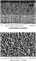
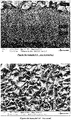
- The figures show SEM microphotographs of the samples prepared according to the examples described below.
- Figures 1a, 1b
- show SEM microphotographs of a cross section (
Figure 1a ) and of a top view onto the surface (Figure 1b ) of sample # 1 (according to the invention); - Figures 2a, 2b
- show SEM microphotographs of a cross section (
Figure 2a ) and of a top view onto the surface (Figure 2b ) of sample # 2 (according to the invention); - Figures 3a, 3b
- show SEM microphotographs of a cross section (
Figure 3a ) and of a top view onto the surface (Figure 3b ) of sample # 3 (according to the invention); - Figures 4a, 4b
- show SEM microphotographs of a cross section (
Figure 4a ) and of a top view onto the surface (Figure 4b ) of sample # 4 (comparative example); - Figures 5a, 5b
- show SEM microphotographs of a cross section (
Figure 5a ) and of a top view onto the surface (Figure 5b ) of sample # 5 (according to the invention); - Figures 6a, 6b
- show SEM microphotographs of a cross section (
Figure 6a ) and of a top view onto the surface (Figure 6b ) of sample # 6 (comparative example); - The term "fiber texture" or "texture", respectively, as used herein and as it is generally used in connection with thin films produced by vapor deposition, distinguishes the orientation of the grown grains from random orientation. Three types of textures are usually distinguished in thin films and coatings: (i) random texture, when grains have no preferred orientation; (ii) fiber texture, where the grains in the coating are oriented such that one set of geometrically equivalent crystallographic planes {h k l} is found to be preferentially oriented parallel to the substrate, while there is a rotational degree of freedom of the grains around the fiber axis which is perpendicular to this plane, and thus preferentially orientated perpendicular to the substrate; and (iii) epitaxial alignment (or in-plane texture) on single-crystal substrates, where an in-plane alignment fixes all three axes of the grain with respect to the substrate.
- The crystallographic plane of a crystal is defined by the Miller indices, h, k, l. A means to express preferred growth, i. e. that one set of geometrically equivalent crystallographic planes {h k l} is found to be preferentially oriented parallel to the substrate, is the texture coefficient TC (h k l) calculated using the Harris formula on the basis of a defined set of XRD reflections measured on the respective sample. The intensities of the XRD reflections are standardized using a JCPDF-card indicating the intensities of the XRD reflections of the same material, e. g. TiCN, but with random orientation, such as in a powder of the material. A texture coefficient TC (h k l) > 1 of a layer of crystalline material is an indication that the grains of the crystalline material are oriented with their {h k l} crystallographic plane parallel to the substrate surface more frequently than in a random distribution, at least compared to the XRD reflections used in the Harris formula to determine the texture coefficient TC.
- X-ray diffraction measurements were done on a XRD3003 PTS diffractometer of GE Sensing and Inspection Technologies using CuKα-radiation. The X-ray tube was run in point focus at 40 kV and 40 mA. A parallel beam optic using a polycapillary collimating lens with a measuring aperture of fixed size was used on the primary side whereby the irradiated area of the sample was defined in such manner that a spill over of the X-ray beam over the coated face of the sample is avoided. On the secondary side a Soller slit with a divergence of 0.4° and a 25 µm thick Ni Kβ filter were used. Symmetrical θ-2θ scans within the angle range of 20° < 2θ < 155° with increments of 0.04° and 4 seconds counting time have been conducted. On the XRD raw data intensity corrections for thin film absorption were applied to all samples which take into account the limited thickness of the layer in contrast to the natural penetration depth in a bulk material. Furthermore an absorption correction was applied for samples where an additional layer was deposited above the layer for which the TCs were calculated. Finally Kα2 stripping (Rachinger method), background subtraction and a parabolic peakfit with 5 measuring points were applied. Therefore, any XRD peak intensities indicated herein mean the accordingly corrected intensities. For the calculation of the texture coefficients TC(hkl) a formalism proposed by Harris [Harris, G. B., Philosophical Magazine Series 7, 43/336, 1952, pp. 113-123] was applied. Herein the corrected net peak intensities Icorr were correlated to the relative intensities Ipdf taken from PDF-card 00-42-1489 for TiN or TiCN layers and from PDF-card 00-046-1200 for TiAIN or TiAICN layers.

- Transmission electron microscopic (TEM) analyses were performed in a FEI Titan 80-300 microscope with field emission cathode at an acceleration voltage of 300 kV. For EDS analyses an Oxford Inca EDS system was used. The preparation of samples for TEM was made by the in-situ lift-out technique using a combined FIB/SEM equipment to cut a thin cross sectional piece out of the surface and thin the sample down to sufficient electron transparency.
- The percentage of face-centered cubic (fcc) crystal structure of the Ti1-xAlxCyNz of layer (b) was determined by EBSD analysis on polished cross-sections of the samples. The polishing was done according to the following procedure: 6 min grinding using a grinding disc Struers Piano 220 and water; 3 min polishing using Struers 9 µm MD-Largo diamond suspension; 3:40 min polishing using Struers 3µm MD-dac diamond suspension; 2 min polishing using Struers 1 µm MD-Nap diamond suspension; at least 12 min chemical polishing using Struers OP-S colloidal silica suspension with 0.04 µm average particle size. Prior to SEM / EBSD analysis the specimens were ultrasonically cleaned in ethanol and demagnetized. Inspection of the accordingly prepared specimens in the FE-SE (typically using an Everhart-Thornley secondary electron detector at 2.5 kV acceleration voltage and working distances of 3-10 mm) showed that grains of face centered cubic Ti1-xAlxCyNz layers are polished to a flat surface, showing a pronounced orientation contrast, whereas layers of h-AIN or h-AIN precipitated at grain boundaries of fcc-Ti1-xAlxCyNz layers are etched considerably stronger than fcc-phase grains, and therefore the surface of these proportions of the coating is lower than the fcc phase, and does not have a flat surface. Due to this topography, proportions in the coating which consist of h-AIN will give poor EBSD patterns in the EBSD analysis described below.
- EBSD analysis was performed in a Zeiss SUPRA40VP scanning electron microscope (SEM) with a field emission cathode using a 60 µm or 120 µm aperture and 15 kV acceleration voltage working in high current mode with a 70° incident angle of the electron beam to the polished samples surface at about 12 mm working distance. The EBSD detector was an EDAX Digiview camera, and the TSL OIM Data Collection 7 and TSL OIM Analysis 7 software packages were used for data collection and analysis, respectively. Typical acquisition and processing parameters for the EBSD maps are as follows: The map size was chosen with a length of about 25 µm parallel to the substrate surface and so that the entire thickness of the coating was covered using a ≤0.15 µm step size and a hexagonal grid of measurement points. A 4x4 or 8x8 binning and optionally a dynamic background subtraction is performed on the camera picture, using exposure times corresponding to 20 to 100 frames per second. However, as a rule, the preparation procedure described above yielded samples which gave diffraction patterns of the Ti1-xAlxCyNz layers with sufficient quality without performing background subtraction procedures. Indexing of the diffraction pattern is done by Hough transformation. The data points thus recorded should ideally be indexed with an average confidence index (CI) of > 0.2. The Cl is calculated by the TSL OIM Analysis 7 software during automated indexing of the diffraction pattern.
- In a first step, the EBSD map is cropped to get only the data points of the Ti1-xAlxCyNz layer (b) to be analysed. In a second step, grain CI standardization is carried out applying a grain tolerance angle of 5° and a minimum grain size of 5 data points. In a third step, partitioning of the so generated data set is carried out applying the filter Cl>0.1, i.e. all data points that, after grain Cl standardization, have a lower confidence index are disregarded. The ratio (number of data points indexed as fcc phase after Cl standardization and filtering / total number of data points in the cropped map) corresponds to an area ratio of fcc phase within the Ti1-xAlxCyNz layer analysed (given in area-%). However, since pattern overlap and topography at grain boundaries lead to poor indexing of EBSD patterns obtained from fcc phase Ti1-xAlxCyNz, the values thus obtained represent a minimum fraction of fcc phase in the layer, the actual fraction being higher. Typically in Ti1-xAlxCyNz coatings where XRD and SEM gives no indication of h-AIN, and which therefore consist practically of about 100% fcc phase, the EBSD measurement and processing method described above yields > 95 area-% of the EBSD map indexed as fcc phase.
- The CVD coatings were prepared in a radial flow reactor, type Bernex BPX 325S, having 1250 mm height and 325 mm outer diameter. Gas flow over the charging trays was radial from a central gas tube.
- For the preparation of cutting tools according to the present invention and of comparative examples cemented carbide cutting tool substrate bodies (composition: 90.5 wt-% WC, 1.5 wt-% TaC + NbC and 8.0 wt-% Co; geometry: SEHW1204AFN) were coated in a cylindrical CVD reactor, type Bernex BPX 325S, having a height of 1250 mm and a diameter of 325 mm.
- The gas flow over the substrate bodies was conducted radially from a central gas distribution tube, using a first and second precursor gas streams, PG1 and PG2. The first precursor gas stream, PG1, comprises, as far as required for the preparation of the desired coating, the gases AlCl3, TiCl4, CH3CN, N2 and hydrogen H2, and the second precursor gas stream, PG2, comprises, as far as required for the preparation of the desired coating, NH3 and H2. The first and second precursor gas streams, PG1 and PG2, were introduced into the reactor separately and combined immediately before entry into the reaction zone, i.e. after the outlet of the gas distribution tube.
- The experimental conditions for the deposition of the different layer types are given in the following table 1.
Table 1: Deposition conditions for CVD layers Layer type Temp. [°C] Pressure [kPa] Gas concentrations in precursor gas streams [Vol.-%] PG1 PG2 TiCl4 AlCl3 CH3CN N2 H2 NH3 H2 Ti1-xAlxN (1) 700 1 0.014 0.13 0 0 52 0.30 47.6 Ti1-xAlxN (2) 725 1 0.019 0.17 0 0 51.9 0.41 47.5 h-AIN (1) 700 0.3 0 0.24 0 0 47 1.14 51.6 h-AIN (2) 725 1 0 0.17 0 0 51.9 0.41 47.5 TiN (1) 790 2 0.44 0 0 43.3 32.5 2.16 21.6 TiN (2) 875 15 1.03 0 0 44 33 0 22 TiN (3) 850 15 1.03 0 0 44 33 0 22 TiCN (1) 825 7.5 1.77 0 0.47 10.9 65.2 0 21.7 - Coatings with different layer sequences were prepared. The following table 2 shows the layer types, layer sequences, deposition times, thicknesses, fiber textures and texture coefficients of the individual layers of samples according to the invention and of comparative samples.
- In table 2:
- L1
- = first layer immediately on substrate body surface
- L2
- = layer immediately underneath the first h-AIN layer (a)
- L(a)
- = Layer (a) of the type h-AIN
- L(b)
- = Layer (b) of the type Ti1-xAlxCyNz
- n.d.
- = not determined
- *
- = integral TC(hkl) for all Ti1-xAlxCyNz layers
- Milling operations using the cutting tool inserts of samples 1 to 6 were performed under the following conditions:
Workpiece material: Steel DIN 42CrMo4 Coolant: None Feed per tooth: fz = 0.2 mm Depth of cut: ap = 3 mm Cutting speed: vc = 283 m/min Setting angle: k = 45° - The development of the maximum flank wear, VBmax, on the main cutting edge and the number of comb cracks were observed over a milling distance of 4000 mm in 800 mm steps. The following table 3 shows the development of VBmax over the milling distance. In the milling test the cutting tool with the coating according to the present invention (sample 5) showed a significantly higher resistance against flank wear than the comparative example.
Table 3: Cutting Test Results Milling Distance [mm] Maximum Flank Wear VBmax Sample # 1 (Inv.) Sample # 2 (Inv.) Sample # 3 (Inv.) Sample # 4 (Comp.) Sample # 5 (Inv.) Sample # 6 (Comp.) 0 0 0 0 0 0 0 800 0.02 0.02 0.02 0.04 0.02 0.02 1600 0.04 0.02 0.03 0.04 0.04 0.04 2400 0.08 0.04 0.06 0.08 0.06 0.10 3200 0.12 0.08 0.08 0.10 0.10 0.18 4000 0.20 0.15 0.18 0.28 0.16 0.28
| Sample # | L1 | L2 | L(a) | L(b) | pairs of L(a)+L(b) | |
| 1 (Inv.) | Layer type | TiN (1) | Ti1-xAlxN (1) | h-AIN (1) | Ti1-xAlxN(1) | 1 |
| Deposition time [min] | 75 | 10 | 4 | 80 | ||
| Layer thickness [µm] | 3.5 | 0.7 | 0.2 | 5 | ||
| Texture (hkl)/ TC | {100} TC(100)=1.97 | {100} EBSD TC n.d. | --- | {111} TC(111)=3.27 | ||
| 2 (Inv.) | Layer type | TiN (2) | Ti1-xAlxN (2) | h-AIN (2) | Ti1-xAlxN (2) | 1 |
| Deposition time [min] | 120 | 70 | 2 | 10 | ||
| Layer thickness [µm] | 0.5 | 6 | 0.25 | 0.7 | ||
| Texture (hkl) | n.d. | {111} TC(111)=1.89* | --- | {111} TC(111)=1.89* | ||
| 3 (Inv.) | Layer type | TiN (3) | Ti1-xAlxN (2) | h-AIN (2) | Ti1-xAlxN (2) | 7 |
| Deposition time [min] | 120 | 10 | 2min/30s/5s/1s/5s/30s/1s | 7 × 10 | ||
| Layer thickness [µm] | 0.4 | 0.6 | 0.15/0.05/<0.05/<0.05/<0.05/0.05/<0.05 | 7 × 0.6 | ||
| Texture (hkl) | n.d. | {111} TC(111)=1.98* | --- | {111} TC(111)=1.98* | ||
| 4 (Comp.) | Layer type | TiN (3) | Ti1-xAlxN (2) | --- | --- | --- |
| Deposition time [min] | 120 | 90 | ||||
| Layer thickness [µm] | 0.4 | 7.5 | ||||
| Texture (hkl) | n.d. | {111} TC(111)=2.97 | ||||
| 5 (Inv.) | Layer type | TiN (2) | TiCN (1) | h-AIN (2) | Ti1-xAlxN (2) | 1 |
| Deposition time [min] | 120 | 45 | 10 | 45 | ||
| Layer thickness [µm] | 0.8 | 3 | 0.7 | 3.5 | ||
| Texture (hkl) | n.d. | {422} TC(422)=1.89 | --- | {111} TC(111)=3.05 | ||
| 6 (Comp.) | Layer type | TiN (2) | TiCN (1) | --- | Ti1-xAlxN (2) | |
| Deposition time [min] | 120 | 45 | 45 | |||
| Layer thickness [µm] | 0.8 | 3 | 3.5 | |||
| Texture (hkl) | n.d. | {211} TC(422)=3.72 | {422} EBSD TC n.d. |
Claims (13)
- A coated cutting tool consisting of a substrate of cemented carbide, cermet, ceramics, steel or cubic boron nitride and a multi-layered wear resistant coating, whereinthe multi-layered wear resistant coating has a total thickness from 5 to 25 µm and comprises refractory coating layers deposited by chemical vapour deposition (CVD) or moderate temperature chemical vapour deposition (MT-CVD), andthe multi-layered wear resistant coating comprises at least one pair of layers (a) and (b) with layer (b) being deposited immediately on top of layer (a), wherein- layer (a) is a layer of aluminium nitride having hexagonal crystal structure (h-AIN) and a thickness from 10 nm to 750 nm with a chlorine content of less than 5 at.-%, preferably less than 2.5 at.-%, most preferably less than 1 at.% or 2-3 at.-%, and- layer (b) is a layer of titanium aluminium nitride or titanium aluminium carbonitride represented by the general formula Ti1-xAlxCyNz with 0.4 ≤ x ≤ 0.95, 0 ≤ y ≤ 0.10 and 0.85 ≤ z ≤ 1.15, having a thickness from 0.5 µm to 15 µm, and at least 90% of the Ti1-xAlxCyNz of layer (b) has a face-centered cubic (fcc) crystal structure,- wherein the multi-layered wear resistant coating comprises a layer selected from the group consisting of titanium nitride (TiN), titanium carbonitride (TiCN), titanium aluminium nitride (TiAIN) and titanium aluminium carbonitride (TiAICN), said layer being deposited immediately underneath the first h-AIN layer of the type (a) and preferably having a columnar grain morphology.
- The coated cutting tool of claim 1, wherein the multi-layered wear resistant coating comprises one pair of layers (a) and (b),
or
the multi-layered wear resistant coating comprises a sequence of two or more pairs of layers (a) and (b), preferably a sequence of 2, 3, 4, 5, 6, 7, 8, 9, or 10 pairs of layers (a) and (b). - The coated cutting tool of any of the preceding claims, wherein the thickness of the h-AIN layer(s) of the type (a) is from 10 nm to 400 nm, preferably from 25 nm to 250 nm, more preferably from 40 nm to 100 nm.
- The coated cutting tool of any of the preceding claims, wherein the thickness of the fcc-Ti1-xAlxCyNz layer(s) of the type (b) is from 1 µm to 8 µm.
- The coated cutting tool of any of the preceding claims, wherein the thickness ratio of the thickness of the h-AIN layer(s) of the type (a) to the thickness of the Ti1-xAlxCyNz layer(s) of the type (b) within each pair of layers (a) and (b) with layer (b) being deposited immediately on top of layer (a) is within the range from 0.01 to 0.5.
- The coated cutting tool of any of the preceding claims, wherein the Ti1-xAlxCyNz layer(s) of the type (b) within a pair of layers (a) and (b) with layer (b) being deposited immediately on top of layer (a) has a columnar grain morphology and a preferred crystallographic growth orientation characterized by a texture coefficient TC (1 1 1) > 1.8, the TC (1 1 1) being defined as follows:
 I(111) = measured intensity of the (111) reflectionI0(111) = standard intensity of the (111) reflection of the standard powder diffraction data according to the applied JCPDF-card no. 00-046-1200I(hkl) i = measured intensity of the (hkl) i reflectionI0(hkl)i = standard intensity of the (hkl) i reflection of the standard powder diffraction data according to the applied JCPDF-card no. 00-046-1200n = number of reflections used in the calculation (here: n = 4)(hkl)i the (hkl)i reflections used are: (111), (200), (220) and (311).
 - The coated cutting tool of any of the preceding claims, wherein the layer deposited immediately underneath the first h-AIN layer of the type (a) has a preferred crystallographic growth orientation characterized by a texture coefficient TC (2 0 0) > 1.8, the TC (2 0 0) being defined as follows:
 I(200) = measured intensity of the (200) reflectionI0(200) = standard intensity of the (200) reflection of the standard powder diffraction data according to the applied JCPDF-card no. 00-046-1200 when the said layer is a TiAIN or TiAICN layer, and according to JCPDF card no. 00-42-1489 when the said layer is a TiN or TiCN layerI(hkl) i = measured intensity of the (hkl)i reflectionI0(hkl)i = standard intensity of the (hkl) i reflection of the standard powder diffraction data according to the applied JCPDF-card no. 00-046-1200 when the said layer is a TiAIN or TiAICN layer, and according to JCPDF card no. 00-42-1489 when the said layer is a TiN or TiCN layern = number of reflections used in the calculation (here: n = 4)(hkl)i the (hkl)i reflections used are: (111), (200), (220) and (311).
 - The coated cutting tool of any of the preceding claims, wherein the layer deposited immediately underneath the first h-AIN layer of the type (a) is a layer of titanium carbonitride (TiCN) and has a preferred crystallographic growth orientation characterized by a texture coefficient TC (4 2 2) > 1.8, the TC (4 2 2) being defined as follows:
 I(422) = measured intensity of the (422) reflectionI0(422) = standard intensity of the (422) reflection of the standard powder diffraction data according to the applied JCPDF-card no. 00-42-1489I(hkl) i = measured intensity of the (hkl) i reflectionI0(hkl)i = standard intensity of the (hkl) i reflection of the standard powder diffraction data according to the applied JCPDF-card no. 00-42-1489n = number of reflections used in the calculation (here: n = 5)(hkl)i the (hkl)i reflections used are: (111), (200), (220), (311) and (422).
 - The coated cutting tool of any of the preceding claims, wherein the layer deposited immediately underneath the first h-AIN layer of the type (a) is a layer of titanium aluminium nitride (TiAIN) or titanium aluminium carbonitride (TiAICN) and has a preferred crystallographic growth orientation characterized by a texture coefficient TC (1 1 1) > 1.8, the TC (1 1 1) being defined as follows:
 I(111) = measured intensity of the (111) reflectionI0(111) = standard intensity of the (111) reflection of the standard powder diffraction data according to the applied JCPDF-card no. 00-046-1200I(hkl) i = measured intensity of the (hkl) i reflectionI0(hkl)i = standard intensity of the (hkl)i reflection of the standard powder diffraction data according to the applied JCPDF-card no. 00-046-1200n = number of reflections used in the calculation (here: n = 4)(hkl)i the (hkl)i reflections used are: (111), (200), (220) and (311).
 - The coated cutting tool of any of the preceding claims, wherein at least 95%, preferably at least 97% of the Ti1-xAlxCyNz of layer (b) have face-centered cubic (fcc) crystal structure.
- The coated cutting tool of any of the preceding claims, wherein the W content of said first h-AIN layer(s) of the type (a) is less than 0.1 at.-%.
- The coated cutting tool of any of the preceding claims, wherein the Co content of said first h-AIN layer(s) of the type (a) is less than 0.1 at.-%.
- The coated cutting tool of any of the preceding claims, wherein the Ti content of said first h-AIN layer(s) of the type (a) is less than 0.5 at.-%, preferably less than 0.3 at.-%.
Applications Claiming Priority (2)
| Application Number | Priority Date | Filing Date | Title |
|---|---|---|---|
| EP16163243 | 2016-03-31 | ||
| PCT/EP2017/057728 WO2017167980A1 (en) | 2016-03-31 | 2017-03-31 | Coated cutting tool with h-aln and ti1-xalxcynz layers |
Publications (2)
| Publication Number | Publication Date |
|---|---|
| EP3436619A1 EP3436619A1 (en) | 2019-02-06 |
| EP3436619B1 true EP3436619B1 (en) | 2022-04-20 |
Family
ID=55646440
Family Applications (1)
| Application Number | Title | Priority Date | Filing Date |
|---|---|---|---|
| EP17713979.7A Active EP3436619B1 (en) | 2016-03-31 | 2017-03-31 | Coated cutting tool with h-aln and ti1-xalxcynz layers |
Country Status (6)
| Country | Link |
|---|---|
| US (1) | US11247276B2 (en) |
| EP (1) | EP3436619B1 (en) |
| JP (1) | JP2019511378A (en) |
| KR (1) | KR102372121B1 (en) |
| CN (1) | CN108884562A (en) |
| WO (1) | WO2017167980A1 (en) |
Families Citing this family (16)
| Publication number | Priority date | Publication date | Assignee | Title |
|---|---|---|---|---|
| EP3228726A1 (en) * | 2016-04-08 | 2017-10-11 | Seco Tools Ab | Coated cutting tool |
| JP7393946B2 (en) * | 2017-04-07 | 2023-12-07 | サンドビック インテレクチュアル プロパティー アクティエボラーグ | coated cutting tools |
| JP6565093B1 (en) * | 2018-03-22 | 2019-08-28 | 住友電工ハードメタル株式会社 | Surface-coated cutting tool and manufacturing method thereof |
| US11326252B2 (en) | 2018-03-22 | 2022-05-10 | Sumitomo Electric Hardmetal Corp. | Surface-coated cutting tool and method for manufacturing same |
| JP6565092B1 (en) | 2018-03-22 | 2019-08-28 | 住友電工ハードメタル株式会社 | Surface-coated cutting tool and manufacturing method thereof |
| WO2020138304A1 (en) * | 2018-12-27 | 2020-07-02 | 三菱マテリアル株式会社 | Surface-coated cutting tool |
| BR112021023538A2 (en) * | 2019-05-27 | 2022-01-18 | Sandvik Coromant Ab | A coated cutting tool |
| CN110158046B (en) * | 2019-07-02 | 2021-08-20 | 富耐克超硬材料股份有限公司 | Composite coating, self-lubricating composite coating cutter and preparation method thereof |
| EP3872222B1 (en) * | 2020-02-28 | 2022-12-28 | AB Sandvik Coromant | A coated cutting tool |
| CN115297980A (en) | 2020-03-25 | 2022-11-04 | 三菱综合材料株式会社 | Surface-coated cutting tool |
| CN111438380B (en) * | 2020-05-22 | 2021-07-30 | 株洲钻石切削刀具股份有限公司 | Surface coating cutting tool and method for manufacturing same |
| CN113740366B (en) * | 2020-05-27 | 2023-11-28 | 中国兵器工业第五九研究所 | Method and device for nondestructively detecting crystal orientation difference and grain boundary defect in monocrystal or directional crystal |
| CN114737165B (en) * | 2022-03-18 | 2023-05-12 | 赣州澳克泰工具技术有限公司 | Coated cutting tool and preparation method thereof |
| CN114686883B (en) * | 2022-04-07 | 2023-04-28 | 赣州澳克泰工具技术有限公司 | Cutting tool with gradient multilayer coating and preparation method thereof |
| CN115351279B (en) * | 2022-08-30 | 2023-11-21 | 株洲钻石切削刀具股份有限公司 | Coated cemented carbide cutting tool |
| CN115351317A (en) * | 2022-08-30 | 2022-11-18 | 株洲钻石切削刀具股份有限公司 | Coated cutting tool and method of making same |
Family Cites Families (18)
| Publication number | Priority date | Publication date | Assignee | Title |
|---|---|---|---|---|
| DE69319531T2 (en) | 1992-10-12 | 1999-04-15 | Sumitomo Electric Industries, Ltd., Osaka | Ultra thin film laminate |
| JP2002273607A (en) | 2001-03-16 | 2002-09-25 | Hitachi Tool Engineering Ltd | Multilayer coat tool |
| US7785700B2 (en) * | 2004-04-13 | 2010-08-31 | Sumitomo Electric Hardmetal Corp. | Surface-coated cutting tool |
| US7597970B2 (en) * | 2005-03-22 | 2009-10-06 | Kyocera Corporation | Surface coated member and cutting tool |
| JP4832108B2 (en) * | 2005-03-29 | 2011-12-07 | 京セラ株式会社 | Surface coated cutting tool |
| SE531971C2 (en) | 2007-08-24 | 2009-09-15 | Seco Tools Ab | Coated cutting tool for general turning in hot-strength super alloys (HRSA) |
| EP2247772B1 (en) * | 2008-02-21 | 2016-06-29 | Seco Tools AB | Multilayered coated cutting tool |
| DE102008013966A1 (en) * | 2008-03-12 | 2009-09-17 | Kennametal Inc. | Hard material coated body |
| US9394031B2 (en) | 2009-07-16 | 2016-07-19 | Shimano Inc. | Bar end electric shifter for bicycle |
| EP2604720A1 (en) | 2011-12-14 | 2013-06-19 | Sandvik Intellectual Property Ab | Coated cutting tool and method of manufacturing the same |
| JP5417649B2 (en) | 2012-05-08 | 2014-02-19 | 住友電工ハードメタル株式会社 | Surface coated cutting tool |
| JP6090063B2 (en) | 2012-08-28 | 2017-03-08 | 三菱マテリアル株式会社 | Surface coated cutting tool |
| JP6044336B2 (en) | 2012-12-27 | 2016-12-14 | 三菱マテリアル株式会社 | Surface coated cutting tool with excellent chipping resistance due to hard coating layer |
| JP2014184522A (en) | 2013-03-25 | 2014-10-02 | Mitsubishi Materials Corp | Surface-coated wc-based super hard alloy-made cutting tool with hard coating layer exhibiting superior adhesiveness |
| DE102013104254A1 (en) * | 2013-04-26 | 2014-10-30 | Walter Ag | Tool with CVD coating |
| JP6238131B2 (en) * | 2013-12-26 | 2017-11-29 | 住友電工ハードメタル株式会社 | Coating and cutting tools |
| JP6296294B2 (en) | 2014-07-30 | 2018-03-20 | 三菱マテリアル株式会社 | Surface coated cutting tool with excellent chipping resistance due to hard coating layer |
| EP3000913B1 (en) * | 2014-09-26 | 2020-07-29 | Walter Ag | Coated cutting tool insert with MT-CVD TiCN on TiAI(C,N) |
-
2017
- 2017-03-31 KR KR1020187029760A patent/KR102372121B1/en active IP Right Grant
- 2017-03-31 EP EP17713979.7A patent/EP3436619B1/en active Active
- 2017-03-31 JP JP2018551097A patent/JP2019511378A/en active Pending
- 2017-03-31 US US16/090,287 patent/US11247276B2/en active Active
- 2017-03-31 CN CN201780018229.XA patent/CN108884562A/en active Pending
- 2017-03-31 WO PCT/EP2017/057728 patent/WO2017167980A1/en active Application Filing
Also Published As
| Publication number | Publication date |
|---|---|
| US11247276B2 (en) | 2022-02-15 |
| KR102372121B1 (en) | 2022-03-07 |
| CN108884562A (en) | 2018-11-23 |
| EP3436619A1 (en) | 2019-02-06 |
| WO2017167980A1 (en) | 2017-10-05 |
| KR20180130520A (en) | 2018-12-07 |
| JP2019511378A (en) | 2019-04-25 |
| US20190111497A1 (en) | 2019-04-18 |
Similar Documents
| Publication | Publication Date | Title |
|---|---|---|
| EP3436619B1 (en) | Coated cutting tool with h-aln and ti1-xalxcynz layers | |
| US10407777B2 (en) | Coated cutting tool insert with MT-CVD TiCN on TiAI(C,N) | |
| RU2675190C2 (en) | Alumina-coated cutting tool | |
| EP3263738B1 (en) | Cutting tool with textured alumina layer | |
| US9956667B2 (en) | Coated cutting tool | |
| EP2902528B1 (en) | Alumina coated cutting tool with zigzag alumina grain boundaries | |
| US9863064B2 (en) | Surface-coated cutting tool | |
| KR20180128531A (en) | Surface-coated cutting tool and method of producing the same | |
| KR20180135497A (en) | Surface-coated cutting tool and method of producing the same | |
| KR20120073322A (en) | Coated tool | |
| WO2018138255A1 (en) | Coated cutting tool | |
| WO2017175400A1 (en) | Surface-coated cutting tool and method for producing same | |
| JP6047268B1 (en) | Surface coated cutting tool |
Legal Events
| Date | Code | Title | Description |
|---|---|---|---|
| STAA | Information on the status of an ep patent application or granted ep patent |
Free format text: STATUS: UNKNOWN |
|
| STAA | Information on the status of an ep patent application or granted ep patent |
Free format text: STATUS: THE INTERNATIONAL PUBLICATION HAS BEEN MADE |
|
| PUAI | Public reference made under article 153(3) epc to a published international application that has entered the european phase |
Free format text: ORIGINAL CODE: 0009012 |
|
| STAA | Information on the status of an ep patent application or granted ep patent |
Free format text: STATUS: REQUEST FOR EXAMINATION WAS MADE |
|
| 17P | Request for examination filed |
Effective date: 20181031 |
|
| AK | Designated contracting states |
Kind code of ref document: A1 Designated state(s): AL AT BE BG CH CY CZ DE DK EE ES FI FR GB GR HR HU IE IS IT LI LT LU LV MC MK MT NL NO PL PT RO RS SE SI SK SM TR |
|
| AX | Request for extension of the european patent |
Extension state: BA ME |
|
| STAA | Information on the status of an ep patent application or granted ep patent |
Free format text: STATUS: REQUEST FOR EXAMINATION WAS MADE |
|
| DAV | Request for validation of the european patent (deleted) | ||
| DAX | Request for extension of the european patent (deleted) | ||
| GRAP | Despatch of communication of intention to grant a patent |
Free format text: ORIGINAL CODE: EPIDOSNIGR1 |
|
| STAA | Information on the status of an ep patent application or granted ep patent |
Free format text: STATUS: GRANT OF PATENT IS INTENDED |
|
| INTG | Intention to grant announced |
Effective date: 20211203 |
|
| GRAS | Grant fee paid |
Free format text: ORIGINAL CODE: EPIDOSNIGR3 |
|
| GRAA | (expected) grant |
Free format text: ORIGINAL CODE: 0009210 |
|
| STAA | Information on the status of an ep patent application or granted ep patent |
Free format text: STATUS: THE PATENT HAS BEEN GRANTED |
|
| AK | Designated contracting states |
Kind code of ref document: B1 Designated state(s): AL AT BE BG CH CY CZ DE DK EE ES FI FR GB GR HR HU IE IS IT LI LT LU LV MC MK MT NL NO PL PT RO RS SE SI SK SM TR |
|
| REG | Reference to a national code |
Ref country code: GB Ref legal event code: FG4D |
|
| REG | Reference to a national code |
Ref country code: CH Ref legal event code: EP |
|
| REG | Reference to a national code |
Ref country code: IE Ref legal event code: FG4D |
|
| REG | Reference to a national code |
Ref country code: DE Ref legal event code: R096 Ref document number: 602017056215 Country of ref document: DE |
|
| REG | Reference to a national code |
Ref country code: AT Ref legal event code: REF Ref document number: 1485203 Country of ref document: AT Kind code of ref document: T Effective date: 20220515 |
|
| REG | Reference to a national code |
Ref country code: LT Ref legal event code: MG9D |
|
| REG | Reference to a national code |
Ref country code: NL Ref legal event code: MP Effective date: 20220420 |
|
| REG | Reference to a national code |
Ref country code: AT Ref legal event code: MK05 Ref document number: 1485203 Country of ref document: AT Kind code of ref document: T Effective date: 20220420 |
|
| PG25 | Lapsed in a contracting state [announced via postgrant information from national office to epo] |
Ref country code: NL Free format text: LAPSE BECAUSE OF FAILURE TO SUBMIT A TRANSLATION OF THE DESCRIPTION OR TO PAY THE FEE WITHIN THE PRESCRIBED TIME-LIMIT Effective date: 20220420 |
|
| PG25 | Lapsed in a contracting state [announced via postgrant information from national office to epo] |
Ref country code: SE Free format text: LAPSE BECAUSE OF FAILURE TO SUBMIT A TRANSLATION OF THE DESCRIPTION OR TO PAY THE FEE WITHIN THE PRESCRIBED TIME-LIMIT Effective date: 20220420 Ref country code: PT Free format text: LAPSE BECAUSE OF FAILURE TO SUBMIT A TRANSLATION OF THE DESCRIPTION OR TO PAY THE FEE WITHIN THE PRESCRIBED TIME-LIMIT Effective date: 20220822 Ref country code: NO Free format text: LAPSE BECAUSE OF FAILURE TO SUBMIT A TRANSLATION OF THE DESCRIPTION OR TO PAY THE FEE WITHIN THE PRESCRIBED TIME-LIMIT Effective date: 20220720 Ref country code: LT Free format text: LAPSE BECAUSE OF FAILURE TO SUBMIT A TRANSLATION OF THE DESCRIPTION OR TO PAY THE FEE WITHIN THE PRESCRIBED TIME-LIMIT Effective date: 20220420 Ref country code: HR Free format text: LAPSE BECAUSE OF FAILURE TO SUBMIT A TRANSLATION OF THE DESCRIPTION OR TO PAY THE FEE WITHIN THE PRESCRIBED TIME-LIMIT Effective date: 20220420 Ref country code: GR Free format text: LAPSE BECAUSE OF FAILURE TO SUBMIT A TRANSLATION OF THE DESCRIPTION OR TO PAY THE FEE WITHIN THE PRESCRIBED TIME-LIMIT Effective date: 20220721 Ref country code: FI Free format text: LAPSE BECAUSE OF FAILURE TO SUBMIT A TRANSLATION OF THE DESCRIPTION OR TO PAY THE FEE WITHIN THE PRESCRIBED TIME-LIMIT Effective date: 20220420 Ref country code: ES Free format text: LAPSE BECAUSE OF FAILURE TO SUBMIT A TRANSLATION OF THE DESCRIPTION OR TO PAY THE FEE WITHIN THE PRESCRIBED TIME-LIMIT Effective date: 20220420 Ref country code: BG Free format text: LAPSE BECAUSE OF FAILURE TO SUBMIT A TRANSLATION OF THE DESCRIPTION OR TO PAY THE FEE WITHIN THE PRESCRIBED TIME-LIMIT Effective date: 20220720 Ref country code: AT Free format text: LAPSE BECAUSE OF FAILURE TO SUBMIT A TRANSLATION OF THE DESCRIPTION OR TO PAY THE FEE WITHIN THE PRESCRIBED TIME-LIMIT Effective date: 20220420 |
|
| PG25 | Lapsed in a contracting state [announced via postgrant information from national office to epo] |
Ref country code: RS Free format text: LAPSE BECAUSE OF FAILURE TO SUBMIT A TRANSLATION OF THE DESCRIPTION OR TO PAY THE FEE WITHIN THE PRESCRIBED TIME-LIMIT Effective date: 20220420 Ref country code: PL Free format text: LAPSE BECAUSE OF FAILURE TO SUBMIT A TRANSLATION OF THE DESCRIPTION OR TO PAY THE FEE WITHIN THE PRESCRIBED TIME-LIMIT Effective date: 20220420 Ref country code: LV Free format text: LAPSE BECAUSE OF FAILURE TO SUBMIT A TRANSLATION OF THE DESCRIPTION OR TO PAY THE FEE WITHIN THE PRESCRIBED TIME-LIMIT Effective date: 20220420 Ref country code: IS Free format text: LAPSE BECAUSE OF FAILURE TO SUBMIT A TRANSLATION OF THE DESCRIPTION OR TO PAY THE FEE WITHIN THE PRESCRIBED TIME-LIMIT Effective date: 20220820 |
|
| REG | Reference to a national code |
Ref country code: DE Ref legal event code: R097 Ref document number: 602017056215 Country of ref document: DE |
|
| PG25 | Lapsed in a contracting state [announced via postgrant information from national office to epo] |
Ref country code: SM Free format text: LAPSE BECAUSE OF FAILURE TO SUBMIT A TRANSLATION OF THE DESCRIPTION OR TO PAY THE FEE WITHIN THE PRESCRIBED TIME-LIMIT Effective date: 20220420 Ref country code: SK Free format text: LAPSE BECAUSE OF FAILURE TO SUBMIT A TRANSLATION OF THE DESCRIPTION OR TO PAY THE FEE WITHIN THE PRESCRIBED TIME-LIMIT Effective date: 20220420 Ref country code: RO Free format text: LAPSE BECAUSE OF FAILURE TO SUBMIT A TRANSLATION OF THE DESCRIPTION OR TO PAY THE FEE WITHIN THE PRESCRIBED TIME-LIMIT Effective date: 20220420 Ref country code: EE Free format text: LAPSE BECAUSE OF FAILURE TO SUBMIT A TRANSLATION OF THE DESCRIPTION OR TO PAY THE FEE WITHIN THE PRESCRIBED TIME-LIMIT Effective date: 20220420 Ref country code: DK Free format text: LAPSE BECAUSE OF FAILURE TO SUBMIT A TRANSLATION OF THE DESCRIPTION OR TO PAY THE FEE WITHIN THE PRESCRIBED TIME-LIMIT Effective date: 20220420 Ref country code: CZ Free format text: LAPSE BECAUSE OF FAILURE TO SUBMIT A TRANSLATION OF THE DESCRIPTION OR TO PAY THE FEE WITHIN THE PRESCRIBED TIME-LIMIT Effective date: 20220420 |
|
| PLBE | No opposition filed within time limit |
Free format text: ORIGINAL CODE: 0009261 |
|
| STAA | Information on the status of an ep patent application or granted ep patent |
Free format text: STATUS: NO OPPOSITION FILED WITHIN TIME LIMIT |
|
| 26N | No opposition filed |
Effective date: 20230123 |
|
| PG25 | Lapsed in a contracting state [announced via postgrant information from national office to epo] |
Ref country code: AL Free format text: LAPSE BECAUSE OF FAILURE TO SUBMIT A TRANSLATION OF THE DESCRIPTION OR TO PAY THE FEE WITHIN THE PRESCRIBED TIME-LIMIT Effective date: 20220420 |
|
| PG25 | Lapsed in a contracting state [announced via postgrant information from national office to epo] |
Ref country code: SI Free format text: LAPSE BECAUSE OF FAILURE TO SUBMIT A TRANSLATION OF THE DESCRIPTION OR TO PAY THE FEE WITHIN THE PRESCRIBED TIME-LIMIT Effective date: 20220420 |
|
| P01 | Opt-out of the competence of the unified patent court (upc) registered |
Effective date: 20230603 |
|
| PG25 | Lapsed in a contracting state [announced via postgrant information from national office to epo] |
Ref country code: MC Free format text: LAPSE BECAUSE OF FAILURE TO SUBMIT A TRANSLATION OF THE DESCRIPTION OR TO PAY THE FEE WITHIN THE PRESCRIBED TIME-LIMIT Effective date: 20220420 |
|
| REG | Reference to a national code |
Ref country code: CH Ref legal event code: PL |
|
| REG | Reference to a national code |
Ref country code: BE Ref legal event code: MM Effective date: 20230331 |
|
| PG25 | Lapsed in a contracting state [announced via postgrant information from national office to epo] |
Ref country code: LU Free format text: LAPSE BECAUSE OF NON-PAYMENT OF DUE FEES Effective date: 20230331 |
|
| REG | Reference to a national code |
Ref country code: IE Ref legal event code: MM4A |
|
| PG25 | Lapsed in a contracting state [announced via postgrant information from national office to epo] |
Ref country code: LI Free format text: LAPSE BECAUSE OF NON-PAYMENT OF DUE FEES Effective date: 20230331 Ref country code: IE Free format text: LAPSE BECAUSE OF NON-PAYMENT OF DUE FEES Effective date: 20230331 Ref country code: CH Free format text: LAPSE BECAUSE OF NON-PAYMENT OF DUE FEES Effective date: 20230331 |
|
| PG25 | Lapsed in a contracting state [announced via postgrant information from national office to epo] |
Ref country code: BE Free format text: LAPSE BECAUSE OF NON-PAYMENT OF DUE FEES Effective date: 20230331 |
|
| PGFP | Annual fee paid to national office [announced via postgrant information from national office to epo] |
Ref country code: DE Payment date: 20240206 Year of fee payment: 8 Ref country code: GB Payment date: 20240208 Year of fee payment: 8 |
|
| PGFP | Annual fee paid to national office [announced via postgrant information from national office to epo] |
Ref country code: IT Payment date: 20240212 Year of fee payment: 8 Ref country code: FR Payment date: 20240223 Year of fee payment: 8 |