WO2017010495A1 - 圧電センサ、タッチパネル、タッチ式入力装置および表示装置 - Google Patents
圧電センサ、タッチパネル、タッチ式入力装置および表示装置 Download PDFInfo
- Publication number
- WO2017010495A1 WO2017010495A1 PCT/JP2016/070631 JP2016070631W WO2017010495A1 WO 2017010495 A1 WO2017010495 A1 WO 2017010495A1 JP 2016070631 W JP2016070631 W JP 2016070631W WO 2017010495 A1 WO2017010495 A1 WO 2017010495A1
- Authority
- WO
- WIPO (PCT)
- Prior art keywords
- piezoelectric sheet
- piezoelectric
- optical compensation
- electrode
- piezoelectric sensor
- Prior art date
- Legal status (The legal status is an assumption and is not a legal conclusion. Google has not performed a legal analysis and makes no representation as to the accuracy of the status listed.)
- Ceased
Links
Images



Classifications
-
- G—PHYSICS
- G02—OPTICS
- G02B—OPTICAL ELEMENTS, SYSTEMS OR APPARATUS
- G02B5/00—Optical elements other than lenses
- G02B5/30—Polarising elements
- G02B5/3083—Birefringent or phase retarding elements
-
- G—PHYSICS
- G02—OPTICS
- G02F—OPTICAL DEVICES OR ARRANGEMENTS FOR THE CONTROL OF LIGHT BY MODIFICATION OF THE OPTICAL PROPERTIES OF THE MEDIA OF THE ELEMENTS INVOLVED THEREIN; NON-LINEAR OPTICS; FREQUENCY-CHANGING OF LIGHT; OPTICAL LOGIC ELEMENTS; OPTICAL ANALOGUE/DIGITAL CONVERTERS
- G02F1/00—Devices or arrangements for the control of the intensity, colour, phase, polarisation or direction of light arriving from an independent light source, e.g. switching, gating or modulating; Non-linear optics
- G02F1/01—Devices or arrangements for the control of the intensity, colour, phase, polarisation or direction of light arriving from an independent light source, e.g. switching, gating or modulating; Non-linear optics for the control of the intensity, phase, polarisation or colour
- G02F1/13—Devices or arrangements for the control of the intensity, colour, phase, polarisation or direction of light arriving from an independent light source, e.g. switching, gating or modulating; Non-linear optics for the control of the intensity, phase, polarisation or colour based on liquid crystals, e.g. single liquid crystal display cells
- G02F1/133—Constructional arrangements; Operation of liquid crystal cells; Circuit arrangements
- G02F1/13306—Circuit arrangements or driving methods for the control of single liquid crystal cells
-
- G—PHYSICS
- G02—OPTICS
- G02F—OPTICAL DEVICES OR ARRANGEMENTS FOR THE CONTROL OF LIGHT BY MODIFICATION OF THE OPTICAL PROPERTIES OF THE MEDIA OF THE ELEMENTS INVOLVED THEREIN; NON-LINEAR OPTICS; FREQUENCY-CHANGING OF LIGHT; OPTICAL LOGIC ELEMENTS; OPTICAL ANALOGUE/DIGITAL CONVERTERS
- G02F1/00—Devices or arrangements for the control of the intensity, colour, phase, polarisation or direction of light arriving from an independent light source, e.g. switching, gating or modulating; Non-linear optics
- G02F1/01—Devices or arrangements for the control of the intensity, colour, phase, polarisation or direction of light arriving from an independent light source, e.g. switching, gating or modulating; Non-linear optics for the control of the intensity, phase, polarisation or colour
- G02F1/13—Devices or arrangements for the control of the intensity, colour, phase, polarisation or direction of light arriving from an independent light source, e.g. switching, gating or modulating; Non-linear optics for the control of the intensity, phase, polarisation or colour based on liquid crystals, e.g. single liquid crystal display cells
- G02F1/133—Constructional arrangements; Operation of liquid crystal cells; Circuit arrangements
- G02F1/1333—Constructional arrangements; Manufacturing methods
- G02F1/13338—Input devices, e.g. touch panels
-
- G—PHYSICS
- G02—OPTICS
- G02F—OPTICAL DEVICES OR ARRANGEMENTS FOR THE CONTROL OF LIGHT BY MODIFICATION OF THE OPTICAL PROPERTIES OF THE MEDIA OF THE ELEMENTS INVOLVED THEREIN; NON-LINEAR OPTICS; FREQUENCY-CHANGING OF LIGHT; OPTICAL LOGIC ELEMENTS; OPTICAL ANALOGUE/DIGITAL CONVERTERS
- G02F1/00—Devices or arrangements for the control of the intensity, colour, phase, polarisation or direction of light arriving from an independent light source, e.g. switching, gating or modulating; Non-linear optics
- G02F1/01—Devices or arrangements for the control of the intensity, colour, phase, polarisation or direction of light arriving from an independent light source, e.g. switching, gating or modulating; Non-linear optics for the control of the intensity, phase, polarisation or colour
- G02F1/13—Devices or arrangements for the control of the intensity, colour, phase, polarisation or direction of light arriving from an independent light source, e.g. switching, gating or modulating; Non-linear optics for the control of the intensity, phase, polarisation or colour based on liquid crystals, e.g. single liquid crystal display cells
- G02F1/133—Constructional arrangements; Operation of liquid crystal cells; Circuit arrangements
- G02F1/1333—Constructional arrangements; Manufacturing methods
- G02F1/1335—Structural association of cells with optical devices, e.g. polarisers or reflectors
- G02F1/133528—Polarisers
-
- G—PHYSICS
- G02—OPTICS
- G02F—OPTICAL DEVICES OR ARRANGEMENTS FOR THE CONTROL OF LIGHT BY MODIFICATION OF THE OPTICAL PROPERTIES OF THE MEDIA OF THE ELEMENTS INVOLVED THEREIN; NON-LINEAR OPTICS; FREQUENCY-CHANGING OF LIGHT; OPTICAL LOGIC ELEMENTS; OPTICAL ANALOGUE/DIGITAL CONVERTERS
- G02F1/00—Devices or arrangements for the control of the intensity, colour, phase, polarisation or direction of light arriving from an independent light source, e.g. switching, gating or modulating; Non-linear optics
- G02F1/01—Devices or arrangements for the control of the intensity, colour, phase, polarisation or direction of light arriving from an independent light source, e.g. switching, gating or modulating; Non-linear optics for the control of the intensity, phase, polarisation or colour
- G02F1/13—Devices or arrangements for the control of the intensity, colour, phase, polarisation or direction of light arriving from an independent light source, e.g. switching, gating or modulating; Non-linear optics for the control of the intensity, phase, polarisation or colour based on liquid crystals, e.g. single liquid crystal display cells
- G02F1/133—Constructional arrangements; Operation of liquid crystal cells; Circuit arrangements
- G02F1/1333—Constructional arrangements; Manufacturing methods
- G02F1/1335—Structural association of cells with optical devices, e.g. polarisers or reflectors
- G02F1/13363—Birefringent elements, e.g. for optical compensation
-
- G—PHYSICS
- G06—COMPUTING OR CALCULATING; COUNTING
- G06F—ELECTRIC DIGITAL DATA PROCESSING
- G06F3/00—Input arrangements for transferring data to be processed into a form capable of being handled by the computer; Output arrangements for transferring data from processing unit to output unit, e.g. interface arrangements
- G06F3/01—Input arrangements or combined input and output arrangements for interaction between user and computer
- G06F3/03—Arrangements for converting the position or the displacement of a member into a coded form
- G06F3/041—Digitisers, e.g. for touch screens or touch pads, characterised by the transducing means
- G06F3/0412—Digitisers structurally integrated in a display
-
- G—PHYSICS
- G06—COMPUTING OR CALCULATING; COUNTING
- G06F—ELECTRIC DIGITAL DATA PROCESSING
- G06F3/00—Input arrangements for transferring data to be processed into a form capable of being handled by the computer; Output arrangements for transferring data from processing unit to output unit, e.g. interface arrangements
- G06F3/01—Input arrangements or combined input and output arrangements for interaction between user and computer
- G06F3/03—Arrangements for converting the position or the displacement of a member into a coded form
- G06F3/041—Digitisers, e.g. for touch screens or touch pads, characterised by the transducing means
- G06F3/044—Digitisers, e.g. for touch screens or touch pads, characterised by the transducing means by capacitive means
- G06F3/0445—Digitisers, e.g. for touch screens or touch pads, characterised by the transducing means by capacitive means using two or more layers of sensing electrodes, e.g. using two layers of electrodes separated by a dielectric layer
-
- H—ELECTRICITY
- H10—SEMICONDUCTOR DEVICES; ELECTRIC SOLID-STATE DEVICES NOT OTHERWISE PROVIDED FOR
- H10N—ELECTRIC SOLID-STATE DEVICES NOT OTHERWISE PROVIDED FOR
- H10N30/00—Piezoelectric or electrostrictive devices
- H10N30/30—Piezoelectric or electrostrictive devices with mechanical input and electrical output, e.g. functioning as generators or sensors
- H10N30/302—Sensors
-
- H—ELECTRICITY
- H10—SEMICONDUCTOR DEVICES; ELECTRIC SOLID-STATE DEVICES NOT OTHERWISE PROVIDED FOR
- H10N—ELECTRIC SOLID-STATE DEVICES NOT OTHERWISE PROVIDED FOR
- H10N30/00—Piezoelectric or electrostrictive devices
- H10N30/704—Piezoelectric or electrostrictive devices based on piezoelectric or electrostrictive films or coatings
-
- H—ELECTRICITY
- H10—SEMICONDUCTOR DEVICES; ELECTRIC SOLID-STATE DEVICES NOT OTHERWISE PROVIDED FOR
- H10N—ELECTRIC SOLID-STATE DEVICES NOT OTHERWISE PROVIDED FOR
- H10N30/00—Piezoelectric or electrostrictive devices
- H10N30/80—Constructional details
- H10N30/85—Piezoelectric or electrostrictive active materials
- H10N30/857—Macromolecular compositions
-
- H—ELECTRICITY
- H10—SEMICONDUCTOR DEVICES; ELECTRIC SOLID-STATE DEVICES NOT OTHERWISE PROVIDED FOR
- H10N—ELECTRIC SOLID-STATE DEVICES NOT OTHERWISE PROVIDED FOR
- H10N30/00—Piezoelectric or electrostrictive devices
- H10N30/80—Constructional details
- H10N30/87—Electrodes or interconnections, e.g. leads or terminals
- H10N30/877—Conductive materials
-
- H—ELECTRICITY
- H10—SEMICONDUCTOR DEVICES; ELECTRIC SOLID-STATE DEVICES NOT OTHERWISE PROVIDED FOR
- H10N—ELECTRIC SOLID-STATE DEVICES NOT OTHERWISE PROVIDED FOR
- H10N30/00—Piezoelectric or electrostrictive devices
- H10N30/80—Constructional details
- H10N30/87—Electrodes or interconnections, e.g. leads or terminals
- H10N30/877—Conductive materials
- H10N30/878—Conductive materials the principal material being non-metallic, e.g. oxide or carbon based
-
- G—PHYSICS
- G02—OPTICS
- G02F—OPTICAL DEVICES OR ARRANGEMENTS FOR THE CONTROL OF LIGHT BY MODIFICATION OF THE OPTICAL PROPERTIES OF THE MEDIA OF THE ELEMENTS INVOLVED THEREIN; NON-LINEAR OPTICS; FREQUENCY-CHANGING OF LIGHT; OPTICAL LOGIC ELEMENTS; OPTICAL ANALOGUE/DIGITAL CONVERTERS
- G02F1/00—Devices or arrangements for the control of the intensity, colour, phase, polarisation or direction of light arriving from an independent light source, e.g. switching, gating or modulating; Non-linear optics
- G02F1/01—Devices or arrangements for the control of the intensity, colour, phase, polarisation or direction of light arriving from an independent light source, e.g. switching, gating or modulating; Non-linear optics for the control of the intensity, phase, polarisation or colour
- G02F1/13—Devices or arrangements for the control of the intensity, colour, phase, polarisation or direction of light arriving from an independent light source, e.g. switching, gating or modulating; Non-linear optics for the control of the intensity, phase, polarisation or colour based on liquid crystals, e.g. single liquid crystal display cells
- G02F1/133—Constructional arrangements; Operation of liquid crystal cells; Circuit arrangements
- G02F1/1333—Constructional arrangements; Manufacturing methods
- G02F1/133394—Piezoelectric elements associated with the cells
-
- G—PHYSICS
- G06—COMPUTING OR CALCULATING; COUNTING
- G06F—ELECTRIC DIGITAL DATA PROCESSING
- G06F2203/00—Indexing scheme relating to G06F3/00 - G06F3/048
- G06F2203/041—Indexing scheme relating to G06F3/041 - G06F3/045
- G06F2203/04103—Manufacturing, i.e. details related to manufacturing processes specially suited for touch sensitive devices
Definitions
- the present invention relates to a piezoelectric sensor, a touch panel including the piezoelectric sensor, a touch input device, and a display device.
- Patent Document 1 discloses a display panel in which a surface polarizing plate is disposed on an operation surface (outermost surface).
- a touch panel is disposed on the surface opposite to the operation surface of the surface polarizing plate.
- the liquid crystal panel which consists of a pair of glass which inserted the liquid crystal is arrange
- Patent Document 2 discloses a display device that performs pressure detection using a uniaxially stretched piezoelectric sheet.
- the piezoelectric sheet exhibits birefringence when uniaxially stretched. Therefore, for example, when viewing a display image with polarized sunglasses, the wavelength characteristic of the light intensity changes due to the phase difference of the piezoelectric sheet, and the color of the image changes.
- JP 2012-230657 A Japanese Patent Laying-Open No. 2015-095696
- the optical characteristics can eliminate the influence of the phase difference of the piezoelectric sheet by making the polarization direction of the front polarizing plate of the display panel and the uniaxial stretching direction of the piezoelectric sheet parallel or orthogonal, for example.
- the polarization direction of the front polarizing plate of the display panel and the stretching direction of the piezoelectric sheet are parallel or orthogonal due to manufacturing variations of the piezoelectric sensor, manufacturing variations of the display panel, or assembly variations of the piezoelectric sensor and the display panel. It may be out of state.
- the piezoelectric sheet stretching direction optimal for pressure detection and the polarization direction of the front polarizing plate of the display panel are not necessarily parallel or orthogonal, and the polarization direction of the front polarizing plate of the display panel and the piezoelectric sheet When the stretching direction deviates from the parallel or orthogonal state, the color of the image changes when the display image is viewed while wearing polarized sunglasses.
- a piezoelectric sensor a touch panel, a touch input device, and a display device that can suppress changes in color.
- the piezoelectric sensor according to the present invention includes a piezoelectric sheet that is stretched in a uniaxial direction, an electrode that detects an electric charge generated in the piezoelectric sheet, and is laminated on at least one side of the piezoelectric sheet and intersects the uniaxial direction.
- An optical compensation layer that has a phase axis and optically compensates for a phase difference caused by the piezoelectric sheet being stretched in a uniaxial direction.
- the piezoelectric sensor includes the optical compensation layer on the upper surface or the lower surface of the piezoelectric sheet.
- the slow axis intersects the stretching direction of the piezoelectric sheet, so that the phase difference in the optical compensation layer and the phase difference in the piezoelectric sheet cancel each other.
- the piezoelectric sheet may be PVDF, but it is preferable to use a highly transparent chiral polymer for use in a display device. More preferably, it is uniaxially stretched polylactic acid (PLA), more preferably L-type polylactic acid (PLLA).
- PLA uniaxially stretched polylactic acid
- PLLA L-type polylactic acid
- an electrode is formed in the film for electrodes, and since the said film for electrodes is the said optical compensation layer, an optical compensation layer can be formed, without providing a new layer.
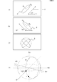
- FIG. 5A, FIG. 5B, FIG. 5C, and FIG. 5D are diagrams for explaining the principle of optical compensation. It is a figure showing the transmitted light intensity in each wavelength.
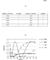
- FIG. 7A is a diagram showing the result of evaluating the change in color of the image with respect to the optimum retardation, and
- FIG. 7B is a diagram showing the transmitted light intensity at each wavelength.
- 11 is a side cross-sectional view of a display device according to Modification 1.
- FIG. 10 is a side cross-sectional view of a display device according to Modification 2.
- FIG. 10 is a side cross-sectional view of a display device according to Modification 2.
- FIG. 14 is a side cross-sectional view of a display device according to Modification 3.
- FIG. It is a figure which shows the relationship of a slow axis.
- the display device 1 includes a rectangular parallelepiped housing 50 and a planar surface panel 40 disposed in an opening on the upper surface of the housing 50 in appearance. Yes.
- the front panel 40 functions as an operation surface on which a user performs a touch operation using a finger, a pen, or the like.
- the width direction (lateral direction) of the casing 50 is the X direction
- the length direction (vertical direction) is the Y direction
- the thickness direction is the Z direction.
- the piezoelectric sensor 11 and the display panel 30 are arranged inside the housing 50 along the Z direction in order from the opening (surface panel 40) side of the housing 50.
- the front panel 40 and the piezoelectric sensor 11 constitute a touch panel.
- the piezoelectric sensor 11 and the display panel 30 have a flat plate shape, and are arranged inside the housing 50 so as to face the opening (surface panel 40) of the housing 50, respectively.
- a circuit board (not shown) is disposed between the bottom surface of the housing 50 and the display panel 30.
- the circuit board is provided with a circuit module constituting the detection unit 20 shown in FIG.
- the piezoelectric sensor 11 and the processing unit 22 are connected to the detection unit 20.
- the detection unit 20, the program storage unit 23, and the display panel 30 are connected to the processing unit 22.
- the display device 1 includes a touch input device 45 and a processing device 47.
- the piezoelectric sensor 11 and the detection unit 20 constitute a touch input device 45.
- the processing unit 22, the program storage unit 23, and the display panel 30 constitute a processing device 47.
- the processing unit 22 includes a CPU and controls the processing device 47 in an integrated manner. That is, the processing unit 22 reads the operation program stored in the program storage unit 23 and performs various processes. For example, the processing unit 22 controls the display panel 30 to display an image, determines the operation input content according to the detection signal input from the detection unit 20, and changes the displayed image.
- the piezoelectric sensor 11 generates a charge corresponding to a pressing operation on the surface panel 40 that is an operation surface.
- the detection unit 20 detects the electric charge generated by the piezoelectric sensor 11 and outputs it to the processing unit 22 as a detection signal.
- the display panel 30 is made of, for example, a liquid crystal display element.
- the display panel 30 includes a front polarizing plate 301, a liquid crystal panel 302, a back polarizing plate 303, and a backlight 304.
- the front polarizing plate 301 and the back polarizing plate 303 are arranged so as to sandwich the liquid crystal panel 302.
- the backlight 304 is disposed on the opposite side of the liquid crystal panel 302 with the back polarizing plate 303 interposed therebetween.
- the polarization direction L3 of the front polarizing plate 301 is 75 ° with respect to the X axis
- the polarization direction L4 of the back polarizing plate 303 is 165 °.
- the light output from the backlight 304 is polarized by the back polarizing plate 303 and reaches the front polarizing plate 301 through the liquid crystal panel 302.
- the liquid crystal panel 302 changes the amount of light passing through the front polarizing plate 302 for each pixel under the control of the processing unit 22.
- the light output from the front polarizing plate 302 is output to the front panel 40 via the piezoelectric sensor 11. As a result, various images are displayed on the front panel 40.
- the piezoelectric sensor 11 includes a first electrode film 111, a first electrode 112, a piezoelectric sheet 113, a second electrode 114, and a second electrode film 115 in order from the surface side.
- the first electrode 112 and the second electrode 114 are disposed so as to cover substantially the entire main surface of the piezoelectric sheet 113.
- the first electrode 112 and the second electrode 114 are made of a transparent material, for example, a material mainly composed of indium tin oxide (ITO), zinc oxide (ZnO), or polythiophene.
- the first electrode 112 and the second electrode 114 are respectively formed in advance on the main surfaces of the first electrode film 111 and the second electrode film 115 by vapor deposition or the like.
- the piezoelectric sheet 113 has one main surface (the main surface on the front side) attached to the front panel 40.
- the piezoelectric sheet 113 is bent in the normal direction when the user presses the front panel 40 to generate electric charges.
- the piezoelectric sheet 113 can use a material such as PVDF, but it is preferable to use a highly transparent chiral polymer. More preferably, the piezoelectric sheet 113 is preferably uniaxially stretched polylactic acid (PLA), and more preferably L-type polylactic acid (PLLA).
- Chiral polymers have a helical structure in the main chain and have piezoelectricity when the molecules are oriented uniaxially.
- the amount of charge generated by the uniaxially stretched chiral polymer is uniquely determined by the amount of displacement of the front panel 40 in the normal direction.
- the piezoelectric constant of uniaxially stretched PLLA belongs to a very high class among polymers. That is, it is possible to detect a pressing operation with high sensitivity and to output a deformation detection signal corresponding to the pressing amount with high accuracy.
- chiral polymers do not need to be subjected to poling treatment because piezoelectricity is generated by molecular orientation treatment such as stretching.
- polylactic acid does not have pyroelectricity, and therefore, even when a piezoelectric sensor is disposed near the operation surface and heat from a user's finger or the like is transmitted, the detected charge amount may change. Absent.
- the piezoelectric constant of PLLA does not vary with time and is extremely stable.
- the piezoelectric sheet 113 is arranged such that the uniaxial stretching direction L1 forms an angle of approximately 45 ° with respect to the X direction and the Y direction.
- the draw ratio is preferably about 3 to 8 times.
- the same effect as uniaxial stretching can be obtained by varying the stretching ratio of each axis. For example, when a certain direction is set as the X-axis, the uniaxial stretching is performed about 4 times in the X-axis direction when the X-axis direction is 8 times and the Y-axis direction orthogonal to the X-axis is doubled. The same effect as the case can be obtained.
- a film that is simply uniaxially stretched easily tears along the direction of the stretch axis, and thus the strength can be increased somewhat by performing biaxial stretching as described above.
- the first electrode film 111 is an example of the optical compensation layer of the present invention.
- the first electrode film 111 has an in-plane retardation. As shown in FIG. 4, the slow axis L ⁇ b> 2 of the first electrode film 111 is orthogonal to the stretching direction of the piezoelectric sheet 113. Thereby, the phase difference in the first electrode film 111 and the phase difference in the piezoelectric sheet 113 are canceled out.
- FIG. 5 is a diagram for explaining the principle of optical compensation.
- the extending direction L1 of the piezoelectric sheet 113 is 45 ° with respect to the X axis. Therefore, the major axis of the refractive index ellipsoid P showing the in-plane phase difference of the piezoelectric sheet 113 is 45 ° with respect to the X axis.
- the retardation Re of the piezoelectric sheet 113 is 1000 nm.
- the slow axis L2 of the first electrode film 111 is disposed so as to be orthogonal to the stretching direction L1 of the piezoelectric sheet 113. Therefore, the major axis of the refractive index ellipsoid E is 135 ° with respect to the X axis.
- the piezoelectric sheet 113 and the first electrode film 111 are overlapped, the refractive index ellipsoid P and the refractive index ellipsoid E are combined so as to cancel each other. It becomes equivalent. Therefore, the piezoelectric sheet 113 and the first electrode film 111 are equivalent to a medium having an isotropic refractive index sphere S and do not give a phase difference to light.
- FIG. 5D is a diagram showing the locus of the polarization state on the Poincare sphere when the light emitted from the front polarizing plate 301 passes through the piezoelectric sheet 113 and the first electrode film 111.
- the polarization state of the light emitted from the front polarizing plate 301 is located at P0 on the S1 axis of the Poincare sphere.
- the polarization state of the light rotates along the locus R1 based on the retardation Re of the piezoelectric sheet 113 with A1 (30 ° ⁇ 2) as the rotation axis.
- A1 (30 ° ⁇ 2) as the rotation axis.
- 30 ° which determines the rotation axis of A1 is an angle formed by L1 and L3 as seen from the traveling direction of the light beam.
- the polarization state of the light reaches the position P1 on the Poincare sphere.
- the polarization state of the light rotates about A2 (120 ° ⁇ 2).
- 120 ° which determines the rotation axis of A2 is an angle formed by L2 and L3 as seen from the traveling direction of the light beam.
- the rotation axis A1 and the rotation axis A2 are shifted by 180 degrees, and the retardation Re of the first electrode film 111 is equal to the retardation Re of the piezoelectric sheet 113. Therefore, the polarization state of the light rotates so as to reverse the locus R1 from the position of the polarization state P1. Therefore, the polarization state P2 after passing through the first electrode film 111 is at the same position as the polarization state P0.
- the polarization direction of the front polarizing plate 301 is preferably orthogonal or parallel to the stretching direction of the piezoelectric sheet 113.
- the polarization direction L3 of the front polarizing plate 301 and the polarization direction L4 of the back polarizing plate 303 are due to manufacturing variations of the piezoelectric sensor 11, manufacturing variations of the display panel 30, or assembly variations between the piezoelectric sensor 11 and the display panel 30, etc. There may be deviation.
- the piezoelectric sheet stretching direction optimal for pressing detection and the polarization direction of the front polarizing plate of the display panel are not necessarily parallel or orthogonal. For example, as shown in FIG.
- the polarization direction L3 is 75 ° with respect to the X axis, and may not be orthogonal or parallel to the extending direction of the piezoelectric sheet.
- the piezoelectric sensor 11 of the present embodiment rotates in the opposite direction to the rotation from the polarization state P0 to the polarization state P1, and the rotation amount. Since they are the same depending on the wavelength, broadband optical compensation independent of the wavelength becomes possible.
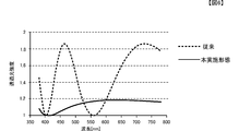
- FIG. 6 is a diagram showing transmitted light intensity at each wavelength.
- the “transmitted light intensity” on the vertical axis of the graph shown in FIG. 6 indicates the transmitted light intensity of polarized sunglasses whose polarization direction is shifted by 45 ° with respect to the polarization direction L3 of the front polarizing plate 301, and The ratio with respect to the transmitted light intensity when the polarization direction L3 of the front polarizing plate 301 matches is shown.
- the broken line in the figure indicates that the first electrode film 111 has no in-plane retardation when the polarization direction L3 of the front polarizing plate 301 is 75 ° with respect to the X axis (that is, when it is not optically compensated).
- the transmitted light intensity greatly changes depending on the wavelength, and the color of the image changes.
- the solid line in the figure indicates that the phase difference of the piezoelectric sheet 113 is canceled by the first electrode film 111 when the polarization direction L3 of the front polarizing plate 301 is 75 ° with respect to the X axis (that is, optically).
- the intensity of transmitted light in the case of compensation). In this case, the change in transmitted light intensity at each wavelength is reduced, and the change in the color of the image is suppressed.
- the slow axis L2 of the first electrode film 111 is orthogonal to the stretching direction L1 of the piezoelectric sheet 113 and the retardation is the same, but the retardation of the second electrode film 115 is the same.
- the phase axis may be orthogonal to the stretching direction L1 of the piezoelectric sheet 113 and the retardation may be the same. That is, it is sufficient that at least one of the first electrode film 111 and the second electrode film 115 compensates for the in-plane retardation of the piezoelectric sheet 113.
- a dielectric sheet different from the first electrode film 111 and the second electrode film 115 may be provided, and the dielectric sheet may compensate the in-plane retardation of the piezoelectric sheet 113.
- the slow axis of the first electrode film 111 or the second electrode film 115 is accurately orthogonal to the stretching direction of the piezoelectric sheet 113, and a deviation of ⁇ 5 ° is acceptable. It is. Also, the retardation value need not be the same.
- the display image is viewed with polarized sunglasses.
- the retardation of the film for 1st electrodes or the film for 2nd electrodes becomes + 40% with respect to optimal retardation, as shown to FIG. 7 (B), as shown in FIG.
- the intensity of the wavelength increases. In this case, although the change in the intensity ratio is small, since the visibility of green is high, a change in color is observed.
- the retardation of the first electrode film or the second electrode film is -40% with respect to the optimum retardation, the intensity of the red wavelength is remarkably increased with respect to the blue wavelength. Is strongly observed. Accordingly, the retardation of the film for the first electrode or the film for the second electrode may be + 40% to ⁇ 30%, more preferably within ⁇ 30% with respect to the optimum retardation.
- FIG. 8 is a side sectional view of the display device 1A according to the first modification. Components that are the same as those in FIG. 2 are given the same reference numerals, and descriptions thereof are omitted.
- the display device 1 ⁇ / b> A includes a capacitance sensor 70 in addition to the configuration of the display device 1.
- the electrostatic capacity sensor 70 is disposed closer to the front panel 40 than the piezoelectric sensor 11. That is, each component is arranged in the order of the electrostatic capacity sensor 70, the piezoelectric sensor 11, and the display panel 30 along the Z direction in order from the opening (front panel 40) side of the housing 50.
- the electrostatic capacitance sensor 70 has a flat plate shape and is arranged inside the housing 50 so as to be parallel to the opening (surface panel 40) of the housing 50.
- the capacitance sensor 70 includes a first capacitance detection electrode 701, a flat insulating substrate 702, and a second capacitance detection electrode 703.
- the insulating substrate 702 is made of a material having transparency, for example, PMMA (acrylic resin).
- a first capacitance detection electrode 701 is formed on the main surface on the front surface side of the insulating substrate 702, and a second capacitance detection electrode 703 is disposed on the main surface on the back surface side.
- the first capacitance detection electrode 701 and the second capacitance detection electrode 703 are all made of a transparent material, for example, containing indium tin oxide (ITO), zinc oxide (ZnO), and polythiophene as main components. Use materials.
- ITO indium tin oxide
- ZnO zinc oxide
- polythiophene polythiophene
- the capacitance sensor 70 detects the presence / absence of a touch operation and the touch position based on changes in capacitance detected by the first capacitance detection electrode 701 and the second capacitance detection electrode 703.
- the first electrode film 111 of the piezoelectric sensor 11 and the second capacitance detection electrode 703 of the capacitance sensor 70 are arranged on the same surface. That is, the first electrode film 111 is provided with the first electrodes 112 and the second capacitance detection electrodes 703 so as to be alternately arranged in parallel.
- the display device 1A according to the modified example 1 can reduce the total number of films by providing a part of the electrodes of the capacitance sensor and a part of the electrodes of the piezoelectric sensor on the same film. it can.
- FIG. 9 is a side sectional view of the display device 1B according to the second modification.
- FIG. 10 is a diagram illustrating the relationship of the slow axes of the display device 1B according to the second modification.
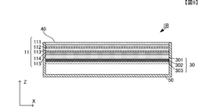
- the display device 1B according to the modification 2 is the same as the display device 1 shown in FIG. 2 in the configuration shown in FIG.
- the first electrode film 111 has an in-plane retardation, and the slow axis L2 of the first electrode film 111 is approximately 45 ° with respect to the polarization direction L3 of the front polarizing plate 301. It has become.
- the retardation of the first electrode film 111 is ⁇ / 4 with respect to the light wavelength ⁇ .
- the second electrode film 115 of the display device 1B has an in-plane retardation, and the slow axis L5 of the second electrode film 115 is approximately 90 ° with respect to the stretching direction L1 of the piezoelectric sheet 113. ing.
- the polarization state of the light emitted from the front polarizing plate 301 is located at P0.
- the polarization state when passing through the second electrode film 115 is rotated along the locus R2 based on the retardation of the second electrode film 115 with A1 (120 ° ⁇ 2) as the rotation axis, and P1 To reach the position.
- 120 ° which determines the rotation axis of A1 is an angle formed by L3 and L5 as seen from the traveling direction of the light beam.
- the polarization state when passing through the piezoelectric sheet 113 rotates based on the retardation of the piezoelectric sheet 113 with A2 (30 ° ⁇ 2) as an axis.
- 30 ° which determines the rotation axis of A2 is an angle formed by L3 and L1 as seen from the traveling direction of the light beam.
- the retardation of the second electrode film 115 is equal to the retardation of the piezoelectric sheet 113, the second electrode film 115 rotates so as to reverse the trajectory R2 from P1. Therefore, the polarization state P2 after passing through the piezoelectric sheet 113 is at the same position as P0.
- the polarization state when passing through the first electrode film 111 is rotated along the locus R3 based on the retardation of the first electrode film 111 with A3 (45 ° ⁇ 2) as the rotation axis, and the position of P3 To reach. 45 ° which determines the rotation axis of A3 is an angle formed by L3 and L2 as seen from the traveling direction of the light beam.
- the position P3 exists on the S3 axis in the Poincare sphere. Therefore, the light that has passed through the first electrode film 111 is in a circularly polarized state. Therefore, even when the polarization direction of the front polarizing plate 301 and the polarization direction of the polarized sunglasses are orthogonal, the light is transmitted without being blacked out and the image can be visually recognized.
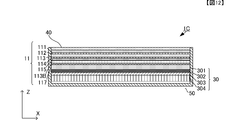
- FIG. 12 is a side cross-sectional view of a display device 1C according to Modification 3. Components that are the same as those in FIG. 2 are given the same reference numerals, and descriptions thereof are omitted.
- the display device 1 ⁇ / b> C further includes an optical compensation piezoelectric sheet 113 ⁇ / b> B extended in a uniaxial direction and a third electrode 117.
- the first electrode film 111 of the display device 1 does not have an in-plane retardation.
- the optical compensation piezoelectric sheet 113 ⁇ / b> B is disposed closer to the display panel 30 than the first electrode film 111.
- the third electrode 117 is also made of a transparent material, for example, a material mainly composed of indium tin oxide (ITO), zinc oxide (ZnO), and polythiophene.
- the third electrode 117 is formed in advance on the main surface of the second electrode film 115 by vapor deposition or the like.
- the second electrode 114 functions as a ground electrode.
- the first electrode 112 functions as a detection electrode of the piezoelectric sheet 113.
- the third electrode 117 functions as a detection electrode of the optical compensation piezoelectric sheet 113B.
- the piezoelectric sheet 113 is arranged such that the uniaxial stretching direction L1 forms an angle of about 45 ° with respect to the X direction and the Y direction.
- the optical compensation piezoelectric sheet 113B is an example of the optical compensation layer of the present invention.
- the optical compensation piezoelectric sheet 113B has an in-plane retardation. As shown in FIG. 13, the uniaxial stretching direction L6 of the optical compensation piezoelectric sheet 113B is orthogonal to the uniaxial stretching direction L1 of the piezoelectric sheet 113. As a result, the phase difference in the optical compensation piezoelectric sheet 113B and the phase difference in the piezoelectric sheet 113 are canceled out.
- the principle of optical compensation is the same as in the first embodiment.
- the configuration of the modification 3 further includes the optical compensation piezoelectric sheet 113B, so that a deformation detection signal corresponding to the pressing amount is increased, and the pressing operation can be detected with higher sensitivity.
- the piezoelectric sheet 113 and the optical compensation piezoelectric sheet 113B are made of the same material (for example, PLLA), it is not necessary to separately manufacture a film for optical compensation.
- the uniaxial stretching direction L6 of the optical compensation piezoelectric sheet 113B is not necessarily perpendicular to the uniaxial stretching direction L1 of the piezoelectric sheet 113. For example, even if it is deviated by ⁇ 5 °, the optical compensation is performed. Function is secured.
Landscapes
- Physics & Mathematics (AREA)
- Engineering & Computer Science (AREA)
- Nonlinear Science (AREA)
- General Physics & Mathematics (AREA)
- General Engineering & Computer Science (AREA)
- Theoretical Computer Science (AREA)
- Optics & Photonics (AREA)
- Crystallography & Structural Chemistry (AREA)
- Chemical & Material Sciences (AREA)
- Mathematical Physics (AREA)
- Human Computer Interaction (AREA)
- Spectroscopy & Molecular Physics (AREA)
- Polarising Elements (AREA)
- Liquid Crystal (AREA)
- Devices For Indicating Variable Information By Combining Individual Elements (AREA)
- Position Input By Displaying (AREA)
- Mechanical Light Control Or Optical Switches (AREA)
Abstract
圧電センサは、一軸方向に延伸された圧電シートと、前記圧電シートに発生する電荷を検出する電極と、前記圧電シートの少なくとも一方側に積層され、前記一軸方向に対して交差する遅相軸を有し、前記圧電シートが一軸方向に延伸されることにより生じる位相差を光学的に補償する光学補償層と、を備えている。
Description
本発明は、圧電センサ、当該圧電センサを備えたタッチパネル、タッチ式入力装置、および表示装置に関する。
特許文献1には、操作面(最外面)に表面偏光板が配置された表示パネルが開示されている。特許文献1の表示パネルは、表面偏光板の操作面と反対側の面に、タッチパネルが配置されている。また、タッチパネルのうち、表面偏光板と反対側には、液晶をはさみ込んだ一対のガラスからなる液晶パネルが配置されている。
一方、特許文献2には、一軸延伸された圧電シートを用いて押圧検出を行う表示装置が開示されている。
しかし、圧電シートは、一軸延伸されることにより複屈折性が生じる。したがって、例えば偏光サングラスを掛けて表示画像を見ると、圧電シートの位相差により光強度の波長特性が変化し、画像の色味が変化する。
光学特性は、例えば、表示パネルの表偏光板の偏光方向と、圧電シートの一軸延伸方向と、を平行または直交にすることで、圧電シートの位相差の影響を無くすことができる。
しかし、圧電センサの製造ばらつき、表示パネルの製造ばらつき、または圧電センサと表示パネルの組立ばらつき、等により、表示パネルの表偏光板の偏光方向と、圧電シートの延伸方向と、が平行または直交の状態からずれる場合がある。また、押圧検出に最適な圧電シートの延伸方向と表示パネルの表偏光板の偏光方向は必ずしも平行または直交の状態であるとは限らず、表示パネルの表偏光板の偏光方向と、圧電シートの延伸方向と、が平行または直交の状態からずれると、偏光サングラスを掛けて表示画像を見た時に、画像の色味が変化する。
そこで、本発明は、表示パネルの表偏光板の偏光方向と、圧電シートの延伸方向と、が平行または直交の状態からずれていても、偏光サングラスを掛けて表示画像を見た時に、画像の色味の変化を抑制することができる圧電センサ、タッチパネル、タッチ式入力装置、および表示装置を提供する。
本発明の圧電センサは、一軸方向に延伸された圧電シートと、前記圧電シートに発生する電荷を検出する電極と、前記圧電シートの少なくとも一方側に積層され、前記一軸方向に対して交差する遅相軸を有し、前記圧電シートが一軸方向に延伸されることにより生じる位相差を光学的に補償する光学補償層と、を備えている。
このように、圧電センサは、圧電シートの上面または下面に光学補償層を備えている。光学補償層は、遅相軸が圧電シートの延伸方向と交差していることにより、光学補償層における位相差と、圧電シートの位相差と、が相殺される。これにより、表示パネルの表偏光板の偏光方向と、圧電性フィルムの延伸方向と、が平行または直交の状態からずれていても、偏光サングラスを掛けて表示画像を見た時に、画像の色味の変化を抑制することができる。
なお、圧電シートは、PVDFであってもよいが、表示装置に用いるためには、透明性の高いキラル高分子を用いることが好ましい。より好ましくは、一軸延伸されたポリ乳酸(PLA)、さらにはL型ポリ乳酸(PLLA)であることが好ましい。
なお、電極は、電極用フィルムに形成され、当該電極用フィルムが、前記光学補償層となっていることにより、新たな層を設けることなく、光学補償層を形成することができる。
この発明によれば、表示パネルの表偏光板の偏光方向と、圧電性フィルムの延伸方向と、が平行または直交の状態からずれていても、偏光サングラスを掛けて表示画像を見た時に、画像の色味の変化を抑制することができる。
以下、図面を参照して、本発明の圧電センサを備えた表示装置について説明する。
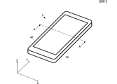
図1の外観斜視図に示すように、表示装置1は、外観上、直方体形状の筐体50と、筐体50の上面の開口部に配置された平面状の表面パネル40と、を備えている。表面パネル40は、利用者が指やペン等を用いてタッチ操作を行う操作面として機能する。
なお、本実施形態では、筐体50の幅方向(横方向)をX方向とし、長さ方向(縦方向)をY方向とし、厚み方向をZ方向とする。
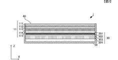
図2に示すように、筐体50の内部には、筐体50の開口部(表面パネル40)側から順にZ方向に沿って、圧電センサ11および表示パネル30が配置されている。表面パネル40および圧電センサ11によりタッチパネルが構成される。
圧電センサ11および表示パネル30は、平板状であり、それぞれ筐体50の開口部(表面パネル40)と対面するように、筐体50の内部に配置されている。
筐体50の底面と表示パネル30との間には、回路基板(不図示)が配置されている。当該回路基板には、図3に示す検出部20を構成する回路モジュールが設けられている。
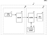
図3に示すように、検出部20には、圧電センサ11および処理部22が接続される。処理部22には、検出部20、プログラム記憶部23、および表示パネル30が接続される。
表示装置1は、タッチ式入力装置45および処理装置47からなる。圧電センサ11および検出部20は、タッチ式入力装置45を構成する。処理部22、プログラム記憶部23、および表示パネル30は、処理装置47を構成する。
処理部22は、CPUを含み、処理装置47を統括的に制御する。すなわち、処理部22は、プログラム記憶部23に記憶されている動作用プログラムを読み出して各種処理を行う。例えば、処理部22は、表示パネル30を制御して画像を表示させるとともに、検出部20から入力された検出信号に応じて操作入力内容を決定し、表示されている画像を変更する。
圧電センサ11は、操作面である表面パネル40に対する押圧操作に応じた電荷を発生する。検出部20は、圧電センサ11で発生した電荷を検出し、検出信号として処理部22に出力する。
表示パネル30は、例えば液晶表示素子からなる。この例では、図2に示すように、表示パネル30は、表偏光板301、液晶パネル302、裏偏光板303、およびバックライト304を備えている。
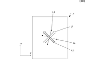
表偏光板301および裏偏光板303は、液晶パネル302を挟むように配置されている。バックライト304は、裏偏光板303を挟んで、液晶パネル302と反対側に配置されている。また、図4に示すように、表偏光板301の偏光方向L3はX軸に対して75°、裏偏光板303の偏光方向L4は165°である。
バックライト304から出力された光は、裏偏光板303で偏光され、液晶パネル302を経て表偏光板301に達する。液晶パネル302は、処理部22の制御に応じて画素毎に表偏光板302を通過する光量を変化させる。表偏光板302から出力された光は、圧電センサ11を経て表面パネル40に出力される。これにより、表面パネル40に各種画像が表示される。
圧電センサ11は、表面側から順に、第1電極用フィルム111、第1電極112、圧電シート113、第2電極114、および第2電極用フィルム115を備えている。第1電極112および第2電極114は、圧電シート113の主面の略全面を覆うように配置されている。
第1電極112および第2電極114は、透明性を有する材料からなり、例えば酸化インジウムスズ(ITO)、酸化亜鉛(ZnO)、ポリチオフェンを主成分とする材料を用いる。第1電極112および第2電極114は、それぞれ第1電極用フィルム111および第2電極用フィルム115主面に、蒸着等により予め形成されている。
圧電シート113は、一方の主面(表面側の主面)が表面パネル40に貼り付けられている。圧電シート113は、利用者が表面パネル40を押圧することで法線方向に撓み、電荷を発生する。圧電シート113は、PVDF等の材料を用いることが可能であるが、透明性の高いキラル高分子を用いることが好ましい。より好ましくは、圧電シート113には、一軸延伸されたポリ乳酸(PLA)、さらにはL型ポリ乳酸(PLLA)であることが好ましい。
キラル高分子は、主鎖が螺旋構造を有し、一軸延伸されて分子が配向すると、圧電性を有する。そして、一軸延伸されたキラル高分子が発生する電荷量は、表面パネル40が法線方向へ変位する変位量によって一意的に決定される。
一軸延伸されたPLLAの圧電定数は、高分子中で非常に高い部類に属する。すなわち、押圧操作を高感度に検出し、押圧量に応じた変形検出信号を高精度に出力することができる。
また、キラル高分子は、延伸等による分子の配向処理で圧電性が生じるため、ポーリング処理を行う必要がない。特に、ポリ乳酸は、焦電性がないため、操作面に近い位置に圧電センサを配置し、利用者の指等の熱が伝わる場合であっても、検出される電荷量が変化することがない。さらに、PLLAの圧電定数は経時的に変動することがなく、極めて安定している。
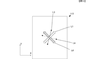
本実施形態では、図4に示すように、圧電シート113は、X方向およびY方向に対して、一軸延伸方向L1が略45°の角度を成すように配置されている。このような配置を行うことで、より高感度に押圧操作を検出できる。
なお、延伸倍率は3~8倍程度が好適である。延伸後に熱処理を施すことにより、ポリ乳酸の延びきり鎖結晶の結晶化が促進され圧電定数が向上する。また、二軸延伸した場合はそれぞれの軸の延伸倍率を異ならせることによって一軸延伸と同様の効果を得ることが出来る。例えば、ある方向をX軸としてX軸方向に8倍、X軸に直交するY軸方向に2倍の延伸を施した場合、圧電定数に関してはおよそX軸方向に4倍の一軸延伸を施した場合とほぼ同等の効果が得られる。単純に一軸延伸したフィルムは延伸軸方向に沿って裂け易いため、前述したような二軸延伸を行うことにより幾分強度を増すことができる。
第1電極用フィルム111は、本発明の光学補償層の一例である。第1電極用フィルム111は、面内位相差を有する。図4に示すように、第1電極用フィルム111の遅相軸L2は、圧電シート113の延伸方向と直交している。これにより、第1電極用フィルム111における位相差と、圧電シート113の位相差と、が相殺される。
図5は、光学補償原理を説明する図である。まず、図5(A)に示すように、圧電シート113の延伸方向L1は、X軸に対して45°である。したがって、圧電シート113の面内位相差を示す屈折率楕円体Pの長軸は、X軸に対して45°となる。また、圧電シート113のリタデーションReは、通常光線に対する屈折率noおよび異常光線に対する屈折率neにより、Re=(ne-no)×dで表される。ここで、例えば、屈折率noが1.45であり、屈折率neが1.47であり、圧電シート113の厚みd=50μmとすると、圧電シート113のリタデーションReは、1000nmとなる。
一方、図5(B)に示すように、第1電極用フィルム111の遅相軸L2は、圧電シート113の延伸方向L1と直交となるように配置されている。したがって、屈折率楕円体Eの長軸は、X軸に対して135°となる。第1電極用フィルム111のリタデーションReは、例えば通常光線に対する屈折率Noが1.7であり、異常光線に対する屈折率Neが1.725であり、厚みD=40μmとすると、Re=(Ne-No)×Dにより、1000nmとなる。
したがって、図5(C)に示すように、圧電シート113と第1電極用フィルム111とを重ね合わせると、屈折率楕円体Pと屈折率楕円体Eが互いに相殺するように合成されたものと等価となる。よって、圧電シート113および第1電極用フィルム111は、等方的な屈折率球Sを持つ媒体と等価なものとなり、光に対して位相差を与えなくなる。
次に、図5(D)を参照して、光の偏光状態の変化について説明する。図5(D)は、表偏光板301から出た光が圧電シート113および第1電極用フィルム111を通過するときの偏光状態の軌跡をポアンカレ球上で示した図である。
図5(D)において、表偏光板301から出た光の偏光状態は、ポアンカレ球のS1軸上のP0に位置する。ここで、光の偏光状態は、圧電シート113を通過するとき、A1(30°×2)を回転軸として、圧電シート113のリタデーションReに基づいて軌跡R1に沿って回転する。A1の回転軸を決める30°は、光線の進行方向から見たL1とL3の成す角である。これにより、光の偏光状態は、ポアンカレ球上のP1の位置に到達する。
次に、第1電極用フィルム111を通過するとき、光の偏光状態は、A2(120°×2)を軸として回転する。A2の回転軸を決める120°は、光線の進行方向から見たL2とL3の成す角である。このとき、回転軸A1と回転軸A2とは、180度のずれがあり、かつ第1電極用フィルム111のリタデーションReは、圧電シート113のリタデーションReに等しい。したがって、光の偏光状態は、偏光状態P1の位置から軌跡R1を逆戻りするように回転する。したがって、第1電極用フィルム111を通過した後の偏光状態P2は、偏光状態P0と同じ位置となる。
表偏光板301の偏光方向は、理想的には圧電シート113の延伸方向に対して直交または平行となることが好ましい。しかし、表偏光板301の偏光方向L3および裏偏光板303の偏光方向L4は、圧電センサ11の製造ばらつき、表示パネル30の製造ばらつき、または圧電センサ11と表示パネル30の組立ばらつき、等により、ずれる場合がある。また、押圧検出に最適な圧電シートの延伸方向と表示パネルの表偏光板の偏光方向は必ずしも平行または直交の状態であるとは限らず、例えば、図4に示すように、表偏光板301の偏光方向L3がX軸に対して75°となり、圧電シートの延伸方向と直交または平行とならない場合がある。この場合、光が圧電シート113を通過するとき、偏光状態P1の位置にずれ、光の波長によっては軌跡R1上のP1とは異なる位置に変化する。しかし、本実施形態の圧電センサ11は、光が第1電極用フィルム111を通過するとき、偏光状態P0の位置から偏光状態P1の位置に回転したときとは逆方向に回転し、かつ回転量が波長によって同一となるため、波長に依存しない広帯域な光学補償が可能になる。
図6は、各波長における透過光強度を表した図である。同図に示すグラフの縦軸の「透過光強度」は、表偏光板301の偏光方向L3に対する偏光方向が45°ずれた偏光サングラスの透過光強度を示し、かつ圧電シート113の延伸方向L1と、表偏光板301の偏光方向L3が一致しているときの透過光強度に対する比を表すものである。
図中の破線は、表偏光板301の偏光方向L3がX軸に対して75°である場合に、第1電極用フィルム111に面内位相差がない場合(すなわち光学的に補償されない場合)の透過光強度である。このように、光学的に補償されていない場合、透過光強度は、波長によって大きく変化し、画像の色味が変化してしまう。
一方、図中の実線は、表偏光板301の偏光方向L3がX軸に対して75°である場合に、第1電極用フィルム111で圧電シート113の位相差が相殺される(すなわち光学的に補償される)場合の透過光強度である。この場合、各波長での透過光強度の変化が少なくなり、画像の色味の変化は抑制される。
なお、上述の例では、第1電極用フィルム111の遅相軸L2が圧電シート113の延伸方向L1と直交し、かつリタデーションが同一である例を示したが、第2電極用フィルム115の遅相軸と圧電シート113の延伸方向L1と直交し、かつリタデーションが同一である態様であってもよい。すなわち、第1電極用フィルム111または第2電極用フィルム115の少なくともいずれか一方が圧電シート113の面内位相差を補償する態様であればよい。あるいは、第1電極用フィルム111および第2電極用フィルム115とは別の誘電体シートを設けて、当該誘電体シートが、圧電シート113の面内位相差を補償する態様であってもよい。
また、第1電極用フィルム111または第2電極用フィルム115の遅相軸は、圧電シート113の延伸方向に対して正確に直交していることは必須ではなく、±5°のずれは許容範囲である。また、リタデーションの値も、同一である必要はない。
例えば、図7(A)に示すように、最適なリタデーションに対して、第1電極用フィルムまたは第2電極用フィルムのリタデーションが±30%以内であれば、偏光サングラスを掛けて表示画像を見た時の色味の変化は実用上問題がない。なお、最適なリタデーションに対して、第1電極用フィルムまたは第2電極用フィルムのリタデーションが+40%となると、図7(B)に示すように、緑色の波長に対して青の波長および赤の波長の強度が大きくなる。この場合、強度比の変化は少ないものの、緑色は、視感度が高いため色味の変化が観測されてしまう。逆に、最適なリタデーションに対して第1電極用フィルムまたは第2電極用フィルムのリタデーションが-40%となると、青の波長に対して赤の波長の強度が著しく大きくなるため、色味の変化が強く観測されてしまう。したがって、第1電極用フィルムまたは第2電極用フィルムのリタデーションは最適なリタデーションに対して+40%~-30%であればよく、より好ましくは±30%以内であればよい。
次に、図8は、変形例1に係る表示装置1Aの側面断面図である。図2と共通する構成については同一の符号を付し、説明を省略する。
表示装置1Aは、表示装置1の構成に加えて、静電容量センサ70を備えている。静電容量センサ70は、圧電センサ11よりも表面パネル40側に配置されている。すなわち、各構成部は、筐体50の開口部(表面パネル40)側から順にZ方向に沿って、静電容量センサ70、圧電センサ11、および表示パネル30の順で配置される。
静電容量センサ70は、平板状であり、筐体50の開口部(表面パネル40)と平行になるように、筐体50の内部に配置されている。
静電容量センサ70は、第1静電容量検出用電極701、平板状の絶縁性基板702、および第2静電容量検出用電極703を備えている。絶縁性基板702は、透明性を有する材料からなり、例えばPMMA(アクリル樹脂)からなる。絶縁性基板702の表面側の主面には、第1静電容量検出用電極701が形成され、裏面側の主面には、第2静電容量検出用電極703が配置されている。
第1静電容量検出用電極701および第2静電容量検出用電極703は、全て透明性を有する材料からなり、例えば酸化インジウムスズ(ITO)、酸化亜鉛(ZnO)、ポリチオフェンを主成分とする材料を用いる。
静電容量センサ70は、第1静電容量検出用電極701および第2静電容量検出用電極703で検出される静電容量の変化により、タッチ操作の有無およびタッチ位置を検出する。
そして、圧電センサ11の第1電極用フィルム111および静電容量センサ70の第2静電容量検出用電極703は、同じ面上に配置されている。すなわち、第1電極用フィルム111には、第1電極112および第2静電容量検出用電極703が、交互に並行するように設けられている。このように、変形例1に係る表示装置1Aは、静電容量センサの電極の一部と、圧電センサの電極の一部とを同一のフィルム上に設けることにより、フィルムの総数を減らすことができる。
次に、図9は、変形例2に係る表示装置1Bの側面断面図である。図10は、変形例2に係る表示装置1Bの遅相軸の関係を示す図である。
変形例2に係る表示装置1Bは、図9に示す構成上では、図2に示した表示装置1と同じである。しかし、表示装置1Bでは、第1電極用フィルム111は、面内位相差があり、かつ第1電極用フィルム111の遅相軸L2は、表偏光板301の偏光方向L3に対して略45°となっている。また、第1電極用フィルム111のリタデーションは光の波長λに対してλ/4となっている。また、表示装置1Bの第2電極用フィルム115は、面内位相差があり、かつ第2電極用フィルム115の遅相軸L5は、圧電シート113の延伸方向L1に対して略90°となっている。
図11を参照して、光の偏光状態の変化について説明する。図11のポアンカレ球に示すように、表偏光板301から出た光の偏光状態は、P0に位置する。ここで、第2電極用フィルム115を通過するときの偏光状態は、A1(120°×2)を回転軸として、第2電極用フィルム115のリタデーションに基づいて軌跡R2に沿って回転し、P1の位置に到達する。A1の回転軸を決める120°は、光線の進行方向から見たL3とL5の成す角である。次に、圧電シート113を通過するときの偏光状態は、A2(30°×2)を軸として圧電シート113のリタデーションに基づいて回転する。A2の回転軸を決める30°は、光線の進行方向から見たL3とL1の成す角である。このとき、第2電極用フィルム115のリタデーションと、圧電シート113のリタデーションが等しいため、P1から軌跡R2を逆戻りするように回転する。したがって、圧電シート113を通過した後の偏光状態P2は、P0と同じ位置となる。
さらに、第1電極用フィルム111を通過するときの偏光状態は、A3(45°×2)を回転軸として、第1電極用フィルム111のリタデーションに基づき軌跡R3に沿って回転し、P3の位置に到達する。A3の回転軸を決める45°は、光線の進行方向から見たL3とL2の成す角である。
位置P3は、ポアンカレ球におけるS3軸上に存在する。したがって、第1電極用フィルム111を通過した光は、円偏光状態になる。そのため、表偏光板301の偏光方向と偏光サングラスの偏光方向が直交した場合でもブラックアウトすることなく光が透過し、画像を視認することができる。
次に、図12は、変形例3に係る表示装置1Cの側面断面図である。図2と共通する構成については同一の符号を付し、説明を省略する。
表示装置1Cは、表示装置1の構成に加えて、一軸方向に延伸された光学補償用圧電シート113Bと、第3電極117と、をさらに備えている。この場合、表示装置1の第1電極用フィルム111は、面内位相差を有していない。光学補償用圧電シート113Bは、第1電極用フィルム111よりも表示パネル30側に配置されている。
第3電極117も、透明性を有する材料からなり、例えば酸化インジウムスズ(ITO)、酸化亜鉛(ZnO)、ポリチオフェンを主成分とする材料を用いる。第3電極117は、第2電極用フィルム115主面に、蒸着等により予め形成されている。
変形例3では、第2電極114は、グランド電極として機能する。第1電極112は、圧電シート113の検知用電極として機能する。第3電極117は、光学補償用圧電シート113Bの検知用電極として機能する。
変形例3では、図13に示すように、圧電シート113は、X方向およびY方向に対して、一軸延伸方向L1が略45°の角度を成すように配置されている。
光学補償用圧電シート113Bは、本発明の光学補償層の一例である。光学補償用圧電シート113Bは、面内位相差を有する。図13に示すように、光学補償用圧電シート113Bの一軸延伸方向L6は、圧電シート113の一軸延伸方向L1と直交している。これにより、光学補償用圧電シート113Bにおける位相差と、圧電シート113の位相差と、が相殺される。光学補償の原理は、第1実施形態と同様である。
このように、変形例3の構成は、光学補償用圧電シート113Bをさらに備えることで、押圧量に応じた変形検出信号が大きくなり、より押圧操作を高感度に検出することができる。また、変形例3において、圧電シート113と光学補償用圧電シート113Bとを同じ材料(例えばPLLA)で構成すれば、光学補償のためのフィルムを別途製造する必要がなくなる。なお、光学補償用圧電シート113Bの一軸延伸方向L6は、圧電シート113の一軸延伸方向L1に対して正確に直交していることは必須ではなく、例えば±5°ずれたとしても、光学補償の機能は確保される。
1,1A,1B…表示装置
11…圧電センサ
20…検出部
22…処理部
23…プログラム記憶部
30…表示パネル
40…表面パネル
45…タッチ式入力装置
47…処理装置
50…筐体
70…静電容量センサ
111…第1電極用フィルム
112…第1電極
113…圧電シート
113B…光学補償用圧電シート
114…第2電極
115…第2電極用フィルム
117…第3電極
301…表偏光板
302…液晶パネル
303…裏偏光板
304…バックライト
11…圧電センサ
20…検出部
22…処理部
23…プログラム記憶部
30…表示パネル
40…表面パネル
45…タッチ式入力装置
47…処理装置
50…筐体
70…静電容量センサ
111…第1電極用フィルム
112…第1電極
113…圧電シート
113B…光学補償用圧電シート
114…第2電極
115…第2電極用フィルム
117…第3電極
301…表偏光板
302…液晶パネル
303…裏偏光板
304…バックライト
Claims (11)
- 一軸方向に延伸された圧電シートと、
前記圧電シートに発生する電荷を検出する電極と、
前記圧電シートの少なくとも一方側に配置され、前記一軸方向に対して交差する遅相軸を有し、前記圧電シートが一軸方向に延伸されることにより生じる位相差を光学的に補償する光学補償層と、
を備える圧電センサ。 - 前記光学補償層のリタデーション値は、前記圧電シートのリタデーション値に対して40%~-30%の範囲内である請求項1に記載の圧電センサ。
- 前記光学補償層のリタデーション値は、圧電シートのリタデーション値に対して±30%の範囲内である請求項1に記載の圧電センサ。
- 前記遅相軸は、前記一軸方向に直交する請求項1乃至請求項3のいずれかに記載の圧電センサ。
- 前記圧電シートは、ポリ乳酸を含む請求項1乃至請求項4のいずれかに記載の圧電センサ。
- 前記電極は、電極用フィルムに形成され、
当該電極用フィルムが、前記光学補償層となっている請求項1乃至請求項5のいずれかに記載の圧電センサ。 - 請求項1乃至請求項6のいずれかに記載の圧電センサと、
操作面と、
を備えたタッチパネル。 - 請求項7に記載のタッチパネルと、
前記操作面に対する押圧操作により、前記圧電センサに発生する電荷を検出する検出部と、
を備えたタッチ式入力装置。 - 請求項7に記載のタッチパネルと、
表示パネルと、
を備えた表示装置であって、
前記表示パネルは、前記操作面側に出射する光を制御することで表示画像を形成し、
前記表示パネルよりも前記操作面側に配置された表偏光板を備えた表示装置。 - 前記光学補償層の反対側に前記圧電フィルムを挟むように第2光学補償層が配置され、
前記第2光学補償層は、前記表偏光板の偏光方向と45度となる遅相軸を有する請求項9に記載の表示装置。 - 一軸方向に延伸された圧電シートと、
前記圧電シートに発生する電荷を検出する電極と、
前記圧電シートの少なくとも一方側に配置され、前記一軸方向に対して交差する遅相軸を有し、前記圧電シートのリタデーション値に対して±30%の範囲内であるリタデーション値を有する光学補償層と、を備える圧電センサ。
Priority Applications (3)
| Application Number | Priority Date | Filing Date | Title |
|---|---|---|---|
| JP2017528697A JP6332563B2 (ja) | 2015-07-15 | 2016-07-13 | 表示装置 |
| CN201690001010.XU CN207817659U (zh) | 2015-07-15 | 2016-07-13 | 压电传感器、触摸面板、触摸式输入装置以及显示装置 |
| US15/828,988 US10528202B2 (en) | 2015-07-15 | 2017-12-01 | Piezoelectric sensor, touch panel, touch input device, and display device |
Applications Claiming Priority (2)
| Application Number | Priority Date | Filing Date | Title |
|---|---|---|---|
| JP2015141551 | 2015-07-15 | ||
| JP2015-141551 | 2015-07-15 |
Related Child Applications (1)
| Application Number | Title | Priority Date | Filing Date |
|---|---|---|---|
| US15/828,988 Continuation US10528202B2 (en) | 2015-07-15 | 2017-12-01 | Piezoelectric sensor, touch panel, touch input device, and display device |
Publications (1)
| Publication Number | Publication Date |
|---|---|
| WO2017010495A1 true WO2017010495A1 (ja) | 2017-01-19 |
Family
ID=57757375
Family Applications (1)
| Application Number | Title | Priority Date | Filing Date |
|---|---|---|---|
| PCT/JP2016/070631 Ceased WO2017010495A1 (ja) | 2015-07-15 | 2016-07-13 | 圧電センサ、タッチパネル、タッチ式入力装置および表示装置 |
Country Status (4)
| Country | Link |
|---|---|
| US (1) | US10528202B2 (ja) |
| JP (1) | JP6332563B2 (ja) |
| CN (1) | CN207817659U (ja) |
| WO (1) | WO2017010495A1 (ja) |
Families Citing this family (3)
| Publication number | Priority date | Publication date | Assignee | Title |
|---|---|---|---|---|
| KR101789896B1 (ko) * | 2013-02-01 | 2017-10-25 | 미쯔이가가꾸가부시끼가이샤 | 표시 장치 및 적층 광학 필름 |
| AT521772B1 (de) | 2018-10-29 | 2020-05-15 | Joanneum Res Forschungsgmbh | Sensorvorrichtung |
| TWI743539B (zh) * | 2019-08-22 | 2021-10-21 | 友達光電股份有限公司 | 背光模組及其適用的顯示裝置 |
Citations (3)
| Publication number | Priority date | Publication date | Assignee | Title |
|---|---|---|---|---|
| JP2009169837A (ja) * | 2008-01-18 | 2009-07-30 | Fujitsu Component Ltd | タッチパネル付き液晶ディスプレイ |
| WO2014119476A1 (ja) * | 2013-02-01 | 2014-08-07 | 株式会社村田製作所 | 押圧センサ付き表示パネル、および押圧入力機能付き電子機器 |
| WO2014192541A1 (ja) * | 2013-05-27 | 2014-12-04 | 株式会社村田製作所 | 押圧センサ付き表示パネル、および押圧入力機能付き電子機器 |
Family Cites Families (4)
| Publication number | Priority date | Publication date | Assignee | Title |
|---|---|---|---|---|
| JP4997591B2 (ja) * | 2007-03-30 | 2012-08-08 | Nltテクノロジー株式会社 | タッチパネル付き液晶表示装置及び端末装置 |
| JP5710449B2 (ja) | 2011-04-13 | 2015-04-30 | 株式会社ジャパンディスプレイ | 表示装置、駆動回路、駆動方法、および電子機器 |
| WO2015001956A1 (ja) * | 2013-07-04 | 2015-01-08 | 三井化学株式会社 | フィルム及び高分子圧電材料 |
| JP2015095696A (ja) | 2013-11-11 | 2015-05-18 | 株式会社村田製作所 | 表示装置 |
-
2016
- 2016-07-13 WO PCT/JP2016/070631 patent/WO2017010495A1/ja not_active Ceased
- 2016-07-13 CN CN201690001010.XU patent/CN207817659U/zh active Active
- 2016-07-13 JP JP2017528697A patent/JP6332563B2/ja active Active
-
2017
- 2017-12-01 US US15/828,988 patent/US10528202B2/en active Active
Patent Citations (3)
| Publication number | Priority date | Publication date | Assignee | Title |
|---|---|---|---|---|
| JP2009169837A (ja) * | 2008-01-18 | 2009-07-30 | Fujitsu Component Ltd | タッチパネル付き液晶ディスプレイ |
| WO2014119476A1 (ja) * | 2013-02-01 | 2014-08-07 | 株式会社村田製作所 | 押圧センサ付き表示パネル、および押圧入力機能付き電子機器 |
| WO2014192541A1 (ja) * | 2013-05-27 | 2014-12-04 | 株式会社村田製作所 | 押圧センサ付き表示パネル、および押圧入力機能付き電子機器 |
Also Published As
| Publication number | Publication date |
|---|---|
| US10528202B2 (en) | 2020-01-07 |
| JP6332563B2 (ja) | 2018-05-30 |
| CN207817659U (zh) | 2018-09-04 |
| US20180101261A1 (en) | 2018-04-12 |
| JPWO2017010495A1 (ja) | 2018-03-29 |
Similar Documents
| Publication | Publication Date | Title |
|---|---|---|
| JP6069500B2 (ja) | 押圧センサ付き表示パネル、および押圧入力機能付き電子機器 | |
| JP5860980B2 (ja) | 押圧センサ付き表示パネル、および押圧入力機能付き電子機器 | |
| KR101564150B1 (ko) | 터치 패널 디바이스, 및 터치 패널 디바이스 부착 표시 장치 | |
| KR101631116B1 (ko) | 압력 검출 표시 장치 및 전자 기기 | |
| US8139042B2 (en) | Input device and display device with input function | |
| CN103814348B (zh) | 静电电容式触摸传感器及包括该触摸传感器的显示装置 | |
| CN104350448B (zh) | 显示装置 | |
| WO2014129083A1 (ja) | 押圧力測定を備えたタッチパネル | |
| JP6447735B2 (ja) | 表示装置 | |
| JP6332563B2 (ja) | 表示装置 | |
| WO2015041197A1 (ja) | 押圧センサ、タッチセンサ、押圧センサ付き表示パネル、およびタッチセンサ付き表示パネル | |
| JP2013101420A (ja) | 表示装置及び電子機器 | |
| KR101782028B1 (ko) | 터치패널 타입 액정표시장치 | |
| US10928858B2 (en) | Display panel with pressing sensor and electronic device with pressing input function | |
| JP6482985B2 (ja) | タッチパネル付き液晶表示装置 | |
| JP6132076B2 (ja) | 押圧検知タッチパネルおよび表示装置 | |
| KR102111484B1 (ko) | 터치패널 및 그 제조 방법 | |
| CN110083264A (zh) | 压力检测装置和显示装置 | |
| JP2015212962A (ja) | 表示装置及び電子機器 |
Legal Events
| Date | Code | Title | Description |
|---|---|---|---|
| 121 | Ep: the epo has been informed by wipo that ep was designated in this application |
Ref document number: 16824475 Country of ref document: EP Kind code of ref document: A1 |
|
| ENP | Entry into the national phase |
Ref document number: 2017528697 Country of ref document: JP Kind code of ref document: A |
|
| NENP | Non-entry into the national phase |
Ref country code: DE |
|
| 122 | Ep: pct application non-entry in european phase |
Ref document number: 16824475 Country of ref document: EP Kind code of ref document: A1 |