WO2017010215A1 - Defect measurement method, defect measurement device, and testing probe - Google Patents
Defect measurement method, defect measurement device, and testing probe Download PDFInfo
- Publication number
- WO2017010215A1 WO2017010215A1 PCT/JP2016/067808 JP2016067808W WO2017010215A1 WO 2017010215 A1 WO2017010215 A1 WO 2017010215A1 JP 2016067808 W JP2016067808 W JP 2016067808W WO 2017010215 A1 WO2017010215 A1 WO 2017010215A1
- Authority
- WO
- WIPO (PCT)
- Prior art keywords
- magnetic
- defect
- tube
- thinning
- cross
- Prior art date
Links
Images


Classifications
-
- G—PHYSICS
- G01—MEASURING; TESTING
- G01N—INVESTIGATING OR ANALYSING MATERIALS BY DETERMINING THEIR CHEMICAL OR PHYSICAL PROPERTIES
- G01N27/00—Investigating or analysing materials by the use of electric, electrochemical, or magnetic means
- G01N27/72—Investigating or analysing materials by the use of electric, electrochemical, or magnetic means by investigating magnetic variables
- G01N27/82—Investigating or analysing materials by the use of electric, electrochemical, or magnetic means by investigating magnetic variables for investigating the presence of flaws
- G01N27/90—Investigating or analysing materials by the use of electric, electrochemical, or magnetic means by investigating magnetic variables for investigating the presence of flaws using eddy currents
- G01N27/9013—Arrangements for scanning
- G01N27/902—Arrangements for scanning by moving the sensors
-
- G—PHYSICS
- G01—MEASURING; TESTING
- G01N—INVESTIGATING OR ANALYSING MATERIALS BY DETERMINING THEIR CHEMICAL OR PHYSICAL PROPERTIES
- G01N27/00—Investigating or analysing materials by the use of electric, electrochemical, or magnetic means
- G01N27/72—Investigating or analysing materials by the use of electric, electrochemical, or magnetic means by investigating magnetic variables
- G01N27/82—Investigating or analysing materials by the use of electric, electrochemical, or magnetic means by investigating magnetic variables for investigating the presence of flaws
Definitions
- the present invention relates to a defect measuring method and a defect measuring apparatus for measuring a defect of a member made of a magnetic material, and an inspection probe used for measuring the defect.
- Patent Document 2 As an inspection method for investigating the presence or absence of defects such as thinning and cracking in a magnetic member, a magnetic eddy current flaw inspection (magnetization ECT (Eddy CurrentingTesting)) disclosed in Patent Document 1 or the like, Patent Document 2 The leakage magnetic flux method (MFL) disclosed in the above is known.
- magnetization ECT Eddy CurrentingTesting
- a water immersion rotary ultrasonic thickness measurement method (IRIS; Internal Rotary Inspection Systems) is known.
- Patent No. 5169983 Japanese Patent Publication “Japanese Patent Laid-Open No. 2004-212161 (published July 29, 2004)”
- the magnetized eddy current flaw detection test and the leakage magnetic flux method have a problem that although the presence or absence of a defect can be inspected, the depth of the defect cannot be measured accurately and quantitatively.
- the immersion-rotation-type ultrasonic thickness measurement method can measure the depth of defects and the like quantitatively and with high accuracy, there is a problem that inspection takes time.
- the present invention has been made in view of the above problems, and an object of the present invention is to quickly perform quantitative evaluation of defects in a magnetic member.
- a defect measurement method is a defect measurement method for a magnetic member, and is arranged on a magnetic circuit formed by a magnet and the magnet and the magnetic member, and the magnetic flux density flowing through the magnetic circuit
- the defect surface determination step for determining whether there is a back surface defect occurring on the back surface of the facing surface, and the evaluation result set in advance for each of the surface defect and the back surface defect, the determination result of the defect surface determination step And applying an evaluation algorithm corresponding to the output signal of the magnetic sensor to quantitatively evaluate the defect of the magnetic member. It is characterized in.
- a defect measuring apparatus is a defect measuring apparatus for a magnetic member, and is arranged on a magnet and a magnetic circuit formed by the magnet and the magnetic member, and the magnetic flux density flowing through the magnetic circuit
- An inspection probe including a magnetic sensor for detecting the magnetic sensor, and a magnetic flux resistance calculation unit capable of quantitatively evaluating defects of the magnetic member based on an output signal of the magnetic sensor, Applying an evaluation algorithm to the output signal, which is selected depending on whether a defect is formed on the surface of the magnetic member facing the inspection probe or on the back surface of the facing surface. It is the structure which can perform the quantitative evaluation of the defect of a magnetic body member.
- An inspection probe is an inspection probe for inspecting a defect of a magnetic member, and includes a plurality of Halbach arrays arranged along a surface facing the magnetic member.
- a magnet a sensor for eddy current flaws disposed at a central portion of the Halbach array of the plurality of magnets, a magnet disposed at an end of the Halbach array of the plurality of magnets, and the magnetic member.
- the magnetic sensor is arranged on a magnetic circuit to be formed, and includes a magnetic sensor that detects a magnetic flux density flowing through the magnetic circuit.
- the defect measuring method As described above, according to the defect measuring method, the defect measuring apparatus, and the inspection probe of the present invention, it is possible to quickly perform quantitative evaluation of defects of the magnetic member.
- FIG. 2 is a cross-sectional schematic diagram of the test
- FIG. 2 is a cross-sectional view taken along the line AA shown in FIG. It is a circuit diagram of the eddy current flaw detection part in the inspection probe shown in FIG. It is a block diagram which shows the structure of the thinning determination process part with which the thinning measuring apparatus concerning one Embodiment of this invention is equipped. It is explanatory drawing which shows the outline
- (A) is explanatory drawing which shows an example of the test piece which has several outer surface thinning
- (b) is explanatory drawing which shows an example of the test piece which has several inner surface thinning
- (c) is (a )
- (b) is a graph showing the relationship between the total value of the output signals of each Hall element measured by the magnetic flux resistance method and the actual cross-sectional defect rate of each thinning in each test piece.
- the wall thickness evaluation value obtained by measuring the pipe used in the actual machine by the thinning measuring apparatus according to one embodiment of the present invention, and the wall thickness actual measurement value obtained by actually measuring the pipe used in the actual machine It is a graph which shows a relationship.
- (A) is the graph which plotted the output voltage of each Hall element when test
- (A) is the graph which plotted the output voltage of each Hall element when test
- the magnetic member is a member made of a magnetic material, and examples thereof include a cable, a wire, a plate-like member, and various structures made of a magnetic material.
- a defect of a magnetic body member a thin defect (henceforth thinning), a crack-like defect, etc. are mentioned.
- the thinning is a phenomenon in which the thickness is reduced due to mechanical wear or chemical corrosion.
- An embodiment of the present invention will be described.
- an example in which thinning is inspected using a magnetic tube as a magnetic member, a Hall element as a magnetic sensor, and an excitation / detection coil as an eddy current flaw detection sensor will be described.
- the application object of the invention is not limited to the magnetic material tube, and is not limited to the thinning inspection.
- the defect measuring apparatus of the present invention is referred to as a “thinning measuring apparatus”.
- the surface defect that occurs on the surface that is the surface facing the inspection probe and the back surface defect that occurs on the back surface of the facing surface are referred to as “outer surface thinning” and “inner surface thinning”, respectively.
- a defect range indicating a defect range along the circumferential direction in a cross section perpendicular to the axial direction of the magnetic tube of the present invention is referred to as a “thinning range”
- a defect range calculation unit that calculates the defect range is referred to as “reduction range”. This will be referred to as “meat range calculation unit”.
- the defect depth of the defect generated in the magnetic tube of the present invention is referred to as “thinning depth”, and the defect depth calculation unit for calculating the defect depth is referred to as “defect depth calculation unit”.
- a defect surface determination unit capable of determining whether a defect exists on the front or back surface of the magnetic member based on the result of the eddy current flaw inspection using the eddy current flaw detection sensor of the present invention, This is referred to as a “surface determination unit”.
- a defect surface determination is performed to determine whether the defect is a surface defect occurring on the surface of the magnetic member facing the inspection probe or a back surface defect occurring on the back surface of the facing surface. , Referred to as “thinning surface determination”.
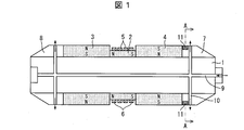
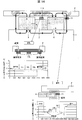
- FIG. 1 is a schematic cross-sectional view of the inspection probe 100.
- FIG. 2 is a cross-sectional view taken along the line AA shown in FIG.
- the inspection probe 100 is inserted into the tube of the magnetic material tube and moved in the tube, so that a magnetic vortex flaw detection method (magnetization ECT (Eddy-Current Testing)) and a magnetic flux resistance method (MFR; Magnetic) are performed. Flux Resistance).
- a magnetic vortex flaw detection method magnetization ECT (Eddy-Current Testing)
- MFR magnetic flux resistance method
- Flux Resistance Magnetic
- a pipe made of a magnetic material such as carbon steel, ferritic stainless steel, duplex stainless steel composed of two phases of a ferrite phase and an austenite phase can be used.
- the inspection probe 100 includes a yoke 1, a first magnet 2, a second magnet 3, a third magnet 4, an excitation / detection coil 5, an eddy current control coil 6, guides 7 and 8, air introduction holes. 9, an air injection hole 10, and a Hall element 11 are provided.
- the yoke 1 is a hollow cylindrical member made of a magnetic material.
- a high magnetic permeability metal such as carbon steel or low alloy steel can be used.
- the first magnet 2, the second magnet 3, and the third magnet 4 are attached to the outer peripheral surface of the yoke 1, and are arranged in this order so as to form a Halbach array along the axial direction of the yoke 1.
- the first magnet 2 is formed in a hollow cylindrical shape made of a single magnet or a hollow cylindrical shape in which a plurality of magnets divided in the circumferential direction are combined, and the axial center portion ( It is mounted along the outer peripheral surface of a position between the second magnet 3 and the third magnet 4.
- the first magnet 2 is formed in a hollow cylindrical shape, and is attached to the yoke 1 so that the axis thereof is collinear with the axis of the yoke 1.
- the first magnet 2 is polarized along a direction substantially parallel to the axial direction of the yoke 1 so that the magnetic pole on the second magnet 3 side is an N pole and the magnetic pole on the third magnet 4 side is an S pole. Is magnetized.
- a high-performance permanent magnet such as a neodymium magnet is used.
- the second magnet 3 is attached to the first magnet 2 in the yoke 1 along the outer peripheral surface on one end side in the axial direction.
- the second magnet 3 is formed in a hollow cylindrical shape composed of a single magnet or a hollow cylindrical shape combining a plurality of magnets divided in the circumferential direction, and the axis thereof is the axis of the yoke 1.
- the yoke 1 is mounted so as to be on the same straight line.
- the second magnet 3 is polarized along the radial direction of the yoke 1 (the direction facing the magnetic tube P), the magnetic pole on the yoke 1 side is the S pole, and the opposite side (the magnetic tube to be inspected). Side) magnetic poles are N poles.
- a high performance permanent magnet such as a neodymium magnet is used.
- the third magnet 4 is mounted along the outer peripheral surface of the other end side in the axial direction with respect to the first magnet 2 in the yoke 1 (opposite side to the side on which the second magnet 3 is disposed).
- the third magnet 4 is formed in a hollow cylindrical shape made of a single magnet or a hollow cylindrical shape in which a plurality of magnets divided in the circumferential direction are combined, and its axis is the axis of the yoke 1.
- the yoke 1 is mounted so as to be on the same straight line.
- the third magnet 4 is polarized along the radial direction of the yoke 1 (the direction facing the magnetic pipe P), and is magnetized so that the magnetic pole direction is opposite to that of the second magnet 3. .
- the third magnet 4 is magnetized so that the magnetic pole on the yoke 1 side is an N pole and the opposite magnetic pole is an S pole.
- the third magnet 4 for example, a high-performance permanent magnet such as a neodymium magnet is used.
- the first magnet 2 is mounted between the second magnet 3 and the third magnet 4 so that the magnetic pole on the second magnet 3 side is an N pole and the magnetic pole on the third magnet 4 side is an S pole. (That is, by arranging the second magnet 3, the first magnet 2, and the third magnet 4 so as to form a Halbach array), the strength of the magnetic flux formed by the second magnet 3 and the third magnet 4 (Magnetic flux density) can be increased and the magnetic flux distribution can be made uniform.
- the size of the first magnet 2, the second magnet 3, and the third magnet 4 is not particularly limited as long as it can be inserted into the magnetic pipe to be inspected, but the second magnet 3 and the third magnet are not limited. It is preferable that the magnetic flux density at the end portion on the outer side in the axial direction of the yoke 1 of 4 (end portion far from the first magnet 2) is in the range of 1.4T to 2.4T, More preferably within the range of 2.2T.
- the magnetic flux density is within the above range, the relative permeability of the magnetic pipe to be inspected with respect to the change of the magnetic flux density changes linearly. For this reason, by setting the magnetic flux density within the above range, inspection by a magnetic flux resistance method (MFR) described later can be performed with higher accuracy.
- MFR magnetic flux resistance method
- the number of magnets is not particularly limited.
- the number of magnets may be one or both of between the first magnet 2 and the second magnet 3 and between the first magnet 2 and the third magnet 4.
- another magnet may be provided. In that case, each magnet may be arranged so that each magnet forms a Halbach array.
- the method of attaching the first magnet 2, the second magnet 3, and the third magnet 4 to the yoke 1 is not particularly limited.
- the first magnet 2, the second magnet 3, and the third magnet 4 may be attached to the yoke 1 with an adhesive or the like. May be combined.
- the excitation / detection coil 5 is wound along the outer peripheral surface of the first magnet 2 disposed in the central portion of the yoke 1 in the axial direction, and the second magnet 3, the first magnet 2 in the magnetic pipe P, and This is for performing eddy current flaw inspection in which eddy current flaw detection is performed on a region magnetically saturated by the third magnet 4 (or a region where the magnetic permeability has decreased to such a level that eddy current can sufficiently penetrate).
- eddy current flaw inspection when the excitation / detection coil 5 passes through the thinned portion of the magnetic tube, it correlates with the amplitude according to the thinning amount (volume) and the phase according to the thinning depth.
- a thinning signal (detection signal) is detected.
- the configuration of the excitation / detection coil 5 is not particularly limited as long as the above thinning signal can be detected.
- a copper wire having a wire diameter of 0.02 to 1.0 mm and a number of turns of 10 to 200 is used.
- the coil can be used.
- the eddy current control coil 6 is wound around the excitation / detection coil 5 on the outer peripheral surface of the first magnet 2 at positions on both sides of the yoke 1 in the axial direction, and the eddy current is excited by the excitation / detection coil 5. Excites the eddy current flowing in the opposite direction.
- the excess conduction range of the eddy current excited by the excitation / detection coil 5 is canceled by exciting the eddy current in the reverse direction with the excitation coil, and the excess conduction of the eddy current. The range can be suppressed.
- illustration is abbreviate
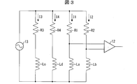
- FIG. 3 is a circuit diagram of the eddy current flaw detection part in the inspection probe 100.
- two excitation / detection coils 5 La, Lb
- two eddy current control coils 6 Lc, Ld
- four variable resistors R1, R2, R3, R4 are provided.
- the output terminal of the eddy current flaw detector 12 is connected to an eddy current flaw detector 30 described later by a conducting wire.
- the eddy current inspection is performed as follows. That is, first, the impedances of the excitation / detection coil 5 and the eddy current control coil 6 at a predetermined test frequency (for example, 100 kHz) and a predetermined applied voltage (for example, 5 v) are measured, and the resistances of the variable resistors R1 and R2 are measured. Adjust the value to the measured resistance value. Further, the combined impedance of the excitation / detection coil 5 and the variable resistors R1 and R2 at this time is measured, and the resistance values of the variable resistors R3 and R4 connected to the eddy current control coil 6 are measured before and after the measured resistance values. Flaw detection is performed, and finally flaw detection is performed under conditions where detection sensitivity is good. The flaw detection speed by the inspection probe 100 is set, for example, in the range of about 2 to 50 mm / second, and is set in the range of about 2 to 10 mm / second when it is necessary to accurately detect a smaller thickness reduction.
- the Hall element 11 is placed at a position near the end portion of the third magnet 4 on the side far from the first magnet 2 at substantially equal intervals along the circumferential direction of the yoke 1.
- Each of these Hall elements 11 outputs a voltage value (output signal) corresponding to the magnetic flux density (flux intensity) passing through the third magnet 4 and the magnetic tube to the magnetic flux resistance flaw detector 40 described later. That is, the Hall element 11 is disposed on a magnetic circuit formed by the third magnet 4 and the magnetic tube P, detects the magnetic flux density flowing through the magnetic circuit, and outputs an output signal corresponding to the detection result to the magnetic flux resistance flaw detector 40. Output to.
- the magnetic flux resistance flaw detection unit 40 uses the output signal of each Hall element 11 to quantitatively evaluate the thinning by the magnetic flux resistance method described later. In FIG. 1, illustration of the conducting wire of the hall element 11 and its extraction hole is omitted.
- the installation position of the Hall element 11 may be a position where the magnetic flux density passing through the third magnet 4 and the magnetic tube P can be measured.
- the hall element 11 is positioned in the axial direction of the inspection probe 100 with respect to the third magnet 4. The position which opposes may be sufficient and the position which opposes the circumferential direction may be sufficient. Further, the installation position of the Hall element 11 may be a position in contact with the third magnet 4 or may be a position separated from the third magnet 4.
- the magnetic flux density passing through the third magnet 4 and the magnetic tube P is measured by the Hall element 11, but not limited thereto, the Hall element 11 is connected to the second magnet 3 and the magnetic tube P.
- the magnetic flux density passing through the second magnet 3 and the magnetic material tube P may be measured on the magnetic circuit formed by
- Hall elements 11 are arranged on the magnetic circuit formed by the second magnet 3 and the magnetic tube P and on the magnetic circuit formed by the third magnet 4 and the magnetic tube P, respectively.
- the magnetic flux density passing through the body tube P and the magnetic flux density passing through the second magnet 3 and the magnetic body tube P may be measured.
- Guides 7 and 8 are provided at both axial ends of the inspection probe 100.
- the guides 7 and 8 are made of, for example, acetal resin or stainless steel, and are attached to the yoke 1 by a screw structure.
- air introduction holes 9 are provided at substantially central portions of the yoke 1 on both end surfaces in the axial direction of the yoke 1, and communicate with the air introduction holes 9 in the vicinity of both end portions of the yoke 1.
- a plurality of air injection holes 10 extending in the direction are provided. Thereby, air is introduced from the air introduction holes 9 provided on both end faces of the yoke 1, and air is ejected from the air ejection holes 10.
- the air injection hole 10 has a hole diameter of about 2 mm ⁇ and is provided with about 6 to 10 holes from the air introduction hole 9 in the circumferential direction.
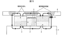
- FIG. 16 is an explanatory diagram showing a difference between a leakage flux method (MFL) that has been conventionally performed and a magnetic flux resistance method (MFR) used in the present embodiment.
- MFL leakage flux method
- MFR magnetic flux resistance method
- the leakage magnetic flux method As shown in FIG. 16, among the second magnet 3, the first magnet 2, and the third magnet 4 arranged in the Halbach array, the magnetic material tube in the first magnet 2 arranged in the center.
- a Hall element 11b is arranged on the surface facing P, and the Hall element 11b detects that the magnetic flux flowing in the magnetic pipe P leaks outside the pipe at the thinned portion of the magnetic pipe P.
- the leakage magnetic flux is generated only in the shape discontinuity portion such as the thinning end portion, and as shown in FIG. 16, the leakage magnetic flux is not generated in the entire thinning portion or the gentle thinning portion. Therefore, the leakage magnetic flux method cannot detect the entire thinning or a gradual thinning portion, or quantitatively evaluate the thinning.
- the magnet (the third magnet 4 polarized in the direction facing the magnetic tube P) disposed at the end of the Halbach array and the magnetic circuit formed by the magnetic tube P are arranged on the magnetic circuit.
- the Hall element 11 is arranged, and the magnetic flux density flowing through the magnet and the magnetic tube P is measured.
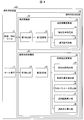
- FIG. 4 is a block diagram showing a configuration of the thinning measuring apparatus 200 according to the present embodiment.
- FIG. 5 is explanatory drawing which shows the outline
- the thinning measuring apparatus 200 includes an excitation / detection coil 5, a Hall element 11, and a thinning determination processing unit 20. Further, the thinning determination processing unit 20 includes an eddy current flaw detection unit 30 and a magnetic flux resistance flaw detection unit 40.
- the eddy current flaw detection inspection is performed by the excitation / detection coil 5, and the eddy current flaw detection portion 30 is formed on the inner surface of the magnetic pipe P using the detection signal of the eddy current flaw inspection.
- the magnetic flux density flowing through the third magnet 4 and the magnetic tube P is detected by the Hall element 11, and the magnetic resistance test unit 40 is magnetic by using the detection result and the determination result of the thinned surface by the eddy current testing unit 30.
- the thinning of the body tube P is quantitatively evaluated.
- the inner surface of the magnetic tube P is the surface that is the facing surface between the magnetic tube P and the inspection probe 100, and the outer surface is the back surface of the facing surface.
- the eddy current flaw detection unit 30 includes a first detection unit 31, a first storage unit 32, and an eddy current flaw detection calculation unit 33.
- a meat surface determination unit 35 is provided.
- the magnetic flux resistance flaw detection unit 40 includes a second detection unit 41, a second storage unit 42, and a magnetic flux resistance calculation unit 43.
- the magnetic flux resistance calculation unit 43 includes a detection position specifying unit 44 and a cross-sectional defect rate calculation unit 45. , A shape parameter calculation unit 46, a thinning range calculation unit 47, and a thinning depth calculation unit 48.
- the first detection unit 31 acquires a detection signal input from the excitation / detection coil 5 via the eddy current flaw detector 12, and associates the acquired detection signal with a detection time (detection timing) when the detection signal is detected. In addition, it is stored in the first storage unit 32.
- the second detection unit 41 acquires the output voltage value of each Hall element 11 and stores the acquired voltage value and the detection time (detection timing) of each voltage value in the second storage unit 42 in association with each other.
- the configurations of the first storage unit 32 and the second storage unit 42 are not particularly limited.
- a tape system such as a magnetic tape or a cassette tape
- a magnetic disk such as a floppy (registered trademark) disk / hard disk
- a CD-ROM Disc systems including optical disks such as / MO / MD / DVD / CD-R, card systems such as IC cards (including memory cards) / optical cards, mask ROM / EPROM / EEPROM (registered trademark) / flash ROM, etc.
- a recording medium such as a semiconductor memory system can be used.
- the detection position specifying unit 34 and the detection position specifying unit 44 include the detection signal and the detection time of the excitation / detection coil 5 stored in the first storage unit 32, and the Hall elements stored in the second storage unit 42.
- the detection position corresponding to the detection signal of the excitation / detection coil 5 in the magnetic tube P and the detection position corresponding to the voltage output value of each Hall element 11 are associated with each other based on the output voltage value of 11 and the detection time thereof.
- the thinning surface determination unit 35 determines whether the thinning present in the magnetic pipe to be inspected is the thinning of the inner surface or the outer surface based on the detection signal of the excitation / detection coil 5.
- the cross-sectional defect rate calculation unit 45 calculates the cross-sectional defect rate at each position along the axial direction of the magnetic tube based on a cross-sectional defect rate calculation formula described later.
- the cross-sectional defect rate is the ratio of the cross-sectional area missing to the cross-sectional area in the cross-section perpendicular to the axial direction of the magnetic tube, and the deficient cross-sectional area is the cross-sectional area reduced due to thinning.
- different cross-sectional defect rate calculation formulas are used for the case of inner surface thinning and the case of outer surface thinning.
- the shape parameter calculation unit 46 calculates a shape parameter based on the output voltage value of each Hall element 11.
- the shape parameter calculation unit 46 normalizes (divides) Vmax, which is the maximum value among the output voltage values of each Hall element 11, and the output voltage value of each Hall element 11 by Vmax as the shape parameters.
- Vall which is the sum of the values obtained, is calculated.
- the thinning range calculation unit 47 calculates the thinning range of the magnetic tube based on the output voltage value of each Hall element 11.
- the thinning depth calculation unit 48 is based on the cross-sectional defect rate calculated by the cross-sectional defect rate calculation unit 45 and the thinning range calculated by the thinning range calculation unit 47, and is thinned in the radial direction of the magnetic pipe. Depth is calculated.
- the eddy current flaw detection calculation unit 33 and the magnetic flux resistance calculation unit 43 may be an integrated circuit (hardware logic) such as ASIC (Application specific integrated circuit), and a computer equipped with a processor such as a CPU executes software. It may be realized by things, or may be realized by combining them.
- ASIC Application specific integrated circuit
- the eddy current flaw detection calculation unit 33 and the magnetic flux resistance calculation unit 43 are provided in a common housing with the first detection unit 31, the first storage unit 32, the second detection unit 41, and the second storage unit 42. It may be provided separately. In the latter case, the eddy current flaw detection calculation unit 33 and the magnetic flux resistance calculation unit 43 transfer the information stored in the first storage unit 32 and the second storage unit 42 via wired communication, wireless communication, or a removable storage medium. To obtain and perform arithmetic processing.
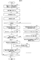
- FIG. 6 is a flowchart showing the flow of the thinning inspection process in the present embodiment.
- the inspection probe 100 is inserted into a magnetic tube to be inspected, and measurement processing is performed by the excitation / detection coil 5 and the Hall element 11 while moving in the magnetic tube along the axial direction (S1).
- the first detection unit 31 acquires a detection signal output from the excitation / detection coil 5 via the eddy current flaw detector 12 and a detection time when the detection signal is detected, and associates them with the first detection signal.
- the data is stored in the storage unit 32.
- the second detection unit 41 acquires the output voltage value of each Hall element 11 and the detection time when the voltage value is detected, and stores them in the second storage unit 42 in association with each other.
- the method for moving the inspection probe 100 in the magnetic tube is not particularly limited.
- the inspection probe 100 may be moved by pulling a wire or the like connected to the inspection probe 100, and the inspection probe 100 is pushed by a rod-shaped member.
- the inspection probe 100 may be provided with a driving means to be self-propelled.
- the detection position specifying units 34 and 44 detect the position corresponding to the detection signal of the excitation / detection coil 5 (the axial position of the magnetic tube). Is associated with a detection position (position in the axial direction of the magnetic tube) corresponding to the output voltage value of the Hall element 11 (S2).
- the thinning surface determination unit 35 extracts one of the detection positions associated in S2 as the attention detection position (S3), and the thinning surface determination process of the detection position (thinning of the inspection position) Is performed (S4).
- the evaluation of the thinning of the outer surface (S5 to S11) is used to quantitatively evaluate the thinning (calculation of cross-sectional defect rate, thinning range, and thinning depth).
- a quantitative evaluation of the thinning is performed by the evaluation algorithm (S12 to S15) for inner surface thinning.
- the phase angle of the output voltage value is clearly different between the case where the thinning is present on the inner surface side and the outer surface side of the magnetic tube.
- the detection result is the first quadrant. If the thinning is present on the outer surface, it swings to the third quadrant side. Therefore, by using the magnetized eddy current flaw detection method, it can be easily determined whether the thinning is present on the inner surface side or the outer surface side of the magnetic tube.
- the thinning surface (whether thinning is present on the outer surface side of the magnetic tube or on the inner surface side) is determined by the magnetized eddy current flaw detection method.
- the measurement data acquisition by the magnetic flux resistance method and the measurement data acquisition by the magnetic eddy current flaw detection method can be simultaneously performed, and the thinning surface determination can be performed in real time.
- the thinning surface determination by the magnetized eddy current flaw detection method is particularly advantageous.
- the method for determining the thinned surface is not limited to the magnetized eddy current flaw detection method, and may be determined using another determination method.
- the thinning surface may be determined by the user.
- the cross-sectional defect rate calculation unit 45 determines whether or not the thinning of the target inspection position is the thinning of the outer surface based on the thinning surface determination result by the thinning surface determination unit 35 (S5).
- the cross-sectional defect rate calculation unit 45 calculates a cross-sectional defect rate Cout based on the cross-sectional defect rate calculation formula for outer surface thinning (S6).
- cross-sectional defect ratio calculation formula for the outer surface thinning and the cross-section defect ratio calculation formula for the inner surface thinning are based on a test piece (magnetic test tube) having a plurality of types of thinning using a test probe 100 and a magnetic flux. It sets beforehand based on the result measured by the resistance method.
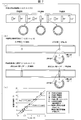
- FIG. 7 is explanatory drawing which shows an example of the test piece which has several outer surface thinning
- (b) is explanatory drawing which shows an example of the test piece which has several inner surface thinning.
- the outer surface thinning test piece is an STB tube having an outer diameter of 25.4 mm and a wall thickness of 2.0 mm.
- a test piece on which meat was formed was used. That is, the [thinning range and thinning ratio] are [45 °, 25%], [45 °, 50%], [45 °, 75%], [90 °, 25%], [90 °, 50 %], [90 °, 75%], [135 °, 25%], [135 °, 50%], and [135 °, 75%] test pieces having 9 types of thinning were used.
- the thinning range in the circumferential direction is 360 degrees, it indicates that thinning has occurred over the entire circumference of the magnetic pipe P.
- the thinning ratio in the present embodiment indicates the ratio of the depth of the thinned portion in the direction in which the magnetic pipe P and the first magnet 2 face each other with respect to the thickness of the magnetic pipe P in a healthy state. It is a value and if the thickness reduction rate is 75%, it indicates that the thickness of the magnetic pipe P is 1 ⁇ 4 of the healthy state.
- the axial width of the magnetic tube in each thinning is 5 mm.
- an STB tube having an outer diameter of 25.4 mm and a wall thickness of 2.0 mm is provided with a diameter of 5 mm and a thickness reduction rate of 25%.
- an STB tube with an outer diameter of 25.4 mm and a wall thickness of 2.0 mm Thickness range 90 °, thinning rate 25%, thinning of magnetic tube axial width 5mm, and thinning range 90 °, thinning rate 50%, thinning of magnetic tube axial width 5mm The formed test piece was used.
- FIG. 5 is a graph showing a relationship between an actual cross-sectional defect rate (cross-sectional defect rate calculated based on an actual measurement value) of each thinning in each test piece.
- the actual measurement value was measured using an ultrasonic thickness meter or a water immersion rotary ultrasonic thickness measurement method.
- the graph also plots the results of measuring the outer circumferential groove thinning (outer circumferential groove thinning) and the inner circumferential groove thinning (inner circumferential groove thinning).
- a cross-sectional defect rate calculation formula for calculating the cross-sectional defect rate from V_sum is calculated in advance based on the relationship between V_sum based on the measurement result of the test specimen prepared in advance and the actual cross-sectional defect rate. Keep it.
- the shape parameter calculation unit 46 calculates a predetermined shape parameter based on the output voltage value of each Hall element 11 (S7).
- Vmax which is the maximum value among the output voltage values of each Hall element 11 and Val which is a total value of values obtained by normalizing the output voltage values of each Hall element 11 by Vmax are used as shape parameters. calculate.
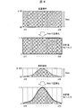
- FIG. 8 is an explanatory diagram showing an example of output voltage values of the eight Hall elements 11 (ch1 to ch8) when full-thickness thinning and local thinning are detected.
- the output voltage value has a rectangular distribution when the entire surface is thinned so that the output voltage values of all the Hall elements 11 are substantially the same.
- the output voltage value of the Hall element 11 arranged immediately below the local thinning portion is the highest, and the output voltage value decreases as the distance from the Hall element 11 increases.
- the thinning range calculation unit 47 determines whether or not the thinning range can be calculated by the predetermined first calculation method using the shape parameters (Vmax, Val) calculated by the shape parameter calculation unit 46. (S8). The determination method in S8 will be described later.
- the thinning range calculation unit 47 calculates the thinning range by the first calculation method (S9), and by the first calculation method, If it is determined that the thinning range cannot be calculated, the thinning range calculation unit 47 calculates the thinning range by a predetermined second calculation method (S10).
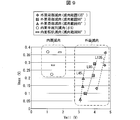
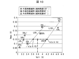
- FIG. 9 shows the calculation of Vmax and Vall based on the results of flaw detection of the above-described thinning test piece (see FIG. 7A) and internal thinning test piece (see FIG. 7B).
- the graph is plotted with the horizontal axis as Vall and the vertical axis as Vmax.
- FIG. 10 is a graph obtained by extracting data related to the test piece for external thinning from the data shown in FIG.
- a straight line L90 indicating the correlation between Vall and Vmax and a straight line L135 indicating the correlation between Vall and Vmax when the thickness reduction range is 135 ° are calculated in advance.
- the intersection between Vmax obtained by flaw detection of the magnetic tube to be inspected and each of the straight lines L45, L90, and L135 is calculated, and the Val obtained by flawing the magnetic tube to be inspected and each of the above intersections are calculated.
- the thickness reduction range is calculated according to the ratio of the calculated differences.
- the Val value is an evaluation map (FIG. 10). ), And the thickness reduction range cannot be calculated by the first calculation method.
- the thinning range calculation unit 47 is (i) external thinning and the value of the Val is less than a predetermined value (for example, 3), and (ii) internal thinning,
- the thickness reduction range is calculated using a second calculation method described below. That is, in the case of external thinning, the thinning range calculation unit 47 determines whether or not the value of Vall is greater than or equal to a predetermined value in the process of S8. The thickness reduction range is calculated, and if it is less than the predetermined value, the thickness reduction range is calculated by the second calculation method in S10. Further, in the case of internal thinning, the thinning range calculation unit 47 calculates the thinning range by using the second calculation method in the process of S14 described later.
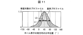
- FIG. 11 is an explanatory diagram showing a method for calculating a thinning range by the second calculation method.
- the standard thinning when measuring the thinning of the outer surface is the thinning range of 45 °, and the thinning with a thinning rate of 25% is the standard thinning.
- the thinning (arc-shaped thinning) with a thinning range of 90 ° and a thinning rate of 50% is set as the standard thinning. It should be noted that which thinning in the test piece is used as the reference thinning may be selected as appropriate in accordance with a verification experiment conducted in advance.
- the reference profile which is a shape profile of reference thinning (a profile obtained by connecting the output voltages of the hall elements 11 normalized by Vmax), both sides of the hall element 11 in which Vmax is detected.
- the distance L1 between the two points corresponding to the reference value in the reference profile is calculated using the average value of the output voltage values of the Hall elements 11 arranged at the reference value as the reference value.
- the distance L2 between the two points corresponding to the reference value in the shape profile obtained based on the result of the flaw detection of the magnetic pipe to be detected is calculated.
- Vmax 1 and Vmax are detected.
- a virtual profile is obtained by connecting the output voltages of the Hall elements 11 on both sides of the Hall element 11 normalized by Vmax with straight lines or curves, and the distance between the two points corresponding to the reference value in the virtual profile is expressed as a distance. What is necessary is just to calculate as L2.
- the thinning depth calculation unit 48 calculates the thinning depth based on the thinning loss rate and the thinning range (S11).
- the thinning depth d in the case of thinning of the outer surface is the radius of the outer diameter of the magnetic pipe to be inspected r (mm), the thickness of the healthy part t (mm), and the thinning loss rate S ( %)
- the cross-sectional defect rate calculation unit 45 calculates the cross-sectional defect rate Cin based on the above-described cross-sectional defect rate calculation formula for inner surface thinning. (S12).
- the shape parameter calculation unit 46 calculates a shape parameter based on the output voltage value of each Hall element 11 (S13).
- Vmax and Vall are calculated as shape parameters, as in the case of thinning of the outer surface.
- the thinning range calculation unit 47 calculates the thinning range by the second calculation method (S14).
- the thinning (arc-shaped thinning) with a thinning range of 90 ° and a thinning ratio of 50% is set as the standard thinning.
- the thickness reduction range is calculated by the second calculation method using the shape profile as a reference profile.
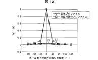
- FIG. 12 is an explanatory diagram illustrating a method for calculating a thinning range by the second calculation method.
- the thinning depth calculation unit 48 calculates the thinning depth based on the thinning loss rate and the thinning range (S15), and the process ends.
- the thinning depth d is the radius of the outer diameter of the magnetic pipe to be inspected r (mm), the thickness of the healthy part t (mm), and the thickness loss rate S ( %)
- the thinning surface determination unit 35 determines whether or not the calculation processing of the cross-sectional defect rate, the thinning range, and the thinning depth has been completed for all the inspection positions (S16), and the calculation processing is not performed. If the detected position remains, the process returns to S3 and the same processing is repeated. If it is determined in S16 that the calculation process has been completed for all the detected positions, the thinning inspection process is terminated.
- FIG. 13 shows the relationship between the wall thickness evaluation value obtained by measuring the pipe used in the actual machine by the method of the present embodiment and the wall thickness actual measurement value obtained by actually measuring the pipe used in the actual machine. It is a graph.
- the wall thickness evaluation value is calculated by calculating the thinning depth of the pipe used in the actual machine by the method of the present embodiment, and calculating the difference between the thin wall thickness and the thinning depth in a healthy state, The actual measured thickness was measured using an ultrasonic thickness meter or a water immersion rotary ultrasonic thickness measurement method. As shown in this figure, the thickness evaluation can be performed with an accuracy of approximately ⁇ 0.15 mm by the method according to the present embodiment.
- FIG. 14A is a graph plotting the output voltage of each Hall element 11 when an STB tube (magnetic tube) having an outer diameter of 27.2 mm and a wall thickness of 2.6 mm in which the inner wall thickness is reduced is inspected. It is.
- FIG. 15A is a graph plotting the output voltage of each Hall element 11 when inspecting an STB tube (magnetic tube) having an outer diameter of 25.4 mm and a wall thickness of 2.0 mm in which the outer surface is thinned. It is.
- the corrosion (thinning) was caused by local thinning over a substantially entire area in the tube axis direction and local thinning at the baffle.
- the inspection probe 100 is arranged on the magnetic circuit formed by the third magnet 4 and the third magnet 4 and the magnetic tube, and detects the magnetic flux density flowing through the magnetic circuit.
- a Hall element 11 is provided, and the thinning of the magnetic tube is quantitatively evaluated based on the output signal of the Hall element 11 when the inspection probe 100 is moved along the axial direction in the magnetic tube.
- the inner surface thinning evaluation algorithm or the outer surface thinning evaluation Apply algorithm to quantitatively evaluate thinning.
- the configuration in which the inspection probe 100 includes the yoke 1 is shown, but the yoke 1 is not necessarily provided. In other words, the inspection probe 100 only needs to have a configuration that can apply the magnetic flux density shown in FIG.
- the 2nd magnet 3 and the 3rd magnet 4 are arrange
- inspection probe 100 may become a direction facing the magnetic body pipe P.
- the present invention is not limited to this, and any configuration can be used as long as the magnetic flux density shown in FIG.
- the second magnet 3 and the third magnet 4 may be arranged such that the axial direction of the magnetic pipe P and the polarization direction are parallel to each other. Even in such a case, the Hall element 11 and the yoke 1 may be provided on the magnetic circuit constituted by the second magnet 3 and the third magnet 4 and the magnetic material tube P.
- the inspection probe 100 is inserted into the magnetic pipe P to be inspected, and the measurement process using the Hall element 11 is performed while moving in the magnetic pipe P along the axial direction. It is not limited to. That is, by inserting the inspection probe 100 into the magnetic pipe P to be inspected and measuring the output of the Hall element 11 at an arbitrary position in the magnetic pipe P, quantitative evaluation of defects at the position of the magnetic pipe P is performed. It is good also as composition which performs.
- a defect measurement method is a defect measurement method for a magnetic member, and is arranged on a magnetic circuit formed by a magnet and the magnet and the magnetic member, and the magnetic flux density flowing through the magnetic circuit
- the determination result of the defect surface determination step Applying an evaluation algorithm according to the output signal of the magnetic sensor to perform a quantitative evaluation of defects of the magnetic member. It is characterized.
- the magnetic sensor using the inspection probe comprising a magnet and a magnetic sensor that is disposed on a magnetic circuit formed by the magnet and the magnetic member and detects a magnetic flux density flowing through the magnetic circuit.
- Quantitative evaluation of defects using the magnetic flux resistance method is performed quickly and appropriately by measuring the output of the magnetic sensor and applying an evaluation algorithm according to the determination result of the defect surface determination process to the output signal of the magnetic sensor Can do.
- the method includes an eddy current flaw detection process for performing an eddy current flaw inspection of the magnetic member, and in the defect surface determination step, whether the defect exists on the front or back surface of the magnetic member based on a result of the eddy current flaw inspection. You may make it determine.
- the quantitative evaluation of the defect is quickly and appropriately performed using the magnetic flux resistance method. Can be done.
- the inspection probe is disposed at a central portion of the Halbach array of the plurality of magnets and a plurality of magnets disposed so as to form a Halbach array along a surface facing the magnetic member.
- An eddy current flaw detection sensor for performing the eddy current flaw inspection disposed on a surface of the magnet facing the magnetic member, wherein the magnetic sensor is an end of the Halbach array of the plurality of magnets. It may be arranged on a magnetic circuit formed by the magnet and the magnetic body member, and detect the magnetic flux density flowing through the magnetic circuit.
- the magnetic member may be a magnetic tube, and in the measurement step, the inspection probe may be moved along the axial direction of the magnetic tube within the magnetic tube.
- the quantitative evaluation of the defect in the magnetic tube can be performed quickly and appropriately.
- the magnetic sensor outputs a voltage value corresponding to the magnetic flux density
- the evaluation step calculates a cross-sectional defect rate that is a ratio of a cross-sectional area that is deficient with respect to a cross-sectional area in a cross-section perpendicular to the axial direction of the magnetic tube.
- the cross-sectional defect rate of the defect in the magnetic tube can be calculated quickly and appropriately.
- the evaluation step includes a defect range calculation step of calculating a defect range indicating a defect range along a circumferential direction in a cross section perpendicular to the axial direction of the magnetic tube, and the defect range calculation step
- the defect range of the defect in the magnetic tube may be calculated based on the maximum value of the voltage value and the total value obtained by dividing the output voltage value of each magnetic sensor by the maximum value.
- the defect range of the defect of the magnetic tube can be calculated quickly and appropriately.
- the evaluation step includes a defect range calculating step for calculating a defect range indicating a defect range along a circumferential direction in a cross section perpendicular to the axial direction of the magnetic tube, and a defect occurring in the magnetic tube.
- a defect depth calculation step for calculating a defect depth, and in the defect range calculation step, among the output voltage values of the respective magnetic sensors when a plurality of types of defects formed in the test magnetic tube are measured , A total value of values obtained by dividing the output voltage value of each magnetic sensor by the maximum value, and a relationship with an actual defect range of each defect formed in the test magnetic tube.
- the radius of the outer diameter of the magnetic tube is r (mm)
- the cross-sectional defect rate calculated in the cross-sectional defect rate calculating step is S (%)
- the defect range calculated in the defect range calculation step is ⁇ (°) and the defect depth is d (mm)
- the defect depth of the defect in the magnetic tube can be calculated quickly and appropriately.
- a defect measuring apparatus is a defect measuring apparatus for a magnetic member, and is arranged on a magnet and a magnetic circuit formed by the magnet and the magnetic member, and the magnetic flux density flowing through the magnetic circuit
- An inspection probe including a magnetic sensor for detecting the magnetic sensor, and a magnetic flux resistance calculation unit capable of quantitatively evaluating defects of the magnetic member based on an output signal of the magnetic sensor, Applying an evaluation algorithm to the output signal, which is selected depending on whether a defect is formed on the surface of the magnetic member facing the inspection probe or on the back surface of the facing surface. It is the structure which can perform the quantitative evaluation of the defect of a magnetic body member.
- said structure using said test
- the said magnetic sensor By applying an evaluation algorithm that is selected according to whether the defect is formed on the front or back surface of the magnetic member to the output signal, the quantitative evaluation of the defect can be performed quickly and appropriately using the magnetic flux resistance method. Can be done.
- the inspection probe is disposed at a central portion of the Halbach array of the plurality of magnets and a plurality of magnets disposed so as to form a Halbach array along a surface facing the magnetic member.
- a defect surface determination unit that can determine whether a defect exists on the front or back surface of the magnetic member based on a result of the eddy current flaw inspection using the eddy current flaw detection sensor. And applying an evaluation algorithm selected according to a determination result of the defect surface determination unit to the output signal, to quantitatively evaluate the defect of the magnetic member. It may be configured to kill.
- the working efficiency can be improved.
- the magnetic member is a magnetic tube
- the magnetic flux resistance calculation unit outputs an output signal of each magnetic sensor when the inspection probe is moved in the magnetic tube along the axial direction of the magnetic tube. It is good also as a structure which can perform the quantitative evaluation of the defect of the said magnetic body pipe
- the quantitative evaluation of defects in the magnetic tube can be performed quickly and appropriately.
- the magnetic sensor outputs a voltage value corresponding to a magnetic flux density
- the magnetic flux resistance calculation unit is a cross-sectional defect that is a ratio of a cross-sectional area missing to a cross-sectional area in a cross-section perpendicular to the axial direction of the magnetic tube.
- the cross-sectional defect rate calculation formula set in advance based on the relationship between the total value of the output voltage values of each and the actual cross-sectional defect rate of each of the defects formed in the test magnetic tube, and the magnetic tube is measured It is good also as a structure which can calculate the cross-sectional defect
- the cross-sectional defect rate of the defect in the magnetic tube can be calculated quickly and appropriately.
- the magnetic flux resistance calculation unit includes a defect range calculation unit capable of calculating a defect range indicating a defect range along a circumferential direction in a cross section perpendicular to the axial direction of the magnetic tube, and the defect range calculation.
- the unit divides the maximum value among the output voltage values of each magnetic sensor when measuring a plurality of types of defects formed in the test magnetic tube, and the output voltage value of each magnetic sensor by the maximum value.
- the total value of the values, the defect range calculation data set in advance based on the relationship between the actual defect ranges of the respective defects formed in the test magnetic tube, and the respective magnets when the magnetic tube is measured The defect range of the magnetic tube may be calculated based on the maximum value of the output voltage value of the sensor and the total value obtained by dividing the output voltage value of each magnetic sensor by the maximum value. .
- the defect range of the defect in the magnetic tube can be calculated quickly and appropriately.
- the magnetic flux resistance calculation unit includes a defect range calculation unit capable of calculating a defect range indicating a defect range along a circumferential direction in a cross section perpendicular to the axial direction of the magnetic tube, and the magnetic tube.
- a defect depth calculation unit that calculates a defect depth of a defect that has occurred, and the defect range calculation unit outputs each of the magnetic sensors when measuring a plurality of types of defects formed in the test magnetic tube. Based on the relationship among the maximum value of the voltage values, the total value obtained by dividing the output voltage value of each magnetic sensor by the maximum value, and the actual defect range of each defect formed in the magnetic test tube.
- the defect depth may be calculated.
- the defect depth of the defect in the magnetic tube can be calculated quickly and appropriately.
- An inspection probe is an inspection probe for inspecting a defect of a magnetic member, and includes a plurality of Halbach arrays arranged along a surface facing the magnetic member.
- a magnet a sensor for eddy current flaws disposed at a central portion of the Halbach array of the plurality of magnets, a magnet disposed at an end of the Halbach array of the plurality of magnets, and the magnetic member.
- the magnetic sensor is arranged on a magnetic circuit to be formed, and includes a magnetic sensor that detects a magnetic flux density flowing through the magnetic circuit.
- the defect can be quantitatively evaluated by the magnetic flux resistance method.
- the measurement data acquisition by the eddy current flaw detection sensor and the measurement data acquisition by the magnetic sensor can be performed in parallel, the working efficiency can be improved.
- a cylindrical yoke made of a magnetic material is provided, and the magnets are arranged side by side in a Halbach array along the axial direction of the yoke, and each of the magnets is cylindrical along the outer peripheral surface of the yoke
- the magnetic sensors may be arranged in a plurality along the circumferential direction of the yoke.
- the quantitative evaluation of defects in the magnetic tube can be performed quickly and appropriately.
- the present invention can be applied to a defect measuring method and a defect measuring apparatus for measuring a defect of a member made of a magnetic material, and an inspection probe used for measuring the defect.
Abstract
Description
図1は、検査プローブ100の断面模式図である。また、図2は図1に示したA-A断面の断面図である。 (1-1. Configuration of Inspection Probe 100)
FIG. 1 is a schematic cross-sectional view of the
図16は、従来から行われている漏洩磁束法(MFL;Magnetic Flux Leakage)と本実施形態で用いる磁束抵抗法(MFR;Magnetic Flux Resistance)との違いを示す説明図である。 (1-2. Outline of magnetic flux resistance method)
FIG. 16 is an explanatory diagram showing a difference between a leakage flux method (MFL) that has been conventionally performed and a magnetic flux resistance method (MFR) used in the present embodiment.
図4は、本実施形態にかかる減肉測定装置200の構成を示すブロック図である。また、図5は、本実施形態における減肉判定処理の概要を示す説明図である。 (1-3. Configuration of the thinning determination processing unit 20)
FIG. 4 is a block diagram showing a configuration of the thinning measuring
図6は、本実施形態における減肉検査処理の流れを示すフローチャートである。 (1-4. Thinning inspection process)
FIG. 6 is a flowchart showing the flow of the thinning inspection process in the present embodiment.
d=r-{r2-S・360/(π・θ)}1/2
より算出することができる。 In addition, the thinning depth d in the case of thinning of the outer surface is the radius of the outer diameter of the magnetic pipe to be inspected r (mm), the thickness of the healthy part t (mm), and the thinning loss rate S ( %) And the thinning range is θ (°)
d = r− {r 2 −S · 360 / (π · θ)} 1/2
Can be calculated.
d={(r-t)2+S・360/(π・θ)}1/2-(r-t)
より算出することができる。 In addition, in the case of inner wall thinning, the thinning depth d is the radius of the outer diameter of the magnetic pipe to be inspected r (mm), the thickness of the healthy part t (mm), and the thickness loss rate S ( %) And the thinning range is θ (°)
d = {(rt) 2 + S · 360 / (π · θ)} 1 / 2- (rt)
Can be calculated.
(1-5-1.内面減肉の評価例)
図14の(a)は、内面減肉が生じている外径27.2mm、肉厚2.6mmのSTB管(磁性体管)を検査したときの各ホール素子11の出力電圧をプロットしたグラフである。 (1-5. Evaluation example of thinning inspection)
(1-5-1. Evaluation example of inner wall thinning)
FIG. 14A is a graph plotting the output voltage of each
<代表的な減肉部の評価結果>
(1)減肉面判定結果:内面減肉
(2)各ホール素子11の出力電圧の合計値V_sum=1.19V
(3)断面欠損率S=16.7%(35.9mm2)(a=16.163、b=2.5)(4)周方向の減肉範囲θ=110°
(内面減肉であることから第2算出方法により減肉範囲θを算出した。すなわち、図14の(b)に示すようにL1,L2を求め、L2/L1=1.96を算出した。そして、L2/L1を基準減肉の減肉範囲(56.3°)に乗算することにより、上記評価例の減肉範囲θ=56.3×1.96≒110°を算出した。)
(5)減肉深さd=1.6mm
(内面減肉であることから、d={(r-t)2+S・360/(π・θ)}1/2-(r-t)より減肉深さdを算出した。)
(1-5-2.外面減肉の評価例)
図15の(a)は、外面減肉が生じている外径25.4mm、肉厚2.0mmのSTB管(磁性体管)を検査したときの各ホール素子11の出力電圧をプロットしたグラフである。 About this evaluation example, when the representative thinning part shown to (a) of FIG. 14 was evaluated according to the flow shown in FIG. 6, the following results were obtained.
<Evaluation results of typical thinning parts>
(1) Thinning surface determination result: Inner surface thinning (2) Total value of output voltage of each
(3) Cross-sectional defect rate S = 16.7% (35.9 mm 2 ) (a = 16.163, b = 2.5) (4) Thinning range in the circumferential direction θ = 110 °
(Because it is inner surface thinning, the thinning range θ was calculated by the second calculation method. That is, L1 and L2 were obtained as shown in FIG. 14B, and L2 / L1 = 1.96 was calculated. Then, by multiplying L2 / L1 by the thinning range (56.3 °) of the standard thinning, the thinning range θ = 56.3 × 1.96≈110 ° of the evaluation example was calculated.)
(5) Thinning depth d = 1.6mm
(Because of the thinning of the inner surface, the thinning depth d was calculated from d = {(rt) 2 + S · 360 / (π · θ)} 1 / 2- (rt).)
(1-5-2. Evaluation example of outer wall thinning)
FIG. 15A is a graph plotting the output voltage of each
<代表的な減肉部の評価結果>
(1)減肉面判定結果:外面減肉
(2)各ホール素子11の出力電圧の合計値V_sum=0.27V
(3)断面欠損率S=4.4%(6.5mm2)(a=16.163)
(4)減肉範囲θ=51.3°
(外面減肉であるが、Vall<3.0Vなので第2算出方法により減肉範囲θを算出した。すなわち、図15の(b)に示すようにL1,L2を求め、L2/L1=1.14を算出した。そして、L2/L1を基準減肉の減肉範囲(45.0°)に乗算することにより、上記評価例の減肉範囲θ=45.0×1.14≒51.3°を算出した。)
(5)減肉深さd=0.69mm
(外面減肉であることから、d=r-{r2-S・360/(π・θ)}1/2より減肉深さdを算出した。)
(1-6.まとめ)
以上のように、本実施形態では、検査プローブ100は、第3磁石4と、第3磁石4と磁性体管とが形成する磁気回路上に配置され、当該磁気回路を流れる磁束密度を検知するホール素子11とを備えており、この検査プローブ100を磁性体管内で軸方向に沿って移動させたときのホール素子11の出力信号に基づいて磁性体管の減肉の定量的評価を行う。この際、減肉が磁性体管の内面側に生じているか裏面側に生じているか(内面減肉か外面減肉か)に応じて、内面減肉用の評価アルゴリズムまたは外面減肉用の評価アルゴリズムを適用して減肉の定量的評価を行う。 About this evaluation example, when the typical thinning part was evaluated according to the flow shown in FIG. 6, the following results were obtained.
<Evaluation results of typical thinning parts>
(1) Thinning surface determination result: Outer surface thinning (2) Total value of output voltage of each
(3) Cross-sectional defect rate S = 4.4% (6.5 mm 2 ) (a = 16.163)
(4) Thinning range θ = 51.3 °
(Although it is thinning on the outer surface, Vall <3.0V, the thinning range θ is calculated by the second calculation method. That is, L1 and L2 are obtained as shown in FIG. 15B, and L2 / L1 = 1. 14 was calculated by multiplying L2 / L1 by the thinning range of the standard thinning (45.0 °) to obtain the thinning range θ = 45.0 × 1.14≈51. 3 ° was calculated.)
(5) Thinning depth d = 0.69mm
(Because of the thinning of the outer surface, the thinning depth d was calculated from d = r− {r 2 −S · 360 / (π · θ)} 1/2 .)
(1-6. Summary)
As described above, in the present embodiment, the
本発明の一態様にかかる欠陥測定方法は、磁性体部材の欠陥測定方法であって、磁石と、前記磁石および前記磁性体部材が形成する磁気回路上に配置され、当該磁気回路を流れる磁束密度を検知する磁気センサとを備える検査プローブを用い、前記磁気センサの出力を測定する測定工程と、欠陥が前記磁性体部材における前記検査プローブとの対向面である表面に生じている表面欠陥であるのか、当該対向面の裏面に生じている裏面欠陥であるのかを判定する欠陥面判定工程と、表面欠陥および裏面欠陥のそれぞれについて予め設定された評価アルゴリズムのうち、前記欠陥面判定工程の判定結果に応じた評価アルゴリズムを前記磁気センサの出力信号に適用することにより、前記磁性体部材の欠陥の定量的評価を行う評価工程とを含むことを特徴としている。 (Other)
A defect measurement method according to an aspect of the present invention is a defect measurement method for a magnetic member, and is arranged on a magnetic circuit formed by a magnet and the magnet and the magnetic member, and the magnetic flux density flowing through the magnetic circuit A measurement step of measuring an output of the magnetic sensor using an inspection probe including a magnetic sensor for detecting a defect, and a defect that is generated on a surface of the magnetic member that is a surface facing the inspection probe. Of the defect surface determination step for determining whether there is a back surface defect occurring on the back surface of the facing surface, and the evaluation result set in advance for each of the surface defect and the back surface defect, the determination result of the defect surface determination step Applying an evaluation algorithm according to the output signal of the magnetic sensor to perform a quantitative evaluation of defects of the magnetic member. It is characterized.
本発明は上述した実施形態に限定されるものではなく、請求項に示した範囲で種々の変更が可能である。すなわち、請求項に示した範囲で適宜変更した技術的手段を組み合わせて得られる実施形態についても本発明の技術的範囲に含まれる。 (Additional notes)
The present invention is not limited to the above-described embodiments, and various modifications can be made within the scope shown in the claims. That is, embodiments obtained by combining technical means appropriately modified within the scope of the claims are also included in the technical scope of the present invention.
2 第1磁石
3 第2磁石
4 第3磁石
5 励磁・検出コイル(渦流探傷用センサ)
11 ホール素子(磁気センサ)
20 減肉判定処理部(欠陥判定処理部)
30 渦流探傷部
31 第1検出部
32 第1記憶部
33 渦流探傷演算部
34 検出位置特定部
35 減肉面判定部(欠陥面判定部)
40 磁束抵抗探傷部
41 第2検出部
42 第2記憶部
43 磁束抵抗演算部
44 検出位置特定部
45 断面欠損率算出部
46 形状パラメータ算出部
47 減肉範囲算出部(欠陥範囲算出部)
48 算出部
100 検査プローブ
200 減肉測定装置(欠陥測定装置)
P 磁性体管(磁性体部材) DESCRIPTION OF
11 Hall element (magnetic sensor)
20 Thinning judgment processing part (defect judgment processing part)
30 Eddy current
40 magnetic flux resistance
48
P Magnetic tube (magnetic member)
Claims (15)
- 磁性体部材の欠陥測定方法であって、
磁石と、前記磁石および前記磁性体部材が形成する磁気回路上に配置され、当該磁気回路を流れる磁束密度を検知する磁気センサとを備える検査プローブを用い、前記磁気センサの出力を測定する測定工程と、
欠陥が前記磁性体部材における前記検査プローブとの対向面である表面に生じている表面欠陥であるのか、当該対向面の裏面に生じている裏面欠陥であるのかを判定する欠陥面判定工程と、
表面欠陥および裏面欠陥のそれぞれについて予め設定された評価アルゴリズムのうち、前記欠陥面判定工程の判定結果に応じた評価アルゴリズムを前記磁気センサの出力信号に適用することにより、前記磁性体部材の欠陥の定量的評価を行う評価工程とを含むことを特徴とする欠陥測定方法。 A method for measuring defects in a magnetic member,
A measurement step of measuring an output of the magnetic sensor using a test probe including a magnet and a magnetic sensor that is disposed on a magnetic circuit formed by the magnet and the magnetic member and detects a magnetic flux density flowing through the magnetic circuit. When,
A defect surface determination step for determining whether a defect is a surface defect occurring on the surface of the magnetic member facing the inspection probe or a back surface defect occurring on the back surface of the facing surface;
Among the evaluation algorithms set in advance for each of the front surface defect and the back surface defect, by applying an evaluation algorithm according to the determination result of the defective surface determination step to the output signal of the magnetic sensor, A defect measuring method comprising: an evaluation step for performing a quantitative evaluation. - 前記磁性体部材の渦流探傷検査を行う渦流探傷工程を含み、
前記欠陥面判定工程では、
前記渦流探傷検査の結果に基づいて欠陥が前記磁性体部材の表裏いずれの面に存在するのかを判定することを特徴とする請求項1に記載の欠陥測定方法。 Including an eddy current flaw detection process for performing an eddy current flaw inspection of the magnetic member;
In the defect surface determination step,
2. The defect measuring method according to claim 1, wherein it is determined whether a defect is present on the front or back surface of the magnetic member based on a result of the eddy current inspection. - 前記検査プローブは、
前記磁性体部材との対向面に沿ってハルバッハ配列を成すように配置されている複数の磁石と、
前記複数の磁石のうちのハルバッハ配列の中央部に配置されている磁石における前記磁性体部材との対向面側に配置されている、前記渦流探傷検査を行うための渦流探傷用センサとを備え、
前記磁気センサは、前記複数の磁石のうちのハルバッハ配列の端部に配置されている磁石および前記磁性体部材が形成する磁気回路上に配置され、当該磁気回路を流れる磁束密度を検知することを特徴とする請求項2に記載の欠陥測定方法。 The inspection probe is
A plurality of magnets arranged so as to form a Halbach array along a surface facing the magnetic member;
An eddy current flaw detection sensor for performing the eddy current flaw inspection, which is disposed on the surface facing the magnetic member in the magnet disposed in the central portion of the Halbach array of the plurality of magnets,
The magnetic sensor is disposed on a magnetic circuit formed by a magnet disposed at an end of the Halbach array of the plurality of magnets and the magnetic member, and detects a magnetic flux density flowing through the magnetic circuit. The defect measuring method according to claim 2, wherein: - 前記磁性体部材は磁性体管であり、
前記測定工程では、前記検査プローブを前記磁性体管内で当該磁性体管の軸方向に沿って移動させることを特徴とする請求項1~3のいずれか1項に記載の欠陥測定方法。 The magnetic member is a magnetic tube;
The defect measuring method according to any one of claims 1 to 3, wherein, in the measuring step, the inspection probe is moved in the magnetic material tube along an axial direction of the magnetic material tube. - 前記磁気センサは、磁束密度に応じた電圧値を出力し、
前記評価工程は、前記磁性体管の軸方向に垂直な断面における断面積に対する欠損した断面積の比率である断面欠損率を算出する断面欠損率算出工程を含み、
前記断面欠損率算出工程では、
試験用磁性体管に形成された複数種類の欠陥を前記各磁気センサにより測定したときの前記各磁気センサの出力電圧値の合計値と試験用磁性体管に形成された前記各欠陥の実際の断面欠損率との関係に基づいて予め設定された断面欠損率算出式と、前記磁性体管を測定したときの前記各磁気センサの出力電圧値の合計値とに基づいて前記磁性体管の断面欠損率を算出することを特徴とする請求項4に記載の欠陥測定方法。 The magnetic sensor outputs a voltage value corresponding to the magnetic flux density,
The evaluation step includes a cross-sectional defect rate calculating step of calculating a cross-sectional defect rate that is a ratio of a cross-sectional area that is deficient with respect to a cross-sectional area in a cross-section perpendicular to the axial direction of the magnetic pipe,
In the cross-sectional defect rate calculation step,
When a plurality of types of defects formed on the test magnetic tube are measured by the magnetic sensors, the total output voltage value of the magnetic sensors and the actual defects formed on the test magnetic tube are measured. A cross-section of the magnetic tube based on a preset cross-sectional defect rate calculation formula based on the relationship with the cross-sectional defect rate and a total value of output voltage values of the magnetic sensors when the magnetic tube is measured The defect measurement method according to claim 4, wherein a defect rate is calculated. - 前記評価工程は、前記磁性体管の軸方向に垂直な断面における周方向に沿った欠陥の範囲を示す欠陥範囲を算出する欠陥範囲算出工程を含み、
前記欠陥範囲算出工程では、
試験用磁性体管に形成された複数種類の欠陥を測定したときの前記各磁気センサの出力電圧値のうちの最大値、前記各磁気センサの出力電圧値を前記最大値で除算した値の合計値、および試験用磁性体管に形成された前記各欠陥の実際の欠陥範囲との関係に基づいて予め設定された欠陥範囲算出用データと、前記磁性体管を測定したときの前記各磁気センサの出力電圧値の最大値、および前記各磁気センサの出力電圧値を前記最大値で除算した値の合計値とに基づいて、前記磁性体管における欠陥の欠陥範囲を算出することを特徴とする請求項4または5に記載の欠陥測定方法。 The evaluation step includes a defect range calculation step of calculating a defect range indicating a defect range along a circumferential direction in a cross section perpendicular to the axial direction of the magnetic tube,
In the defect range calculation step,
The maximum value of the output voltage value of each magnetic sensor when measuring a plurality of types of defects formed in the test magnetic tube, the sum of the values obtained by dividing the output voltage value of each magnetic sensor by the maximum value The defect range calculation data set in advance based on the value and the actual defect range of each defect formed on the test magnetic tube, and each magnetic sensor when the magnetic tube is measured The defect range of the defect in the magnetic tube is calculated on the basis of the maximum value of the output voltage value and the total value of the values obtained by dividing the output voltage value of each magnetic sensor by the maximum value. The defect measuring method according to claim 4 or 5. - 前記評価工程は、
前記磁性体管の軸方向に垂直な断面における周方向に沿った欠陥の範囲を示す欠陥範囲を算出する欠陥範囲算出工程と、
前記磁性体管に生じている欠陥の欠陥深さを算出する欠陥深さ算出工程とを含み、
前記欠陥範囲算出工程では、
試験用磁性体管に形成された複数種類の欠陥を測定したときの前記各磁気センサの出力電圧値のうちの最大値、前記各磁気センサの出力電圧値を前記最大値で除算した値の合計値、および試験用磁性体管に形成された前記各欠陥の実際の欠陥範囲との関係に基づいて予め設定された欠陥範囲算出用データと、前記磁性体管を測定したときの前記各磁気センサの出力電圧値の最大値、および前記各磁気センサの出力電圧値を前記最大値で除算した値の合計値とに基づいて、前記磁性体管における欠陥の欠陥範囲を算出し、
前記欠陥深さ算出工程では、
前記磁性体管の外径の半径をr(mm)、前記断面欠損率算出工程で算出した断面欠損率をS(%)、前記欠陥範囲算出工程で算出した欠陥範囲をθ(°)、欠陥深さをd(mm)とすると、
欠陥が前記磁性体管における前記検査プローブとの対向面の裏面に存在する場合には、
d=r-{r2-S・360/(π・θ)}1/2
に基づいて欠陥深さを算出し、
欠陥が前記磁性体管における前記検査プローブとの対向面である表面に存在する場合には、
d={(r-t)2+S・360/(π・θ)}1/2-(r-t)
に基づいて欠陥深さを算出することを特徴とする請求項5に記載の欠陥測定方法。 The evaluation step includes
A defect range calculating step for calculating a defect range indicating a range of defects along a circumferential direction in a cross section perpendicular to the axial direction of the magnetic tube;
A defect depth calculating step of calculating a defect depth of a defect occurring in the magnetic pipe,
In the defect range calculation step,
The maximum value of the output voltage value of each magnetic sensor when measuring a plurality of types of defects formed in the test magnetic tube, the sum of the values obtained by dividing the output voltage value of each magnetic sensor by the maximum value The defect range calculation data set in advance based on the value and the actual defect range of each defect formed on the test magnetic tube, and each magnetic sensor when the magnetic tube is measured Based on the maximum value of the output voltage value and the total value of the value obtained by dividing the output voltage value of each magnetic sensor by the maximum value, the defect range of the defects in the magnetic tube is calculated,
In the defect depth calculation step,
The radius of the outer diameter of the magnetic tube is r (mm), the cross-sectional defect rate calculated in the cross-sectional defect rate calculation step is S (%), the defect range calculated in the defect range calculation step is θ (°), the defect If the depth is d (mm),
When a defect exists on the back surface of the magnetic material tube facing the inspection probe,
d = r− {r 2 −S · 360 / (π · θ)} 1/2
Calculate the defect depth based on
When a defect is present on the surface of the magnetic tube that is opposite to the inspection probe,
d = {(rt) 2 + S · 360 / (π · θ)} 1 / 2- (rt)
The defect measurement method according to claim 5, wherein the defect depth is calculated based on the defect. - 磁性体部材の欠陥測定装置であって、
磁石と、前記磁石および前記磁性体部材が形成する磁気回路上に配置され、当該磁気回路を流れる磁束密度を検知する磁気センサとを備える検査プローブと、前記磁気センサの出力信号に基づいて前記磁性体部材の欠陥の定量的評価を行うことができる磁束抵抗演算部とを備え、
前記磁束抵抗演算部は、
欠陥が前記磁性体部材における前記検査プローブとの対向面である表面および当該対向面の裏面のいずれに形成されているかに応じて選択される評価アルゴリズムを前記出力信号に適用することにより、前記磁性体部材の欠陥の定量的評価を行うことができる欠陥測定装置。 A defect measuring apparatus for a magnetic member,
An inspection probe comprising a magnet, a magnetic sensor disposed on a magnetic circuit formed by the magnet and the magnetic member, and detecting a magnetic flux density flowing through the magnetic circuit; and the magnetic sensor based on an output signal of the magnetic sensor A magnetic flux resistance calculation unit capable of quantitatively evaluating the defect of the body member,
The magnetic flux resistance calculator is
By applying to the output signal an evaluation algorithm that is selected according to whether a defect is formed on the front surface of the magnetic member facing the inspection probe or the back surface of the facing surface, the magnetic signal A defect measuring apparatus capable of quantitatively evaluating defects of body members. - 前記検査プローブは、
前記磁性体部材との対向面に沿ってハルバッハ配列を成すように配置されている複数の磁石と、
前記複数の磁石のうちのハルバッハ配列の中央部に配置されている渦流探傷用センサと、
前記複数の磁石のうちのハルバッハ配列の端部に配置されている磁石および前記磁性体部材が形成する磁気回路上に配置され、当該磁気回路を流れる磁束密度を検知する磁気センサとを備えており、
前記渦流探傷用センサを用いた渦流探傷検査の結果に基づいて欠陥が前記磁性体部材における表裏いずれの面に存在するのかを判定することができる欠陥面判定部を備え、
前記出力信号に前記欠陥面判定部の判定結果に応じて選択される評価アルゴリズムを適用することにより、前記磁性体部材の欠陥の定量的評価を行うことができる請求項8に記載の欠陥測定装置。 The inspection probe is
A plurality of magnets arranged so as to form a Halbach array along a surface facing the magnetic member;
An eddy current flaw detection sensor disposed at the center of the Halbach array of the plurality of magnets;
A magnet disposed at an end of the Halbach array of the plurality of magnets and a magnetic sensor disposed on a magnetic circuit formed by the magnetic member, and detecting a magnetic flux density flowing through the magnetic circuit. ,
A defect surface determination unit capable of determining whether a defect exists on the front or back surface of the magnetic member based on a result of eddy current flaw inspection using the eddy current flaw detection sensor;
The defect measurement apparatus according to claim 8, wherein a defect evaluation of the magnetic member can be performed quantitatively by applying an evaluation algorithm selected according to a determination result of the defect surface determination unit to the output signal. . - 前記磁性体部材は磁性体管であり、
前記磁束抵抗演算部は、前記検査プローブを磁性体管内で当該磁性体管の軸方向に沿って移動させたときの前記各磁気センサの出力信号に基づいて前記磁性体管の欠陥の定量的評価を行うことができる請求項8または9に記載の欠陥測定装置。 The magnetic member is a magnetic tube;
The magnetic flux resistance calculation unit quantitatively evaluates a defect in the magnetic tube based on an output signal of each magnetic sensor when the inspection probe is moved in the magnetic tube along the axial direction of the magnetic tube. The defect measuring apparatus of Claim 8 or 9 which can perform. - 前記磁気センサは、磁束密度に応じた電圧値を出力し、
前記磁束抵抗演算部は、前記磁性体管の軸方向に垂直な断面における断面積に対する欠損した断面積の比率である断面欠損率を算出することができる断面欠損率算出部を備え、
前記断面欠損率算出部は、
試験用磁性体管に形成された複数種類の欠陥を前記各磁気センサにより測定したときの前記各磁気センサの出力電圧値の合計値と、試験用磁性体管に形成された前記各欠陥の実際の断面欠損率との関係に基づいて予め設定された断面欠損率算出式と、前記磁性体管を測定したときの前記各磁気センサの出力電圧値の合計値とに基づいて前記磁性体管の断面欠損率を算出することができる請求項10に記載の欠陥測定装置。 The magnetic sensor outputs a voltage value corresponding to the magnetic flux density,
The magnetic flux resistance calculation unit includes a cross-sectional defect rate calculation unit that can calculate a cross-sectional defect rate that is a ratio of a cross-sectional area that is deficient with respect to a cross-sectional area in a cross section perpendicular to the axial direction of the magnetic tube,
The cross-sectional defect rate calculation unit
The total value of the output voltage value of each magnetic sensor when a plurality of types of defects formed in the test magnetic tube are measured by each magnetic sensor, and the actual state of each defect formed in the test magnetic tube Based on the relationship between the cross-sectional defect rate and the cross-sectional defect rate calculation formula set in advance, and the total value of the output voltage values of the magnetic sensors when the magnetic tube is measured, The defect measuring apparatus according to claim 10, wherein a cross-sectional defect rate can be calculated. - 前記磁束抵抗演算部は、前記磁性体管の軸方向に垂直な断面における周方向に沿った欠陥の範囲を示す欠陥範囲を算出することができる欠陥範囲算出部を備え、
前記欠陥範囲算出部は、
試験用磁性体管に形成された複数種類の欠陥を測定したときの前記各磁気センサの出力電圧値のうちの最大値、前記各磁気センサの出力電圧値を前記最大値で除算した値の合計値、試験用磁性体管に形成された前記各欠陥の実際の欠陥範囲の関係に基づいて予め設定された欠陥範囲算出用データと、前記磁性体管を測定したときの前記各磁気センサの出力電圧値の最大値および前記各磁気センサの出力電圧値を前記最大値で除算した値の合計値とに基づいて、前記磁性体管の欠陥範囲を算出することができる請求項10または11に記載の欠陥測定装置。 The magnetic flux resistance calculation unit includes a defect range calculation unit capable of calculating a defect range indicating a defect range along a circumferential direction in a cross section perpendicular to the axial direction of the magnetic tube,
The defect range calculation unit
The maximum value of the output voltage value of each magnetic sensor when measuring a plurality of types of defects formed in the test magnetic tube, the sum of the values obtained by dividing the output voltage value of each magnetic sensor by the maximum value Value, data for calculating defect range set in advance based on the relationship between the actual defect ranges of the respective defects formed in the test magnetic tube, and the output of each magnetic sensor when measuring the magnetic tube The defect range of the magnetic material tube can be calculated based on a maximum value of voltage values and a total value of values obtained by dividing the output voltage values of the magnetic sensors by the maximum values. Defect measuring device. - 前記磁束抵抗演算部は、
前記磁性体管の軸方向に垂直な断面における周方向に沿った欠陥の範囲を示す欠陥範囲を算出することができる欠陥範囲算出部と、
前記磁性体管に生じている欠陥の欠陥深さを算出する欠陥深さ算出部とを備え、
前記欠陥範囲算出部は、
試験用磁性体管に形成された複数種類の欠陥を測定したときの前記各磁気センサの出力電圧値のうちの最大値、前記各磁気センサの出力電圧値を前記最大値で除算した値の合計値、試験用磁性体管に形成された前記各欠陥の実際の欠陥範囲の関係に基づいて予め設定された欠陥範囲算出用データと、前記磁性体管を測定したときの前記各磁気センサの出力電圧値の最大値および前記各磁気センサの出力電圧値を前記最大値で除算した値の合計値とに基づいて、前記磁性体管の欠陥範囲を算出し、
前記欠陥深さ算出部は、
前記磁性体管の外径の半径をr(mm)、前記断面欠損率算出部の算出した断面欠損率をS(%)、前記欠陥範囲算出部の算出した欠陥範囲をθ(°)、欠陥深さをd(mm)とすると、
欠陥が前記磁性体管における前記検査プローブとの対向面の裏面に存在する場合には、
d=r-{r2-S・360/(π・θ)}1/2
に基づいて欠陥深さを算出し、
欠陥が前記磁性体管における前記検査プローブとの対向面である表面に存在する場合には、
d={(r-t)2+S・360/(π・θ)}1/2-(r-t)
に基づいて欠陥深さを算出することができる請求項11に記載の欠陥測定装置。 The magnetic flux resistance calculator is
A defect range calculation unit capable of calculating a defect range indicating a defect range along a circumferential direction in a cross section perpendicular to the axial direction of the magnetic tube;
A defect depth calculation unit for calculating the defect depth of the defect occurring in the magnetic pipe,
The defect range calculation unit
The maximum value of the output voltage value of each magnetic sensor when measuring a plurality of types of defects formed in the test magnetic tube, the sum of the values obtained by dividing the output voltage value of each magnetic sensor by the maximum value Value, data for calculating defect range set in advance based on the relationship between the actual defect ranges of the respective defects formed in the test magnetic tube, and the output of each magnetic sensor when measuring the magnetic tube Based on the maximum value of the voltage value and the total value of the values obtained by dividing the output voltage value of each magnetic sensor by the maximum value, the defect range of the magnetic tube is calculated,
The defect depth calculation unit
The radius of the outer diameter of the magnetic tube is r (mm), the cross-sectional defect rate calculated by the cross-sectional defect rate calculation unit is S (%), the defect range calculated by the defect range calculation unit is θ (°), the defect If the depth is d (mm),
When a defect exists on the back surface of the magnetic material tube facing the inspection probe,
d = r− {r 2 −S · 360 / (π · θ)} 1/2
Calculate the defect depth based on
When a defect is present on the surface of the magnetic tube that is opposite to the inspection probe,
d = {(rt) 2 + S · 360 / (π · θ)} 1 / 2- (rt)
The defect measuring apparatus according to claim 11, wherein the defect depth can be calculated based on the above. - 磁性体部材の欠陥を検査するための検査プローブであって、
前記磁性体部材との対向面に沿ってハルバッハ配列を成すように配置されている複数の磁石と、
前記複数の磁石のうちのハルバッハ配列の中央部に配置されている渦流探傷用センサと、
前記複数の磁石のうちのハルバッハ配列の端部に配置されている磁石および前記磁性体部材が形成する磁気回路上に配置され、当該磁気回路を流れる磁束密度を検知する磁気センサとを備えていることを特徴とする検査プローブ。 An inspection probe for inspecting a defect of a magnetic member,
A plurality of magnets arranged so as to form a Halbach array along a surface facing the magnetic member;
An eddy current flaw detection sensor disposed at the center of the Halbach array of the plurality of magnets;
A magnet disposed at an end of the Halbach array of the plurality of magnets and a magnetic sensor disposed on a magnetic circuit formed by the magnetic member and detecting a magnetic flux density flowing through the magnetic circuit. Inspection probe characterized by that. - 磁性体からなる円筒状のヨークを備え、
前記各磁石は前記ヨークの軸方向に沿ってハルバッハ配列を成すように並べて配置され、かつそれぞれの前記磁石は前記ヨークの外周面に沿って円筒状に配置されており、
前記磁気センサは、前記ヨークの周方向に沿って複数配置されていることを特徴とする請求項14に記載の検査プローブ。 Provided with a cylindrical yoke made of magnetic material
The magnets are arranged side by side so as to form a Halbach array along the axial direction of the yoke, and each of the magnets is arranged cylindrically along the outer peripheral surface of the yoke,
The inspection probe according to claim 14, wherein a plurality of the magnetic sensors are arranged along a circumferential direction of the yoke.
Priority Applications (6)
| Application Number | Priority Date | Filing Date | Title |
|---|---|---|---|
| CN201680041554.3A CN107850571B (en) | 2015-07-16 | 2016-06-15 | Defect measuring method, defect measuring apparatus, and inspection probe |
| EP16824195.8A EP3336533B1 (en) | 2015-07-16 | 2016-06-15 | Defect measurement method and defect measurement device |
| SG11201800262YA SG11201800262YA (en) | 2015-07-16 | 2016-06-15 | Defect measurement method, defect measurement device, and testing probe |
| KR1020187003583A KR102501069B1 (en) | 2015-07-16 | 2016-06-15 | Flaw measurement method, defect measurement device and inspection probe |
| US15/744,700 US10539535B2 (en) | 2015-07-16 | 2016-06-15 | Defect measurement method, defect measurement device, and testing probe |
| SA518390730A SA518390730B1 (en) | 2015-07-16 | 2018-01-11 | Defect Measurement Method, Defect Measurement Device, and Testing Probe |
Applications Claiming Priority (2)
| Application Number | Priority Date | Filing Date | Title |
|---|---|---|---|
| JP2015-142390 | 2015-07-16 | ||
| JP2015142390A JP6579840B2 (en) | 2015-07-16 | 2015-07-16 | Defect measurement method, defect measurement apparatus, and inspection probe |
Publications (1)
| Publication Number | Publication Date |
|---|---|
| WO2017010215A1 true WO2017010215A1 (en) | 2017-01-19 |
Family
ID=57756918
Family Applications (1)
| Application Number | Title | Priority Date | Filing Date |
|---|---|---|---|
| PCT/JP2016/067808 WO2017010215A1 (en) | 2015-07-16 | 2016-06-15 | Defect measurement method, defect measurement device, and testing probe |
Country Status (8)
| Country | Link |
|---|---|
| US (1) | US10539535B2 (en) |
| EP (1) | EP3336533B1 (en) |
| JP (1) | JP6579840B2 (en) |
| KR (1) | KR102501069B1 (en) |
| CN (1) | CN107850571B (en) |
| SA (1) | SA518390730B1 (en) |
| SG (1) | SG11201800262YA (en) |
| WO (1) | WO2017010215A1 (en) |
Cited By (1)
| Publication number | Priority date | Publication date | Assignee | Title |
|---|---|---|---|---|
| CN113267559A (en) * | 2021-07-06 | 2021-08-17 | 清华大学 | Magnetic flux leakage detection device and magnetic flux leakage detection method |
Families Citing this family (24)
| Publication number | Priority date | Publication date | Assignee | Title |
|---|---|---|---|---|
| WO2017197505A1 (en) * | 2016-05-20 | 2017-11-23 | Desjardins Integrity Ltd. | System and method for detecting and characterizing defects in a pipe |
| US10914709B2 (en) * | 2017-07-24 | 2021-02-09 | Pii Pipetronix Gmbh | Internal/external discrimination of metal loss defects |
| CN109491306B (en) * | 2017-09-11 | 2024-01-23 | 清华大学 | Dynamic magnetic detection probe and electromagnetic array control method |
| JPWO2019054158A1 (en) * | 2017-09-13 | 2020-10-22 | コニカミノルタ株式会社 | Non-destructive inspection equipment, non-destructive inspection system and non-destructive inspection method |
| JP6782931B2 (en) | 2017-09-27 | 2020-11-11 | 日立造船株式会社 | Eddy current flaw detector |
| JP6782930B2 (en) | 2017-09-27 | 2020-11-11 | 日立造船株式会社 | Eddy current flaw detector |
| JP6978913B2 (en) * | 2017-12-01 | 2021-12-08 | 住友化学株式会社 | Defect measuring device, defect measuring method and inspection probe |
| CN109975398B (en) * | 2017-12-27 | 2022-10-21 | 核动力运行研究所 | Method for detecting wiring of magnetic flux coil of eddy current detection probe of heat transfer pipe |
| JP7079659B2 (en) | 2018-05-23 | 2022-06-02 | 株式会社エンビジョンAescジャパン | Power storage device, its control method, and mobile control system |
| CN108469514A (en) * | 2018-06-07 | 2018-08-31 | 青岛理工大学 | A kind of monitoring device and its method of steel rust in concrete behavior |
| JP6526308B1 (en) * | 2018-12-18 | 2019-06-05 | コネクシオ株式会社 | Autonomous unmanned aerial vehicle for data collection, control method and control program thereof |
| US11002638B2 (en) | 2019-03-22 | 2021-05-11 | Raytheon Technologies Corporation | Multi-zone automatic magnetoscop inspection system |
| JP6988854B2 (en) * | 2019-03-28 | 2022-01-05 | 横河電機株式会社 | Sensor device, arithmetic unit, pipeline monitoring system, arithmetic method and program |
| US11692970B2 (en) * | 2019-04-24 | 2023-07-04 | Jfe Steel Corporation | Leakage-flux flaw detection device |
| CN110006338B (en) * | 2019-04-28 | 2020-11-06 | 哈尔滨工业大学(深圳) | Method for detecting damage area of steel wire rope |
| CN110487889A (en) * | 2019-08-30 | 2019-11-22 | 中国计量大学 | Monitor the electromagnetic sensor and monitoring method of elevator traction steel band state |
| CN111024810B (en) * | 2019-11-08 | 2022-10-14 | 上海应用技术大学 | Eddy current detection device capable of simultaneously detecting defects of inner wall and outer wall of stainless steel short pipe |
| JP7205642B2 (en) * | 2020-07-31 | 2023-01-17 | Jfeスチール株式会社 | Inspection device, inspection system, inspection method, and member repair method |
| JPWO2022196425A1 (en) | 2021-03-16 | 2022-09-22 | ||
| CN113777154A (en) * | 2021-09-09 | 2021-12-10 | 国家石油天然气管网集团有限公司华南分公司 | Method for enhancing sensitivity of eddy current sensor coil |
| CN113777155B (en) * | 2021-09-09 | 2024-05-03 | 国家石油天然气管网集团有限公司华南分公司 | Vortex probe based on Halbach array coil |
| CN114354740B (en) * | 2022-03-09 | 2022-05-31 | 成都熊谷油气科技有限公司 | Pipeline detection system |
| CN114551027A (en) * | 2022-03-31 | 2022-05-27 | 华中科技大学 | Halbach magnetizer and bridge cable defect detection device |
| KR102471231B1 (en) * | 2022-06-27 | 2022-11-25 | 재단법인차세대융합기술연구원 | External magnetization system using plurality of solenoid modules with halbach array and operation method therefor |
Citations (5)
| Publication number | Priority date | Publication date | Assignee | Title |
|---|---|---|---|---|
| JPS5094987A (en) * | 1973-12-22 | 1975-07-29 | ||
| JPS63133054A (en) * | 1986-10-31 | 1988-06-04 | エレクトリック パワー リサーチ インスチテュート インコーポレーテッド | Flux leakage probe used for nondestructive inspection |
| JPH05164745A (en) * | 1991-12-13 | 1993-06-29 | Nkk Corp | Method and device for detecting flaw of steel body |
| JP2010127854A (en) * | 2008-11-28 | 2010-06-10 | Non-Destructive Inspection Co Ltd | Method and apparatus for evaluating defect of tubular object |
| JP2010237186A (en) * | 2009-03-11 | 2010-10-21 | Sumitomo Chemical Co Ltd | Eddy current flaw detection probe |
Family Cites Families (37)
| Publication number | Priority date | Publication date | Assignee | Title |
|---|---|---|---|---|
| US3940689A (en) * | 1974-05-14 | 1976-02-24 | Schlumberger Technology Corporation | Combined eddy current and leakage field detector for well bore piping using a unique magnetizer core structure |
| US4659991A (en) * | 1983-03-31 | 1987-04-21 | Ndt Technologies, Inc. | Method and apparatus for magnetically inspecting elongated objects for structural defects |
| DE3515977A1 (en) | 1985-05-03 | 1986-11-06 | Nukem Gmbh, 6450 Hanau | METHOD AND DEVICE FOR DESTRUCTION-FREE TESTING OF FERROMAGNETIC BODIES |
| JPS6340850A (en) | 1986-08-07 | 1988-02-22 | Nippon Kokan Kk <Nkk> | Eddy current inspecting device |
| JPH02210256A (en) | 1989-02-10 | 1990-08-21 | Kawatetsu Techno Res Corp | Method and device for eddy current flaw detection of tube |
| JPH0353155A (en) | 1989-07-20 | 1991-03-07 | Nippon Hihakai Keisoku Kenkyusho:Kk | Detector for internal defect or damage for steel material |
| JPH08136508A (en) | 1994-11-10 | 1996-05-31 | Nippon Steel Corp | Sensitivity correction method in leakage flux flaw detection |
| JPH09188496A (en) | 1995-11-09 | 1997-07-22 | Sumitomo Constr Mach Co Ltd | Wire rope damage detecting device |
| US6150809A (en) | 1996-09-20 | 2000-11-21 | Tpl, Inc. | Giant magnetorestive sensors and sensor arrays for detection and imaging of anomalies in conductive materials |
| JP2002005893A (en) | 2000-06-20 | 2002-01-09 | Tokyo Gas Co Ltd | Method for judging defect and method for calibrating sensor in apparatus for inspecting inside of pipe |
| US6888346B2 (en) * | 2000-11-28 | 2005-05-03 | The United States Of America As Represented By The Administrator Of The National Aeronautics And Space Administration | Magnetoresistive flux focusing eddy current flaw detection |
| GB0112983D0 (en) * | 2001-05-30 | 2001-07-18 | Advanced Eng Solutions Ltd | Pipe condition detecting apparatus |
| JP3709930B2 (en) * | 2002-02-15 | 2005-10-26 | Jfeスチール株式会社 | Method for detecting surface layer or surface defect, apparatus for detecting surface layer or surface defect, and method for manufacturing steel strip for manufacturing steel strip for cold rolling or plating |
| GB0216981D0 (en) | 2002-07-22 | 2002-08-28 | Borealis Tech Oy | Testing steel members |
| JP2004212161A (en) | 2002-12-27 | 2004-07-29 | Osaka Gas Co Ltd | Piping inspection method |
| JP2004279372A (en) | 2003-03-19 | 2004-10-07 | Yazaki Corp | Breaking detection method |
| US7403000B2 (en) | 2005-03-11 | 2008-07-22 | Baker Hughes Incorporated | Apparatus and method of determining casing thickness and permeability |
| WO2008074161A1 (en) * | 2006-12-21 | 2008-06-26 | Athena Industrial Technologies Inc. | Linear structure inspection apparatus and method |
| JP5031528B2 (en) | 2007-11-19 | 2012-09-19 | 株式会社日立製作所 | Wire rope flaw detector |
| JP2009287931A (en) | 2008-05-27 | 2009-12-10 | Mitsubishi Electric Corp | Rust detecting device and method |
| US8578860B2 (en) * | 2008-09-18 | 2013-11-12 | Lawrence Livermore National Security, Llc | Inductrack III configuration—a maglev system for high loads |
| US8368395B2 (en) * | 2008-12-17 | 2013-02-05 | Ndt Technologies, Inc. | Magnetic inspection device and method for detecting loss in metallic cross section |
| JP5169983B2 (en) | 2009-05-08 | 2013-03-27 | 住友化学株式会社 | Defect inspection method for magnetic tube. |
| CN102348972B (en) * | 2009-03-11 | 2014-11-05 | 住友化学株式会社 | Eddy current flaw detection probe |
| RU2440493C1 (en) | 2010-06-22 | 2012-01-20 | Открытое акционерное общество Научно-производственное предприятие "Научно-исследовательский и проектно-конструкторский институт геофизических исследований геологоразведочных скважин (ОАО НПП "ВНИИГИС") | Four-arm caliper- flaw detector for investigation of technical state of casing pipes and tubing strings of oil-gas wells |
| JP5437979B2 (en) | 2010-11-12 | 2014-03-12 | 三菱電機株式会社 | Wire rope flaw detector |
| US9330825B2 (en) * | 2011-04-12 | 2016-05-03 | Mohammad Sarai | Magnetic configurations |
| JP2013160739A (en) * | 2012-02-09 | 2013-08-19 | Hitachi Ltd | Method and apparatus for detecting flaws in magnetic materials |
| CN102798660B (en) * | 2012-08-30 | 2015-11-11 | 东北大学 | Based on inner and outer walls of pipeline defect detecting device and the method for three axle leakage fields and current vortex |
| DE102012017871A1 (en) * | 2012-09-06 | 2014-03-06 | Institut Dr. Foerster Gmbh & Co. Kg | Differential sensor and method for detecting anomalies in electrically conductive materials |
| JP6200638B2 (en) * | 2012-09-06 | 2017-09-20 | 住友化学株式会社 | Eddy current testing probe and eddy current testing equipment |
| CN103175891A (en) | 2013-02-28 | 2013-06-26 | 厦门大学 | Permanent magnet and pulsed eddy current composite magnetic flux leakage detection method |
| CN103149272A (en) | 2013-02-28 | 2013-06-12 | 厦门大学 | Sub-saturated time-division and multi-frequency magnetic flux leakage testing method |
| US20150239708A1 (en) * | 2014-02-25 | 2015-08-27 | Thyssenkrupp Elevator Ag | System and Method for Monitoring a Load Bearing Member |
| US10175200B2 (en) * | 2014-05-30 | 2019-01-08 | Prime Photonics, Lc | Methods and systems for detecting nonuniformities in a material, component, or structure |
| US9678041B2 (en) * | 2014-07-24 | 2017-06-13 | City of Tallahassee | Non-destructive real-time magnetic flux leakage imaging system and method |
| US9287029B1 (en) * | 2014-09-26 | 2016-03-15 | Audeze Llc. | Magnet arrays |
-
2015
- 2015-07-16 JP JP2015142390A patent/JP6579840B2/en active Active
-
2016
- 2016-06-15 CN CN201680041554.3A patent/CN107850571B/en active Active
- 2016-06-15 US US15/744,700 patent/US10539535B2/en active Active
- 2016-06-15 SG SG11201800262YA patent/SG11201800262YA/en unknown
- 2016-06-15 EP EP16824195.8A patent/EP3336533B1/en active Active
- 2016-06-15 WO PCT/JP2016/067808 patent/WO2017010215A1/en active Application Filing
- 2016-06-15 KR KR1020187003583A patent/KR102501069B1/en active IP Right Grant
-
2018
- 2018-01-11 SA SA518390730A patent/SA518390730B1/en unknown
Patent Citations (5)
| Publication number | Priority date | Publication date | Assignee | Title |
|---|---|---|---|---|
| JPS5094987A (en) * | 1973-12-22 | 1975-07-29 | ||
| JPS63133054A (en) * | 1986-10-31 | 1988-06-04 | エレクトリック パワー リサーチ インスチテュート インコーポレーテッド | Flux leakage probe used for nondestructive inspection |
| JPH05164745A (en) * | 1991-12-13 | 1993-06-29 | Nkk Corp | Method and device for detecting flaw of steel body |
| JP2010127854A (en) * | 2008-11-28 | 2010-06-10 | Non-Destructive Inspection Co Ltd | Method and apparatus for evaluating defect of tubular object |
| JP2010237186A (en) * | 2009-03-11 | 2010-10-21 | Sumitomo Chemical Co Ltd | Eddy current flaw detection probe |
Non-Patent Citations (1)
| Title |
|---|
| See also references of EP3336533A4 * |
Cited By (1)
| Publication number | Priority date | Publication date | Assignee | Title |
|---|---|---|---|---|
| CN113267559A (en) * | 2021-07-06 | 2021-08-17 | 清华大学 | Magnetic flux leakage detection device and magnetic flux leakage detection method |
Also Published As
| Publication number | Publication date |
|---|---|
| EP3336533B1 (en) | 2020-04-15 |
| EP3336533A1 (en) | 2018-06-20 |
| US20180217097A1 (en) | 2018-08-02 |
| SA518390730B1 (en) | 2021-12-06 |
| KR102501069B1 (en) | 2023-02-20 |
| SG11201800262YA (en) | 2018-02-27 |
| US10539535B2 (en) | 2020-01-21 |
| CN107850571A (en) | 2018-03-27 |
| JP2017026354A (en) | 2017-02-02 |
| CN107850571B (en) | 2021-03-30 |
| KR20180030991A (en) | 2018-03-27 |
| JP6579840B2 (en) | 2019-09-25 |
| EP3336533A4 (en) | 2019-03-27 |
Similar Documents
| Publication | Publication Date | Title |
|---|---|---|
| JP6579840B2 (en) | Defect measurement method, defect measurement apparatus, and inspection probe | |
| US9146214B2 (en) | Leakage magnetic flux flaw inspection method and device | |
| KR102501065B1 (en) | Flaw measurement method, defect measurement device and inspection probe | |
| US20120253696A1 (en) | Methods and apparatus for the inspection of plates and pipe walls | |
| JP2017026354A5 (en) | ||
| CN103998924B (en) | Defect inspection device of steel plate | |
| CN106680741A (en) | High-sensitivity scanning type low-frequency electromagnetic sensor for ferromagnetic material damage detection | |
| JPH0335624B2 (en) | ||
| CN107576720B (en) | Ferromagnetic slender component shallow layer damage magnetic emission detection method and magnetic emission detection system | |
| JP2008145137A (en) | Eddy current flaw detection probe, flaw detector, and flaw detection method | |
| Wang et al. | A new system for defects inspection of boiler water wall tubes using a combination of EMAT and MFL | |
| US20200319141A1 (en) | Defect measurement device, defect measurement method, and inspection probe | |
| JPH05172786A (en) | Leakage flux detector | |
| JP2005315732A (en) | Instrument for measuring displacement of ferromagnetic body | |
| US20220003713A1 (en) | Defect measurement method, defect measurement device, and testing probe | |
| JP6146828B1 (en) | Evaluation method in magnetic flux leakage method | |
| KR101250559B1 (en) | Crack detection device | |
| Tian et al. | Eddy-current model and detection in a thick stainless steel plate | |
| JP2016197085A (en) | Magnetic flaw detection method | |
| JP2006010665A (en) | Eddy current flaw detecting method and eddy current flaw detecting probe for realizing deep penetration of eddy current | |
| JP2023139916A (en) | Conductive member plate thickness evaluation system and method | |
| KR20090119807A (en) | Probe structure of eddy current tester for cylindrical steel pipes | |
| JP2007033420A (en) | Electromagnetic non-destructive inspection method suitable for evaluating depth of flaw |
Legal Events
| Date | Code | Title | Description |
|---|---|---|---|
| 121 | Ep: the epo has been informed by wipo that ep was designated in this application |
Ref document number: 16824195 Country of ref document: EP Kind code of ref document: A1 |
|
| WWE | Wipo information: entry into national phase |
Ref document number: 11201800262Y Country of ref document: SG |
|
| WWE | Wipo information: entry into national phase |
Ref document number: 15744700 Country of ref document: US |
|
| NENP | Non-entry into the national phase |
Ref country code: DE |
|
| ENP | Entry into the national phase |
Ref document number: 20187003583 Country of ref document: KR Kind code of ref document: A |
|
| WWE | Wipo information: entry into national phase |
Ref document number: 2016824195 Country of ref document: EP |