WO2017010127A1 - 情報処理装置、方法及びプログラム - Google Patents
情報処理装置、方法及びプログラム Download PDFInfo
- Publication number
- WO2017010127A1 WO2017010127A1 PCT/JP2016/059712 JP2016059712W WO2017010127A1 WO 2017010127 A1 WO2017010127 A1 WO 2017010127A1 JP 2016059712 W JP2016059712 W JP 2016059712W WO 2017010127 A1 WO2017010127 A1 WO 2017010127A1
- Authority
- WO
- WIPO (PCT)
- Prior art keywords
- access
- shared memory
- access pattern
- mpus
- phase
- Prior art date
- Legal status (The legal status is an assumption and is not a legal conclusion. Google has not performed a legal analysis and makes no representation as to the accuracy of the status listed.)
- Ceased
Links
Images



Classifications
-
- G—PHYSICS
- G06—COMPUTING OR CALCULATING; COUNTING
- G06F—ELECTRIC DIGITAL DATA PROCESSING
- G06F12/00—Accessing, addressing or allocating within memory systems or architectures
- G06F12/02—Addressing or allocation; Relocation
- G06F12/0223—User address space allocation, e.g. contiguous or non contiguous base addressing
- G06F12/023—Free address space management
-
- G—PHYSICS
- G06—COMPUTING OR CALCULATING; COUNTING
- G06F—ELECTRIC DIGITAL DATA PROCESSING
- G06F12/00—Accessing, addressing or allocating within memory systems or architectures
Definitions
- Embodiments described herein relate generally to an information processing apparatus, method, and program.
- an intelligent input / output device that is accessed by a plurality of master MPUs via a shared memory when performing control is known.
- this intelligent input / output device sharing for transferring input / output data between one or a plurality of master MPUs that respectively process the input / output data corresponding to the controlled device and the master MPU of the host control device.
- a memory, and a circuit for connecting the master MPU for processing input / output data and the master MPU of the host controller to the shared memory are provided.
- An object of the present invention is to provide an information processing apparatus, method, and program capable of transferring data without reducing the speed.
- the information processing apparatus is an information processing apparatus that controls access to the shared memory of n (n: integer greater than or equal to 2) MPUs. Then, the control unit analyzes the access pattern for the shared memory based on the access request to the shared memory received in parallel from the n MPUs in the same access phase, and accepts them in the order based on the analyzed access pattern.
- the m access requests (m: natural number less than n) are sequentially processed in the access phase.
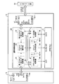
- FIG. 1 is a schematic configuration block diagram of a process control system 10 having an information processing apparatus according to an embodiment.
- FIG. 2 is a schematic configuration block diagram of the host controller 11 and the intelligent input / output device 12.
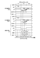
- FIG. 3 is a processing timing chart illustrating an example in which the master input / output device performs data read processing in the T2 phase by the master MPU 11A and the master MPU 23-1.
- FIG. 4 is a processing timing chart as an example of the case where the master input / output device performs data write processing in the master MPU 11A and the master MPU 23-1 in the T2 phase.
- FIG. 5 is an explanatory diagram of an access pattern analysis table.
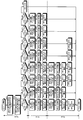
- FIG. 6 is a process flowchart of the intelligent input / output device 12.
- FIG. 1 is a schematic configuration block diagram of a process control system 10 having an information processing apparatus according to an embodiment.
- the process control system 10 includes a host controller 11 that performs overall control of the entire process control system 10, an intelligent input / output device 12 that performs input / output control under the control of the host controller 11, and input / output interfaces I11 to I1n.
- the interface unit 13 includes interface units I21 to I2n and controlled devices DEV1 to DEVn connected to the interface unit 13 via the communication network 14, respectively.
- controlled devices DEV1 to DEVn include not only controlled devices such as motors and valves, but also sensor units that sense various states (current, voltage, temperature, flow rate, pressure, etc.).
- the read address / write address in the shared memory 21 is allocated in advance for each controlled device DEV1 to DEVn, and the access order is also cyclically specified in advance, so that the same controlled It is assumed that the read address or the write address is not designated redundantly for the devices DEV1 to DEVn.
- FIG. 2 is a schematic configuration block diagram of the host controller 11 and the intelligent input / output device 12.
- the host controller 11 controls the entire host controller 11 and also has a clock terminal CLK, a ready terminal RDY to which the first ready signal RDY1 is input, a chip select terminal CS, an address terminal ADR, a read terminal RD, and a write terminal.
- a master MPU 11A having a WT and a data terminal DATA is provided.
- the intelligent input / output device 12 includes a shared memory 21 that stores input / output data, a control unit (hereinafter referred to as an arbitration control circuit 22) that performs adjustment when the access of the master MPU to the shared memory 21 competes, And master MPUs 23-1 to 23-n that perform control for inputting / outputting data to / from the device DEV1.
- a control unit hereinafter referred to as an arbitration control circuit 22
- master MPUs 23-1 to 23-n that perform control for inputting / outputting data to / from the device DEV1.
- the arbitration control circuit 22 temporarily latches access data to the shared memory 21 from the master MPU 11A of the host controller 11 and the shared memory 21 from the master MPUs 23-1 to 23-n. Based on the second access temporary latch processing unit 32 that temporarily latches the access data, the access data latched in the first access temporary latch processing unit 31 and the access data latched in the second access temporary latch processing unit 32 And an access pattern analysis unit 33 that analyzes an access pattern for the shared memory 21.
- the arbitration control circuit 22 determines the address data stored in the first access temporary latch processing unit 31 or the second access temporary based on the analysis result of the access pattern analysis unit 33.
- An address switching processing unit 34 for switching to the stored address data of the latch processing unit 32 and a command output process for outputting a write command, a read command or a chip select command of the shared memory 21 based on the analysis result of the access pattern analysis unit 33
- a data switching processing unit 36 for switching the data input destination master MPU or the output destination master MPU based on the analysis result of the access pattern analysis unit 33.
- the master MPU 23-1 includes a clock terminal CLK, a ready terminal RDY to which a second ready signal RDY2 is input, a chip select terminal CS, an address terminal ADR, a read terminal RD, a write terminal WT, and a data terminal DATA. Yes.
- the access pattern of the intelligent input / output device 12 includes T1 phase to T3 phase, which are three access phases that are continuous in time.
- FIG. 3 is a processing timing chart illustrating an example in which the master input / output device performs data read processing in the T2 phase by the master MPU 11A and the master MPU 23-1.
- FIG. 4 is a process timing chart illustrating an example in which the master MPU 11A and the master MPU 23-1 each perform data write processing in the intelligent input / output device in the T2 phase.
- the T1 phase to the T3 phase each include a first subphase A0 to a third subphase A2 that are three subphases arranged in time series. Then, the access pattern is analyzed in the first subphase A0, the shared memory access process corresponding to one master MPU is performed in the second subphase A1, and the shared memory access corresponding to the other master MPU is performed in the third subphase A2. Processing is to be done.
- the subphase includes at least a number of subphases corresponding to the master MPUs that can simultaneously access the shared memory 21 in parallel. It is assumed that a phase (two in this embodiment) is provided.
- FIG. 5 is an explanatory diagram of an access pattern analysis table.
- FIG. 5 shows a case where an access pattern is analyzed in the T2 phase.
- the access pattern analysis unit 33 is in the state of the chip select terminal CS, the read terminal RD, and the write terminal WT of the master MPU 11A and the master MPU 23-1 (in the case of positive logic [high active], “1” in FIG. 3).
- the access pattern is analyzed according to the combination of “H” level shown or “L” level shown by “0” in FIG.
- the chip select terminal CS "L”
- the read terminal RD "H”
- the chip select terminal CS "L”
- the read terminal RD "H”
- the chip select terminal CS "L”
- the read terminal RD "L”
- the master MPU 11A reads data from the shared memory 21 and the master MPU 23-1 does nothing to the shared memory 21.
- the chip select terminal CS “H”
- the read terminal RD “H”
- the chip select terminal CS “L”
- the read terminal RD “H”
- the master MPU 23-1 reads data from the shared memory 21 and the master MPU 11 A does nothing to the shared memory 21.
- the chip select terminal CS "L”
- the read terminal RD "L”
- the chip select terminal CS “H”
- the read terminal RD “H”
- the chip select terminal CS “L”
- the read terminal RD “H”
- the chip select terminal CS "L”
- the read terminal RD "H”
- the chip select terminal CS “H”
- the read terminal RD “H”
- the access pattern analysis unit 33 analyzes the access pattern based on the combination of the states of the chip select terminal CS, the read terminal RD, and the write terminal WT of the master MPU 11A and the master MPU 23-1 (step S12). Subsequently, the access pattern analysis unit 33 determines whether the analyzed access pattern is an access pattern No. in which both the master MPU 11A and the master MPU 23-1 read data from the shared memory 21. It is determined whether or not 1 (step S13).
- the analyzed access pattern is the access pattern No. If it is 1 (step S13; Yes), the access pattern analysis unit 33 controls the address switching processing unit 34 in the second subphase A1 of the T2 phase (indicated by T2_A1 in FIG. 4), and the address bus Is switched to the master MPU 11A side (step S14).
- the access pattern analysis unit 33 issues (outputs) a shared memory read command corresponding to the master MPU 11A as the shared memory command output process (step S15).
- the first access temporary latch processing unit 31 reads and latches data corresponding to the read address from the shared memory 21 (step S16).
- the access pattern analysis unit 33 controls the address switching processing unit 34 to switch the address bus to the master MPU 23-1 side (step S17).
- the access pattern analysis unit 33 issues (outputs) a shared memory read command corresponding to the master MPU 23-1 as the shared memory command output process (step S18).
- the second access temporary latch processing unit 32 reads and latches data corresponding to the read address from the shared memory 21 (step S19).
- the master MPU 11A reads the data to be read from the first access temporary latch processing unit 31, and the master MPU 23-1 reads the data to be read from the second access temporary latch processing unit 32 and performs the processing in the T2 phase.
- the process ends (step S20).
- the arbitration control circuit 22 sets the first ready signal RDY1 to the “H” level from the T1 phase to the T3 phase as shown in FIG. 3 in order to allow the master MPU 11A to access the shared memory 21. Similarly, the arbitration control circuit 22 sets the second ready signal RDY2 to the “H” level from the T1 phase to the T3 phase as shown in FIG. 3 in order to allow the master MPU 23-1 to access the shared memory 21.
- the master MPU 11A recognizes that the master MPU 11A is allowed to access the shared memory 21 based on the first ready signal RDY1, and from the address terminal ADR over the T1 phase to T3 phase as shown in FIG.
- the read address 110 of the shared memory is output.
- the master MPU 23-1 recognizes that the master MPU 23-1 is permitted to access the shared memory 21 based on the second ready signal RDY2, and, as shown in FIG. 3, the address over the T1 phase to T3 phase.
- the read address 210 of the shared memory is output from the terminal ADR.
- the master MPU 23-1 sets the read signal R to the “L” level during the T2 phase in order to notify the arbitration control circuit 22 that the read preparation is completed.
- the first access temporary latch processing unit 31 of the arbitration control circuit 22 receives the address data 110 output from the address terminal ADR of the master MPU 11A in the first subphase A0 of T2 phase (indicated by T2_A0 in FIG. 6). Latch.
- the second access temporary latch processing unit 32 of the arbitration control circuit 22 latches the address data 210 output from the address terminal ADR of the master MPU 23-1.
- the access pattern analysis unit 33 analyzes the access pattern based on the combination of the states of the chip select terminal CS, the read terminal RD, and the write terminal WT of the master MPU 11A and the master MPU 23-1.
- the access pattern analysis unit 33 controls the address switching processing unit 34 to switch the address bus and data bus to the master MPU 11A side.
- the access pattern analysis unit 33 issues (outputs) a shared memory read command corresponding to the master MPU 11A as the shared memory command output process (step S15).
- the first access temporary latch processing unit 31 reads and latches the read data 112 corresponding to the read address 111 from the shared memory 21, and outputs the read data 112 to the data bus.
- the read latch data 113 is output to the data bus of the master MPU 11A in the second subphase A1 to the third subphase A2 (indicated by T2_A1 to T2_A2 in FIG. 6) of the T2 phase.
- the read latch data 113 is output to the data bus of the master MPU 11A for a period longer than the period of the predetermined data read setup time DRS with respect to the end time of the T2 phase that is the data read timing 114 of the master MPU 11A. Continue to be done. As a result, the master MPU 11A can reliably fetch the read latch data 113.
- the access pattern analysis unit 33 controls the address switching processing unit 34 in the third subphase A2 of the T2 phase (indicated by T2_A2 in FIG. 6) to switch the address bus and data bus to the master MPU 23-1 side. .
- the access pattern analysis unit 33 issues (outputs) a shared memory read command corresponding to the master MPU 23-1 as a shared memory command output process.
- the second access temporary latch processing unit 32 reads the read data 212 corresponding to the read address 211 from the shared memory 21, latches it, and outputs the read data 212 to the data bus.
- the read latch data 213 is output to the data bus of the master MPU 23-1 in the third subphase A2 of the T2 phase (indicated by T2_A1 to T2_A2 in FIG. 6).
- the master MPU 23-1 has the data bus read from the data bus of the master MPU 23-1 for a period longer than the predetermined data read setup time DRS with respect to the end time of the T 2 phase as the data read timing 214 of the master MPU 23-1.
- the latch data 213 continues to be output.
- the master MPU 23-1 can reliably fetch the read latch data 213.
- the access pattern analysis unit 33 determines that the analyzed access pattern is an access pattern No. in which both the master MPU 11A and the master MPU 23-1 write data to the shared memory 21. It is determined whether or not 2 (step S21).
- step S21 the analyzed access pattern is an access pattern No. 2 (step S21; Yes), the access pattern analysis unit 33 controls the address switching processing unit 34 in the second subphase A1 of the T2 phase to switch the address bus and the data bus to the master MPU 11A side. (Step S22).
- the access pattern analysis unit 33 issues (outputs) the shared memory write command corresponding to the master MPU 11A to the shared memory 21 as the shared memory command output process (step S23).
- the first access temporary latch processing unit 31 writes the data of the master MPU 11A in the area corresponding to the write address of the shared memory 21 (step S24).
- the access pattern analysis unit 33 controls the address switching processing unit 34 to switch the address bus and the data bus to the master MPU 23-12 side (step S25).
- the access pattern analysis unit 33 issues (outputs) a shared memory write command corresponding to the master MPU 23-1 to the shared memory 21 as a shared memory command output process (step S26).
- the second access temporary latch processing unit 32 writes the data of the master MPU 23-1 in the area corresponding to the write address of the shared memory 21 (step S27).
- the arbitration control circuit 22 sets the first ready signal RDY1 to the “H” level from the T1 phase to the T3 phase as shown in FIG. 4 in order to allow the master MPU 11A to access the shared memory 21. Similarly, the arbitration control circuit 22 sets the second ready signal RDY2 to the “H” level from the T1 phase to the T3 phase as shown in FIG. 4 in order to allow the master MPU 23-1 to access the shared memory 21.
- the master MPU 11A grasps that the master MPU 11A is permitted to access the shared memory 21 based on the first ready signal RDY1, and from the address terminal ADR over the T1 phase to T3 phase as shown in FIG.
- the shared memory write address 120 is output.
- the master MPU 11A sets the write signal W to the “L” level during the period of the T2 phase in order to notify the arbitration control circuit 22 that the preparation for writing has been completed.
- the master MPU 23-1 recognizes that the master MPU 23-1 is permitted to access the shared memory 21 based on the second ready signal RDY2, and performs addressing from the T1 phase to the T3 phase as shown in FIG.
- the shared memory write address 220 is output from the terminal ADR.
- the master MPU 23-1 sets the write signal W to the “L” level during the period of the T2 phase in order to notify the arbitration control circuit 22 that the write preparation has been completed.
- the first access temporary latch processing unit 31 of the arbitration control circuit 22 receives the address data 120 output from the address terminal ADR of the master MPU 11A in the first subphase A0 of the T2 phase (indicated by T2_A0 in FIG. 6). Latch.
- the second access temporary latch processing unit 32 of the arbitration control circuit 22 latches the address data 220 output from the address terminal ADR of the master MPU 23-1.
- the access pattern analysis unit 33 analyzes the access pattern based on the combination of the states of the chip select terminal CS, the read terminal RD, and the write terminal WT of the master MPU 11A and the master MPU 23-1.
- the access pattern analysis unit 33 controls the address switching processing unit 34 to switch the address bus and data bus to the master MPU 11A side.
- the access pattern analysis unit 33 issues (outputs) a shared memory write command corresponding to the master MPU 11A as the shared memory command output process.
- the first access temporary latch processing unit 31 outputs the write address 120 and the corresponding write data 122 to the shared memory 21 as the write address 121 and the write data 123.
- the write signal W of the shared memory 21 becomes “L” level, and the write data is written in the area corresponding to the write address 121 in the second sub-phase A1 of the T2 phase (indicated by T2_A1 in FIG. 6). 123 is written.
- the access pattern analysis unit 33 controls the address switching processing unit 34 in the third subphase A2 of the T2 phase (indicated by T2_A2 in FIG. 6) to switch the address bus and the data bus to the master MPU 23-1 side. .
- the access pattern analysis unit 33 issues (outputs) a shared memory write command corresponding to the master MPU 23-1 as a shared memory command output process.
- the second access temporary latch processing unit 32 outputs the write address 220 and the corresponding write data 222 to the shared memory 21 as the write address 221 and the write data 223.
- the write signal W of the shared memory 21 becomes “L” level, and write data is written to the area corresponding to the write address 221 in the third sub-phase A2 of the T2 phase (indicated by T2_A2 in FIG. 6). 223 is written.
- the analyzed access pattern is the access pattern No. If it is not 2 (step S21; No), the access pattern analysis unit 33 reads the analyzed access pattern from the shared memory 21 by the master MPU 11A and the master MPU 23-1 writes the data to the shared memory 21. When the access pattern No. 3 is discriminated (step S31).
- the analyzed access pattern is the access pattern No. If it is 3 (step S31; Yes), the access pattern analysis unit 33 controls the address switching processing unit 34 in the second subphase A1 of the T2 phase to switch the address bus and data bus to the master MPU 11A side. (Step S32).
- the access pattern analysis unit 33 controls the address switching processing unit 34 in the third sub-phase A2 of the T2 phase, and transfers the address bus and data bus to the second access temporary latch processing unit 32 on the master MPU 23-1 side. Switching (step S35).
- step S41 the analyzed access pattern is an access pattern No. 4 (step S41; Yes), the access pattern analysis unit 33 controls the address switching processing unit 34 in the second subphase A1 of the T2 phase, and transfers the address bus and data bus to the master MPU 23-1 side. (Step S42).
- the access pattern analysis unit 33 issues (outputs) a shared memory read command corresponding to the master MPU 23-1 as the shared memory command output process (step S43).
- the second access temporary latch processing unit 32 reads and latches data corresponding to the read address from the shared memory 21 (step S44).
- the access pattern analysis unit 33 issues (outputs) a shared memory write command corresponding to the master MPU 11A to the shared memory 21 (step S46).
- the first access temporary latch processing unit 31 writes the data of the master MPU 11A in the area corresponding to the write address of the shared memory 21 (step S47).
- the master MPU 11A reads the data to be read from the second access temporary latch processing unit 32 and ends the process in the T2 phase (step S48).
- step S41 the analyzed access pattern is an access pattern No. If it is not 4 (step S41; No), the access pattern analysis unit 33 reads the access pattern analyzed by the master MPU 11A from the shared memory 21, and the master MPU 23-1 does nothing to the shared memory 21. When the access pattern No. Whether it is 5 or not is discriminated (step S51).
- the analyzed access pattern is the access pattern No. If it is 5 (step S51; Yes), the access pattern analysis unit 33 controls the address switching processing unit 34 in the second subphase A1 of the T2 phase to switch the address bus and data bus to the master MPU 11A side. (Step S52).
- the access pattern analysis unit 33 issues (outputs) a shared memory read command corresponding to the master MPU 11A as the shared memory command output process (step S53).
- the first access temporary latch processing unit 31 reads and latches data corresponding to the read address from the shared memory 21 (step S54).
- the master MPU 11A reads the data to be read from the first access temporary latch processing unit 31, and ends the process in the T2 phase (step S55).
- the analyzed access pattern is the access pattern No. If it is not 5 (step S51; No), the access pattern analysis unit 33 reads the access pattern analyzed by the master MPU 23-1 from the shared memory 21, and the master MPU 11A does nothing to the shared memory 21. When the access pattern No. 6 is discriminated (step S61).
- step S61 the analyzed access pattern is an access pattern No. 6 (step S61; Yes), the access pattern analysis unit 33 controls the address switching processing unit 34 in the second subphase A1 of the T2 phase, and transfers the address bus and data bus to the master MPU 23-1 side. (Step S62).
- the access pattern analysis unit 33 issues (outputs) a shared memory read command corresponding to the master MPU 23-1 as the shared memory command output process (step S63).
- the second access temporary latch processing unit 32 reads and latches data corresponding to the read address from the shared memory 21 (step S64).
- the master MPU 23-1 reads the data to be read from the second access temporary latch processing unit 32 and ends the process in the T2 phase (step S65).
- step S61 the analyzed access pattern is an access pattern No. If it is not 6 (step S61; No), the access pattern analysis unit 33 writes the analyzed access pattern into the shared memory 21 by the master MPU 11A, and the master MPU 23-1 Access pattern no. 7 is discriminated (step S71).
- step S71 the analyzed access pattern is the access pattern No. If it is 7 (step S71; Yes), the access pattern analysis unit 33 controls the address switching processing unit 34 in the second subphase A1 of the T2 phase to switch the address bus and data bus to the master MPU 11A side. (Step S72).
- the access pattern analysis unit 33 issues (outputs) the shared memory write command corresponding to the master MPU 11A to the shared memory 21 as the shared memory command output process (step S73).
- the first access temporary latch processing unit 31 writes the data of the master MPU 11A in the area corresponding to the write address of the shared memory 21, and ends the process in the T2 phase (step S74).
- the access pattern analysis unit 33 issues (outputs) the shared memory write command corresponding to the master MPU 23-1 to the shared memory 21 as the shared memory command output process (step S83).
- the second access temporary latch processing unit 32 writes the data of the master MPU 23-1 in the area corresponding to the write address of the shared memory 21, and ends the process in the T2 phase (step S84).
- the program executed by the information processing apparatus of the present embodiment is a file in an installable format or an executable format and is a computer such as a CD-ROM, a flexible disk (FD), a CD-R, a DVD (Digital Versatile Disk). It is recorded on a readable recording medium and provided.
Landscapes
- Engineering & Computer Science (AREA)
- Theoretical Computer Science (AREA)
- Physics & Mathematics (AREA)
- General Engineering & Computer Science (AREA)
- General Physics & Mathematics (AREA)
- Multi Processors (AREA)
- Programmable Controllers (AREA)
Abstract
Description
このインテリジェント入出力装置においては、被制御装置に対応する入出力データの処理をそれぞれ行う一又は複数のマスタMPUと、上位制御装置のマスタMPUとの間で入出力データの受け渡しを行うための共有メモリと、入出力データの処理を行うマスタMPU及び上位制御装置のマスタMPUを共有メモリに接続する回路と、を備えている。
そして、制御部は、同一のアクセスフェーズにおいて、n個のMPUから並行して受け付けた共有メモリへのアクセス要求に基づいて、共有メモリに対するアクセスパターンを解析し、解析したアクセスパターンに基づく順番で受け付けたm個(m:n以下の自然数)のアクセス要求をアクセスフェーズ内で順次処理する。
図1は、実施形態の情報処理装置を有するプロセス制御システム10の概要構成ブロック図である。
プロセス制御システム10は、プロセス制御システム10全体の統括制御を行う上位コントローラ11と、上位コントローラ11の制御下で、入出力制御を行うインテリジェント入出力装置12と、入出力インタフェースI11~I1nを備えたインタフェース部13と、それぞれが対応するインタフェース部I21~I2n及び通信ネットワーク14を介してインタフェース部13に接続された被制御装置DEV1~DEVnと、を備えている。
上位コントローラ11は、上位コントローラ11全体を制御するとともに、クロック端子CLK、第1レディ信号RDY1が入力されるレディ(Ready)端子RDY、チップセレクト端子CS、アドレス端子ADR、読出端子RD、書込端子WT及びデータ端子DATAを備えたマスタMPU11Aを備えている。
インテリジェント入出力装置12のアクセスパターンは、時間的に連続する三つのアクセスフェーズであるT1フェーズ~T3フェーズを備えている。
また、図4は、インテリジェント入出力装置がT2フェーズにおいてマスタMPU11A及びマスタMPU23-1がそれぞれデータ書込処理を行う場合を例とした処理タイミングチャートである。
図5は、アクセスパターン解析テーブルの説明図である。
図5においては、T2フェーズでアクセスパターンを解析する場合について示している。
共有メモリ21のアクセスパターンとしては、図2の装置構成の場合、以下の9パターンが存在している。
ここで、アクセスパターン解析部33は、マスタMPU11A及びマスタMPU23-1のチップセレクト端子CS、読出端子RD及び書込端子WTの状態(正論理[ハイアクティブ]の場合、図3中“1”で示す“H”レベル又は図3中“0”で示す“L”レベル)の組合せに応じてアクセスパターンを解析することとなる。
マスタMPU11A及びマスタMPU23-1の双方とも共有メモリ21からデータ読み出しを行う場合。
マスタMPU11A及びマスタMPU23-1の双方とも共有メモリ21にデータ書き込みを行う場合。
マスタMPU11Aが共有メモリ21からデータ読み出しを行い、マスタMPU23-1が共有メモリ21にデータ書き込みを行う場合。
マスタMPU11Aが共有メモリ21にデータ書き込みを行い、マスタMPU23-1が共有メモリ21からデータ読み出しを行う場合。
マスタMPU11Aが共有メモリ21からデータ読み出しを行い、マスタMPU23-1は共有メモリ21に対して何も行わない場合。
マスタMPU23-1が共有メモリ21からデータ読み出しを行い、マスタMPU11Aは共有メモリ21に対して何も行わない場合。
マスタMPU11Aが共有メモリ21にデータ書き込みを行い、マスタMPU23-1は共有メモリ21に対して何も行わない場合。
マスタMPU23-1が共有メモリ21にデータ書き込みを行い、マスタMPU11Aは共有メモリ21に対して何も行わない場合。
マスタMPU23-1及びマスタMPU11Aの双方とも共有メモリ21に対して何も行わない場合。
図6においては、図示の簡略化のため、マスタMPU11Aを「MPU1」と表記し、マスタMPU23-1を「MPU2」と表記している。
まず、調停制御回路22の第1アクセス一時ラッチ処理部31は、T2フェーズの第1サブフェーズA0(図4中、T2_A0で示す)において、マスタMPU11Aのアドレス端子ADRから出力されるアドレスデータ及びデータ端子DATAから出力される書き込みデータをラッチする。一方、調停制御回路22の第2アクセス一時ラッチ処理部32は、マスタMPU23-1のアドレス端子ADRから出力されるアドレスデータ及びデータ端子DATAから出力される書き込みデータをラッチする(ステップS11)。
続いて、アクセスパターン解析部33は、解析したアクセスパターンが、マスタMPU11A及びマスタMPU23-1の双方とも共有メモリ21からデータ読み出しを行う場合であるアクセスパターンNo.1であるか否かを判別する(ステップS13)。
この結果、第2アクセス一時ラッチ処理部32は、読出アドレスに対応するデータを共有メモリ21から読み出し、ラッチすることとなる(ステップS19)。
調停制御回路22は、マスタMPU11Aに共有メモリ21に対するアクセスを許可すべく、第1レディ信号RDY1を、図3に示すようにT1フェーズ~T3フェーズにわたって“H”レベルとする。同様に調停制御回路22は、マスタMPU23-1に共有メモリ21に対するアクセスを許可すべく、第2レディ信号RDY2を、図3に示すようにT1フェーズ~T3フェーズにわたって“H”レベルとする。
一方、調停制御回路22の第1アクセス一時ラッチ処理部31は、T2フェーズの第1サブフェーズA0(図6中、T2_A0で示す)において、マスタMPU11Aのアドレス端子ADRから出力されるアドレスデータ110をラッチする。また、調停制御回路22の第2アクセス一時ラッチ処理部32は、マスタMPU23-1のアドレス端子ADRから出力されるアドレスデータ210をラッチする。
ステップS13の判別において、解析したアクセスパターンがアクセスパターンNo.1ではない場合には(ステップS13;No)、アクセスパターン解析部33は、解析したアクセスパターンがマスタMPU11A及びマスタMPU23-1の双方とも共有メモリ21にデータ書き込みを行う場合であるアクセスパターンNo.2であるか否かを判別する(ステップS21)。
この結果、第1アクセス一時ラッチ処理部31は、共有メモリ21の書込アドレスに対応する領域にマスタMPU11Aのデータを書き込むこととなる(ステップS24)。
続いて、アクセスパターン解析部33は、T2フェーズの第3サブフェーズA2において、アドレス切換処理部34を制御し、アドレスバス及びデータバスをマスタMPU23-12側に切り替える(ステップS25)。
この結果、第2アクセス一時ラッチ処理部32は、共有メモリ21の書込アドレスに対応する領域にマスタMPU23-1のデータを書き込むこととなる(ステップS27)。
調停制御回路22は、マスタMPU11Aに共有メモリ21に対するアクセスを許可すべく、第1レディ信号RDY1を、図4に示すようにT1フェーズ~T3フェーズにわたって“H”レベルとする。同様に調停制御回路22は、マスタMPU23-1に共有メモリ21に対するアクセスを許可すべく、第2レディ信号RDY2を、図4に示すようにT1フェーズ~T3フェーズにわたって“H”レベルとする。
一方、調停制御回路22の第1アクセス一時ラッチ処理部31は、T2フェーズの第1サブフェーズA0(図6中、T2_A0で示す)において、マスタMPU11Aのアドレス端子ADRから出力されるアドレスデータ120をラッチする。また、調停制御回路22の第2アクセス一時ラッチ処理部32は、マスタMPU23-1のアドレス端子ADRから出力されるアドレスデータ220をラッチする。
ステップS21の判別において、解析したアクセスパターンがアクセスパターンNo.2ではない場合には(ステップS21;No)、アクセスパターン解析部33は、解析したアクセスパターンが、マスタMPU11Aが共有メモリ21からデータ読み出しを行い、マスタMPU23-1が共有メモリ21にデータ書き込みを行う場合であるアクセスパターンNo.3であるか否かを判別する(ステップS31)。
この結果、第1アクセス一時ラッチ処理部31は、読出アドレスに対応するデータを共有メモリ21から読み出し、ラッチすることとなる(ステップS34)。
この結果、第2アクセス一時ラッチ処理部32は、共有メモリ21の書込アドレスに対応する領域にマスタMPU23-1のデータを書き込むこととなる(ステップS37)。
この結果、第2アクセス一時ラッチ処理部32は、読出アドレスに対応するデータを共有メモリ21から読み出し、ラッチすることとなる(ステップS44)。
この結果、第1アクセス一時ラッチ処理部31は、共有メモリ21の書込アドレスに対応する領域にマスタMPU11Aのデータを書き込むこととなる(ステップS47)。
この結果、第1アクセス一時ラッチ処理部31は、読出アドレスに対応するデータを共有メモリ21から読み出し、ラッチすることとなる(ステップS54)。
この結果、第2アクセス一時ラッチ処理部32は、読出アドレスに対応するデータを共有メモリ21から読み出し、ラッチすることとなる(ステップS64)。
この結果、第1アクセス一時ラッチ処理部31は、共有メモリ21の書込アドレスに対応する領域にマスタMPU11Aのデータを書き込み、当該T2フェーズにおける処理を終了することとなる(ステップS74)。
この結果、第2アクセス一時ラッチ処理部32は、共有メモリ21の書込アドレスに対応する領域にマスタMPU23-1のデータを書き込み、当該T2フェーズにおける処理を終了することとなる(ステップS84)。
また、本実施形態の情報処理装置のプログラムを、ROM等に予め組み込んで提供するように構成してもよい。
Claims (7)
- n個(n:2以上の整数)のMPUの共有メモリへのアクセスを制御する情報処理装置において、
同一のアクセスフェーズにおいて、前記n個のMPUから並行して受け付けた前記共有メモリへのアクセス要求に基づいて、前記共有メモリに対するアクセスパターンを解析し、前記解析したアクセスパターンに基づく順番で前記受け付けたm個(m:n以下の自然数)のアクセス要求を前記アクセスフェーズ内で順次処理する制御部を備えた情報処理装置。 - 前記制御部は、前記MPUからの前記アクセス要求及び前記アクセス要求に対応するデータをそれぞれ格納可能な複数のラッチ処理部と、
前記n個のMPUから並行して受け付けた前記共有メモリへのアクセス要求に基づいて、前記共有メモリに対する前記複数のMPUのアクセスパターンを解析するアクセスパターン解析部と、
前記アクセスパターンの解析結果に基づいて、前記共有メモリにアクセスコマンドの出力を行うコマンド出力処理部と、
を備えた請求項1記載の情報処理装置。 - 前記制御部は、前記アクセスパターンの解析結果に基づいて、前記n個のMPUのうち処理対象のいずれかのMPUのアクセス要求に対応するアドレスデータを前記共有メモリに出力するアドレス切換処理部と、
前記アクセスパターンの解析結果に基づいて、前記n個のMPUのうち処理対象のいずれかのMPUのアクセス要求に対応する書込データを前記共有メモリに出力し、あるいは、前記n個のMPUのうち処理対象のいずれかのMPUのアクセス要求に対応する読出データを前記共有メモリから読み出すデータ切換処理部と、
を備えた請求項2記載の情報処理装置。 - 前記アクセスフェーズは、少なくとも(n+1)個のサブフェーズを備え、
前記制御部は、前記アクセスフェーズの最初のサブフェーズにおいて、前記アクセスパターンの解析を行い、残りのn個のサブフェーズにおいて、前記m個のアクセス要求を順次処理する、
請求項1乃至請求項3のいずれか一項に記載の情報処理装置。 - 前記n個のMPUのうち、いずれか少なくとも一つは、上位コントローラを構成するMPUで有り、
前記n個のMPUのうち、前記上位コントローラを構成するMPU以外のMPUは、当該情報処理装置を構成するとともに、前記上位コントローラの制御下で、対応する被制御装置をそれぞれ制御するMPUである、
請求項1乃至請求項4のいずれか一項に記載の情報処理装置。 - n個(n:2以上の整数)のMPUの共有メモリへのアクセスを制御する情報処理装置で実行される方法であって、
同一のアクセスフェーズにおいて、前記n個のMPUから並行して前記共有メモリへのアクセス要求を受け付ける過程と、
前記アクセス要求に基づいて、前記共有メモリに対するアクセスパターンを解析する過程と、
前記解析したアクセスパターンに基づく順番で前記受け付けたm個(m:n以下の自然数)のアクセス要求を前記アクセスフェーズ内で順次処理する過程と、
を備えた方法。 - n個(n:2以上の整数)のMPUの共有メモリへのアクセスを制御する情報処理装置をコンピュータにより制御するためのプログラムであって、
前記コンピュータを、
同一のアクセスフェーズにおいて、前記n個のMPUから並行して前記共有メモリへのアクセス要求を受け付ける手段と、
前記アクセス要求に基づいて、前記共有メモリに対するアクセスパターンを解析する手段と、
前記解析したアクセスパターンに基づく順番で前記受け付けたm個(m:n以下の自然数)のアクセス要求を前記アクセスフェーズ内で順次処理する手段と、
して機能させるプログラム。
Priority Applications (3)
| Application Number | Priority Date | Filing Date | Title |
|---|---|---|---|
| KR1020177035176A KR20180005205A (ko) | 2015-07-10 | 2016-03-25 | 정보 처리 장치, 방법 및 프로그램 |
| CN201680033224.XA CN107636622A (zh) | 2015-07-10 | 2016-03-25 | 信息处理装置、方法以及程序 |
| SG11201800088RA SG11201800088RA (en) | 2015-07-10 | 2016-03-25 | Information processing device, method, and program |
Applications Claiming Priority (2)
| Application Number | Priority Date | Filing Date | Title |
|---|---|---|---|
| JP2015-138974 | 2015-07-10 | ||
| JP2015138974A JP2017021589A (ja) | 2015-07-10 | 2015-07-10 | 情報処理装置、方法及びプログラム |
Publications (1)
| Publication Number | Publication Date |
|---|---|
| WO2017010127A1 true WO2017010127A1 (ja) | 2017-01-19 |
Family
ID=57758018
Family Applications (1)
| Application Number | Title | Priority Date | Filing Date |
|---|---|---|---|
| PCT/JP2016/059712 Ceased WO2017010127A1 (ja) | 2015-07-10 | 2016-03-25 | 情報処理装置、方法及びプログラム |
Country Status (6)
| Country | Link |
|---|---|
| JP (1) | JP2017021589A (ja) |
| KR (1) | KR20180005205A (ja) |
| CN (1) | CN107636622A (ja) |
| SG (1) | SG11201800088RA (ja) |
| TW (1) | TW201706846A (ja) |
| WO (1) | WO2017010127A1 (ja) |
Families Citing this family (3)
| Publication number | Priority date | Publication date | Assignee | Title |
|---|---|---|---|---|
| KR102223912B1 (ko) | 2019-01-10 | 2021-03-08 | 한국전자통신연구원 | 다중 뉴럴 네트워크를 이용한 문자 인식을 위한 장치 및 그것의 동작 방법 |
| CN111338243A (zh) * | 2020-02-21 | 2020-06-26 | 江苏大量度电气科技有限公司 | 一种电气设备终端智能控制方法及系统 |
| CN111984410A (zh) * | 2020-08-18 | 2020-11-24 | 上海睿赛德电子科技有限公司 | 一种在嵌入式系统中低资源占用的内存保护系统 |
Citations (2)
| Publication number | Priority date | Publication date | Assignee | Title |
|---|---|---|---|---|
| JPH0333966A (ja) * | 1989-06-29 | 1991-02-14 | Nec Corp | メモリ制御回路 |
| JP2000194683A (ja) * | 1998-12-28 | 2000-07-14 | Nec Kofu Ltd | 共有メモリの調停回路およびその調停方法 |
-
2015
- 2015-07-10 JP JP2015138974A patent/JP2017021589A/ja not_active Abandoned
-
2016
- 2016-03-25 KR KR1020177035176A patent/KR20180005205A/ko not_active Withdrawn
- 2016-03-25 SG SG11201800088RA patent/SG11201800088RA/en unknown
- 2016-03-25 WO PCT/JP2016/059712 patent/WO2017010127A1/ja not_active Ceased
- 2016-03-25 CN CN201680033224.XA patent/CN107636622A/zh not_active Withdrawn
- 2016-05-23 TW TW105115986A patent/TW201706846A/zh unknown
Patent Citations (2)
| Publication number | Priority date | Publication date | Assignee | Title |
|---|---|---|---|---|
| JPH0333966A (ja) * | 1989-06-29 | 1991-02-14 | Nec Corp | メモリ制御回路 |
| JP2000194683A (ja) * | 1998-12-28 | 2000-07-14 | Nec Kofu Ltd | 共有メモリの調停回路およびその調停方法 |
Also Published As
| Publication number | Publication date |
|---|---|
| KR20180005205A (ko) | 2018-01-15 |
| SG11201800088RA (en) | 2018-02-27 |
| CN107636622A (zh) | 2018-01-26 |
| JP2017021589A (ja) | 2017-01-26 |
| TW201706846A (zh) | 2017-02-16 |
Similar Documents
| Publication | Publication Date | Title |
|---|---|---|
| EP1901162A2 (en) | Storage system and data migration method for the same | |
| US8924606B2 (en) | Storage system and data transfer control method | |
| JP5852259B2 (ja) | 多重バンクへの同時に起こる読出し/書込みアクセスを提供するように構成されたメモリ | |
| JP2010134627A (ja) | バス中継装置 | |
| WO2017010127A1 (ja) | 情報処理装置、方法及びプログラム | |
| US7886097B2 (en) | Bus arbitration system, medium, and method | |
| JP4616586B2 (ja) | メモリ初期化制御装置 | |
| US20150269073A1 (en) | Compiler-generated memory mapping hints | |
| JP7408954B2 (ja) | メモリ制御方法、メモリ制御装置、プログラム | |
| US20130238881A1 (en) | Data transmission device, data transmission method, and computer program product | |
| JP7225904B2 (ja) | ベクトル演算処理装置、ベクトル演算処理装置による配列変数初期化方法、及び、ベクトル演算処理装置による配列変数初期化プログラム | |
| CN115427938B (zh) | 使用复合存储器命令的存储器操作 | |
| KR101242195B1 (ko) | 페이지의 물리적 저장 위치의 변경이 가능한 스토리지 시스템 및 상기 스토리지 시스템의 동작 방법 | |
| JP6204044B2 (ja) | 不揮発性記憶システム、不揮発性記憶装置、および、メモリコントローラ | |
| JP4622871B2 (ja) | データ処理システム、アクセス制御方法、その装置およびそのプログラム | |
| JP4790540B2 (ja) | 半導体装置 | |
| JP4640272B2 (ja) | ポート制御装置 | |
| JP4925162B2 (ja) | メモリ装置 | |
| JP4468666B2 (ja) | 二重書込機能を有する装置およびストレージ制御装置 | |
| US20100254037A1 (en) | Information processing system and method for accessing information processing device | |
| JP4512334B2 (ja) | バスブリッジ回路 | |
| JP5907109B2 (ja) | 切り替え装置、この装置を搭載した記憶システム、切り替え方法および切り替えプログラム | |
| JP6099846B2 (ja) | 演算ユニット、エンジニアリングツール及びエンジニアリングツールプログラム | |
| JP4750620B2 (ja) | 階層型ストレージ装置のデータリード方法及びシステム | |
| JP2016151803A (ja) | ストレージ制御装置、ストレージ制御プログラム、およびストレージ制御方法 |
Legal Events
| Date | Code | Title | Description |
|---|---|---|---|
| 121 | Ep: the epo has been informed by wipo that ep was designated in this application |
Ref document number: 16824108 Country of ref document: EP Kind code of ref document: A1 |
|
| ENP | Entry into the national phase |
Ref document number: 20177035176 Country of ref document: KR Kind code of ref document: A |
|
| WWE | Wipo information: entry into national phase |
Ref document number: 11201800088R Country of ref document: SG |
|
| NENP | Non-entry into the national phase |
Ref country code: DE |
|
| 122 | Ep: pct application non-entry in european phase |
Ref document number: 16824108 Country of ref document: EP Kind code of ref document: A1 |