WO2017006946A1 - Dispositif de transmission d'énergie, dispositif de réception d'énergie, et système d'alimentation en énergie sans contact - Google Patents
Dispositif de transmission d'énergie, dispositif de réception d'énergie, et système d'alimentation en énergie sans contact Download PDFInfo
- Publication number
- WO2017006946A1 WO2017006946A1 PCT/JP2016/069947 JP2016069947W WO2017006946A1 WO 2017006946 A1 WO2017006946 A1 WO 2017006946A1 JP 2016069947 W JP2016069947 W JP 2016069947W WO 2017006946 A1 WO2017006946 A1 WO 2017006946A1
- Authority
- WO
- WIPO (PCT)
- Prior art keywords
- power
- power transmission
- circuit
- metal plate
- side coil
- Prior art date
Links
Images


Classifications
-
- H—ELECTRICITY
- H01—ELECTRIC ELEMENTS
- H01F—MAGNETS; INDUCTANCES; TRANSFORMERS; SELECTION OF MATERIALS FOR THEIR MAGNETIC PROPERTIES
- H01F38/00—Adaptations of transformers or inductances for specific applications or functions
- H01F38/14—Inductive couplings
-
- H—ELECTRICITY
- H02—GENERATION; CONVERSION OR DISTRIBUTION OF ELECTRIC POWER
- H02J—CIRCUIT ARRANGEMENTS OR SYSTEMS FOR SUPPLYING OR DISTRIBUTING ELECTRIC POWER; SYSTEMS FOR STORING ELECTRIC ENERGY
- H02J50/00—Circuit arrangements or systems for wireless supply or distribution of electric power
- H02J50/10—Circuit arrangements or systems for wireless supply or distribution of electric power using inductive coupling
- H02J50/12—Circuit arrangements or systems for wireless supply or distribution of electric power using inductive coupling of the resonant type
-
- H—ELECTRICITY
- H02—GENERATION; CONVERSION OR DISTRIBUTION OF ELECTRIC POWER
- H02J—CIRCUIT ARRANGEMENTS OR SYSTEMS FOR SUPPLYING OR DISTRIBUTING ELECTRIC POWER; SYSTEMS FOR STORING ELECTRIC ENERGY
- H02J50/00—Circuit arrangements or systems for wireless supply or distribution of electric power
- H02J50/60—Circuit arrangements or systems for wireless supply or distribution of electric power responsive to the presence of foreign objects, e.g. detection of living beings
-
- H—ELECTRICITY
- H02—GENERATION; CONVERSION OR DISTRIBUTION OF ELECTRIC POWER
- H02J—CIRCUIT ARRANGEMENTS OR SYSTEMS FOR SUPPLYING OR DISTRIBUTING ELECTRIC POWER; SYSTEMS FOR STORING ELECTRIC ENERGY
- H02J7/00—Circuit arrangements for charging or depolarising batteries or for supplying loads from batteries
-
- H—ELECTRICITY
- H04—ELECTRIC COMMUNICATION TECHNIQUE
- H04M—TELEPHONIC COMMUNICATION
- H04M1/00—Substation equipment, e.g. for use by subscribers
- H04M1/02—Constructional features of telephone sets
- H04M1/04—Supports for telephone transmitters or receivers
Definitions
- the present invention relates to a power transmission device, a power reception device, and a non-contact power supply system.
- NFC Near Field Communication
- 13.56 MHz 13.56 MHz
- a technique for performing non-contact power feeding by a magnetic field resonance method using a coil used for NFC communication has also been proposed.
- a power transmission side resonance circuit including a power transmission side coil is disposed in a power supply device, and a power reception side resonance circuit including a power reception side coil is disposed in an electronic device as a power reception device.
- a common reference frequency is set to a common reference frequency.
- an alternating current of the reference frequency is generated in the power transmission side coil by passing an alternating current through the power transmission side coil.
- this alternating magnetic field is transmitted to the power receiving side resonance circuit that resonates at the reference frequency, and an alternating current flows through the power receiving side coil. That is, power is transmitted from the power transmission side resonance circuit including the power transmission side coil to the power reception side resonance circuit including the power reception side coil.
- the foreign object here is, for example, an object (such as a card) having a wireless IC tag having an antenna coil of 13.56 MHz that does not respond to NFC communication.
- the foreign object is an electronic device that has the NFC communication function itself but is disabled.
- a smartphone that has an NFC communication function but whose function is turned off by software setting can be a foreign object.
- the smartphone without the power receiving function is classified as a foreign object.
- the foreign object When the power transmission operation is performed, if such a foreign object is placed on the power supply stand, the foreign object may be destroyed by the strong magnetic field generated by the power transmission side coil.
- a strong magnetic field during a power transmission operation may increase the terminal voltage of a foreign object coil on the power supply base from 100 V to 200 V. If no foreign object is formed to withstand such a high voltage, Is destroyed.
- an iron plate etc. can also become a foreign material.
- a foreign substance such as an iron plate may generate heat due to the magnetic field generated by the power transmission side coil. If the heat generation is a problem, it is necessary to cope with it.
- a metal plate made of aluminum or the like may be provided from the viewpoint of improving structural strength and texture.
- an opening is provided in the metal plate at a position opposite to the position where the power reception side coil is arranged, and during power transmission / reception, the power transmission side coil and the power reception side coil are passed through the opening. Will face each other.
- the metal plate having the opening acts to change the resonance frequency of each resonance circuit through magnetic coupling with the coil. This change is undesirable for a system that attempts to transmit and receive power at the reference frequency.
- An object of the present invention is to provide a power transmission device and a non-contact power feeding system that contribute to prevention of damage to foreign matters.
- an object of the present invention is to provide a power receiving device and a non-contact power feeding system that contribute to the realization of good power reception and power transmission / reception.
- a first power transmission device includes a power transmission side resonance including a power transmission side coil for transmitting the power in a power transmission device capable of transmitting power to the power reception device as the first power reception device by a magnetic resonance method.
- a power transmission circuit that can supply an AC voltage to the power transmission side resonance circuit, a detection circuit that detects an amplitude of a current flowing through the power transmission side coil, and the power transmission circuit to control power transmission.
- a control circuit wherein the control circuit controls the continuation of the power transmission based on the amplitude detection value of the detection circuit when the power is being transmitted.
- the control circuit monitors whether or not the amplitude detection value of the detection circuit is out of a predetermined range when the power is transmitted. Thus, it is preferable to control the continuation of the power transmission.
- the control circuit detects a deviation from the predetermined range of the amplitude detection value of the detection circuit when the power is transmitted. At this time, the power transmission may be stopped.
- the control circuit determines whether an amplitude detection value of the detection circuit deviates from the predetermined range when the power is transmitted.
- the power transmission may be stopped when it is determined that there is a foreign object that is different from the power receiving apparatus and can generate a current based on the magnetic field generated by the power transmission side coil.
- the control circuit determines whether the amplitude detection value of the detection circuit exceeds an upper limit value of the predetermined range when the power is transmitted. By doing so, it is preferable to determine whether or not there is a foreign matter including a coil as the foreign matter.
- the power reception device includes a power reception side resonance circuit including a power reception side coil for receiving the power, and the power reception side resonance circuit of the power reception side resonance circuit prior to power reception.
- a change / short circuit for changing a resonance frequency from a resonance frequency at the time of power reception or short-circuiting the power-receiving side coil, and the control circuit is configured to perform the control on the power reception device according to a signal from the power transmission device.
- a first control circuit that controls the power transmission circuit so that a predetermined test magnetic field is generated in the power transmission side coil prior to the power transmission in a state where the resonance frequency of the power reception side resonance circuit is changed or the power reception side coil is short-circuited.
- a third processing unit that realizes the power transmission by controlling the power transmission circuit so that a power transmission magnetic field larger than the test magnetic field is generated in the power transmission side coil later, and the detection circuit includes the power transmission.
- the amplitude is detected through a process of amplifying a signal indicating the amplitude of the current flowing in the side coil, and the amplification factor in the amplification is higher than that when the test magnetic field is generated in the power transmission side coil. It is better if the power transmission magnetic field is generated by the side coil.
- a first non-contact power feeding system includes a power transmission device having a power transmission side resonance circuit including a power transmission side coil for transmitting power, and a power reception side resonance circuit including a power reception side coil for receiving the power.
- a non-contact power feeding system capable of transmitting and receiving the power by a magnetic resonance method, wherein the power transmission device is capable of supplying an AC voltage to the power transmission resonance circuit, and the power transmission
- a detection circuit that detects an amplitude of a current flowing through the side coil, and a control circuit that controls power transmission by controlling the power transmission circuit, and the control circuit is configured to transmit power. In this case, the continuation of the power transmission is controlled based on the amplitude detection value of the detection circuit.
- the control circuit determines whether or not an amplitude detection value of the detection circuit deviates from a predetermined range when the power is transmitted. It is preferable to control the continuation of the power transmission by monitoring.
- the control circuit detects a deviation of the amplitude detection value of the detection circuit from the predetermined range when the power is transmitted. When done, the power transmission should be stopped.
- the control circuit determines whether or not an amplitude detection value of the detection circuit is out of the predetermined range when the power is transmitted.
- the control circuit determines whether or not the amplitude detection value of the detection circuit exceeds an upper limit value of the predetermined range when the power is transmitted. It is preferable to determine whether or not there is a foreign matter including a coil as the foreign matter.
- the power receiving device changes a resonance frequency of the power reception side resonance circuit from a resonance frequency at the time of power reception or power reception side coil prior to power reception.
- the control circuit is provided with a change / short circuit for short-circuiting, and the control circuit is configured to change the resonance frequency of the power-receiving-side resonance circuit or short-circuit the power-receiving-side coil in the power receiving device in accordance with a signal from the power transmission device.
- a first processing unit that controls the power transmission circuit so that a predetermined test magnetic field is generated by the power transmission coil prior to the power transmission, and an amplitude detection value of the detection circuit when the test magnetic field is generated
- a second processing unit that determines whether or not the power transmission can be performed based on the power transmission side coil, and a power transmission magnetic field larger than the test magnetic field after the power transmission is determined to be performed by the power transmission side coil.
- a third processing unit that realizes the power transmission by controlling the power transmission circuit to be generated, and the detection circuit undergoes a process of amplifying a signal indicating an amplitude of a current flowing through the power transmission side coil. The amplitude is detected, and the amplification factor in the amplification is higher when the power transmission side coil generates the power transmission magnetic field than when the power transmission side coil generates the test magnetic field. The smaller is better.
- a second power receiving device receives the power in a power receiving device capable of receiving the power by a magnetic field resonance method from a power transmitting device having a power transmitting side resonance circuit including a power transmitting side coil for transmitting power.
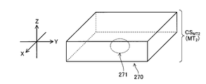
- a power receiving side resonance circuit including a power receiving side coil and a metal part having a metal plate provided with an opening at a position opposite to the position where the power receiving side coil is disposed. The opening is located between the power transmission side coil and the power reception side coil, and the resonance frequency of the power reception side resonance circuit and the resonance of the power transmission side resonance circuit.
- a magnetic part is provided at a position that affects at least one of the frequencies.
- the magnetic body portion may include an in-opening magnetic body disposed in the opening.
- the magnetic substance in the opening cancels the change in the resonance frequency of the power receiving side resonance circuit by the metal plate, and the metal plate by the metal plate in the predetermined positional relationship. It is preferable to cancel the change in the resonance frequency of the power transmission side resonance circuit.
- a distance between the power receiving side coil and the opening inner magnetic body may be equal to a distance between the power transmission side coil and the opening inner magnetic body.
- the opening is preferably sealed by the magnetic substance in the opening.
- the magnetic material in the opening is a magnetic plate fitted in the opening, and one surface of the magnetic plate and one surface of the metal plate are the same plane.
- the other surface of the magnetic plate and the other surface of the metal plate are preferably positioned on the same plane parallel to the plane.
- the power receiving side coil is disposed between the magnetic body portion and the metal plate, and the power transmission / reception is performed by the power transmitting side resonance circuit and the power receiving side resonance circuit.
- the magnetic body portion cancels a change from the reference frequency of the resonance frequency of the power-receiving-side resonance circuit caused by the metal plate in the predetermined positional relationship.
- the resonance frequency of the power transmission side resonance circuit may become the reference frequency by changing the resonance frequency of the power transmission side resonance circuit under the influence of the metal plate.
- an electronic circuit including an integrated circuit may be provided on the opposite side of the magnetic body portion from the power receiving side coil.
- the metal plate is disposed between the power receiving side coil and the magnetic body portion, and the power transmission / reception is performed by the power transmitting side resonance circuit and the power receiving side resonance.
- the circuit is performed in a state where each resonance frequency of the circuit is set to a predetermined reference frequency, and the magnetic body portion cancels a change from the reference frequency in the resonance frequency of the power transmission side resonance circuit by the metal plate in the predetermined positional relationship.
- the resonance frequency of the power reception side resonance circuit may be the reference frequency by changing the resonance frequency of the power reception side resonance circuit under the influence of the metal plate.
- the magnetic body portion is disposed between the power receiving side coil and the metal plate, and the power transmission / reception is performed by the power transmitting side resonance circuit and the power receiving side resonance.
- Each resonance frequency of the circuit is set to a predetermined reference frequency, and the magnetic body portion cancels a change from the reference frequency of the resonance frequency of the power receiving side resonance circuit by the metal plate, and the predetermined positional relationship
- the resonance frequency of the power transmission side resonance circuit may be the reference frequency by changing the resonance frequency of the power transmission side resonance circuit under the influence of the metal plate.
- the magnetic body portion may be made of ferrite.
- the metal plate may be made of aluminum or an aluminum alloy.
- a casing of the power receiving device may be formed by the metal portion.
- a second contactless power feeding system includes a power receiving device as the second power receiving device, and a power transmitting device having a power transmitting side resonance circuit including a power transmitting side coil for transmitting power, and a magnetic field The power can be transmitted and received by a resonance method.
- the power transmission device detects a power transmission circuit capable of supplying an AC voltage to the power transmission side resonance circuit and an amplitude of a current flowing in the power transmission side coil.
- a circuit and a control circuit that performs power transmission control of the power by controlling the power transmission circuit based on an amplitude detection value of the detection circuit may be provided.
- the power receiving device changes a resonance frequency of the power receiving side resonance circuit from a resonance frequency at the time of power reception prior to receiving power from the power transmission device, or
- a change / short circuit for short-circuiting the power-receiving side coil is provided, and the control circuit is configured to change the resonance frequency of the power-receiving-side resonance circuit or to short-circuit the power-receiving-side coil in the power receiving device according to a signal from the power transmission device.
- a first processing unit that controls the power transmission circuit so that a predetermined test magnetic field is generated in the power transmission side coil prior to the power transmission, and the detection circuit when the test magnetic field is generated.
- a second processing unit that determines whether or not the power transmission can be performed based on an amplitude detection value by the power transmission, and a power transmission magnetic field that is larger than the test magnetic field after determining that the power transmission can be performed
- a third processing unit that realizes the power transmission by controlling the power transmission circuit to be generated by the power transmission side coil, and based on the magnetic field generated by the power transmission side coil, the metal plate and the magnetic body unit It is preferable that currents flow in opposite directions.
- a third power receiving device receives the power in a power receiving device capable of receiving the power by a magnetic field resonance method from a power transmitting device having a power transmitting side resonance circuit including a power transmitting side coil for transmitting power.
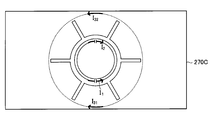
- a power receiving side resonance circuit including a power receiving side coil and a metal part having a metal plate provided with an opening at a position opposite to the position where the power receiving side coil is disposed. The opening is positioned between the power transmission side coil and the power reception side coil, and the metal plate is directed from the opening to the outer periphery of the metal plate.
- the slit portion is formed.
- the slit portion may include a cutting slit extending from the opening to the outer periphery of the metal plate.
- the metal portion includes, as the metal plate, a first metal plate provided with a first opening at a position opposite to the position where the power receiving side coil is disposed; A second metal plate provided with a second opening at a position opposite to the arrangement position of the power receiving side coil, and the first metal body and the second metal plate are coupled with an insulator interposed therebetween, and the predetermined position
- the first opening and the second opening are located between the power transmission side coil and the power reception side coil, and the slit portion serves as the cutting slit from the first opening to the first metal.
- the slit portion includes a plurality of slits formed at different positions from the opening toward the outer periphery of the metal plate, and each slit and the outer periphery of the metal plate The metal which comprises the said metal plate may remain between.
- the plurality of slits may be formed radially from the opening toward the outer periphery of the metal plate.
- the power transmission / reception is performed in a state where each resonance frequency of the power transmission side resonance circuit and the power reception side resonance circuit is set to a predetermined reference frequency, and the predetermined positional relationship
- the resonance frequencies of the power transmission side resonance circuit and the power reception side resonance circuit change under the influence of the metal plate, so that each resonance frequency of the power transmission side resonance circuit and the power reception side resonance circuit becomes the reference frequency. It would be nice.
- the metal plate is made of aluminum or an aluminum alloy.
- a casing of the power receiving device may be formed by the metal portion.
- a third non-contact power feeding system includes a power receiving device as the third power receiving device, and a power transmitting device having a power transmitting side resonance circuit including a power transmitting side coil for transmitting power, and a magnetic field The power can be transmitted and received by a resonance method.
- the power transmission device detects a power transmission circuit capable of supplying an AC voltage to the power transmission side resonance circuit and an amplitude of a current flowing in the power transmission side coil.
- a circuit and a control circuit that performs power transmission control of the power by controlling the power transmission circuit based on an amplitude detection value of the detection circuit may be provided.
- the power receiving device changes the resonance frequency of the power receiving side resonance circuit from the resonance frequency at the time of power reception prior to receiving power from the power transmission device, or A change / short circuit for short-circuiting the power-receiving side coil
- the control circuit changes the resonance frequency of the power-receiving-side resonance circuit in the power-receiving device according to a signal by communication from the power transmission device or the power-receiving-side coil.
- a second processing unit that determines whether or not the power transmission can be performed based on an amplitude detection value by a detection circuit; and for power transmission that is larger than the test magnetic field after determining that the power transmission can be performed Field is may have a third processing unit for realizing the power transmission by controlling the transmission circuit to be generated by the power transmission coil.
- the present invention it is possible to provide a power transmission device and a non-contact power supply system that contribute to prevention of damage to foreign matters. Or according to this invention, it becomes possible to provide the power receiving apparatus and non-contact electric power feeding system which contribute to realization of favorable power receiving and power transmission / reception.
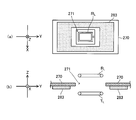
- FIG. 4 is a partial configuration diagram of a power supply device including an internal block diagram of an IC in the power supply device according to the first embodiment of the present invention.
- FIG. 3 is a partial configuration diagram of an electronic device including an internal block diagram of an IC in the electronic device according to the first embodiment of the present invention.
- FIG. 8 is a waveform diagram of a voltage drop of a sense resistor in the load detection circuit of FIG. 7.
- circuit diagrams which show an example of the resonance state change circuit which concerns on 1st Embodiment of this invention.
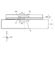
- (A)-(d) is a figure which illustrates the arrangement
- FIGS. 1-10 These are figures which concern on 2nd Embodiment of this invention and show the relationship between a X-axis, a Y-axis, a Z-axis, and a feed stand.
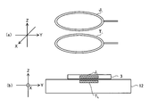
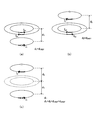
- (A) And (b) concerns on 2nd Embodiment of this invention, and is a schematic perspective view and sectional drawing of a power transmission side coil and a power receiving side coil.
- (A) And (b) concerns on 2nd Embodiment of this invention, and is a schematic perspective view and sectional drawing of a power transmission side coil and a coil of a foreign material.
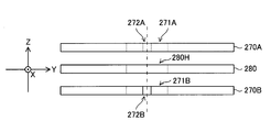
- FIG. 1 A) to (c) relate to a second embodiment of the present invention, and are a perspective view of a metal plate, a transparent view of a part of a power feeding device and an electronic device, and a plan view of a metal plate and a power receiving coil, respectively. is there.
- FIG. 1 A) to (c) relate to a second embodiment of the present invention, and are a perspective view of a metal plate, a transparent view of a part of a power feeding device and an electronic device, and a plan view of a metal plate and a power receiving coil, respectively. is there.
- These are the perspective views of the metal cases which can be provided in an electronic device concerning 2nd Embodiment of this invention.
- FIG. 1 A) to (c) relate to a second embodiment of the present invention, and are a perspective view of a metal plate, a transparent view of a part of a power feeding device and an electronic device, and a plan view of a metal plate and a power receiving coil, respectively. is there.
- FIG. (A)-(c) is a figure which shows the relationship of the electric current which concerns on 2nd Embodiment of this invention, and flows into a metal plate, a power transmission side coil, and a receiving side coil.
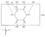
- (A) to (c) relate to an example (EX3_1) belonging to the third embodiment of the present invention, for explaining the structure and positional relationship of a power transmission side coil, a power reception side coil, a metal plate and a magnetic plate.
- FIG. (A)-(c) is related with Example (EX3_1) which belongs to 3rd Embodiment of this invention, and is a related figure of the electric current which flows into a power transmission side coil, a power receiving side coil, a metal plate, and a magnetic body plate.
- Example (EX3_2) which belongs to 3rd Embodiment of this invention, and is for demonstrating the structure and positional relationship of a power transmission side coil, a power receiving side coil, a metal plate, and a magnetic body plate.
- FIG. (A) And (b) is related with Example (EX3_2) which belongs to 3rd Embodiment of this invention, and is a related figure of the electric current which flows into a power transmission side coil, a receiving side coil, a metal plate, and a magnetic body plate.
- Example (EX3_3) which belongs to 3rd Embodiment of this invention, and is for demonstrating the structure and positional relationship of a power transmission side coil, a power receiving side coil, a metal plate, and a magnetic body plate.
- FIG. These are related with Example (EX3_3) which belongs to 3rd Embodiment of this invention, and are a related figure of the electric current which flows into a power transmission side coil, a metal plate, and a magnetic body board.
- FIG. These are figures which show the other structure of a magnetic body board concerning the Example (EX3_3) which belongs to 3rd Embodiment of this invention.
- Example (EX3_4) which belongs to 3rd Embodiment of this invention, and is for demonstrating the structure and positional relationship of a power transmission side coil, a power receiving side coil, a metal plate, and a magnetic body plate.
- FIG. These are related with Example (EX3_4) which belongs to 3rd Embodiment of this invention, and are a related figure of the electric current which flows into a receiving side coil, a metal plate, and a magnetic body plate.
- Example (EX4_1) which belongs to 4th Embodiment of this invention, and is respectively an exploded perspective view and a perspective view of two metal plates and an insulating plate.
- Example (EX4_1) belonging to the fourth embodiment of the present invention.
- Example (EX4_1) belonging to the fourth embodiment of the present invention.
- Example (EX4_2) which belongs to 4th Embodiment of this invention, and are a related figure of the electric current which flows into a power transmission side coil, a power receiving side coil, and a metal plate.
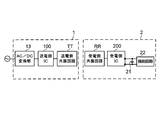
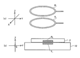
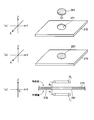
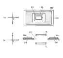
- FIG. 1A and 1B are schematic external views of a power supply device 1 and an electronic device 2 according to the first embodiment of the present invention.
- FIG. 1A is an external view of the power supply device 1 and the electronic device 2 when they are in a separated state
- FIG. 1B is a state where the power supply device 1 and the electronic device 2 are in a reference arrangement state. It is the external view of those times. The significance of the separation state and the reference arrangement state will be described in detail later.
- a contactless power supply system is formed by the power supply device 1 and the electronic device 2.
- the power supply device 1 includes a power plug 11 for receiving commercial AC power and a power supply base 12 formed of a resin material.
- FIG. 2 shows a schematic internal configuration diagram of the power supply device 1 and the electronic device 2.
- the power supply device 1 generates an AC / DC conversion unit 13 that generates and outputs a DC voltage having a predetermined voltage value from a commercial AC voltage input via the power plug 11, and outputs the output voltage of the AC / DC conversion unit 13.
- a power transmission side IC 100 (hereinafter also referred to as IC 100), which is an integrated circuit that is used and driven, and a power transmission side resonance circuit TT (hereinafter also referred to as resonance circuit TT) connected to the IC 100 are provided.
- the AC / DC conversion unit 13, the power transmission side IC 100, and the resonance circuit TT can be arranged in the power supply base 12.
- a circuit that is driven using the output voltage of the AC / DC conversion unit 13 may be provided in the power supply device 1 in addition to the IC 100.
- the electronic device 2 includes a power receiving side IC 200 that is an integrated circuit (hereinafter also referred to as IC 200), a power receiving side resonance circuit RR that is connected to the IC 200 (hereinafter also referred to as resonant circuit RR), and a battery 21 that is a secondary battery. And a functional circuit 22 that is driven based on the output voltage of the battery 21.
- the IC 200 can supply charging power to the battery 21.
- the IC 200 may be driven by the output voltage of the battery 21 or may be driven based on a voltage from a voltage source other than the battery 21.
- a DC voltage obtained by rectifying a signal for NFC communication (details will be described later) received from the power supply device 1 may be the driving voltage of the IC 200.
- the IC 200 can be driven even if the remaining capacity of the battery 21 runs out.
- the electronic device 2 may be any electronic device, such as a mobile phone (including a mobile phone classified as a smart phone), a portable information terminal, a tablet personal computer, a digital camera, an MP3 player, a pedometer, or , A Bluetooth® headset.
- the functional circuit 22 realizes an arbitrary function that the electronic device 2 should realize. Therefore, for example, if the electronic device 2 is a smart phone, the functional circuit 22 transmits / receives information to / from other devices via a call processing unit for realizing a call with the counterpart device and a network. Including a communication processing unit.
- the functional circuit 22 includes a drive circuit that drives the image sensor, an image processing circuit that generates image data from an output signal of the image sensor, and the like.
- the functional circuit 22 may be considered as a circuit provided in an external device of the electronic device 2.
- the resonant circuit TT includes a capacitor T C is a coil T L and the power transmitting side capacitor as the power transmission coil, the resonant circuit RR is the power-receiving-side capacitor and the coil R L is a receiver coil And a capacitor RC .
- the power transmission coil T L and a resonant circuit TT by the power transmission side capacitor T C are connected in parallel to each other are formed as a parallel resonance circuit, and the power receiving side coil It is assumed that the resonance circuit RR is formed as a parallel resonance circuit by connecting R L and the power receiving side capacitor RC in parallel.
- the resonant circuit TT by transmitting coil T L and the power-transmitting-side capacitor T C is connected in series with each other may be formed as a series resonant circuit
- the power receiving side coil R L and the power-receiving-side capacitor R C each other The resonance circuit RR may be formed as a series resonance circuit by being connected in series.
- NFC communication Near field communication wireless communication
- the frequency of the communication carrier is 13.56 MHz (megahertz).
- 13.56 MHz is referred to as a reference frequency. Since NFC communication between the devices 1 and 2 is performed by a magnetic field resonance method using the resonance circuits TT and RR, the resonance frequencies of the resonance circuits TT and RR are both set to the reference frequency. However, as will be described later, the resonance frequency of the resonance circuit RR can be temporarily changed from the reference frequency.
- the power transmission and power reception between the devices 1 and 2 are power transmission by NFC from the power supply device 1 to the electronic device 2 and power reception by NFC in the electronic device 2.
- This power transmission and power reception are collectively referred to as NFC power transmission or simply power transmission.
- NFC power transmission By transmitting the power from the coil T L with respect to the coil R L by magnetic field resonance method, the power transmission is achieved in a non-contact manner.
- the electronic device 2 is placed in a predetermined power transmission area on the power supply stand 12 (the power supply device 1 and the electronic device 2 are in a predetermined positional relationship), in other words, the electronic device 2 is within a predetermined range on the power supply stand 12.
- a state in which the NFC communication and power transmission described above can be realized is referred to as a reference arrangement state (see FIG. 1B).
- a reference arrangement state see FIG. 1B.
- a state in which the electronic device 2 is sufficiently separated from the power supply stand 12 and cannot realize the above-described NFC communication and power transmission is referred to as a separated state (see FIG. 1A).
- the surface of the power supply base 12 shown in FIG. 1A is flat, a depression or the like that matches the shape of the electronic device 2 to be placed may be formed in the power supply base 12.
- the reference arrangement state is a state in which the electronic device 2 exists in a predetermined power transmission region (in other words, a region for performing power transmission and power reception) in which power can be transmitted and received between the power supply device 1 and the electronic device 2.
- the belonging and separated state may be understood as belonging to a state in which the electronic device 2 does not exist in the power transmission area.
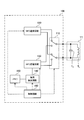
- FIG. 4 shows a partial configuration diagram of the power supply device 1 including an internal block diagram of the IC 100.
- the IC 100 is provided with each part referred to by reference numerals 110, 120, 130, 140, 150 and 160.
- FIG. 5 shows a configuration diagram of a part of the electronic device 2 including an internal block diagram of the IC 200.
- the IC 200 is provided with each part referred to by reference numerals 210, 220, 230, 240 and 250.
- the capacitor 23 that outputs the driving voltage of the IC 200 may be connected to the IC 200.
- the capacitor 23 can output a DC voltage obtained by rectifying a signal for NFC communication received from the power supply device 1.
- the switching circuit 110 connects either the NFC communication circuit 120 or the NFC power transmission circuit 130 to the resonance circuit TT under the control of the control circuit 160.
- the switching circuit 110 can be configured by a plurality of switches interposed between the resonance circuit TT and the circuits 120 and 130. Any switch described herein may be formed using a semiconductor switching element such as a field effect transistor.
- the switching circuit 210 connects the resonance circuit RR to either the NFC communication circuit 220 or the NFC power receiving circuit 230 under the control of the control circuit 250.
- the switching circuit 210 can be configured by a plurality of switches interposed between the resonance circuit RR and the circuits 220 and 230.
- the state where the resonance circuit TT is connected to the NFC communication circuit 120 via the switching circuit 110 and the resonance circuit RR is connected to the NFC communication circuit 220 via the switching circuit 210 is called a communication connection state.
- NFC communication is possible in the communication connection state.
- the NFC communication circuit 120 can supply an AC signal (AC voltage) having a reference frequency to the resonance circuit TT.
- NFC communication between the devices 1 and 2 is performed in a half-duplex manner.
- NFC communication circuit 220 may transmit any information signal (response signal) from the coil R L of the resonance circuit RR to the coil T L of the resonance circuit TT.
- this transmission is based on the ISO standard (for example, ISO 14443 standard), and is based on a load modulation method that changes the impedance of the coil R L (electronic device side antenna coil) viewed from the coil T L (power supply device side antenna coil). Realized.
- the information signal transmitted from the electronic device 2 is extracted by the NFC communication circuit 120.
- the state where the resonance circuit TT is connected to the NFC power transmission circuit 130 via the switching circuit 110 and the resonance circuit RR is connected to the NFC power reception circuit 230 via the switching circuit 210 is referred to as a power supply connection state.
- the NFC power transmission circuit 130 can perform a power transmission operation, and the NFC power reception circuit 230 can perform a power reception operation.
- Power transmission is realized by power transmission operation and power reception operation.
- the power transmission circuit 130 supplies a power transmission magnetic field (power transmission alternating magnetic field) to the power transmission side coil TL by supplying a power transmission AC signal (power transmission AC voltage) to the resonance circuit TT.
- a power transmission AC signal power transmission AC voltage
- electric power is transmitted from the resonance circuit TT (power transmission side coil T L ) to the resonance circuit RR by the magnetic field resonance method.
- the power received by the power receiving coil RL based on the power transmission operation is sent to the power receiving circuit 230.
- the power receiving circuit 230 In the power receiving operation, the power receiving circuit 230 generates and outputs arbitrary DC power from the received power.
- the battery 21 can be charged with the output power of the power receiving circuit 230.
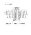
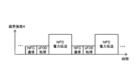
- the magnetic field strength in the NFC communication is within a predetermined range.
- the lower limit value and the upper limit value of the range are determined by NFC standards, and are 1.5 A / m and 7.5 A / m, respectively.
- the strength of the magnetic field generated in the power transmission coil TL (magnetic field strength of the power transmission magnetic field) in power transmission is larger than the above upper limit, for example, about 45 to 60 A / m. .
- NFC communication and power transmission can be performed alternately, and the state of the magnetic field strength at that time is shown in FIG.
- FIG. 7 shows a relationship among the power transmission circuit 130, the load detection circuit 140, and the resonance circuit TT in the power supply connection state. In FIG. 7, the switching circuit 110 is not shown.
- the power transmission circuit 130 amplifies the sine wave signal generated by the signal generator 131 and the signal generator 131 that generates a sine wave signal of a reference frequency, and the amplified sine wave signal is lined with the potential of the line 134 as a reference.
- An amplifier (power amplifier) 132 that outputs between 134 and 135 and a capacitor 133 are provided.
- the load detection circuit 140 includes a sense resistor 141, an envelope detector 142, an amplifier 143, and an A / D converter 144.
- the signal intensity of the sine wave signal generated by the signal generator 131 is fixed to a constant value, but the amplification factor of the amplifier 132 is variably set by the control circuit 160.
- One end of the capacitor 133 is connected to the line 135.
- the other end of the capacitor 133 are connected in common to one ends of the capacitor T C and coil T L, and the coil T L at the other end another line 134 and the capacitor T C via the sense resistor 141 Commonly connected to the ends.
- the power transmission operation is realized by supplying an AC signal (AC voltage for power transmission) from the amplifier 132 to the resonance circuit TT via the capacitor 133.
- an AC signal from the amplifier 132 is supplied to the resonance circuit TT in the power supply connection state, an AC current having a reference frequency flows in the power transmission side coil TL .
- an AC voltage drop occurs in the sense resistor 141.
- a solid line waveform in FIG. 8 is a voltage waveform of a voltage drop in the sense resistor 141.
- the envelope detector 142 outputs an analog voltage signal proportional to the voltage v in FIG. 8 by detecting the envelope of the voltage drop signal in the sense resistor 141.
- the amplifier 143 amplifies and outputs the output signal of the envelope detector 142.
- the A / D converter 144 outputs a digital voltage value V D by converting the output voltage signal of the amplifier 143 into a digital signal.
- the voltage value V D has a value proportional to the amplitude of the current flowing through the sense resistor 141 (and hence the amplitude of the current flowing through the power transmission side coil TL ) (increase in the amplitude). Along with this, the voltage value V D also increases).
- the load detection circuit 140 is a current amplitude detection circuit that detects the amplitude of the current flowing through the power transmission side coil TL , and it can be considered that the amplitude detection value is the voltage value V D.
- the envelope detector 142 may be provided after the amplifier 143. However, as shown in FIG. 7, it is advantageous to provide the envelope detector 142 in front of the amplifier 143 because it is possible to adopt the amplifier 143 having a lower response performance to a high frequency.
- the load detection circuit 140 detects the magnitude of the load by the output voltage value V D, and can be considered.
- the magnitude of the load here can be said to be the magnitude of the load on the power transmission side coil TL at the time of power transmission, and can also be said to be the magnitude of the load of the electronic device 2 as viewed from the power feeding device 1 at the time of power transmission.
- the sense resistor 141 may be provided inside the IC 100 or may be provided outside the IC 100.
- the memory 150 (see FIG. 4) is composed of a nonvolatile memory, and stores arbitrary information in a nonvolatile manner.
- the control circuit 160 comprehensively controls the operation of each part in the IC 100.
- the control performed by the control circuit 160 includes, for example, control of switching operation of the switching circuit 110, content control and execution presence / absence control of communication operation and power transmission operation by the communication circuit 120 and power transmission circuit 130, operation control of the load detection circuit 140, memory 150 storage controls and read controls are included.
- the control circuit 160 has a built-in timer (not shown) and can measure the time length between arbitrary timings.
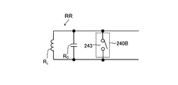
- the electronic device 2 resonance state changing circuit 240 in (see FIG. 5), the resonance frequency change circuit for changing the reference frequency the resonance frequency of the resonance circuit RR to another predetermined frequency f M, or, the power receiving side coil R in the resonance circuit RR This is a coil short circuit for short-circuiting L.
- a resonance frequency changing circuit 240 ⁇ / b> A in FIG. 9 is an example of a resonance frequency changing circuit as the resonance state changing circuit 240.
- the resonance frequency changing circuit 240A includes a series circuit of a capacitor 241 and a switch 242, and one end of the series circuit is commonly connected to one end of each of the capacitor RC and the coil RL , while the other end of the series circuit is the capacitor R. C and the other end of the coil RL are commonly connected.
- the switch 242 is turned on or off under the control of the control circuit 250.
- the resonance circuit RR is formed by only the coil RL and the capacitor RC if the parasitic inductance and the parasitic capacitance are ignored.
- the resonance frequency of the resonance circuit RR matches the reference frequency. That is, when the switch 242 is off, the power receiving side capacitance that determines the resonance frequency of the resonance circuit RR is the capacitor RC itself. Since the capacitor 241 is connected in parallel to the capacitor RC when the switch 242 is on, the resonance circuit RR is formed by the coil RL and the combined capacitance of the capacitors RC and 241. As a result, the resonance circuit RR resonance frequency is low frequency f M than the reference frequency.
- the power receiving side capacitance that determines the resonance frequency of the resonance circuit RR is the above-described combined capacitance.
- the frequency f M is such that the resonance circuit RR does not function as a load on the power transmission side coil TL (ie, enough magnetic resonance does not occur between the resonance circuits TT and RR). It is assumed that it is far from the reference frequency.
- the resonance frequency (that is, the frequency f M ) of the resonance circuit RR when the switch 242 is on is several hundred kHz to 1 MHz.
- the resonance frequency change circuit as changing circuit 240 is not limited to the resonance frequency change circuit 240A, the frequency f M may be higher than the reference frequency.
- the circuit switching the unconnected When the connection is not established, the resonance frequency (>> reference frequency) of the resonance circuit RR is determined by the coil RL and the parasitic capacitance of the wiring).
- the power receiving side resonance circuit RR can be a series resonance circuit.
- the power reception side resonance circuit RR has a parallel circuit or series circuit of a power reception side coil (R L ) and a power reception side capacitance, and the resonance frequency of the power reception side resonance circuit RR when the power reception side capacitance matches a predetermined reference capacitance. f O matches the reference frequency.
- the resonance frequency changing circuit increases or decreases the power receiving side capacitance from the reference capacitance at a necessary timing.
- a parallel circuit or a series circuit is formed by the power receiving side coil (R L ) and the power receiving side capacitance larger or smaller than the reference capacity, and as a result, the resonance frequency of the power receiving side resonance circuit RR.
- f O is changed from the reference frequency.
- a coil short circuit 240B in FIG. 10 is an example of a coil short circuit as the resonance state changing circuit 240.
- the coil short circuit 240B a node where one end of the capacitor RC and one end of the coil RL in the resonance circuit RR are commonly connected, and the other end of the capacitor RC and the other end of the coil RL in the resonance circuit RR are commonly connected.
- the switch 243 is connected (inserted) between the nodes.
- the switch 243 is turned on or off under the control of the control circuit 250. When the switch 243 is turned on, the coil RL in the resonance circuit RR is short-circuited (more specifically, both ends of the coil RL are short-circuited).
- the power receiving side resonance circuit RR does not exist (a state equivalent to a state where the power receiving side resonance circuit RR does not exist). Therefore, while the power receiving coil RL is short-circuited, the load on the power transmitting coil TL is sufficiently lightened (that is, as if the electronic device 2 does not exist on the power supply base 12). As long as the power receiving coil RL can be short-circuited, the coil short-circuit as the changing circuit 240 is not limited to the coil short-circuit 240B.
- the operation of changing the resonance frequency f O of the power reception side resonance circuit RR from the reference frequency in a predetermined frequency f M is called the resonant frequency changing operation, the operation of short-circuit power receiving coil R L by using a coil short circuit This is called a coil short-circuit operation.
- the resonance frequency changing operation or the coil short-circuiting operation may be referred to as f O changing / short-circuiting operation.
- the control circuit 250 comprehensively controls the operation of each part in the IC 200.
- the control performed by the control circuit 250 includes, for example, control of switching operation of the switching circuit 210, content control and execution presence / absence control of communication operation and power reception operation by the communication circuit 220 and power reception circuit 230, and operation control of the change circuit 240. .
- the control circuit 250 has a built-in timer (not shown) and can measure the time length between arbitrary timings. For example, a timer in the control circuit 250, f O changes / short operation due to the resonance frequency f O of the change or the power receiving side time measuring the short-circuit of the coil R L is maintained to a predetermined frequency f M (i.e. below the time T M Measurement; see step S207 in FIG. 19).
- the control circuit 160 of the power supply device 1 can determine whether or not there is a foreign object on the power supply stand 12 and can control the power transmission circuit 130 to perform a power transmission operation only when there is no foreign object.
- the foreign matter in the present embodiment has a current (based on the magnetic field generated by the power transmitting side coil TL when approaching the power feeding device 1. This includes objects that can generate a current in a foreign object.
- the presence of foreign matter may be understood to mean that the foreign matter is present at a position where a non-negligible current flows in the foreign matter based on the magnetic field generated by the power transmission coil TL. .
- the current that has flowed in the foreign matter based on the magnetic field generated by the power transmission side coil TL generates an electromotive force (or counter electromotive force) in the coil ( TL or RL ) that faces and couples to the foreign matter. This can have a non-negligible effect on the characteristics of the circuit including the coil.
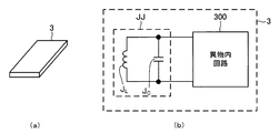
- FIG. 11A shows a schematic external view of a foreign material 3 which is a kind of foreign material
- FIG. 11B shows a schematic internal configuration diagram of the foreign material 3.
- the foreign object 3 includes a resonance circuit JJ composed of a parallel circuit of a coil J L and a capacitor J C , and a foreign substance circuit 300 connected to the resonance circuit JJ.
- the resonance frequency of the resonance circuit JJ is set to the reference frequency.
- the foreign material 3 is a device that does not correspond to the power supply device 1.
- the foreign material 3 is an object (such as a non-contact IC card) having a wireless IC tag having an antenna coil (coil J L ) of 13.56 MHz that does not respond to NFC communication.
- the foreign object 3 is an electronic device that has the NFC communication function itself but is disabled.
- a smartphone that has an NFC communication function but whose function is turned off by software setting can be a foreign object 3.
- a smart phone in which the NFC communication function is valid a smart phone that does not have a power receiving function is classified as the foreign object 3.
- a strong magnetic field for example, a magnetic field strength of 12 A / m or more generated by the power transmission side coil TL is generated.
- the foreign matter 3 may be destroyed by the magnetic field having For example, a strong magnetic field during the transmission operation, also have to increase the terminal voltage of the coil J L foreign material 3 on the feeding table 12 up to 100 V ⁇ 200V, foreign body 3 is formed to withstand such a high voltage If not, the foreign material 3 is destroyed.
- FIG. 12 is a flowchart of foreign object detection processing (hereinafter referred to as pFOD processing) executed by the power supply device 1 before power transmission.
- the control circuit 160 When executing the pFOD process, the power transmission circuit 130 is connected to the resonance circuit TT.
- the control circuit 160 first sets the magnetic field strength H by the power transmission side coil TL to a predetermined test strength in step S11.
- the magnetic field strength H is a magnetic field strength generated by the power transmission side coil TL , and more specifically indicates a magnetic field strength of an alternating magnetic field that vibrates at a reference frequency generated by the power transmission side coil TL . Setting the magnetic field strength H to the test strength means that the power transmission circuit 130 is controlled so that a predetermined test AC signal (test AC voltage) is supplied to the resonance circuit TT, thereby having the test strength and the reference frequency.
- the control circuit 160 can variably set the magnetic field strength H by controlling the amplification factor of the amplifier 132 (see FIG. 7).
- a predetermined test AC voltage is supplied to and applied to the resonance circuit TT when the test magnetic field is generated, and a predetermined amplitude having a larger amplitude than the test AC voltage is generated when the power transmission magnetic field is generated.
- the amplification factor of the amplifier 132 may be controlled so that the AC voltage for power transmission is supplied and applied to the resonance circuit TT.
- step S12 the control circuit 160 uses the load detection circuit 140 to acquire the voltage value V D when the test magnetic field is generated as the current amplitude detection value V pFOD .
- Current amplitude detection value V PFOD has a value corresponding to the amplitude of the current flowing through the power transmitting coil T L when to generate a test magnetic field to the power transmission coil T L.
- f O changes / short operation in the electronic apparatus 2 in accordance with an instruction from the power supply apparatus 1 via the NFC communication (resonance frequency change operation or coil short circuit operation) is being performed . Therefore, the resonance circuit RR (power reception side coil R L ) does not substantially function as a load of the power transmission side coil T L and causes no or almost no decrease in the current amplitude detection value V pFOD .
- step S13 the control circuit 160 determines whether or not the current amplitude detection value V pFOD is within a predetermined pFOD normal range.
- the control circuit 160 determines that the foreign material 3 does not exist on the power supply base 12 (step S14). This determination is referred to as foreign object determination.
- the control circuit 160 determines that the foreign material 3 exists on the power supply base 12 (step S15). This determination is referred to as a foreign object determination.
- the control circuit 160 determines that the power transmission operation by the power transmission circuit 130 is possible, permits the power transmission operation (power transmission using the resonance circuit TT), and determines whether there is a foreign object. If it has been established, it is determined that the power transmission operation by the power transmission circuit 130 is impossible, and the execution of the power transmission operation is prohibited. When it is determined that the power transmission operation can be performed, in the power transmission operation, the control circuit 160 can control the power transmission circuit 130 such that a predetermined power transmission magnetic field is generated in the power transmission side coil TL .
- the pFOD normal range is a range that is not less than a predetermined lower limit value V pREFL and not more than a predetermined upper limit value V pREFH (0 ⁇ V pREFL ⁇ V pREFH ). Therefore, when the determination inequality “V pREFL ⁇ V pFOD ⁇ V pREFH ” is satisfied, the foreign object determination is made, and otherwise, the foreign object determination is made.
- the resonance circuit JJ (coil J L ) of the foreign matter 3 functions as a load of the power transmission side coil TL.
- the current amplitude detection value V pFOD is decreased as compared with the case where no foreign matter 3 exists in FIG.
- the foreign material 3a (not shown) different from the foreign material 3 is also considered as a foreign material.
- the foreign material 3a is, for example, a metal body (aluminum foil or aluminum plate) formed including aluminum or a metal body formed including copper.
- the current amplitude detection value V pFOD is less than the lower limit value V pREFL , and the foreign object 3a is present on the power supply table 12. If the current amplitude detection value V pFOD exceeds the upper limit value V pREFH and no foreign matter (3 or 3a) is present on the power supply base 12, the current amplitude detection value V pFOD is pFOD.
- the lower limit value V pREFL and the upper limit value V pREFH are set in advance and stored in the memory 150 through experiments or the like so as to be within the normal range.
- the magnetic field for power transmission is generated in a state where the foreign object 3a exists on the power supply stand 12, the power is absorbed by the foreign object 3a, and the foreign object 3a may generate heat.
- the reference frequency as the carrier frequency of power transmission is 13.56 MHz, it can be said that the possibility of such heat generation is sufficiently small. Therefore, the presence of foreign matter is determined only when the current amplitude detection value V pFOD falls below the lower limit value V pREFL without considering the presence of the foreign matter 3a, and the current amplitude detection value V pFOD is greater than or equal to the lower limit value V pREFL.
- the foreign object non- existence determination may be performed (that is, the upper limit value V pREFH may be eliminated).
- the reference frequency in the invention according to the present embodiment is not limited to 13.56 MHz, in the case where the reference frequency, for example, about several 100kHz, because fear of heat generation of the foreign matter 3a is higher, only the lower limit value V PREFL It is desirable to adopt the above-described method in which the upper limit value V pREFH is set to the normal range of pFOD.
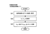
- FIG. 13 is an operation flowchart of the initial setting process.
- the initial setting process is executed by the IC 100 under the following initial setting environment.
- the initial setting process may be performed at the time of manufacturing or shipping the power supply device 1. However, if the initial setting environment can be secured, the initial setting process can be performed at an arbitrary timing.
- the power transmission circuit 130 When executing the initial setting process, the power transmission circuit 130 is connected to the resonance circuit TT. Then, in step S21, the magnetic field strength H by the power transmission side coil TL is set to a predetermined test strength, and in the subsequent step S22, the voltage value V D acquired from the A / D converter 144 in the set state is set as the voltage. Obtained as the value V DO . In subsequent step S23, lower limit value V pREFL based on voltage value V DO is stored in memory 150. The lower limit value V pREFL is set to a value lower than the voltage value V DO so that the presence of foreign matter is determined in the pFOD process only in the presence of the foreign matter 3.
- k is a coefficient having a positive predetermined value less than 1. Note that the voltage value V D that would be obtained when the magnetic field strength H is set to a predetermined test strength in the initial setting environment can be estimated at the design stage. Based on the value derived by this estimation, the lower limit value V pREFL may be determined and stored in the memory 150 without performing the initial setting process.
- the load on the power transmission side coil T L is sufficiently lightly (That is, it is as if the electronic device 2 does not exist on the power supply stand 12), and the current amplitude detection value V pFOD becomes sufficiently large to determine that there is no foreign object.
- the resonance frequency of the resonance circuit RR is changed to the frequency f M or the power reception side coil RL is short-circuited, the foreign matter 3 continues to exist as a load of the power transmission side coil TL. For this reason (because the resonance frequency of the resonance circuit JJ of the foreign material 3 remains the reference frequency), the current amplitude detection value V pFOD becomes sufficiently small and foreign matter determination is made.
- the power supply device 1 can determine whether or not the electronic device 2 that can support power transmission exists on the power supply base 12 by NFC communication.
- the state in which the foreign object 3 is present on the power supply base 12 is not limited to the state in which the foreign object 3 is in direct contact with the power supply base 12. For example, as shown in FIG. 15, a foreign object presence determination is also made in a state where the electronic device 2 exists in direct contact with the power supply stand 12 and the foreign material 3 exists on the electronic device 2. As long as the foreign object 3 exists on the power supply stand 12, it belongs.
- the power supply device 1 is a transmission side and the electronic device 2 is a reception side, and the power supply device 1 (IC 100) transmits an inquiry signal 510 to a device on the power supply base 2 (hereinafter also referred to as a power supply target device) by NFC communication.
- the power supply target device includes the electronic device 2 and may include the foreign material 3.
- the inquiry signal 510 is, for example, a signal for inquiring unique identification information of a power supply target device, a signal for inquiring whether the power supply target device is in a state where NFC communication can be performed, and whether the power supply target device can receive power or transmit power. It includes a signal that asks if you are seeking
- the electronic device 2 (IC 200) that has received the inquiry signal 510 transmits a response signal 520 that answers the inquiry content of the inquiry signal 510 to the power supply device 1 by NFC communication.
- the power supply device 1 (IC 100) that has received the response signal 520 analyzes the response signal 520, and if the power supply target device is capable of NFC communication and can receive power or requests power transmission, a test request
- the signal 530 is transmitted to the power supply target device by NFC communication.
- the electronic device 2 (IC 200) as the power supply target device that has received the test request signal 530 transmits a response signal 540 to the test request signal 530 to the power supply device 1 by NFC communication, and then promptly changes the f O / A short-circuit operation (resonance frequency changing operation or coil short-circuit operation) is executed.
- the test request signal 530 is a signal for requesting and instructing execution of the f O change / short circuit operation
- the control circuit 250 of the electronic device 2 receives the test request signal 530 as an opportunity to change / short circuit the f O.
- the operation is executed by the resonance state changing circuit 240.
- the f O change / short-circuit operation is not executed.
- f O changes / short test request signal 530 if the trigger for the execution of the operation may be any signal, or may be contained in the inquiry signal 510.
- the power supply apparatus 1 (IC 100) that has received the response signal 540 executes the above-described pFOD process.
- the electronic device 2 (IC 200) continues to execute the f 2 O change / short-circuit operation.
- the electronic device 2 (IC 200) is built-in timer with, f O changes / short since maintaining the execution of only f O changes / short operation time corresponding to the length of the execution period of pFOD process Stop operation.
- the power supply device 1 transmits an authentication signal 550 to the power supply target device by NFC communication.
- the authentication signal 550 includes, for example, a signal for notifying the power supply target device that power transmission will be performed from now on.
- the electronic device 2 (IC 200) that has received the authentication signal 550 transmits a response signal 560 corresponding to the authentication signal 550 to the power supply device 1 by NFC communication.
- the response signal 560 includes, for example, a signal notifying that the content indicated by the authentication signal 550 has been recognized or a signal giving permission to the content indicated by the authentication signal 550.
- the power supply device 1 (IC 100) that has received the response signal 560 executes the power transmission operation by connecting the power transmission circuit 130 to the resonance circuit TT, thereby realizing the power transmission 570.
- the power transmission 570 is executed according to the above flow. However, in the second case of FIG. 14B, the process proceeds until the transmission / reception of the response signal 540. Since it is determined that there is a foreign object on the power supply stand 12 in the pFOD process, the power transmission 570 is not executed.
- One power transmission 570 may be performed only for a predetermined time, and a series of processing from transmission of the inquiry signal 510 to power transmission 570 may be repeatedly executed.
- NFC communication, pFOD processing, and power transmission NFC power transmission
- NFC power transmission can be executed sequentially and repeatedly. That is, in the non-contact power supply system, the operation of performing NFC communication, the operation of performing pFOD processing, and the operation of performing power transmission (NFC power transmission) can be repeatedly performed in order in a time division manner.
- FIG. 18 is an operation flowchart of the power supply device 1. The operations of the communication circuit 120 and the power transmission circuit 130 are executed under the control of the control circuit 160.
- step S101 the control circuit 160 connects the communication circuit 120 to the resonance circuit TT through the control of the switching circuit 110.
- the control circuit 160 transmits an inquiry signal 510 to the power supply target device by NFC communication using the communication circuit 120 and the resonance circuit TT, and then waits for reception of the response signal 520 in step S103.
- the control circuit 160 analyzes the response signal 520, and the power supply target device is capable of NFC communication and can receive power or request power transmission.
- step S104 Y in step S104
- the process proceeds to step S105. Otherwise (N in step S104), the process returns to step S102.
- step S105 the control circuit 160 transmits the test request signal 530 to the power supply target device by NFC communication using the communication circuit 120 and the resonance circuit TT, and then waits for reception of the response signal 540 in step S106.
- the control circuit 160 connects the power transmission circuit 130 to the resonance circuit TT through the control of the switching circuit 110, and in the subsequent step S108, the above-described pFOD process is performed. Do.
- step S109 the control circuit 160 connects the communication circuit 120 to the resonance circuit TT through the control of the switching circuit 110, and proceeds to step S110.
- step S108 if foreign matter determination is made, the process returns from step S110 to step S102, but if foreign matter non-judgment is made, the process proceeds from step S110 to step S111.
- step S111 the control circuit 160 transmits the authentication signal 550 to the power supply target device by NFC communication using the communication circuit 120 and the resonance circuit TT, and then waits for reception of the response signal 560 in step S112.
- step S113 the control circuit 160 connects the power transmission circuit 130 to the resonance circuit TT through the control of the switching circuit 110, and proceeds to step S114.
- the control circuit 160 sets the power transmission permission flag to ON in step S114, starts the power transmission operation and the mFOD process, and then proceeds to step S115.
- step S115 the presence or absence of a foreign object during power transmission is detected by the mFOD process, and when a foreign object is detected, the power transmission permission flag is turned off.
- the control circuit 160 measures the elapsed time from the start time of the power transmission operation, and compares the elapsed time with a predetermined time t A (for example, 10 minutes) and checks the state of the power transmission permission flag in step S115. When the elapsed time reaches a predetermined time t A or when the power transmission permission flag is set to OFF by the mFOD process, the process proceeds to step S116.
- step S116 the control circuit 160 switches the power transmission permission flag from ON to OFF or maintains the power transmission permission flag OFF, stops the power transmission operation and the mFOD process, and then returns to step S101.
- FIG. 19 is an operation flowchart of the electronic device 2, and the process starting from step S201 is executed in conjunction with the operation of the power supply device 1 shown in FIG.
- the operations of the communication circuit 220 and the power receiving circuit 230 are executed under the control of the control circuit 250.
- step S201 the control circuit 250 connects the communication circuit 220 to the resonance circuit RR through the control of the switching circuit 210.
- the f O change / short-circuit operation is not executed when the electronic device 2 is activated.
- step S202 control circuit 250 uses communication circuit 220 and waits for reception of inquiry signal 510.
- step S203 the control circuit 250 analyzes the inquiry signal 510 to generate a response signal 520, and generates the response signal 520 by NFC communication using the communication circuit 220. Transmit to the power supply device 1.
- the control circuit 250 confirms the state of the battery 21, and if the battery 21 is not fully charged and no abnormality is recognized in the battery 21, a signal for receiving power or requesting power transmission is sent to the response signal 520. include. On the other hand, if battery 21 is fully charged or if abnormality is recognized in battery 21, a signal indicating that power cannot be received is included in response signal 520.
- step S205 the control circuit 250 transmits a response signal 540 to the feeding apparatus 1 by the NFC communication using the communication circuit 220, perform a f O changes / short operation using a resonance state changing circuit 240 at the subsequent step S206 To do. That is, short-circuiting or the power receiving coil R L changes from the reference frequency of the resonance frequency f O to the frequency f M.
- the control circuit 250 measures the time elapsed from the start of the f O changes / short operation (step S207), and stops the f O changes / short operation when the elapsed time reaches the predetermined time t M ( Step S208).
- the resonance frequency f O is returned to the reference frequency or the short circuit of the power receiving coil RL is eliminated. Thereafter, the process proceeds to step S209.
- f O changes / short run operations is maintained, promptly f O changes / short the end of that time operation time t M as stopped is preset.
- the time t M may be specified in the test request signal 530.
- step S209 the control circuit 250 waits for reception of the authentication signal 550 using the communication circuit 220.
- the control circuit 250 transmits a response signal 560 to the authentication signal 550 to the power supply device 1 by NFC communication using the communication circuit 220 in step S 210. If a foreign object exists on the power supply stand 12, the authentication signal 550 is not transmitted from the power supply device 1 (see step S110 in FIG. 18). Therefore, if the authentication signal 550 is not received for a predetermined time in step S209. It is good to return to step S201.
- step S211 the control circuit 250 connects the power reception circuit 230 to the resonance circuit RR through the control of the switching circuit 210, and starts a power reception operation using the power reception circuit 230 in step S212.
- the control circuit 250 measures the time elapsed from the start of the power receiving operation, and compares the elapsed time with a predetermined time t B (step S213). Then, the elapsed time reaches the time t B (Y in step S213), in step S214, the control circuit 250, a power receiving operation is stopped and the flow returns to step S201.
- the time t B is predetermined or specified in the authentication signal 550 so that the period during which the power receiving operation is performed substantially coincides with the period during which the power transmission operation is performed in the power supply device 1. .
- the control circuit 250 monitors the charging current to the battery 21 and determines that the power transmission operation is terminated when the charging current value becomes equal to or lower than the predetermined value. You may make it perform transfer to.
- a foreign object may be placed on the power supply stand 12 after the power transmission operation is started.
- the mFOD process functions as a foreign object detection process during power transmission, and the presence or absence of a foreign object is continuously monitored during power transmission by the mFOD process.
- FIG. 20 is an operation flowchart of the mFOD process.
- the control circuit 160 repeatedly executes the mFOD process in FIG. 20 during the period during which the power transmission operation is performed.
- the control circuit 160 first acquires the latest voltage value V D as the current amplitude detection value V MFOD step S51.
- Current amplitude detection value V MFOD has a value corresponding to the amplitude of the current flowing through the power transmitting coil T L when is generating power for the magnetic field to the power transmission coil T L.
- the control circuit 160 determines whether or not the current amplitude detection value V mFOD belongs to a predetermined mFOD normal range.
- step S53 If the current amplitude detection value V mFOD belongs to the mFOD normal range, the foreign object non-determination is determined (step S53), the process returns to step S51, and the processing of steps S51 and S52 is repeated, but the current amplitude detection value V mFOD is mFOD.
- the foreign matter presence determination is made in step S54, and the power transmission permission flag is set to OFF.
- the power transmission permission flag is a flag managed by the control circuit 160 and is set to ON or OFF. When the power transmission permission flag is ON, the control circuit 160 permits the execution of the power transmission operation, and when the power transmission permission flag is OFF, the control circuit 160 prohibits the execution of the power transmission operation or stops the power transmission operation.
- the mFOD normal range is a range not less than a predetermined lower limit value V mREFL and not more than a predetermined upper limit value V mREFH (0 ⁇ V mREFL ⁇ V mREFH ). Therefore, when the determination inequality “V mREFL ⁇ V mFOD ⁇ V mREFH ” is satisfied, the foreign object determination is made, and otherwise, the foreign object determination is made.
- the foreign material 3 formed as a non-contact IC card is inserted between the power supply base 12 of the power supply device 1 and the electronic device 2.
- the coil J L of the power receiving coil R L and foreign substances 3 of the electronic device 2 is magnetically coupled, resonant frequency is the reference frequency of the resonant circuit RR of the electronic device 2 together with the resonance frequency of the resonance circuit JJ foreign matter 3 Deviation from (13.56 MHz).
- the power received by the power receiving side coil RL decreases, and the load of power transmission viewed from the power transmitting side coil TL becomes lighter.
- the upper limit value V mREFH may be determined so that “V mREFH ⁇ V mFOD ”.
- a foreign material 3 b as an iron plate or a ferrite sheet is inserted between the power supply base 12 of the power supply device 1 and the electronic device 2.
- a current flows in the foreign matter 3b through the electrical and magnetic action, and as a result, the amplitude of the current flowing in the power transmission side coil TL is reduced (in this case, the lower limit is such that “V mFOD ⁇ V mREFL ”).
- the value V mREFL may be determined).
- the current amplitude detection value V mFOD changes depending on the presence or absence of the foreign matter including the foreign matters 3 and 3b.
- the lower limit value V MREFL and the upper limit value V MREFH may be stored in the memory 150. Further, it is estimated by theoretical calculation how much the current amplitude detection value V mFOD changes due to the presence of a foreign substance during power transmission, and based on the estimation result, the lower limit value V mREFL is not required.
- the upper limit value V mREFH may be determined and stored in the memory 150. At this time, for example, an object that changes the current amplitude detection value V mFOD by a predetermined change rate or more with reference to the center value of the mFOD normal range may be defined as a foreign object.
- the amplification factor of the amplifier 143 shown in FIG. 7 is variable.
- the amplitude of the current flowing through the power transmitting coil T L is than when performing pFOD treatment, is much To larger when performing the power transmission operation and mFOD process. Therefore, the control circuit 160 sets the amplification factor of the amplifier 143 smaller when performing the mFOD process than when performing the pFOD process, thereby setting the input signal range of the A / D converter 144 between the pFOD process and the mFOD process. Same level.
- the envelope detector 142 and the A / D converter 144 may be inserted between the two.
- amplitude information obtained by performing high-frequency reduction processing in other words, averaging processing or low-pass filtering
- V D voltage value
- the high-frequency reduction process is a process for reducing (attenuating) a relatively high frequency signal component while allowing a relatively low frequency signal component in the voltage drop signal of the sense resistor 141 to pass.
- a high-frequency reduction process is performed on the voltage value V D generated by the output signal of the A / D converter 144.
- the voltage value V D after the high-frequency reduction process may be used as the current amplitude detection value V mFOD (the same may be applied to the current amplitude detection value V pFOD in the pFOD process).
- the high frequency reduction processing by calculation is processing executed by the control circuit 160, and passes a relatively low frequency signal component in the output signal of the A / D converter 144, while relatively high frequency signal component. This is a process for reducing (attenuating).
- the role of the mFOD process is not limited only to the presence / absence determination of foreign matter.
- the mFOD process has a role of turning off the power transmission permission flag under any circumstances inappropriate for continuation of the power transmission operation such that the current amplitude detection value V mFOD deviates from the mFOD normal range.
- the power transmission permission flag is turned OFF (step S54 in FIG. 20).
- control circuit 160 controls whether or not the power transmission is continued by monitoring whether or not the current amplitude detection value V mFOD is out of the mFOD normal range when power is being transmitted by the power transmission operation. To do. As a result, since the power transmission operation is stopped through the mFOD process in a situation inappropriate for the continuation of the power transmission operation, such as when a foreign object is placed on the power supply stand 12 after the power transmission operation is started, the foreign material due to the continuation of the power transmission operation is stopped. Can be avoided.
- a power transmission device WA 1 includes a power transmission side resonance circuit including a power transmission side coil (T L ) for transmitting the power in a power transmission device capable of transmitting power to the power reception device by a magnetic field resonance method. (TT), a power transmission circuit (130) capable of supplying an AC voltage to the power transmission side resonance circuit, a detection circuit (140) for detecting an amplitude of a current flowing in the power transmission side coil, and controlling the power transmission circuit And a control circuit (160) for performing power transmission control of the power when the power transmission is performed based on the amplitude detection value ( VmFOD ) of the detection circuit. It is characterized by controlling the continuation of
- a non-contact power feeding system WA 2 includes a power transmission device having a power transmission side resonance circuit (TT) including a power transmission side coil (T L ) for transmitting power, and for receiving the power. And a power receiving device having a power receiving side resonance circuit (RR) including a power receiving side coil (R L ), and capable of transmitting and receiving the power by a magnetic resonance method.
- a power transmission circuit (130) capable of supplying an AC voltage to the side resonance circuit, a detection circuit (140) for detecting an amplitude of a current flowing in the power transmission side coil, and controlling the power transmission by controlling the power transmission circuit.
- the power transmission device WA 1 and the non-contact power feeding system WA 2 it is inappropriate for the continuation of the power transmission operation, for example, when a foreign object is present at the position where the magnetic field generated by the power transmission side coil reaches after the power transmission operation is started. Under circumstances, it is possible to stop the power transmission operation. For example, it is possible to avoid damage to foreign objects due to continued power transmission.
- the control circuit when the power is transmitted, the control circuit has an amplitude detection value of the detection circuit within a predetermined range (mFOD normal range). It is good to control the continuation of the power transmission by monitoring whether or not it deviates.
- the power transmission may be stopped when a deviation of the amplitude detection value of the detection circuit from the predetermined range is detected.
- the control circuit determines whether or not the amplitude detection value of the detection circuit deviates from the predetermined range when the power is transmitted. Therefore, it is preferable to determine whether or not there is a foreign object that is different from the power receiving apparatus and can generate a current based on the magnetic field generated by the power transmission side coil.
- the control circuit detects that the amplitude detection value of the detection circuit exceeds the upper limit value of the predetermined range when the power is transmitted. By determining whether or not there is a foreign object including a coil as the foreign object, it may be determined.
- the power reception device includes a power reception side resonance circuit (RR) including a power reception side coil (R L ) for receiving the power, and the power reception side resonance prior to power reception.
- RR power reception side resonance circuit
- R L power reception side coil
- a change / short circuit (240) for changing the resonance frequency of the circuit from the resonance frequency at the time of power reception or short-circuiting the power reception coil, and the control circuit (160) is based on communication from the power transmission device
- a predetermined test magnetic field is generated in the power transmission side coil prior to the power transmission in a state in which the power reception device changes the resonance frequency of the power reception side resonance circuit or the power reception side coil is short-circuited in accordance with the signal.
- a first processing unit that controls the power transmission circuit determines the possibility of execution of the transmission when said test magnetic field is generated
- the power transmission is realized by controlling the power transmission circuit so that a power transmission magnetic field larger than the test magnetic field is generated in the power transmission side coil after determining that the power transmission can be performed by two processing units (pFOD processing)
- a third processing unit, and the detection circuit (140) detects the amplitude through a process of amplifying a signal indicating the amplitude of the current flowing through the power transmission coil, and the amplification factor in the amplification is It is preferable that the time when the power transmission magnetic field is generated by the power transmission side coil is smaller than when the test magnetic field is generated by the power transmission side coil.
- the power receiving device changes the resonance frequency of the power receiving side resonance circuit from the resonance frequency at the time of power reception or short-circuits the power receiving side coil before receiving the power.
- the control circuit (160) includes a change / short circuit (240), and the control circuit (160) changes the resonance frequency of the power reception side resonance circuit or shorts the power reception side coil in the power reception device according to a signal from the power transmission device.
- a first processing unit that controls the power transmission circuit so that a predetermined test magnetic field is generated in the power transmission side coil prior to the power transmission, and the detection circuit when the test magnetic field is generated.
- the second processing unit that determines the possibility of execution of the transmission and (PFOD process), the test after determining that can execute the transmission based on the amplitude detection value (V pFOD)
- a third processing unit that realizes the power transmission by controlling the power transmission circuit so that a magnetic field for power transmission larger than the field is generated by the coil on the power transmission side, and the detection circuit (140) includes the power transmission
- the amplitude is detected through a process of amplifying a signal indicating the amplitude of the current flowing in the side coil, and the amplification factor in the amplification is higher than that when the test magnetic field is generated in the power transmission side coil. It is better if the power transmission magnetic field is generated by the side coil.
- the second processing unit By providing the second processing unit, it is possible to prevent power transmission under circumstances inappropriate for power transmission, such as when a foreign object exists at a position where the magnetic field generated by the power transmission coil reaches, In addition, it is possible to avoid damage to foreign matters due to the execution (start of execution) of power transmission. Also, by determining the amplification factor as described above, it becomes possible to make the signal level after amplification the same level between when the test magnetic field is generated and when the power transmission magnetic field is generated. It becomes easy to share a circuit for processing the amplified signal.
- the electric power feeder 1 in 1st Embodiment mentioned above may function as a power transmission apparatus which concerns on this invention, or a part of electric power feeder 1 in the above-mentioned 1st Embodiment functions as a power transmission apparatus which concerns on this invention. You may do it.
- the electronic device 2 itself in the first embodiment described above may function as a power receiving device according to the present invention, or a part of the electronic device 2 in the first embodiment described above may serve as the power receiving device according to the present invention. May function.
- Second Embodiment A second embodiment of the present invention will be described.
- the second embodiment is an embodiment based on the first embodiment.
- the description of the first embodiment is applied to the second embodiment as long as there is no contradiction.
- an X axis, a Y axis, and a Z axis that are orthogonal to each other are defined.
- a plane parallel to the X axis and the Y axis, a plane parallel to the Y axis and the Z axis, and a plane parallel to the Z axis and the X axis may be referred to as an XY plane, a YZ plane, and a ZX plane, respectively.
- the X axis and the Y axis are parallel to the mounting surface of the power supply table 12, and therefore the Z axis is orthogonal to the mounting surface of the power supply table 12.
- the mounting surface of the power supply base 12 is a surface on which the electronic device 2 is to be mounted, and the electronic device 2 and a foreign object can be mounted on the mounting surface.
- the electronic device 2 is mounted on the power supply stand 12 in the standard arrangement state. It shall be placed on the surface. In the reference arrangement state, the power supply device 1 and the electronic device 2 are in a predetermined positional relationship for transmitting and receiving power.
- FIG. 23 (a), (b) is a schematic perspective view of the power transmission coil T L and a power receiving side coil R L of the power supply device 1 and the electronic apparatus 2 in the reference arrangement, a cross-sectional view.
- 24A and 24B show the coils T L and J in the power supply device 1 and the foreign material 3 in a state where the foreign material 3 represented by the non-contact IC card is placed on the mounting surface of the power supply table 12.
- 2 is a schematic perspective view and a sectional view of L.
- FIG. 23 (a) and FIG. 24 (a) the windings of the coils T L , R L and J L are represented by double circles for simplification and prevention of complication (illustration to be described later). The same applies to 25 (c) and the like).
- a line segment extending laterally from a double circle representing the coil represents a lead wire of the coil.
- the cross sections in the cross-sectional views of FIGS. 23B and 24B are parallel to the YZ plane.
- Each of the coils T L , R L and J L forms a loop antenna.
- the loop surface of the loop antenna as the coils T L and R L (that is, the surface on which the windings of the coils T L and R L are arranged) is parallel to the XY plane, and thus the coils T L and The central axis of R L is parallel to the Z axis.
- Coil T L is the winding (such as copper) is formed by the wound around the central axis of its own (the same is true for the coil R L and J L). Also, keep state where foreign matter 3 is placed on the mounting surface of the feed table 12, the loop plane of the loop antenna as a coil J L (i.e., the surface coil windings J L is located), the usually parallel to the same XY plane as the coil T L, thus the central axis of the coil J L is parallel to the Z axis.
- the coils T L and R L have the same shape on the XY plane (however, they may have different shapes).
- the shape of the coil is a concept including the size of the coil.
- the size of the coil may be considered to represent the area occupied by the outer periphery of the coil in the direction orthogonal to the central axis of the coil.
- the area of the portion surrounded by the coil winding on the loop surface of the loop antenna (that is, the surface on which the coil winding is disposed) is It corresponds to the size of the coil.
- the outer peripheral shape of the coils T L and RL (in other words, the outer shape) is a circle, but the outer peripheral shape of the coil is a circle in each of the coils T L and RL.
- the shape is not limited, and may be an ellipse or a polygon (such as a rectangle), and a straight line and a curve may be mixed in the outer peripheral shape of the coil.
- the power receiving side metal part MT 2 may constitute all or part of the casing of the electronic device 2. That is, for example, the power receiving side metal part MT 2 may be a box-shaped metal case as a casing of the electronic device 2. Alternatively, for example, the housing of the electronic device 2 and the power-receiving-side metal section MT 2 is formed of a resin material may be fixed in the housing of the electronic device 2. Power-receiving-side metal section MT 2 is mainly example, it is provided to enhance the structural strength and texture of the electronic device 2.
- Metal constituting the power-receiving-side metal section MT 2 is assumed to be aluminum.
- Metal constituting the power-receiving-side metal section MT 2 is an alloy of aluminum and other metals, may be i.e. aluminum alloy (e.g., duralumin serving as an alloy of aluminum and copper).
- aluminum alloy e.g., duralumin serving as an alloy of aluminum and copper.
- the metal constituting the power-receiving-side metal section MT 2 is other than aluminum or aluminum alloy But it ’s okay.
- Power-receiving-side metal section MT 2 is what may shape have, but assumed to have a metal plate 270 such, having an opening 271 as shown in FIG. 25 (a).
- the metal plate 270 is parallel to the XY plane.
- the opening 271 is a hole that is provided in the metal plate 270 and penetrates in the Z-axis direction. Therefore, no metal exists in the opening 271.
- the opening 271 forms a closed region on the XY plane, and there is no contact between the opening 271 and the outer periphery of the metal plate 270. Therefore, an electric circuit (current loop) made of aluminum is formed around the opening 271 in the XY plane.
- the opening 271 can be sealed with a material other than a metal such as a resin material.
- the resin material is, for example, polycarbonate or polypropylene.
- the outer shape of the metal plate 270 is a rectangle on the XY plane.
- the outer shape of the metal plate 270 is not limited to this on the XY plane, and may include a curve, or a straight line and a curve may be mixed in the outer shape of the metal plate 270.
- the shape of the opening 271 on the XY plane is assumed to be a circle (a cylindrical shape when considered in three dimensions).
- the shape of the opening 271 is not limited to a circle on the XY plane, and may be an ellipse or many shapes. It may be a square (rectangular or the like), and a straight line and a curve may be mixed in the shape of the opening 271.
- Power-receiving-side metal section MT 2 in addition to the metal plate 270 may also include other metal parts. That is, for example, as shown in FIG. 26, when the power-receiving-side metal section MT 2 is a box-shaped metal case CS MT2 as a housing of the electronic device 2, the metal plate 270 is one side of the metal case CS MT2 ( Bottom surface).
- FIG. 25A is a perspective view of the metal plate 270 in the reference arrangement state
- FIG. 25B is a transparent view of some components of the power supply device 1 and the electronic device 2 in the reference arrangement state
- FIG. 25C is a plan view of the metal plate 270 and the power reception side coil RL in the reference arrangement state viewed from the Z-axis direction.
- Opening 271 is provided in (a position opposite with respect to the arrangement position of the power receiving coil R L) position opposing the arrangement position of the power receiving coil R L, the reference arrangement, the opening 271 and the coil T L Located between R L , the coils T L and R L face each other through the opening 271.
- the size of the opening 271 is larger than the size of the coils T L and R L , and when the coil R L , the opening 271, and the coil T L are viewed along the Z-axis direction, the coils R overlapping each other.
- the outer peripheries of L and T L are enclosed in the opening 271.
- the shape of the opening 271 and the outer peripheral shapes of the coils R L and T L are all circles, the centers of these circles are located on one straight line parallel to the Z axis, and as shown in FIG.
- the radius r1 of the circle as the shape of the opening 271 is larger than the radius r2 of the circle as the outer peripheral shape of the coils RL and TL .
- the power transmission using the coils T L and R L can be satisfactorily realized with some loss.
- the loss ratio seen from the case without the metal plate 270 is about 10 to 20%.
- the power transmission side coil TL is magnetically coupled to the metal plate 270 having the opening 271.
- an alternating current I 1 flows through the power transmission side coil TL
- an alternating current in the opposite direction ie, 180 degrees out of phase
- the current I 31 flows through the electric circuit around the opening 271 in the metal plate 270.
- the coupling coefficient between the power transmission side coil TL and the metal plate 270 is K 13
- the power receiving coil RL is also magnetically coupled to the metal plate 270 having the opening 271.
- alternating current I 2 flows, whereby on the basis of the magnetic field generated in the receiver coil R L, and the AC current I 2 reverse (shifted ie 180 degrees out of phase) by electromagnetic induction AC
- the current I 32 flows through the electric circuit around the opening 271 in the metal plate 270.
- FIG. 28 (c) shows currents I 1 , I 2 , I 31 and I 32 on a complex plane.
- K 12 is the coupling coefficient between coils T L and R L in the standard arrangement
- Q is Q of the power receiving coil R L
- j is an imaginary.
- the phase of the current I 2 is delayed by 90 degrees with respect to the current I 1 .
- the presence of the metal plate 270 that can generate the current I 31 is equivalent to reducing the inductance of the power transmission side coil TL (in other words, the inductance constituting the resonance circuit TT). As a result, it acts to increase the resonant frequency of the resonant circuit TT.
- the resonance frequency of the resonance circuit RR the presence of the metal plate 270 that can generate the current I 32 is equivalent to reducing the inductance of the power receiving side coil RL (in other words, the inductance constituting the resonance circuit RR). As a result, it acts to increase the resonant frequency of the resonant circuit RR.
- the resonance frequencies of the resonance circuits TT and RR are deviated from the reference frequency due to the presence of the metal plate 270. This is called the resonance frequency shift phenomenon).
- the resonance frequency shift phenomenon can bring about an influence such as a decrease in efficiency of power transmission using magnetic resonance.
- the voltage based on the current flowing through the metal plate 270 by magnetic field generated by the transmitting coil T L is generated in the power transmitting coil T L, its voltage transmission It acts to increase the amplitude of the current flowing through the side coil TL (this increase is hereinafter referred to as a current amplitude increase phenomenon).
- the metal plate 270 may be mistaken as a foreign object (the metal plate 270 is a component of the electronic device 2 and, of course, should not be recognized as a foreign object).
- the upper limit value in the normal range of pFOD or mFOD is set higher, but such setting leads to a deterioration in detection performance of a foreign object to be truly detected.
- the current amplitude of TL increases due to the influence of the metal plate 270, the increase functions as noise with respect to observation of a decrease in current amplitude due to the presence of the foreign material 3, and it becomes difficult to detect the foreign material 3.
- Third Embodiment >> Therefore, in the third embodiment of the present invention, with respect to the electronic device 2 of the second embodiment, adding a magnetic portion MG 2 which acts to cancel the effect of the metal plate 270.
- the cancellation is ideally a complete cancellation of an object to be canceled, but can also be a partial cancellation.
- the third embodiment is an embodiment based on the first and second embodiments. Regarding matters not specifically described in the third embodiment, the description of the first and second embodiments is the third unless there is a contradiction. This also applies to the embodiment (the description of the third embodiment is prioritized for contradictory matters).
- Magnetic portion MG 2 is composed of any magnetic material exhibiting a high magnetic permeability, and at for example ferrite. Detailed structure example described later, but the magnetic body portion MG 2, in the reference arrangement state (i.e., at the time when the power supply device 1 and the electronic apparatus 2 is in a predetermined positional relationship for transmitting and receiving electric power), the resonant It is provided at a position that affects at least one of the resonance frequencies of the circuits TT and RR, thereby enabling power transmission in a state where the resonance frequencies of the resonance circuits TT and RR are aligned with the reference frequency.
- Example EX3_1 will be described. Refer to FIGS. 29A to 29C.
- magnetic plates (opening magnetic) 281 is provided as the magnetic body portion MG 2.
- Magnetic portion MG 2 is in addition to the magnetic plate 281 may include other magnetic part, wherein the attention only to the magnetic plate 281.
- FIG. 29B the magnetic plate 281 is disposed and fixed in the opening 271 of the metal plate 270.
- FIG. 29B is a perspective view of the metal plate 270 in a state where the magnetic plate 281 is fixed in the opening 271
- FIG. 29A is an exploded perspective view of the magnetic plate 281 and the metal plate 270. is there.
- the magnetic plate 281 is represented by a dot region.
- the magnetic plate 281 has substantially the same shape as the opening 271. With the magnetic plate 281 fitted into the opening 271, the magnetic plate 281 is opened using an adhesive or the like. Secure inside. A resin sheet (not shown) that connects the metal plate 270 and the magnetic plate 281 may be used to increase the fixing strength of the magnetic plate 281 in the opening 271. Since the configuration in which the magnetic plate 281 is fitted into the opening 271 is employed, the magnetic plate 281 has the same cylindrical shape as the shape of the opening 271 (here, a cylindrical shape). If the shape of 271 changes, the shape of the magnetic plate 281 also changes. As described above, the opening 271 is sealed by the magnetic plate 281, and there is no or very little air flow through the opening 271. As shown in FIG.
- FIG. 29C is a cross-sectional view of the metal plate 270 and the magnetic plate 281 in a state in which the magnetic plate 281 is fitted into the opening 271 (a cross-sectional view through a cross section passing through the center of the opening 271 and parallel to the YZ plane).
- the power transmission side coil T L , the magnetic material plate 281 and the power reception side coil RL are arranged along the Z-axis, and the distance between the power transmission side coil T L and the magnetic material plate 281 is the power reception side coil.
- the distances between R L and the magnetic plate 281 are represented by d 1 and d 2, respectively.
- Each of the metal plate 270 and the magnetic material plate 281 has an outer surface and an inner surface parallel to the XY plane, but the outer surface of the metal plate 270 and the outer surface of the magnetic material plate 281 are located on the same plane.
- the inner surface of the metal plate 270 and the inner surface of the magnetic body plate 281 are located on another same plane (that is, they are flush).
- the outer side surface is a surface closer to the power transmission side coil TL than the inner side surface, and thus the inner side surface is a surface closer to the power receiving side coil RL than the outer side surface.
- the distance d 1 may be considered as the distance between the outer surface (or center) of the magnetic plate 281 and the center of the power transmission coil TL in the Z-axis direction.
- the distance d 2 is Z It may be considered that the distance is the distance between the inner surface (or center) of the magnetic plate 281 and the center of the power receiving coil RL in the axial direction.
- FIGS. 30A to 30C schematically show their relationship.
- the power transmitting coil T L is magnetically couples both magnetic plates 281 with magnetically coupled to the metal plate 270 having openings 271.
- the power-transmitting-side coil T L AC current I 1 flows, whereby the power transmission coil T L based on the magnetic field generated by an alternating current I 1 and (All i.e. 180 degree phase shift) reverse alternating current I 31
- the magnetic plate 281 Since the current I 41 and the current I 31 are currents in opposite directions, the magnetic plate 281 has an action opposite to that of the metal plate 270 having the opening 271 with respect to the resonance circuit TT. That is, the presence of the magnetic plate 281 that can generate the current I 41 is equivalent to increasing the inductance of the power transmission side coil TL , in contrast to the metal plate 270 having the opening 271 (in other words, resonance). As a result, it acts to reduce the resonance frequency of the resonance circuit TT and to reduce the amplitude of the current flowing through the power transmission side coil TL ( to increase the inductance component constituting the circuit TT).
- the magnetic plate 281 exerts an action opposite to that of the metal plate 270 on the resonance circuit TT, so that the influence on the resonance circuit TT due to the presence of the metal plate 270 is canceled (reduced) by the magnetic plate 281. )be able to.
- the power receiving side coil RL is magnetically coupled to the metal plate 270 having the opening 271 and is also magnetically coupled to the magnetic material plate 281.
- the receiver coil R L AC current I 2 flows, whereby the power receiving coil R L based on the magnetic field generated by an AC current I 2 reverse (shifted ie 180 degrees out of phase) AC current I 32
- the power receiving coil R L based on the magnetic field generated by an AC current I 2 reverse (shifted ie 180 degrees out of phase) AC current I 32
- the magnetic plate 281 Since the current I 42 and the current I 32 are currents in opposite directions, the magnetic plate 281 has an action opposite to that of the metal plate 270 having the opening 271 with respect to the resonance circuit RR. That is, the presence of the magnetic plate 281 that can generate the current I 42 is equivalent to increasing the inductance of the power receiving coil RL , in contrast to the metal plate 270 having the opening 271 (in other words, resonance). As a result, the resonance frequency of the resonance circuit RR is decreased, and the amplitude of the current flowing through the power receiving coil RL is decreased.
- the magnetic plate 281 exerts an action opposite to that of the metal plate 270 on the resonance circuit RR, so that the influence on the resonance circuit RR due to the presence of the metal plate 270 is canceled (reduced) by the magnetic plate 281. )be able to.
- the coil TL and the coil RL are arranged at mirror image positions with respect to the magnetic plate 281 as a reference. Then, in the reference arrangement state, the state as if the metal plate 270 and the magnetic plate 281 do not exist for the coil TL and the coil RL .
- the resonance frequency f 1 of the resonant circuit TT determined only by L 1 and C 1 is 1 / (2 ⁇ (L 1 C 1 ) 1/2 ) (that is, the reciprocal of the product of 2 ⁇ and the square root of (L 1 C 1 )).
- the resonance frequency f 2 of the resonant circuit RR determined only by L 2 and C 2, 1 / (2 ⁇ (L 2 C 2 ) 1/2 ) (that is, the inverse of the product of 2 ⁇ and the square root of (L 2 C 2 )).
- the resonant resonant frequency f 1 of the circuit TT also (expressed by symbol f O in the first embodiment) the resonance frequency f 2 of the resonant circuit RR is also given reference frequency (13 .56 MHz).
- the resonance frequency of the resonance circuit RR can change from the frequency f 2 in consideration of the influence of aluminum and / or ferrite, but the metal plate 270 and the magnetic plate 281 are arranged at a distance d as viewed from the power receiving side coil RL. If this happens, the reference frequency does not change. In this state, even if the power transmission side coil TL is placed at a distance d with respect to the metal plate 270, the resonance frequency of the resonance circuit TT does not change from the reference frequency. In other words, the metal plate 270 and the magnetic plate 281 are equivalent to the power transmission between the resonance circuits TT and RR except that a slight loss occurs.
- the change in the resonance frequency of the resonance circuit RR caused by the presence of the metal plate 270 is canceled (decreased) by the magnetic material plate 281 and also due to the presence of the metal plate 270 in the reference arrangement state. Since the change in the resonance frequency of the generated resonance circuit TT is canceled (decreased) by the magnetic plate 281, the influence based on the resonance frequency shift phenomenon is eliminated. Further, since the increase in current amplitude of the power transmission coil TL caused by the presence of the metal plate 270 is canceled (decreased) by the action of the magnetic plate 281, the influence based on the current amplitude increase phenomenon is also eliminated.
- the distance d 1 may slightly deviate from the distance d 1REF
- the distance d 2 may slightly deviate from the distance d 2REF (result “d 1 ⁇ d 2 ”may be possible).
- a resin material or the like is used separately. It is not necessary to perform the sealing process of the opening 271, and the configuration and manufacture of the electronic device 2 are simplified and facilitated.
- the magnetic body plate 281 it is also possible to give the magnetic body plate 281 a ring shape having a hole portion penetrating along the Z-axis direction. However, in this case, since a sealing process using a resin material or the like is required for the hole, it is preferable not to provide the hole in the magnetic plate 281.
- the magnetic plate 281 is arranged flush with the metal plate 270 on both the outer surface and the inner surface, the influence on the power receiving side coil RL of the metal plate 270 and the magnetic plate 281 and the metal plate 270 and the magnetic member.
- the influence of the plate 281 on the power transmission side coil TL can be made equal easily and surely, and when the casing of the electronic device 2 is configured using the metal plate 270, the user of the electronic device 2 can be There is no step at the opening 271 that can give a sense of incongruity.
- a magnetic material is formed on the outer surface of the metal plate 270. It is not essential that the plate 281 be arranged flush, and it is not essential that the magnetic plate 281 be arranged flush even on the inner surface of the metal plate 270.
- Example EX3_2 will be described. As described above, the metal plate 270 having the opening 271 is changed to increase the resonance frequency of the resonance circuits TT and RR. In order to cancel this change and keep the resonance frequency of the resonance circuits TT and RR at the reference frequency, a magnetic plate may be provided in the vicinity of the power transmission side coil T L and the power reception side coil RL , respectively. Here, canceling the change of the resonance frequency from the reference frequency due to the presence of the metal plate 270 and keeping the resonance frequency at the reference frequency is referred to as “neutralization”. In Example EX3_2, by providing the magnetic plate in the vicinity of the power receiving coil R L, only achieve neutral with respect to the resonance circuit RR.
- magnetic plates 282 is provided as the magnetic body portion MG 2.
- the magnetic plate may be referred to as a thin magnetic sheet.
- Magnetic portion MG 2 is in addition to the magnetic plate 282 may include other magnetic part, wherein the attention only to the magnetic plate 282.
- the magnetic plate 282 acts to cancel the change from the reference frequency of the resonance frequency of the resonance circuit RR due to the presence of the metal plate 270 and keep the resonance frequency at the reference frequency.
- it may be allowed to set the reference frequency the resonance frequency f 2 of the power receiving coil R L of the inductance L 2 and the power receiving side capacitor R C the capacitance C 2 only determined resonant circuit RR of.
- FIG. 31A is a perspective view of the magnetic plate 282, the power reception side coil R L , the metal plate 270, and the power transmission side coil T L in the reference arrangement state.
- FIG. 31B shows a cross-sectional view of the metal plate 270 and the magnetic plate 282 (a cross-sectional view through a center passing through the center of the opening 271 and parallel to the YZ plane) together with the coils T L and R L. Yes.
- the magnetic plate 282 is represented by a dot region.
- the opening 271 is sealed with a resin material or the like, but the state of the sealing is not shown in FIGS. 31 (a) and (b).
- the magnetic plate 282 is a magnetic body having a circular outer shape on the XY plane.
- the outer shape of the magnetic plate 282 on the XY plane can be arbitrarily changed, and may be, for example, an ellipse or a polygon.
- the magnetic body plate 282 may be provided with a hole that penetrates in the Z-axis direction.
- the power receiving coil R L is (in other words so as to be positioned between the magnetic material plate 282 and the metal plate 270, a plane receiver coil R L is disposed is arranged magnetic plate 282
- the power receiving side coil R L , the magnetic material plate 282 and the metal plate 270 in the electronic device 2 using mechanical parts, substrates, etc. (not shown). It is fixed to.
- FIGS. 32A and 32B schematically show the relationship between them.
- the power receiving side coil RL is magnetically coupled to the metal plate 270 having the opening 271 and is also magnetically coupled to the magnetic body plate 282.
- a receiver coil R L based on the magnetic field generated by the transmitting coil T L due to the AC current I 1 to the power transmission coil T L flowing alternating current I 2 flows.
- the alternating current based on the magnetic field generated in the receiver coil R L by the flow of I 2 AC current I 2 and reverse (i.e. 180 ° phase-shifted) alternating current I 32 is the opening in the metal plate 270 271 (having i.e. same phase as the alternating current I 2) of while flowing through the path between the AC current I 2 in the same direction around the AC current I 42 flows through the magnetic plate 282.
- FIG. 32B shows currents I 1 , I 2 , I 32, and I 42 on the complex plane.
- the relationship between the currents I 1 , I 2 and I 32 is as already described (see FIG. 28C).
- the coupling coefficient between the power receiving side coil RL and the magnetic material plate 282 is K 24
- the magnetic plate 282 exerts an action opposite to that of the metal plate 270 having the opening 271 on the resonance circuit RR. That is, the presence of the magnetic plate 282 that can generate the current I 42 is equivalent to increasing the inductance of the power receiving coil RL (in other words, resonant), contrary to the metal plate 270 having the opening 271. As a result, the resonance frequency of the resonance circuit RR is decreased, and the amplitude of the current flowing through the power receiving coil RL is decreased.
- the magnetic plate 282 exerts an action opposite to that of the metal plate 270 on the resonance circuit RR, so that the influence on the resonance circuit RR due to the presence of the metal plate 270 is canceled (reduced) by the magnetic plate 282. )be able to.
- the shape and arrangement position of the magnetic plate 282 are determined according to the shape of L and the like.
- Neutralizing for resonant circuit RR is performed by ignoring the position of the power transmission coil T L, the power transmission coil T L is strongly affected by the metal plate 270 in a position relatively closer than the magnetic plate 282. Considering this, the resonance frequency of the resonance circuit TT increases as a result of an increase in the resonance frequency of the resonance circuit TT under the influence of the metal plate 270 (or under the influence of the metal plate 270 and the magnetic body plate 282) in the reference arrangement state.
- the predetermined lower than the reference frequency the resonance frequency f 1 of the resonant circuit TT determined only by the capacitance C 1 of the inductance L 1 and the transmission-side capacitor T C of the power transmission coil T L in the separated state It is set to a frequency (for example, 13 MHz).
- a frequency for example, 13 MHz.
- the magnetic plate 282 may be used for magnetic field blocking for an integrated circuit or the like.
- the electronic device 2 is provided with a substrate SUB on which an electronic circuit EL including an integrated circuit such as a power receiving side IC 200 is mounted.
- the electronic circuit EL is arranged on the opposite side of the magnetic plate 282 when viewed from the power receiving side coil RL . That is, the magnetic plate 282 is inserted between the electronic circuit EL including the integrated circuit and the power receiving coil RL . More specifically, for example, an electronic circuit EL including an integrated circuit is mounted on the component surface of the substrate SUB, and a magnetic plate (magnetic sheet) 282 is attached to the surface opposite to the component surface of the substrate SUB.
- the magnetic field generated unwanted coil R L or T L is absorbed by the magnetic plate 282 for the operation of the electronic circuit EL, it contributes to the suppression of a malfunction of the electronic circuit EL. If it is originally necessary to insert a magnetic material plate (magnetic material sheet) between the electronic circuit EL and the power receiving side coil RL in order to suppress malfunction or the like of the electronic circuit EL, the magnetic material plate (magnetic material) It can be said that the sheet is used for neutralization of the resonance circuit RR.
- the power receiving side coil R L , the metal plate 270, and the magnetic body plate 282 are fixed in the electronic device 2 using mechanism parts, a substrate, and the like not shown so that the above-described contents are realized in the example EX3_2.
- the power transmission side coil TL is fixed in the power supply device 1 using a mechanical part and a board (not shown), and the respective housings of the power supply device 1 and the electronic device 2 are formed. .
- Example EX3_3 will be described. In Example EX3_3, by magnetic plate between the metal plate 270 and the power transmitting coil T L in the standard arrangement is to be inserted, achieving neutralization to resonant circuit TT.
- Example EX3_3 and Example EX3_4 described later, the shape of the opening 271 on the XY plane is rectangular. If the shape of the opening 271 is rectangular, the outer peripheral shape may be rectangular coil T L and R L.
- magnetic plates 283 (which may be a magnetic sheet as described above) is provided as the magnetic body portion MG 2. Magnetic portion MG 2 is in addition to the magnetic plate 283 may include other magnetic part, wherein the attention only to the magnetic plate 283.
- the magnetic plate 283 acts to cancel the change from the reference frequency of the resonance frequency of the resonance circuit TT due to the presence of the metal plate 270 and keep the resonance frequency at the reference frequency.
- a resonant circuit the resonance frequency f 1 of the TT determined only by the capacitance C 1 of the inductance L 1 and the transmission-side capacitor T C of the power transmission coil T L sure that you set the reference frequency.
- FIG. 34A is a plan view of the metal plate 270 and the magnetic plate 283 when the metal plate 270 is viewed from the opposite side of the power receiving side coil RL along the Z-axis direction.
- FIG. 34 (a) also shows the coil RL .
- the winding of the coil RL is represented by a double rectangle for simplification and prevention of complication, and the line extending from the double rectangle to the side is drawn out of the coil. A line is shown (the same applies to FIG. 36 and the like described later).
- FIGS. 34A and 34B shows a cross-sectional view of the metal plate 270 and the magnetic plate 283 (a cross-sectional view taken along a cross-section passing through the center of the opening 271 and parallel to the YZ plane) together with the coils T L and R L. Yes.
- the magnetic plate 283 is represented by a dot region.
- the opening 271 is sealed with a resin material or the like, but the state of the sealing is not shown in FIGS. 34 (a) and (b).
- the magnetic plate 283 is a square-shaped magnetic plate attached to the outer surface of the metal plate 270 so as to cover a part of the metal plate 270 around the opening 271.
- the outer side surface is a surface closer to the power transmission side coil TL than the inner side surface, and thus the inner side surface is a surface closer to the power receiving side coil RL than the outer side surface.
- the magnetic plate 283 also has an opening, and the opening 271 of the metal plate 270 exists inside the opening of the magnetic plate 283 on the XY plane.
- the outer shape of the magnetic plate 283 shown here is merely an example, and for example, the outer shape of the magnetic plate 283 may include a curve (may be a circle or an ellipse). In addition, the magnetic plate 283 may not have an opening.
- the metal plate 270 is disposed between the power receiving side coil RL and the magnetic plate 283 (in other words, the plane on which the metal plate 270 is disposed is not connected to the power receiving side coil RL.
- the magnetic plate 283 is arranged between the metal plate 270 and the power transmission side coil TL. (In other words, in the reference arrangement state, the plane on which the magnetic plate 283 is arranged is arranged between the plane on which the metal plate 270 is arranged and the plane on which the power transmission side coil TL is arranged).
- FIG. 35 schematically shows these relationships.
- the power transmission side coil TL is magnetically coupled to the metal plate 270 having the opening 271 and is also magnetically coupled to the magnetic plate 283.
- the power-transmitting-side coil T L AC current I 1 flows, whereby the power transmission coil T L based on the magnetic field generated by an alternating current I 1 and (All i.e. 180 degree phase shift) reverse alternating current I 31
- the power transmission coil T L based on the magnetic field generated by an alternating current I 1 and (All i.e. 180 degree phase shift) reverse alternating current I 31
- the magnetic plate 283 exerts an action opposite to that of the metal plate 270 having the opening 271 on the resonance circuit TT.
- the presence of the magnetic plate 283 that can generate the current I 41 is equivalent to increasing the inductance of the power transmission side coil TL , in contrast to the metal plate 270 having the opening 271 (in other words, resonance).
- it acts to reduce the resonance frequency of the resonance circuit TT and to reduce the amplitude of the current flowing through the power transmission side coil TL ( to increase the inductance component constituting the circuit TT).
- the magnetic plate 283 exerts an action opposite to that of the metal plate 270 on the resonance circuit TT, so that the influence on the resonance circuit TT due to the presence of the metal plate 270 is canceled (reduced) by the magnetic plate 283. )be able to.
- the shape and arrangement position of the magnetic plate 283 are determined according to the shape of L and the like.
- the influence of the metal plate 283 on the power transmission side coil TL is almost eliminated, while the influence of the magnetic plate 283 becomes unnecessarily strong. Therefore, a part of the metal plate 270 is covered with the magnetic plate 283. At this time, the area of the outer surface of the metal plate 270 covered with the magnetic plate 283 and the magnetic plate so that the action of the metal plate 270 on the resonance circuit TT is just canceled by the action of the magnetic plate 283. It is preferable to determine the ratio of the area not covered with 283 and the shape of the magnetic plate 283 and the attachment position of the magnetic plate 283.
- the inductance increase characteristic of the power transmission side coil TL due to ferrite is higher than the inductance decrease characteristic of the power transmission side coil TL due to aluminum.
- the area ratio may be determined appropriately through experiments or the like while taking into account the largeness.
- the increase in the current amplitude of the power transmission side coil TL due to the presence of the metal plate 270 can be canceled (reduced) by the magnetic plate 283, and thus the influence based on the current amplitude increase phenomenon is eliminated.
- the power receiving side coil RL is strongly influenced by the metal plate 270 located relatively closer to the magnetic plate 283.
- the influence of the magnetic plate 283 on the power receiving side coil RL is small enough to be ignored.
- the resonance frequency of the resonance circuit RR becomes the reference frequency.
- the magnetic plate 283 is in contact with the outer surface of the metal plate 270, that is, the distance between the magnetic plate 283 and the outer surface of the metal plate 270 is zero. It is also possible to shift the arrangement position of the magnetic body plate 283 so that the distance has a predetermined positive value (in the direction away from the power receiving side coil RL ).
- FIG. 36 is a plan view of the metal plate 270 and the magnetic plate 283 when the metal plate 270 is viewed from the opposite side of the power receiving coil RL along the Z-axis direction. It is a figure which shows the example of a structure. FIG. 36 also shows the coil RL .
- the magnetic plate 283 is composed of magnetic plates 283a, 283b, and 283c separated from each other. Each of the magnetic plates 283a, 283b, and 283c is a square-shaped magnetic plate that is attached to the outer surface of the metal plate 270 with the opening 271 as the center.
- each of the magnetic plates 283a to 283c is a rectangular magnetic plate having an opening, and the magnetic plate 283b is disposed inside the opening of the magnetic plate 283a.
- the magnetic plate 283c is disposed inside the opening of the magnetic plate 283b, and the opening of the magnetic plate 283c coincides with the opening 271 of the metal plate 270 (or is different from that shown in FIG.
- the opening 271 of the metal plate 270 is located inside the opening of the magnetic plate 283c).
- a plurality of strip-shaped (that is, rectangular) magnetic material plates are not attached to the metal plate 270 instead of the above-described square-shaped magnetic material plate. You may make it affix on the outer surface of the metal plate 270 so that a magnetic body plate may be arranged in a square shape on the metal plate 270 as a whole.
- the power receiving side coil R L , the metal plate 270, and the magnetic body plate 283 are fixed in the electronic device 2 using mechanism parts, a substrate, and the like that are not shown so that the above-described content is achieved in the example EX3_3.
- the power transmission side coil TL is fixed in the power supply device 1 using a mechanical part and a board (not shown), and the respective housings of the power supply device 1 and the electronic device 2 are formed. .
- Example EX3_4 will be described.
- the magnetic circuit plate is inserted between the power receiving side coil RL and the metal plate 270, so that the resonance circuit RR is neutralized.
- Example EX3_4 magnetic plates 284 (which may be a magnetic sheet as described above) is provided as the magnetic body portion MG 2. Magnetic portion MG 2 is in addition to the magnetic plate 284 may include other magnetic part, wherein the attention only to the magnetic plate 284.
- the magnetic plate 284 acts in the electronic device 2 to cancel the change from the reference frequency of the resonance frequency of the resonance circuit RR due to the presence of the metal plate 270 and keep the resonance frequency at the reference frequency. Thus, it may be allowed to set the reference frequency the resonance frequency f 2 of the power receiving coil R L of the inductance L 2 and the power receiving side capacitor R C the capacitance C 2 only determined resonant circuit RR of.
- FIG. 37A is a plan view of the metal plate 270 and the magnetic plate 284 when the metal plate 270 is viewed from the side where the power receiving side coil RL exists along the Z-axis direction.
- FIG. 37A also shows the coil RL .
- FIG. 37 (b) shows a cross-sectional view of the metal plate 270 and the magnetic plate 284 (a cross-sectional view through a cross section passing through the center of the opening 271 and parallel to the YZ plane) together with the coils T L and R L. Yes.
- the magnetic plate 284 is represented by a dot region. Actually, the opening 271 is sealed with a resin material or the like, but the state of the sealing is not shown in FIGS. 37 (a) and (b).
- the magnetic plate 284 is a square-shaped magnetic plate attached to the inner surface of the metal plate 270 so as to cover a part of the metal plate 270 around the opening 271.
- the inner side surface is a surface closer to the power receiving side coil RL than the outer side surface.
- the magnetic plate 284 also has an opening, and the opening 271 of the metal plate 270 exists inside the opening of the magnetic plate 284 on the XY plane.
- the outer shape of the magnetic plate 284 shown here is merely an example, and for example, the outer shape of the magnetic plate 284 may include a curve (may be a circle or an ellipse). Further, the magnetic material plate 284 may not have an opening.
- the magnetic plate 284 is disposed between the power receiving side coil RL and the metal plate 270 (in other words, the plane on which the magnetic plate 284 is disposed is the power receiving side coil R).
- L is disposed between the plane on which L is disposed and the plane on which the metal plate 270 is disposed).
- FIG. 38 schematically shows these relationships.
- the power receiving coil RL is magnetically coupled to the metal plate 270 having the opening 271 and is also magnetically coupled to the magnetic plate 284.
- the AC current I 2 reverse (shifted ie 180 degrees out of phase) AC current I 32
- alternating current I 2 and the same direction in one flowing to the path around the opening 271 in the metal plate 270
- AC current I 42 flows through the magnetic plate 284.
- the magnetic plate 284 Since the current I 42 and the current I 32 are currents in opposite directions, the magnetic plate 284 has an action opposite to that of the metal plate 270 having the opening 271 with respect to the resonance circuit RR. In other words, the presence of the magnetic plate 284 that generates the current I 42 is equivalent to increasing the inductance of the power receiving coil RL (in other words, resonance) in contrast to the metal plate 270 having the opening 271. As a result, the resonance frequency of the resonance circuit RR is decreased, and the amplitude of the current flowing through the power receiving coil RL is decreased.
- the magnetic plate 284 exerts an action opposite to that of the metal plate 270 on the resonance circuit RR, so that the influence on the resonance circuit RR due to the presence of the metal plate 270 is canceled (reduced) by the magnetic plate 284. )be able to.
- the shape and arrangement position of the magnetic plate 284 are determined according to the shape of L and the like.
- the influence of the metal plate 270 on the power receiving side coil RL is almost eliminated, while the influence of the magnetic plate 284 becomes unnecessarily strong. Therefore, a part of the metal plate 270 is covered with the magnetic material plate 284. At this time, the area of the portion covered by the magnetic plate 284 on the inner surface of the metal plate 270 and the magnetic plate so that the action of the metal plate 270 on the resonance circuit RR is just canceled by the action of the magnetic plate 284. It is preferable to determine the ratio of the area not covered with 284 and the shape of the magnetic plate 284 and the position where the magnetic plate 284 is attached.
- the inductance increasing characteristic of the power receiving side coil RL due to ferrite is higher than the inductance decreasing characteristic of the power receiving side coil RL due to aluminum.
- the area ratio may be determined appropriately through experiments or the like while taking into account the largeness.
- the power transmission side coil TL is strongly influenced by the metal plate 270 located relatively closer to the magnetic material plate 284.
- the influence of the magnetic plate 284 on the power transmission side coil TL is small enough to be ignored.
- the resonance frequency of the resonance circuit TT increases as a result of an increase in the resonance frequency of the resonance circuit TT due to the influence of the metal plate 270 (or the influence of the metal plate 270 and the magnetic plate 284) in the reference arrangement state.
- the embodiment EX3_1 or EX3_3 is preferable from the viewpoint of eliminating the influence based on the current amplitude increase phenomenon.
- the magnetic plate 284 is in contact with the inner surface of the metal plate 270, that is, the distance between the magnetic plate 284 and the inner surface of the metal plate 270 is zero. It is also possible to shift the arrangement position of the magnetic body plate 284 so that the distance has a predetermined positive value (in the direction in which the magnetic body plate 284 approaches the power receiving side coil RL ). Further, in Example EX3_3, the magnetic plate 283 shown in FIG. 34A can be deformed to that shown in FIG. 36, and the magnetic plate 284 is constituted by a plurality of magnetic plates separated from each other. Also good.
- the shape of the magnetic plate 284 shown here is merely an example and can be variously changed.
- a plurality of strip-shaped (that is, rectangular) magnetic material plates are not attached to the metal plate 270 instead of the above-described square-shaped magnetic material plate. You may make it affix on the inner surface of the metal plate 270 so that a magnetic body plate may be arranged in a square shape on the metal plate 270 as a whole.
- the power receiving side coil R L , the metal plate 270, and the magnetic body plate 284 are fixed in the electronic device 2 using mechanism parts, a substrate, and the like that are not illustrated so that the above-described content is achieved in the example EX3_4.
- the power transmission side coil TL is fixed in the power supply device 1 using a mechanical part and a board (not shown), and the respective housings of the power supply device 1 and the electronic device 2 are formed. .
- Example EX3_5 will be described.
- Example EX3_5 an initial setting environment (FIG. 13) in the non-contact power feeding system of the third embodiment will be described.
- the resonance frequency of the resonance circuit TT becomes the reference frequency due to the influence of the metal plate 270 in the reference arrangement state, and the resonance frequency of the resonance circuit TT becomes the reference frequency in the separated state not affected by the metal plate 270.
- the initial setting environment described in the first embodiment may be replaced with the following modified initial setting environment (the replacement may be applied to the examples EX3_1 and EX3_3). ).
- the electronic device 2 is placed on the power supply base 12 in the reference arrangement state, and the fo change / short-circuit operation is continuously performed in the electronic device 2.
- the power receiving device WB 1 can receive the power by a magnetic field resonance method from a power transmitting device having a power transmitting side resonance circuit (TT) including a power transmitting side coil (T L ) for transmitting power.
- a power receiving side resonance circuit (RR) including a power receiving side coil (R L ) for receiving the power, and a metal plate provided with an opening (271) at a position opposite to the arrangement position of the power receiving side coil A metal part (MT 2 ) having (270), and when the power transmission device and the power reception device are in a predetermined positional relationship for performing transmission and reception of the power, the opening portion and the power transmission side coil A magnetic part is provided at a position between the power receiving side coil and at least one of a resonance frequency of the power receiving side resonance circuit and a resonance frequency of the power transmission side resonance circuit.
- the metal part having the metal plate can be provided in the power receiving device from the viewpoint of improving mechanical strength and texture.
- the metal plate having the opening acts to cause a change in the resonance frequency of each resonance circuit through magnetic coupling with the coil.
- the magnetic body portion it becomes possible to cancel the change, and magnetic resonance The desired power transmission / reception by the method becomes possible.
- a non-contact power feeding system WB 2 includes a power receiving device WB 1 and a power transmission device having a power transmission side resonance circuit including a power transmission side coil for transmitting power, and the magnetic resonance method is used for the above-mentioned The power transmission / reception is possible.
- the power transmission device includes a power transmission circuit capable of supplying an AC voltage to the power transmission side resonance circuit, and a detection circuit that detects an amplitude of a current flowing through the power transmission side coil. And a control circuit that performs power transmission control of the power by controlling the power transmission circuit based on the amplitude detection value of the detection circuit.
- the power receiving device changes the resonance frequency of the power receiving side resonance circuit from the resonance frequency at the time of power reception prior to receiving power from the power transmission device, or the power receiving side coil
- the control circuit is provided with a change / short circuit for short-circuiting, and the control circuit is configured to change the resonance frequency of the power-receiving-side resonance circuit or short-circuit the power-receiving-side coil in the power receiving device in accordance with a signal from the power transmission device
- a first processing unit that controls the power transmission circuit so that a predetermined test magnetic field is generated in the power transmission coil prior to the power transmission, and an amplitude detection value by the detection circuit when the test magnetic field is generated
- a second processing unit that determines whether or not the power transmission can be performed based on the power transmission side coil, and a power transmission magnetic field that is larger than the test magnetic field after determining that the power transmission can be performed
- a third processing unit that realizes the power transmission by controlling the power transmission circuit so that
- a current based on the magnetic field generated by the power transmission side coil flows through the metal plate having the opening, and the current flowing through the metal plate generates a voltage in the power transmission side coil, causing a change in the current amplitude of the power transmission side coil.
- a current based on the magnetic field generated by the power transmission side coil also flows through the magnetic part, but the direction (phase) of the current in the magnetic part is opposite to that of the metal plate. Therefore, it is possible to cancel the change in the current amplitude of the power transmission side coil due to the presence of the metal plate by the magnetic part, and as a result, it is possible to ensure the accuracy of the power transmission execution determination using the current amplitude of the power transmission side coil. It becomes.
- the electric power feeder 1 itself in each above-mentioned embodiment may function as a power transmission apparatus which concerns on this invention, and a part of electric power feeder 1 in each above-mentioned embodiment functions as a power transmission apparatus which concerns on this invention. Also good.
- the electronic device 2 itself in each of the above-described embodiments may function as a power receiving device according to the present invention, or a part of the electronic device 2 in each of the above-described embodiments functions as a power receiving device according to the present invention. May be.
- the slit portion is additionally formed in the metal plate 270 of the second embodiment to suppress the occurrence of the resonance frequency shift phenomenon and the current amplitude increase phenomenon, and the influence based on these phenomena is eliminated. Or reduce.
- the slit portion is formed from the opening 271 toward the outer periphery of the metal plate 270.
- the fourth embodiment is an embodiment based on the first and second embodiments. Regarding matters not specifically described in the fourth embodiment, the description of the first and second embodiments is the fourth unless there is a contradiction. This also applies to the embodiment (the description of the fourth embodiment is prioritized for contradictory matters).
- Example EX4_1 Example EX4_1 will be described.
- the slit provided in the metal plate 270 includes a cutting slit extending from the opening 271 to the outer periphery of the metal plate 270.
- Example EX4_1 two metal plates 270A and 270B are provided as the metal plate 270.
- the openings 271 in the metal plates 270A and 270B are referred to by symbols 271A and 271B, respectively.
- the electronic device 2 according to the example EX4_1 is provided with an insulating plate 280 made of an insulator such as a resin material or rubber.
- the metal plates 270A and 270B are The insulating plates 280 are coupled to each other while maintaining mutual insulation.
- FIG. 39 (a) is an exploded perspective view of the metal plate 270A, the insulating plate 280, and the metal plate 270B.
- FIG. 39B is a perspective view of the metal plate 270A, the insulating plate 280, and the metal plate 270B in a state where the metal plate 270A, the insulating plate 280, and the metal plate 270B are coupled.
- each of the metal plates 270A and 270B is parallel to the XY plane.
- the openings 271A and 271B are holes provided in the metal plates 270A and 270B, respectively, penetrating in the Z-axis direction. Therefore, no metal exists in the openings 271A and 271B.
- the shape of the insulating plate 280 is arbitrary.
- the outer shape of the insulating plate 280 on the XY plane is the outer shape of the metal plate 270A and the metal plate 270B. Let it be the same shape.
- the insulating plate 280 is provided with an opening 280H having the same shape and size as the openings 271A and 271B. When the outer peripheral shapes of the openings 271A, 280H and 271B are projected onto the XY plane, The outer peripheral shapes of the two overlap each other.
- the outer peripheral shape of the opening 280H is also a circle.
- the outer peripheral shape is a circle. It is not limited to. Note that the insulating plate 280 may not be provided with the opening 280H.
- the metal plate 270A is provided with a cutting slit 272A extending from a predetermined position on the outer periphery of the opening 271A to the outer periphery of the metal plate 270A.
- the cutting slit 272A is a linear hole provided in the metal plate 270A and penetrating in the Z-axis direction and having a predetermined width. Since the opening 271A and the outer periphery of the metal plate 270A are completely cut by the cutting slit 272A, no electric circuit (current loop) is formed around the opening 271A.
- the metal plate 270B is provided with a cutting slit 272B extending from a predetermined position on the outer periphery of the opening 271B to the outer periphery of the metal plate 270B.
- the cutting slit 272B is a linear hole provided in the metal plate 270B and penetrating in the Z-axis direction and having a predetermined width. Since the opening 271B and the outer periphery of the metal plate 270B are completely cut by the cutting slit 272B, an electric circuit (current loop) is not formed around the opening 271B.
- FIG. 40 is an exploded plan view of the metal plate 270A, the insulating plate 280, and the metal plate 270B viewed from the X-axis direction.
- FIG. 41 is a cross-sectional view of the metal plate 270A, the insulating plate 280, and the metal plate 270B in a state where the metal plate 270A, the insulating plate 280, and the metal plate 270B are coupled.
- FIG. 41 also shows coils T L and R L.
- the cross section in the cross sectional view of FIG. 41 is a cross section that passes through the centers of the openings 271A, 280H, and 271B and is parallel to the YZ plane.
- the openings 271A, 280H and 271B and the cutting slits 272A and 272B are sealed with a resin material or the like.
- the states of the sealing are shown in FIGS. 39 (a), 39 (b), and 40. Also, it is not shown in FIG.
- Opening 271A, 280H and respective 271B is provided (opposing positions with respect to the arrangement position of the power receiving coil R L) receiver coil R L position opposing the arrangement position of the reference arrangement, the opening 271A, 280H and 271B are positioned between the coils T L and R L, the coil T L and R L is the mutually opposed to each other through the openings 271A, 280H and 271B.
- Opening 271A in the XY plane, each of the size of 271B is greater than the respective coil size T L and R L, the opening 271 matters described in the second embodiment with respect to the size of the openings 271A and 271B It applies to each. For this reason, the power transmission using the coils T L and R L can be satisfactorily realized with some loss.
- the metal plate 270A is provided with the cutting slit 272B that completely cuts between the opening 271A and the outer periphery of the metal plate 270A, a current based on the magnetic field generated by the coils T L and R L is induced in the metal plate 270A. Not. The same applies to the metal plate 270B. Therefore, the resonance frequency shift phenomenon and the current amplitude increase phenomenon do not occur, and as a result, the influence based on these phenomena does not appear.
- the electronic device 2 may be provided with only the metal plate 270A as the metal plate 270 (in this case, the insulating plate 280 is unnecessary). is there).
- the metal plate 270A is particularly useful when the casing of the electronic device 2 is configured using a metal plate. The measure of providing only the metal plate 270A as the plate 270 may not be preferable.
- a plurality of metal plates provided with openings and cutting slits are stacked in a state of being insulated from each other (here, the number of stacked metal plates is 2). This is exemplified, but it is possible to increase the number to 3 or more).
- a plurality of cutting slits in the plurality of metal plates are formed at different positions in a plane parallel to the plurality of metal plates (that is, a plane parallel to the XY plane).
- the cutting slits 272A and 272B are formed at different positions in a plane parallel to the metal plates 270A and 270B (that is, a plane parallel to the XY plane).
- a plane parallel to the XY plane that is, a plane parallel to the XY plane.
- the cutting slit 272A is a cutting slit extending in a predetermined first direction from a predetermined position on the outer periphery of the opening 271A
- the cutting slit 272B is a cutting slit that extends in a predetermined second direction from a predetermined position on the outer periphery of the opening 271B.
- the first and second directions are directions parallel to the XY plane and are opposite to each other.
- the first and second directions may be directions orthogonal to each other.
- the resonance frequency f 1 of the resonant circuit TT determined only by L 1 and C 1 is 1 / (2 ⁇ (L 1 C 1 ) 1/2 ) (that is, the reciprocal of the product of 2 ⁇ and the square root of (L 1 C 1 )).
- the resonance frequency f 2 of the resonant circuit RR determined only by L 2 and C 2, 1 / (2 ⁇ (L 2 C 2 ) 1/2 ) (that is, the inverse of the product of 2 ⁇ and the square root of (L 2 C 2 )).
- the resonance frequency shift phenomenon does not occur, as in the first embodiment, represented in the symbol f O is at the resonance frequency f 2 (first embodiment of the resonant frequency f 1 is also resonant circuit RR of the resonant circuit TT ) May be set to a predetermined reference frequency (13.56 MHz).
- the electronic device 2 uses the mechanical component and the substrate, etc., in which the power receiving side coil R L , the metal plate 270A, the insulating plate 280, and the metal plate 270B are not illustrated in the electronic device 2.
- the power transmission side coil TL in the power supply device 1 is fixed in the power supply device 1 using a mechanical part, a substrate, or the like (not shown), and each case of the power supply device 1 and the electronic device 2 is fixed. It is formed.
- Example EX4_2 will be described.
- the metal plate 270 according to Example EX4_2 is referred to as a metal plate 270C.
- FIG. 42 is a plan view of the metal plate 270C.
- the metal plate 270C has a configuration in which slit groups are additionally formed on the metal plate 270 described in the second embodiment.
- the slit group is composed of a plurality of slits 272C formed at different positions from the opening 271 toward the outer periphery of the metal plate 270C.
- the number of slits 272C may be any number as long as it is two or more.
- the number of slits 272C is a certain number (for example, 4
- a plurality of slits 272C may be formed radially in order to effectively lengthen the length of the electric circuit formed around the opening 271.
- the opening 271 and each slit 272C are sealed with a resin material or the like, but the state of the sealing is not shown in FIG.
- the outer peripheral shape of the opening 271 on the XY plane is a circle.
- the six points that divide the circumference of the circle into six are called first to sixth points.
- an i-th line segment having a predetermined length is drawn from the i-th point toward the outer periphery of the metal plate 270C along the direction from the center of the opening 271 toward the i-th point (i is an integer).
- An i-th slit 272C having a predetermined width is provided at the position of the i-th line segment. That is, in the example of FIG. 42, the first to sixth slits 272C are formed radially from the opening 271 toward the outer periphery of the metal plate 270C, and the first to sixth slits 272C constitute a slit group.
- Each slit 272C is a hole provided in the metal plate 270C and penetrating in the Z-axis direction. Therefore, there is no metal in each slit 272C. However, there is no contact between each slit 272C and the outer periphery of the metal plate 270C. In other words, each slit 272C extending from the opening 271 ends before reaching the outer periphery of the metal plate 270C, and as a result, the metal constituting the metal plate 270C remains between each slit 272C and the outer periphery of the metal plate 270C. To do.
- the structural strength of the metal plate alone is higher than that in the case of providing the cutting slit of Example EX4_1.
- the metal plate 270C is provided around the opening 271 and the slit group.
- An electric circuit (current loop) is formed by the metal constituting the.
- the current I 2 becomes relatively larger than the current I 32 as the Q of the power receiving coil RL is increased (ultimately). Since the current I 32 can be ignored) and the influence of the current I 32 is reduced, it is preferable to configure the resonance circuit RR so that the Q of the power receiving coil RL becomes as large as possible.
- the Q of the power receiving side coil RL can be increased by reducing the number of windings or increasing the thickness of the winding.
- the resonance frequency of the resonance circuit TT As a result of the resonance frequency of the resonance circuit TT increasing under the influence of the metal plate 270 in the reference arrangement state, the inductance L 1 of the power transmission side coil TL and the resonance frequency of the transmission circuit TL in the separated state so that the resonance frequency of the resonance circuit TT becomes the reference frequency. is set to the power transmission side capacitor T C of the capacitance C 1 only determined resonant circuit TT of the resonance frequency f 1 lower predetermined frequency than the reference frequency (e.g. 13 MHz).
- the reference frequency e.g. 13 MHz
- results resonance frequency is increased the resonant circuit RR under the influence of the metal plate 270, so that the resonance frequency of the resonance circuit RR is the reference frequency, the inductance L 2 and the power receiving side capacitor T of the power receiving coil R L is set to C in the capacitance C 2 only determined resonant circuit RR of the resonance frequency f 2 lower predetermined frequency than the reference frequency (e.g. 13 MHz).
- the embodiment EX4_1 is preferable from the viewpoint of eliminating the influence based on the current amplitude increase phenomenon.
- the power receiving side coil RL and the metal plate 270C in the electronic device 2 are fixed in the electronic device 2 by using a mechanical component, a substrate, and the like not shown,
- the power transmission side coil TL is fixed in the power supply device 1 using a mechanical part and a board (not shown), and the respective housings of the power supply device 1 and the electronic device 2 are formed.
- Example EX4_3 Example EX4_3 will be described.
- Example EX4_3 an initial setting environment (FIG. 13) in the wireless power supply system of the fourth embodiment will be described.
- the resonance frequency of the resonance circuit TT becomes the reference frequency due to the influence of the metal plate 270 in the reference arrangement state, and the resonance frequency of the resonance circuit TT becomes higher than the reference frequency in the separated state not affected by the metal plate 270.
- the initial setting environment described in the first embodiment may be replaced with the following modified initial setting environment (the replacement may be applied to Example EX4_1).
- the electronic device 2 is placed on the power supply base 12 in the reference arrangement state, and the fo change / short-circuit operation is continuously performed in the electronic device 2.
- the power receiving device WC 1 can receive the power by a magnetic field resonance method from a power transmitting device having a power transmitting side resonance circuit (TT) including a power transmitting side coil (T L ) for transmitting power.
- a power receiving side resonance circuit (RR) including a power receiving side coil (R L ) for receiving the power, and a metal plate provided with an opening (271) at a position opposite to the arrangement position of the power receiving side coil the metal section (MT 2) with, wherein the power transmitting device and when the power receiving device is in a predetermined positional relationship for transmitting and receiving electric of the power, the opening the power receiving coil and the transmitting coil
- a slit portion is formed from the opening toward the outer periphery of the metal plate.
- the metal part having the metal plate can be provided in the power receiving device from the viewpoint of improving mechanical strength and texture.
- the metal plate having the opening acts to change the resonance frequency of each resonance circuit through magnetic coupling with the coil.
- the change can be suppressed, and magnetic resonance
- a non-contact power feeding system WC 2 includes a power receiving device WC 1 and a power transmission device including a power transmission side resonance circuit including a power transmission side coil for transmitting power, and the magnetic resonance method is used for the above-mentioned The power transmission / reception is possible.
- the power transmission device includes a power transmission circuit capable of supplying an AC voltage to the power transmission side resonance circuit, and a detection circuit that detects an amplitude of a current flowing through the power transmission side coil. And a control circuit that performs power transmission control of the power by controlling the power transmission circuit based on the amplitude detection value of the detection circuit.
- the power receiving device changes the resonance frequency of the power receiving side resonance circuit from the resonance frequency at the time of power reception, or receives the coil on the power receiving side, before receiving power from the power transmission device.
- the control circuit is configured to change a resonance frequency of the power receiving side resonance circuit or to short circuit the power receiving side coil in the power receiving device in accordance with a signal by communication from the power transmitting device.
- a first processing unit that controls the power transmission circuit so that a predetermined test magnetic field is generated by the power transmission side coil prior to the power transmission, and an amplitude by the detection circuit when the test magnetic field is generated A second processing unit that determines whether or not the power transmission can be performed based on a detection value; and a power transmission magnetic field that is larger than the test magnetic field after the power transmission is determined to be executable. It is good to have the 3rd processing part which realizes the above-mentioned power transmission by controlling the above-mentioned power transmission circuit so that it may be generated in a pile.
- a current based on the magnetic field generated by the power transmission side coil flows through the metal plate having the opening, the current flowing through the metal plate generates a voltage in the power transmission side coil and changes the current amplitude of the power transmission side coil.
- Providing slits eliminates or reduces the current in the metal plate based on the magnetic field generated by the power transmission side coil, so it is possible to ensure the accuracy of power transmission execution determination using the current amplitude of the power transmission side coil. It becomes.
- the electric power feeder 1 itself in each above-mentioned embodiment may function as a power transmission apparatus which concerns on this invention, and a part of electric power feeder 1 in each above-mentioned embodiment functions as a power transmission apparatus which concerns on this invention. Also good.
- the electronic device 2 itself in each of the above-described embodiments may function as a power receiving device according to the present invention, or a part of the electronic device 2 in each of the above-described embodiments functions as a power receiving device according to the present invention. May be.
- the frequency and resonance frequency of various signals are set to 13.56 MHz as a reference frequency.
- 13.56 MHz is a setting target value, and those in an actual device.
- the frequency includes an error.
- the reference frequency is 13.56 MHz.
- the reference frequency may be other than 13.56 MHz.
- the communication and power transmission between the power supply device and the electronic device to which the present invention is applied may be communication and power transmission according to a standard other than NFC.
- the reference frequency of the non-contact power feeding system according to the present invention is set to a frequency other than 13.56 MHz (for example, 6.78 MHz), and the resonance frequency of the resonance circuit JJ in the foreign object 3 formed as a non-contact IC card is 13 If it is .56MHz also, when the foreign object 3 is placed on the feeding table 12, since the corresponding change in the amount of the voltage value V D at pFOD treatment or mFOD process is observed, even in such a case, The foreign material 3 can be detected by the method described above.
- the target device which is a power receiving device or a power transmitting device according to the present invention can be configured by hardware such as an integrated circuit or a combination of hardware and software.
- Arbitrary specific functions that are all or part of the functions realized by the target device may be described as a program, and the program may be stored in a flash memory that can be mounted on the target device. Then, the specific function may be realized by executing the program on a program execution device (for example, a microcomputer that can be mounted on the target device).
- the program can be stored and fixed on an arbitrary recording medium.
- the recording medium for storing and fixing the program may be mounted or connected to a device (such as a server device) different from the target device.
Landscapes
- Engineering & Computer Science (AREA)
- Power Engineering (AREA)
- Computer Networks & Wireless Communication (AREA)
- Signal Processing (AREA)
- Charge And Discharge Circuits For Batteries Or The Like (AREA)
Abstract
Système d'alimentation en énergie sans contact comprenant un dispositif de transmission d'énergie ayant un circuit de résonance côté transmission d'énergie comprenant une bobine côté transmission d'énergie, et un dispositif de réception d'énergie ayant un circuit de résonance côté réception d'énergie comprenant une bobine côté réception d'énergie, le système d'alimentation en énergie sans contact pouvant transmettre et recevoir l'énergie par résonance de champ magnétique, le dispositif de transmission d'énergie contrôlant l'amplitude du courant circulant vers la bobine côté transmission d'énergie lorsque l'énergie est transmise. Lorsqu'une valeur de détection d'amplitude d'énergie (VmFOD) est en dehors d'une plage normale prescrite, une substance étrangère est déterminée comme étant présente, et la transmission d'énergie est arrêtée.
Priority Applications (2)
| Application Number | Priority Date | Filing Date | Title |
|---|---|---|---|
| US15/742,791 US10923962B2 (en) | 2015-07-08 | 2016-07-05 | Power transmission device non-contact power feeding system with detection circuit to detect current amplitude in transmission-side coil |
| EP16821415.3A EP3322068B1 (fr) | 2015-07-08 | 2016-07-05 | Dispositif de transmission d'énergie et système d'alimentation en énergie sans contact |
Applications Claiming Priority (8)
| Application Number | Priority Date | Filing Date | Title |
|---|---|---|---|
| JP2015137293 | 2015-07-08 | ||
| JP2015-137293 | 2015-07-08 | ||
| JP2015-147797 | 2015-07-27 | ||
| JP2015-147793 | 2015-07-27 | ||
| JP2015147797 | 2015-07-27 | ||
| JP2015147793 | 2015-07-27 | ||
| JP2016-122588 | 2016-06-21 | ||
| JP2016122588A JP6845624B2 (ja) | 2015-07-08 | 2016-06-21 | 送電装置、受電装置及び非接触給電システム |
Publications (1)
| Publication Number | Publication Date |
|---|---|
| WO2017006946A1 true WO2017006946A1 (fr) | 2017-01-12 |
Family
ID=57685598
Family Applications (1)
| Application Number | Title | Priority Date | Filing Date |
|---|---|---|---|
| PCT/JP2016/069947 WO2017006946A1 (fr) | 2015-07-08 | 2016-07-05 | Dispositif de transmission d'énergie, dispositif de réception d'énergie, et système d'alimentation en énergie sans contact |
Country Status (1)
| Country | Link |
|---|---|
| WO (1) | WO2017006946A1 (fr) |
Cited By (1)
| Publication number | Priority date | Publication date | Assignee | Title |
|---|---|---|---|---|
| CN114500125A (zh) * | 2022-01-21 | 2022-05-13 | 珠海格力电器股份有限公司 | 供电及通信组件、系统、通信设备 |
Citations (2)
| Publication number | Priority date | Publication date | Assignee | Title |
|---|---|---|---|---|
| JP2014183731A (ja) * | 2013-03-15 | 2014-09-29 | Hanrim Postech Co Ltd | 無線電力送信システムにおける異物検知装置及び方法 |
| WO2015097807A1 (fr) * | 2013-12-26 | 2015-07-02 | 三菱電機エンジニアリング株式会社 | Dispositif et système d'alimentation électrique pour émission résonante |
-
2016
- 2016-07-05 WO PCT/JP2016/069947 patent/WO2017006946A1/fr active Application Filing
Patent Citations (2)
| Publication number | Priority date | Publication date | Assignee | Title |
|---|---|---|---|---|
| JP2014183731A (ja) * | 2013-03-15 | 2014-09-29 | Hanrim Postech Co Ltd | 無線電力送信システムにおける異物検知装置及び方法 |
| WO2015097807A1 (fr) * | 2013-12-26 | 2015-07-02 | 三菱電機エンジニアリング株式会社 | Dispositif et système d'alimentation électrique pour émission résonante |
Cited By (2)
| Publication number | Priority date | Publication date | Assignee | Title |
|---|---|---|---|---|
| CN114500125A (zh) * | 2022-01-21 | 2022-05-13 | 珠海格力电器股份有限公司 | 供电及通信组件、系统、通信设备 |
| CN114500125B (zh) * | 2022-01-21 | 2022-12-16 | 珠海格力电器股份有限公司 | 供电及通信组件、系统、通信设备 |
Similar Documents
| Publication | Publication Date | Title |
|---|---|---|
| JP7061212B2 (ja) | 送電装置、受電装置及び非接触給電システム | |
| JP6452844B2 (ja) | 受電装置及び非接触給電システム | |
| EP2891254B1 (fr) | Systèmes et procédés permettant de désaccoupler de multiples émetteurs de charge sans fil | |
| WO2017064955A1 (fr) | Dispositif de transmission de puissance et système d'alimentation électrique sans contact | |
| EP2792081B1 (fr) | Système et procédé de transmission électrique sans fil à faibles pertes | |
| KR102123140B1 (ko) | 무선 전력 수신기 코일 구성을 위한 시스템들, 장치, 및 방법들 | |
| US9570231B2 (en) | Detecting device, power supply system, and detecting device control method | |
| US9148201B2 (en) | Systems and methods for calibration of a wireless power transmitter | |
| US9601271B2 (en) | Detecting device, power supply system, and detecting device control method | |
| US20170084991A1 (en) | Wireless power transfer antenna having a split shield | |
| US20140080409A1 (en) | Static tuning of wireless transmitters | |
| WO2015065810A1 (fr) | Systèmes, appareil et procédé pour un récepteur d'énergie sans fil à double mode | |
| JP5893157B2 (ja) | マルチバンド送信アンテナ | |
| KR20110009225A (ko) | 무선 전력 전달에 있어서 네거티브 저항을 갖는 방법 및 장치 | |
| US20170236638A1 (en) | Wireless power transfer antenna having auxiliary winding | |
| US20170063098A1 (en) | Inductive and capacitive wireless power transfer | |
| WO2017006946A1 (fr) | Dispositif de transmission d'énergie, dispositif de réception d'énergie, et système d'alimentation en énergie sans contact |
Legal Events
| Date | Code | Title | Description |
|---|---|---|---|
| 121 | Ep: the epo has been informed by wipo that ep was designated in this application |
Ref document number: 16821415 Country of ref document: EP Kind code of ref document: A1 |
|
| WWE | Wipo information: entry into national phase |
Ref document number: 15742791 Country of ref document: US |
|
| NENP | Non-entry into the national phase |
Ref country code: DE |