WO2017006753A1 - ノイズフィルタ付き導電路 - Google Patents
ノイズフィルタ付き導電路 Download PDFInfo
- Publication number
- WO2017006753A1 WO2017006753A1 PCT/JP2016/068224 JP2016068224W WO2017006753A1 WO 2017006753 A1 WO2017006753 A1 WO 2017006753A1 JP 2016068224 W JP2016068224 W JP 2016068224W WO 2017006753 A1 WO2017006753 A1 WO 2017006753A1
- Authority
- WO
- WIPO (PCT)
- Prior art keywords
- phase
- wire
- noise filter
- conductive path
- conductor layer
- Prior art date
- Legal status (The legal status is an assumption and is not a legal conclusion. Google has not performed a legal analysis and makes no representation as to the accuracy of the status listed.)
- Ceased
Links
Images




Classifications
-
- B—PERFORMING OPERATIONS; TRANSPORTING
- B60—VEHICLES IN GENERAL
- B60R—VEHICLES, VEHICLE FITTINGS, OR VEHICLE PARTS, NOT OTHERWISE PROVIDED FOR
- B60R16/00—Electric or fluid circuits specially adapted for vehicles and not otherwise provided for; Arrangement of elements of electric or fluid circuits specially adapted for vehicles and not otherwise provided for
- B60R16/02—Electric or fluid circuits specially adapted for vehicles and not otherwise provided for; Arrangement of elements of electric or fluid circuits specially adapted for vehicles and not otherwise provided for electric constitutive elements
-
- H—ELECTRICITY
- H03—ELECTRONIC CIRCUITRY
- H03H—IMPEDANCE NETWORKS, e.g. RESONANT CIRCUITS; RESONATORS
- H03H7/00—Multiple-port networks comprising only passive electrical elements as network components
- H03H7/01—Frequency selective two-port networks
Definitions
- the present invention relates to a conductive path with a noise filter.
- Patent Document 1 a wire harness consisting of a three-phase AC wire is wired between a motor of a motorized vehicle and an inverter device, and as a noise countermeasure in the wire harness, the wire harness is surrounded by a braided wire.
- a technique is described in which both ends are connected to a shield case of a motor and a shield case of an inverter device. As described above, if the wire harness is shielded by the braided wire, noise emitted from the motor, the inverter device, and the wire harness can be prevented from affecting the peripheral devices and circuits.
- the present invention has been completed based on the above circumstances, and it is an object of the present invention to provide a noise-filtered conductive path capable of effectively reducing surge noise in a specific frequency band.
- the present invention Conductive path body, An insulating layer surrounding the conductive path body; And a noise filter provided to correspond to the outer peripheral surface of the insulating layer,
- the noise filter is A conductor layer disposed to correspond to the conductive path body with the insulating layer interposed therebetween, and forming a capacitor between the conductive path body and the conductive layer; And a magnetic layer which is superimposed on the outer periphery of the conductor layer to form an inductor.
- the capacitance of the capacitor is set by appropriately selecting the length of the conductor layer, the corresponding area between the conductor layer and the conductor path body, the distance between the conductor layer and the conductor path body, the material of the insulating layer, etc. By appropriately selecting the material, length, thickness and the like and setting the inductance of the inductor, it is possible to effectively reduce surge noise in a specific frequency band by LC resonance.
- the noise filter may be in the form of a tape and may be spirally wound around the conductive path main body. According to this configuration, even when the range in which the conductive path body is surrounded by the noise filter is long, only the tape-shaped noise filter needs to be spirally wound, so that the workability is excellent. Moreover, by making the noise filter into a tape shape, it is possible to cope with the bending deformation of the conductive path main body.
- the conductor layer in (a), is formed with a folded portion extending from one of the side edges to cover the outer surface of the side edge of the magnetic material layer; The outer surface of the portion may be in contact with the inner surface of the side edge portion of the conductor layer opposite to the turn-over portion in an overlapping state. According to this configuration, the conductor layers can be reliably brought into contact with each other in a state in which the noise filter is spirally wound.
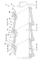
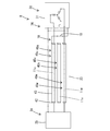
- Example 1 A first embodiment of the present invention will now be described with reference to FIGS. 1 to 3.
- the conductive path A with a noise filter of the first embodiment is provided between the motor 30 and the inverter device 34 mounted on an electric vehicle (not shown) such as an electric car or a hybrid car.
- an electric vehicle not shown
- a motor case 31 which is a case of the motor 30
- an inverter case 35 which is a case of the inverter device 34
- a shield layer 23 connecting both cases 31 and 34 constitute a case ground 36 ing.
- the noise filter-equipped conductive path A includes a U-phase wire 12 u (conductive path body described in the claims), a V-phase wire 12 v (conductive path body described in the claims), and a W-phase wire 12 w that constitute the three-phase AC circuit (Conductive path main body according to claim), U-phase noise filter 15u for reducing surge (noise filter according to claim), V-phase noise filter 15v for reducing surge (noise according to claim) It is configured to include a filter, a W-phase noise filter 15 w for reducing surge (noise filter described in the claims), and a shield layer 23.
- Each of the U-phase wire 12 u, the V-phase wire 12 v, and the W-phase wire 12 w is made of a stranded wire or a single-core wire made of metal (copper, copper alloy, aluminum, aluminum alloy, etc.).
- the outer periphery of the U-phase wire 12 u is surrounded by a synthetic resin U-phase insulating coating 13 u (insulating layer described in the claims).
- the outer periphery of the V-phase wire 12v is surrounded by a synthetic resin V-phase insulating coating 13v (insulating layer described in the claims).
- the outer periphery of the W phase wire 12 w is surrounded by a synthetic resin W phase insulating coating 13 w (insulating layer described in the claims).
- the U-phase wire 12 u and the U-phase insulating coating 13 u constitute one U-phase coated electric wire 11 u.
- V-phase wire 12v and V-phase insulating coating 13v constitute one V-phase coated electric wire 11v.
- W-phase wire 12w and W-phase insulating coating 13w constitute one W-phase coated electric wire 11w.
- the U-phase line 12 u, the V-phase line 12 v and the W-phase line 12 w are wired in parallel.
- One end of each of the U-phase line 12 u, the V-phase line 12 v, and the W-phase line 12 w is connected to an inverter circuit (not shown) of the inverter device 34.
- the inverter circuit is housed inside a conductive inverter case 35 having a shielding function.
- the other ends of U-phase wire 12 u, V-phase wire 12 v, and W-phase wire 12 w are connected to the winding (not shown) of motor 30.
- the windings are housed inside a conductive motor case 31 having a shielding function.
- the U-phase noise filter 15 u is configured to include an electrode of a U-phase capacitor 16 u (a capacitor described in the claims) and an U-phase inductor 22 u (an inductor described in the claims). Specifically, the conductor layer 17 forming the electrode of the U-phase capacitor 16 u and the magnetic layer 20 forming the U-phase inductor 22 u are integrated to form a tape having a constant width.
- the V-phase noise filter 15v also includes an electrode of the V-phase capacitor 16v (capacitor according to the claim) and a V-phase inductor 22v (the inductor according to the claim) It is configured. Specifically, the conductor layer 17 constituting the electrode of the V-phase capacitor 16v and the magnetic layer 20 constituting the V-phase inductor 22v are integrated to form a tape having a predetermined width.
- the W-phase noise filter 15w also includes the electrodes of the W-phase capacitor 16w (capacitor according to the claims) and the W-phase inductor 22w (described in the claims). And an inductor).
- the conductor layer 17 constituting the electrode of the W-phase capacitor 16 w and the magnetic layer 20 constituting the W-phase inductor 22 w are integrated to form a tape having a constant width.
- the conductor layer 17 is made of, for example, a metal foil made of copper, copper alloy, aluminum, aluminum alloy or the like.
- the conductor layer 17 is in the form of a tape having a constant width.
- the magnetic layer 20 is, for example, a flexible base material made of rubber or resin mixed with magnetic powder, and has a tape shape having substantially the same width as the conductor layer 17.
- the magnetic layer 20 is in close contact with the outer surface of the conductor layer 17 by means such as adhesion and welding.
- the conductor layer 17 and the magnetic layer 20 may be easily separated or peeled off without adhering or adhering.
- the side edge portions 17L and 17R of the conductor layer 17 extend to the outer surface side along the outer side surface of the magnetic layer 20, and further extend along the outer surface of the side edge portions 21L and 21R of the magnetic layer 20.
- a pair of folded portions 18L and 18R are integrally formed.
- the folded portions 18L and 18R also have conductivity.
- the folded portions 18L and 18R are also in close contact with the magnetic layer 20 by means such as adhesion or welding.
- the folded portions 18L and 18R and the magnetic layer 20 may be easily separated or peeled off without being in close contact with each other.
- the tape-like U-phase noise filter 15u is spirally wound so as to be in contact with the outer periphery of the U-phase coated electric wire 11u (U-phase insulating coating 13u), and is formed in a cylindrical shape surrounding the U-phase wire 12u There is.
- the V-phase noise filter 15v and the W-phase noise filter 15w also include the V-phase coated wire 11v (V-phase insulating coating 13v) and the W-phase coated wire 11w (W-phase insulating coating 13w) Is spirally wound so as to be in contact with the outer circumference of the cylinder, and is formed in a cylindrical shape surrounding the V phase wire 12v and the W phase wire 12w.
- the outer surface of the folded portion 18R extended from the side edge 17R of one (right side in FIG. 3) of the region of the conductor layer 17 which has been previously wound.
- the inner surface of the side edge 17L of the other (left side in FIG. 3) in the area to be wound later is brought into contact in a superimposed manner. If it winds in this way, a space
- the conductor layer 17 surrounding the U-phase coated electric wire 11u (U-phase wire 12u and U-phase insulating coating 13u) has a positional relationship in close proximity to the U-phase wire 12u across the U-phase insulating coating 13u. There is. Therefore, a U-phase capacitor 16u is constituted by U-phase coated electric wire 11u (U-phase wire 12u and U-phase insulating coating 13u) and conductor layer 17, and U-phase wire 12u and conductor layer 17 function as electrodes.
- V-phase coated electric wire 11v V-phase wire 12v and V-phase insulating coating 13v
- V-phase coated electric wire 11v and V-phase insulating coating 13v constitute V-phase capacitor 16v
- V-phase wire 12v and conductor layer 17 function as electrodes.
- the conductor layer 17 surrounding the W-phase coated electric wire 11w (W-phase wire 12w and the W-phase insulating coating 13w) has a positional relationship in which the W-phase wire 12w is closely opposed to the W-phase wire 12w with the W-phase insulating coating 13w interposed therebetween. It has become. Therefore, W-phase coated wire 11w (W-phase wire 12w and W-phase insulating coating 13w) and conductor layer 17 constitute W-phase capacitor 16w, and W-phase wire 12w and conductor layer 17 function as an electrode.
- the outer periphery of U-phase noise filter 15 u, the outer periphery of V-phase noise filter 15 v, and the outer periphery of W-phase noise filter 15 w are all covered with an insulating coating, an insulating coating, etc. (not shown). . Further, the conductor layer 17 of the U-phase noise filter 15 u, the conductor layer 17 of the V-phase noise filter 15 v, and the conductor layer 17 of the W-phase noise filter 15 w It is connected to the ground 36 (motor case 31).
- each magnetic layer 20 individually surrounds U-phase coated electric wire 11u, V-phase coated electric wire 11v, and W-phase coated electric wire 11w, U-phase inductor 22u, V-phase inductor 22v, W-phase inductor 22w Act as.
- the shield layer 23 is, for example, a metal cylindrical member made of a braided wire or the like. One end of the shield layer 23 is located in the vicinity of the motor 30 and is connected to the motor case 3131 in a conductive manner. The other end of the shield layer 23 is located in the vicinity of the inverter device 34 and is conductively connected to the inverter case 35.
- the space surrounded by the shield layer 23 is a shield space 24.
- the shield layer 23 collectively encloses the U-phase coated electric wire 11u, the V-phase coated electric wire 11v, the W-phase coated electric wire 11w, the U-phase noise filter 15u, the V-phase noise filter 15v, and the W-phase noise filter 15w. .
- the formation range of the conductor layer 17 in the length direction of the conductive path body (U phase wire 12 u, V phase wire 12 v and W phase wire 12 w) (ie, U phase wire 12u, the corresponding area of the conductor layer 17 with respect to the V phase wire 12v and the W phase wire 12w), the distance between the conductor layer 17 and the conductive path body (U phase wire 12u, V phase wire 12v and W phase wire 12w), insulating layer
- the materials of the U-phase insulating coating 13 u, V-phase insulating coating 13 v, W-phase insulating coating 13 w) are appropriately selected, and capacitors 16 u, 16 v, 16 w are suitable for reducing surge noise of the specified frequency. Set the capacity.
- the materials, amounts, and the like of the magnetic powder are appropriately selected for the inductors 22u, 22v, 22w, and the inductances of the inductors 22u, 22v, 22w suitable for reducing the surge noise of the specified frequency are set.
- the capacitances of the capacitors 16u, 16v, 16w and the inductances of the inductors 22u, 22v, 22w are set in this manner, surge current of a specific frequency passes through the inductors 22u, 22v, 22w and the conductor layer connection line 19. Since the current flows to the case ground 36 (motor case 31) and returns to the inverter device 34 via the shield layer 23, surge noise is reduced.
- the conductive path A with noise filter of the first embodiment includes U phase wire 12 u, V phase wire 12 v and W phase wire 12 w, insulating layers 13 u, 13 v, 13 w surrounding each phase wire 12 u, 12 v, 12 w, insulation
- U-phase noise filter 15 u, a V-phase noise filter 15 v, and a W-phase noise filter 15 w provided so as to correspond individually to the outer peripheral surfaces of the layers 13 u, 13 v, 13 w are provided.
- the noise filters 15u, 15v, 15w are disposed to correspond to the U phase line 12u, the V phase line 12v, and the W phase line 12w with the insulating layers 13u, 13v, 13w interposed therebetween.
- the noise filters 15u, 15v, 15w are in the form of a tape, and the U-phase wire 12u (U-phase coated wire 11u), the V-phase wire 12v (V-phase coated wire 11v), the W-phase wire 12w (W-phase coated wire) 11w) is spirally wound.
- the tape-shaped noise filters 15u, 15v, 15w can be used as the U-phase even when the noise filters 15u, 15v, 15w surround the U-phase line 12u, the V-phase line 12v, and the W-phase line 12w. Since it is only necessary to spirally wrap around the coated wire 11u, the V-phase coated wire 11v, and the W-phase coated wire 11w, the workability is excellent.
- the noise filters 15u, 15v, 15w in the form of a tape, it is possible to cope with the bending deformation of the phase wires 12u, 12v, 12w (coated electric wires 11u, 11v, 11w).
- the conductor layer 17 is formed with a folded portion 18R which extends from the one side edge 17R and covers the outer surface of the side edge 21R of the magnetic layer 20. Then, the inner surface of the side edge 17L opposite to the folded portion 18R in the area to be wound later of the conductor layer 17 overlaps the outer surface of the folded area 18R of the area of the conductor layer 17 that is wound first. It is in contact with the condition. According to this configuration, the conductor layers 17 can be reliably brought into contact with each other in a state where the noise filters 15 u, 15 v, 15 w are spirally wound.
- the conductive path main body (U phase wire 12 u, V phase wire 12 v, W phase wire 12 w) and the noise filters 15 u, 15 v, 15 w are collectively surrounded by the cylindrical shield layer 23.
- the motor case 31 and the inverter case 35 are connected by the shield layer 23.
- the conduction means for connecting the motor case 31 and the inverter case 35 is not limited to the shield layer 23, and may be a stranded wire, a single core wire, a vehicle body or the like.
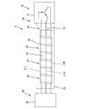
- Example 2 A second embodiment of the present invention will now be described with reference to FIGS. 4 to 5.
- the noise filter attached conductive path B of the second embodiment has a configuration in which the noise filters 40u, 40v, and 40w are different from those of the first embodiment.
- the other parts of the configuration are the same as those of the first embodiment, and thus the same reference numerals are given to the same components, and descriptions of the structures, operations, and effects are omitted.
- the U-phase noise filter 40u, the V-phase noise filter 40v, and the W-phase noise filter 40w according to the second embodiment are not in the form of a tape but in the form of a rectangular sheet, but the conductor layer in which the turnback portion 42 is formed.
- the configuration in which the magnetic material layer 43 is integrated on the outer periphery of 41 is the same as the noise filters 15 u, 15 v, and 15 w of the first embodiment.
- the conductor layer 41 serves as an electrode together with the U-phase wire 12 u, the V-phase wire 12 v, and the W-phase wire 12 w to constitute a U-phase capacitor 44 u, a V-phase capacitor 44 v, and a W-phase capacitor 44 w.
- the magnetic layer 43 constitutes a U-phase inductor 45 u, a V-phase inductor 45 v, and a W-phase inductor 45 w.
- the long sides of the noise filters 40u, 40v, 40w have the same dimensions as the length of the area to be surrounded by the noise filters 40u, 40v, 40w among the U-phase coated electric wire 11u, the V-phase coated electric wire 11v, and the W-phase coated electric wire 11w. It is set. Further, the short sides of the noise filters 40u, 40v, 40w are set to the same dimensions as the circumferential lengths of the coated electric wires 11u, 11v, 11w. And these noise filters 40u, 40v, and 40w are formed in a cylindrical shape by being wound separately on the outer periphery of each coated wire 11u, 11v, and 11w.
- the entire area of the inner surface of the conductor layer 41 may be adhered to the outer peripheral surface of the insulation coatings 13u, 13v, 13w. May be
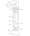
- Example 3 A third embodiment of the present invention will now be described with reference to FIGS.
- the noise filter added conductive path C of the third embodiment has a configuration in which the noise filter 50 is different from that of the first embodiment.
- the other parts of the configuration are the same as in the first and second embodiments, so the same reference numerals are given to the same components, and descriptions of the structures, operations and effects are omitted.
- the U-phase coated electric wire 11 u (U-phase wire 12 u), the V-phase coated electric wire 11 v (V-phase wire 12 v), and the W-phase coated electric wire 11 w (W-phase wire 12 w) It is surrounded.
- the U-phase coated electric wire 11u, the V-phase coated electric wire 11v, and the W-phase coated electric wire 11w are drawn apart, but these three coated electric wires 11u, 11v, 11w , Side-by-side or side-by-side in parallel.
- the noise filter 50 is formed by integrating the magnetic material layer 53 on the outer periphery of the conductor layer 51 on which the folded portion 52 is formed, and has a tape shape. ing.
- the conductor layer 51 serves as an electrode together with the U-phase wire 12 u, the V-phase wire 12 v, and the W-phase wire 12 w to constitute a capacitor 54.
- one capacitor 54 appears as a structure, it has a circuit configuration in which three capacitors 54 are connected in parallel as a circuit.
- the magnetic layer 53 constitutes an inductor 55.
- the noise filter 50 is formed into a tubular shape by spirally winding the U-phase coated electric wire 11 u, the V-phase coated electric wire 11 v, and the W-phase coated electric wire 11 w.
- Example 4 A fourth embodiment of the present invention will now be described with reference to FIGS. 8-9.
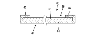
- the conductive path D with a noise filter of the fourth embodiment has a configuration in which the noise filter 60 is different from the first to third embodiments.
- the other parts of the configuration are the same as those of the first to third embodiments, so the same reference numerals are given to the same components, and descriptions of the structures, operations, and effects are omitted.
- the U-phase coated electric wire 11u (U-phase wire 12u), the V-phase coated electric wire 11v (V-phase wire 12v), the W-phase coated electric wire 11w (W-phase) 12w) are collectively enclosed.
- the U-phase coated electric wire 11u, the V-phase coated electric wire 11v, and the W-phase coated electric wire 11w are drawn apart, but these three coated electric wires 11u, 11v, 11w , Side-by-side or side-by-side in parallel.
- the noise filter has a rectangular sheet shape, and has a configuration in which the magnetic layer 63 is integrated on the outer periphery of the conductor layer 61 in which the folded portion 62 is formed.
- the conductor layer 61 serves as an electrode together with the U-phase wire 12 u, the V-phase wire 12 v, and the W-phase wire 12 w to constitute a capacitor 64.
- one capacitor 64 appears as a structure, it has a circuit configuration in which three capacitors 64 are connected in parallel as a circuit.
- the magnetic layer 63 constitutes an inductor 65.
- the long side of the noise filter 60 is set to the same dimension as the length of the area to be surrounded by the noise filter 60 among the U-phase coated electric wire 11 u, the V-phase coated electric wire 11 v, and the W-phase coated electric wire 11 w.
- the short side of the noise filter 60 is set to have a length such that it can be circumscribed around the three coated electric wires 11u, 11v, 11w in a bundled state.
- the noise filter 60 is formed into a tubular shape by being collectively wound around the outer circumferences of the three coated electric wires 11u, 11v, 11w.
- a part of the inner surface of the conductor layer 61 may be in close contact with a part of the outer peripheral surface of the three insulation coatings 13u, 13v, 13w. It does not have to be in close contact.
- the present invention is not limited to the embodiments described above with reference to the drawings.
- the following embodiments are also included in the technical scope of the present invention.
- the pair of folded portions is extended from both side edges of the conductor layer, but the folded portions extend only from any one side edge of the both side edges of the conductor layer. You may let it go out.
- the folded portions are formed from the side edges of the conductor layer. However, such a folded portion may not be formed.
- the plurality of conductive path bodies and the noise filter are collectively surrounded by the shield layer. However, such a shield layer may not be provided.
- the three conductive path bodies constituting the three-phase AC circuit are star connected, but in the present invention, the three conductive path bodies constituting the three-phase AC circuit are It is applicable also when delta connection is carried out.
- the three conductive path bodies constitute the three-phase AC circuit, but in the present invention, the conductive path bodies do not constitute the three-phase AC circuit. It can be applied to (6)
- the number of conductive path bodies is three. However, the present invention can be applied to the case where the number of conductive path bodies is one, two, or four or more.
- the conductive path main body is a stranded wire of a circular cross section having flexibility
- the conductive path main body is a flat in which a plurality of electric wires are arranged in parallel with a bus bar which is not easily deformed. It may be a cable or the like.
- the conductive path with the noise filter is wired between the motor and the inverter, but the present invention is connected to devices other than the motor and the inverter. Can be applied to
- the conductor layer connection wire is connected to the motor case. However, the conductor layer connection wire may be connected directly to the vehicle body instead of the motor case.
- the noise filter is wound around the conductive path main body, but the noise filter is formed in a cylindrical shape, and the conductive path main body is inserted into the cylindrical noise filter You may do it.
- the conductor layer corresponds to the entire periphery of the conductive path body, but the conductive layer is a partial region in the circumferential direction with respect to the conductive path body. It may be in a form corresponding to only one.
- the conductor layer is a tape-like or sheet-like metal foil, but the invention is not limited to this, the conductor layer may be a surface of a braided wire, a sheet core or a tape core.
- the inductor is disposed only on the motor side, and the inductor is connected only to the motor case.
- an inductor is provided on the inverter device side as well.
- An inductor provided on the device side may be connected to the inverter case.
- A, B, C, D Conductive path with noise filter 12 u: U phase wire (conductive path body) 12 v ... V phase wire (conductive path main body) 12w ... W phase wire (conductive path body) 13u ... U phase insulation coating (insulation layer) 13v ... V phase insulation coating (insulation layer) 13w ... W phase insulation coating (insulation layer) 15u, 40u ... U-phase noise filter (noise filter) 15v, 40v ... noise filter for V phase (noise filter) 15w, 40w ... noise filter for W phase (noise filter) 16u, 44u ... U phase capacitor (capacitor) 16v, 44v ... V phase capacitor (capacitor) 16w, 44w ...
Landscapes
- Engineering & Computer Science (AREA)
- Mechanical Engineering (AREA)
- Filters And Equalizers (AREA)
Abstract
特定の周波数帯域のサージノイズを効果的に低減することが可能なノイズフィルタ付き導電路を提供する。 ノイズフィルタ付き導電路(A)は、導電路本体(12u、12v、12w)と、各相線(12u,12v,12w)を包囲する絶縁層(13u,13v,13w)と、絶縁層(13u,13v,13w)の外周面と対応するように設けたノイズフィルタ(15u、15v、15w)とを備える。ノイズフィルタ(15u,15v,15w)は、絶縁層(13u,13v,13w)を挟んで各相線(12u、12v、12w)と対応するように配され、各相線(12u、12v、12w)との間にコンデンサ(16u、16v、16w)を構成する導体層(17)と、導体層(17)の外周に重ねられてインダクタ(22u、22v、22w)を構成する磁性体層(20)とを備える。
Description
本発明は、ノイズフィルタ付き導電路に関するものである。
特許文献1には、電動車両のモータとインバータ装置との間に三相交流電線からなるワイヤーハーネスを配索し、そのワイヤーハーネスにおけるノイズ対策として、ワイヤーハーネスを編組線で包囲し、編組線の両端をモータのシールドケースとインバータ装置のシールドケースとに接続する技術が記載されている。このように、ワイヤーハーネスを編組線でシールドすれば、モータ、インバータ装置、ワイヤーハーネスから放出されるノイズが、周辺の機器や回路に影響を及ぼすことを防止できる。
しかし、ワイヤーハーネスを編組線で包囲する方法では、インバータ装置で発生した特定周波数帯域のサージノイズを効果的に低減することは難しい。
本発明は上記のような事情に基づいて完成されたものであって、特定の周波数帯域のサージノイズを効果的に低減することが可能なノイズフィルタ付き導電路を提供することを目的とする。
本発明は上記のような事情に基づいて完成されたものであって、特定の周波数帯域のサージノイズを効果的に低減することが可能なノイズフィルタ付き導電路を提供することを目的とする。
本発明は、
導電路本体と、
前記導電路本体を包囲する絶縁層と、
前記絶縁層の外周面と対応するように設けたノイズフィルタとを備え、
前記ノイズフィルタは、
前記絶縁層を挟んで前記導電路本体と対応するように配され、前記導電路本体との間にコンデンサを形成する導体層と、
前記導体層の外周に重ねられてインダクタを構成する磁性体層とを備えているところに特徴を有する。
導電路本体と、
前記導電路本体を包囲する絶縁層と、
前記絶縁層の外周面と対応するように設けたノイズフィルタとを備え、
前記ノイズフィルタは、
前記絶縁層を挟んで前記導電路本体と対応するように配され、前記導電路本体との間にコンデンサを形成する導体層と、
前記導体層の外周に重ねられてインダクタを構成する磁性体層とを備えているところに特徴を有する。
導体層の長さ、導体層と導電路本体との対応面積、導体層と導電路本体との距離、絶縁層の材質等を適宜選定してコンデンサの静電容量を設定し、磁性体層の材質、長さ、厚さ等を適宜選定してインダクタのインダクタンスを設定すれば、LC共振により特定の周波数帯域のサージノイズを効果的に低減することができる。
(a)本発明は、前記ノイズフィルタが、テープ状をなしていて前記導電路本体に螺旋状に巻き付けられていてもよい。
この構成によれば、ノイズフィルタで導電路本体を包囲する範囲が長い場合でも、テープ状のノイズフィルタを螺旋状に巻き付けるだけでよいので、作業性に優れている。また、ノイズフィルタをテープ状としたことにより、導電路本体の屈曲変形に対応することが可能である。
この構成によれば、ノイズフィルタで導電路本体を包囲する範囲が長い場合でも、テープ状のノイズフィルタを螺旋状に巻き付けるだけでよいので、作業性に優れている。また、ノイズフィルタをテープ状としたことにより、導電路本体の屈曲変形に対応することが可能である。
(b)本発明は、(a)において、前記導体層には、その一方の側縁部から延出して前記磁性体層の側縁部の外面を覆う折返部が形成されており、前記折返部の外面に対し、前記導体層における前記折返部とは反対側の側縁部の内面が重なった状態で接触していてもよい。
この構成によれば、ノイズフィルタを螺旋巻きした状態で導体層同士を確実に接触させることができる。
この構成によれば、ノイズフィルタを螺旋巻きした状態で導体層同士を確実に接触させることができる。
<実施例1>
以下、本発明を具体化した実施例1を図1~図3を参照して説明する。本実施例1のノイズフィルタ付き導電路Aは、電気自動車又はハイブリッド自動車等の電動車両(図示省略)に搭載されたモータ30とインバータ装置34との間に配索されるものである。この電動車両において、モータ30の筐体であるモータケース31と、インバータ装置34の筐体であるインバータケース35と、両ケース31,34を接続するシールド層23は、筐体アース36を構成している。ノイズフィルタ付き導電路Aは、三相交流回路10を構成するU相線12u(請求項に記載の導電路本体)、V相線12v(請求項に記載の導電路本体)、W相線12w(請求項に記載の導電路本体)と、サージ低減用のU相用ノイズフィルタ15u(請求項に記載のノイズフィルタ)と、サージ低減用のV相用ノイズフィルタ15v(請求項に記載のノイズフィルタ)と、サージ低減用のW相用ノイズフィルタ15w(請求項に記載のノイズフィルタ)と、シールド層23とを備えて構成されている。
以下、本発明を具体化した実施例1を図1~図3を参照して説明する。本実施例1のノイズフィルタ付き導電路Aは、電気自動車又はハイブリッド自動車等の電動車両(図示省略)に搭載されたモータ30とインバータ装置34との間に配索されるものである。この電動車両において、モータ30の筐体であるモータケース31と、インバータ装置34の筐体であるインバータケース35と、両ケース31,34を接続するシールド層23は、筐体アース36を構成している。ノイズフィルタ付き導電路Aは、三相交流回路10を構成するU相線12u(請求項に記載の導電路本体)、V相線12v(請求項に記載の導電路本体)、W相線12w(請求項に記載の導電路本体)と、サージ低減用のU相用ノイズフィルタ15u(請求項に記載のノイズフィルタ)と、サージ低減用のV相用ノイズフィルタ15v(請求項に記載のノイズフィルタ)と、サージ低減用のW相用ノイズフィルタ15w(請求項に記載のノイズフィルタ)と、シールド層23とを備えて構成されている。
U相線12u、V相線12v及びW相線12wは、いずれも、金属(銅、銅合金、アルミニウム、アルミニウム合金等)製の撚り線や単芯線からなる。U相線12uの外周は、合成樹脂製のU相用絶縁被覆13u(請求項に記載の絶縁層)によって包囲されている。V相線12vの外周は、合成樹脂製のV相用絶縁被覆13v(請求項に記載の絶縁層)によって包囲されている。W相線12wの外周は、合成樹脂製のW相用絶縁被覆13w(請求項に記載の絶縁層)によって包囲されている。つまり、U相線12uとU相用絶縁被覆13uは1本のU相被覆電線11uを構成する。V相線12vとV相用絶縁被覆13vは1本のV相被覆電線11vを構成する。W相線12wとW相用絶縁被覆13wは1本のW相被覆電線11wを構成する。
U相線12u、V相線12v及びW相線12wは、並行するように配索されている。U相線12u、V相線12v及びW相線12wの一方の端部は、インバータ装置34のインバータ回路(図示省略)に接続されている。インバータ回路は、シールド機能を有する導電性のインバータケース35の内部に収容されている。U相線12u、V相線12v及びW相線12wの他方の端部は、モータ30の巻線(図示省略)に接続されている。巻線は、シールド機能を有する導電性のモータケース31の内部に収容されている。
U相用ノイズフィルタ15uは、U相用コンデンサ16u(請求項に記載のコンデンサ)の電極とU相用インダクタ22u(請求項に記載のインダクタ)とを備えて構成されている。具体的には、U相用コンデンサ16uの電極を構成する導体層17と、U相用インダクタ22uを構成する磁性体層20とを一体化し、一定幅のテープ状としたものである。
V相用ノイズフィルタ15vも、U相用ノイズフィルタ15uと同様、V相用コンデンサ16v(請求項に記載のコンデンサ)の電極とV相用インダクタ22v(請求項に記載のインダクタ)とを備えて構成されている。具体的には、V相用コンデンサ16vの電極を構成する導体層17と、V相用インダクタ22vを構成する磁性体層20とを一体化し、一定幅のテープ状としたものである。
W相用ノイズフィルタ15wも、U相用ノイズフィルタ15u及びV相用ノイズフィルタ15vと同様、W相用コンデンサ16w(請求項に記載のコンデンサ)の電極とW相用インダクタ22w(請求項に記載のインダクタ)とを備えて構成されている。具体的には、W相用コンデンサ16wの電極を構成する導体層17と、W相用インダクタ22wを構成する磁性体層20とを一体化し、一定幅のテープ状としたものである。
導体層17は、例えば銅製、銅合金製、アルミニウム製、アルミニウム合金製等の金属箔からなる。導体層17は、一定幅のテープ状をなしている。磁性体層20は、例えばゴム又は樹脂製の可撓性を有する母材に磁性体粉を混入したものであり、導体層17とほぼ同じ一定幅のテープ状をなす。磁性体層20は、接着、溶着等の手段により導体層17の外面に密着している。尚、導体層17と磁性体層20は、密着・固着させず、容易に分離したり剥がしたりすることができるようにしてもよい。
導体層17の両側縁部17L,17Rには、磁性体層20の外側面に沿って外面側へ延出し、更に、磁性体層20の側縁部21L,21Rの外面に沿うように延出した一対の折返部18L,18Rが、一体に形成されている。折返部18L,18Rも導電性を有している。また、折返部18L,18Rも、接着や溶着等の手段によって磁性体層20に密着している。尚、折返部18L,18Rと磁性体層20は、密着・固着させず、容易に分離したり剥がしたりすることができるようにしてもよい。
テープ状のU相用ノイズフィルタ15uは、U相被覆電線11u(U相用絶縁被覆13u)の外周に接触するように螺旋状に巻き付けられ、U相線12uを包囲する筒状に成形されている。V相用ノイズフィルタ15vとW相用ノイズフィルタ15wも、U相用ノイズフィルタ15u同様、V相被覆電線11v(V相用絶縁被覆13v)とW相被覆電線11w(W相用絶縁被覆13w)の外周に接触するように螺旋状に巻き付けられ、V相線12vとW相線12wを包囲する筒状に成形されている。
各ノイズフィルタ15u,15v,15wを螺旋状に巻き付ける際には、導体層17のうち先に巻き付けられた領域における一方(図3における右側)の側縁部17Rから延出した折返部18Rの外面に対し、後から巻き付けられる領域における他方(図3における左側)の側縁部17Lの内面を重ね合わせるようにして接触させる。このように巻き付ければ、導体層17のうち先に巻き付けられている領域と、後から巻き付けられる領域との間に隙間が生じることがない。
U相被覆電線11u(U相線12uとU相用絶縁被覆13u)を包囲する導体層17は、U相用絶縁被覆13uを挟んでU相線12uと近接して対向する位置関係となっている。したがって、U相被覆電線11u(U相線12uとU相用絶縁被覆13u)と導体層17によってU相用コンデンサ16uが構成され、U相線12uと導体層17は電極として機能する。
また、V相被覆電線11v(V相線12vとV相用絶縁被覆13v)を包囲する導体層17は、V相用絶縁被覆13vを挟んでV相線12vと近接して対向する位置関係となっている。したがって、V相被覆電線11v(V相線12vとV相用絶縁被覆13v)と導体層17によってV相用コンデンサ16vが構成され、V相線12vと導体層17は電極として機能する。
同様に、W相被覆電線11w(W相線12wとW相用絶縁被覆13w)を包囲する導体層17は、W相用絶縁被覆13wを挟んでW相線12wと近接して対向する位置関係となっている。したがって、W相被覆電線11w(W相線12wとW相用絶縁被覆13w)と導体層17によってW相用コンデンサ16wが構成され、W相線12wと導体層17は電極として機能する。
U相用ノイズフィルタ15uの外周、V相用ノイズフィルタ15vの外周、W相用ノイズフィルタ15wの外周は、いずれも、絶縁性のコーティングや絶縁性の被覆等(図示省略)で覆われている。また、U相用ノイズフィルタ15uの導体層17、V相用ノイズフィルタ15vの導体層17、W相用ノイズフィルタ15wの導体層17は、分岐状の導体層用接続線19を介して筐体アース36(モータケース31)に接続されている。
また、U相用ノイズフィルタ15u、V相用ノイズフィルタ15v、W相用ノイズフィルタ15wを、夫々、U相被覆電線11u、V相被覆電線11v、W相被覆電線11wに螺旋状に巻き付けると、各磁性体層20は、夫々、U相被覆電線11u、V相被覆電線11v、W相被覆電線11wを個別に包囲するので、U相用インダクタ22u、V相用インダクタ22v、W相用インダクタ22wとして機能する。
シールド層23は、例えば、編組線等からなる金属製の筒状部材である。シールド層23の一方の端部は、モータ30の近傍に位置し、モータケース3131に導通可能に接続されている。シールド層23の他方の端部は、インバータ装置34の近傍に位置し、インバータケース35に導通可能に接続されている。そして、シールド層23で包囲された空間は、シールド空間24となっている。シールド層23は、U相被覆電線11u、V相被覆電線11v、W相被覆電線11w、U相用ノイズフィルタ15u、V相用ノイズフィルタ15v、W相用ノイズフィルタ15wを、一括して包囲する。つまり、シールド空間24内には、U相線12u、V相線12v、W相線12wと、U相用コンデンサ16u、V相用コンデンサ16v、W相用コンデンサ16w、U相線用インダクタ、V相用インダクタ22v、W相用インダクタ22wが収容されている。
次に、本実施例1の作用を説明する。インバータ装置34で発生するサージ電圧の周波数を特定したら、導電路本体(U相線12u、V相線12v及びW相線12w)の長さ方向における導体層17の形成範囲(つまり、U相線12u、V相線12v及びW相線12wに対する導体層17の対応面積)、導体層17と導電路本体(U相線12u、V相線12v及びW相線12w)との距離、絶縁層(U相用絶縁被覆13u、V相用絶縁被覆13v、W相用絶縁被覆13w)の材質等を適宜選択し、特定した周波数のサージノイズを低減するのに好適な各コンデンサ16u,16v,16wの容量を設定する。
また、インダクタ22u,22v,22wについても、磁性体粉の材料や量等を適宜選択し、特定した周波数のサージノイズを低減するのに好適なインダクタ22u,22v,22wのインダクタンスを設定する。このようにしてコンデンサ16u,16v,16wの静電容量とインダクタ22u,22v,22wのインダクタンスを設定すると、特定の周波数のサージ電流が、インダクタ22u,22v,22wと導体層用接続線19を経て筐体アース36(モータケース31)に流れ、更にシールド層23を介してインバータ装置34に戻るためサージノイズが低減される。
本実施例1のノイズフィルタ付き導電路Aは、U相線12u、V相線12v及びW相線12wと、各相線12u,12v,12wを包囲する絶縁層13u,13v,13wと、絶縁層13u,13v,13wの外周面と個別に対応するように設けたU相用ノイズフィルタ15u、V相用ノイズフィルタ15v、W相用ノイズフィルタ15wとを備えている。そして、各ノイズフィルタ15u,15v,15wは、絶縁層13u,13v,13wを挟んでU相線12u、V相線12v及びW相線12wと対応するように配され、各相線12u,12v,12wとの間にU相用コンデンサ16u、V相用コンデンサ16v、W相用コンデンサ16wの電極を構成する導体層17と、導体層17の外周に重ねられてU相用インダクタ22u、V相用インダクタ22v、W相用インダクタ22wを構成する磁性体層20とを備えている。この構成によれば、上述のようにしてコンデンサ16u,16v,16wの静電容量を設定するとともにインダクタ22u,22v,22wのインダクタンスを設定すれば、LC共振により特定の周波数帯域のサージノイズを効果的に低減することができる。
また、ノイズフィルタ15u,15v,15wは、テープ状をなしていてU相線12u(U相被覆電線11u)、V相線12v(V相被覆電線11v)、W相線12w(W相被覆電線11w)に螺旋状に巻き付けられている。この構成によれば、ノイズフィルタ15u,15v,15wでU相線12u、V相線12v、W相線12wを包囲する範囲が長い場合でも、テープ状のノイズフィルタ15u,15v,15wをU相被覆電線11u、V相被覆電線11v、W相被覆電線11wに螺旋状に巻き付けるだけでよいので、作業性に優れている。また、ノイズフィルタ15u,15v,15wをテープ状としたことにより、各相線12u,12v,12w(被覆電線11u,11v,11w)の屈曲変形に対応することが可能となっている。
また、導体層17には、その一方の側縁部17Rから延出して磁性体層20の側縁部21Rの外面を覆う折返部18Rが形成されている。そして、導体層17のうち先に巻き付けられている領域の折返部18Rの外面に対し、導体層17のうち後に巻き付けられる領域における折返部18Rとは反対側の側縁部17Lの内面が重なった状態で接触している。この構成によれば、ノイズフィルタ15u,15v,15wを螺旋巻きした状態で導体層17同士を確実に接触させることができる。
また、導電路本体(U相線12u、V相線12v、W相線12w)とノイズフィルタ15u,15v,15wは、筒状のシールド層23によって一括して包囲されている。また、モータケース31とインバータケース35は、シールド層23によって接続されている。尚、モータケース31とインバータケース35を接続する導通手段は、シールド層23に限らず、撚り線、単芯線、車両ボディ等であってもよい。
<実施例2>
次に、本発明を具体化した実施例2を図4~図5を参照して説明する。本実施例2のノイズフィルタ付き導電路Bは、ノイズフィルタ40u,40v,40wを上記実施例1とは異なる構成としたものである。その他の構成については上記実施例1と同じであるため、同じ構成については、同一符号を付し、構造、作用及び効果の説明は省略する。
次に、本発明を具体化した実施例2を図4~図5を参照して説明する。本実施例2のノイズフィルタ付き導電路Bは、ノイズフィルタ40u,40v,40wを上記実施例1とは異なる構成としたものである。その他の構成については上記実施例1と同じであるため、同じ構成については、同一符号を付し、構造、作用及び効果の説明は省略する。
本実施例2のU相用ノイズフィルタ40u、V相用ノイズフィルタ40v、W相用ノイズフィルタ40wは、テープ状ではなく方形のシート状をなしているが、折返部42が形成された導体層41の外周に磁性体層43を重ねて一体化した構成は、実施例1のノイズフィルタ15u,15v,15wと同じである。導体層41は、U相線12u、V相線12v、W相線12wと共に電極となってU相用コンデンサ44u、V相用コンデンサ44v、W相用コンデンサ44wを構成する。また、磁性体層43は、U相用インダクタ45u、V相用インダクタ45v、W相用インダクタ45wを構成する。
各ノイズフィルタ40u,40v,40wの長辺は、U相被覆電線11u、V相被覆電線11v、W相被覆電線11wのうちノイズフィルタ40u,40v,40wで包囲すべき領域の長さと同じ寸法に設定されている。また、各ノイズフィルタ40u,40v,40wの短辺は、各被覆電線11u,11v,11wの周長と同じ寸法に設定されている。そして、これらのノイズフィルタ40u,40v,40wは、各被覆電線11u,11v,11wの外周に個別に巻き付けられることで筒状に成形されている。ノイズフィルタ40u,40v,40wを被覆電線11u,11v,11wに巻き付けた状態では、導体層41の内面の全領域を絶縁被覆13u,13v,13wの外周面に密着させてもよく、密着させなくてもよい。
<実施例3>
次に、本発明を具体化した実施例3を図6~図7を参照して説明する。本実施例3のノイズフィルタ付き導電路Cは、ノイズフィルタ50を上記実施例1とは異なる構成としたものである。その他の構成については上記実施例1,2と同じであるため、同じ構成については、同一符号を付し、構造、作用及び効果の説明は省略する。
次に、本発明を具体化した実施例3を図6~図7を参照して説明する。本実施例3のノイズフィルタ付き導電路Cは、ノイズフィルタ50を上記実施例1とは異なる構成としたものである。その他の構成については上記実施例1,2と同じであるため、同じ構成については、同一符号を付し、構造、作用及び効果の説明は省略する。
本実施例3では、1つのノイズフィルタ50でU相被覆電線11u(U相線12u)、V相被覆電線11v(V相線12v)、W相被覆電線11w(W相線12w)を一括して包囲している。尚、図6では、便宜上、U相被覆電線11uとV相被覆電線11vとW相被覆電線11wが離間しているように描かれているが、これら3本の被覆電線11u,11v,11wは、横並び又は俵積み状に並列配索されている。
ノイズフィルタ50は、実施例1のノイズフィルタ15u,15v,15wと同様、折返部52が形成された導体層51の外周に磁性体層53を重ねて一体化したものであり、テープ状をなしている。導体層51は、U相線12u、V相線12v、W相線12wと共に電極となってコンデンサ54を構成する。尚、コンデンサ54は、構造物としては1つのように見受けられるが、回路としては3つのコンデンサ54が並列した回路構成となっている。また、磁性体層53はインダクタ55を構成する。ノイズフィルタ50は、実施例1と同様、U相被覆電線11u、V相被覆電線11v、W相被覆電線11wに対し螺旋巻きすることによって筒状に成形されている。
<実施例4>
次に、本発明を具体化した実施例4を図8~図9を参照して説明する。本実施例4のノイズフィルタ付き導電路Dは、ノイズフィルタ60を上記実施例1~3とは異なる構成としたものである。その他の構成については上記実施例1~3と同じであるため、同じ構成については、同一符号を付し、構造、作用及び効果の説明は省略する。
次に、本発明を具体化した実施例4を図8~図9を参照して説明する。本実施例4のノイズフィルタ付き導電路Dは、ノイズフィルタ60を上記実施例1~3とは異なる構成としたものである。その他の構成については上記実施例1~3と同じであるため、同じ構成については、同一符号を付し、構造、作用及び効果の説明は省略する。
本実施例4でも、実施例3と同様、1つのノイズフィルタ60でU相被覆電線11u(U相線12u)、V相被覆電線11v(V相線12v)、W相被覆電線11w(W相線12w)を一括して包囲している。尚、図8では、便宜上、U相被覆電線11uとV相被覆電線11vとW相被覆電線11wが離間しているように描かれているが、これら3本の被覆電線11u,11v,11wは、横並び又は俵積み状に並列配索されている。
ノイズフィルタは、実施例2と同様、方形のシート状をなし、折返部62が形成された導体層61の外周に磁性体層63を重ねて一体化した構成である。導体層61は、U相線12u、V相線12v、W相線12wと共に電極となってコンデンサ64を構成する。尚、コンデンサ64は、構造物としては1つのように見受けられるが、回路としては3つのコンデンサ64が並列した回路構成となっている。また、磁性体層63は、インダクタ65を構成する。
ノイズフィルタ60の長辺は、U相被覆電線11u、V相被覆電線11v、W相被覆電線11wのうちノイズフィルタ60で包囲すべき領域の長さと同じ寸法に設定されている。また、ノイズフィルタ60の短辺は、束ねた状態の3本の被覆電線11u,11v,11wに対し外接して一周し得る長さに設定されている。そして、このノイズフィルタ60は、3本の被覆電線11u,11v,11wの外周に一括して巻き付けられることで筒状に成形されている。ノイズフィルタ60を被覆電線11u,11v,11wに巻き付けた状態では、導体層61の内面の一部が、3本の絶縁被覆13u,13v,13wの外周面の一部に密着させてもよく、密着させなくてもよい。
<他の実施例>
本発明は上記記述及び図面によって説明した実施例に限定されるものではなく、例えば次のような実施例も本発明の技術的範囲に含まれる。
(1)上記実施例1~4では、導体層の両側縁から一対の折返部を延出させたが、折返部は、導体層の両側縁部のうちいずれか一方の側縁部だけから延出させてもよい。
(2)上記実施例1~4では、導体層の両側縁部から折り返し状の折返部を形成したが、このような折返部を形成しない形態としてもよい。
(3)上記実施例1~4では、複数本の導電路本体とノイズフィルタをシールド層により一括して包囲したが、このようなシールド層を設けない形態であってもよい。
(4)上記実施例1~4では、三相交流回路を構成する3本の導電路本体がスター結線されているが、本発明は、三相交流回路を構成する3本の導電路本体がデルタ結線されている場合にも適用できる。
(5)上記実施例1~4では、3本の導電路本体が三相交流回路を構成するものであったが、本発明は、導電路本体が三相交流回路を構成しないものである場合にも適用できる。
(6)上記実施例1~4では、導電路本体を3本としたが、本発明は、導電路本体の本数が1本、2本、又は4本以上である場合にも適用できる。
(7)上記実施例1~4では、導電路本体が可撓性を有する円形断面の撚り線であるが、導電路本体は、容易に変形しないバスバーや、複数本の電線を並行配置したフラットケーブル等であってもよい。
(8)上記実施例1~4では、ノイズフィルタ付き導電路が、モータとインバータ装置との間に配索されるものであったが、本発明は、モータやインバータ装置以外の機器に接続される場合にも適用できる。
(9)上記実施例1~4では、導体層用接続線をモータケースに接続したが、導体層用接続線は、モータケースではなく、車両ボディに、直接、接続してもよい。
(10)上記実施例1~4では、ノイズフィルタが導電路本体に巻き付けるようになっているが、ノイズフィルタが筒状に成形されたものであり、筒状のノイズフィルタに導電路本体を挿通するようにしてもよい。
(11)上記実施例1~4では、導体層が導電路本体に対し全周に亘って包囲するように対応しているが、導体層は、導電路本体に対し周方向における一部の領域のみと対応する形態であってもよい。
(12)上記実施例1~4では、導体層をテープ状又はシート状の金属箔としたが、これに限らず、導体層は、編組線、シート状芯材又はテープ状芯材の表面にメッキ処理したもの、シート状又はテープ状の導電性樹脂、シート状又はテープ状の導電性ゴム等からなっていてもよい。
(13)上記実施例1~4では、インダクタをモータ側のみに配置し、そのインダクタをモータケースのみに接続したが、モータ側のインダクタの他に、インバータ装置側にもインダクタを設け、そのインバータ装置側に設けたインダクタをインバータケースに接続してもよい。
本発明は上記記述及び図面によって説明した実施例に限定されるものではなく、例えば次のような実施例も本発明の技術的範囲に含まれる。
(1)上記実施例1~4では、導体層の両側縁から一対の折返部を延出させたが、折返部は、導体層の両側縁部のうちいずれか一方の側縁部だけから延出させてもよい。
(2)上記実施例1~4では、導体層の両側縁部から折り返し状の折返部を形成したが、このような折返部を形成しない形態としてもよい。
(3)上記実施例1~4では、複数本の導電路本体とノイズフィルタをシールド層により一括して包囲したが、このようなシールド層を設けない形態であってもよい。
(4)上記実施例1~4では、三相交流回路を構成する3本の導電路本体がスター結線されているが、本発明は、三相交流回路を構成する3本の導電路本体がデルタ結線されている場合にも適用できる。
(5)上記実施例1~4では、3本の導電路本体が三相交流回路を構成するものであったが、本発明は、導電路本体が三相交流回路を構成しないものである場合にも適用できる。
(6)上記実施例1~4では、導電路本体を3本としたが、本発明は、導電路本体の本数が1本、2本、又は4本以上である場合にも適用できる。
(7)上記実施例1~4では、導電路本体が可撓性を有する円形断面の撚り線であるが、導電路本体は、容易に変形しないバスバーや、複数本の電線を並行配置したフラットケーブル等であってもよい。
(8)上記実施例1~4では、ノイズフィルタ付き導電路が、モータとインバータ装置との間に配索されるものであったが、本発明は、モータやインバータ装置以外の機器に接続される場合にも適用できる。
(9)上記実施例1~4では、導体層用接続線をモータケースに接続したが、導体層用接続線は、モータケースではなく、車両ボディに、直接、接続してもよい。
(10)上記実施例1~4では、ノイズフィルタが導電路本体に巻き付けるようになっているが、ノイズフィルタが筒状に成形されたものであり、筒状のノイズフィルタに導電路本体を挿通するようにしてもよい。
(11)上記実施例1~4では、導体層が導電路本体に対し全周に亘って包囲するように対応しているが、導体層は、導電路本体に対し周方向における一部の領域のみと対応する形態であってもよい。
(12)上記実施例1~4では、導体層をテープ状又はシート状の金属箔としたが、これに限らず、導体層は、編組線、シート状芯材又はテープ状芯材の表面にメッキ処理したもの、シート状又はテープ状の導電性樹脂、シート状又はテープ状の導電性ゴム等からなっていてもよい。
(13)上記実施例1~4では、インダクタをモータ側のみに配置し、そのインダクタをモータケースのみに接続したが、モータ側のインダクタの他に、インバータ装置側にもインダクタを設け、そのインバータ装置側に設けたインダクタをインバータケースに接続してもよい。
A、B、C、D…ノイズフィルタ付き導電路
12u…U相線(導電路本体)
12v…V相線(導電路本体)
12w…W相線(導電路本体)
13u…U相用絶縁被覆(絶縁層)
13v…V相用絶縁被覆(絶縁層)
13w…W相用絶縁被覆(絶縁層)
15u、40u…U相用ノイズフィルタ(ノイズフィルタ)
15v、40v…V相用ノイズフィルタ(ノイズフィルタ)
15w、40w…W相用ノイズフィルタ(ノイズフィルタ)
16u、44u…U相用コンデンサ(コンデンサ)
16v、44v…V相用コンデンサ(コンデンサ)
16w、44w…W相用コンデンサ(コンデンサ)
17、41、51、61…導体層
17L…導体層における折返部とは反対側の側縁部
17R…導体層の一方の側縁部
18L,18R、42、52、62…折返部
20、43、53、63…磁性体層
21R…磁性体層の側縁部
22u、45u…U相用インダクタ(インダクタ)
22v、45v…V相用インダクタ(インダクタ)
22w、45w…W相用インダクタ(インダクタ)
50、60…ノイズフィルタ
54、64…コンデンサ
55、65…インダクタ
12u…U相線(導電路本体)
12v…V相線(導電路本体)
12w…W相線(導電路本体)
13u…U相用絶縁被覆(絶縁層)
13v…V相用絶縁被覆(絶縁層)
13w…W相用絶縁被覆(絶縁層)
15u、40u…U相用ノイズフィルタ(ノイズフィルタ)
15v、40v…V相用ノイズフィルタ(ノイズフィルタ)
15w、40w…W相用ノイズフィルタ(ノイズフィルタ)
16u、44u…U相用コンデンサ(コンデンサ)
16v、44v…V相用コンデンサ(コンデンサ)
16w、44w…W相用コンデンサ(コンデンサ)
17、41、51、61…導体層
17L…導体層における折返部とは反対側の側縁部
17R…導体層の一方の側縁部
18L,18R、42、52、62…折返部
20、43、53、63…磁性体層
21R…磁性体層の側縁部
22u、45u…U相用インダクタ(インダクタ)
22v、45v…V相用インダクタ(インダクタ)
22w、45w…W相用インダクタ(インダクタ)
50、60…ノイズフィルタ
54、64…コンデンサ
55、65…インダクタ
Claims (3)
- 導電路本体と、
前記導電路本体を包囲する絶縁層と、
前記絶縁層の外周面と対応するように設けたノイズフィルタとを備え、
前記ノイズフィルタは、
前記絶縁層を挟んで前記導電路本体と対応するように配され、前記導電路本体との間にコンデンサを形成する導体層と、
前記導体層の外周に重ねられてインダクタを構成する磁性体層とを備えていることを特徴とするノイズフィルタ付き導電路。 - 前記ノイズフィルタが、テープ状をなしていて前記導電路本体に螺旋状に巻き付けられていることを特徴とする請求項1記載のノイズフィルタ付き導電路。
- 前記導体層には、その一方の側縁部から延出して前記磁性体層の側縁部の外面を覆う折返部が形成されており、
前記折返部の外面に対し、前記導体層における前記折返部とは反対側の側縁部の内面が重なった状態で接触していることを特徴とする請求項2記載のノイズフィルタ付き導電路。
Applications Claiming Priority (2)
| Application Number | Priority Date | Filing Date | Title |
|---|---|---|---|
| JP2015137833A JP2017022517A (ja) | 2015-07-09 | 2015-07-09 | ノイズフィルタ付き導電路 |
| JP2015-137833 | 2015-07-09 |
Publications (1)
| Publication Number | Publication Date |
|---|---|
| WO2017006753A1 true WO2017006753A1 (ja) | 2017-01-12 |
Family
ID=57685576
Family Applications (1)
| Application Number | Title | Priority Date | Filing Date |
|---|---|---|---|
| PCT/JP2016/068224 Ceased WO2017006753A1 (ja) | 2015-07-09 | 2016-06-20 | ノイズフィルタ付き導電路 |
Country Status (2)
| Country | Link |
|---|---|
| JP (1) | JP2017022517A (ja) |
| WO (1) | WO2017006753A1 (ja) |
Citations (3)
| Publication number | Priority date | Publication date | Assignee | Title |
|---|---|---|---|---|
| JPS59125122U (ja) * | 1983-02-10 | 1984-08-23 | 東北金属工業株式会社 | ノイズ防止装置 |
| JPH0320426U (ja) * | 1989-07-05 | 1991-02-28 | ||
| JP2013109935A (ja) * | 2011-11-21 | 2013-06-06 | Yazaki Corp | 高圧導電路及びワイヤハーネス |
-
2015
- 2015-07-09 JP JP2015137833A patent/JP2017022517A/ja active Pending
-
2016
- 2016-06-20 WO PCT/JP2016/068224 patent/WO2017006753A1/ja not_active Ceased
Patent Citations (3)
| Publication number | Priority date | Publication date | Assignee | Title |
|---|---|---|---|---|
| JPS59125122U (ja) * | 1983-02-10 | 1984-08-23 | 東北金属工業株式会社 | ノイズ防止装置 |
| JPH0320426U (ja) * | 1989-07-05 | 1991-02-28 | ||
| JP2013109935A (ja) * | 2011-11-21 | 2013-06-06 | Yazaki Corp | 高圧導電路及びワイヤハーネス |
Also Published As
| Publication number | Publication date |
|---|---|
| JP2017022517A (ja) | 2017-01-26 |
Similar Documents
| Publication | Publication Date | Title |
|---|---|---|
| JP5850356B1 (ja) | ノイズフィルタ付き導電路 | |
| JP5216265B2 (ja) | インダクタンス素子、フィルタ回路及びノイズフィルタ | |
| US9783136B2 (en) | Wire harness | |
| JP6418095B2 (ja) | シールド導電路 | |
| JP5850357B1 (ja) | ノイズフィルタ付き導電路 | |
| JP5850355B1 (ja) | ノイズフィルタ付き導電路 | |
| JP6631389B2 (ja) | ノイズフィルタ付き導電路 | |
| WO2017006753A1 (ja) | ノイズフィルタ付き導電路 | |
| CN113812067B (zh) | 定子线圈、具备该定子线圈的定子以及旋转电机、定子线圈的制造方法 | |
| JP4987506B2 (ja) | インダクタンス素子及びそれを用いたノイズフィルタ | |
| JP6631386B2 (ja) | ノイズフィルタ付き導電路 | |
| WO2017056886A1 (ja) | ノイズフィルタ付き導電路 | |
| JP2008098307A (ja) | インダクタンス素子 | |
| JP2005160058A (ja) | フィルタ素子 | |
| CN112820520B (zh) | 一种电屏蔽带、应用于线圈的电屏蔽结构及其制作方法 | |
| JP2008098305A (ja) | インダクタンス素子 | |
| JP2007067982A (ja) | フィルタ素子 | |
| JPH0247099B2 (ja) | Fuirumukondensa |
Legal Events
| Date | Code | Title | Description |
|---|---|---|---|
| 121 | Ep: the epo has been informed by wipo that ep was designated in this application |
Ref document number: 16821223 Country of ref document: EP Kind code of ref document: A1 |
|
| NENP | Non-entry into the national phase |
Ref country code: DE |
|
| 122 | Ep: pct application non-entry in european phase |
Ref document number: 16821223 Country of ref document: EP Kind code of ref document: A1 |