WO2017002200A1 - 半導体装置 - Google Patents
半導体装置 Download PDFInfo
- Publication number
- WO2017002200A1 WO2017002200A1 PCT/JP2015/068836 JP2015068836W WO2017002200A1 WO 2017002200 A1 WO2017002200 A1 WO 2017002200A1 JP 2015068836 W JP2015068836 W JP 2015068836W WO 2017002200 A1 WO2017002200 A1 WO 2017002200A1
- Authority
- WO
- WIPO (PCT)
- Prior art keywords
- layer
- wiring
- substrate
- pad
- semiconductor
- Prior art date
- Legal status (The legal status is an assumption and is not a legal conclusion. Google has not performed a legal analysis and makes no representation as to the accuracy of the status listed.)
- Ceased
Links
Images






Classifications
-
- H—ELECTRICITY
- H10—SEMICONDUCTOR DEVICES; ELECTRIC SOLID-STATE DEVICES NOT OTHERWISE PROVIDED FOR
- H10W—GENERIC PACKAGES, INTERCONNECTIONS, CONNECTORS OR OTHER CONSTRUCTIONAL DETAILS OF DEVICES COVERED BY CLASS H10
- H10W42/00—Arrangements for protection of devices
-
- H—ELECTRICITY
- H10—SEMICONDUCTOR DEVICES; ELECTRIC SOLID-STATE DEVICES NOT OTHERWISE PROVIDED FOR
- H10F—INORGANIC SEMICONDUCTOR DEVICES SENSITIVE TO INFRARED RADIATION, LIGHT, ELECTROMAGNETIC RADIATION OF SHORTER WAVELENGTH OR CORPUSCULAR RADIATION
- H10F39/00—Integrated devices, or assemblies of multiple devices, comprising at least one element covered by group H10F30/00, e.g. radiation detectors comprising photodiode arrays
- H10F39/80—Constructional details of image sensors
- H10F39/811—Interconnections
-
- H—ELECTRICITY
- H10—SEMICONDUCTOR DEVICES; ELECTRIC SOLID-STATE DEVICES NOT OTHERWISE PROVIDED FOR
- H10W—GENERIC PACKAGES, INTERCONNECTIONS, CONNECTORS OR OTHER CONSTRUCTIONAL DETAILS OF DEVICES COVERED BY CLASS H10
- H10W20/00—Interconnections in chips, wafers or substrates
- H10W20/20—Interconnections within wafers or substrates, e.g. through-silicon vias [TSV]
-
- H—ELECTRICITY
- H10—SEMICONDUCTOR DEVICES; ELECTRIC SOLID-STATE DEVICES NOT OTHERWISE PROVIDED FOR
- H10W—GENERIC PACKAGES, INTERCONNECTIONS, CONNECTORS OR OTHER CONSTRUCTIONAL DETAILS OF DEVICES COVERED BY CLASS H10
- H10W20/00—Interconnections in chips, wafers or substrates
- H10W20/40—Interconnections external to wafers or substrates, e.g. back-end-of-line [BEOL] metallisations or vias connecting to gate electrodes
- H10W20/41—Interconnections external to wafers or substrates, e.g. back-end-of-line [BEOL] metallisations or vias connecting to gate electrodes characterised by their conductive parts
- H10W20/42—Vias, e.g. via plugs
-
- H—ELECTRICITY
- H10—SEMICONDUCTOR DEVICES; ELECTRIC SOLID-STATE DEVICES NOT OTHERWISE PROVIDED FOR
- H10W—GENERIC PACKAGES, INTERCONNECTIONS, CONNECTORS OR OTHER CONSTRUCTIONAL DETAILS OF DEVICES COVERED BY CLASS H10
- H10W72/00—Interconnections or connectors in packages
- H10W72/20—Bump connectors, e.g. solder bumps or copper pillars; Dummy bumps; Thermal bumps
-
- H—ELECTRICITY
- H10—SEMICONDUCTOR DEVICES; ELECTRIC SOLID-STATE DEVICES NOT OTHERWISE PROVIDED FOR
- H10W—GENERIC PACKAGES, INTERCONNECTIONS, CONNECTORS OR OTHER CONSTRUCTIONAL DETAILS OF DEVICES COVERED BY CLASS H10
- H10W72/00—Interconnections or connectors in packages
- H10W72/90—Bond pads, in general
-
- H—ELECTRICITY
- H10—SEMICONDUCTOR DEVICES; ELECTRIC SOLID-STATE DEVICES NOT OTHERWISE PROVIDED FOR
- H10W—GENERIC PACKAGES, INTERCONNECTIONS, CONNECTORS OR OTHER CONSTRUCTIONAL DETAILS OF DEVICES COVERED BY CLASS H10
- H10W74/00—Encapsulations, e.g. protective coatings
- H10W74/10—Encapsulations, e.g. protective coatings characterised by their shape or disposition
- H10W74/111—Encapsulations, e.g. protective coatings characterised by their shape or disposition the semiconductor body being completely enclosed
- H10W74/129—Encapsulations, e.g. protective coatings characterised by their shape or disposition the semiconductor body being completely enclosed forming a chip-scale package [CSP]
-
- H—ELECTRICITY
- H10—SEMICONDUCTOR DEVICES; ELECTRIC SOLID-STATE DEVICES NOT OTHERWISE PROVIDED FOR
- H10W—GENERIC PACKAGES, INTERCONNECTIONS, CONNECTORS OR OTHER CONSTRUCTIONAL DETAILS OF DEVICES COVERED BY CLASS H10
- H10W74/00—Encapsulations, e.g. protective coatings
- H10W74/40—Encapsulations, e.g. protective coatings characterised by their materials
-
- H—ELECTRICITY
- H10—SEMICONDUCTOR DEVICES; ELECTRIC SOLID-STATE DEVICES NOT OTHERWISE PROVIDED FOR
- H10W—GENERIC PACKAGES, INTERCONNECTIONS, CONNECTORS OR OTHER CONSTRUCTIONAL DETAILS OF DEVICES COVERED BY CLASS H10
- H10W90/00—Package configurations
-
- H—ELECTRICITY
- H10—SEMICONDUCTOR DEVICES; ELECTRIC SOLID-STATE DEVICES NOT OTHERWISE PROVIDED FOR
- H10W—GENERIC PACKAGES, INTERCONNECTIONS, CONNECTORS OR OTHER CONSTRUCTIONAL DETAILS OF DEVICES COVERED BY CLASS H10
- H10W72/00—Interconnections or connectors in packages
- H10W72/01—Manufacture or treatment
- H10W72/0198—Manufacture or treatment batch processes
-
- H—ELECTRICITY
- H10—SEMICONDUCTOR DEVICES; ELECTRIC SOLID-STATE DEVICES NOT OTHERWISE PROVIDED FOR
- H10W—GENERIC PACKAGES, INTERCONNECTIONS, CONNECTORS OR OTHER CONSTRUCTIONAL DETAILS OF DEVICES COVERED BY CLASS H10
- H10W72/00—Interconnections or connectors in packages
- H10W72/071—Connecting or disconnecting
- H10W72/072—Connecting or disconnecting of bump connectors
- H10W72/07251—Connecting or disconnecting of bump connectors characterised by changes in properties of the bump connectors during connecting
- H10W72/07254—Connecting or disconnecting of bump connectors characterised by changes in properties of the bump connectors during connecting changes in dispositions
-
- H—ELECTRICITY
- H10—SEMICONDUCTOR DEVICES; ELECTRIC SOLID-STATE DEVICES NOT OTHERWISE PROVIDED FOR
- H10W—GENERIC PACKAGES, INTERCONNECTIONS, CONNECTORS OR OTHER CONSTRUCTIONAL DETAILS OF DEVICES COVERED BY CLASS H10
- H10W72/00—Interconnections or connectors in packages
- H10W72/20—Bump connectors, e.g. solder bumps or copper pillars; Dummy bumps; Thermal bumps
- H10W72/221—Structures or relative sizes
-
- H—ELECTRICITY
- H10—SEMICONDUCTOR DEVICES; ELECTRIC SOLID-STATE DEVICES NOT OTHERWISE PROVIDED FOR
- H10W—GENERIC PACKAGES, INTERCONNECTIONS, CONNECTORS OR OTHER CONSTRUCTIONAL DETAILS OF DEVICES COVERED BY CLASS H10
- H10W72/00—Interconnections or connectors in packages
- H10W72/20—Bump connectors, e.g. solder bumps or copper pillars; Dummy bumps; Thermal bumps
- H10W72/241—Dispositions, e.g. layouts
- H10W72/247—Dispositions of multiple bumps
-
- H—ELECTRICITY
- H10—SEMICONDUCTOR DEVICES; ELECTRIC SOLID-STATE DEVICES NOT OTHERWISE PROVIDED FOR
- H10W—GENERIC PACKAGES, INTERCONNECTIONS, CONNECTORS OR OTHER CONSTRUCTIONAL DETAILS OF DEVICES COVERED BY CLASS H10
- H10W72/00—Interconnections or connectors in packages
- H10W72/20—Bump connectors, e.g. solder bumps or copper pillars; Dummy bumps; Thermal bumps
- H10W72/251—Materials
- H10W72/252—Materials comprising solid metals or solid metalloids, e.g. PbSn, Ag or Cu
-
- H—ELECTRICITY
- H10—SEMICONDUCTOR DEVICES; ELECTRIC SOLID-STATE DEVICES NOT OTHERWISE PROVIDED FOR
- H10W—GENERIC PACKAGES, INTERCONNECTIONS, CONNECTORS OR OTHER CONSTRUCTIONAL DETAILS OF DEVICES COVERED BY CLASS H10
- H10W72/00—Interconnections or connectors in packages
- H10W72/20—Bump connectors, e.g. solder bumps or copper pillars; Dummy bumps; Thermal bumps
- H10W72/29—Bond pads specially adapted therefor
-
- H—ELECTRICITY
- H10—SEMICONDUCTOR DEVICES; ELECTRIC SOLID-STATE DEVICES NOT OTHERWISE PROVIDED FOR
- H10W—GENERIC PACKAGES, INTERCONNECTIONS, CONNECTORS OR OTHER CONSTRUCTIONAL DETAILS OF DEVICES COVERED BY CLASS H10
- H10W72/00—Interconnections or connectors in packages
- H10W72/30—Die-attach connectors
- H10W72/351—Materials of die-attach connectors
- H10W72/353—Materials of die-attach connectors not comprising solid metals or solid metalloids, e.g. ceramics
- H10W72/354—Materials of die-attach connectors not comprising solid metals or solid metalloids, e.g. ceramics comprising polymers
-
- H—ELECTRICITY
- H10—SEMICONDUCTOR DEVICES; ELECTRIC SOLID-STATE DEVICES NOT OTHERWISE PROVIDED FOR
- H10W—GENERIC PACKAGES, INTERCONNECTIONS, CONNECTORS OR OTHER CONSTRUCTIONAL DETAILS OF DEVICES COVERED BY CLASS H10
- H10W72/00—Interconnections or connectors in packages
- H10W72/90—Bond pads, in general
- H10W72/921—Structures or relative sizes of bond pads
- H10W72/923—Bond pads having multiple stacked layers
-
- H—ELECTRICITY
- H10—SEMICONDUCTOR DEVICES; ELECTRIC SOLID-STATE DEVICES NOT OTHERWISE PROVIDED FOR
- H10W—GENERIC PACKAGES, INTERCONNECTIONS, CONNECTORS OR OTHER CONSTRUCTIONAL DETAILS OF DEVICES COVERED BY CLASS H10
- H10W72/00—Interconnections or connectors in packages
- H10W72/90—Bond pads, in general
- H10W72/941—Dispositions of bond pads
- H10W72/9415—Dispositions of bond pads relative to the surface, e.g. recessed, protruding
-
- H—ELECTRICITY
- H10—SEMICONDUCTOR DEVICES; ELECTRIC SOLID-STATE DEVICES NOT OTHERWISE PROVIDED FOR
- H10W—GENERIC PACKAGES, INTERCONNECTIONS, CONNECTORS OR OTHER CONSTRUCTIONAL DETAILS OF DEVICES COVERED BY CLASS H10
- H10W72/00—Interconnections or connectors in packages
- H10W72/90—Bond pads, in general
- H10W72/941—Dispositions of bond pads
- H10W72/942—Dispositions of bond pads relative to underlying supporting features, e.g. bond pads, RDLs or vias
-
- H—ELECTRICITY
- H10—SEMICONDUCTOR DEVICES; ELECTRIC SOLID-STATE DEVICES NOT OTHERWISE PROVIDED FOR
- H10W—GENERIC PACKAGES, INTERCONNECTIONS, CONNECTORS OR OTHER CONSTRUCTIONAL DETAILS OF DEVICES COVERED BY CLASS H10
- H10W72/00—Interconnections or connectors in packages
- H10W72/90—Bond pads, in general
- H10W72/941—Dispositions of bond pads
- H10W72/944—Dispositions of multiple bond pads
-
- H—ELECTRICITY
- H10—SEMICONDUCTOR DEVICES; ELECTRIC SOLID-STATE DEVICES NOT OTHERWISE PROVIDED FOR
- H10W—GENERIC PACKAGES, INTERCONNECTIONS, CONNECTORS OR OTHER CONSTRUCTIONAL DETAILS OF DEVICES COVERED BY CLASS H10
- H10W72/00—Interconnections or connectors in packages
- H10W72/90—Bond pads, in general
- H10W72/951—Materials of bond pads
- H10W72/952—Materials of bond pads comprising metals or metalloids, e.g. PbSn, Ag or Cu
-
- H—ELECTRICITY
- H10—SEMICONDUCTOR DEVICES; ELECTRIC SOLID-STATE DEVICES NOT OTHERWISE PROVIDED FOR
- H10W—GENERIC PACKAGES, INTERCONNECTIONS, CONNECTORS OR OTHER CONSTRUCTIONAL DETAILS OF DEVICES COVERED BY CLASS H10
- H10W74/00—Encapsulations, e.g. protective coatings
- H10W74/10—Encapsulations, e.g. protective coatings characterised by their shape or disposition
- H10W74/131—Encapsulations, e.g. protective coatings characterised by their shape or disposition the semiconductor body being only partially enclosed
- H10W74/142—Encapsulations, e.g. protective coatings characterised by their shape or disposition the semiconductor body being only partially enclosed the encapsulations exposing the passive side of the semiconductor body
-
- H—ELECTRICITY
- H10—SEMICONDUCTOR DEVICES; ELECTRIC SOLID-STATE DEVICES NOT OTHERWISE PROVIDED FOR
- H10W—GENERIC PACKAGES, INTERCONNECTIONS, CONNECTORS OR OTHER CONSTRUCTIONAL DETAILS OF DEVICES COVERED BY CLASS H10
- H10W74/00—Encapsulations, e.g. protective coatings
- H10W74/10—Encapsulations, e.g. protective coatings characterised by their shape or disposition
- H10W74/15—Encapsulations, e.g. protective coatings characterised by their shape or disposition on active surfaces of flip-chip devices, e.g. underfills
-
- H—ELECTRICITY
- H10—SEMICONDUCTOR DEVICES; ELECTRIC SOLID-STATE DEVICES NOT OTHERWISE PROVIDED FOR
- H10W—GENERIC PACKAGES, INTERCONNECTIONS, CONNECTORS OR OTHER CONSTRUCTIONAL DETAILS OF DEVICES COVERED BY CLASS H10
- H10W90/00—Package configurations
- H10W90/20—Configurations of stacked chips
- H10W90/26—Configurations of stacked chips the stacked chips being of the same size without any chips being laterally offset, e.g. chip stacks having a rectangular shape
-
- H—ELECTRICITY
- H10—SEMICONDUCTOR DEVICES; ELECTRIC SOLID-STATE DEVICES NOT OTHERWISE PROVIDED FOR
- H10W—GENERIC PACKAGES, INTERCONNECTIONS, CONNECTORS OR OTHER CONSTRUCTIONAL DETAILS OF DEVICES COVERED BY CLASS H10
- H10W90/00—Package configurations
- H10W90/20—Configurations of stacked chips
- H10W90/291—Configurations of stacked chips characterised by containers, encapsulations, or other housings for the stacked chips
-
- H—ELECTRICITY
- H10—SEMICONDUCTOR DEVICES; ELECTRIC SOLID-STATE DEVICES NOT OTHERWISE PROVIDED FOR
- H10W—GENERIC PACKAGES, INTERCONNECTIONS, CONNECTORS OR OTHER CONSTRUCTIONAL DETAILS OF DEVICES COVERED BY CLASS H10
- H10W90/00—Package configurations
- H10W90/701—Package configurations characterised by the relative positions of pads or connectors relative to package parts
- H10W90/721—Package configurations characterised by the relative positions of pads or connectors relative to package parts of bump connectors
- H10W90/722—Package configurations characterised by the relative positions of pads or connectors relative to package parts of bump connectors between stacked chips
-
- H—ELECTRICITY
- H10—SEMICONDUCTOR DEVICES; ELECTRIC SOLID-STATE DEVICES NOT OTHERWISE PROVIDED FOR
- H10W—GENERIC PACKAGES, INTERCONNECTIONS, CONNECTORS OR OTHER CONSTRUCTIONAL DETAILS OF DEVICES COVERED BY CLASS H10
- H10W90/00—Package configurations
- H10W90/701—Package configurations characterised by the relative positions of pads or connectors relative to package parts
- H10W90/731—Package configurations characterised by the relative positions of pads or connectors relative to package parts of die-attach connectors
- H10W90/732—Package configurations characterised by the relative positions of pads or connectors relative to package parts of die-attach connectors between stacked chips
Definitions
- the present invention relates to a semiconductor device.
- FIG. 20 illustrates a configuration of a semiconductor device 1010 having a plurality of substrates.
- FIG. 20 shows a cross section of the semiconductor device 1010.
- the semiconductor device 1010 includes a first substrate 1100, a second substrate 1200, and a connection portion 1300.
- the first substrate 1100 and the second substrate 1200 are connected via a connection portion 1300.
- the first substrate 1100 and the second substrate 1200 are stacked in the thickness direction Dr1001 of the first substrate 1100.
- the first substrate 1100 includes a first semiconductor layer 1110 and a first wiring layer 1120.
- the first semiconductor layer 1110 and the first wiring layer 1120 overlap the thickness direction Dr1001 of the first substrate 1100.
- the first semiconductor layer 1110 and the first wiring layer 1120 are in contact with each other.
- the first wiring layer 1120 includes a first wiring 1121, a first via 1122, and a first interlayer insulating film 1123.
- first wiring 1121 there are a plurality of first wirings 1121, but a reference numeral of one first wiring 1121 is shown as a representative.
- first vias 1122 there are a plurality of first vias 1122 in FIG. 20, the reference numerals of one first via 1122 are shown as representatives.
- the first wiring 1121 is a thin film on which a wiring pattern is formed.
- the first wiring 1121 transmits a signal.
- a two-layer first wiring 1121 is formed.
- the first via 1122 connects the first wirings 1121 of different layers.
- portions other than the first wiring 1121 and the first via 1122 are configured by a first interlayer insulating film 1123.
- the second substrate 1200 includes a second semiconductor layer 1210 and a second wiring layer 1220.
- the second semiconductor layer 1210 and the second wiring layer 1220 overlap in the thickness direction Dr1001. Further, the second semiconductor layer 1210 and the second wiring layer 1220 are in contact with each other.
- the second wiring layer 1220 includes a second wiring 1221, a second via 1222, and a second interlayer insulating film 1223.
- FIG. 20 there are a plurality of second wirings 1221, but a symbol of one second wiring 1221 is shown as a representative.
- FIG. 20 the reference numerals of one second via 1222 are shown as representatives.
- the second wiring 1221 is a thin film on which a wiring pattern is formed.
- the second wiring 1221 transmits a signal.
- a two-layer second wiring 1221 is formed.
- the second via 1222 connects the second wiring 1221 of different layers.
- portions other than the second wiring 1221 and the second via 1222 are configured by the second interlayer insulating film 1223.
- the first substrate 1100 and the second substrate 1200 are arranged so that the first wiring layer 1120 and the second wiring layer 1220 face each other.
- the connection portion 1300 is disposed between the first wiring layer 1120 and the second wiring layer 1220.
- the connection portion 1300 electrically connects the first wiring 1121 and the second wiring 1221.
- the connection portion 1300 includes a first pad 1301, a second pad 1302, a micro bump 1303, and a resin layer 1304.
- first pads 1301, but a reference numeral of one first pad 1301 is shown as a representative.
- second pads 1302, but a symbol of one second pad 1302 is shown as a representative.
- there are a plurality of micro bumps 1303, but a reference numeral of one micro bump 1303 is shown as a representative.
- the first pad 1301 is a thin film.
- the first pad 1301 is disposed on the surface of the first wiring layer 1120.
- the first pad 1301 is in contact with the first via 1122 on the surface of the first wiring layer 1120. For this reason, the first pad 1301 is electrically connected to the first wiring 1121.
- the second pad 1302 is a thin film.
- the second pad 1302 is disposed on the surface of the second wiring layer 1220.
- the second pad 1302 is in contact with the second via 1222 on the surface of the second wiring layer 1220. Therefore, the second pad 1302 is electrically connected to the second wiring 1221.
- the micro bump 1303 is a columnar structure.
- the micro bump 1303 is disposed between the first pad 1301 and the second pad 1302 and is electrically connected to the first pad 1301 and the second pad 1302.
- the first pad 1301, the second pad 1302, and the micro bump 1303 are electrically connected to the first wiring 1121 and the second wiring 1221, and the first substrate 1100 Signals are transmitted to and from the second substrate 1200.
- the resin layer 1304 is disposed between the first wiring layer 1120 and the second wiring layer 1220.
- the resin layer 1304 is made of an underfill resin.
- the resin layer 1304 covers the surfaces of the first pad 1301, the second pad 1302, and the micro bump 1303.
- the first substrate 1100 and the second substrate 1200 are connected only by the first pad 1301, the second pad 1302, and the micro bump 1303. In this case, the bonding strength between the first substrate 1100 and the second substrate 1200 is not sufficient. By providing the resin layer 1304, the bonding strength between the first substrate 1100 and the second substrate 1200 is increased.
- the resin layer 1304 is exposed at the chip end of the semiconductor device 1010. That is, the resin layer 1304 is in contact with the outside air at the chip end of the semiconductor device 1010.
- the hygroscopic property of the resin material such as underfill constituting the resin layer 1304 is very high. Therefore, when the semiconductor device 1010 is used in a high humidity environment, the resin layer 1304 expands due to moisture absorption. As a result, the micro bump 1303 may be deformed. The deformation of the micro bump 1303 affects the electrical characteristics of the semiconductor device 1010.
- An object of the present invention is to provide a semiconductor device capable of reducing deformation of micro bumps due to moisture absorption of a resin layer.
- a semiconductor device includes a first substrate, a second substrate, a first pad, a second pad, a first micro bump, and a first resin.
- the first substrate includes a first semiconductor layer and a first wiring layer.
- the first semiconductor layer has a first surface and a second surface, and includes a first semiconductor material.
- the first wiring layer has a third surface, a fourth surface, and a first wiring, and the third surface opposes the second surface.
- the second substrate has a second semiconductor layer and a second wiring layer.
- the second semiconductor layer has a fifth surface and a sixth surface and includes a second semiconductor material.
- the second wiring layer has a seventh surface, an eighth surface, and a second wiring, and the seventh surface opposes the sixth surface.
- the first pad is disposed on the first surface or the fourth surface and is electrically connected to the first wiring.
- the second pad is disposed on the fifth surface or the eighth surface, and is electrically connected to the second wiring.
- the first micro bumps are disposed between the first substrate and the second substrate, and are electrically connected to the first pad and the second pad.
- the first resin layer is disposed between the first substrate and the second substrate, and is in contact with the first pad, the second pad, and the first micro bump, And the 1st resin material is included.
- the insulating layer includes an insulating material that is less hygroscopic than the first resin layer. The insulating layer penetrates the second substrate and the first resin layer. In a first cross section that passes through the first micro bump, the first resin layer, and the insulating layer and is parallel to the first surface, the insulating layer surrounds the first micro bump.
- the first substrate may have a groove.
- the groove When the first pad is disposed on the first surface, the groove may open on the first surface.
- the groove When the first pad is disposed on the fourth surface, the groove may be opened on the fourth surface.
- the insulating layer may be further disposed in the groove.
- the semiconductor device may further include a metal layer containing a metal material.
- the metal layer may be disposed through the second substrate and inside the first resin layer.
- the metal layer may surround the first micro bump.
- the insulating layer may surround the metal layer.
- the insulating layer may include an end portion of the semiconductor device.
- the second pad may be disposed on the eighth surface.
- the second semiconductor layer may have a through via that penetrates the second semiconductor layer.
- the second pad may be disposed on the fifth surface and electrically connected to the second wiring via the through via.
- the semiconductor device includes a third substrate, a third pad, a fourth pad, a second micro bump, and a second micro bump. You may further have a resin layer.
- the third substrate may include a third semiconductor layer and a third wiring layer.
- the third semiconductor layer may have a ninth surface and a tenth surface, and may include a third semiconductor material.
- the third wiring layer may include an eleventh surface, a twelfth surface, and a third wiring, and the eleventh surface may face the tenth surface.
- the third pad may be disposed on the eighth surface or the fifth surface and electrically connected to the second wiring.
- the fourth pad may be disposed on the ninth surface or the twelfth surface and electrically connected to the third wiring.
- the second micro bump may be disposed between the second substrate and the third substrate, and may be electrically connected to the third pad and the fourth pad.
- the second resin layer is disposed between the second substrate and the third substrate, and is in contact with the third pad, the fourth pad, and the second micro bump,
- a second resin material may be included.
- the insulating layer may include the insulating material having a hygroscopicity lower than that of the first resin layer and the second resin layer. The insulating layer may further penetrate the third substrate. In a second cross section passing through the second micro bump, the second resin layer, and the insulating layer and parallel to the first surface, the insulating layer may surround the second micro bump. .
- the semiconductor device has the insulating layer containing the insulating material having a lower hygroscopic property than the first resin layer.
- the insulating layer penetrates the second substrate and the first resin layer.
- the insulating layer surrounds the first micro bump in a cross section that passes through the first micro bump, the first resin layer, and the insulating layer and is parallel to the first surface. For this reason, the water
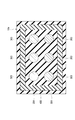
- 1 is a cross-sectional view of a semiconductor device according to a first embodiment of the present invention.
- 1 is a cross-sectional view of a semiconductor device according to a first embodiment of the present invention.
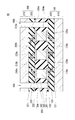
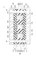
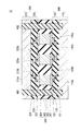
- 1 is a cross-sectional view of a semiconductor device according to a first embodiment of the present invention. It is sectional drawing of the semiconductor device of the 2nd Embodiment of this invention. It is sectional drawing of the semiconductor device of the 2nd Embodiment of this invention. It is sectional drawing of the semiconductor device of the 3rd Embodiment of this invention. It is sectional drawing of the semiconductor device of the 3rd Embodiment of this invention. It is sectional drawing of the semiconductor device of the 4th Embodiment of this invention.
- FIG. 1 shows a configuration of a semiconductor device 10 according to the first embodiment of the present invention.
- FIG. 1 shows a cross section of the semiconductor device 10.
- the semiconductor device 10 includes a first substrate 100, a second substrate 200, a first connection part 300, and an insulating layer 400.
- the first substrate 100 and the second substrate 200 are connected via the first connection portion 300.
- the first substrate 100 and the second substrate 200 are stacked in the thickness direction Dr1 of the first substrate 100.
- the thickness direction Dr1 of the first substrate 100 is a direction perpendicular to the surface 110a of the first semiconductor layer 110.
- the dimensions of the parts constituting the semiconductor device 10 do not follow the dimensions shown in FIG.
- the dimensions of the parts constituting the semiconductor device 10 may be arbitrary. The same applies to dimensions in cross-sectional views other than FIG.
- the first substrate 100 includes a first semiconductor layer 110 and a first wiring layer 120.
- the first semiconductor layer 110 and the first wiring layer 120 overlap with the thickness direction Dr1 of the first substrate 100.
- the first semiconductor layer 110 and the first wiring layer 120 are in contact with each other.
- the first semiconductor layer 110 is made of a first semiconductor material.
- the first semiconductor material is silicon (Si).
- the first semiconductor layer 110 has a surface 110a (first surface) and a surface 110b (second surface).
- the surface 110 a of the first semiconductor layer 110 constitutes one of the main surfaces of the first substrate 100.
- the main surface of the substrate is the widest surface among a plurality of surfaces constituting the surface of the substrate.
- the surface 110 b of the first semiconductor layer 110 is in contact with the first wiring layer 120.
- the first wiring layer 120 includes a first wiring 121, a first via 122, and a first interlayer insulating film 123.
- first wiring 121 there are a plurality of first wirings 121, but a symbol of one first wiring 121 is shown as a representative.
- first vias 122 there are a plurality of first vias 122, but a symbol of one first via 122 is shown as a representative.
- the first wiring layer 120 has a surface 120a (third surface) and a surface 120b (fourth surface).
- the surface 120 a of the first wiring layer 120 faces the surface 110 b of the first semiconductor layer 110.
- the surface 120 a of the first wiring layer 120 is in contact with the surface 110 b of the first semiconductor layer 110.
- the surface 120 b of the first wiring layer 120 constitutes one of the main surfaces of the first substrate 100.
- the surface 120 b of the first wiring layer 120 faces the second substrate 200.
- the surface 120 b of the first wiring layer 120 is in contact with the first connection part 300.
- the first wiring 121 and the first via 122 are made of a first conductive material.
- the first conductive material is a metal such as aluminum (Al) and copper (Cu).
- the first wiring 121 and the first via 122 may be made of different conductive materials.
- the first wiring 121 is a thin film on which a wiring pattern is formed.
- the first wiring 121 transmits a signal. Only one layer of the first wiring 121 may be disposed, or a plurality of layers of the first wiring 121 may be disposed. In the example shown in FIG. 1, two layers of the first wiring 121 are arranged.
- the first via 122 connects the first wirings 121 of different layers.
- portions other than the first wiring 121 and the first via 122 are constituted by the first interlayer insulating film 123.
- the first interlayer insulating film 123 is made of a first insulating material.
- the first insulating material is silicon dioxide (SiO2).
- At least one of the first semiconductor layer 110 and the first wiring layer 120 may include a circuit element such as a transistor.
- the first substrate 100 includes the first semiconductor layer 110 and the first wiring layer 120.
- the first semiconductor layer 110 has a surface 110a (first surface) and a surface 110b (second surface) and includes a first semiconductor material.
- the first wiring layer 120 includes a surface 120 a (third surface), a surface 120 b (fourth surface), and a first wiring 121, and the surface 120 a includes the surface 110 b of the first semiconductor layer 110. opposite.
- the second substrate 200 includes a second semiconductor layer 210 and a second wiring layer 220.
- the second semiconductor layer 210 and the second wiring layer 220 overlap with the thickness direction Dr1 of the first substrate 100.
- the second semiconductor layer 210 and the second wiring layer 220 are in contact with each other.
- the second semiconductor layer 210 is made of a second semiconductor material.
- the second semiconductor material is the same as the first semiconductor material constituting the first semiconductor layer 110.
- the second semiconductor material is different from the first semiconductor material.
- the second semiconductor material is silicon (Si).
- the second semiconductor layer 210 has a surface 210a (fifth surface) and a surface 210b (sixth surface).
- the surface 210 a of the second semiconductor layer 210 constitutes one of the main surfaces of the second substrate 200.
- the surface 210 b of the second semiconductor layer 210 is in contact with the second wiring layer 220.
- the second wiring layer 220 includes a second wiring 221, a second via 222, and a second interlayer insulating film 223.
- FIG. 1 there are a plurality of second wirings 221, but a symbol of one second wiring 221 is shown as a representative.
- FIG. 1 there are a plurality of second vias 222, but a symbol of one second via 222 is shown as a representative.
- the second wiring layer 220 has a surface 220a (seventh surface) and a surface 220b (eighth surface).
- the surface 220 a of the second wiring layer 220 faces the surface 210 b of the second semiconductor layer 210.
- the surface 220 a of the second wiring layer 220 is in contact with the surface 210 b of the second semiconductor layer 210.
- the surface 220 b of the second wiring layer 220 constitutes one of the main surfaces of the second substrate 200.
- the surface 220 b of the second wiring layer 220 faces the first substrate 100.
- the surface 220 b of the second wiring layer 220 is in contact with the first connection part 300.
- the second wiring 221 and the second via 222 are made of a second conductive material.
- the second conductive material is the same as the first conductive material constituting the first wiring 121 and the first via 122.
- the second conductive material is different from the first conductive material.
- the second conductive material is a metal such as aluminum (Al) and copper (Cu).
- the second wiring 221 and the second via 222 may be made of different conductive materials.
- the second wiring 221 is a thin film on which a wiring pattern is formed.
- the second wiring 221 transmits a signal. Only one layer of the second wiring 221 may be arranged, or a plurality of layers of the second wiring 221 may be arranged. In the example shown in FIG. 1, two layers of second wirings 221 are arranged.
- the second via 222 connects the second wirings 221 of different layers.
- portions other than the second wiring 221 and the second via 222 are configured by the second interlayer insulating film 223.
- the second interlayer insulating film 223 is made of a second insulating material.
- the second insulating material is the same as the first insulating material constituting the first interlayer insulating film 123.
- the second insulating material is different from the first insulating material.
- the second insulating material is silicon dioxide (SiO2).
- At least one of the second semiconductor layer 210 and the second wiring layer 220 may include a circuit element such as a transistor.
- the second substrate 200 includes the second semiconductor layer 210 and the second wiring layer 220.
- the second semiconductor layer 210 has a surface 210a (fifth surface) and a surface 210b (sixth surface) and includes a second semiconductor material.
- the second wiring layer 220 includes a surface 220 a (seventh surface), a surface 220 b (eighth surface), and a second wiring 221, and the surface 220 a includes the surface 210 b of the second semiconductor layer 210. opposite.
- the first substrate 100 and the second substrate 200 are arranged so that the first wiring layer 120 and the second wiring layer 220 face each other.
- the first connection unit 300 is disposed between the first wiring layer 120 and the second wiring layer 220.
- the first connection unit 300 electrically connects the first wiring 121 and the second wiring 221.
- the first connection unit 300 includes a first pad 301, a second pad 302, a first micro bump 303, and a first resin layer 304.
- first pads 301 there are a plurality of first pads 301, but a symbol of one first pad 301 is shown as a representative.
- there are a plurality of first micro bumps 303 but a symbol of one first micro bump 303 is shown as a representative.
- the first pad 301 is made of a conductive material.
- the conductive material constituting the first pad 301 is the first conductive material constituting the first wiring 121 and the first via 122 or the second wiring 221 constituting the first via 122 and the second via 222. The same as the conductive material.
- the conductive material forming the first pad 301 is different from the first conductive material or the second conductive material.
- the conductive material constituting the first pad 301 is a metal such as gold (Au), copper (Cu), or nickel (Ni).
- the first pad 301 is a thin film.
- the first pad 301 is disposed on the surface 120 b of the first wiring layer 120.
- the first pad 301 is in contact with the first via 122 on the surface 120 b of the first wiring layer 120. For this reason, the first pad 301 is electrically connected to the first wiring 121.
- the second pad 302 is made of a conductive material.
- the conductive material constituting the second pad 302 is the first conductive material constituting the first wiring 121 and the first via 122 or the second wiring 221 constituting the second via 222 and the second via 222. The same as the conductive material.
- the conductive material forming the second pad 302 is different from the first conductive material or the second conductive material.
- the conductive material constituting the second pad 302 is a metal such as gold (Au), copper (Cu), and nickel (Ni).
- the second pad 302 is a thin film.
- the second pad 302 is disposed on the surface 220 b of the second wiring layer 220.
- the second pad 302 is in contact with the second via 222 on the surface 220 b of the second wiring layer 220. For this reason, the second pad 302 is electrically connected to the second wiring 221.
- the first micro bump 303 is made of a conductive material.
- the conductive material constituting the first microbump 303 is the first conductive material constituting the first wiring 121 and the first via 122 or the second wiring 221 and the second via 222 constituting the second via 222. 2 is the same as the conductive material.
- the conductive material constituting the first microbump 303 is different from the first conductive material or the second conductive material.
- the conductive material constituting the first micro bump 303 is a metal such as gold (Au), copper (Cu), and nickel (Ni).
- the first micro bump 303 is a columnar structure.
- the first micro bump 303 may be a spherical structure.
- the first micro bump 303 is disposed between the first pad 301 and the second pad 302 and is electrically connected to the first pad 301 and the second pad 302. With the above structure, the first pad 301, the second pad 302, and the first micro bump 303 are electrically connected to the first wiring 121 and the second wiring 221, and the first A signal is transmitted between the substrate 100 and the second substrate 200.
- the first resin layer 304 is disposed between the first wiring layer 120 and the second wiring layer 220.
- the first resin layer 304 is made of a first resin material.
- the first resin material is an underfill resin.
- the first resin layer 304 covers the surfaces of the first pad 301, the second pad 302, and the first micro bump 303.
- the first pad 301 is disposed on the surface 120b (fourth surface) of the first wiring layer 120 and is electrically connected to the first wiring 121.
- the second pad 302 is disposed on the surface 220 b (eighth surface) of the second wiring layer 220 and is electrically connected to the second wiring 221.
- the first micro bump 303 is disposed between the first substrate 100 and the second substrate 200 and is electrically connected to the first pad 301 and the second pad 302.
- the first resin layer 304 is disposed between the first substrate 100 and the second substrate 200 and is in contact with the first pad 301, the second pad 302, and the first micro bump 303.
- the first resin layer 304 includes a first resin material.
- the insulating layer 400 penetrates the second substrate 200 and the first resin layer 304.
- the insulating layer 400 is in contact with the surface 120b of the first wiring layer 120.
- the insulating layer 400 includes an insulating material that is less hygroscopic than the first resin layer 304.
- the insulating material constituting the insulating layer 400 is silicon nitride (SiN), silicon dioxide (SiO 2), or the like.
- the hygroscopicity of the insulating layer 400 is indicated by the moisture absorption rate.
- the moisture absorption rate of the insulating layer 400 is smaller than the moisture absorption rate of the first resin layer 304.
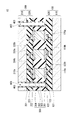
- FIG. 2 shows a first cross section 10a of the semiconductor device 10 at position A1 in FIG.
- the first cross section 10 a passes through the first micro bump 303, the first resin layer 304, and the insulating layer 400, and is parallel to the surface 110 a of the first semiconductor layer 110.
- the semiconductor device 10 includes a plurality of first micro bumps 303.
- the plurality of first micro bumps 303 are arranged in the circuit formation region including the central portion in the first cross section 10a.
- the plurality of first micro bumps 303 are arranged in a matrix.
- the cross-sectional shape of the first micro bump 303 is a circle.
- the cross-sectional shape of the first micro bump 303 may be a polygon.
- the insulating layer 400 is disposed so as to surround the plurality of first micro bumps 303. That is, in the first cross section 10 a, the plurality of first micro bumps 303 are surrounded by the insulating layer 400. In the first cross section 10a, the insulating layer 400 is unbroken.
- the insulating layer 400 includes an insulating material that is less hygroscopic than the first resin layer 304.
- the insulating layer 400 penetrates the second substrate 200 and the first resin layer 304.
- the insulating layer 400 is The first micro bump 303 is surrounded.
- the insulating layer 400 surrounds the first micro bump 303 in a cross section that passes through the first pad 301, the first resin layer 304, and the insulating layer 400 and is parallel to the surface 110 a of the first semiconductor layer 110. . Further, the insulating layer 400 surrounds the first micro bump 303 in a cross section that passes through the second pad 302, the first resin layer 304, and the insulating layer 400 and is parallel to the surface 110 a of the first semiconductor layer 110.
- the first resin layer 304 is exposed at the chip end of the semiconductor device 10. That is, the first resin layer 304 is in contact with the outside air at the chip end of the semiconductor device 10. Moisture in the outside air enters the first resin layer 304. Since the insulating layer 400 has low hygroscopicity, moisture hardly enters the insulating layer 400. In addition, since the insulating layer 400 penetrates the first resin layer 304, the path from the chip end to the first micro bump 303 is blocked by the insulating layer 400. For this reason, the moisture in the outside air that has entered the first resin layer 304 hardly reaches the first micro bumps 303. As a result, the semiconductor device 10 can reduce deformation of the first micro bump 303 due to moisture absorption of the first resin layer 304.
- FIG. 3 shows the semiconductor device 10 before the insulating layer 400 is formed.
- FIG. 3 shows a cross section of the semiconductor device 10.
- the second semiconductor layer 210, the second wiring layer 220, and the first resin layer 304 are dug down in order from the surface 210a side of the second semiconductor layer 210.
- the surface 120b of the first wiring layer 120 is exposed and a groove 900 is formed.
- the semiconductor device 10 has a groove 900.
- the groove 900 is formed across the second semiconductor layer 210, the second wiring layer 220, and the first resin layer 304.
- the groove 900 includes a side surface 210 c of the second semiconductor layer 210, a side surface 220 c of the second wiring layer 220, a side surface 304 a of the first resin layer 304, and a surface 120 b of the first wiring layer 120.
- the insulating layer 400 is formed. That is, the insulating layer 400 is disposed in the groove 900.
- the semiconductor device according to each aspect of the present invention may not have a configuration corresponding to at least one of the first via 122 and the second via 222.
- the semiconductor device 10 includes a first substrate 100, a second substrate 200, a first pad 301, a second pad 302, a first micro bump 303, The first resin layer 304 and the insulating layer 400 are included.
- the semiconductor device 10 can reduce deformation of the first micro bump 303 due to moisture absorption of the first resin layer 304.
- FIG. 4 shows the configuration of the semiconductor device 11 according to the second embodiment of the present invention.
- FIG. 4 shows a cross section of the semiconductor device 11.
- the semiconductor device 11 includes a first substrate 100, a second substrate 200, a first connection portion 300, and an insulating layer 401.
- the insulating layer 401 passes through the second substrate 200, the first resin layer 304, and the first wiring layer 120. A part of the insulating layer 401 is disposed inside the first substrate 100. The insulating layer 401 is in contact with the surface 110 b of the first semiconductor layer 110. The insulating layer 401 is made of an insulating material similar to the insulating material that forms the insulating layer 400.
- the arrangement of the components in the cross section passing through the first micro bump 303, the first resin layer 304, and the insulating layer 401 and parallel to the surface 110a of the first semiconductor layer 110 is the arrangement of the components shown in FIG. It is the same. That is, the insulating layer 401 is disposed so as to surround the plurality of first micro bumps 303.
- FIG. 5 shows the semiconductor device 11 before the insulating layer 401 is formed.
- FIG. 5 shows a cross section of the semiconductor device 11.
- the second semiconductor layer 210, the second wiring layer 220, the first resin layer 304, and the first wiring layer 120 are formed from the surface 210a side of the second semiconductor layer 210. And are dug down in order. As a result, the surface 110b of the first semiconductor layer 110 is exposed and a groove 901 is formed.
- the semiconductor device 11 has a groove 901. The groove 901 is formed across the second semiconductor layer 210, the second wiring layer 220, the first resin layer 304, and the first wiring layer 120.
- the groove 901 includes the side surface 210c of the second semiconductor layer 210, the side surface 220c of the second wiring layer 220, the side surface 304a of the first resin layer 304, the side surface 120c of the first wiring layer 120, and the first And the surface 110b of the semiconductor layer 110.
- the insulating layer 401 is formed by filling the groove 901 with an insulating material. That is, the insulating layer 401 is disposed in the groove 901.
- the groove 901 opens to the surface 120 a of the first wiring layer 120 and the surface 120 b of the first wiring layer 120. That is, the groove 901 constitutes an opening on the surface 120 a of the first wiring layer 120 and an opening on the surface 120 b of the first wiring layer 120.
- the groove 901 may be opened only on the surface 120 b of the first wiring layer 120. That is, the position of the bottom surface of the groove 901 may be between the surface 120 a of the first wiring layer 120 and the surface 120 b of the first wiring layer 120. In this case, the insulating layer 401 does not penetrate the first wiring layer 120 and reaches the inside of the first wiring layer 120.
- the semiconductor device 11 includes a first substrate 100, a second substrate 200, a first pad 301, a second pad 302, a first micro bump 303, A first resin layer 304 and an insulating layer 401 are included.
- the semiconductor device 11 can reduce deformation of the first micro bumps 303 due to moisture absorption of the first resin layer 304.
- the adhesive strength between the insulating layer 400 and the first wiring layer 120 may be low.
- moisture in the outside air that has entered the first resin layer 304 may enter the boundary between the insulating layer 400 and the first wiring layer 120. That is, moisture may travel along a path including the boundary between the insulating layer 400 and the first wiring layer 120.
- the path through which moisture is transmitted is the boundary between the insulating layer 401 and the first wiring layer 120 and the boundary between the insulating layer 401 and the first semiconductor layer 110. including. That is, in the semiconductor device 11 of the second embodiment, the path for moisture to be transmitted is longer than the path in the semiconductor device 10 of the first embodiment.
- the semiconductor device 11 can further reduce deformation of the first micro bumps 303 due to moisture absorption of the first resin layer 304.
- FIG. 6 shows the configuration of the semiconductor device 12 according to the third embodiment of the present invention.
- FIG. 6 shows a cross section of the semiconductor device 12.
- the semiconductor device 12 includes a first substrate 100, a second substrate 200, a first connection portion 300, and an insulating layer 402.
- the insulating layer 402 penetrates the second substrate 200, the first resin layer 304, and the first wiring layer 120. A part of the insulating layer 402 is disposed inside the first substrate 100 and the first semiconductor layer 110.
- the insulating layer 402 is made of an insulating material similar to the insulating material that forms the insulating layer 400.
- the arrangement of the components in a cross section passing through the first micro bump 303, the first resin layer 304, and the insulating layer 402 and parallel to the surface 110a of the first semiconductor layer 110 is the arrangement of the components shown in FIG. It is the same. That is, the insulating layer 402 is disposed so as to surround the plurality of first micro bumps 303.
- FIG. 7 shows the semiconductor device 12 before the insulating layer 402 is formed.
- FIG. 7 shows a cross section of the semiconductor device 12.
- the second semiconductor layer 210, the second wiring layer 220, the first resin layer 304, and the first wiring layer 120 are formed from the surface 210a side of the second semiconductor layer 210. Then, the first semiconductor layer 110 is dug down in order. As a result, the first semiconductor layer 110 is exposed and a groove 902 is formed.
- the semiconductor device 12 has a groove 902. The groove 902 is formed across the second semiconductor layer 210, the second wiring layer 220, the first resin layer 304, the first wiring layer 120, and the first semiconductor layer 110. .
- the groove 902 includes the side surface 210c of the second semiconductor layer 210, the side surface 220c of the second wiring layer 220, the side surface 304a of the first resin layer 304, the side surface 120c of the first wiring layer 120, and the first side.
- the side surface 110c of the semiconductor layer 110 and the surface 110d of the first semiconductor layer 110 are included.
- the insulating layer 402 is formed by filling the groove 902 with an insulating material. That is, the insulating layer 402 is disposed in the groove 902.
- the groove 902 opens to the surface 120 a of the first wiring layer 120 and the surface 120 b of the first wiring layer 120. That is, the groove 902 constitutes an opening on the surface 120 a of the first wiring layer 120 and an opening on the surface 120 b of the first wiring layer 120.
- the groove 902 is open to the surface 110 b of the first semiconductor layer 110. That is, the groove 902 forms an opening of the surface 110 b of the first semiconductor layer 110.
- the semiconductor device 11 includes a first substrate 100, a second substrate 200, a first pad 301, a second pad 302, a first micro bump 303, The first resin layer 304 and the insulating layer 402 are included.
- the semiconductor device 12 can reduce deformation of the first micro bumps 303 due to moisture absorption of the first resin layer 304.
- the path for moisture to be transmitted is longer than the path in the semiconductor device 11 of the second embodiment. For this reason, the moisture in the outside air that has entered the first resin layer 304 is unlikely to reach the first micro bumps 303. As a result, the semiconductor device 12 can further reduce deformation of the first micro bumps 303 due to moisture absorption of the first resin layer 304.
- FIG. 8 shows the configuration of the semiconductor device 13 according to the fourth embodiment of the present invention.
- FIG. 8 shows a cross section of the semiconductor device 13.
- the semiconductor device 13 includes a first substrate 100, a second substrate 200, a first connection portion 300, an insulating layer 403, and a metal layer 410.
- the insulating layer 403 penetrates the second substrate 200 and the first resin layer 304.
- the insulating layer 403 is in contact with the surface 120 b of the first wiring layer 120.
- the insulating layer 403 is made of an insulating material similar to the insulating material that forms the insulating layer 400.
- the metal layer 410 is disposed inside the insulating layer 403.
- the metal layer 410 penetrates the second substrate 200.
- a part of the metal layer 410 is disposed inside the first resin layer 304.
- the metal layer 410 is made of a metal material.
- the side surface and the bottom surface of the metal layer 410 are in contact with the insulating layer 403.
- the bottom surface of the metal layer 410 may contact the surface 120 b of the first wiring layer 120.
- the hygroscopicity of the metal layer 410 is lower than the hygroscopicity of the insulating layer 403. For this reason, even when moisture enters the insulating layer 403, the moisture hardly passes through the metal layer 410. That is, moisture in the outside air that has entered the first resin layer 304 hardly reaches the first micro bumps 303. As a result, the semiconductor device 13 can reduce deformation of the first micro bumps 303 due to moisture absorption of the first resin layer 304.
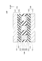
- FIG. 9 shows the first cross section 13a of the semiconductor device 13 at position A2 in FIG.
- the first cross section 13 a passes through the first micro bump 303, the first resin layer 304, the insulating layer 403, and the metal layer 410, and is parallel to the surface 110 a of the first semiconductor layer 110.
- the insulating layer 403 and the metal layer 410 are disposed so as to surround the plurality of first micro bumps 303. That is, in the first cross section 13 a, the plurality of first micro bumps 303 are surrounded by the insulating layer 403 and the metal layer 410. In the first cross section 13a, the insulating layer 403 and the metal layer 410 are unbroken. Since the metal layer 410 is surrounded by the insulating layer 403, the metal layer 410 does not affect a signal transmitted through the first connection unit 300.
- the insulating layer 403 is disposed so as to surround the metal layer 410. That is, the metal layer 410 is surrounded by the insulating layer 403 in the first cross section 13a.
- the metal layer 410 includes a metal material.
- the metal layer 410 penetrates the second substrate 200 and is disposed inside the first resin layer 304.
- the metal layer 410 surrounds the first micro bump 303.
- the insulating layer 403 surrounds the metal layer 410.
- the metal layer 410 surrounds the first micro bump 303 in a cross section that passes through the first pad 301, the first resin layer 304, and the insulating layer 403 and is parallel to the surface 110 a of the first semiconductor layer 110.
- the insulating layer 403 surrounds the metal layer 410.
- the metal layer 410 surrounds the first micro bump 303 in a cross section that passes through the second pad 302, the first resin layer 304, and the insulating layer 403 and is parallel to the surface 110a of the first semiconductor layer 110.
- the insulating layer 403 surrounds the metal layer 410.
- FIG. 10 shows the semiconductor device 13 before the metal layer 410 is formed.
- FIG. 10 shows a cross section of the semiconductor device 13.
- FIG. 10 shows the semiconductor device 13 after the insulating layer 403 is formed.
- the surface of the insulating layer 403 forms a groove 903.
- the metal layer 410 is formed by filling the groove 903 with a metal material. That is, the metal layer 410 is disposed in the groove 903.
- the semiconductor device 13 includes a first substrate 100, a second substrate 200, a first pad 301, a second pad 302, a first micro bump 303, The first resin layer 304, the insulating layer 403, and the metal layer 410 are included.
- the semiconductor device 13 can reduce deformation of the first micro bumps 303 due to moisture absorption of the first resin layer 304.
- the semiconductor device 13 can further reduce deformation of the first micro bumps 303 due to moisture absorption of the first resin layer 304.
- FIG. 11 shows a configuration of a semiconductor device 14 according to the fifth embodiment of the present invention.
- FIG. 11 shows a cross section of the semiconductor device 14.
- the semiconductor device 14 includes a first substrate 100, a second substrate 200, a first connection portion 300, an insulating layer 404, and a metal layer 411.
- the insulating layer 404 penetrates the second substrate 200, the first resin layer 304, and the first wiring layer 120. A part of the insulating layer 404 is disposed inside the first substrate 100. The insulating layer 404 is in contact with the surface 110 b of the first semiconductor layer 110.
- the insulating layer 404 is made of an insulating material similar to the insulating material that forms the insulating layer 400.
- the metal layer 411 penetrates the second substrate 200 and the first resin layer 304. A part of the metal layer 411 is disposed inside the first substrate 100 and the first wiring layer 120.
- the metal layer 411 is made of the same metal material as that of the metal layer 410.
- each component in a cross section passing through the first micro bump 303, the first resin layer 304, the insulating layer 404, and the metal layer 411 and parallel to the surface 110a of the first semiconductor layer 110 is shown in FIG. This is the same as the arrangement of each component. That is, the insulating layer 404 and the metal layer 411 are disposed so as to surround the plurality of first micro bumps 303. The insulating layer 404 is disposed so as to surround the metal layer 411.
- an insulating material adheres to the groove 901 so as to cover the surface of the groove 901.
- the insulating layer 404 is formed.
- a metal layer 411 is formed by filling a groove formed by the surface of the insulating layer 404 with a metal material.
- the semiconductor device 14 includes the first substrate 100, the second substrate 200, the first pad 301, the second pad 302, the first micro bump 303, The first resin layer 304, the insulating layer 404, and the metal layer 411 are included.
- the semiconductor device 14 can reduce deformation of the first micro bump 303 due to moisture absorption of the first resin layer 304.
- the semiconductor device 14 can further reduce deformation of the first micro bumps 303 due to moisture absorption of the first resin layer 304.
- the path through which moisture is transmitted is longer than the path in the semiconductor device 13 according to the fourth embodiment. For this reason, the moisture in the outside air that has entered the first resin layer 304 is unlikely to reach the first micro bumps 303. As a result, the semiconductor device 14 can further reduce deformation of the first micro bumps 303 due to moisture absorption of the first resin layer 304.
- FIG. 12 shows the configuration of the semiconductor device 15 according to the sixth embodiment of the present invention.
- FIG. 12 shows a cross section of the semiconductor device 15.
- the semiconductor device 15 includes a first substrate 100, a second substrate 200, a first connection portion 300, an insulating layer 405, and a metal layer 412.
- the insulating layer 405 passes through the second substrate 200, the first resin layer 304, and the first wiring layer 120. A part of the insulating layer 405 is disposed inside the first substrate 100 and the first semiconductor layer 110.
- the insulating layer 405 is made of an insulating material similar to the insulating material that forms the insulating layer 400.
- the metal layer 412 penetrates the second substrate 200, the first resin layer 304, and the first wiring layer 120. A part of the metal layer 412 is disposed inside the first substrate 100 and the first semiconductor layer 110.
- the metal layer 412 is made of a metal material similar to the metal material that forms the metal layer 410.
- each component in the cross section passing through the first micro bump 303, the first resin layer 304, the insulating layer 405, and the metal layer 412 and parallel to the surface 110a of the first semiconductor layer 110 is shown in FIG. This is the same as the arrangement of each component. That is, the insulating layer 405 and the metal layer 412 are disposed so as to surround the plurality of first micro bumps 303. The insulating layer 405 is disposed so as to surround the metal layer 412.
- an insulating material adheres to the groove 902 so as to cover the surface of the groove 902. Thereby, the insulating layer 405 is formed.
- a metal layer 412 is formed by filling a groove formed by the surface of the insulating layer 405 with a metal material.
- the semiconductor device 15 includes a first substrate 100, a second substrate 200, a first pad 301, a second pad 302, a first micro bump 303, The first resin layer 304, the insulating layer 405, and the metal layer 412 are included.
- the semiconductor device 15 can reduce deformation of the first micro bumps 303 due to moisture absorption of the first resin layer 304.
- the semiconductor device 15 can further reduce deformation of the first micro bumps 303 due to moisture absorption of the first resin layer 304.
- the path for moisture to be transmitted is longer than the path in the semiconductor device 14 of the fifth embodiment. For this reason, the moisture in the outside air that has entered the first resin layer 304 is unlikely to reach the first micro bumps 303. As a result, the semiconductor device 15 can further reduce deformation of the first micro bumps 303 due to moisture absorption of the first resin layer 304.
- FIG. 13 shows the configuration of the semiconductor device 16 according to the seventh embodiment of the present invention.
- FIG. 13 shows a cross section of the semiconductor device 16.
- the semiconductor device 16 includes a first substrate 100, a second substrate 200, a first connection portion 300, and an insulating layer 400.
- the insulating layer 400 is disposed at the end (chip end) of the semiconductor device 16. That is, the insulating layer 400 includes the end portion of the semiconductor device 16. For this reason, the side surface 400a of the insulating layer 400 is exposed.
- each semiconductor device 10 is completed by cutting the substrate at the end portion of the semiconductor device 10.
- the structure such as the first resin layer 304 is disposed outside the insulating layer 400.
- the semiconductor device 16 since the insulating layer 400 is disposed at the end of the semiconductor device 16, a structure outside the insulating layer 400 is not necessary. For this reason, the area of the semiconductor device 16 is reduced. As a result, in the semiconductor device 16, the number of semiconductor devices that can be acquired per unit area of the substrate is increased as compared with the semiconductor device 10.
- the lateral width of the semiconductor device 16 is substantially the same as the lateral width of the semiconductor device 10. However, the lateral width of the semiconductor device 16 can be made smaller than the lateral width of the semiconductor device 10 by reducing the distance between the insulating layer 400 and the first micro bump 303.
- an insulating layer 401 shown in FIG. instead of the insulating layer 400, an insulating layer 401 shown in FIG. Instead of the insulating layer 400, an insulating layer 402 shown in FIG. Instead of the insulating layer 400, an insulating layer 403 and a metal layer 410 shown in FIG. Instead of the insulating layer 400, an insulating layer 404 and a metal layer 411 shown in FIG. Instead of the insulating layer 400, an insulating layer 405 and a metal layer 412 shown in FIG.
- the semiconductor device 16 includes a first substrate 100, a second substrate 200, a first pad 301, a second pad 302, a first micro bump 303, The first resin layer 304 and the insulating layer 400 are included.
- the semiconductor device 16 can reduce deformation of the first micro bumps 303 due to moisture absorption of the first resin layer 304.
- FIG. 14 shows a configuration of a semiconductor device 17 according to the eighth embodiment of the present invention.
- FIG. 14 shows a cross section of the semiconductor device 17.
- the semiconductor device 17 includes a first substrate 100, a second substrate 201, a first connection portion 300, and an insulating layer 400.
- the first substrate 100 and the second substrate 201 are connected via the first connection unit 300.
- the first substrate 100 and the second substrate 201 are stacked in the thickness direction Dr1 of the first substrate 100.
- the second substrate 201 includes a second semiconductor layer 211 and a second wiring layer 220.
- the second semiconductor layer 211 and the second wiring layer 220 overlap with the thickness direction Dr1 of the first substrate 100.
- the second semiconductor layer 211 and the second wiring layer 220 are in contact with each other.
- the second semiconductor layer 211 is made of the same second semiconductor material as the second semiconductor material that constitutes the second semiconductor layer 210.
- the second semiconductor layer 211 has a surface 211a (fifth surface) and a surface 211b (sixth surface).
- the surface 211 a of the second semiconductor layer 211 constitutes one of the main surfaces of the second substrate 201.
- the surface 211 a of the second semiconductor layer 211 faces the first substrate 100.
- the surface 211 a of the second semiconductor layer 211 is in contact with the first connection part 300.
- the surface 211 b of the second semiconductor layer 211 is in contact with the second wiring layer 220.
- the second semiconductor layer 211 has a second through via 212.
- FIG. 14 there are a plurality of second through vias 212, but a symbol of one second through via 212 is shown as a representative.
- the second through via 212 penetrates the second semiconductor layer 211.
- the second through via 212 is in contact with the second via 222 on the surface 220 a of the second wiring layer 220. For this reason, the second through via 212 is electrically connected to the second wiring 221.
- the second through via 212 is in contact with the second pad 302 on the surface 211 a of the second semiconductor layer 211.
- the surface 220 a of the second wiring layer 220 faces the surface 211 b of the second semiconductor layer 211.
- the surface 220 a of the second wiring layer 220 is in contact with the surface 211 b of the second semiconductor layer 211.
- the surface 220 b of the second wiring layer 220 constitutes one of the main surfaces of the second substrate 201.
- At least one of the second semiconductor layer 211 and the second wiring layer 220 may include a circuit element such as a transistor.
- the first substrate 100 and the second substrate 201 are arranged so that the first wiring layer 120 and the second semiconductor layer 211 face each other.
- the first connection unit 300 is disposed between the first wiring layer 120 and the second semiconductor layer 211.
- the second pad 302 is disposed on the surface 211 a of the second semiconductor layer 211.
- the second pad 302 is in contact with the second through via 212 on the surface 211 a of the second semiconductor layer 211. For this reason, the second pad 302 is electrically connected to the second wiring 221.
- the second semiconductor layer 211 has the second through via 212 that penetrates the second semiconductor layer 211.
- the second pad 302 is disposed on the surface 211 a (fifth surface) of the second semiconductor layer 211 and is electrically connected to the second wiring 221 through the second through via 212. .
- an insulating layer 401 shown in FIG. instead of the insulating layer 400, an insulating layer 401 shown in FIG. Instead of the insulating layer 400, an insulating layer 402 shown in FIG. Instead of the insulating layer 400, an insulating layer 403 and a metal layer 410 shown in FIG. Instead of the insulating layer 400, an insulating layer 404 and a metal layer 411 shown in FIG. Instead of the insulating layer 400, an insulating layer 405 and a metal layer 412 shown in FIG.
- the second pad 302 is disposed on the surface 220 b of the second wiring layer 220.
- the second pad 302 is disposed on the surface 211 a of the second semiconductor layer 211. Therefore, in the semiconductor device according to each aspect of the present invention, the second pad may be disposed on the fifth surface of the second semiconductor layer or the eighth surface of the second wiring layer.
- the semiconductor device of each aspect of the present invention may not have a configuration corresponding to the second through via 212.
- the semiconductor device 17 includes a first substrate 100, a second substrate 201, a first pad 301, a second pad 302, a first micro bump 303, The first resin layer 304 and the insulating layer 400 are included.
- the semiconductor device 17 can reduce deformation of the first micro bumps 303 due to moisture absorption of the first resin layer 304.
- FIG. 15 shows a configuration of a semiconductor device 18 according to the ninth embodiment of the present invention.
- FIG. 15 shows a cross section of the semiconductor device 18.
- the semiconductor device 18 includes a first substrate 101, a second substrate 200, a first connection portion 300, and an insulating layer 400.
- the first substrate 101 and the second substrate 200 are connected via the first connection portion 300.
- the first substrate 101 and the second substrate 200 are stacked in the thickness direction Dr1 of the first substrate 101.
- the first substrate 101 includes a first semiconductor layer 111 and a first wiring layer 120.
- the first semiconductor layer 111 and the first wiring layer 120 overlap with the thickness direction Dr1 of the first substrate 101.
- the first semiconductor layer 111 and the first wiring layer 120 are in contact with each other.
- the first semiconductor layer 111 is made of the same first semiconductor material as the first semiconductor material constituting the first semiconductor layer 110.
- the first semiconductor layer 111 has a surface 111a (first surface) and a surface 111b (second surface).
- the surface 111 a of the first semiconductor layer 111 constitutes one of the main surfaces of the first substrate 101.
- the surface 111 a of the first semiconductor layer 111 faces the second substrate 200.
- the surface 111 a of the first semiconductor layer 111 is in contact with the first connection part 300.
- the surface 111 b of the first semiconductor layer 111 is in contact with the first wiring layer 120.
- the first semiconductor layer 111 has a first through via 112.
- first through vias 112 there are a plurality of first through vias 112, but a symbol of one first through via 112 is shown as a representative.
- the first through via 112 penetrates the first semiconductor layer 111.
- the first through via 112 is in contact with the first via 122 on the surface 120 a of the first wiring layer 120. For this reason, the first through via 112 is electrically connected to the first wiring 121.
- the first through via 112 is in contact with the first pad 301 on the surface 111 a of the first semiconductor layer 111.
- the surface 120 a of the first wiring layer 120 faces the surface 111 b of the first semiconductor layer 111.
- the surface 120 a of the first wiring layer 120 is in contact with the surface 111 b of the first semiconductor layer 111.
- the surface 120 b of the first wiring layer 120 constitutes one of the main surfaces of the first substrate 101.
- At least one of the first semiconductor layer 111 and the first wiring layer 120 may include a circuit element such as a transistor.
- the first substrate 101 and the second substrate 200 are arranged so that the first semiconductor layer 111 and the second wiring layer 220 face each other.
- the first connection unit 300 is disposed between the first semiconductor layer 111 and the second wiring layer 220.
- the first pad 301 is disposed on the surface 111 a of the first semiconductor layer 111.
- the first pad 301 is in contact with the first through via 112 on the surface 111 a of the first semiconductor layer 111. For this reason, the first pad 301 is electrically connected to the first wiring 121.
- the first semiconductor layer 111 has the first through via 112 that penetrates the first semiconductor layer 111.
- the first pad 301 is disposed on the surface 111 a (first surface) of the first semiconductor layer 111 and is electrically connected to the first wiring 121 through the first through via 112. .
- an insulating layer 401 shown in FIG. instead of the insulating layer 400, an insulating layer 401 shown in FIG. Instead of the insulating layer 400, an insulating layer 402 shown in FIG. Instead of the insulating layer 400, an insulating layer 403 and a metal layer 410 shown in FIG. Instead of the insulating layer 400, an insulating layer 404 and a metal layer 411 shown in FIG. Instead of the insulating layer 400, an insulating layer 405 and a metal layer 412 shown in FIG.
- the groove 901 in which the insulating layer 401 is disposed is the first wiring layer.
- the surface 120b of 120 is opened.
- the semiconductor device 18 when the insulating layer 401 shown in FIG. 4 is disposed and the first pad 301 is disposed on the surface 111 a (first surface) of the first semiconductor layer 111, the insulating layer 401. Is disposed in the surface 111 a of the first semiconductor layer 111.
- the insulating layer 400 may be disposed at the end of the semiconductor device 18. Instead of the second substrate 200, a second substrate 201 shown in FIG.
- the first pad 301 is disposed on the surface 120 b of the first wiring layer 120.
- the first pad 301 is disposed on the surface 111 a of the first semiconductor layer 111. Therefore, in the semiconductor device of each aspect of the present invention, the first pad may be disposed on the first surface of the first semiconductor layer or the fourth surface of the first wiring layer.
- the semiconductor device according to each aspect of the present invention may not have a configuration corresponding to the first through via 112.
- the semiconductor device 18 includes a first substrate 101, a second substrate 200, a first pad 301, a second pad 302, a first micro bump 303, The first resin layer 304 and the insulating layer 400 are included.
- the semiconductor device 18 can reduce deformation of the first micro bumps 303 due to moisture absorption of the first resin layer 304.
- FIG. 16 shows a configuration of a semiconductor device 19 according to the tenth embodiment of the present invention.
- FIG. 16 shows a cross section of the semiconductor device 19.
- the semiconductor device 19 includes a first substrate 100, a second substrate 202, a first connection portion 300, an insulating layer 406, a third substrate 500, and a second connection portion 600.
- the first substrate 100 and the second substrate 202 are connected via the first connection unit 300.
- the first substrate 100 and the second substrate 202 are stacked in the thickness direction Dr1 of the first substrate 100.
- the second substrate 202 and the third substrate 500 are connected via the second connection portion 600.
- the second substrate 202 and the third substrate 500 are stacked in the thickness direction Dr1 of the first substrate 100.
- the second substrate 202 includes a second semiconductor layer 211 and a second wiring layer 220.
- the arrangement of the second semiconductor layer 211 and the second wiring layer 220 is different from the arrangement of the second semiconductor layer 211 and the second wiring layer 220 in FIG. 14.
- the surface 211 a of the second semiconductor layer 211 faces the third substrate 500.
- the surface 211 a of the second semiconductor layer 211 is in contact with the second connection portion 600.
- the surface 211 b of the second semiconductor layer 211 is in contact with the second wiring layer 220.
- the first substrate 100 and the second substrate 202 are arranged so that the first wiring layer 120 and the second wiring layer 220 face each other.
- the third substrate 500 includes a third semiconductor layer 510 and a third wiring layer 520.
- the third semiconductor layer 510 and the third wiring layer 520 overlap with the thickness direction Dr1 of the first substrate 100. Further, the third semiconductor layer 510 and the third wiring layer 520 are in contact with each other.
- the third semiconductor layer 510 is made of a third semiconductor material.
- the third semiconductor material is the same as the first semiconductor material constituting the first semiconductor layer 110 or the second semiconductor material constituting the second semiconductor layer 210.
- the third semiconductor material is different from the first semiconductor material and the second semiconductor material.
- the third semiconductor material is silicon (Si).
- the third semiconductor layer 510 has a surface 510a (a ninth surface) and a surface 510b (a second surface).
- the surface 510 a of the third semiconductor layer 510 constitutes one of the main surfaces of the third substrate 500.
- a surface 510 a of the third semiconductor layer 510 faces the second substrate 202.
- the surface 510 a of the third semiconductor layer 510 is in contact with the second connection portion 600.
- the surface 510 b of the third semiconductor layer 510 is in contact with the third wiring layer 520.
- the third semiconductor layer 510 has a third through via 512.
- FIG. 16 there are a plurality of third through vias 512, but a symbol of one third through via 512 is shown as a representative.
- the third through via 512 penetrates the third semiconductor layer 510.
- the third through via 512 is in contact with the third via 522 on the surface 520 a of the third wiring layer 520. For this reason, the third through via 512 is electrically connected to the third wiring 521.
- the third through via 512 is in contact with the fourth pad 602 on the surface 510 a of the third semiconductor layer 510.
- the third wiring layer 520 includes a third wiring 521, a third via 522, and a third interlayer insulating film 523.
- a third wiring 521 there are a plurality of third wirings 521, but a symbol of one third wiring 521 is shown as a representative.
- a plurality of third vias 522 there are a plurality of third vias 522, but a symbol of one third via 522 is shown as a representative.
- the third wiring layer 520 has a surface 520a (11th surface) and a surface 520b (12th surface).
- the surface 520a of the third wiring layer 520 faces the surface 510b of the third semiconductor layer 510.
- the surface 520 a of the third wiring layer 520 is in contact with the surface 510 b of the third semiconductor layer 510.
- the surface 520 b of the third wiring layer 520 constitutes one of the main surfaces of the third substrate 500.
- the third wiring 521 and the third via 522 are made of a third conductive material.
- the third conductive material is the same as the first conductive material constituting the first wiring 121 and the first via 122 or the second conductive material constituting the second wiring 221 and the second via 222. It is. Alternatively, the third conductive material is different from the first conductive material and the second conductive material.
- the third conductive material is a metal such as aluminum (Al) and copper (Cu).
- the third wiring 521 and the third via 522 may be made of different conductive materials.
- the third wiring 521 is a thin film on which a wiring pattern is formed. The third wiring 521 transmits a signal. Only one layer of the third wiring 521 may be disposed, or a plurality of layers of the third wiring 521 may be disposed. In the example shown in FIG. 16, two layers of third wirings 521 are arranged.
- the third via 522 connects the third wirings 521 of different layers.
- portions other than the third wiring 521 and the third via 522 are configured by a third interlayer insulating film 523.
- the third interlayer insulating film 523 is made of a third insulating material.
- the third insulating material is the same as the first insulating material constituting the first interlayer insulating film 123 or the second insulating material constituting the second interlayer insulating film 223.
- the third insulating material is different from the first insulating material and the second insulating material.
- the third insulating material is silicon dioxide (SiO2).
- At least one of the third semiconductor layer 510 and the third wiring layer 520 may include a circuit element such as a transistor.
- the third substrate 500 includes the third semiconductor layer 510 and the third wiring layer 520.
- the third semiconductor layer 510 has a surface 510a (a ninth surface) and a surface 510b (a tenth surface), and includes a third semiconductor material.
- the third wiring layer 520 includes a surface 520a (an eleventh surface), a surface 520b (a twelfth surface), and a third wiring 521, and the surface 520a includes the surface 510b of the third semiconductor layer 510. opposite.
- the second substrate 202 and the third substrate 500 are arranged so that the second semiconductor layer 211 and the third semiconductor layer 510 face each other.
- the second connection portion 600 is disposed between the second semiconductor layer 211 and the third semiconductor layer 510.
- the second connection portion 600 electrically connects the second wiring 221 and the third wiring 521.
- the second connection portion 600 includes a third pad 601, a fourth pad 602, a second micro bump 603, and a second resin layer 604.
- there are a plurality of second micro bumps 603, but a symbol of one second micro bump 603 is shown as a representative.
- the third pad 601 is made of a conductive material.
- the conductive material constituting the third pad 601 is the first conductive material constituting the first wiring 121 and the first via 122, and the second conductive material constituting the second wiring 221 and the second via 222. , And any one of the third conductive material constituting the third wiring 521 and the third via 522.
- the conductive material constituting the third pad 601 is different from the first conductive material, the second conductive material, and the third conductive material.
- the conductive material constituting the third pad 601 is a metal such as gold (Au), copper (Cu), and nickel (Ni).
- the third pad 601 is a thin film.
- the third pad 601 is disposed on the surface 211 a of the second semiconductor layer 211.
- the third pad 601 is in contact with the second through via 212 on the surface 211 a of the second semiconductor layer 211. For this reason, the third pad 601 is electrically connected to the second wiring 221.
- the fourth pad 602 is made of a conductive material.
- the conductive material composing the fourth pad 602 is the first conductive material composing the first wiring 121 and the first via 122, and the second composing the second wiring 221 and the second via 222. , And any one of the third conductive material constituting the third wiring 521 and the third via 522.
- the conductive material constituting the fourth pad 602 is different from the first conductive material, the second conductive material, and the third conductive material.
- the conductive material constituting the fourth pad 602 is a metal such as gold (Au), copper (Cu), and nickel (Ni).
- the fourth pad 602 is a thin film.
- the fourth pad 602 is disposed on the surface 510 a of the third semiconductor layer 510.
- the fourth pad 602 is in contact with the third through via 512 on the surface 510 a of the third semiconductor layer 510. For this reason, the fourth pad 602 is electrically connected to the third wiring 521.
- the second micro bump 603 is made of a conductive material.
- the conductive material constituting the second microbump 603 is the first conductive material constituting the first wiring 121 and the first via 122, and the second wiring 221 and the second via 222 constituting the first via 122. 2 and the third conductive material constituting the third wiring 521 and the third via 522 are the same.
- the conductive material constituting the second microbump 603 is different from the first conductive material, the second conductive material, and the third conductive material.
- the conductive material constituting the second micro bump 603 is a metal such as gold (Au), copper (Cu), and nickel (Ni).
- the second micro bump 603 is a columnar structure.
- the second micro bump 603 may be a spherical structure.
- the second micro bump 603 is disposed between the third pad 601 and the fourth pad 602 and is electrically connected to the third pad 601 and the fourth pad 602.
- the third pad 601, the fourth pad 602, and the second micro bump 603 are electrically connected to the second wiring 221 and the third wiring 521, and the second pad A signal is transmitted between the substrate 202 and the third substrate 500.
- the second resin layer 604 is disposed between the second semiconductor layer 211 and the third semiconductor layer 510.
- the second resin layer 604 is made of a second resin material.
- the second resin material is the same as the first resin material constituting the first resin layer 304.
- the second resin material is different from the first resin material.
- the first resin material is an underfill resin.
- the second resin layer 604 covers the surfaces of the third pad 601, the fourth pad 602, and the second micro bump 603.
- the third pad 601 is disposed on the surface 211 a (fifth surface) of the second semiconductor layer 211 and is electrically connected to the second wiring 221.
- the fourth pad 602 is disposed on the surface 510 a (the ninth surface) of the third semiconductor layer 510 and is electrically connected to the third wiring 521.
- the second micro bump 603 is disposed between the second substrate 202 and the third substrate 500 and is electrically connected to the third pad 601 and the fourth pad 602.
- the second resin layer 604 is disposed between the second substrate 202 and the third substrate 500 and is in contact with the third pad 601, the fourth pad 602, and the second micro bump 603.
- the second resin layer 604 includes a second resin material.
- the insulating layer 406 penetrates the third substrate 500, the second substrate 200, and the first resin layer 304.
- the insulating layer 406 is made of an insulating material similar to the insulating material that forms the insulating layer 400.
- the insulating layer 406 includes an insulating material that has lower hygroscopicity than the first resin layer 304 and the second resin layer 604.
- the moisture absorption rate of the insulating layer 406 is smaller than the moisture absorption rate of the first resin layer 304 and the moisture absorption rate of the second resin layer 604.
- FIG. 16 is the same as the configuration shown in FIG. 1 or FIG.
- FIG. 17 shows a second cross section 19a of the semiconductor device 19 at position A3 in FIG.
- the second cross section 19 a passes through the second micro bump 603, the second resin layer 604, and the insulating layer 406 and is parallel to the surface 110 a of the first semiconductor layer 110.
- the semiconductor device 19 includes a plurality of second micro bumps 603.
- the plurality of second micro bumps 603 are arranged in the circuit formation region including the central portion in the second cross section 19a.
- the plurality of second micro bumps 603 are arranged in a matrix.
- the cross-sectional shape of the second micro bump 603 is a circle.
- the cross-sectional shape of the second micro bump 603 may be a polygon.
- the insulating layer 406 is disposed so as to surround the plurality of second micro bumps 603. That is, in the second cross section 19 a, the plurality of second micro bumps 603 are surrounded by the insulating layer 406. In the second cross section 19a, the insulating layer 406 is not cut.
- the insulating layer 406 includes an insulating material having lower hygroscopicity than the first resin layer 304 and the second resin layer 604.
- the insulating layer 406 penetrates the third substrate 500, the second substrate 200, and the first resin layer 304.
- the insulating layer 406 is The second micro bump 603 is surrounded.
- the insulating layer 406 surrounds the second micro bump 603 in a cross section that passes through the third pad 601, the second resin layer 604, and the insulating layer 406 and is parallel to the surface 110 a of the first semiconductor layer 110. . Further, the insulating layer 406 surrounds the second micro bump 603 in a cross section that passes through the fourth pad 602, the second resin layer 604, and the insulating layer 406 and is parallel to the surface 110 a of the first semiconductor layer 110.
- the second resin layer 604 is exposed at the chip end of the semiconductor device 19. That is, the second resin layer 604 is exposed to the outside air at the chip end of the semiconductor device 19. Moisture in the outside air enters the second resin layer 604. Since the insulating layer 406 has low hygroscopicity, moisture hardly enters the insulating layer 406. Further, since the insulating layer 406 penetrates the second resin layer 604, the path from the chip end to the second micro bump 603 is blocked by the insulating layer 406. For this reason, moisture in the outside air that has entered the second resin layer 604 hardly reaches the second micro bumps 603. As a result, the semiconductor device 19 can reduce deformation of the second micro bumps 603 due to moisture absorption of the second resin layer 604.
- FIG. 18 shows the semiconductor device 19 before the insulating layer 406 is formed.
- FIG. 18 shows a cross section of the semiconductor device 19.
- the third wiring layer 520, the third semiconductor layer 510, the second resin layer 604, and the second semiconductor layer 211 are formed from the surface 520b side of the third wiring layer 520. Then, the second wiring layer 220 and the first resin layer 304 are dug in order. As a result, the surface 120b of the first wiring layer 120 is exposed and a groove 904 is formed.
- the semiconductor device 19 has a groove 904.
- the groove 904 includes a third wiring layer 520, a third semiconductor layer 510, a second resin layer 604, a second semiconductor layer 211, a second wiring layer 220, and a first resin layer 304. And is formed over.
- the groove 904 includes a side surface 520c of the third wiring layer 520, a side surface 510c of the third semiconductor layer 510, a side surface 604a of the second resin layer 604, a side surface 211c of the second semiconductor layer 211, and a second surface.
- the side surface 220c of the wiring layer 220, the side surface 304a of the first resin layer 304, and the surface 120b of the first wiring layer 120 are included.
- the insulating layer 406 is formed. That is, the insulating layer 406 is disposed in the groove 904.
- the insulating layer 406 may penetrate the first wiring layer 120.
- a metal layer may be disposed inside the insulating layer 406.
- the insulating layer 406 may be disposed at the end portion of the semiconductor device 19. Instead of the first substrate 100, a first substrate 101 shown in FIG.
- the second pad 302 is disposed on the surface 220b (eighth surface) of the second wiring layer 220, and the third pad 601 is the surface 211a (first surface) of the second semiconductor layer 211. 5 plane).
- the second semiconductor layer 211 may be in contact with the first connection part 300, and the second wiring layer 220 may be in contact with the second connection part 600.
- the second pad 302 is disposed on the surface 211a (fifth surface) of the second semiconductor layer 211, and the third pad 601 is the surface 220b (eighth surface) of the second wiring layer 220. Placed in.
- the third pad may be disposed on the eighth surface of the second wiring layer or the fifth surface of the second semiconductor layer.
- the third pad is disposed on the eighth surface of the second wiring layer.
- the third pad is disposed on the fifth surface of the second semiconductor layer.
- the fourth pad 602 is disposed on the surface 510 a (the ninth surface) of the third semiconductor layer 510.
- the positional relationship between the third semiconductor layer 510 and the third wiring layer 520 may be reversed. That is, the third wiring layer 520 may be in contact with the first connection unit 300.
- the fourth pad 602 is disposed on the surface 520b (the twelfth surface) of the third wiring layer 520. Therefore, in the semiconductor device according to each aspect of the present invention, the fourth pad may be disposed on the ninth surface of the third semiconductor layer or the twelfth surface of the third wiring layer.
- the semiconductor device according to each aspect of the present invention may not have a configuration corresponding to at least one of the third through via 512 and the third via 522.
- the semiconductor device of each aspect of the present invention may include four or more substrates and three or more connection portions.
- the semiconductor devices are the semiconductor device 10, the semiconductor device 11, the semiconductor device 12, the semiconductor device 13, the semiconductor device 14, the semiconductor device 15, the semiconductor device 16, the semiconductor device 17, and the semiconductor.
- a structure similar to any one of the structures with the device 18 is included.
- the semiconductor device may include a structure similar to that of the semiconductor device 19.
- the semiconductor device 19 includes a first substrate 100, a second substrate 202, a first pad 301, a second pad 302, a first micro bump 303, A first resin layer 304 and an insulating layer 406 are provided. Further, the semiconductor device 19 includes a third substrate 500, a third pad 601, a fourth pad 602, a second micro bump 603, and a second resin layer 604.
- the semiconductor device 19 can reduce deformation of the first micro bumps 303 due to moisture absorption of the first resin layer 304.
- the semiconductor device 19 can reduce deformation of the second micro bumps 603 due to moisture absorption of the second resin layer 604.
- FIG. 19 shows the configuration of the semiconductor device 20 according to the eleventh embodiment of the present invention.
- FIG. 19 shows a cross section of the semiconductor device 20.
- the semiconductor device 20 includes a first substrate 100, a second substrate 203, a first connection portion 300, an insulating layer 400, a microlens ML, and a color filter CF.
- the first substrate 100 and the second substrate 203 are connected via the first connection portion 300.
- the first substrate 100 and the second substrate 203 are stacked in the thickness direction Dr1 of the first substrate 100.
- the semiconductor device 20 is a solid-state imaging device.
- the second substrate 203 includes a second semiconductor layer 213 and a second wiring layer 220.
- the second semiconductor layer 213 and the second wiring layer 220 overlap with the thickness direction Dr1 of the first substrate 100.
- the second semiconductor layer 213 and the second wiring layer 220 are in contact with each other.
- the second semiconductor layer 213 is made of the same second semiconductor material as the second semiconductor material constituting the second semiconductor layer 210.
- the second semiconductor layer 213 has a surface 213a (fifth surface) and a surface 213b (sixth surface).
- the surface 213 a of the second semiconductor layer 213 constitutes one of the main surfaces of the second substrate 200.
- the surface 213a of the second semiconductor layer 213 is in contact with the color filter CF.
- the surface 213 b of the second semiconductor layer 213 is in contact with the second wiring layer 220.
- the second semiconductor layer 213 includes a photoelectric conversion unit 214.
- the photoelectric conversion unit 214 is made of a semiconductor material having an impurity concentration different from that of the second semiconductor material forming the second semiconductor layer 213.
- the color filter CF is disposed on the surface 213a of the second semiconductor layer 213.
- a microlens ML is disposed on the color filter CF.
- the light from the subject that has passed through the imaging lens disposed optically in front of the semiconductor device 20 enters the microlens ML.
- the micro lens ML forms an image of light that has passed through the imaging lens.
- the color filter CF transmits light having a wavelength corresponding to a predetermined color.
- the light transmitted through the microlens ML and the color filter CF is incident on the second semiconductor layer 213.
- the light incident on the second semiconductor layer 213 travels through the second semiconductor layer 213 and enters the photoelectric conversion unit 214.
- the photoelectric conversion unit 214 converts incident light into a signal.
- the semiconductor device 20 can reduce deformation of the first micro bumps 303 due to moisture absorption of the first resin layer 304.
- the semiconductor device can reduce the deformation of the micro bump due to moisture absorption of the resin layer.
Landscapes
- Internal Circuitry In Semiconductor Integrated Circuit Devices (AREA)
- Structures Or Materials For Encapsulating Or Coating Semiconductor Devices Or Solid State Devices (AREA)
Abstract
半導体装置は、第1の基板と、第2の基板と、第1のパッドと、第2のパッドと、第1のマイクロバンプと、第1の樹脂層と、絶縁層とを有する。前記第1の基板は、第1の半導体層と第1の配線層とを有する。前記第2の基板は、第2の半導体層と第2の配線層とを有する。前記絶縁層は、前記第1の樹脂層よりも吸湿性が低い絶縁材料を含む。前記絶縁層は、前記第2の基板と前記第1の樹脂層とを貫通する。前記第1のマイクロバンプと前記第1の樹脂層と前記絶縁層とを通り、かつ前記第1の面に平行な第1の断面において、前記絶縁層は前記第1のマイクロバンプを囲む。
Description
本発明は、半導体装置に関する。
複数の積層された基板を有する半導体装置が開示されている(例えば、特許文献1)。図20は、複数の基板を有する半導体装置1010の構成を示している。図20では半導体装置1010の断面が示されている。図20に示すように、半導体装置1010は、第1の基板1100と、第2の基板1200と、接続部1300とを有する。第1の基板1100と第2の基板1200とは、接続部1300を介して接続されている。第1の基板1100と第2の基板1200とは、第1の基板1100の厚さ方向Dr1001に積層されている。
第1の基板1100は、第1の半導体層1110と、第1の配線層1120とを有する。第1の半導体層1110と第1の配線層1120とは、第1の基板1100の厚さ方向Dr1001に重なっている。また、第1の半導体層1110と第1の配線層1120とは互いに接触する。
第1の配線層1120は、第1の配線1121と、第1のビア1122と、第1の層間絶縁膜1123とを有する。図20では複数の第1の配線1121が存在するが、代表として1つの第1の配線1121の符号が示されている。図20では複数の第1のビア1122が存在するが、代表として1つの第1のビア1122の符号が示されている。
第1の配線1121は、配線パターンが形成された薄膜である。第1の配線1121は、信号を伝送する。図20に示す例では、2層の第1の配線1121が形成されている。第1のビア1122は、異なる層の第1の配線1121を接続する。第1の配線層1120において、第1の配線1121および第1のビア1122以外の部分は、第1の層間絶縁膜1123で構成されている。
第2の基板1200は、第2の半導体層1210と、第2の配線層1220とを有する。第2の半導体層1210と第2の配線層1220とは、厚さ方向Dr1001に重なっている。また、第2の半導体層1210と第2の配線層1220とは互いに接触する。
第2の配線層1220は、第2の配線1221と、第2のビア1222と、第2の層間絶縁膜1223とを有する。図20では複数の第2の配線1221が存在するが、代表として1つの第2の配線1221の符号が示されている。図20では複数の第2のビア1222が存在するが、代表として1つの第2のビア1222の符号が示されている。
第2の配線1221は、配線パターンが形成された薄膜である。第2の配線1221は、信号を伝送する。図20に示す例では、2層の第2の配線1221が形成されている。第2のビア1222は、異なる層の第2の配線1221を接続する。第2の配線層1220において、第2の配線1221および第2のビア1222以外の部分は、第2の層間絶縁膜1223で構成されている。
第1の基板1100と第2の基板1200とは、第1の配線層1120と第2の配線層1220とが対向するように配置されている。
接続部1300は、第1の配線層1120と第2の配線層1220との間に配置されている。接続部1300は、第1の配線1121と第2の配線1221とを電気的に接続する。接続部1300は、第1のパッド1301と、第2のパッド1302と、マイクロバンプ1303と、樹脂層1304とを有する。図20では複数の第1のパッド1301が存在するが、代表として1つの第1のパッド1301の符号が示されている。図20では複数の第2のパッド1302が存在するが、代表として1つの第2のパッド1302の符号が示されている。図20では複数のマイクロバンプ1303が存在するが、代表として1つのマイクロバンプ1303の符号が示されている。
第1のパッド1301は、薄膜である。第1のパッド1301は、第1の配線層1120の表面に配置されている。第1のパッド1301は、第1の配線層1120の表面において、第1のビア1122と接触する。このため、第1のパッド1301は、第1の配線1121と電気的に接続されている。
第2のパッド1302は、薄膜である。第2のパッド1302は、第2の配線層1220の表面に配置されている。第2のパッド1302は、第2の配線層1220の表面において、第2のビア1222と接触する。このため、第2のパッド1302は、第2の配線1221と電気的に接続されている。
マイクロバンプ1303は、柱状の構造体である。マイクロバンプ1303は、第1のパッド1301と第2のパッド1302との間に配置され、かつ第1のパッド1301および第2のパッド1302と電気的に接続されている。上記の構成により、第1のパッド1301と、第2のパッド1302と、マイクロバンプ1303とは、第1の配線1121および第2の配線1221と電気的に接続され、かつ第1の基板1100と第2の基板1200との間で信号を伝送する。
樹脂層1304は、第1の配線層1120と第2の配線層1220との間に配置されている。例えば、樹脂層1304は、アンダーフィル樹脂で構成されている。樹脂層1304は、第1のパッド1301と、第2のパッド1302と、マイクロバンプ1303との表面を覆う。
樹脂層1304が設けられない場合、第1のパッド1301と、第2のパッド1302と、マイクロバンプ1303とのみによって第1の基板1100と第2の基板1200とが接続される。この場合、第1の基板1100と第2の基板1200との接合強度が十分でない。樹脂層1304が設けられることにより、第1の基板1100と第2の基板1200との接合強度が増加する。
半導体装置1010のチップ端において、樹脂層1304は露出している。つまり、半導体装置1010のチップ端において、樹脂層1304は外気に触れている。樹脂層1304を構成するアンダーフィル等の樹脂材料の吸湿性が非常に高い。このため、半導体装置1010が高湿度の環境で使用される場合、樹脂層1304が吸湿により膨張する。この結果、マイクロバンプ1303が変形する場合がある。マイクロバンプ1303の変形が、半導体装置1010の電気特性に影響を与える。
本発明は、樹脂層の吸湿によるマイクロバンプの変形を低減することができる半導体装置を提供することを目的とする。
本発明の第1の態様によれば、半導体装置は、第1の基板と、第2の基板と、第1のパッドと、第2のパッドと、第1のマイクロバンプと、第1の樹脂層と、絶縁層とを有する。前記第1の基板は、第1の半導体層と第1の配線層とを有する。前記第1の半導体層は、第1の面と第2の面とを有し、かつ第1の半導体材料を含む。前記第1の配線層は、第3の面と第4の面と第1の配線とを有し、かつ前記第3の面は前記第2の面と対向する。前記第2の基板は、第2の半導体層と第2の配線層とを有する。前記第2の半導体層は、第5の面と第6の面とを有し、かつ第2の半導体材料を含む。前記第2の配線層は、第7の面と第8の面と第2の配線とを有し、かつ前記第7の面は前記第6の面と対向する。前記第1のパッドは、前記第1の面または前記第4の面に配置され、かつ前記第1の配線と電気的に接続されている。前記第2のパッドは、前記第5の面または前記第8の面に配置され、かつ前記第2の配線と電気的に接続されている。前記第1のマイクロバンプは、前記第1の基板と前記第2の基板との間に配置され、かつ前記第1のパッドおよび前記第2のパッドと電気的に接続されている。前記第1の樹脂層は、前記第1の基板と前記第2の基板との間に配置され、かつ前記第1のパッドと前記第2のパッドと前記第1のマイクロバンプとに接触し、かつ第1の樹脂材料を含む。前記絶縁層は、前記第1の樹脂層よりも吸湿性が低い絶縁材料を含む。前記絶縁層は、前記第2の基板と前記第1の樹脂層とを貫通する。前記第1のマイクロバンプと前記第1の樹脂層と前記絶縁層とを通り、かつ前記第1の面に平行な第1の断面において、前記絶縁層は前記第1のマイクロバンプを囲む。
本発明の第2の態様によれば、第1の態様において、前記第1の基板は、溝を有してもよい。前記第1のパッドが前記第1の面に配置されている場合、前記溝は前記第1の面に開口してもよい。前記第1のパッドが前記第4の面に配置されている場合、前記溝は前記第4の面に開口してもよい。前記絶縁層はさらに、前記溝に配置されてもよい。
本発明の第3の態様によれば、第1の態様において、前記半導体装置は、金属材料を含む金属層をさらに有してもよい。前記金属層は、前記第2の基板を貫通し、かつ前記第1の樹脂層の内部に配置されてもよい。前記第1の断面において、前記金属層は前記第1のマイクロバンプを囲んでもよい。前記第1の断面において、前記絶縁層は前記金属層を囲んでもよい。
本発明の第4の態様によれば、第1の態様において、前記絶縁層は前記半導体装置の端部を含んでもよい。
本発明の第5の態様によれば、第1の態様において、前記第2のパッドは、前記第8の面に配置されてもよい。
本発明の第6の態様によれば、第1の態様において、前記第2の半導体層は、前記第2の半導体層を貫通する貫通ビアを有してもよい。前記第2のパッドは、前記第5の面に配置され、かつ、前記貫通ビアを介して前記第2の配線と電気的に接続されてもよい。
本発明の第7の態様によれば、第1の態様において、前記半導体装置は、第3の基板と、第3のパッドと、第4のパッドと、第2のマイクロバンプと、第2の樹脂層とをさらに有してもよい。前記第3の基板は、第3の半導体層と、第3の配線層とを有してもよい。前記第3の半導体層は、第9の面と第10の面とを有し、かつ第3の半導体材料を含んでもよい。前記第3の配線層は、第11の面と第12の面と第3の配線とを有し、前記第11の面は前記第10の面と対向してもよい。前記第3のパッドは、前記第8の面または前記第5の面に配置され、かつ前記第2の配線と電気的に接続されてもよい。前記第4のパッドは、前記第9の面または前記第12の面に配置され、かつ前記第3の配線と電気的に接続されてもよい。前記第2のマイクロバンプは、前記第2の基板と前記第3の基板との間に配置され、かつ前記第3のパッドおよび前記第4のパッドと電気的に接続されてもよい。前記第2の樹脂層は、前記第2の基板と前記第3の基板との間に配置され、かつ前記第3のパッドと前記第4のパッドと前記第2のマイクロバンプとに接触し、かつ第2の樹脂材料を含んでもよい。前記絶縁層は、前記第1の樹脂層および前記第2の樹脂層よりも吸湿性が低い前記絶縁材料を含んでもよい。前記絶縁層はさらに、前記第3の基板を貫通してもよい。前記第2のマイクロバンプと前記第2の樹脂層と前記絶縁層とを通り、かつ前記第1の面に平行な第2の断面において、前記絶縁層は前記第2のマイクロバンプを囲んでもよい。
上記の各態様によれば、半導体装置は、第1の樹脂層よりも吸湿性が低い絶縁材料を含む絶縁層を有する。絶縁層は、第2の基板と第1の樹脂層とを貫通する。第1のマイクロバンプと第1の樹脂層と絶縁層とを通り、かつ第1の面に平行な断面において、絶縁層は第1のマイクロバンプを囲む。このため、第1の樹脂層に侵入した外気中の水分が第1のマイクロバンプに到達しにくい。この結果、半導体装置は、樹脂層の吸湿によるマイクロバンプの変形を低減することができる。
図面を参照し、本発明の実施形態を説明する。
(第1の実施形態)
図1は、本発明の第1の実施形態の半導体装置10の構成を示している。図1では半導体装置10の断面が示されている。半導体装置10は、第1の基板100と、第2の基板200と、第1の接続部300と、絶縁層400とを有する。第1の基板100と第2の基板200とは、第1の接続部300を介して接続されている。第1の基板100と第2の基板200とは、第1の基板100の厚さ方向Dr1に積層されている。第1の基板100の厚さ方向Dr1は、第1の半導体層110の面110aに垂直な方向である。
図1は、本発明の第1の実施形態の半導体装置10の構成を示している。図1では半導体装置10の断面が示されている。半導体装置10は、第1の基板100と、第2の基板200と、第1の接続部300と、絶縁層400とを有する。第1の基板100と第2の基板200とは、第1の接続部300を介して接続されている。第1の基板100と第2の基板200とは、第1の基板100の厚さ方向Dr1に積層されている。第1の基板100の厚さ方向Dr1は、第1の半導体層110の面110aに垂直な方向である。
半導体装置10を構成する部分の寸法は、図1に示される寸法に従うわけではない。半導体装置10を構成する部分の寸法は任意であってよい。図1以外の断面図における寸法についても同様である。
第1の基板100は、第1の半導体層110と、第1の配線層120とを有する。第1の半導体層110と第1の配線層120とは、第1の基板100の厚さ方向Dr1に重なっている。また、第1の半導体層110と第1の配線層120とは互いに接触する。
第1の半導体層110は、第1の半導体材料で構成されている。例えば、第1の半導体材料は、シリコン(Si)である。第1の半導体層110は、面110a(第1の面)と面110b(第2の面)とを有する。第1の半導体層110の面110aは、第1の基板100の主面の1つを構成する。基板の主面は、基板の表面を構成する複数の面のうち最も広い面である。第1の半導体層110の面110bは、第1の配線層120と接触する。
第1の配線層120は、第1の配線121と、第1のビア122と、第1の層間絶縁膜123とを有する。図1では複数の第1の配線121が存在するが、代表として1つの第1の配線121の符号が示されている。図1では複数の第1のビア122が存在するが、代表として1つの第1のビア122の符号が示されている。
第1の配線層120は、面120a(第3の面)と面120b(第4の面)とを有する。第1の配線層120の面120aは、第1の半導体層110の面110bと対向する。第1の配線層120の面120aは、第1の半導体層110の面110bと接触する。第1の配線層120の面120bは第1の基板100の主面の1つを構成する。第1の配線層120の面120bは第2の基板200と対向する。第1の配線層120の面120bは、第1の接続部300と接触する。
第1の配線121と第1のビア122とは、第1の導電材料で構成されている。例えば、第1の導電材料は、アルミニウム(Al)および銅(Cu)等の金属である。第1の配線121と第1のビア122とが、互いに異なる導電材料で構成されてもよい。第1の配線121は、配線パターンが形成された薄膜である。第1の配線121は、信号を伝送する。1層のみの第1の配線121が配置されてもよいし、複数層の第1の配線121が配置されてもよい。図1に示す例では、2層の第1の配線121が配置されている。
第1のビア122は、異なる層の第1の配線121を接続する。第1の配線層120において、第1の配線121および第1のビア122以外の部分は、第1の層間絶縁膜123で構成されている。第1の層間絶縁膜123は、第1の絶縁材料で構成されている。例えば、第1の絶縁材料は、二酸化珪素(SiO2)である。
第1の半導体層110と第1の配線層120との少なくとも一方は、トランジスタ等の回路要素を有してもよい。
上記のように、第1の基板100は、第1の半導体層110と第1の配線層120とを有する。第1の半導体層110は、面110a(第1の面)と面110b(第2の面)とを有し、かつ第1の半導体材料を含む。第1の配線層120は、面120a(第3の面)と面120b(第4の面)と第1の配線121とを有し、かつ面120aは第1の半導体層110の面110bと対向する。
第2の基板200は、第2の半導体層210と、第2の配線層220とを有する。第2の半導体層210と第2の配線層220とは、第1の基板100の厚さ方向Dr1に重なっている。また、第2の半導体層210と第2の配線層220とは互いに接触する。
第2の半導体層210は、第2の半導体材料で構成されている。第2の半導体材料は、第1の半導体層110を構成する第1の半導体材料と同一である。あるいは、第2の半導体材料は、第1の半導体材料と異なる。例えば、第2の半導体材料は、シリコン(Si)である。第2の半導体層210は、面210a(第5の面)と面210b(第6の面)とを有する。第2の半導体層210の面210aは、第2の基板200の主面の1つを構成する。第2の半導体層210の面210bは、第2の配線層220と接触する。
第2の配線層220は、第2の配線221と、第2のビア222と、第2の層間絶縁膜223とを有する。図1では複数の第2の配線221が存在するが、代表として1つの第2の配線221の符号が示されている。図1では複数の第2のビア222が存在するが、代表として1つの第2のビア222の符号が示されている。
第2の配線層220は、面220a(第7の面)と面220b(第8の面)とを有する。第2の配線層220の面220aは、第2の半導体層210の面210bと対向する。第2の配線層220の面220aは、第2の半導体層210の面210bと接触する。第2の配線層220の面220bは第2の基板200の主面の1つを構成する。第2の配線層220の面220bは第1の基板100と対向する。第2の配線層220の面220bは、第1の接続部300と接触する。
第2の配線221と第2のビア222とは、第2の導電材料で構成されている。第2の導電材料は、第1の配線121と第1のビア122とを構成する第1の導電材料と同一である。あるいは、第2の導電材料は、第1の導電材料と異なる。例えば、第2の導電材料は、アルミニウム(Al)および銅(Cu)等の金属である。第2の配線221と第2のビア222とが、互いに異なる導電材料で構成されてもよい。第2の配線221は、配線パターンが形成された薄膜である。第2の配線221は、信号を伝送する。1層のみの第2の配線221が配置されてもよいし、複数層の第2の配線221が配置されてもよい。図1に示す例では、2層の第2の配線221が配置されている。
第2のビア222は、異なる層の第2の配線221を接続する。第2の配線層220において、第2の配線221および第2のビア222以外の部分は、第2の層間絶縁膜223で構成されている。第2の層間絶縁膜223は、第2の絶縁材料で構成されている。第2の絶縁材料は、第1の層間絶縁膜123を構成する第1の絶縁材料と同一である。あるいは、第2の絶縁材料は、第1の絶縁材料と異なる。例えば、第2の絶縁材料は、二酸化珪素(SiO2)である。
第2の半導体層210と第2の配線層220との少なくとも一方は、トランジスタ等の回路要素を有してもよい。
上記のように、第2の基板200は、第2の半導体層210と第2の配線層220とを有する。第2の半導体層210は、面210a(第5の面)と面210b(第6の面)とを有し、かつ第2の半導体材料を含む。第2の配線層220は、面220a(第7の面)と面220b(第8の面)と第2の配線221とを有し、かつ面220aは第2の半導体層210の面210bと対向する。
第1の基板100と第2の基板200とは、第1の配線層120と第2の配線層220とが対向するように配置されている。
第1の接続部300は、第1の配線層120と第2の配線層220との間に配置されている。第1の接続部300は、第1の配線121と第2の配線221とを電気的に接続する。第1の接続部300は、第1のパッド301と、第2のパッド302と、第1のマイクロバンプ303と、第1の樹脂層304とを有する。図1では複数の第1のパッド301が存在するが、代表として1つの第1のパッド301の符号が示されている。図1では複数の第2のパッド302が存在するが、代表として1つの第2のパッド302の符号が示されている。図1では複数の第1のマイクロバンプ303が存在するが、代表として1つの第1のマイクロバンプ303の符号が示されている。
第1のパッド301は、導電材料で構成されている。第1のパッド301を構成する導電材料は、第1の配線121と第1のビア122とを構成する第1の導電材料または第2の配線221と第2のビア222とを構成する第2の導電材料と同一である。あるいは、第1のパッド301を構成する導電材料は、第1の導電材料または第2の導電材料と異なる。例えば、第1のパッド301を構成する導電材料は、金(Au)、銅(Cu)、およびニッケル(Ni)等の金属である。
第1のパッド301は、薄膜である。第1のパッド301は、第1の配線層120の面120bに配置されている。第1のパッド301は、第1の配線層120の面120bにおいて、第1のビア122と接触する。このため、第1のパッド301は、第1の配線121と電気的に接続されている。
第2のパッド302は、導電材料で構成されている。第2のパッド302を構成する導電材料は、第1の配線121と第1のビア122とを構成する第1の導電材料または第2の配線221と第2のビア222とを構成する第2の導電材料と同一である。あるいは、第2のパッド302を構成する導電材料は、第1の導電材料または第2の導電材料と異なる。例えば、第2のパッド302を構成する導電材料は、金(Au)、銅(Cu)、およびニッケル(Ni)等の金属である。
第2のパッド302は、薄膜である。第2のパッド302は、第2の配線層220の面220bに配置されている。第2のパッド302は、第2の配線層220の面220bにおいて、第2のビア222と接触する。このため、第2のパッド302は、第2の配線221と電気的に接続されている。
第1のマイクロバンプ303は、導電材料で構成されている。第1のマイクロバンプ303を構成する導電材料は、第1の配線121と第1のビア122とを構成する第1の導電材料または第2の配線221と第2のビア222とを構成する第2の導電材料と同一である。あるいは、第1のマイクロバンプ303を構成する導電材料は、第1の導電材料または第2の導電材料と異なる。例えば、第1のマイクロバンプ303を構成する導電材料は、金(Au)、銅(Cu)、およびニッケル(Ni)等の金属である。
第1のマイクロバンプ303は、柱状の構造体である。第1のマイクロバンプ303は、球状の構造体であってもよい。第1のマイクロバンプ303は、第1のパッド301と第2のパッド302との間に配置され、かつ第1のパッド301および第2のパッド302と電気的に接続されている。上記の構成により、第1のパッド301と、第2のパッド302と、第1のマイクロバンプ303とは、第1の配線121および第2の配線221と電気的に接続され、かつ第1の基板100と第2の基板200との間で信号を伝送する。
第1の樹脂層304は、第1の配線層120と第2の配線層220との間に配置されている。第1の樹脂層304は、第1の樹脂材料で構成されている。例えば、第1の樹脂材料は、アンダーフィル樹脂である。第1の樹脂層304は、第1のパッド301と、第2のパッド302と、第1のマイクロバンプ303との表面を覆う。
上記のように、第1のパッド301は、第1の配線層120の面120b(第4の面)に配置され、かつ第1の配線121と電気的に接続されている。第2のパッド302は、第2の配線層220の面220b(第8の面)に配置され、かつ第2の配線221と電気的に接続されている。第1のマイクロバンプ303は、第1の基板100と第2の基板200との間に配置され、かつ第1のパッド301および第2のパッド302と電気的に接続されている。第1の樹脂層304は、第1の基板100と第2の基板200との間に配置され、かつ第1のパッド301と第2のパッド302と第1のマイクロバンプ303とに接触する。第1の樹脂層304は、第1の樹脂材料を含む。
絶縁層400は、第2の基板200と第1の樹脂層304とを貫通する。絶縁層400は、第1の配線層120の面120bと接触する。絶縁層400は、第1の樹脂層304よりも吸湿性が低い絶縁材料を含む。例えば、絶縁層400を構成する絶縁材料は、窒化珪素(SiN)および二酸化珪素(SiO2)等である。絶縁層400の吸湿性は、吸湿率によって示される。絶縁層400の吸湿率は、第1の樹脂層304の吸湿率よりも小さい。
図2は、図1の位置A1における半導体装置10の第1の断面10aを示している。第1の断面10aは、第1のマイクロバンプ303と第1の樹脂層304と絶縁層400とを通り、かつ第1の半導体層110の面110aに平行である。
図2に示すように、半導体装置10は、複数の第1のマイクロバンプ303を有する。複数の第1のマイクロバンプ303は、第1の断面10aにおいて、中心部を含む回路形成領域に配置されている。例えば、複数の第1のマイクロバンプ303は、行列状に配置されている。第1のマイクロバンプ303の断面形状は、円である。第1のマイクロバンプ303の断面形状は、多角形であってもよい。
第1の断面10aにおいて、絶縁層400は、複数の第1のマイクロバンプ303を囲むように配置されている。つまり、第1の断面10aにおいて、複数の第1のマイクロバンプ303は、絶縁層400によって囲まれている。第1の断面10aにおいて、絶縁層400に切れ目はない。
上記のように、絶縁層400は、第1の樹脂層304よりも吸湿性が低い絶縁材料を含む。絶縁層400は、第2の基板200と第1の樹脂層304とを貫通する。第1のマイクロバンプ303と第1の樹脂層304と絶縁層400とを通り、第1の半導体層110の面110a(第1の面)に平行な第1の断面10aにおいて、絶縁層400は第1のマイクロバンプ303を囲む。
同様に、第1のパッド301と第1の樹脂層304と絶縁層400とを通り、第1の半導体層110の面110aに平行な断面において、絶縁層400は第1のマイクロバンプ303を囲む。さらに、第2のパッド302と第1の樹脂層304と絶縁層400とを通り、第1の半導体層110の面110aに平行な断面において、絶縁層400は第1のマイクロバンプ303を囲む。
半導体装置10のチップ端において、第1の樹脂層304は露出している。つまり、半導体装置10のチップ端において、第1の樹脂層304は外気に触れている。外気中の水分が第1の樹脂層304に侵入する。絶縁層400の吸湿性が低いため、水分は絶縁層400に侵入しにくい。また、絶縁層400が第1の樹脂層304を貫通しているため、チップ端から第1のマイクロバンプ303までの経路が絶縁層400によって遮られる。このため、第1の樹脂層304に侵入した外気中の水分が第1のマイクロバンプ303に到達しにくい。この結果、半導体装置10は、第1の樹脂層304の吸湿による第1のマイクロバンプ303の変形を低減することができる。
絶縁層400の製造方法を説明する。図3は、絶縁層400が形成される前の半導体装置10を示している。図3では半導体装置10の断面が示されている。
絶縁層400の製造工程において、第2の半導体層210の面210a側から、第2の半導体層210と、第2の配線層220と、第1の樹脂層304とが順に掘り下げられる。これによって、第1の配線層120の面120bが露出し、かつ溝900が形成される。半導体装置10は、溝900を有する。溝900は、第2の半導体層210と、第2の配線層220と、第1の樹脂層304とに渡って形成されている。
溝900は、第2の半導体層210の側面210cと、第2の配線層220の側面220cと、第1の樹脂層304の側面304aと、第1の配線層120の面120bとを含む。溝900を絶縁材料で埋めることにより、絶縁層400が形成される。つまり、絶縁層400は、溝900に配置されている。
本発明の各態様の半導体装置は、第1のビア122と第2のビア222との少なくとも1つに対応する構成を有していなくてもよい。
第1の実施形態によれば、半導体装置10は、第1の基板100と、第2の基板200と、第1のパッド301と、第2のパッド302と、第1のマイクロバンプ303と、第1の樹脂層304と、絶縁層400とを有する。
第1の実施形態では、絶縁層400が配置されているため、第1の樹脂層304に侵入した外気中の水分が第1のマイクロバンプ303に到達しにくい。この結果、半導体装置10は、第1の樹脂層304の吸湿による第1のマイクロバンプ303の変形を低減することができる。
(第2の実施形態)
図4は、本発明の第2の実施形態の半導体装置11の構成を示している。図4では半導体装置11の断面が示されている。半導体装置11は、第1の基板100と、第2の基板200と、第1の接続部300と、絶縁層401とを有する。
図4は、本発明の第2の実施形態の半導体装置11の構成を示している。図4では半導体装置11の断面が示されている。半導体装置11は、第1の基板100と、第2の基板200と、第1の接続部300と、絶縁層401とを有する。
図4において、図1と異なる点を説明する。絶縁層401は、第2の基板200と、第1の樹脂層304と、第1の配線層120とを貫通する。絶縁層401の一部は、第1の基板100の内部に配置されている。絶縁層401は、第1の半導体層110の面110bと接触する。絶縁層401は、絶縁層400を構成する絶縁材料と同様の絶縁材料で構成されている。
上記以外の点については、図4に示す構成は、図1に示す構成と同様である。
第1のマイクロバンプ303と第1の樹脂層304と絶縁層401とを通り、かつ第1の半導体層110の面110aに平行な断面における各構成の配置は、図2に示す各構成の配置と同様である。つまり、絶縁層401は、複数の第1のマイクロバンプ303を囲むように配置されている。
絶縁層401の製造方法を説明する。図5は、絶縁層401が形成される前の半導体装置11を示している。図5では半導体装置11の断面が示されている。
絶縁層401の製造工程において、第2の半導体層210の面210a側から、第2の半導体層210と、第2の配線層220と、第1の樹脂層304と、第1の配線層120とが順に掘り下げられる。これによって、第1の半導体層110の面110bが露出し、かつ溝901が形成される。半導体装置11は、溝901を有する。溝901は、第2の半導体層210と、第2の配線層220と、第1の樹脂層304と、第1の配線層120とに渡って形成されている。
溝901は、第2の半導体層210の側面210cと、第2の配線層220の側面220cと、第1の樹脂層304の側面304aと、第1の配線層120の側面120cと、第1の半導体層110の面110bとを含む。溝901を絶縁材料で埋めることにより、絶縁層401が形成される。つまり、絶縁層401は、溝901に配置されている。
第1の配線層120において、溝901は、第1の配線層120の面120aと第1の配線層120の面120bとに開口している。つまり、溝901は、第1の配線層120の面120aの開口部と第1の配線層120の面120bの開口部とを構成する。溝901が第1の配線層120の面120bのみに開口してもよい。つまり、溝901の底面の位置が第1の配線層120の面120aと第1の配線層120の面120bとの間であってもよい。この場合、絶縁層401は第1の配線層120を貫通せず、かつ第1の配線層120の内部に到達している。
第2の実施形態によれば、半導体装置11は、第1の基板100と、第2の基板200と、第1のパッド301と、第2のパッド302と、第1のマイクロバンプ303と、第1の樹脂層304と、絶縁層401とを有する。
第2の実施形態では、絶縁層401が配置されているため、第1の樹脂層304に侵入した外気中の水分が第1のマイクロバンプ303に到達しにくい。この結果、半導体装置11は、第1の樹脂層304の吸湿による第1のマイクロバンプ303の変形を低減することができる。
第1の実施形態の半導体装置10では、絶縁層400と第1の配線層120との接着強度が低い場合がある。この場合、第1の樹脂層304に侵入した外気中の水分が絶縁層400と第1の配線層120との境界に侵入する可能性がある。つまり、水分が、絶縁層400と第1の配線層120との境界を含む経路を伝わる可能性がある。一方、第2の実施形態の半導体装置11では、水分が伝わるための経路は、絶縁層401と第1の配線層120との境界と、絶縁層401と第1の半導体層110との境界とを含む。つまり、第2の実施形態の半導体装置11では、水分が伝わるための経路が、第1の実施形態の半導体装置10における経路よりも長い。このため、第1の樹脂層304に侵入した外気中の水分が第1のマイクロバンプ303により到達しにくい。この結果、半導体装置11は、第1の樹脂層304の吸湿による第1のマイクロバンプ303の変形をより低減することができる。
(第3の実施形態)
図6は、本発明の第3の実施形態の半導体装置12の構成を示している。図6では半導体装置12の断面が示されている。半導体装置12は、第1の基板100と、第2の基板200と、第1の接続部300と、絶縁層402とを有する。
図6は、本発明の第3の実施形態の半導体装置12の構成を示している。図6では半導体装置12の断面が示されている。半導体装置12は、第1の基板100と、第2の基板200と、第1の接続部300と、絶縁層402とを有する。
図6において、図1と異なる点を説明する。絶縁層402は、第2の基板200と、第1の樹脂層304と、第1の配線層120とを貫通する。絶縁層402の一部は、第1の基板100かつ第1の半導体層110の内部に配置されている。絶縁層402は、絶縁層400を構成する絶縁材料と同様の絶縁材料で構成されている。
上記以外の点については、図6に示す構成は、図1に示す構成と同様である。
第1のマイクロバンプ303と第1の樹脂層304と絶縁層402とを通り、かつ第1の半導体層110の面110aに平行な断面における各構成の配置は、図2に示す各構成の配置と同様である。つまり、絶縁層402は、複数の第1のマイクロバンプ303を囲むように配置されている。
絶縁層402の製造方法を説明する。図7は、絶縁層402が形成される前の半導体装置12を示している。図7では半導体装置12の断面が示されている。
絶縁層402の製造工程において、第2の半導体層210の面210a側から、第2の半導体層210と、第2の配線層220と、第1の樹脂層304と、第1の配線層120と、第1の半導体層110とが順に掘り下げられる。これによって、第1の半導体層110が露出し、かつ溝902が形成される。半導体装置12は、溝902を有する。溝902は、第2の半導体層210と、第2の配線層220と、第1の樹脂層304と、第1の配線層120と、第1の半導体層110とに渡って形成されている。
溝902は、第2の半導体層210の側面210cと、第2の配線層220の側面220cと、第1の樹脂層304の側面304aと、第1の配線層120の側面120cと、第1の半導体層110の側面110cと、第1の半導体層110の面110dとを含む。溝902を絶縁材料で埋めることにより、絶縁層402が形成される。つまり、絶縁層402は、溝902に配置されている。
第1の配線層120において、溝902は、第1の配線層120の面120aと第1の配線層120の面120bとに開口している。つまり、溝902は、第1の配線層120の面120aの開口部と第1の配線層120の面120bの開口部とを構成する。第1の半導体層110において、溝902は、第1の半導体層110の面110bに開口している。つまり、溝902は、第1の半導体層110の面110bの開口部を構成する。
第3の実施形態によれば、半導体装置11は、第1の基板100と、第2の基板200と、第1のパッド301と、第2のパッド302と、第1のマイクロバンプ303と、第1の樹脂層304と、絶縁層402とを有する。
第3の実施形態では、絶縁層402が配置されているため、第1の樹脂層304に侵入した外気中の水分が第1のマイクロバンプ303に到達しにくい。この結果、半導体装置12は、第1の樹脂層304の吸湿による第1のマイクロバンプ303の変形を低減することができる。
第3の実施形態の半導体装置12では、水分が伝わるための経路が、第2の実施形態の半導体装置11における経路よりも長い。このため、第1の樹脂層304に侵入した外気中の水分が第1のマイクロバンプ303により到達しにくい。この結果、半導体装置12は、第1の樹脂層304の吸湿による第1のマイクロバンプ303の変形をより低減することができる。
(第4の実施形態)
図8は、本発明の第4の実施形態の半導体装置13の構成を示している。図8では半導体装置13の断面が示されている。半導体装置13は、第1の基板100と、第2の基板200と、第1の接続部300と、絶縁層403と、金属層410とを有する。
図8は、本発明の第4の実施形態の半導体装置13の構成を示している。図8では半導体装置13の断面が示されている。半導体装置13は、第1の基板100と、第2の基板200と、第1の接続部300と、絶縁層403と、金属層410とを有する。
図8において、図1と異なる点を説明する。絶縁層403は、第2の基板200と、第1の樹脂層304とを貫通する。絶縁層403は、第1の配線層120の面120bと接触する。絶縁層403は、絶縁層400を構成する絶縁材料と同様の絶縁材料で構成されている。
金属層410は、絶縁層403の内部に配置されている。金属層410は、第2の基板200を貫通する。金属層410の一部は、第1の樹脂層304の内部に配置されている。金属層410は、金属材料で構成されている。金属層410の側面と底面とは、絶縁層403と接触する。金属層410の底面は、第1の配線層120の面120bと接触してもよい。
金属層410の吸湿性は、絶縁層403の吸湿性よりも低い。このため、絶縁層403に水分が侵入した場合でも、その水分は金属層410を通過しにくい。つまり、第1の樹脂層304に侵入した外気中の水分が第1のマイクロバンプ303に到達しにくい。この結果、半導体装置13は、第1の樹脂層304の吸湿による第1のマイクロバンプ303の変形を低減することができる。
上記以外の点については、図8に示す構成は、図1に示す構成と同様である。
図9は、図8の位置A2における半導体装置13の第1の断面13aを示している。第1の断面13aは、第1のマイクロバンプ303と第1の樹脂層304と絶縁層403と金属層410とを通り、かつ第1の半導体層110の面110aに平行である。
第1の断面13aにおいて、絶縁層403と金属層410とは、複数の第1のマイクロバンプ303を囲むように配置されている。つまり、第1の断面13aにおいて、複数の第1のマイクロバンプ303は、絶縁層403と金属層410とによって囲まれている。第1の断面13aにおいて、絶縁層403と金属層410とに切れ目はない。金属層410が絶縁層403によって囲まれているため、金属層410は、第1の接続部300を伝送する信号に影響を与えない。
第1の断面13aにおいて、絶縁層403は、金属層410を囲むように配置されている。つまり、第1の断面13aにおいて、金属層410は、絶縁層403によって囲まれている。
上記のように、金属層410は、金属材料を含む。金属層410は、第2の基板200を貫通し、かつ第1の樹脂層304の内部に配置されている。第1の断面13aにおいて、金属層410は第1のマイクロバンプ303を囲む。第1の断面13aにおいて、絶縁層403は金属層410を囲む。
同様に、第1のパッド301と第1の樹脂層304と絶縁層403とを通り、第1の半導体層110の面110aに平行な断面において、金属層410は第1のマイクロバンプ303を囲み、かつ絶縁層403は金属層410を囲む。さらに、第2のパッド302と第1の樹脂層304と絶縁層403とを通り、第1の半導体層110の面110aに平行な断面において、金属層410は第1のマイクロバンプ303を囲み、かつ絶縁層403は金属層410を囲む。
金属層410の製造方法を説明する。図10は、金属層410が形成される前の半導体装置13を示している。図10では半導体装置13の断面が示されている。
図3に示す溝900が形成された後、溝900の表面を覆うように絶縁材料が溝900に付着する。これによって、絶縁層403が形成される。図10は、絶縁層403が形成された後の半導体装置13を示している。絶縁層403の表面は、溝903を構成する。溝903を金属材料で埋めることにより、金属層410が形成される。つまり、金属層410は、溝903に配置されている。
第4の実施形態によれば、半導体装置13は、第1の基板100と、第2の基板200と、第1のパッド301と、第2のパッド302と、第1のマイクロバンプ303と、第1の樹脂層304と、絶縁層403と、金属層410とを有する。
第4の実施形態では、絶縁層403が配置されているため、第1の樹脂層304に侵入した外気中の水分が第1のマイクロバンプ303に到達しにくい。この結果、半導体装置13は、第1の樹脂層304の吸湿による第1のマイクロバンプ303の変形を低減することができる。
第4の実施形態では、金属層410が配置されているため、第1の樹脂層304に侵入した外気中の水分が第1のマイクロバンプ303により到達しにくい。この結果、半導体装置13は、第1の樹脂層304の吸湿による第1のマイクロバンプ303の変形をより低減することができる。
(第5の実施形態)
図11は、本発明の第5の実施形態の半導体装置14の構成を示している。図11では半導体装置14の断面が示されている。半導体装置14は、第1の基板100と、第2の基板200と、第1の接続部300と、絶縁層404と、金属層411とを有する。
図11は、本発明の第5の実施形態の半導体装置14の構成を示している。図11では半導体装置14の断面が示されている。半導体装置14は、第1の基板100と、第2の基板200と、第1の接続部300と、絶縁層404と、金属層411とを有する。
図11において、図8と異なる点を説明する。絶縁層404は、第2の基板200と、第1の樹脂層304と、第1の配線層120とを貫通する。絶縁層404の一部は、第1の基板100の内部に配置されている。絶縁層404は、第1の半導体層110の面110bと接触する。絶縁層404は、絶縁層400を構成する絶縁材料と同様の絶縁材料で構成されている。
金属層411は、第2の基板200と、第1の樹脂層304とを貫通する。金属層411の一部は、第1の基板100かつ第1の配線層120の内部に配置されている。金属層411は、金属層410を構成する金属材料と同様の金属材料で構成されている。
上記以外の点については、図11に示す構成は、図8に示す構成と同様である。
第1のマイクロバンプ303と第1の樹脂層304と絶縁層404と金属層411とを通り、かつ第1の半導体層110の面110aに平行な断面における各構成の配置は、図9に示す各構成の配置と同様である。つまり、絶縁層404と金属層411とは、複数の第1のマイクロバンプ303を囲むように配置されている。絶縁層404は、金属層411を囲むように配置されている。
図5に示す溝901が形成された後、溝901の表面を覆うように絶縁材料が溝901に付着する。これによって、絶縁層404が形成される。絶縁層404の表面によって構成される溝を金属材料で埋めることにより、金属層411が形成される。
第5の実施形態によれば、半導体装置14は、第1の基板100と、第2の基板200と、第1のパッド301と、第2のパッド302と、第1のマイクロバンプ303と、第1の樹脂層304と、絶縁層404と、金属層411とを有する。
第5の実施形態では、絶縁層404が配置されているため、第1の樹脂層304に侵入した外気中の水分が第1のマイクロバンプ303に到達しにくい。この結果、半導体装置14は、第1の樹脂層304の吸湿による第1のマイクロバンプ303の変形を低減することができる。
第5の実施形態では、金属層411が配置されているため、第1の樹脂層304に侵入した外気中の水分が第1のマイクロバンプ303により到達しにくい。この結果、半導体装置14は、第1の樹脂層304の吸湿による第1のマイクロバンプ303の変形をより低減することができる。
第5の実施形態の半導体装置14では、水分が伝わるための経路が、第4の実施形態の半導体装置13における経路よりも長い。このため、第1の樹脂層304に侵入した外気中の水分が第1のマイクロバンプ303により到達しにくい。この結果、半導体装置14は、第1の樹脂層304の吸湿による第1のマイクロバンプ303の変形をより低減することができる。
(第6の実施形態)
図12は、本発明の第6の実施形態の半導体装置15の構成を示している。図12では半導体装置15の断面が示されている。半導体装置15は、第1の基板100と、第2の基板200と、第1の接続部300と、絶縁層405と、金属層412とを有する。
図12は、本発明の第6の実施形態の半導体装置15の構成を示している。図12では半導体装置15の断面が示されている。半導体装置15は、第1の基板100と、第2の基板200と、第1の接続部300と、絶縁層405と、金属層412とを有する。
図12において、図8と異なる点を説明する。絶縁層405は、第2の基板200と、第1の樹脂層304と、第1の配線層120とを貫通する。絶縁層405の一部は、第1の基板100かつ第1の半導体層110の内部に配置されている。絶縁層405は、絶縁層400を構成する絶縁材料と同様の絶縁材料で構成されている。
金属層412は、第2の基板200と、第1の樹脂層304と、第1の配線層120とを貫通する。金属層412の一部は、第1の基板100かつ第1の半導体層110の内部に配置されている。金属層412は、金属層410を構成する金属材料と同様の金属材料で構成されている。
上記以外の点については、図12に示す構成は、図8に示す構成と同様である。
第1のマイクロバンプ303と第1の樹脂層304と絶縁層405と金属層412とを通り、かつ第1の半導体層110の面110aに平行な断面における各構成の配置は、図9に示す各構成の配置と同様である。つまり、絶縁層405と金属層412とは、複数の第1のマイクロバンプ303を囲むように配置されている。絶縁層405は、金属層412を囲むように配置されている。
図7に示す溝902が形成された後、溝902の表面を覆うように絶縁材料が溝902に付着する。これによって、絶縁層405が形成される。絶縁層405の表面によって構成される溝を金属材料で埋めることにより、金属層412が形成される。
第6の実施形態によれば、半導体装置15は、第1の基板100と、第2の基板200と、第1のパッド301と、第2のパッド302と、第1のマイクロバンプ303と、第1の樹脂層304と、絶縁層405と、金属層412とを有する。
第6の実施形態では、絶縁層405が配置されているため、第1の樹脂層304に侵入した外気中の水分が第1のマイクロバンプ303に到達しにくい。この結果、半導体装置15は、第1の樹脂層304の吸湿による第1のマイクロバンプ303の変形を低減することができる。
第6の実施形態では、金属層412が配置されているため、第1の樹脂層304に侵入した外気中の水分が第1のマイクロバンプ303により到達しにくい。この結果、半導体装置15は、第1の樹脂層304の吸湿による第1のマイクロバンプ303の変形をより低減することができる。
第6の実施形態の半導体装置15では、水分が伝わるための経路が、第5の実施形態の半導体装置14における経路よりも長い。このため、第1の樹脂層304に侵入した外気中の水分が第1のマイクロバンプ303により到達しにくい。この結果、半導体装置15は、第1の樹脂層304の吸湿による第1のマイクロバンプ303の変形をより低減することができる。
(第7の実施形態)
図13は、本発明の第7の実施形態の半導体装置16の構成を示している。図13では半導体装置16の断面が示されている。半導体装置16は、第1の基板100と、第2の基板200と、第1の接続部300と、絶縁層400とを有する。
図13は、本発明の第7の実施形態の半導体装置16の構成を示している。図13では半導体装置16の断面が示されている。半導体装置16は、第1の基板100と、第2の基板200と、第1の接続部300と、絶縁層400とを有する。
図13において、図1と異なる点を説明する。絶縁層400は、半導体装置16の端部(チップ端)に配置されている。つまり、絶縁層400は、半導体装置16の端部を含む。このため、絶縁層400の側面400aが露出している。
半導体装置16の製造工程において、第1の基板100と第2の基板200とを含む基板に複数の半導体装置16の構造が形成される。その後、半導体装置16の端部の位置で基板が切断されることにより、それぞれの半導体装置16が完成する。図1に示す半導体装置10の製造工程においても、半導体装置10の端部の位置で基板が切断されることにより、それぞれの半導体装置10が完成する。
図2に示すように、半導体装置10において、絶縁層400の外側に第1の樹脂層304等の構造が配置されている。一方、半導体装置16において、絶縁層400が半導体装置16の端部に配置されているため、絶縁層400の外側の構造が不要である。このため、半導体装置16では、面積が低減される。この結果、半導体装置16では、半導体装置10と比較して、基板の単位面積当たり取得できる半導体装置の数が増加する。図13では、半導体装置16の横幅が半導体装置10の横幅とほぼ同一である。しかし、絶縁層400と第1のマイクロバンプ303との距離を小さくすることにより、半導体装置16の横幅を半導体装置10の横幅よりも小さくすることができる。
上記以外の点については、図13に示す構成は、図1に示す構成と同様である。
絶縁層400の代わりに、図4に示す絶縁層401が配置されてもよい。絶縁層400の代わりに、図6に示す絶縁層402が配置されてもよい。絶縁層400の代わりに、図8に示す絶縁層403と金属層410とが配置されてもよい。絶縁層400の代わりに、図11に示す絶縁層404と金属層411とが配置されてもよい。絶縁層400の代わりに、図12に示す絶縁層405と金属層412とが配置されてもよい。
第7の実施形態によれば、半導体装置16は、第1の基板100と、第2の基板200と、第1のパッド301と、第2のパッド302と、第1のマイクロバンプ303と、第1の樹脂層304と、絶縁層400とを有する。
第7の実施形態では、絶縁層400が配置されているため、第1の樹脂層304に侵入した外気中の水分が第1のマイクロバンプ303に到達しにくい。この結果、半導体装置16は、第1の樹脂層304の吸湿による第1のマイクロバンプ303の変形を低減することができる。
(第8の実施形態)
図14は、本発明の第8の実施形態の半導体装置17の構成を示している。図14では半導体装置17の断面が示されている。半導体装置17は、第1の基板100と、第2の基板201と、第1の接続部300と、絶縁層400とを有する。第1の基板100と第2の基板201とは、第1の接続部300を介して接続されている。第1の基板100と第2の基板201とは、第1の基板100の厚さ方向Dr1に積層されている。
図14は、本発明の第8の実施形態の半導体装置17の構成を示している。図14では半導体装置17の断面が示されている。半導体装置17は、第1の基板100と、第2の基板201と、第1の接続部300と、絶縁層400とを有する。第1の基板100と第2の基板201とは、第1の接続部300を介して接続されている。第1の基板100と第2の基板201とは、第1の基板100の厚さ方向Dr1に積層されている。
図14において、図1と異なる点を説明する。第2の基板201は、第2の半導体層211と、第2の配線層220とを有する。第2の半導体層211と第2の配線層220とは、第1の基板100の厚さ方向Dr1に重なっている。また、第2の半導体層211と第2の配線層220とは互いに接触する。
第2の半導体層211は、第2の半導体層210を構成する第2の半導体材料と同一の第2の半導体材料で構成されている。第2の半導体層211は、面211a(第5の面)と面211b(第6の面)とを有する。第2の半導体層211の面211aは、第2の基板201の主面の1つを構成する。第2の半導体層211の面211aは第1の基板100と対向する。第2の半導体層211の面211aは、第1の接続部300と接触する。第2の半導体層211の面211bは、第2の配線層220と接触する。
第2の半導体層211は、第2の貫通ビア212を有する。図14では複数の第2の貫通ビア212が存在するが、代表として1つの第2の貫通ビア212の符号が示されている。第2の貫通ビア212は、第2の半導体層211を貫通する。第2の貫通ビア212は、第2の配線層220の面220aにおいて、第2のビア222と接触する。このため、第2の貫通ビア212は、第2の配線221と電気的に接続されている。第2の貫通ビア212は、第2の半導体層211の面211aにおいて、第2のパッド302と接触する。
第2の配線層220の面220aは、第2の半導体層211の面211bと対向する。第2の配線層220の面220aは、第2の半導体層211の面211bと接触する。第2の配線層220の面220bは第2の基板201の主面の1つを構成する。
第2の半導体層211と第2の配線層220との少なくとも一方は、トランジスタ等の回路要素を有してもよい。
第1の基板100と第2の基板201とは、第1の配線層120と第2の半導体層211とが対向するように配置されている。
第1の接続部300は、第1の配線層120と第2の半導体層211との間に配置されている。第2のパッド302は、第2の半導体層211の面211aに配置されている。第2のパッド302は、第2の半導体層211の面211aにおいて、第2の貫通ビア212と接触する。このため、第2のパッド302は、第2の配線221と電気的に接続されている。
上記のように、第2の半導体層211は、第2の半導体層211を貫通する第2の貫通ビア212を有する。第2のパッド302は、第2の半導体層211の面211a(第5の面)に配置され、かつ、第2の貫通ビア212を介して第2の配線221と電気的に接続されている。
上記以外の点については、図14に示す構成は、図1に示す構成と同様である。
絶縁層400の代わりに、図4に示す絶縁層401が配置されてもよい。絶縁層400の代わりに、図6に示す絶縁層402が配置されてもよい。絶縁層400の代わりに、図8に示す絶縁層403と金属層410とが配置されてもよい。絶縁層400の代わりに、図11に示す絶縁層404と金属層411とが配置されてもよい。絶縁層400の代わりに、図12に示す絶縁層405と金属層412とが配置されてもよい。
第1の実施形態の半導体装置10では、第2のパッド302は、第2の配線層220の面220bに配置されている。第8の実施形態の半導体装置17では、第2のパッド302は、第2の半導体層211の面211aに配置されている。したがって、本発明の各態様の半導体装置では、第2のパッドは、第2の半導体層の第5の面または第2の配線層の第8の面に配置されていればよい。
本発明の各態様の半導体装置は、第2の貫通ビア212に対応する構成を有していなくてもよい。
第8の実施形態によれば、半導体装置17は、第1の基板100と、第2の基板201と、第1のパッド301と、第2のパッド302と、第1のマイクロバンプ303と、第1の樹脂層304と、絶縁層400とを有する。
第8の実施形態では、絶縁層400が配置されているため、第1の樹脂層304に侵入した外気中の水分が第1のマイクロバンプ303に到達しにくい。この結果、半導体装置17は、第1の樹脂層304の吸湿による第1のマイクロバンプ303の変形を低減することができる。
(第9の実施形態)
図15は、本発明の第9の実施形態の半導体装置18の構成を示している。図15では半導体装置18の断面が示されている。半導体装置18は、第1の基板101と、第2の基板200と、第1の接続部300と、絶縁層400とを有する。第1の基板101と第2の基板200とは、第1の接続部300を介して接続されている。第1の基板101と第2の基板200とは、第1の基板101の厚さ方向Dr1に積層されている。
図15は、本発明の第9の実施形態の半導体装置18の構成を示している。図15では半導体装置18の断面が示されている。半導体装置18は、第1の基板101と、第2の基板200と、第1の接続部300と、絶縁層400とを有する。第1の基板101と第2の基板200とは、第1の接続部300を介して接続されている。第1の基板101と第2の基板200とは、第1の基板101の厚さ方向Dr1に積層されている。
図15において、図1と異なる点を説明する。第1の基板101は、第1の半導体層111と、第1の配線層120とを有する。第1の半導体層111と第1の配線層120とは、第1の基板101の厚さ方向Dr1に重なっている。また、第1の半導体層111と第1の配線層120とは互いに接触する。
第1の半導体層111は、第1の半導体層110を構成する第1の半導体材料と同一の第1の半導体材料で構成されている。第1の半導体層111は、面111a(第1の面)と面111b(第2の面)とを有する。第1の半導体層111の面111aは、第1の基板101の主面の1つを構成する。第1の半導体層111の面111aは第2の基板200と対向する。第1の半導体層111の面111aは、第1の接続部300と接触する。第1の半導体層111の面111bは、第1の配線層120と接触する。
第1の半導体層111は、第1の貫通ビア112を有する。図15では複数の第1の貫通ビア112が存在するが、代表として1つの第1の貫通ビア112の符号が示されている。第1の貫通ビア112は、第1の半導体層111を貫通する。第1の貫通ビア112は、第1の配線層120の面120aにおいて、第1のビア122と接触する。このため、第1の貫通ビア112は、第1の配線121と電気的に接続されている。第1の貫通ビア112は、第1の半導体層111の面111aにおいて、第1のパッド301と接触する。
第1の配線層120の面120aは、第1の半導体層111の面111bと対向する。第1の配線層120の面120aは、第1の半導体層111の面111bと接触する。第1の配線層120の面120bは第1の基板101の主面の1つを構成する。
第1の半導体層111と第1の配線層120との少なくとも一方は、トランジスタ等の回路要素を有してもよい。
第1の基板101と第2の基板200とは、第1の半導体層111と第2の配線層220とが対向するように配置されている。
第1の接続部300は、第1の半導体層111と第2の配線層220との間に配置されている。第1のパッド301は、第1の半導体層111の面111aに配置されている。第1のパッド301は、第1の半導体層111の面111aにおいて、第1の貫通ビア112と接触する。このため、第1のパッド301は、第1の配線121と電気的に接続されている。
上記のように、第1の半導体層111は、第1の半導体層111を貫通する第1の貫通ビア112を有する。第1のパッド301は、第1の半導体層111の面111a(第1の面)に配置され、かつ、第1の貫通ビア112を介して第1の配線121と電気的に接続されている。
上記以外の点については、図15に示す構成は、図1に示す構成と同様である。
絶縁層400の代わりに、図4に示す絶縁層401が配置されてもよい。絶縁層400の代わりに、図6に示す絶縁層402が配置されてもよい。絶縁層400の代わりに、図8に示す絶縁層403と金属層410とが配置されてもよい。絶縁層400の代わりに、図11に示す絶縁層404と金属層411とが配置されてもよい。絶縁層400の代わりに、図12に示す絶縁層405と金属層412とが配置されてもよい。
図4に示すように、第1のパッド301が第1の配線層120の面120b(第4の面)に配置されている場合、絶縁層401が配置される溝901は第1の配線層120の面120bに開口している。一方、半導体装置18において、図4に示す絶縁層401が配置され、かつ第1のパッド301が第1の半導体層111の面111a(第1の面)に配置されている場合、絶縁層401が配置される溝は第1の半導体層111の面111aに開口している。
絶縁層400は、半導体装置18の端部に配置されてもよい。第2の基板200の代わりに、図14に示す第2の基板201が配置されてもよい。
第1の実施形態の半導体装置10では、第1のパッド301は、第1の配線層120の面120bに配置されている。第9の実施形態の半導体装置18では、第1のパッド301は、第1の半導体層111の面111aに配置されている。したがって、本発明の各態様の半導体装置では、第1のパッドは、第1の半導体層の第1の面または第1の配線層の第4の面に配置されていればよい。
本発明の各態様の半導体装置は、第1の貫通ビア112に対応する構成を有していなくてもよい。
第9の実施形態によれば、半導体装置18は、第1の基板101と、第2の基板200と、第1のパッド301と、第2のパッド302と、第1のマイクロバンプ303と、第1の樹脂層304と、絶縁層400とを有する。
第9の実施形態では、絶縁層400が配置されているため、第1の樹脂層304に侵入した外気中の水分が第1のマイクロバンプ303に到達しにくい。この結果、半導体装置18は、第1の樹脂層304の吸湿による第1のマイクロバンプ303の変形を低減することができる。
(第10の実施形態)
図16は、本発明の第10の実施形態の半導体装置19の構成を示している。図16では半導体装置19の断面が示されている。半導体装置19は、第1の基板100と、第2の基板202と、第1の接続部300と、絶縁層406と、第3の基板500と、第2の接続部600とを有する。第1の基板100と第2の基板202とは、第1の接続部300を介して接続されている。第1の基板100と第2の基板202とは、第1の基板100の厚さ方向Dr1に積層されている。第2の基板202と第3の基板500とは、第2の接続部600を介して接続されている。第2の基板202と第3の基板500とは、第1の基板100の厚さ方向Dr1に積層されている。
図16は、本発明の第10の実施形態の半導体装置19の構成を示している。図16では半導体装置19の断面が示されている。半導体装置19は、第1の基板100と、第2の基板202と、第1の接続部300と、絶縁層406と、第3の基板500と、第2の接続部600とを有する。第1の基板100と第2の基板202とは、第1の接続部300を介して接続されている。第1の基板100と第2の基板202とは、第1の基板100の厚さ方向Dr1に積層されている。第2の基板202と第3の基板500とは、第2の接続部600を介して接続されている。第2の基板202と第3の基板500とは、第1の基板100の厚さ方向Dr1に積層されている。
図16において、図1または図14と異なる点を説明する。第2の基板202は、第2の半導体層211と、第2の配線層220とを有する。図16では、第2の半導体層211と第2の配線層220との配置が、図14における第2の半導体層211と第2の配線層220との配置と異なる。
第2の半導体層211の面211aは第3の基板500と対向する。第2の半導体層211の面211aは、第2の接続部600と接触する。第2の半導体層211の面211bは、第2の配線層220と接触する。
第1の基板100と第2の基板202とは、第1の配線層120と第2の配線層220とが対向するように配置されている。
第3の基板500は、第3の半導体層510と、第3の配線層520とを有する。第3の半導体層510と第3の配線層520とは、第1の基板100の厚さ方向Dr1に重なっている。また、第3の半導体層510と第3の配線層520とは互いに接触する。
第3の半導体層510は、第3の半導体材料で構成されている。第3の半導体材料は、第1の半導体層110を構成する第1の半導体材料または第2の半導体層210を構成する第2の半導体材料と同一である。あるいは、第3の半導体材料は、第1の半導体材料および第2の半導体材料と異なる。例えば、第3の半導体材料は、シリコン(Si)である。第3の半導体層510は、面510a(第9の面)と面510b(第2の面)とを有する。第3の半導体層510の面510aは、第3の基板500の主面の1つを構成する。第3の半導体層510の面510aは第2の基板202と対向する。第3の半導体層510の面510aは、第2の接続部600と接触する。第3の半導体層510の面510bは、第3の配線層520と接触する。
第3の半導体層510は、第3の貫通ビア512を有する。図16では複数の第3の貫通ビア512が存在するが、代表として1つの第3の貫通ビア512の符号が示されている。第3の貫通ビア512は、第3の半導体層510を貫通する。第3の貫通ビア512は、第3の配線層520の面520aにおいて、第3のビア522と接触する。このため、第3の貫通ビア512は、第3の配線521と電気的に接続されている。第3の貫通ビア512は、第3の半導体層510の面510aにおいて、第4のパッド602と接触する。
第3の配線層520は、第3の配線521と、第3のビア522と、第3の層間絶縁膜523とを有する。図16では複数の第3の配線521が存在するが、代表として1つの第3の配線521の符号が示されている。図16では複数の第3のビア522が存在するが、代表として1つの第3のビア522の符号が示されている。
第3の配線層520は、面520a(第11の面)と面520b(第12の面)とを有する。第3の配線層520の面520aは、第3の半導体層510の面510bと対向する。第3の配線層520の面520aは、第3の半導体層510の面510bと接触する。第3の配線層520の面520bは第3の基板500の主面の1つを構成する。
第3の配線521と第3のビア522とは、第3の導電材料で構成されている。第3の導電材料は、第1の配線121と第1のビア122とを構成する第1の導電材料または第2の配線221と第2のビア222とを構成する第2の導電材料と同一である。あるいは、第3の導電材料は、第1の導電材料および第2の導電材料と異なる。例えば、第3の導電材料は、アルミニウム(Al)および銅(Cu)等の金属である。第3の配線521と第3のビア522とが、互いに異なる導電材料で構成されてもよい。第3の配線521は、配線パターンが形成された薄膜である。第3の配線521は、信号を伝送する。1層のみの第3の配線521が配置されてもよいし、複数層の第3の配線521が配置されてもよい。図16に示す例では、2層の第3の配線521が配置されている。
第3のビア522は、異なる層の第3の配線521を接続する。第3の配線層520において、第3の配線521および第3のビア522以外の部分は、第3の層間絶縁膜523で構成されている。第3の層間絶縁膜523は、第3の絶縁材料で構成されている。第3の絶縁材料は、第1の層間絶縁膜123を構成する第1の絶縁材料または第2の層間絶縁膜223を構成する第2の絶縁材料と同一である。あるいは、第3の絶縁材料は、第1の絶縁材料および第2の絶縁材料と異なる。例えば、第3の絶縁材料は、二酸化珪素(SiO2)である。
第3の半導体層510と第3の配線層520との少なくとも一方は、トランジスタ等の回路要素を有してもよい。
上記のように、第3の基板500は、第3の半導体層510と第3の配線層520とを有する。第3の半導体層510は、面510a(第9の面)と面510b(第10の面)とを有し、かつ第3の半導体材料を含む。第3の配線層520は、面520a(第11の面)と面520b(第12の面)と第3の配線521とを有し、かつ面520aは第3の半導体層510の面510bと対向する。
第2の基板202と第3の基板500とは、第2の半導体層211と第3の半導体層510とが対向するように配置されている。
第2の接続部600は、第2の半導体層211と第3の半導体層510との間に配置されている。第2の接続部600は、第2の配線221と第3の配線521とを電気的に接続する。第2の接続部600は、第3のパッド601と、第4のパッド602と、第2のマイクロバンプ603と、第2の樹脂層604とを有する。図16では複数の第3のパッド601が存在するが、代表として1つの第3のパッド601の符号が示されている。図16では複数の第4のパッド602が存在するが、代表として1つの第4のパッド602の符号が示されている。図16では複数の第2のマイクロバンプ603が存在するが、代表として1つの第2のマイクロバンプ603の符号が示されている。
第3のパッド601は、導電材料で構成されている。第3のパッド601を構成する導電材料は、第1の配線121と第1のビア122とを構成する第1の導電材料、第2の配線221と第2のビア222とを構成する第2の導電材料、および第3の配線521と第3のビア522とを構成する第3の導電材料のいずれか1つと同一である。あるいは、第3のパッド601を構成する導電材料は、第1の導電材料、第2の導電材料、および第3の導電材料と異なる。例えば、第3のパッド601を構成する導電材料は、金(Au)、銅(Cu)、およびニッケル(Ni)等の金属である。
第3のパッド601は、薄膜である。第3のパッド601は、第2の半導体層211の面211aに配置されている。第3のパッド601は、第2の半導体層211の面211aにおいて、第2の貫通ビア212と接触する。このため、第3のパッド601は、第2の配線221と電気的に接続されている。
第4のパッド602は、導電材料で構成されている。第4のパッド602を構成する導電材料は、第1の配線121と第1のビア122とを構成する第1の導電材料、第2の配線221と第2のビア222とを構成する第2の導電材料、および第3の配線521と第3のビア522とを構成する第3の導電材料のいずれか1つと同一である。あるいは、第4のパッド602を構成する導電材料は、第1の導電材料、第2の導電材料、および第3の導電材料と異なる。例えば、第4のパッド602を構成する導電材料は、金(Au)、銅(Cu)、およびニッケル(Ni)等の金属である。
第4のパッド602は、薄膜である。第4のパッド602は、第3の半導体層510の面510aに配置されている。第4のパッド602は、第3の半導体層510の面510aにおいて、第3の貫通ビア512と接触する。このため、第4のパッド602は、第3の配線521と電気的に接続されている。
第2のマイクロバンプ603は、導電材料で構成されている。第2のマイクロバンプ603を構成する導電材料は、第1の配線121と第1のビア122とを構成する第1の導電材料、第2の配線221と第2のビア222とを構成する第2の導電材料、および第3の配線521と第3のビア522とを構成する第3の導電材料のいずれか1つと同一である。あるいは、第2のマイクロバンプ603を構成する導電材料は、第1の導電材料、第2の導電材料、および第3の導電材料と異なる。例えば、第2のマイクロバンプ603を構成する導電材料は、金(Au)、銅(Cu)、およびニッケル(Ni)等の金属である。
第2のマイクロバンプ603は、柱状の構造体である。第2のマイクロバンプ603は、球状の構造体であってもよい。第2のマイクロバンプ603は、第3のパッド601と第4のパッド602との間に配置され、かつ第3のパッド601および第4のパッド602と電気的に接続されている。上記の構成により、第3のパッド601と、第4のパッド602と、第2のマイクロバンプ603とは、第2の配線221および第3の配線521と電気的に接続され、かつ第2の基板202と第3の基板500との間で信号を伝送する。
第2の樹脂層604は、第2の半導体層211と第3の半導体層510との間に配置されている。第2の樹脂層604は、第2の樹脂材料で構成されている。第2の樹脂材料は、第1の樹脂層304を構成する第1の樹脂材料と同一である。あるいは、第2の樹脂材料は、第1の樹脂材料と異なる。例えば、第1の樹脂材料は、アンダーフィル樹脂である。第2の樹脂層604は、第3のパッド601と、第4のパッド602と、第2のマイクロバンプ603との表面を覆う。
上記のように、第3のパッド601は、第2の半導体層211の面211a(第5の面)に配置され、かつ第2の配線221と電気的に接続されている。第4のパッド602は、第3の半導体層510の面510a(第9の面)に配置され、かつ第3の配線521と電気的に接続されている。第2のマイクロバンプ603は、第2の基板202と第3の基板500との間に配置され、かつ第3のパッド601および第4のパッド602と電気的に接続されている。第2の樹脂層604は、第2の基板202と第3の基板500との間に配置され、かつ第3のパッド601と第4のパッド602と第2のマイクロバンプ603とに接触する。第2の樹脂層604は、第2の樹脂材料を含む。
絶縁層406は、第3の基板500と第2の基板200と第1の樹脂層304とを貫通する。絶縁層406は、絶縁層400を構成する絶縁材料と同様の絶縁材料で構成されている。絶縁層406は、第1の樹脂層304および第2の樹脂層604よりも吸湿性が低い絶縁材料を含む。絶縁層406の吸湿率は、第1の樹脂層304の吸湿率および第2の樹脂層604の吸湿率よりも小さい。
上記以外の点については、図16に示す構成は、図1または図14に示す構成と同様である。
図17は、図16の位置A3における半導体装置19の第2の断面19aを示している。第2の断面19aは、第2のマイクロバンプ603と第2の樹脂層604と絶縁層406とを通り、かつ第1の半導体層110の面110aに平行である。
図17に示すように、半導体装置19は、複数の第2のマイクロバンプ603を有する。複数の第2のマイクロバンプ603は、第2の断面19aにおいて、中心部を含む回路形成領域に配置されている。例えば、複数の第2のマイクロバンプ603は、行列状に配置されている。第2のマイクロバンプ603の断面形状は、円である。第2のマイクロバンプ603の断面形状は、多角形であってもよい。
第2の断面19aにおいて、絶縁層406は、複数の第2のマイクロバンプ603を囲むように配置されている。つまり、第2の断面19aにおいて、複数の第2のマイクロバンプ603は、絶縁層406によって囲まれている。第2の断面19aにおいて、絶縁層406に切れ目はない。
上記のように、絶縁層406は、第1の樹脂層304および第2の樹脂層604よりも吸湿性が低い絶縁材料を含む。絶縁層406は、第3の基板500と第2の基板200と第1の樹脂層304とを貫通する。第2のマイクロバンプ603と第2の樹脂層604と絶縁層406とを通り、第1の半導体層110の面110a(第1の面)に平行な第2の断面19aにおいて、絶縁層406は第2のマイクロバンプ603を囲む。
同様に、第3のパッド601と第2の樹脂層604と絶縁層406とを通り、第1の半導体層110の面110aに平行な断面において、絶縁層406は第2のマイクロバンプ603を囲む。さらに、第4のパッド602と第2の樹脂層604と絶縁層406とを通り、第1の半導体層110の面110aに平行な断面において、絶縁層406は第2のマイクロバンプ603を囲む。
半導体装置19のチップ端において、第2の樹脂層604は露出している。つまり、半導体装置19のチップ端において、第2の樹脂層604は外気に触れている。外気中の水分が第2の樹脂層604に侵入する。絶縁層406の吸湿性が低いため、水分は絶縁層406に侵入しにくい。また、絶縁層406が第2の樹脂層604を貫通しているため、チップ端から第2のマイクロバンプ603までの経路が絶縁層406によって遮られる。このため、第2の樹脂層604に侵入した外気中の水分が第2のマイクロバンプ603に到達しにくい。この結果、半導体装置19は、第2の樹脂層604の吸湿による第2のマイクロバンプ603の変形を低減することができる。
絶縁層406の製造方法を説明する。図18は、絶縁層406が形成される前の半導体装置19を示している。図18では半導体装置19の断面が示されている。
絶縁層406の製造工程において、第3の配線層520の面520b側から、第3の配線層520と、第3の半導体層510と、第2の樹脂層604と、第2の半導体層211と、第2の配線層220と、第1の樹脂層304とが順に掘り下げられる。これによって、第1の配線層120の面120bが露出し、かつ溝904が形成される。半導体装置19は、溝904を有する。溝904は、第3の配線層520と、第3の半導体層510と、第2の樹脂層604と、第2の半導体層211と、第2の配線層220と、第1の樹脂層304とに渡って形成されている。
溝904は、第3の配線層520の側面520cと、第3の半導体層510の側面510cと、第2の樹脂層604の側面604aと、第2の半導体層211の側面211cと、第2の配線層220の側面220cと、第1の樹脂層304の側面304aと、第1の配線層120の面120bとを含む。溝904を絶縁材料で埋めることにより、絶縁層406が形成される。つまり、絶縁層406は、溝904に配置されている。
絶縁層406は、第1の配線層120を貫通してもよい。絶縁層406の内部に金属層が配置されてもよい。絶縁層406は、半導体装置19の端部に配置されてもよい。第1の基板100の代わりに、図15に示す第1の基板101が配置されてもよい。
図16に示すように、第2のパッド302は第2の配線層220の面220b(第8の面)に配置され、かつ第3のパッド601は第2の半導体層211の面211a(第5の面)に配置される。第2の半導体層211が第1の接続部300と接触し、かつ第2の配線層220が第2の接続部600と接触してもよい。この場合、第2のパッド302は第2の半導体層211の面211a(第5の面)に配置され、かつ第3のパッド601は第2の配線層220の面220b(第8の面)に配置される。したがって、本発明の各態様の半導体装置では、第3のパッドは、第2の配線層の第8の面または第2の半導体層の第5の面に配置されていればよい。第2のパッドが第2の半導体層の第5の面に配置される場合、第3のパッドは第2の配線層の第8の面に配置される。第2のパッドが第2の配線層の第8の面に配置される場合、第3のパッドは第2の半導体層の第5の面に配置される。
図16に示すように、第4のパッド602は第3の半導体層510の面510a(第9の面)に配置される。第3の半導体層510と第3の配線層520との位置関係が逆であってもよい。つまり、第3の配線層520が第1の接続部300と接触してもよい。この場合、第4のパッド602は、第3の配線層520の面520b(第12の面)に配置される。したがって、本発明の各態様の半導体装置では、第4のパッドは、第3の半導体層の第9の面または第3の配線層の第12の面に配置されていればよい。
本発明の各態様の半導体装置は、第3の貫通ビア512と第3のビア522との少なくとも1つに対応する構成を有していなくてもよい。
本発明の各態様の半導体装置は、4つ以上の基板を有し、かつ3つ以上の接続部を有してもよい。半導体装置が4つ以上の基板を有する場合、その半導体装置は、半導体装置10と半導体装置11と半導体装置12と半導体装置13と半導体装置14と半導体装置15と半導体装置16と半導体装置17と半導体装置18とのいずれか1つの構造と同様の構造を含む。半導体装置が4つ以上の基板を有する場合、その半導体装置は、半導体装置19と同様の構造を含んでもよい。
第10の実施形態によれば、半導体装置19は、第1の基板100と、第2の基板202と、第1のパッド301と、第2のパッド302と、第1のマイクロバンプ303と、第1の樹脂層304と、絶縁層406とを有する。さらに、半導体装置19は、第3の基板500と、第3のパッド601と、第4のパッド602と、第2のマイクロバンプ603と、第2の樹脂層604とを有する。
第10の実施形態では、絶縁層406が配置されているため、第1の樹脂層304に侵入した外気中の水分が第1のマイクロバンプ303に到達しにくい。この結果、半導体装置19は、第1の樹脂層304の吸湿による第1のマイクロバンプ303の変形を低減することができる。
第10の実施形態では、絶縁層406が配置されているため、第2の樹脂層604に侵入した外気中の水分が第2のマイクロバンプ603に到達しにくい。この結果、半導体装置19は、第2の樹脂層604の吸湿による第2のマイクロバンプ603の変形を低減することができる。
(第11の実施形態)
図19は、本発明の第11の実施形態の半導体装置20の構成を示している。図19では半導体装置20の断面が示されている。半導体装置20は、第1の基板100と、第2の基板203と、第1の接続部300と、絶縁層400と、マイクロレンズMLと、カラーフィルタCFとを有する。第1の基板100と第2の基板203とは、第1の接続部300を介して接続されている。第1の基板100と第2の基板203とは、第1の基板100の厚さ方向Dr1に積層されている。半導体装置20は、固体撮像装置である。
図19は、本発明の第11の実施形態の半導体装置20の構成を示している。図19では半導体装置20の断面が示されている。半導体装置20は、第1の基板100と、第2の基板203と、第1の接続部300と、絶縁層400と、マイクロレンズMLと、カラーフィルタCFとを有する。第1の基板100と第2の基板203とは、第1の接続部300を介して接続されている。第1の基板100と第2の基板203とは、第1の基板100の厚さ方向Dr1に積層されている。半導体装置20は、固体撮像装置である。
図19において、図1と異なる点を説明する。第2の基板203は、第2の半導体層213と、第2の配線層220とを有する。第2の半導体層213と第2の配線層220とは、第1の基板100の厚さ方向Dr1に重なっている。また、第2の半導体層213と第2の配線層220とは互いに接触する。
第2の半導体層213は、第2の半導体層210を構成する第2の半導体材料と同一の第2の半導体材料で構成されている。第2の半導体層213は、面213a(第5の面)と面213b(第6の面)とを有する。第2の半導体層213の面213aは、第2の基板200の主面の1つを構成する。第2の半導体層213の面213aは、カラーフィルタCFと接触する。第2の半導体層213の面213bは、第2の配線層220と接触する。
第2の半導体層213は、光電変換部214を有する。例えば、光電変換部214は、第2の半導体層213を構成する第2の半導体材料とは不純物濃度が異なる半導体材料で構成されている。
第2の半導体層213の面213aにカラーフィルタCFが配置されている。カラーフィルタCF上にマイクロレンズMLが配置されている。
半導体装置20の光学的前方に配置された撮像レンズを通過した、被写体からの光がマイクロレンズMLに入射する。マイクロレンズMLは、撮像レンズを透過した光を結像する。カラーフィルタCFは、所定の色に対応した波長の光を透過させる。
マイクロレンズMLとカラーフィルタCFとを透過した光は、第2の半導体層213に入射する。第2の半導体層213に入射した光は、第2の半導体層213内を進んで光電変換部214に入射する。光電変換部214は、入射した光を信号に変換する。
上記以外の点については、図19に示す構成は、図1に示す構成と同様である。
第11の実施形態では、絶縁層400が配置されているため、第1の樹脂層304に侵入した外気中の水分が第1のマイクロバンプ303に到達しにくい。この結果、半導体装置20は、第1の樹脂層304の吸湿による第1のマイクロバンプ303の変形を低減することができる。
以上、本発明の好ましい実施形態を説明したが、本発明はこれら実施形態およびその変形例に限定されることはない。本発明の趣旨を逸脱しない範囲で、構成の付加、省略、置換、およびその他の変更が可能である。また、本発明は前述した説明によって限定されることはなく、添付のクレームの範囲によってのみ限定される。
本発明の各実施形態によれば、半導体装置は、樹脂層の吸湿によるマイクロバンプの変形を低減することができる。
10,11,12,13,14,15,16,17,18,19,20,1010 半導体装置
100,101,1100 第1の基板
110,111,1110 第1の半導体層
112 第1の貫通ビア
120,1120 第1の配線層
121,1121 第1の配線
122,1122 第1のビア
123,1123 第1の層間絶縁膜
200,201,202,203,1200 第2の基板
210,211,213,1210 第2の半導体層
212 第2の貫通ビア
214 光電変換部
220,1220 第2の配線層
221,1221 第2の配線
222,1222 第2のビア
223,1223 第2の層間絶縁膜
300 第1の接続部
301,1301 第1のパッド
302,1302 第2のパッド
303 第1のマイクロバンプ
304 第1の樹脂層
400,401,402,403,404,405,406 絶縁層
410,411,412 金属層
500 第3の基板
510 第3の半導体層
512 第3の貫通ビア
520 第3の配線層
521 第3の配線
522 第3のビア
523 第3の層間絶縁膜
600 第2の接続部
601 第3のパッド
602 第4のパッド
603 第2のマイクロバンプ
604 第2の樹脂層
900,901,902,903,904 溝
1300 接続部
1303 マイクロバンプ
1304 樹脂層
ML マイクロレンズ
CF カラーフィルタ
100,101,1100 第1の基板
110,111,1110 第1の半導体層
112 第1の貫通ビア
120,1120 第1の配線層
121,1121 第1の配線
122,1122 第1のビア
123,1123 第1の層間絶縁膜
200,201,202,203,1200 第2の基板
210,211,213,1210 第2の半導体層
212 第2の貫通ビア
214 光電変換部
220,1220 第2の配線層
221,1221 第2の配線
222,1222 第2のビア
223,1223 第2の層間絶縁膜
300 第1の接続部
301,1301 第1のパッド
302,1302 第2のパッド
303 第1のマイクロバンプ
304 第1の樹脂層
400,401,402,403,404,405,406 絶縁層
410,411,412 金属層
500 第3の基板
510 第3の半導体層
512 第3の貫通ビア
520 第3の配線層
521 第3の配線
522 第3のビア
523 第3の層間絶縁膜
600 第2の接続部
601 第3のパッド
602 第4のパッド
603 第2のマイクロバンプ
604 第2の樹脂層
900,901,902,903,904 溝
1300 接続部
1303 マイクロバンプ
1304 樹脂層
ML マイクロレンズ
CF カラーフィルタ
Claims (7)
- 第1の面と第2の面とを有し、かつ第1の半導体材料を含む第1の半導体層と、
第3の面と第4の面と第1の配線とを有し、かつ前記第3の面は前記第2の面と対向する第1の配線層と、
を有する第1の基板と、
第5の面と第6の面とを有し、かつ第2の半導体材料を含む第2の半導体層と、
第7の面と第8の面と第2の配線とを有し、かつ前記第7の面は前記第6の面と対向する第2の配線層と、
を有する第2の基板と、
前記第1の面または前記第4の面に配置され、かつ前記第1の配線と電気的に接続された第1のパッドと、
前記第5の面または前記第8の面に配置され、かつ前記第2の配線と電気的に接続された第2のパッドと、
前記第1の基板と前記第2の基板との間に配置され、かつ前記第1のパッドおよび前記第2のパッドと電気的に接続された第1のマイクロバンプと、
前記第1の基板と前記第2の基板との間に配置され、かつ前記第1のパッドと前記第2のパッドと前記第1のマイクロバンプとに接触し、かつ第1の樹脂材料を含む第1の樹脂層と、
前記第1の樹脂層よりも吸湿性が低い絶縁材料を含む絶縁層と、
を有し、
前記絶縁層は、前記第2の基板と前記第1の樹脂層とを貫通し、
前記第1のマイクロバンプと前記第1の樹脂層と前記絶縁層とを通り、かつ前記第1の面に平行な第1の断面において、前記絶縁層は前記第1のマイクロバンプを囲む
半導体装置。 - 前記第1の基板は、溝を有し、
前記第1のパッドが前記第1の面に配置されている場合、前記溝は前記第1の面に開口し、
前記第1のパッドが前記第4の面に配置されている場合、前記溝は前記第4の面に開口し、
前記絶縁層はさらに、前記溝に配置されている
請求項1に記載の半導体装置。 - 金属材料を含む金属層をさらに有し、
前記金属層は、前記第2の基板を貫通し、かつ前記第1の樹脂層の内部に配置され、
前記第1の断面において、前記金属層は前記第1のマイクロバンプを囲み、
前記第1の断面において、前記絶縁層は前記金属層を囲む
請求項1に記載の半導体装置。 - 前記絶縁層は前記半導体装置の端部を含む
請求項1に記載の半導体装置。 - 前記第2のパッドは、前記第8の面に配置されている
請求項1に記載の半導体装置。 - 前記第2の半導体層は、前記第2の半導体層を貫通する貫通ビアを有し、
前記第2のパッドは、前記第5の面に配置され、かつ、前記貫通ビアを介して前記第2の配線と電気的に接続されている
請求項1に記載の半導体装置。 - 第9の面と第10の面とを有し、かつ第3の半導体材料を含む第3の半導体層と、
第11の面と第12の面と第3の配線とを有し、前記第11の面は前記第10の面と対向する第3の配線層と、
を有する第3の基板と、
前記第8の面または前記第5の面に配置され、かつ前記第2の配線と電気的に接続された第3のパッドと、
前記第9の面または前記第12の面に配置され、かつ前記第3の配線と電気的に接続された第4のパッドと、
前記第2の基板と前記第3の基板との間に配置され、かつ前記第3のパッドおよび前記第4のパッドと電気的に接続された第2のマイクロバンプと、
前記第2の基板と前記第3の基板との間に配置され、かつ前記第3のパッドと前記第4のパッドと前記第2のマイクロバンプとに接触し、かつ第2の樹脂材料を含む第2の樹脂層と、
をさらに有し、
前記絶縁層は、前記第1の樹脂層および前記第2の樹脂層よりも吸湿性が低い前記絶縁材料を含み、
前記絶縁層はさらに、前記第3の基板を貫通し、
前記第2のマイクロバンプと前記第2の樹脂層と前記絶縁層とを通り、かつ前記第1の面に平行な第2の断面において、前記絶縁層は前記第2のマイクロバンプを囲む
請求項1に記載の半導体装置。
Priority Applications (3)
| Application Number | Priority Date | Filing Date | Title |
|---|---|---|---|
| JP2017525722A JPWO2017002200A1 (ja) | 2015-06-30 | 2015-06-30 | 半導体装置 |
| PCT/JP2015/068836 WO2017002200A1 (ja) | 2015-06-30 | 2015-06-30 | 半導体装置 |
| US15/801,588 US20180061779A1 (en) | 2015-06-30 | 2017-11-02 | Semiconductor device |
Applications Claiming Priority (1)
| Application Number | Priority Date | Filing Date | Title |
|---|---|---|---|
| PCT/JP2015/068836 WO2017002200A1 (ja) | 2015-06-30 | 2015-06-30 | 半導体装置 |
Related Child Applications (1)
| Application Number | Title | Priority Date | Filing Date |
|---|---|---|---|
| US15/801,588 Continuation US20180061779A1 (en) | 2015-06-30 | 2017-11-02 | Semiconductor device |
Publications (1)
| Publication Number | Publication Date |
|---|---|
| WO2017002200A1 true WO2017002200A1 (ja) | 2017-01-05 |
Family
ID=57609457
Family Applications (1)
| Application Number | Title | Priority Date | Filing Date |
|---|---|---|---|
| PCT/JP2015/068836 Ceased WO2017002200A1 (ja) | 2015-06-30 | 2015-06-30 | 半導体装置 |
Country Status (3)
| Country | Link |
|---|---|
| US (1) | US20180061779A1 (ja) |
| JP (1) | JPWO2017002200A1 (ja) |
| WO (1) | WO2017002200A1 (ja) |
Families Citing this family (3)
| Publication number | Priority date | Publication date | Assignee | Title |
|---|---|---|---|---|
| US11056459B2 (en) * | 2018-08-14 | 2021-07-06 | Taiwan Semiconductor Manufacturing Co., Ltd. | Chip package structure and method for forming the same |
| KR102842579B1 (ko) * | 2020-04-01 | 2025-08-06 | 에스케이하이닉스 주식회사 | 이미지 센서 장치 |
| KR20210122526A (ko) | 2020-04-01 | 2021-10-12 | 에스케이하이닉스 주식회사 | 이미지 센서 장치 |
Citations (4)
| Publication number | Priority date | Publication date | Assignee | Title |
|---|---|---|---|---|
| JP2010161367A (ja) * | 2009-01-07 | 2010-07-22 | Taiwan Semiconductor Manufacturing Co Ltd | ダイ、スタック構造、及びシステム |
| JP2011040480A (ja) * | 2009-08-07 | 2011-02-24 | Oki Semiconductor Co Ltd | 半導体装置およびその製造方法 |
| JP2011054637A (ja) * | 2009-08-31 | 2011-03-17 | Sony Corp | 半導体装置およびその製造方法 |
| JP2012204443A (ja) * | 2011-03-24 | 2012-10-22 | Sony Corp | 半導体装置及びその製造方法 |
Family Cites Families (2)
| Publication number | Priority date | Publication date | Assignee | Title |
|---|---|---|---|---|
| CN103208501B (zh) * | 2012-01-17 | 2017-07-28 | 奥林巴斯株式会社 | 固体摄像装置及其制造方法、摄像装置、基板、半导体装置 |
| US9379159B2 (en) * | 2014-10-15 | 2016-06-28 | Omnivision Technologies, Inc. | Method of fabricating multi-wafer image sensor |
-
2015
- 2015-06-30 WO PCT/JP2015/068836 patent/WO2017002200A1/ja not_active Ceased
- 2015-06-30 JP JP2017525722A patent/JPWO2017002200A1/ja active Pending
-
2017
- 2017-11-02 US US15/801,588 patent/US20180061779A1/en not_active Abandoned
Patent Citations (4)
| Publication number | Priority date | Publication date | Assignee | Title |
|---|---|---|---|---|
| JP2010161367A (ja) * | 2009-01-07 | 2010-07-22 | Taiwan Semiconductor Manufacturing Co Ltd | ダイ、スタック構造、及びシステム |
| JP2011040480A (ja) * | 2009-08-07 | 2011-02-24 | Oki Semiconductor Co Ltd | 半導体装置およびその製造方法 |
| JP2011054637A (ja) * | 2009-08-31 | 2011-03-17 | Sony Corp | 半導体装置およびその製造方法 |
| JP2012204443A (ja) * | 2011-03-24 | 2012-10-22 | Sony Corp | 半導体装置及びその製造方法 |
Also Published As
| Publication number | Publication date |
|---|---|
| US20180061779A1 (en) | 2018-03-01 |
| JPWO2017002200A1 (ja) | 2018-04-19 |
Similar Documents
| Publication | Publication Date | Title |
|---|---|---|
| US11658143B2 (en) | Bump-on-trace design for enlarge bump-to-trace distance | |
| TWI597813B (zh) | 晶片封裝體及其製造方法 | |
| TWI559479B (zh) | 半導體元件及其晶圓級封裝 | |
| US11973095B2 (en) | Method for forming chip package with second opening surrounding first opening having conductive structure therein | |
| US8500344B2 (en) | Compact camera module and method for fabricating the same | |
| US10109663B2 (en) | Chip package and method for forming the same | |
| CN105609491B (zh) | 装置嵌入式影像传感器及其晶圆级制造方法 | |
| JP2011146486A (ja) | 光学デバイスおよびその製造方法ならびに電子機器 | |
| TWI640046B (zh) | 晶片封裝體及其製作方法 | |
| TW201812356A (zh) | 光學裝置及其製造方法 | |
| TW201715718A (zh) | 影像傳感晶片封裝結構及封裝方法 | |
| CN111370375B (zh) | 封装结构、半导体器件和封装方法 | |
| TWI540655B (zh) | 半導體結構及其製造方法 | |
| WO2017002200A1 (ja) | 半導体装置 | |
| JP6270335B2 (ja) | 撮像装置 | |
| TWI482253B (zh) | 晶片封裝體 | |
| US11063159B2 (en) | Methods for routing electrical interconnections and resultant structures | |
| TWI590431B (zh) | 晶片封裝體及其製作方法 | |
| WO2017071427A1 (zh) | 影像传感芯片封装结构及封装方法 | |
| US20250147245A1 (en) | Package assembly and manufacturing method thereof | |
| CN205159326U (zh) | 影像传感芯片封装结构 | |
| US20260056376A1 (en) | Chip structure and semiconductor package including the same | |
| TW201715667A (zh) | 晶片封裝體及其製造方法 | |
| KR20240104293A (ko) | 반도체 패키지 및 반도체 패키지의 제조 방법 | |
| JP2012186272A (ja) | 光学装置 |
Legal Events
| Date | Code | Title | Description |
|---|---|---|---|
| 121 | Ep: the epo has been informed by wipo that ep was designated in this application |
Ref document number: 15897127 Country of ref document: EP Kind code of ref document: A1 |
|
| ENP | Entry into the national phase |
Ref document number: 2017525722 Country of ref document: JP Kind code of ref document: A |
|
| NENP | Non-entry into the national phase |
Ref country code: DE |
|
| 122 | Ep: pct application non-entry in european phase |
Ref document number: 15897127 Country of ref document: EP Kind code of ref document: A1 |