WO2016208561A1 - 熱電変換素子とその製造方法、及び熱電発電モジュールとペルチェ冷却モジュール - Google Patents
熱電変換素子とその製造方法、及び熱電発電モジュールとペルチェ冷却モジュール Download PDFInfo
- Publication number
- WO2016208561A1 WO2016208561A1 PCT/JP2016/068341 JP2016068341W WO2016208561A1 WO 2016208561 A1 WO2016208561 A1 WO 2016208561A1 JP 2016068341 W JP2016068341 W JP 2016068341W WO 2016208561 A1 WO2016208561 A1 WO 2016208561A1
- Authority
- WO
- WIPO (PCT)
- Prior art keywords
- thermoelectric conversion
- conversion element
- tetrahedrite
- thermoelectric
- electrode
- Prior art date
- Legal status (The legal status is an assumption and is not a legal conclusion. Google has not performed a legal analysis and makes no representation as to the accuracy of the status listed.)
- Ceased
Links
Images

Classifications
-
- B—PERFORMING OPERATIONS; TRANSPORTING
- B22—CASTING; POWDER METALLURGY
- B22F—WORKING METALLIC POWDER; MANUFACTURE OF ARTICLES FROM METALLIC POWDER; MAKING METALLIC POWDER; APPARATUS OR DEVICES SPECIALLY ADAPTED FOR METALLIC POWDER
- B22F3/00—Manufacture of workpieces or articles from metallic powder characterised by the manner of compacting or sintering; Apparatus specially adapted therefor ; Presses and furnaces
- B22F3/10—Sintering only
-
- B—PERFORMING OPERATIONS; TRANSPORTING
- B22—CASTING; POWDER METALLURGY
- B22F—WORKING METALLIC POWDER; MANUFACTURE OF ARTICLES FROM METALLIC POWDER; MAKING METALLIC POWDER; APPARATUS OR DEVICES SPECIALLY ADAPTED FOR METALLIC POWDER
- B22F7/00—Manufacture of composite layers, workpieces, or articles, comprising metallic powder, by sintering the powder, with or without compacting wherein at least one part is obtained by sintering or compression
-
- B—PERFORMING OPERATIONS; TRANSPORTING
- B22—CASTING; POWDER METALLURGY
- B22F—WORKING METALLIC POWDER; MANUFACTURE OF ARTICLES FROM METALLIC POWDER; MAKING METALLIC POWDER; APPARATUS OR DEVICES SPECIALLY ADAPTED FOR METALLIC POWDER
- B22F7/00—Manufacture of composite layers, workpieces, or articles, comprising metallic powder, by sintering the powder, with or without compacting wherein at least one part is obtained by sintering or compression
- B22F7/02—Manufacture of composite layers, workpieces, or articles, comprising metallic powder, by sintering the powder, with or without compacting wherein at least one part is obtained by sintering or compression of composite layers
- B22F7/04—Manufacture of composite layers, workpieces, or articles, comprising metallic powder, by sintering the powder, with or without compacting wherein at least one part is obtained by sintering or compression of composite layers with one or more layers not made from powder, e.g. made from solid metal
-
- C—CHEMISTRY; METALLURGY
- C22—METALLURGY; FERROUS OR NON-FERROUS ALLOYS; TREATMENT OF ALLOYS OR NON-FERROUS METALS
- C22C—ALLOYS
- C22C30/00—Alloys containing less than 50% by weight of each constituent
- C22C30/02—Alloys containing less than 50% by weight of each constituent containing copper
-
- C—CHEMISTRY; METALLURGY
- C22—METALLURGY; FERROUS OR NON-FERROUS ALLOYS; TREATMENT OF ALLOYS OR NON-FERROUS METALS
- C22C—ALLOYS
- C22C30/00—Alloys containing less than 50% by weight of each constituent
- C22C30/06—Alloys containing less than 50% by weight of each constituent containing zinc
-
- F—MECHANICAL ENGINEERING; LIGHTING; HEATING; WEAPONS; BLASTING
- F25—REFRIGERATION OR COOLING; COMBINED HEATING AND REFRIGERATION SYSTEMS; HEAT PUMP SYSTEMS; MANUFACTURE OR STORAGE OF ICE; LIQUEFACTION SOLIDIFICATION OF GASES
- F25B—REFRIGERATION MACHINES, PLANTS OR SYSTEMS; COMBINED HEATING AND REFRIGERATION SYSTEMS; HEAT PUMP SYSTEMS
- F25B21/00—Machines, plants or systems, using electric or magnetic effects
- F25B21/02—Machines, plants or systems, using electric or magnetic effects using Peltier effect; using Nernst-Ettinghausen effect
-
- H—ELECTRICITY
- H02—GENERATION; CONVERSION OR DISTRIBUTION OF ELECTRIC POWER
- H02N—ELECTRIC MACHINES NOT OTHERWISE PROVIDED FOR
- H02N11/00—Generators or motors not provided for elsewhere; Alleged perpetua mobilia obtained by electric or magnetic means
-
- H—ELECTRICITY
- H10—SEMICONDUCTOR DEVICES; ELECTRIC SOLID-STATE DEVICES NOT OTHERWISE PROVIDED FOR
- H10N—ELECTRIC SOLID-STATE DEVICES NOT OTHERWISE PROVIDED FOR
- H10N10/00—Thermoelectric devices comprising a junction of dissimilar materials, i.e. devices exhibiting Seebeck or Peltier effects
- H10N10/01—Manufacture or treatment
-
- H—ELECTRICITY
- H10—SEMICONDUCTOR DEVICES; ELECTRIC SOLID-STATE DEVICES NOT OTHERWISE PROVIDED FOR
- H10N—ELECTRIC SOLID-STATE DEVICES NOT OTHERWISE PROVIDED FOR
- H10N10/00—Thermoelectric devices comprising a junction of dissimilar materials, i.e. devices exhibiting Seebeck or Peltier effects
- H10N10/80—Constructional details
- H10N10/85—Thermoelectric active materials
- H10N10/851—Thermoelectric active materials comprising inorganic compositions
- H10N10/853—Thermoelectric active materials comprising inorganic compositions comprising arsenic, antimony or bismuth
Definitions
- the present invention relates to a thermoelectric conversion element using tetrahedrite as a thermoelectric conversion material, a manufacturing method thereof, a thermoelectric power generation module having the thermoelectric conversion element, and a Peltier cooling module.
- Thermoelectric conversion is a technique for converting heat energy and electrical energy to each other using a solid thermoelectric conversion element.
- a technique for converting thermal energy into electrical energy is called thermoelectric generation, and is based on the Seebeck effect, which is one of the thermoelectric effects.
- the conversion from electrical energy to thermal energy originates from the Peltier effect and is applied to cooling and precision temperature control.
- the conversion from electrical energy derived from the Peltier effect to thermal energy is referred to as Peltier cooling.
- the thermoelectric power generation device and the Peltier cooling temperature control device do not have a mechanical moving part, and have the advantage that the conversion efficiency does not change even if it is quiet, no vibration, long life, and downsized.
- thermoelectric power generation In the thermoelectric power generation, a temperature difference between both ends of the thermoelectric conversion element is directly converted into electric energy.
- This power generation method is an environmentally friendly power generation technique compared to power generation using fossil fuels.
- this thermoelectric power generation is used to recover a huge amount of unused thermal energy discharged from factories and automobiles and generate electricity from it, it will reduce fossil fuel consumption and CO 2 reduction. It can greatly contribute to energy saving.
- the Peltier cooling uses a phenomenon in which one end of the thermoelectric conversion element is cooled when a direct current is applied to the thermoelectric conversion element.
- the advantage of this Peltier cooling is that it does not require a refrigerant such as Freon gas and that the cooling temperature based on current control can be precisely controlled.
- thermoelectric conversion element used for both the thermoelectric power generation and the Peltier cooling is formed of a thermoelectric conversion material layer formed of a thermoelectric conversion material and an electrode layer formed of an electrode material.
- the electrode material is electrically and thermally connected to the thermoelectric conversion material layer and a bonding electrode disposed on a surface of the electrode layer opposite to the surface bonded to the thermoelectric conversion material layer.
- the performance of the thermoelectric conversion material can be expressed as a dimensionless figure of merit ZT, and the higher the ZT, the better the performance.
- thermoelectric conversion material exhibiting a high dimensionless figure of merit
- the chemical composition is Cu 12-x M x Sb 4 S 13 (where M is at least one of Mn, Fe, Co, Ni, and Zn)
- M is at least one of Mn, Fe, Co, Ni, and Zn
- tetrahedrite A thermoelectric conversion material called “tetrahedrite” has been proposed, in which x represents a numerical value of 0 or more and 3 or less. This tetrahedrite has been reported to exhibit a high dimensionless figure of merit ZT (0.5 to 1.0) at 400 ° C. (see, for example, Patent Document 1, Non-Patent Document 1, and Non-Patent Document 2). .
- lead telluride is known as a thermoelectric conversion material that can be used in a high temperature (400 ° C.) environment (see Non-Patent Document 3).
- the lead telluride is composed of toxic lead (Pb) and tellurium (Te) having a small amount of crustal reserves.
- the tetrahedrite-based thermoelectric conversion material represented by Cu 12-x M x Sb 4 S 13 is mainly composed of copper (Cu) and sulfur (S), which have low toxicity and a large amount of crustal reserves.
- thermoelectric conversion material It is characterized by having a high dimensionless figure of merit ZT and light weight (lead telluride density: 8.2 gcm ⁇ 3 , tetrahedrite density: 5.0 gcm ⁇ 3 ). Therefore, the tetrahedrite is suitable as the thermoelectric conversion material.
- ⁇ the conversion efficiency
- the electrode layer is required to have low electrical resistivity, high thermal conductivity, and chemically stable even at high temperatures.
- thermoelectric conversion material layer and the electrode layer formed of different materials so as to withstand use in a high-temperature environment. It is necessary to form the electrode layer with the electrode material that does not react with the thermoelectric conversion material even in a high temperature environment.
- the tetrahedrite is composed of an element having low toxicity and a large amount of crustal reserves, exhibits a high dimensionless figure of merit ZT, and can cope with weight reduction, while being reactive with other substances.
- the main component is high sulfur (S)
- the thermoelectric conversion material is altered by reacting with the electrode layer material during use, or a high resistance layer is formed at the interface between the electrode layer and the thermoelectric conversion material layer, There is a problem that defects occur during manufacturing.
- thermoelectric conversion material layer formed of tetrahedrite and the electrode layer can be stably joined, and the thermoelectric conversion when used in a high temperature environment
- An object of the present invention is to provide a thermoelectric conversion element and a method for manufacturing the thermoelectric conversion element that can be stably manufactured with reduced material deterioration, and to provide a thermoelectric power generation module and a Peltier cooling module using the thermoelectric conversion element.
- the present inventor can stably bond the thermoelectric conversion material layer formed of the tetrahedrite and the electrode layer, and use the thermoelectric conversion material when used in a high temperature environment.
- the electrode material that can be stably manufactured as the thermoelectric conversion element having the thermoelectric conversion material layer, in which alteration is suppressed, has been intensively studied.
- the tetrahedrite has many characteristics that are not yet known, and it has been difficult to select a suitable electrode material.
- the electrode layer is formed of several electrode materials. Then, the knowledge that the said subject can be solved was acquired.
- thermoelectric conversion material layer formed of a thermoelectric conversion material represented by the following chemical formula (1), and joined to the thermoelectric conversion material layer includes at least one of Fe, Ni, Nb, Pd, Pt, and Au.
- a thermoelectric conversion element comprising: an electrode layer formed of an electrode material.
- M shows the metal material containing at least any one of Mn, Fe, Co, Ni, and Zn
- x shows the numerical value of 0-3.
- thermoelectric conversion element according to any one of ⁇ 1> to ⁇ 2>, wherein M in the chemical formula (1) represents a metal material containing at least Ni.
- M in the chemical formula (1) represents a metal material containing at least Ni.
- x in the chemical formula (1) indicates a numerical value of 0.5 or more and 1.5 or less.
- ⁇ 5> The method for manufacturing a thermoelectric conversion element according to any one of ⁇ 1> to ⁇ 4>, wherein the stacked structure forming step forms a stacked structure in which a thermoelectric conversion material layer and an electrode layer are stacked. And a heating step of heating the laminated structure to sinter the thermoelectric conversion material layer and joining the thermoelectric conversion material layer and the electrode layer.
- thermoelectric conversion element The method for producing a thermoelectric conversion element according to ⁇ 5>, wherein the heating temperature in the heating step is a temperature not lower than 350 ° C. and not higher than the melting point of the laminated structure.
- the heating temperature in the heating step is a temperature not lower than 350 ° C. and not higher than the melting point of the laminated structure.
- the pressure applied is at least 10 MPa.
- a thermoelectric generation module comprising the thermoelectric conversion element according to any one of ⁇ 1> to ⁇ 4>.
- a Peltier cooling module comprising the thermoelectric conversion element according to any one of ⁇ 1> to ⁇ 4>.
- thermoelectric conversion material layer formed of the tetrahedrite and the electrode layer can be stably joined in a high-temperature environment.
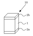
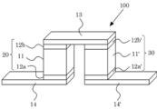
- thermoelectric conversion element It is explanatory drawing for demonstrating the structure of a thermoelectric conversion element. It is explanatory drawing for demonstrating the structure of a thermoelectric conversion module. It is a figure which shows one example of the sintering shrinkage curve of a laminated structure.
- thermoelectric conversion element The thermoelectric conversion element of the present invention has a thermoelectric conversion material layer and an electrode layer.
- thermoelectric conversion material layer is a layer formed of a thermoelectric conversion material represented by the following chemical formula (1).
- M shows the metal material containing at least any one of Mn, Fe, Co, Ni, and Zn
- x shows the numerical value of 0-3.
- thermoelectric conversion material formed of the thermoelectric conversion material represented by the chemical formula (1) has the same crystal structure as tetrahedrite ore obtained from nature, is called tetrahedrite, has low toxicity and It is composed of sulfur (S) and copper (Cu), which have a large amount of crustal reserves, as the main composition, has a high dimensionless figure of merit ZT, and is characterized by being lightweight.
- the dimensionless figure of merit ZT the present inventors have confirmed that the tetrahedrite exhibits a high dimensionless figure of merit ZT in a wide temperature range from room temperature to 400 ° C.
- M in the chemical formula (1) preferably contains at least Ni from the viewpoint of achieving an excellent dimensionless figure of merit ZT.
- M Mn, Fe, Co, and Zn that can provide the same effect among the 3d transition elements of the periodic table that have an electron configuration similar to that of Ni and that have similar chemical and physical properties. Can be used.
- M may include a metal material other than Mn, Fe, Co, Ni and Zn as long as the characteristics of the tetrahedrite are not impaired, but at least any of Mn, Fe, Co, Ni and Zn. It is preferable to select from such metal materials.
- X in the chemical formula (1) is a numerical value of 0 or more and 3 or less that exhibits electric characteristics similar to a crystal structure having a space group of I-43m within a numerical range, and has a higher dimensionless figure of merit ZT. From the viewpoint of achieving the above, a numerical value of 0.5 or more and 1.5 or less is preferable.
- thermoelectric conversion material layer there is no restriction
- the electrode layer is a layer formed of an electrode material that is bonded to the thermoelectric conversion material layer and includes at least one of Fe, Ni, Nb, Pd, Pt, and Au.
- Fe, Ni, Nb, Pd, Pt, and Au have a melting point (700 ° C. or higher) that is sufficiently higher than the melting point of the tetrahedrite. Have been confirmed to be stable.
- these electrode materials are low in electrical resistivity and high in thermal conductivity, and thus are suitable materials for forming the electrode layer.
- the electrode material may contain a small amount of elements other than Fe, Ni, Nb, Pd, Pt and Au as long as it is chemically stable with respect to the tetrahedrite, but Fe, Ni, Nb, It is preferable that at least one of Pd, Pt, and Au is a main component, or at least one of these elements is selected.
- the electrode forming material from the viewpoint of obtaining a lower electric resistance, at least one of Ni, Pd, and Au is a main component, or more preferably selected from at least any of these elements. preferable.
- the electrode material is not particularly limited, and those manufactured by a known manufacturing method or commercially available products can be used.
- the electrode material is in a state of powder, foil, plate, or the like. What was processed can be used.
- thermoelectric conversion element 10 shown in FIG. 1 is an explanatory diagram for explaining a configuration of a thermoelectric conversion element.
- the thermoelectric conversion element 10 shown in FIG. 1 has the same element configuration as a general thermoelectric conversion element.
- the thermoelectric conversion element 10 is configured such that the thermoelectric conversion material layer 1 is sandwiched between two electrode layers 2a and 2b.
- the electrode layers 2a and 2b electrically and thermally connect the thermoelectric conversion material layer 1 and a bonding electrode to be described later to transfer current and heat well, while the thermoelectric conversion material layer 1 and the bonding electrode It has a role of suppressing reaction and a role of relaxing stress between the thermoelectric conversion material layer 1 and the bonding electrode.
- thermoelectric conversion module 100 shown in FIG. 2 has the same module configuration as a general thermoelectric conversion module.
- the thermoelectric conversion module 100 includes two thermoelectric conversion elements, a thermoelectric conversion element 20 and a thermoelectric conversion element 30, one upper electrode 13 arranged so as to bridge between the two thermoelectric conversion elements, and a thermoelectric conversion element. 20 and the lower electrodes 14 and 14 'disposed below the thermoelectric conversion element 30, respectively, and as shown in FIG.
- the upper electrode 13 and the lower electrodes 14 and 14 ' correspond to the above-described bonding electrodes.
- thermoelectric conversion element 20 has a configuration in which the thermoelectric conversion material layer 11 is sandwiched between the two electrode layers 12a and 12b, as in the thermoelectric conversion element 10, and the thermoelectric conversion element 30 also includes two thermoelectric conversion material layers 11 ′.
- the electrode layers 12a ′ and 12b ′ are sandwiched.
- thermoelectric conversion element 20 is a P-type thermoelectric conversion element
- thermoelectric conversion element 30 is an N-type thermoelectric conversion element
- the upper electrode 13 side is set to a high temperature
- the lower electrodes 14, 14 ′ side is set to a low temperature.
- thermoelectric power generation module that generates a potential difference between the lower electrodes 14-14 ′.
- thermoelectric conversion element 20 is a P-type thermoelectric conversion element
- thermoelectric conversion element 30 is an N-type thermoelectric conversion element, and a positive voltage is applied to the lower electrode 14 ′ and a negative voltage is applied to the lower electrode 14.
- thermoelectric conversion material layer When a voltage is applied so that current is introduced into the module from the lower electrode 14 ′ and current is sent from the lower electrode 14, a heat absorption phenomenon occurs on the upper electrode 13 side, and the lower electrodes 14, 14 are applied. It can be used as a Peltier cooling module that generates a heat radiation phenomenon on the side and lowers the temperature of an object in contact with the upper electrode 13.
- thermoelectric conversion materials thermoelectric conversion elements, thermoelectric conversion modules, and the like may be differently used in various situations.
- the material forming the thermoelectric conversion material layer is referred to as a thermoelectric conversion material.
- thermoelectric conversion element having a thermoelectric conversion material layer and an electrode layer is referred to as a thermoelectric conversion element, and having a thermoelectric conversion element and a bonding electrode is referred to as a thermoelectric conversion module, a thermoelectric conversion material, The concept is made higher in order of the thermoelectric conversion element and the thermoelectric conversion module.
- thermoelectric conversion element (Method for manufacturing thermoelectric conversion element)
- the manufacturing method of the thermoelectric conversion element of this invention is a method of manufacturing the said thermoelectric conversion element of this invention, and includes a laminated structure formation process and a heating process.
- the laminated structure forming step is a step of forming a laminated structure in which the thermoelectric conversion material layer and the electrode layer are laminated.
- the laminated structure formation process There is no restriction
- the thermoelectric conversion material may be annealed at an appropriate heating temperature in advance.
- the heating step is a step of heating the laminated structure to sinter the thermoelectric conversion material layer and joining the thermoelectric conversion material layer and the electrode layer.
- the heating step has a role of improving the density of the thermoelectric conversion material layer that is sintered while being joined to the electrode layer.
- the density of the thermoelectric conversion material layer (the tetrahedrite) is improved, a low electrical resistivity can be obtained and a good electrical conductor can be obtained.
- the density at which a low electrical resistivity is obtained is preferably 90% or more, more preferably 95% or more, and particularly preferably 98% or more with respect to the theoretical density of the tetrahedrite.
- the heating temperature in the heating step is preferably 350 ° C. or higher and the melting point of the laminated structure or lower.
- FIG. 3 shows an example of the sintering shrinkage curve of the laminated structure. This sintering shrinkage curve shows the measurement result of how much the length of the laminated structure shrinks depending on the heating temperature when the thermoelectric conversion material layer and the electrode layer are laminated and heated. is there. As shown in FIG. 3, the tetrahedrite constituting the thermoelectric conversion material layer starts to shrink from 350 ° C. with the electrode layer disposed, and begins to change from a powder state to a sintered body to be densified. (Improvement of density) proceeds.
- the lower limit of the heating temperature is not particularly limited, but is preferably 350 ° C. or higher because of the role.
- an upper limit of the said heating temperature it is 700 degrees C or less lower than melting
- a normal pressure sintering method in which firing is performed without applying external pressure is widely known and generally used (see Reference 1 below).
- the temperature rise (heating) is used as a driving force (driving force) to sinter the materials and join different materials. Heating is the most important driving force that promotes sintering and bonding.
- the pressure sintering method is particularly effective for hard-to-sinter bodies such as carbonized tungsten. However, since tetrahedrite is not a hard-to-sinter body, the pressure-sintering method is not indispensable.
- the atmospheric pressure sintering method is applicable as well as the bonded body.
- pressurization becomes a driving force together with heating to promote sintering and bonding. Pressurization is performed when the driving force is not sufficient for heating alone. That is, the tetrahedrite can be bonded to the electrode layer by sintering at a temperature not lower than 350 ° C. and not higher than the melting point without applying external pressure.
- Reference 1 Japan Ceramics Association edited by "Ceramic Engineering Handbook” Basic Volume 2 “Firing and sintering”, pp 202-226 (2014)
- pressurization at the time of sintering has a role of improving the density of the thermoelectric conversion material layer, and is advantageous in forming the thermoelectric conversion material layer. That is, when the density of the thermoelectric conversion material layer (the tetrahedrite) is improved, a low electrical resistivity can be obtained and a good electrical conductor can be obtained. Therefore, the heating is performed in a pressurized environment from the viewpoint of realizing sintering of the thermoelectric conversion material having a small gap and high density and firmly bonding the thermoelectric conversion material layer and the electrode layer. It is preferable to carry out by applying a pressure of 10 MPa or more.
- the pressure in the pressurizing and heating step is larger, an improvement in the density of the tetrahedrite sintered body can be expected, and further, the bonding between the thermoelectric conversion material layer and the electrode layer becomes stronger.
- the upper limit of the applied pressure is not particularly limited, and is, for example, about 500 MPa which is a pressurization limit of a general pressurizing and heating apparatus, and about 200 MPa in consideration of cost.
- a density of 95% or more, further 98% or more can be obtained with respect to the theoretical density of the tetrahedrite.
- thermoelectric generation module has the thermoelectric conversion element of the present invention.
- thermoelectric conversion element can be modularized as shown in the above-described example of the thermoelectric conversion module (see FIG. 2), and the thermoelectric conversion element of the known thermoelectric power generation module is replaced with the thermoelectric conversion element of the present invention.
- thermoelectric power generation module according to the objective can be comprised.
- the Peltier cooling module of this invention has the said thermoelectric conversion element of this invention.
- thermoelectric conversion element can be modularized as shown in the above-described example of the thermoelectric conversion module (see FIG. 2), and the thermoelectric conversion element of the known Peltier cooling module is replaced with the thermoelectric conversion element of the present invention.
- the Peltier cooling module according to the purpose can be configured.
- Example 1-1 ⁇ Production of thermoelectric conversion element> First, Cu (0.6324 g), Ni (0.053 g), Sb (0.4408 g), and S (0.3774 g) as raw materials are vacuum sealed in a quartz tube and melted at 700 ° C. Obtained 1.5 g of a polycrystalline sample of Cu 11 Ni 1 Sb 4 S 13 . The composition analysis of the obtained polycrystalline sample was performed by powder X-ray diffraction. Next, a powdered version of this polycrystalline sample is formed into pellets and annealed at 500 ° C. to remove the second phase Cu 3 SbS 4 as an impurity phase, and tetrahedrite having the above composition Got.
- the obtained tetrahedrite powder in a cylindrical mold made of graphite having an inner diameter of 10 mm has a melting point (700 ° C. or higher) sufficiently higher than the melting point of the tetrahedrite, and has an electrical resistivity.
- a melting point 700 ° C. or higher
- Au powder having a low thermal conductivity and a sintering operation was performed in an inert gas under conditions of heating at 530 ° C., applying 70 MPa pressure, and maintaining for 1 hour.
- the thermoelectric conversion element according to Example 1-1 having a structure in which the thermoelectric conversion material layer formed of tetrahedrite was sandwiched between Au electrode layers was manufactured.
- thermoelectric conversion element obtained as described above has a resistance value of 10 m ⁇ predicted from the electrical resistivity of tetrahedrite alone, whereas the resistance value of the thermoelectric conversion element made using Au powder is 10 m ⁇ . There was no increase in resistance, and good bonding was obtained.
- the density of the tetrahedrite in the thermoelectric conversion element was 4.96 g ⁇ cm ⁇ 3 when measured using a dry automatic densimeter (Micromeritics, Accupic II 1340). This corresponds to 99% of the theoretical density of 5.0 g ⁇ cm ⁇ 3 of the tetrahedrite.
- thermoelectric conversion element according to Example 1-1 is used in a predetermined temperature range (room temperature of about 25 ° C. to about 150 ° C.) using a heat exchange efficiency measuring device (manufactured by Advance Riko Co., Ltd., mini-PEM). The conversion efficiency of was measured. In the measurement, a temperature difference is given to both ends of the thermoelectric conversion element in a vacuum, and the temperature at both ends of the thermoelectric conversion element, the heat flow moving through the thermoelectric conversion element, and the current and voltage flowing through the thermoelectric conversion element are precisely measured. Measured.
- the electromotive force P out generated in the thermoelectric conversion element according to Example 1-1, and the amount of heat Q flowing out from the low temperature side end (low temperature side electrode layer) of the thermoelectric conversion element according to Example 1-1 was determined.
- the heat quantity Q out is measured by measuring the temperature rise of the cooling water for cooling the low temperature side electrode layer with high accuracy, and calculating the amount of heat flowing into the low temperature side electrode layer from the product of the flow rate and heat capacity of the cooling water. The calculation method was used.
- thermoelectric conversion elements prepared using Au powder as the raw material for the electrode layer are shown in Tables 1-1-1 to 1-1-3 below.
- Table 1-1-1 the temperature of one end (high temperature side electrode layer) of the thermoelectric conversion element according to Example 1-1 is 49 ° C. in vacuum, and the other end (low temperature) of the thermoelectric conversion element is shown in Table 1-1-1.
- Table 1-1-2 below shows the measurement results when the measurement was performed under the condition that the temperature of the side electrode layer) was 22 ° C.
- Table 1-1-2 below shows that the temperature of the high temperature side electrode layer is 97 ° C.
- Table 1-1-3 shows the measurement results when the measurement was performed under the condition of °C, and the measurement of the temperature of the high temperature side electrode layer was 147.0 ° C and the temperature of the low temperature side electrode layer was 25 °C The measurement result when performing is shown.
- the temperature in the electrode layers at both ends of the thermoelectric conversion element according to Example 1-1 was measured by a thermocouple in contact with the surface of each electrode layer.
- thermoelectric conversion material layer and the electrode layer can be stably bonded and can be stably manufactured, and a predetermined temperature range (about 25 at room temperature). It can be seen that a thermoelectric conversion element having high thermoelectric conversion characteristics at a temperature of about 150 ° C. to about 150 ° C. can be used stably in a light-weight and high-temperature environment.
- Example 1-2 having a structure in which a thermoelectric conversion material layer formed of tetrahedrite is sandwiched between Au electrode layers in the same manner as Example 1-1 except that an Au foil is used instead of Au powder
- the thermoelectric conversion element which concerns on this was able to be manufactured.
- the thermoelectric conversion element obtained as described above has a resistance value of 10 m ⁇ predicted from the electrical resistivity of the tetrahedrite alone, whereas the resistance value of the thermoelectric conversion element made using Au foil is 10 m ⁇ . There was no increase in resistance, and good bonding was obtained.
- Tables 1-2-1 to 1-2-2 Various measurement results of thermoelectric conversion elements prepared using Au foil as a raw material for the electrode layer are shown in Tables 1-2-1 to 1-2-2 below.
- Table 1-2-1 the temperature of one end (high temperature side electrode layer) of the thermoelectric conversion element according to Example 1-1 is 100 ° C. in vacuum, and the other end (low temperature) of the thermoelectric conversion element is shown in Table 1-2-1.
- Table 1-2-2 shows the measurement results when the temperature of the side electrode layer) is 23 ° C.
- Table 1-2-2 below shows that the temperature of the high temperature side electrode layer is 199 ° C. and the temperature of the low temperature side electrode layer is 23 ° C. The measurement result when measured under the condition of ° C. is shown.
- the temperature in the electrode layers at both ends of the thermoelectric conversion element according to Example 1-2 was measured by a thermocouple in contact with the surface of each electrode layer.
- thermoelectric conversion material layer and the electrode layer can be stably bonded and can be stably manufactured, and a predetermined temperature range (about 25 at room temperature). It can be seen that the thermoelectric conversion element has high thermoelectric conversion characteristics at a temperature of about 200 ° C. to about 200 ° C., is lightweight, and can be used stably in a high temperature environment.
- Example 2-1 having a structure in which a thermoelectric conversion material layer formed of tetrahedrite is sandwiched between Ni electrode layers in the same manner as Example 1-1 except that Ni powder is used instead of Au powder
- the thermoelectric conversion element which concerns on this was able to be manufactured.
- the resistance of the obtained element increased slightly to 7 m ⁇ with respect to the resistance value predicted from the electrical resistivity of tetrahedrite alone, but no significant increase was observed. There is no formation.
- Example 2-2 having a structure in which a thermoelectric conversion material layer formed of tetrahedrite is sandwiched between Ni electrode layers in the same manner as Example 1-1 except that Ni foil is used instead of Au powder
- the thermoelectric conversion element which concerns on this was able to be manufactured.
- the resistance of the obtained element increased slightly to 7 m ⁇ with respect to the resistance value predicted from the electrical resistivity of tetrahedrite alone, but no significant increase was observed. There is no formation.
- Example 3 having a structure in which the thermoelectric conversion material layer formed of tetrahedrite is sandwiched between Fe electrode layers is performed in the same manner as Example 1-1 except that Fe powder is used instead of Au powder.
- a thermoelectric conversion element could be manufactured. The resistance of the obtained element was slightly increased with respect to the resistance value predicted from the electrical resistivity of tetrahedrite alone, but it was less than 10 times, and no significant increase was observed. There is no formation.
- Example 4 having a structure in which a thermoelectric conversion material layer formed of tetrahedrite is sandwiched between Pt electrode layers is the same as Example 1-1 except that Pt powder is used instead of Au powder.
- a thermoelectric conversion element could be manufactured. The resistance of the obtained element was slightly increased with respect to the resistance value predicted from the electrical resistivity of tetrahedrite alone, but it was less than 10 times, and no significant increase was observed. There is no formation.
- Example 5 having a structure in which a thermoelectric conversion material layer formed of tetrahedrite is sandwiched between Nb electrode layers is the same as Example 1-1 except that Nb powder is used instead of Au powder.
- a thermoelectric conversion element could be manufactured. The resistance of the obtained element was slightly increased with respect to the resistance value predicted from the electrical resistivity of tetrahedrite alone, but it was less than 10 times, and no significant increase was observed. There is no formation.
- Example 6-1 Example 6-1 having a structure in which a thermoelectric conversion material layer formed of tetrahedrite is sandwiched between Pd electrode layers in the same manner as Example 1-1 except that Pd powder is used instead of Au powder
- the thermoelectric conversion element which concerns on this was able to be manufactured.
- the resistance of the obtained element was slightly increased with respect to the resistance value predicted from the electrical resistivity of tetrahedrite alone, but it was less than 10 times, and no significant increase was observed. There is no formation.
- Example 6-2 having a structure in which a thermoelectric conversion material layer formed of tetrahedrite is sandwiched between Pd electrode layers in the same manner as Example 1-1 except that Pd foil is used instead of Au powder.
- the thermoelectric conversion element which concerns on this was able to be manufactured.
- the obtained thermoelectric conversion element did not increase as much as 21 m ⁇ with respect to the resistance value estimated from the electrical resistivity of tetrahedrite alone, and a good junction was obtained.
- the conversion efficiency of the thermoelectric conversion element according to Example 6-2 was measured by the same method as in Example 1-1. The measurement results are shown in Tables 2-1 and 2-2 below.
- Table 2-1 below shows that the temperature of one end (high temperature side electrode layer) of the thermoelectric conversion element according to Example 6-2 is 100 ° C. in the vacuum, and the other end (low temperature side electrode) of the thermoelectric conversion element.
- Table 2-2 below shows the measurement results when the measurement was performed under the condition that the temperature of the layer) was 22 ° C.
- Table 2-2 below shows the conditions under which the temperature of the high temperature side electrode layer was 199 ° C. The measurement result when measuring is shown.
- thermoelectric conversion material layer and the electrode layer can be stably bonded, can be stably manufactured, and have a predetermined temperature range (about room temperature). 25.degree. C. to about 200.degree. C.), it can be seen that the thermoelectric conversion element has high thermoelectric conversion characteristics, is lightweight, and can be used stably in a high temperature environment.
- Example 1-1 except that Au powder was not used, only tetrahedrite powder was sintered, and liquid metal In-Ga was applied to both ends of the obtained tetrahedrite sintered body.
- a thermoelectric conversion element according to Comparative Example 1-1 was manufactured.
- thermoelectric conversion element according to Comparative Example 1-2 was performed in the same manner as Comparative Example 1-1 except that liquid metal In—Ga—Bi was used instead of liquid metal In—Ga. Manufactured.
- thermoelectric conversion element In each thermoelectric conversion element according to Comparative Examples 1-1 and 1-2, the In—Ga electrode layer and the In—Ga—Bi electrode layer were bonded to the tetrahedrite sintered body at a use temperature of about 100 ° C. or higher. Reaction occurred in the middle, and a part of the tetrahedrite sintered body was altered, and a high resistance layer was formed at the joint interface between them. From the above, it was concluded that the liquid metals In—Ga and In—Ga—Bi cannot be used for tetrahedrite thermoelectric conversion elements.
- thermoelectric conversion material layer formed of tetrahedrite is sandwiched between Ag electrode layers in the same manner as Example 1-1 except that Ag powder is used instead of Au powder.
- the product formed by the reaction between the tetrahedrite powder and the Ag powder melts, and then the melted material overflows from the sintering mold, and the thermoelectric conversion according to Comparative Example 2 The device could not be manufactured.
- the electrode layer is required to have low electrical resistivity, high thermal conductivity, and chemical stability even at high temperatures.
- electrical resistivity is low, power can be efficiently extracted from tetrahedrite, and when thermal conductivity is high, heat can be efficiently transferred to tetrahedrite, and it is chemically stable even at high temperatures.
- tetrahedrite can be stably used as a thermoelectric conversion material even at high temperatures. Therefore, in Examples 1-1 to 6-2, among metals having low electrical resistivity and high thermal conductivity, Fe, Ni, Nb, Pd, Pt, and Au having a high melting point are selected as electrode materials. ing.
- Ag used in Comparative Example 2 is an electrode material having a high melting point among metals having a low electrical resistivity and a high thermal conductivity (see Table 3 below for the melting point). Therefore, it was considered that Ag can be applied to a tetrahedrite-based thermoelectric conversion element.
- thermoelectric conversion material layer formed of tetrahedrite was sandwiched between Sb electrode layers in the same manner as Example 1-1 except that Sb powder was used instead of Au powder.
- Sb powder was used instead of Au powder.
- the product formed by the reaction of the tetrahedrite powder and the Sb powder melts during the sintering operation, and then the melted material overflows from the sintering mold, The thermoelectric conversion element according to Comparative Example 3 could not be manufactured.
- Ni which is an electrode material used in Example 2-1 and Example 2-2, is a constituent element of tetrahedrite used in the examples, has high affinity with tetrahedrite, and has altered tetrahedrite. It is considered that there is a low possibility of causing it.
- Comparative Example 3 when Sb, which is also a constituent element of tetrahedrite, was used as an electrode material, a reaction occurred and a result that did not function as an electrode layer was obtained. As shown in Table 5 below, the melting point of Sb was higher than the sintering temperature of 530 ° C., but as described above, the Sb powder melted at a low temperature. It is presumed that the unknown characteristics of tetrahedrite have an influence on this result, similar to the description in Comparative Example 2.
- Example 4 As a simple method for forming an electrode layer, there is a method of using a silver (Ag) paste that is generally widely used in electrical equipment. In Example 1-1, except that only tetrahedrite powder was sintered without using Au powder, silver paste was applied to both ends of the obtained tetrahedrite sintered body, and dried. A thermoelectric conversion element according to Comparative Example 4 was produced in the same manner as in 1-1.
- thermoelectric conversion element according to Comparative Example 4 When the resistance of the thermoelectric conversion element according to Comparative Example 4 was measured, a resistance value (200 m ⁇ ) that was 10 times larger than the resistance value (20 m ⁇ ) predicted from the electrical resistivity of tetrahedrite alone was confirmed. It was confirmed that a low-resistance electrode layer could not be obtained when the electrode material was used. As a cause of this result, it is considered that Ag reacted with tetrahedrite, as in Comparative Example 2 (Ag powder). Tetra, which is a new thermoelectric conversion material, is widely used in widely used electrode materials. It can be seen that the unknown characteristics of hedrite cannot be applied to a tetrahedrite-based thermoelectric conversion element.
Landscapes
- Engineering & Computer Science (AREA)
- Chemical & Material Sciences (AREA)
- Mechanical Engineering (AREA)
- Manufacturing & Machinery (AREA)
- Materials Engineering (AREA)
- Metallurgy (AREA)
- Composite Materials (AREA)
- Organic Chemistry (AREA)
- Inorganic Chemistry (AREA)
- General Engineering & Computer Science (AREA)
- Thermal Sciences (AREA)
- Physics & Mathematics (AREA)
- Powder Metallurgy (AREA)
Abstract
【課題】テトラヘドライトで形成される熱電変換材料層と電極層とが安定して接合可能で、高温環境下での使用時に熱電変換材料の変質が抑えられ、安定して製造可能な熱電変換素子及びその製造方法を提供すること、更に、前記熱電変換素子を用いた熱電発電モジュール及びペルチェ冷却モジュールを提供すること。 【解決手段】本発明の熱電変換素子は、下記化学式(1)で表される熱電変換材料で形成される熱電変換材料層と、前記熱電変換材料層と接合されFe、Ni、Nb、Pd、Pt及びAuの少なくともいずれかを含む電極材料で形成される電極層と、を有することを特徴とする。 Cu12-xMxSb4S13 (1) ただし、前記化学式(1)中、Mは、Mn、Fe、Co、Ni及びZnの少なくともいずれかを含む金属材料を示し、xは、0以上3以下の数値を示す。ことを特徴とする。
Description
本発明は、テトラへドライトを熱電変換材料に用いる熱電変換素子とその製造方法、及び前記熱電変換素子を有する熱電発電モジュールとペルチェ冷却モジュールに関する。
熱電変換とは、固体の熱電変換素子を用いて熱エネルギーと電気エネルギーを相互に変換する技術である。
熱エネルギーを電気エネルギーに変換する技術は、熱電発電と呼ばれ、熱電効果の1つであるゼーベック効果に基づく。
一方、電気エネルギーから熱エネルギーへの変換は、ペルチェ効果に由来し、冷却や精密温調に応用されている。ここでは、ペルチェ効果に由来する電気エネルギーから熱エネルギーへの変換をペルチェ冷却と称する。
前記熱電発電による発電装置や前記ペルチェ冷却による温調装置は、機械的な可動部を有さず、静音、無振動、長寿命、小型化しても変換効率が変わらない、という長所を併せ持つ。
熱エネルギーを電気エネルギーに変換する技術は、熱電発電と呼ばれ、熱電効果の1つであるゼーベック効果に基づく。
一方、電気エネルギーから熱エネルギーへの変換は、ペルチェ効果に由来し、冷却や精密温調に応用されている。ここでは、ペルチェ効果に由来する電気エネルギーから熱エネルギーへの変換をペルチェ冷却と称する。
前記熱電発電による発電装置や前記ペルチェ冷却による温調装置は、機械的な可動部を有さず、静音、無振動、長寿命、小型化しても変換効率が変わらない、という長所を併せ持つ。
前記熱電発電では、前記熱電変換素子の両端間の温度差が電気エネルギーに直接変換される。この発電方法は、化石燃料を用いる発電と比較して環境に優しい発電技術である。また、この熱電発電を利用して、工場や自動車から排出されている膨大な未利用熱エネルギーを回収し、そこから電力を生み出すこととすれば、化石燃料の消費量低減、更にはCO2削減と省エネルギー化に大いに貢献できる。
また、前記ペルチェ冷却では、前記熱電変換素子に直流電流を通電した際に前記熱電変換素子の片端が冷却される現象を用いている。このペルチェ冷却は、フロンガスなどの冷媒を必要としない点、及び電流制御に基づく冷却温度を精密に制御できる点を長所としている。
前記熱電発電及び前記ペルチェ冷却の双方に用いられる前記熱電変換素子は、熱電変換材料で形成される熱電変換材料層と電極材料で形成される電極層から形成される。ここで、前記電極材料には、前記熱電変換材料層と、前記電極層の前記熱電変換材料層と接合する面と反対側の面に配される接合電極とを電気的、熱的に接続して、電流や熱を良く伝える一方で、前記熱電変換材料と前記接合電極との反応を抑制する役割や、前記熱電変換材料層と前記接合電極との間の応力を緩和する役割が求められる。
前記熱電変換材料の性能は、無次元性能指数ZTとして表すことができ、このZTが高いほど性能が優れている。無次元性能指数ZTは、次式、ZT=S2T/ρκで表され、Sは、前記熱電変換材料のゼーベック係数を示し、Tは、絶対温度を示し、ρは、前記熱電変換材料の電気抵抗率を示し、κは、熱電変換材料の熱伝導率を示す。
ここで、高い無次元性能指数を示す高性能熱電変換材料として、化学組成がCu12-xMxSb4S13(ただし、Mは、Mn、Fe、Co、Ni、及びZnの少なくともいずれかを含む金属材料を示し、xは、0以上3以下の数値を示す)で表される、「テトラヘドライト」と呼ばれる熱電変換材料が提案されている。このテトラヘドライトは、400℃で高い無次元性能指数ZT(0.5~1.0)を示すことが報告されている(例えば、特許文献1、非特許文献1、非特許文献2参照)。
また、高温(400℃)の環境で使用できる熱電変換材料として、鉛テルライド(PbTe)が知られている(非特許文献3参照)。
しかしながら、前記鉛テルライドは、毒性を持つ鉛(Pb)と地殻埋蔵量が少ないテルル(Te)から構成される。対して、Cu12-xMxSb4S13で表されるテトラヘドライト系の熱電変換材料は、低毒性であり、かつ地殻埋蔵量が多い銅(Cu)と硫黄(S)から主に構成されるとともに、高い無次元性能指数ZTを有し、軽量(鉛テルライドの密度:8.2gcm-3、テトラヘドライトの密度:5.0gcm-3)であるという特徴を有している。
したがって、前記熱電変換材料としては、前記テトラヘドライトが適している。
また、高温(400℃)の環境で使用できる熱電変換材料として、鉛テルライド(PbTe)が知られている(非特許文献3参照)。
しかしながら、前記鉛テルライドは、毒性を持つ鉛(Pb)と地殻埋蔵量が少ないテルル(Te)から構成される。対して、Cu12-xMxSb4S13で表されるテトラヘドライト系の熱電変換材料は、低毒性であり、かつ地殻埋蔵量が多い銅(Cu)と硫黄(S)から主に構成されるとともに、高い無次元性能指数ZTを有し、軽量(鉛テルライドの密度:8.2gcm-3、テトラヘドライトの密度:5.0gcm-3)であるという特徴を有している。
したがって、前記熱電変換材料としては、前記テトラヘドライトが適している。
前記熱電変換材料層と前記電極層から構成される前記熱電変換素子の性能は、前記熱電変換素子に与えた熱量Qinが、どの程度電力Poutとして取り出されるかを示す変換効率η(=Pout/Qin)で評価される(非特許文献4参照)。
ηを高くするためには、前記熱電変換材料のZTを高くすることと、優れた性能を有する電極層を形成することが必要である。
即ち、前記電極層には、先述の通り、電気抵抗率が低く、熱伝導率が高く、高温でも化学的に安定であること等が求められる。このような電極層を形成することで、前記熱電発電においては、効率良く熱を前記熱電変換材料に与えられ、得られる起電力を損失が少なく取り出せる。また、前記ペルチェ冷却においては、少ない損失で直流電流を前記熱電変換材料に通電でき、接触させる対象から熱を効率良く奪うことができる。
ηを高くするためには、前記熱電変換材料のZTを高くすることと、優れた性能を有する電極層を形成することが必要である。
即ち、前記電極層には、先述の通り、電気抵抗率が低く、熱伝導率が高く、高温でも化学的に安定であること等が求められる。このような電極層を形成することで、前記熱電発電においては、効率良く熱を前記熱電変換材料に与えられ、得られる起電力を損失が少なく取り出せる。また、前記ペルチェ冷却においては、少ない損失で直流電流を前記熱電変換材料に通電でき、接触させる対象から熱を効率良く奪うことができる。
しかしながら、異なる材料で形成される前記熱電変換材料層と前記電極層とを高温の環境下で使用に耐えるように安定に接合させ、これを保持することは容易ではない。高温の環境下でも前記熱電変換材料と反応することのない前記電極材料で前記電極層を形成する必要がある。
殊に、前記テトラヘドライトは、低毒性かつ地殻埋蔵量が多い元素から構成されるとともに、高い無次元性能指数ZTを示し、軽量化に対応可能である一方で、他の物質と反応性の高い硫黄(S)を主成分とするため、使用時に前記電極層材料と反応して前記熱電変換材料が変質したり、前記電極層と前記熱電変換材料層の界面に高抵抗層が生じたり、製造時に不良が生じる問題がある。
殊に、前記テトラヘドライトは、低毒性かつ地殻埋蔵量が多い元素から構成されるとともに、高い無次元性能指数ZTを示し、軽量化に対応可能である一方で、他の物質と反応性の高い硫黄(S)を主成分とするため、使用時に前記電極層材料と反応して前記熱電変換材料が変質したり、前記電極層と前記熱電変換材料層の界面に高抵抗層が生じたり、製造時に不良が生じる問題がある。
K. Suekuni, K. Tsuruta, T. Ariga, and M. Koyano, 「Thermoelectric Properties of Mineral Tetrahedrites Cu10Tr2Sb4S13 with Low Thermal Conductivity」Applied Physics Express, 5号, 051201-1~3ページ,2012年5月.
Koichiro Suekuni, Kojiro Tsuruta, Masaru Kunii, Hirotaka Nishiate, Eiji Nishibori, Sachiko Maki, Michihiro Ohta, Atsushi Yamamoto, and Mikio Koyano, 「High-performance thermoelectric mineral Cu12-xNixSb4S13 tetrahedrite」, Journal of Applied Physics, 113号, 043712-1~5ページ, 2013年1月
G. Jeffrey Snyder, Eric S. Toberer, 「Complex thermoelectric materials」, Nature Materials, 7号, 105~114ページ,2008年
Hsin Wang, Robin McCarty, James R. Salvador, Atsushi Yamamoto, Jan Koenig, 「Determination of Thermoelectric Module Efficiency: A Survey」, Journal of Electronic Materials, 43号, 2274~2286ページ,2014年6月
本発明は、従来技術における前記諸問題を解決し、前記テトラヘドライトで形成される前記熱電変換材料層と前記電極層とが安定して接合可能で、高温環境下での使用時に前記熱電変換材料の変質が抑えられ、安定して製造可能な熱電変換素子及びその製造方法を提供すること、更に、前記熱電変換素子を用いた熱電発電モジュール及びペルチェ冷却モジュールを提供することを目的とする。
前記課題を解決するため、本発明者は、前記テトラヘドライトで形成される前記熱電変換材料層と前記電極層とが安定して接合可能で、高温環境下での使用時に前記熱電変換材料の変質が抑えられ、前記熱電変換材料層を有する前記熱電変換素子として安定して製造可能な前記電極材料について鋭意検討を行った。
その結果、前記テトラヘドライトには、未だ知られていない特性が多く残されており、好適な電極材料の選定が難航したが、試行錯誤の結果、幾つかの電極材料で前記電極層を形成すると、前記課題を解決できることの知見を得た。
その結果、前記テトラヘドライトには、未だ知られていない特性が多く残されており、好適な電極材料の選定が難航したが、試行錯誤の結果、幾つかの電極材料で前記電極層を形成すると、前記課題を解決できることの知見を得た。
本発明は、前記知見に基づくものであり、前記課題を解決するための手段としては、以下の通りである。即ち、
<1> 下記化学式(1)で表される熱電変換材料で形成される熱電変換材料層と、前記熱電変換材料層と接合されFe、Ni、Nb、Pd、Pt及びAuの少なくともいずれかを含む電極材料で形成される電極層と、を有することを特徴とする熱電変換素子。

ただし、前記化学式(1)中、Mは、Mn、Fe、Co、Ni及びZnの少なくともいずれかを含む金属材料を示し、xは、0以上3以下の数値を示す。
<2> 電極材料がNi、Pd及びAuの少なくともいずれかを含む前記<1>に記載の熱電変換素子。
<3> 化学式(1)中のMが、少なくともNiを含む金属材料を示す前記<1>から<2>のいずれかに記載の熱電変換素子。
<4> 化学式(1)中のxが、0.5以上1.5以下の数値を示す前記<1>から<3>のいずれかに記載の熱電変換素子。
<5> 前記<1>から<4>のいずれかに記載の熱電変換素子の製造方法であって、熱電変換材料層と電極層とが積層された積層構造体を形成する積層構造体形成工程と、前記積層構造体を加熱して前記熱電変換材料層を焼結させるとともに前記熱電変換材料層と電極層とを接合させる加熱工程と、を含むことを特徴とする熱電変換素子の製造方法。
<6> 加熱工程における加熱温度が350℃以上積層構造体の融点以下の温度である前記<5>に記載の熱電変換素子の製造方法。
<7> 加熱工程における加熱を加圧下で実施する前記<5>から<6>のいずれかに記載の熱電変換素子の製造方法。
<8> 加圧する圧力が小さくとも10MPaである前記<7>に記載の熱電変換素子の製造方法。
<9> 前記<1>から<4>のいずれかに記載の熱電変換素子を有して構成されることを特徴とする熱電発電モジュール。
<10> 前記<1>から<4>のいずれかに記載の熱電変換素子を有して構成されることを特徴とするペルチェ冷却モジュール。
<1> 下記化学式(1)で表される熱電変換材料で形成される熱電変換材料層と、前記熱電変換材料層と接合されFe、Ni、Nb、Pd、Pt及びAuの少なくともいずれかを含む電極材料で形成される電極層と、を有することを特徴とする熱電変換素子。
<2> 電極材料がNi、Pd及びAuの少なくともいずれかを含む前記<1>に記載の熱電変換素子。
<3> 化学式(1)中のMが、少なくともNiを含む金属材料を示す前記<1>から<2>のいずれかに記載の熱電変換素子。
<4> 化学式(1)中のxが、0.5以上1.5以下の数値を示す前記<1>から<3>のいずれかに記載の熱電変換素子。
<5> 前記<1>から<4>のいずれかに記載の熱電変換素子の製造方法であって、熱電変換材料層と電極層とが積層された積層構造体を形成する積層構造体形成工程と、前記積層構造体を加熱して前記熱電変換材料層を焼結させるとともに前記熱電変換材料層と電極層とを接合させる加熱工程と、を含むことを特徴とする熱電変換素子の製造方法。
<6> 加熱工程における加熱温度が350℃以上積層構造体の融点以下の温度である前記<5>に記載の熱電変換素子の製造方法。
<7> 加熱工程における加熱を加圧下で実施する前記<5>から<6>のいずれかに記載の熱電変換素子の製造方法。
<8> 加圧する圧力が小さくとも10MPaである前記<7>に記載の熱電変換素子の製造方法。
<9> 前記<1>から<4>のいずれかに記載の熱電変換素子を有して構成されることを特徴とする熱電発電モジュール。
<10> 前記<1>から<4>のいずれかに記載の熱電変換素子を有して構成されることを特徴とするペルチェ冷却モジュール。
本発明によれば、従来技術における前記諸問題を解決することができ、前記テトラヘドライトで形成される前記熱電変換材料層と前記電極層とが安定して接合可能で、高温環境下での使用時に前記熱電変換材料の変質が抑えられ、安定して製造可能な熱電変換素子及びその製造方法を提供すること、更に、前記熱電変換素子を用いた熱電発電モジュール及びペルチェ冷却モジュールを提供することができる。
(熱電変換素子)
本発明の熱電変換素子は、熱電変換材料層と、電極層とを有する。
本発明の熱電変換素子は、熱電変換材料層と、電極層とを有する。
<熱電変換材料層>
前記熱電変換材料層は、下記化学式(1)で表される熱電変換材料で形成される層である。
前記熱電変換材料層は、下記化学式(1)で表される熱電変換材料で形成される層である。

前記化学式(1)で表される熱電変換材料で形成される前記熱電変換材料は、天然から得られるテトラヘドライト鉱と同じ結晶構造を有しており、テトラヘドライトと呼ばれ、低毒性かつ地殻埋蔵量が多い硫黄(S)と銅(Cu)を主な組成として構成されるとともに、高い無次元性能指数ZTを有し、更に、軽量であるとの特徴を有する。無次元性能指数ZTに関し、本発明者らは、前記テトラヘドライトが室温~400℃の広い温度範囲において高い無次元性能指数ZTを示すことを確認している。
前記化学式(1)中のMとしては、優れた無次元性能指数ZTを達成する観点から、少なくともNiを含むことが好ましい。
また、Mとしては、Niと類似の電子配置を有し、化学的・物理的な性質が似ている周期律表の3d遷移元素の中でも同様の効果を提供可能なMn、Fe、Co及びZnを使用できる。
また、Mとしては、前記テトラヘドライトの特徴を損なわない限り、Mn、Fe、Co、Ni及びZn以外の金属材料を含むこととしてもよいが、Mn、Fe、Co、Ni及びZnの少なくともいずれかの金属材料から選択されることが好ましい。
また、Mとしては、Niと類似の電子配置を有し、化学的・物理的な性質が似ている周期律表の3d遷移元素の中でも同様の効果を提供可能なMn、Fe、Co及びZnを使用できる。
また、Mとしては、前記テトラヘドライトの特徴を損なわない限り、Mn、Fe、Co、Ni及びZn以外の金属材料を含むこととしてもよいが、Mn、Fe、Co、Ni及びZnの少なくともいずれかの金属材料から選択されることが好ましい。
前記化学式(1)中のxとしては、数値範囲内でI-43mの空間群を持つ結晶構造と類似の電気的な特性を奏する0以上3以下の数値であり、より高い無次元性能指数ZTを達成する観点から、0.5以上1.5以下の数値であることが好ましい。
前記熱電変換材料層の形成材料としての前記テトラヘドライトとしては、特に制限はなく、公知の製造方法、例えば、特許文献1、非特許文献1,2等に記載の製造方法により製造することができる。
<電極層>
前記電極層は、前記熱電変換材料層と接合されFe、Ni、Nb、Pd、Pt及びAuの少なくともいずれかを含む電極材料で形成される層である。
前記電極層は、前記熱電変換材料層と接合されFe、Ni、Nb、Pd、Pt及びAuの少なくともいずれかを含む電極材料で形成される層である。
Fe、Ni、Nb、Pd、Pt及びAuは、前記テトラヘドライトの融点より十分に高い融点(700℃以上)を有し、後述する実施例での実施結果から前記テトラヘドライトに対して化学的に安定であることが確認されている。また、これらの電極材料は、電気抵抗率が低く、熱伝導率が高いため、前記電極層を形成する材料として好適な材料である。
前記電極材料としては、前記テトラヘドライトに対して化学的に安定であれば、Fe、Ni、Nb、Pd、Pt及びAu以外の元素を少量含むこととしてもよいが、Fe、Ni、Nb、Pd、Pt及びAuの少なくともいずれかの元素を主成分とするか、又は、これら元素の少なくともいずれから選択されることが好ましい。中でも、前記電極形成材料としては、より低い電気抵抗を得る観点から、Ni、Pd及びAuの少なくともいずれかの元素を主成分とするか、又は、これら元素の少なくともいずれから選択されることがより好ましい。
前記電極材料としては、前記テトラヘドライトに対して化学的に安定であれば、Fe、Ni、Nb、Pd、Pt及びAu以外の元素を少量含むこととしてもよいが、Fe、Ni、Nb、Pd、Pt及びAuの少なくともいずれかの元素を主成分とするか、又は、これら元素の少なくともいずれから選択されることが好ましい。中でも、前記電極形成材料としては、より低い電気抵抗を得る観点から、Ni、Pd及びAuの少なくともいずれかの元素を主成分とするか、又は、これら元素の少なくともいずれから選択されることがより好ましい。
また、前記電極材料としては、特に制限はなく、公知の製造方法で製造されたものや市販品を用いることができ、前記電極層の形成に際し、粉末状、箔状、板状等の状態に加工されたものを用いることができる。
前記熱電変換素子の一実施形態を図1に示す。図1は、熱電変換素子の構成を説明するための説明図である。なお、図1に示す熱電変換素子10は、一般的な熱電変換素子の素子構成と同様のものである。
熱電変換素子10は、熱電変換材料層1が2つの電極層2a,2bで挟持された構成とされる。
電極層2a,2bは、熱電変換材料層1と、後述する接合電極とを電気的、熱的に接続して、電流や熱を良く伝える一方で、熱電変換材料層1と前記接合電極との反応を抑制する役割、及び熱電変換材料層1と前記接合電極と間の応力を緩和する役割を有する。
熱電変換素子10は、熱電変換材料層1が2つの電極層2a,2bで挟持された構成とされる。
電極層2a,2bは、熱電変換材料層1と、後述する接合電極とを電気的、熱的に接続して、電流や熱を良く伝える一方で、熱電変換材料層1と前記接合電極との反応を抑制する役割、及び熱電変換材料層1と前記接合電極と間の応力を緩和する役割を有する。
次に、前記熱電変換素子を用いて構成した熱電変換モジュールの一実施形態を図2に示す。図2は、熱電変換モジュールの構成を説明するための説明図である。なお、図2に示す熱電変換モジュール100は、一般的な熱電変換モジュールのモジュール構成と同様のものである。
熱電変換モジュール100は、熱電変換素子20と熱電変換素子30の2つの熱電変換素子と、上部にこれら2つの熱電変換素子間を架け渡すように配される1つの上部電極13と、熱電変換素子20及び熱電変換素子30の下部にそれぞれ配される下部電極14,14’とで構成され、図2に示すように全体がπ型の形状とされる。上部電極13及び下部電極14,14’は、前述の接合電極に相当する。
また、熱電変換素子20は、熱電変換素子10と同様、熱電変換材料層11が2つの電極層12a,12bで挟持された構成とされ、熱電変換素子30も熱電変換材料層11’が2つの電極層12a’,12b’で挟持された構成とされる。
熱電変換モジュール100は、熱電変換素子20と熱電変換素子30の2つの熱電変換素子と、上部にこれら2つの熱電変換素子間を架け渡すように配される1つの上部電極13と、熱電変換素子20及び熱電変換素子30の下部にそれぞれ配される下部電極14,14’とで構成され、図2に示すように全体がπ型の形状とされる。上部電極13及び下部電極14,14’は、前述の接合電極に相当する。
また、熱電変換素子20は、熱電変換素子10と同様、熱電変換材料層11が2つの電極層12a,12bで挟持された構成とされ、熱電変換素子30も熱電変換材料層11’が2つの電極層12a’,12b’で挟持された構成とされる。
熱電変換モジュール100においては、熱電変換素子20がP型熱電変換素子であるとともに熱電変換素子30がN型熱電変換素子であり、上部電極13側を高温にし、下部電極14,14’側を低温にすると、下部電極14-14’間に電位差を生じさせる熱電発電モジュールとして利用することができる。
また、熱電変換モジュール100においては、熱電変換素子20がP型熱電変換素子であるとともに熱電変換素子30がN型熱電変換素子であり、下部電極14’にプラス、下部電極14にマイナスの電圧を印加して、下部電極14’からモジュール中に電流を導入し、下部電極14から電流を送出させるように電圧を印加すると、上部電極13側では熱の吸収現象が発生し、下部電極14、14’側で放熱現象が発生して、上部電極13に接する対象の温度を低下させるペルチェ冷却モジュールとして利用することができる 。
なお、熱電変換材料、熱電変換素子、熱電変換モジュールなどの呼称は、種々の場面で異なる呼称が採用されることがあるが、本明細書では、熱電変換材料層を形成する材料を熱電変換材料と呼称し、熱電変換材料層と電極層とを有するものを熱電変換素子と呼称し、熱電変換素子と接合電極とを有して構成されるものを熱電変換モジュールと呼称し、熱電変換材料、熱電変換素子、熱電変換モジュールの順でより高次化された概念とする。
また、熱電変換モジュール100においては、熱電変換素子20がP型熱電変換素子であるとともに熱電変換素子30がN型熱電変換素子であり、下部電極14’にプラス、下部電極14にマイナスの電圧を印加して、下部電極14’からモジュール中に電流を導入し、下部電極14から電流を送出させるように電圧を印加すると、上部電極13側では熱の吸収現象が発生し、下部電極14、14’側で放熱現象が発生して、上部電極13に接する対象の温度を低下させるペルチェ冷却モジュールとして利用することができる 。
なお、熱電変換材料、熱電変換素子、熱電変換モジュールなどの呼称は、種々の場面で異なる呼称が採用されることがあるが、本明細書では、熱電変換材料層を形成する材料を熱電変換材料と呼称し、熱電変換材料層と電極層とを有するものを熱電変換素子と呼称し、熱電変換素子と接合電極とを有して構成されるものを熱電変換モジュールと呼称し、熱電変換材料、熱電変換素子、熱電変換モジュールの順でより高次化された概念とする。
(熱電変換素子の製造方法)
本発明の熱電変換素子の製造方法は、本発明の前記熱電変換素子を製造する方法であり、積層構造体形成工程と、加熱工程とを含む。
本発明の熱電変換素子の製造方法は、本発明の前記熱電変換素子を製造する方法であり、積層構造体形成工程と、加熱工程とを含む。
<積層構造体形成工程>
前記積層構造体形成工程は、前記熱電変換材料層と前記電極層とが積層された積層構造体を形成する工程である。
前記積層構造体形成工程の実施方法としては、特に制限はなく、例えば、ペレット状に固めた前記熱電変換材料の上下両側に粉末状、箔状、板状等の前記電極材料を配する方法が挙げられる。
なお、前記積層構造体形成工程の実施に際し、事前に前記熱電変換材料を適当な加熱温度でアニール処理を行ってもよい。
前記積層構造体形成工程は、前記熱電変換材料層と前記電極層とが積層された積層構造体を形成する工程である。
前記積層構造体形成工程の実施方法としては、特に制限はなく、例えば、ペレット状に固めた前記熱電変換材料の上下両側に粉末状、箔状、板状等の前記電極材料を配する方法が挙げられる。
なお、前記積層構造体形成工程の実施に際し、事前に前記熱電変換材料を適当な加熱温度でアニール処理を行ってもよい。
前記加熱工程は、前記積層構造体を加熱して前記熱電変換材料層を焼結させるとともに前記熱電変換材料層と前記電極層とを接合させる工程である。
前記加熱工程は、前記電極層と接合された状態で焼結される前記熱電変換材料層の密度を向上させる役割を有する。前記熱電変換材料層(前記テトラヘドライト)の密度を向上させると、低い電気抵抗率が得られ、電気の良伝導体とすることができる。なお、低い電気抵抗率が得られる密度としては、前記テトラヘドライトの理論密度に対して90%以上が好ましく、95%以上がより好ましく、98%以上が特に好ましい。
前記役割のため、前記加熱工程における加熱温度としては、350℃以上、前記積層構造体の融点以下の温度であることが好ましい。
図3に前記積層構造体の焼結収縮曲線の1例を示す。この焼結収縮曲線は、前記熱電変換材料層と前記電極層とを積層させた状態で加熱し、前記積層構造体の長さが加熱温度によってどの程度収縮するかの測定結果を示したものである。
該図3に示すように、前記熱電変換材料層を構成する前記テトラヘドライトは、前記電極層を配した状態で350℃から収縮が始まり、粉末等の状態から焼結体に変わり始め緻密化(密度の向上)が進む。
したがって、前記加熱温度の下限としては、特に制限はないが、前記役割のため、350℃以上が好ましい。なお、前記加熱温度の上限としては、前記電極材料及び前記テトラヘドライトの融点よりも低い700℃以下である。
図3に前記積層構造体の焼結収縮曲線の1例を示す。この焼結収縮曲線は、前記熱電変換材料層と前記電極層とを積層させた状態で加熱し、前記積層構造体の長さが加熱温度によってどの程度収縮するかの測定結果を示したものである。
該図3に示すように、前記熱電変換材料層を構成する前記テトラヘドライトは、前記電極層を配した状態で350℃から収縮が始まり、粉末等の状態から焼結体に変わり始め緻密化(密度の向上)が進む。
したがって、前記加熱温度の下限としては、特に制限はないが、前記役割のため、350℃以上が好ましい。なお、前記加熱温度の上限としては、前記電極材料及び前記テトラヘドライトの融点よりも低い700℃以下である。
焼結体の製造方法として、外部からの圧力をかけずに焼成する常圧焼結法が広く知られており、一般に良く使用されている(下記参考文献1参照)。
この方法では、温度上昇(加熱)を駆動力(ドライビング・フォース)として、材料を焼結させるとともに異種材料を接合させる工程である。加熱が焼結と接合を促進させるもっとも重要な駆動力である。
加圧焼結法は、炭素化タングステンなどの難焼結体に対しては特に効果を有するが、テトラヘドライトは難焼結体ではないため、加圧焼結法は必須ではなく、前記焼結体と同様に常圧焼結法も適用可能である。前記加圧焼結法では、加熱とともに加圧が駆動力となり、焼結と接合を促進させる。駆動力が加熱だけでは足りない時に、加圧を行う。
即ち、前記テトラヘドライトは、外部からの圧力をかけないで、350℃以上、融点以下の温度を駆動力として焼結と前記電極層を接合させることが可能である。
参考文献1;(社)日本セラミクス協会編,「セラミック工学ハンドブック」基礎第2編6.「焼成と焼結」、pp202-226(2014)
この方法では、温度上昇(加熱)を駆動力(ドライビング・フォース)として、材料を焼結させるとともに異種材料を接合させる工程である。加熱が焼結と接合を促進させるもっとも重要な駆動力である。
加圧焼結法は、炭素化タングステンなどの難焼結体に対しては特に効果を有するが、テトラヘドライトは難焼結体ではないため、加圧焼結法は必須ではなく、前記焼結体と同様に常圧焼結法も適用可能である。前記加圧焼結法では、加熱とともに加圧が駆動力となり、焼結と接合を促進させる。駆動力が加熱だけでは足りない時に、加圧を行う。
即ち、前記テトラヘドライトは、外部からの圧力をかけないで、350℃以上、融点以下の温度を駆動力として焼結と前記電極層を接合させることが可能である。
参考文献1;(社)日本セラミクス協会編,「セラミック工学ハンドブック」基礎第2編6.「焼成と焼結」、pp202-226(2014)
ただし、焼結時の加圧は、前記熱電変換材料層の密度を向上させる役割を有し、前記熱電変換材料層を形成するうえで有利となる。即ち、前記熱電変換材料層(前記テトラヘドライト)の密度を向上させると、低い電気抵抗率が得られ、電気の良伝導体とすることができる。
したがって、空隙が少なく高密度な前記熱電変換材料の焼結を実現するとともに、前記熱電変換材料層と前記電極層とを強固に接合させる観点から、前記加熱としては、加圧環境下で実施することが好ましく、10MPa以上の圧力をかけて実施することがより好ましい。なお、前記加圧加熱工程における圧力としては大きい程、前記テトラヘドライト焼結体の密度の向上が期待でき、更に、前記熱電変換材料層と前記電極層との接合が強固となることから、印加圧力の上限としては、特に制限はなく、例えば、一般的な加圧加熱装置の加圧限界である500MPa程度、コストなどを考慮すると200MPa程度である。
前記加熱温度及び前記圧力の数値範囲で、前記テトラヘドライトを焼結させると、前記テトラヘドライトの理論密度に対して95%以上、更には98%以上の密度を得ることができる。
したがって、空隙が少なく高密度な前記熱電変換材料の焼結を実現するとともに、前記熱電変換材料層と前記電極層とを強固に接合させる観点から、前記加熱としては、加圧環境下で実施することが好ましく、10MPa以上の圧力をかけて実施することがより好ましい。なお、前記加圧加熱工程における圧力としては大きい程、前記テトラヘドライト焼結体の密度の向上が期待でき、更に、前記熱電変換材料層と前記電極層との接合が強固となることから、印加圧力の上限としては、特に制限はなく、例えば、一般的な加圧加熱装置の加圧限界である500MPa程度、コストなどを考慮すると200MPa程度である。
前記加熱温度及び前記圧力の数値範囲で、前記テトラヘドライトを焼結させると、前記テトラヘドライトの理論密度に対して95%以上、更には98%以上の密度を得ることができる。
なお、前記加熱工程の実施方法としては、特に制限はなく、例えば、公知の加熱装置や加圧加熱装置中に前記積層構造体を配して、これを加熱や加圧加熱する方法が挙げられる。
(熱電発電モジュール)
本発明の熱電発電モジュールは、本発明の前記熱電変換素子を有する。
前記熱電発電モジュールの前記熱電変換素子以外のモジュール構成としては、特に制限はなく、目的に応じて適宜選択することができ、公知の熱電発電モジュールの構成から適宜選択することができる。
即ち、前記熱電変換素子は、前述の熱電変換モジュールの例(図2参照)に示すようにモジュール化することができ、公知の熱電発電モジュールの熱電変換素子を本発明の前記熱電変換素子に置き換えることで、目的に応じた前記熱電発電モジュールを構成することができる。
本発明の熱電発電モジュールは、本発明の前記熱電変換素子を有する。
前記熱電発電モジュールの前記熱電変換素子以外のモジュール構成としては、特に制限はなく、目的に応じて適宜選択することができ、公知の熱電発電モジュールの構成から適宜選択することができる。
即ち、前記熱電変換素子は、前述の熱電変換モジュールの例(図2参照)に示すようにモジュール化することができ、公知の熱電発電モジュールの熱電変換素子を本発明の前記熱電変換素子に置き換えることで、目的に応じた前記熱電発電モジュールを構成することができる。
(ペルチェ冷却モジュール)
本発明のペルチェ冷却モジュールは、本発明の前記熱電変換素子を有する。
前記ペルチェ冷却モジュールの前記熱電変換素子以外のモジュール構成としては、特に制限はなく、目的に応じて適宜選択することができ、公知のペルチェ冷却モジュールの構成から適宜選択することができる。
即ち、前記熱電変換素子は、前述の熱電変換モジュールの例(図2参照)に示すようにモジュール化することができ、公知のペルチェ冷却モジュールの熱電変換素子を本発明の前記熱電変換素子に置き換えることで、目的に応じた前記ペルチェ冷却モジュールを構成することができる。
本発明のペルチェ冷却モジュールは、本発明の前記熱電変換素子を有する。
前記ペルチェ冷却モジュールの前記熱電変換素子以外のモジュール構成としては、特に制限はなく、目的に応じて適宜選択することができ、公知のペルチェ冷却モジュールの構成から適宜選択することができる。
即ち、前記熱電変換素子は、前述の熱電変換モジュールの例(図2参照)に示すようにモジュール化することができ、公知のペルチェ冷却モジュールの熱電変換素子を本発明の前記熱電変換素子に置き換えることで、目的に応じた前記ペルチェ冷却モジュールを構成することができる。
(実施例1-1)
<熱電変換素子の作製>
先ず、原料であるCu(0.6324g)、Ni(0.053g)、Sb(0.4408g)、S(0.3774g)を石英管の中に真空封入し、700℃で溶融させて、組成がCu11Ni1Sb4S13の多結晶試料を1.5g得た。なお、得られた前記多結晶試料の組成分析は、粉末X線回折により行った。
次いで、この多結晶試料を粉末化したものをペレット状に成形し、500℃でアニール処理を行うことにより、不純物相である第二相のCu3SbS4を除去し、前記組成のテトラへドライトを得た。
次いで、グラファイト製の内径10mmの円柱状の型の中にて、得られたテトラヘドライトの粉末を、前記テトラへドライトの融点より十分に高い融点(700℃以上)を有し、電気抵抗率が低く、熱伝導率が高いAu粉末で両側から挟むように積層して、不活性ガス中、530℃加熱、70MPa圧力印加、1時間保持の条件下で焼結操作を行った。
以上により、前記テトラヘドライトで形成される熱電変換材料層がAu電極層で挟持された構造の実施例1-1に係る熱電変換素子を製造できた。
以上のようにして得られた熱電変換素子は、テトラヘドライト単体の電気抵抗率から予測される抵抗値の10mΩに対して、Au粉末を用いて作った熱電変換素子の抵抗値は、10mΩと抵抗の増加がなく、良好な接合が得られた。
なお、この熱電変換素子中の前記テトラヘドライトの密度を、乾式自動密度計(マイクロメリティクス社、アキュピックII 1340)を用いて測定したところ、4.96g・cm-3であった。これは、前記テトラヘドライトの理論密度5.0g・cm-3の99%に当たる。
<熱電変換素子の作製>
先ず、原料であるCu(0.6324g)、Ni(0.053g)、Sb(0.4408g)、S(0.3774g)を石英管の中に真空封入し、700℃で溶融させて、組成がCu11Ni1Sb4S13の多結晶試料を1.5g得た。なお、得られた前記多結晶試料の組成分析は、粉末X線回折により行った。
次いで、この多結晶試料を粉末化したものをペレット状に成形し、500℃でアニール処理を行うことにより、不純物相である第二相のCu3SbS4を除去し、前記組成のテトラへドライトを得た。
次いで、グラファイト製の内径10mmの円柱状の型の中にて、得られたテトラヘドライトの粉末を、前記テトラへドライトの融点より十分に高い融点(700℃以上)を有し、電気抵抗率が低く、熱伝導率が高いAu粉末で両側から挟むように積層して、不活性ガス中、530℃加熱、70MPa圧力印加、1時間保持の条件下で焼結操作を行った。
以上により、前記テトラヘドライトで形成される熱電変換材料層がAu電極層で挟持された構造の実施例1-1に係る熱電変換素子を製造できた。
以上のようにして得られた熱電変換素子は、テトラヘドライト単体の電気抵抗率から予測される抵抗値の10mΩに対して、Au粉末を用いて作った熱電変換素子の抵抗値は、10mΩと抵抗の増加がなく、良好な接合が得られた。
なお、この熱電変換素子中の前記テトラヘドライトの密度を、乾式自動密度計(マイクロメリティクス社、アキュピックII 1340)を用いて測定したところ、4.96g・cm-3であった。これは、前記テトラヘドライトの理論密度5.0g・cm-3の99%に当たる。
<熱電変換特性の評価>
次に、熱交換効率の測定装置(アドバンス理工社製、mini-PEM)を用い、所定の温度範囲(室温である約25℃~約150℃)において、実施例1-1に係る熱電変換素子の変換効率を測定した。測定では、真空中で熱電変換素子の両端に温度差を与えて、前記熱電変換素子の両端の温度、前記熱電変換素子中を移動する熱流量、及び前記熱電変換素子に流れる電流、電圧を精密に測定した。
前記測定装置において、実施例1-1に係る熱電変換素子に発生する起電力Pout、実施例1-1に係る熱電変換素子の低温側の端部(低温側電極層)から流出する熱量Qoutを精密に測定して、ヒーターから実施例1-1に係る熱電変換素子の一端(高温側電極層)に流入する熱量Qin(=Pout+Qout)を求めた。変換効率ηは、η=Pout/Qinから求めた。
なお、熱量Qoutの測定には、前記低温側電極層を冷却する冷却水の温度上昇分を高精度に測定し、冷却水の流量と熱容量の積から前記低温側電極層に流入する熱量を算出する方法を用いた。
電極層の原料としてAu粉末を用いて作成した熱電変換素子の測定結果を、下記表1-1-1~1-1-3に示す。なお、下記表1-1-1は、真空中で、実施例1-1に係る熱電変換素子の一端(高温側電極層)の温度が49℃、熱電変換素子のもう一方の端部(低温側電極層)の温度が22℃の条件で測定を行った場合の測定結果を示し、下記表1-1-2は、高温側電極層の温度が97℃、低温側電極層の温度が24℃の条件で測定を行った場合の測定結果を示し、下記表1-1-3は、高温側電極層の温度が147.0℃、低温側電極層の温度が25℃の測定条件で測定を行った場合の測定結果を示す。
測定結果を得る際、実施例1-1に係る熱電変換素子の両端の電極層における温度をそれぞれの電極層の表面に接触させた熱電対によって測定した。
次に、熱交換効率の測定装置(アドバンス理工社製、mini-PEM)を用い、所定の温度範囲(室温である約25℃~約150℃)において、実施例1-1に係る熱電変換素子の変換効率を測定した。測定では、真空中で熱電変換素子の両端に温度差を与えて、前記熱電変換素子の両端の温度、前記熱電変換素子中を移動する熱流量、及び前記熱電変換素子に流れる電流、電圧を精密に測定した。
前記測定装置において、実施例1-1に係る熱電変換素子に発生する起電力Pout、実施例1-1に係る熱電変換素子の低温側の端部(低温側電極層)から流出する熱量Qoutを精密に測定して、ヒーターから実施例1-1に係る熱電変換素子の一端(高温側電極層)に流入する熱量Qin(=Pout+Qout)を求めた。変換効率ηは、η=Pout/Qinから求めた。
なお、熱量Qoutの測定には、前記低温側電極層を冷却する冷却水の温度上昇分を高精度に測定し、冷却水の流量と熱容量の積から前記低温側電極層に流入する熱量を算出する方法を用いた。
電極層の原料としてAu粉末を用いて作成した熱電変換素子の測定結果を、下記表1-1-1~1-1-3に示す。なお、下記表1-1-1は、真空中で、実施例1-1に係る熱電変換素子の一端(高温側電極層)の温度が49℃、熱電変換素子のもう一方の端部(低温側電極層)の温度が22℃の条件で測定を行った場合の測定結果を示し、下記表1-1-2は、高温側電極層の温度が97℃、低温側電極層の温度が24℃の条件で測定を行った場合の測定結果を示し、下記表1-1-3は、高温側電極層の温度が147.0℃、低温側電極層の温度が25℃の測定条件で測定を行った場合の測定結果を示す。
測定結果を得る際、実施例1-1に係る熱電変換素子の両端の電極層における温度をそれぞれの電極層の表面に接触させた熱電対によって測定した。
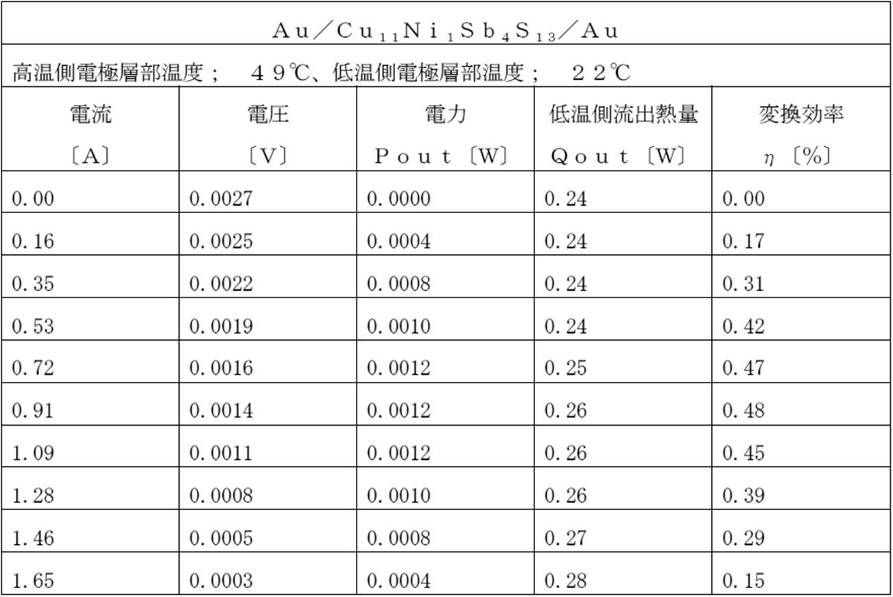

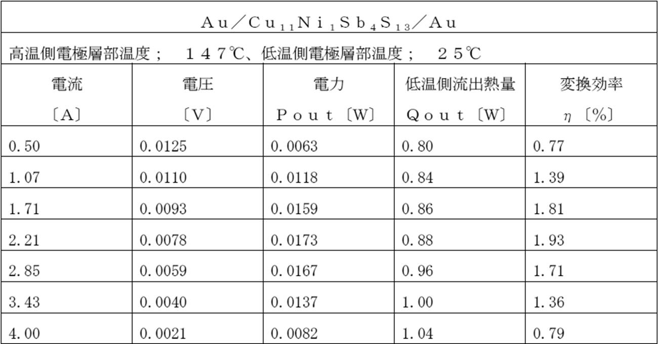
以上の通り、実施例1-1に係る熱電変換素子は、熱電変換材料層と電極層とが安定して接合可能で安定して製造可能であるとともに、所定の温度範囲(室温である約25℃~約150℃)において、高い熱電変換特性を有し、軽量、かつ高温の環境で安定して使用可能な熱電変換素子となり得ることが分かる。
(実施例1-2)
Au粉末に代えてAu箔を用いたこと以外は実施例1-1と同様にして、前記テトラヘドライトで形成される熱電変換材料層がAu電極層で挟持された構造の実施例1-2に係る熱電変換素子を製造することができた。
以上のようにして得られた熱電変換素子は、テトラヘドライト単体の電気抵抗率から予測される抵抗値の10mΩに対して、Au箔を用いて作った熱電変換素子の抵抗値は、10mΩと抵抗の増加がなく、良好な接合が得られた。
電極層の原料としてAu箔を用いて作成した熱電変換素子の各種測定結果を、下記表1-2-1~1-2-2に示す。なお、下記表1-2-1は、真空中で、実施例1-1に係る熱電変換素子の一端(高温側電極層)の温度が100℃、熱電変換素子のもう一方の端部(低温側電極層)の温度が23℃の条件で測定を行った場合の測定結果を示し、下記表1-2-2は、高温側電極層の温度が199℃、低温側電極層の温度が23℃の条件で測定を行った場合の測定結果を示す。
測定結果を得る際、実施例1-2に係る熱電変換素子の両端の電極層における温度をそれぞれの電極層の表面に接触させた熱電対によって測定した。
Au粉末に代えてAu箔を用いたこと以外は実施例1-1と同様にして、前記テトラヘドライトで形成される熱電変換材料層がAu電極層で挟持された構造の実施例1-2に係る熱電変換素子を製造することができた。
以上のようにして得られた熱電変換素子は、テトラヘドライト単体の電気抵抗率から予測される抵抗値の10mΩに対して、Au箔を用いて作った熱電変換素子の抵抗値は、10mΩと抵抗の増加がなく、良好な接合が得られた。
電極層の原料としてAu箔を用いて作成した熱電変換素子の各種測定結果を、下記表1-2-1~1-2-2に示す。なお、下記表1-2-1は、真空中で、実施例1-1に係る熱電変換素子の一端(高温側電極層)の温度が100℃、熱電変換素子のもう一方の端部(低温側電極層)の温度が23℃の条件で測定を行った場合の測定結果を示し、下記表1-2-2は、高温側電極層の温度が199℃、低温側電極層の温度が23℃の条件で測定を行った場合の測定結果を示す。
測定結果を得る際、実施例1-2に係る熱電変換素子の両端の電極層における温度をそれぞれの電極層の表面に接触させた熱電対によって測定した。
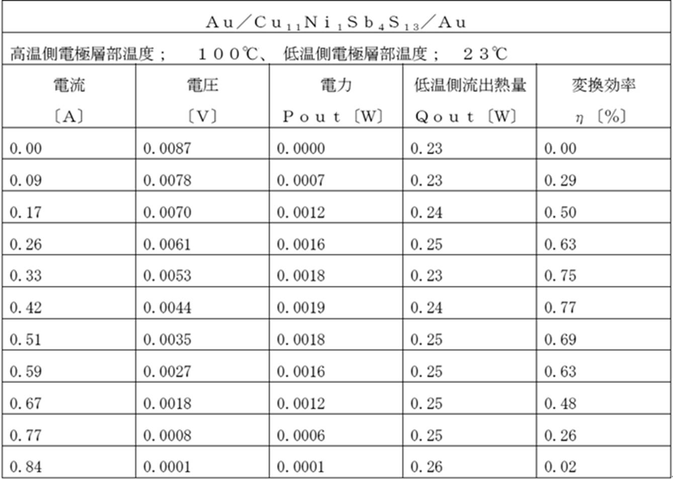
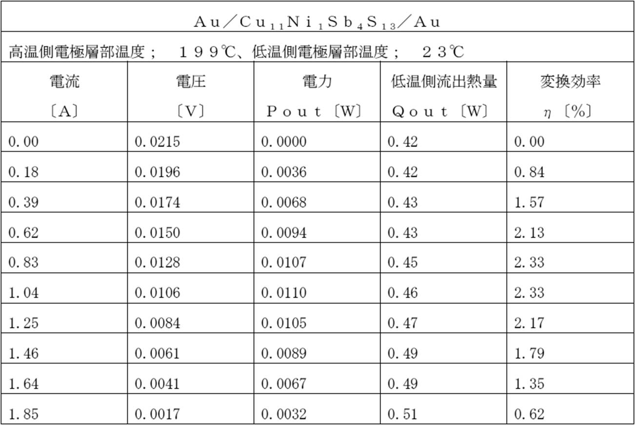
以上の通り、実施例1-2に係る熱電変換素子は、熱電変換材料層と電極層とが安定して接合可能で安定して製造可能であるとともに、所定の温度範囲(室温である約25℃~約200℃)において、高い熱電変換特性を有し、軽量、かつ高温の環境で安定して使用可能な熱電変換素子となり得ることが分かる。
(実施例2-1)
Au粉末に代えてNi粉末を用いたこと以外は実施例1-1と同様にして、前記テトラヘドライトで形成される熱電変換材料層がNi電極層で挟持された構造の実施例2-1に係る熱電変換素子を製造することができた。
なお、得られた素子の抵抗は、テトラヘドライト単体の電気抵抗率から予測される抵抗値の約1mΩに対して、7mΩとやや増加したが、顕著な増加は見られず、高抵抗層の形成はない。
Au粉末に代えてNi粉末を用いたこと以外は実施例1-1と同様にして、前記テトラヘドライトで形成される熱電変換材料層がNi電極層で挟持された構造の実施例2-1に係る熱電変換素子を製造することができた。
なお、得られた素子の抵抗は、テトラヘドライト単体の電気抵抗率から予測される抵抗値の約1mΩに対して、7mΩとやや増加したが、顕著な増加は見られず、高抵抗層の形成はない。
(実施例2-2)
Au粉末に代えてNi箔を用いたこと以外は実施例1-1と同様にして、前記テトラヘドライトで形成される熱電変換材料層がNi電極層で挟持された構造の実施例2-2に係る熱電変換素子を製造することができた。
なお、得られた素子の抵抗は、テトラヘドライト単体の電気抵抗率から予測される抵抗値の約1mΩに対して、7mΩとやや増加したが、顕著な増加は見られず、高抵抗層の形成はない。
Au粉末に代えてNi箔を用いたこと以外は実施例1-1と同様にして、前記テトラヘドライトで形成される熱電変換材料層がNi電極層で挟持された構造の実施例2-2に係る熱電変換素子を製造することができた。
なお、得られた素子の抵抗は、テトラヘドライト単体の電気抵抗率から予測される抵抗値の約1mΩに対して、7mΩとやや増加したが、顕著な増加は見られず、高抵抗層の形成はない。
(実施例3)
Au粉末に代えてFe粉末を用いたこと以外は実施例1-1と同様にして、前記テトラヘドライトで形成される熱電変換材料層がFe電極層で挟持された構造の実施例3に係る熱電変換素子を製造することができた。
なお、得られた素子の抵抗は、テトラヘドライト単体の電気抵抗率から予測される抵抗値に対して、やや増加したが、10倍未満であり、顕著な増加は見られず、高抵抗層の形成はない。
Au粉末に代えてFe粉末を用いたこと以外は実施例1-1と同様にして、前記テトラヘドライトで形成される熱電変換材料層がFe電極層で挟持された構造の実施例3に係る熱電変換素子を製造することができた。
なお、得られた素子の抵抗は、テトラヘドライト単体の電気抵抗率から予測される抵抗値に対して、やや増加したが、10倍未満であり、顕著な増加は見られず、高抵抗層の形成はない。
(実施例4)
Au粉末に代えてPt粉末を用いたこと以外は実施例1-1と同様にして、前記テトラヘドライトで形成される熱電変換材料層がPt電極層で挟持された構造の実施例4に係る熱電変換素子を製造することができた。
なお、得られた素子の抵抗は、テトラヘドライト単体の電気抵抗率から予測される抵抗値に対して、やや増加したが、10倍未満であり、顕著な増加は見られず、高抵抗層の形成はない。
Au粉末に代えてPt粉末を用いたこと以外は実施例1-1と同様にして、前記テトラヘドライトで形成される熱電変換材料層がPt電極層で挟持された構造の実施例4に係る熱電変換素子を製造することができた。
なお、得られた素子の抵抗は、テトラヘドライト単体の電気抵抗率から予測される抵抗値に対して、やや増加したが、10倍未満であり、顕著な増加は見られず、高抵抗層の形成はない。
(実施例5)
Au粉末に代えてNb粉末を用いたこと以外は実施例1-1と同様にして、前記テトラヘドライトで形成される熱電変換材料層がNb電極層で挟持された構造の実施例5に係る熱電変換素子を製造することができた。
なお、得られた素子の抵抗は、テトラヘドライト単体の電気抵抗率から予測される抵抗値に対して、やや増加したが、10倍未満であり、顕著な増加は見られず、高抵抗層の形成はない。
Au粉末に代えてNb粉末を用いたこと以外は実施例1-1と同様にして、前記テトラヘドライトで形成される熱電変換材料層がNb電極層で挟持された構造の実施例5に係る熱電変換素子を製造することができた。
なお、得られた素子の抵抗は、テトラヘドライト単体の電気抵抗率から予測される抵抗値に対して、やや増加したが、10倍未満であり、顕著な増加は見られず、高抵抗層の形成はない。
(実施例6-1)
Au粉末に代えてPd粉末を用いたこと以外は実施例1-1と同様にして、前記テトラヘドライトで形成される熱電変換材料層がPd電極層で挟持された構造の実施例6-1に係る熱電変換素子を製造することができた。
なお、得られた素子の抵抗は、テトラヘドライト単体の電気抵抗率から予測される抵抗値に対して、やや増加したが、10倍未満であり、顕著な増加は見られず、高抵抗層の形成はない。
Au粉末に代えてPd粉末を用いたこと以外は実施例1-1と同様にして、前記テトラヘドライトで形成される熱電変換材料層がPd電極層で挟持された構造の実施例6-1に係る熱電変換素子を製造することができた。
なお、得られた素子の抵抗は、テトラヘドライト単体の電気抵抗率から予測される抵抗値に対して、やや増加したが、10倍未満であり、顕著な増加は見られず、高抵抗層の形成はない。
(実施例6-2)
Au粉末に代えてPd箔を用いたこと以外は実施例1-1と同様にして、前記テトラヘドライトで形成される熱電変換材料層がPd電極層で挟持された構造の実施例6-2に係る熱電変換素子を製造することができた。
得られた熱電変換素子は、テトラヘドライト単体の電気抵抗率から予測される抵抗値の約10mΩに対して、21mΩと大きな抵抗の増加がなく、良好な接合が得られた。
実施例6-2に係る熱電変換素子の変換効率を、実施例1-1の場合と同じ方法で測定した。
各測定結果を下記表2-1,2-2に示す。なお、下記表2-1は、真空中で、実施例6-2に係る熱電変換素子の一端(高温側電極層)の温度が100℃、熱電変換素子のもう一方の端部(低温側電極層)の温度が22℃の条件で測定を行った場合の測定結果を示し、下記表2-2は、高温側電極層の温度が199℃、低温側電極層の温度が23℃の条件で測定を行った場合の測定結果を示す。
Au粉末に代えてPd箔を用いたこと以外は実施例1-1と同様にして、前記テトラヘドライトで形成される熱電変換材料層がPd電極層で挟持された構造の実施例6-2に係る熱電変換素子を製造することができた。
得られた熱電変換素子は、テトラヘドライト単体の電気抵抗率から予測される抵抗値の約10mΩに対して、21mΩと大きな抵抗の増加がなく、良好な接合が得られた。
実施例6-2に係る熱電変換素子の変換効率を、実施例1-1の場合と同じ方法で測定した。
各測定結果を下記表2-1,2-2に示す。なお、下記表2-1は、真空中で、実施例6-2に係る熱電変換素子の一端(高温側電極層)の温度が100℃、熱電変換素子のもう一方の端部(低温側電極層)の温度が22℃の条件で測定を行った場合の測定結果を示し、下記表2-2は、高温側電極層の温度が199℃、低温側電極層の温度が23℃の条件で測定を行った場合の測定結果を示す。


以上の通り、実施例6-2に係る熱電変換素子は、熱電変換材料層と電極層とが安定して接合可能で、安定して製造可能であるとともに、所定の温度範囲(室温である約25℃~約200℃)において、高い熱電変換特性を有し、軽量、かつ高温の環境で安定して使用可能な熱電変換素子となり得ることが分かる。
(比較例1-1,1-2)
電極層として液体金属In-Gaを使う技術が提案され、Zn4Sb3系、CoSb3系、Bi2Te3系熱電変換材料層と接合させて良好な結果が得られている(下記参考文献2,3参照)。
参考文献2;高澤 弘幸、山本 淳、李 哲虎、太田 敏隆,「液体金属接合によるモジュール性能の向上」、熱電変換シンポジウム2001論文集、pp44-45(2001)
参考文献3;山本 淳、高澤 弘幸、李 哲虎、太田 敏隆,「変換効率10%を目指したセグメント型熱電素子の開発」、2001年度傾斜機能材料論文集、pp44-45(2001),pp1-6(2001)
電極層として液体金属In-Gaを使う技術が提案され、Zn4Sb3系、CoSb3系、Bi2Te3系熱電変換材料層と接合させて良好な結果が得られている(下記参考文献2,3参照)。
参考文献2;高澤 弘幸、山本 淳、李 哲虎、太田 敏隆,「液体金属接合によるモジュール性能の向上」、熱電変換シンポジウム2001論文集、pp44-45(2001)
参考文献3;山本 淳、高澤 弘幸、李 哲虎、太田 敏隆,「変換効率10%を目指したセグメント型熱電素子の開発」、2001年度傾斜機能材料論文集、pp44-45(2001),pp1-6(2001)
実施例1-1において、Au粉末を用いることなく、テトラヘドライト粉末のみを焼結させ、得られたテトラヘドライト焼結体の両端に液体金属In-Gaを塗布したこと以外は、実施例1-1と同様にして、比較例1-1に係る熱電変換素子を製造した。
また、比較例1-1において、液体金属In-Gaに代えて液体金属In-Ga-Biを用いたこと以外は比較例1-1と同様にして、比較例1-2に係る熱電変換素子を製造した。
比較例1-1,1-2に係る各熱電変換素子においては、In-Ga電極層、In-Ga-Bi電極層が、約100℃以上の使用温度で前記テトラヘドライト焼結体との間に反応が生じ、前記テトラヘドライト焼結体の一部が変質し、両者の接合界面に高抵抗層が形成された。
以上から、液体金属In-Ga,In-Ga-Biは、テトラヘドライト系熱電変換素子に使用できないという結論に至った。
以上から、液体金属In-Ga,In-Ga-Biは、テトラヘドライト系熱電変換素子に使用できないという結論に至った。
(比較例2)
Au粉末に代えてAg粉末を用いたこと以外は実施例1-1と同様にして、前記テトラヘドライトで形成される熱電変換材料層がAg電極層で挟持された構造の比較例2に係る熱電変換素子の製造を試みた。
しかしながら、焼結操作中にテトラへドライト粉末とAg粉末とが反応してできた生成物が溶け、その後、溶けた物質が焼結用の型から溢れ出てしまい、比較例2に係る熱電変換素子を製造することができなかった。
Au粉末に代えてAg粉末を用いたこと以外は実施例1-1と同様にして、前記テトラヘドライトで形成される熱電変換材料層がAg電極層で挟持された構造の比較例2に係る熱電変換素子の製造を試みた。
しかしながら、焼結操作中にテトラへドライト粉末とAg粉末とが反応してできた生成物が溶け、その後、溶けた物質が焼結用の型から溢れ出てしまい、比較例2に係る熱電変換素子を製造することができなかった。
電極層には、電気抵抗率が低く、熱伝導率が高く、高温でも化学的に安定であることが求められる。電気抵抗率が低いと、テトラヘドライトから効率良く電力を取り出すことができ、熱伝導率が高いと、テトラヘドライトに効率良く熱を伝えることができ、高温でも化学的に安定していることで、高温でも安定的にテトラヘドライトを熱電変換材料として使用できる。
そこで、実施例1-1~6-2では、電気抵抗率が低く、熱伝導率が高い金属の中で、融点の高い、Fe、Ni、Nb、Pd、Pt、Auを電極材料として選択している。比較例2で用いたAgは、これらと同様に、電気抵抗率が低く、熱伝導率が高い金属の中で、融点の高い電極材料である(融点につき下記表3参照)。したがって、Agは、テトラヘドライト系熱電変換素子に適用することができると考えられた。
そこで、実施例1-1~6-2では、電気抵抗率が低く、熱伝導率が高い金属の中で、融点の高い、Fe、Ni、Nb、Pd、Pt、Auを電極材料として選択している。比較例2で用いたAgは、これらと同様に、電気抵抗率が低く、熱伝導率が高い金属の中で、融点の高い電極材料である(融点につき下記表3参照)。したがって、Agは、テトラヘドライト系熱電変換素子に適用することができると考えられた。

ところが、比較例2における説明の通り、Fe、Ni、Nb、Pd、Pt、Auは、電極層として機能したが、Agは溶けて電極層として機能しなかった。
Agが電極層として機能しなかった理由としては、Agがテトラヘドライトの構成元素の中で最も反応性が高い硫黄(S)と反応したのではないかと推測できる。
しかし、一般的に知られている、各種金属(Fe、Ni、Nb、Pd、Ag、Pt、Au)の硫化物における標準生成自由エネルギー変化を見てみると、各種金属の硫化物の標準生成自由エネルギー変化が負である(下記表4参照、Nb、Auについては、データがないが、硫化物の標準生成自由エネルギー変化が負であると想定される)。
標準生成自由エネルギー変化が負の場合は、硫化物を生成する方向で反応が進み、正の場合では、反応が逆に進み、硫化物が生成されない。なお、下記表4中の数値は、反応の度合いを示す。
したがって、Fe、Ni、Nb、Pd、Ag、Pt、Auは、むしろ、テトラヘドライト中の硫黄(S)と反応することが考えられたが、Fe、Ni、Nb、Pd、Pt、Auを電極材料としてを用いると、実施例1-1~6-2における説明の通り、電極層として機能させることができることが確認された。一方、表中の金属のうち、Agのみ電極層として機能させることができない結果となった。
Agが電極層として機能しなかった理由としては、Agがテトラヘドライトの構成元素の中で最も反応性が高い硫黄(S)と反応したのではないかと推測できる。
しかし、一般的に知られている、各種金属(Fe、Ni、Nb、Pd、Ag、Pt、Au)の硫化物における標準生成自由エネルギー変化を見てみると、各種金属の硫化物の標準生成自由エネルギー変化が負である(下記表4参照、Nb、Auについては、データがないが、硫化物の標準生成自由エネルギー変化が負であると想定される)。
標準生成自由エネルギー変化が負の場合は、硫化物を生成する方向で反応が進み、正の場合では、反応が逆に進み、硫化物が生成されない。なお、下記表4中の数値は、反応の度合いを示す。
したがって、Fe、Ni、Nb、Pd、Ag、Pt、Auは、むしろ、テトラヘドライト中の硫黄(S)と反応することが考えられたが、Fe、Ni、Nb、Pd、Pt、Auを電極材料としてを用いると、実施例1-1~6-2における説明の通り、電極層として機能させることができることが確認された。一方、表中の金属のうち、Agのみ電極層として機能させることができない結果となった。
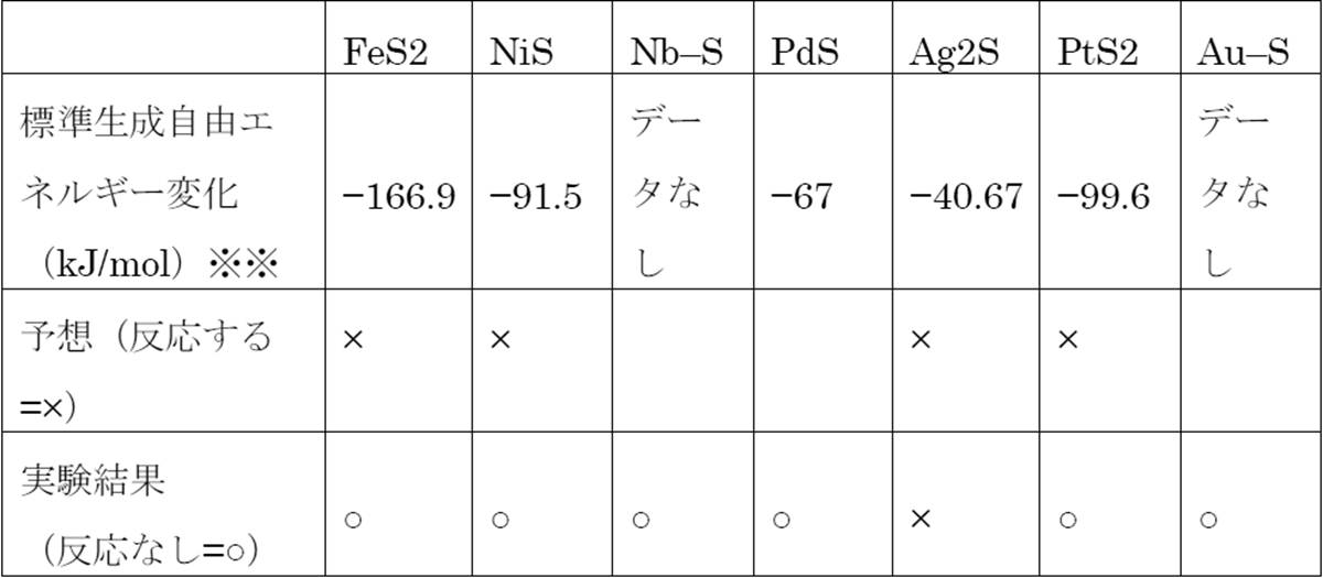
以上のFe、Ni、Nb、Pd、Pt、Auは電極層として機能し、Agは熱電変換物質との反応物を生成し、これが溶けて電極層として機能しないという実験結果は、一般に知られているデータ(融点、標準生成自由エネルギー変化など)からは類推できない事項を示している。2013年に発見された新しいテトラへドライト(特許文献1、非特許文献1,2)には、未だ知られていない熱力学的特性などが存在しており、その未知の特性が実験結果に影響を及ぼしているものと推察される。
(比較例3)
Au粉末に代えてSb粉末を用いたこと以外は実施例1-1と同様にして、前記テトラヘドライトで形成される熱電変換材料層がSb電極層で挟持された構造の比較例3に係る熱電変換素子の製造を試みた。
しかしながら、比較例2と同様に、焼結操作中にテトラへドライト粉末とSb粉末とが反応してできた生成物が溶け、その後、溶けた物質が焼結用の型から溢れ出てしまい、比較例3に係る熱電変換素子を製造することができなかった。
Au粉末に代えてSb粉末を用いたこと以外は実施例1-1と同様にして、前記テトラヘドライトで形成される熱電変換材料層がSb電極層で挟持された構造の比較例3に係る熱電変換素子の製造を試みた。
しかしながら、比較例2と同様に、焼結操作中にテトラへドライト粉末とSb粉末とが反応してできた生成物が溶け、その後、溶けた物質が焼結用の型から溢れ出てしまい、比較例3に係る熱電変換素子を製造することができなかった。
実施例2-1及び実施例2-2で用いた電極材料であるNiは、実施例で用いたテトラへドライトの構成元素であり、テトラへドライトと親和性が高く、テトラヘドライトの変質を生じさせる可能性が低いと考えられる。
しかしながら、比較例3において、同じくテトラへドライトの構成元素であるSbを電極材料として用いると、反応が生じて電極層として機能しない結果が得られた。
下記表5に示すように、Sbの融点は、焼結温度530℃よりは高いが、先の説明の通り、Sb粉末が低温で溶け出す結果となった。
この結果には、比較例2における説明と同様、テトラヘドライトの未知の特性が影響を及ぼしているものと推察される。
しかしながら、比較例3において、同じくテトラへドライトの構成元素であるSbを電極材料として用いると、反応が生じて電極層として機能しない結果が得られた。
下記表5に示すように、Sbの融点は、焼結温度530℃よりは高いが、先の説明の通り、Sb粉末が低温で溶け出す結果となった。
この結果には、比較例2における説明と同様、テトラヘドライトの未知の特性が影響を及ぼしているものと推察される。

(比較例4)
簡便な電極層の形成方法として、一般に広く電気機器で利用されている銀(Ag)ペーストを利用する方法がある。
実施例1-1において、Au粉末を用いることなく、テトラヘドライト粉末のみを焼結させ、得られたテトラヘドライト焼結体の両端に銀ペーストを塗布、乾燥させたこと以外は、実施例1-1と同様にして、比較例4に係る熱電変換素子を製造した。
簡便な電極層の形成方法として、一般に広く電気機器で利用されている銀(Ag)ペーストを利用する方法がある。
実施例1-1において、Au粉末を用いることなく、テトラヘドライト粉末のみを焼結させ、得られたテトラヘドライト焼結体の両端に銀ペーストを塗布、乾燥させたこと以外は、実施例1-1と同様にして、比較例4に係る熱電変換素子を製造した。
比較例4に係る熱電変換素子の抵抗を測定したところ、テトラヘドライト単体の電気抵抗率から予測される抵抗値(20mΩ)よりも10倍も大きな抵抗値(200mΩ)が確認され、銀ペーストを電極材料とすると低抵抗の電極層が得られないことが確認された。
この結果の原因としては、比較例2(Ag粉末)と同様に、Agがテトラヘドライトと反応したことが考えられ、一般に広く利用されている電極材料においても、新たな熱電変換材料であるテトラヘドライトの未知の特性により、テトラヘドライト系熱電変換素子に適用することができないことが分かる。
この結果の原因としては、比較例2(Ag粉末)と同様に、Agがテトラヘドライトと反応したことが考えられ、一般に広く利用されている電極材料においても、新たな熱電変換材料であるテトラヘドライトの未知の特性により、テトラヘドライト系熱電変換素子に適用することができないことが分かる。
1,11,11’ 熱電変換材料層
2a,2b,12a,12b,12a’,12b’ 電極層
10,20,30 熱電変換素子
13 上部接合電極
14,14’ 下部接合電極
100 熱電変換モジュール
2a,2b,12a,12b,12a’,12b’ 電極層
10,20,30 熱電変換素子
13 上部接合電極
14,14’ 下部接合電極
100 熱電変換モジュール
Claims (10)
- 下記化学式(1)で表される熱電変換材料で形成される熱電変換材料層と、
前記熱電変換材料層と接合されFe、Ni、Nb、Pd、Pt及びAuの少なくともいずれかを含む電極材料で形成される電極層と、
を有することを特徴とする熱電変換素子。

- 電極材料がNi、Pd及びAuの少なくともいずれかを含む請求項1に記載の熱電変換素子。
- 化学式(1)中のMが、少なくともNiを含む金属材料を示す請求項1から2のいずれかに記載の熱電変換素子。
- 化学式(1)中のxが、0.5以上1.5以下の数値を示す請求項1から3のいずれかに記載の熱電変換素子。
- 請求項1から4のいずれかに記載の熱電変換素子の製造方法であって、
熱電変換材料層と電極層とが積層された積層構造体を形成する積層構造体形成工程と、
前記積層構造体を加熱して前記熱電変換材料層を焼結させるとともに前記熱電変換材料層と電極層とを接合させる加熱工程と、
を含むことを特徴とする熱電変換素子の製造方法。 - 加熱工程における加熱温度が350℃以上積層構造体の融点以下の温度である請求項5に記載の熱電変換素子の製造方法。
- 加熱工程における加熱を加圧下で実施する請求項5から6のいずれかに記載の熱電変換素子の製造方法。
- 加圧する圧力が小さくとも10MPaである請求項7に記載の熱電変換素子の製造方法。
- 請求項1から4のいずれかに記載の熱電変換素子を有して構成されることを特徴とする熱電発電モジュール。
- 請求項1から4のいずれかに記載の熱電変換素子を有して構成されることを特徴とするペルチェ冷却モジュール。
Applications Claiming Priority (2)
| Application Number | Priority Date | Filing Date | Title |
|---|---|---|---|
| JP2015126846A JP6518887B2 (ja) | 2015-06-24 | 2015-06-24 | 熱電変換素子とその製造方法、及び熱電発電モジュールとペルチェ冷却モジュール |
| JP2015-126846 | 2015-06-24 |
Publications (1)
| Publication Number | Publication Date |
|---|---|
| WO2016208561A1 true WO2016208561A1 (ja) | 2016-12-29 |
Family
ID=57585844
Family Applications (1)
| Application Number | Title | Priority Date | Filing Date |
|---|---|---|---|
| PCT/JP2016/068341 Ceased WO2016208561A1 (ja) | 2015-06-24 | 2016-06-21 | 熱電変換素子とその製造方法、及び熱電発電モジュールとペルチェ冷却モジュール |
Country Status (2)
| Country | Link |
|---|---|
| JP (1) | JP6518887B2 (ja) |
| WO (1) | WO2016208561A1 (ja) |
Cited By (2)
| Publication number | Priority date | Publication date | Assignee | Title |
|---|---|---|---|---|
| CN110767798A (zh) * | 2019-10-25 | 2020-02-07 | 王曙光 | 一种能将热能转化为电能的电池材料及其制备方法 |
| JP2021078351A (ja) * | 2017-07-27 | 2021-05-20 | 国立研究開発法人産業技術総合研究所 | 校正用熱電発電モジュール |
Families Citing this family (1)
| Publication number | Priority date | Publication date | Assignee | Title |
|---|---|---|---|---|
| KR102290764B1 (ko) * | 2019-10-04 | 2021-08-18 | 한국교통대학교 산학협력단 | 테트라헤드라이트계 열전재료 및 그의 제조방법 |
Citations (1)
| Publication number | Priority date | Publication date | Assignee | Title |
|---|---|---|---|---|
| WO2015003157A1 (en) * | 2013-07-03 | 2015-01-08 | Board Of Trustees Of Michigan State University | Thermoelectric materials based on tetrahedrite structure for thermoelectric devices |
-
2015
- 2015-06-24 JP JP2015126846A patent/JP6518887B2/ja not_active Expired - Fee Related
-
2016
- 2016-06-21 WO PCT/JP2016/068341 patent/WO2016208561A1/ja not_active Ceased
Patent Citations (1)
| Publication number | Priority date | Publication date | Assignee | Title |
|---|---|---|---|---|
| WO2015003157A1 (en) * | 2013-07-03 | 2015-01-08 | Board Of Trustees Of Michigan State University | Thermoelectric materials based on tetrahedrite structure for thermoelectric devices |
Non-Patent Citations (1)
| Title |
|---|
| SUEKUNI ET AL.: "Systematic study of electronic and magnetic properties for Cu12-xTMxSb4S13(TM = Mn, Fe, Co, Ni, and Zn) tetrahedrite", JOURNAL OF APPLIED PHYSICS, vol. 115, no. 14, 2014, pages 143702, XP012184078 * |
Cited By (3)
| Publication number | Priority date | Publication date | Assignee | Title |
|---|---|---|---|---|
| JP2021078351A (ja) * | 2017-07-27 | 2021-05-20 | 国立研究開発法人産業技術総合研究所 | 校正用熱電発電モジュール |
| JP7441524B2 (ja) | 2017-07-27 | 2024-03-01 | 国立研究開発法人産業技術総合研究所 | 校正用熱電発電モジュール |
| CN110767798A (zh) * | 2019-10-25 | 2020-02-07 | 王曙光 | 一种能将热能转化为电能的电池材料及其制备方法 |
Also Published As
| Publication number | Publication date |
|---|---|
| JP2017011179A (ja) | 2017-01-12 |
| JP6518887B2 (ja) | 2019-05-29 |
Similar Documents
| Publication | Publication Date | Title |
|---|---|---|
| Choo et al. | Cu2Se-based thermoelectric cellular architectures for efficient and durable power generation | |
| Tan et al. | Thermoelectric power generation: from new materials to devices | |
| Xu et al. | Interfacial bonding enhances thermoelectric cooling in 3D-printed materials | |
| Jiang et al. | High-efficiency and reliable same-parent thermoelectric modules using Mg3Sb2-based compounds | |
| Ma et al. | α-CsCu5Se3: discovery of a low-cost bulk selenide with high thermoelectric performance | |
| KR102049011B1 (ko) | 열전 모듈 및 그 제조 방법 | |
| El Oualid et al. | High power density thermoelectric generators with skutterudites | |
| He et al. | Thermoelectric devices: a review of devices, architectures, and contact optimization | |
| Zhang et al. | Thermoelectric devices for power generation: recent progress and future challenges | |
| Madan et al. | High-performance dispenser printed MA p-type Bi0. 5Sb1. 5Te3 flexible thermoelectric generators for powering wireless sensor networks | |
| Madan et al. | Enhanced performance of dispenser printed MA n-type Bi2Te3 composite thermoelectric generators | |
| Cramer et al. | Performance of Functionally Graded Thermoelectric Materials and Devices: A Review: Cramer, Wang, and Ma | |
| CN100452466C (zh) | 热电材料及其制备方法、热电元件以及从热能生成电流的方法 | |
| Yin et al. | Optimization of the electronic band structure and the lattice thermal conductivity of solid solutions according to simple calculations: a canonical example of the Mg2Si1–x–y Ge x Sn y ternary solid solution | |
| Prado-Gonjal et al. | Skutterudite thermoelectric modules with high volume-power-density: scalability and reproducibility | |
| US3127287A (en) | Thermoelectricity | |
| Hung et al. | Segmented thermoelectric oxide‐based module for high‐temperature waste heat harvesting | |
| JP6222666B2 (ja) | Mg−Si系熱電変換材料及びその製造方法、熱電変換用焼結体、熱電変換素子、並びに熱電変換モジュール | |
| JP2018509749A (ja) | バルク四面銅鉱材用の電気的及び熱的接触、及びその製造方法 | |
| Li et al. | Enhanced interfacial reliability and mechanical strength of CoSb3-based thermoelectric joints with rationally designed diffusion barrier materials of Ti-based alloys | |
| CA2842038A1 (en) | Stacked thermoelectric conversion module | |
| JP6518887B2 (ja) | 熱電変換素子とその製造方法、及び熱電発電モジュールとペルチェ冷却モジュール | |
| KR101063938B1 (ko) | 중저온용 열전재료 | |
| Howells et al. | Rapid printing of pseudo-3D printed SnSe thermoelectric generators utilizing an inorganic binder | |
| CN104646671B (zh) | 一种超快速制备Cu2Se基热电发电元器件的方法 |
Legal Events
| Date | Code | Title | Description |
|---|---|---|---|
| 121 | Ep: the epo has been informed by wipo that ep was designated in this application |
Ref document number: 16814331 Country of ref document: EP Kind code of ref document: A1 |
|
| NENP | Non-entry into the national phase |
Ref country code: DE |
|
| 122 | Ep: pct application non-entry in european phase |
Ref document number: 16814331 Country of ref document: EP Kind code of ref document: A1 |