WO2016208245A1 - 光ファイババンドルおよびそれを用いた内視鏡のための照明装置 - Google Patents
光ファイババンドルおよびそれを用いた内視鏡のための照明装置 Download PDFInfo
- Publication number
- WO2016208245A1 WO2016208245A1 PCT/JP2016/059736 JP2016059736W WO2016208245A1 WO 2016208245 A1 WO2016208245 A1 WO 2016208245A1 JP 2016059736 W JP2016059736 W JP 2016059736W WO 2016208245 A1 WO2016208245 A1 WO 2016208245A1
- Authority
- WO
- WIPO (PCT)
- Prior art keywords
- optical fiber
- fiber bundle
- optical fibers
- light source
- light emitting
- Prior art date
- Legal status (The legal status is an assumption and is not a legal conclusion. Google has not performed a legal analysis and makes no representation as to the accuracy of the status listed.)
- Ceased
Links
Images






Classifications
-
- A—HUMAN NECESSITIES
- A61—MEDICAL OR VETERINARY SCIENCE; HYGIENE
- A61B—DIAGNOSIS; SURGERY; IDENTIFICATION
- A61B1/00—Instruments for performing medical examinations of the interior of cavities or tubes of the body by visual or photographical inspection, e.g. endoscopes; Illuminating arrangements therefor
-
- A—HUMAN NECESSITIES
- A61—MEDICAL OR VETERINARY SCIENCE; HYGIENE
- A61B—DIAGNOSIS; SURGERY; IDENTIFICATION
- A61B1/00—Instruments for performing medical examinations of the interior of cavities or tubes of the body by visual or photographical inspection, e.g. endoscopes; Illuminating arrangements therefor
- A61B1/06—Instruments for performing medical examinations of the interior of cavities or tubes of the body by visual or photographical inspection, e.g. endoscopes; Illuminating arrangements therefor with illuminating arrangements
-
- G—PHYSICS
- G02—OPTICS
- G02B—OPTICAL ELEMENTS, SYSTEMS OR APPARATUS
- G02B6/00—Light guides; Structural details of arrangements comprising light guides and other optical elements, e.g. couplings
- G02B6/04—Light guides; Structural details of arrangements comprising light guides and other optical elements, e.g. couplings formed by bundles of fibres
Definitions
- the present invention relates to an illumination device for an endoscope using an optical fiber bundle.
- an optical fiber bundle As an illumination device for an endoscope, one using an optical fiber bundle is known.
- the end face of the optical fiber bundle is disposed to face the light emitting surface of the LED light source, It is desirable that the outline of the arrangement of the many optical fibers has the same shape and size as the outline of the light emitting surface of the LED light source.
- optical fiber bundle that meets this purpose is disclosed in, for example, Japanese Patent Application Laid-Open No. 2001-343536.
- An object of the present invention is directed to improving illumination for an endoscope, and is to provide an optical fiber bundle that reduces the occurrence of illumination unevenness used in an illumination device for an endoscope.
- the present invention is an optical fiber bundle configured by bundling a large number of optical fibers, and the outline of the arrangement of the large number of optical fibers on one end face is formed in a rounded square shape.
- an optical fiber bundle that reduces the occurrence of uneven illumination in an illumination device for an endoscope.
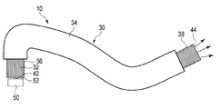
- FIG. 1 shows an embodiment of an illumination device for an endoscope.
- FIG. 2 shows an example (square lattice arrangement pattern) of multiple optical fibers on the incident side end face of the optical bundle fiber of FIG.
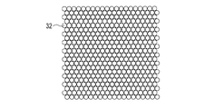
- FIG. 3 shows another example (hexagonal lattice arrangement pattern) of the arrangement pattern of many optical fibers on the incident side end face of the optical bundle fiber of FIG.
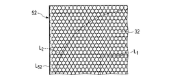
- FIG. 4 shows still another example (honeycomb structure arrangement pattern) of an arrangement pattern of many optical fibers on the incident side end face of the optical bundle fiber of FIG.
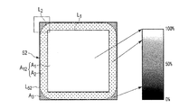
- FIG. 5 schematically shows the luminance distribution on the light emitting surface of the LED light source.
- FIG. 6 shows an LED light source surrounded by an alternate long and short dash line square shown in FIG.
- FIG. 7 is a diagram of an LED light source surrounded by a one-dot chain line square shown in FIG. 5 superimposed on the optical fiber array of the hexagonal lattice arrangement pattern shown in FIG. 3 of the optical fiber bundle in accordance with the conventional idea.
- the upper left corner of the light emitting surface is shown enlarged.
- FIG. 8 is a diagram of an LED light source surrounded by an alternate long and short dash line square shown in FIG. 5 overlaid on the optical fiber array of the honeycomb structure arrangement pattern shown in FIG. 4 of the optical fiber bundle in accordance with the conventional idea.
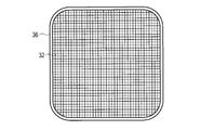
- FIG. 9 schematically shows an incident side end of the optical fiber bundle according to the embodiment.
- FIG. 10 schematically shows an incident side end of an optical fiber bundle according to another embodiment.
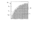
- FIG. 11 shows an enlarged incident side end face of the optical fiber bundle shown in FIG.
- FIG. 12 shows an LED light source surrounded by a dot-and-dash line square shown in FIG. 5 so as to be superimposed on an array of a plurality of optical fibers of the square lattice arrangement pattern shown in FIG. 2 of the optical fiber bundle according to the present embodiment.
- the upper left corner of the light emitting surface is shown enlarged.
- FIG. 13 is a diagram of the LED light source surrounded by the one-dot chain line square shown in FIG.
- FIG. 14 shows an LED light source surrounded by a dot-and-dash line square shown in FIG. 5 so as to overlap with an arrangement of a plurality of optical fibers of the honeycomb structure arrangement pattern shown in FIG. 4 of the optical fiber bundle according to the present embodiment.
- the upper left corner of the light emitting surface is shown enlarged.
- FIG. 1 shows an embodiment of an illumination device 10 for an endoscope (not shown).
- the endoscope illumination apparatus 10 includes an LED light source 50 having a rectangular light emitting surface 52 formed in a substantially flat surface and light emitted from the LED light source 50 in the endoscope.
- the optical fiber bundle 30 led to the distal end portion of the inserted portion is provided.
- the optical fiber bundle 30 is configured by bundling a large number of optical fibers 32, and the large number of optical fibers 32 are accommodated inside a protective tube 34.
- One end portion of the optical fiber bundle 30 is disposed near the LED light source 50, and the other end portion is disposed at a distal end portion of an insertion portion provided in the endoscope.
- the end portion of the optical fiber bundle 30 disposed near the LED light source 50 is referred to as an incident side end portion
- the end portion of the optical fiber bundle 30 disposed at the distal end portion of the insertion portion provided in the endoscope is referred to as an end portion. It will be called the exit side end.
- the end surface of the incident side end portion of the optical fiber bundle 30 is referred to as an incident side end surface
- the end surface of the emission side end portion of the optical fiber bundle 30 is referred to as an emission side end surface.
- a sleeve 36 surrounding a large number of optical fibers 32 is provided at the incident side end of the optical fiber bundle 30.
- the sleeve 36 defines the pattern and contour of the arrangement of a large number of optical fibers 32 on the incident side end face 42 of the optical fiber bundle 30.
- a sleeve 38 surrounding a large number of optical fibers 32 is provided at the exit end of the optical fiber bundle 30.
- the sleeve 38 defines the pattern and contour of the arrangement of a large number of optical fibers 32 on the exit side end face 44 of the optical fiber bundle 30.
- the sleeves 36 and 38 are not disposed inside the protective tube 34.
- the incident side end face 42 of the optical fiber bundle 30 is disposed to face the light emitting face 52 of the LED light source 50.
- the incident side end face 42 of the optical fiber bundle 30 may be arranged in parallel to the light emitting surface 52 with a slight gap from the light emitting surface 52 of the LED light source 50.
- the incident side end surface 42 of the optical fiber bundle 30 may be disposed in contact with the light emitting surface 52 of the LED light source 50.
- the end faces of all the optical fibers 32 may be arranged in a square lattice pattern.
- such an arrangement pattern is referred to as a square lattice arrangement pattern for convenience.
- the multiple optical fibers 32 may be arranged so that the end faces of all the optical fibers 32 are most dense on a plane, that is, in a hexagonal lattice shape.
- a hexagonal lattice arrangement pattern for convenience.
- the multiple optical fibers 32 may be arranged in a honeycomb structure as shown in FIG.
- a honeycomb structure arrangement pattern for convenience.
- the optical fiber bundle 30 having such a honeycomb structure array can be manufactured, for example, by heating and melting a large number of optical fibers 32 arrayed in a hexagonal lattice array.
- the light emitted from the LED light source 50 enters a large number of optical fibers 32 through the incident side end face 42 of the optical fiber bundle 30.
- the light that has entered a large number of optical fibers 32 is guided to the distal end portion of the insertion portion provided in the endoscope by the optical fibers 32, is emitted from the emission side end face 44 of the optical fiber bundle 30, and is provided in the endoscope.
- the periphery of the distal end portion of the insertion portion for example, the front of the distal end portion of the insertion portion is illuminated.
- FIG. 5 schematically shows the luminance distribution on the light emitting surface 52 of the LED light source 50.
- the light emitting surface 52 of the LED light source 50 may be divided into three regions, a central region A 1 , a peripheral region A 2, and a corner region A 3 , according to the light emission luminance.
- Each region of the center region A 1 and the surrounding area A 2 and the corner area A 3 may be considered to be substantially uniform brightness.
- L 1 indicates the boundary line of the outline of the central area A 1
- L 2 indicates the boundary line of the outline of the surrounding area A 2
- L 52 indicates the light emitting surface of the LED light source 50.
- 52 shows the boundary lines of the contours.
- the central region A 1 is a region located at the center of the light emitting surface 52 and has a shape similar to the shape of the light emitting surface 52.
- the corner region A 3 is a region located at the four corners of the light emitting surface 52, and each corner region A 3 has a shape obtained by cutting a 90-degree sector having a radius equal to the length of one side from a square. is doing.
- Surrounding region A 2 is an area which is located around the central area A 1, the light-emitting surface 52 has a shape obtained by cutting the central region A 1 and the four corners region A 3.
- Central area A 1 of the light emitting surface 52 of the LED light source 50 indicating the highest luminance. To 100% the brightness of the central area A 1 as a reference for relative evaluation. The luminance when no light is emitted is set to 0%. In contrast, in the peripheral region A 2 of the light emitting surface 52 located outside the central region A 1, the luminance is about 80%. In contrast, in the corner area A 3 located at the four corners of the light-emitting surface 52 of the LED light source 50, the luminance is at most about 20%.
- the light emitted from the central area A 1 is most suitable as illumination light, and the light emitted from the surrounding area A 2 is not so inferior in brightness as the light emitted from the central area A 1 . It may be used well as illumination light.
- the effective light emission region A 12 is referred to as the effective light emission region A 12.
- light emitted from the corner area A 3, compared to the light emitted from the effective light emitting area A 12 for extremely low luminance is not worthy of use as illuminating light. The reason is as follows.
- optical fiber bundle 30 a large number of optical fibers 32 are accommodated in the protective tube 34 and then fixed to the sleeves 36 and 38 at the incident side end face 42 and the emission side end face 44.
- Many optical fibers 32 accommodated in the protection tube 34 are twisted or shifted in the protection tube 34. Therefore, when the multiple optical fibers 32 are fixed to the sleeves 36 and 38, the positions of the multiple optical fibers 32 on the incident side end face 42 are the same as the positions of the multiple optical fibers 32 on the exit side end face 44.
- the arrangement pattern of the many optical fibers 32 on the incident side end face 42 is not held over the entire length of the optical fiber bundle 30.
- the optical fiber 32 facing the corner region A 3 are distributed in different parts of the exit end face 44, the emission-side end face 44 of the optical fiber bundle 30, a collection of bright light-emitting point A luminance distribution is generated in which dark light emitting points are sparsely present. Such a luminance distribution causes unevenness in illumination.
- FIG. 5 shows an example of an LED light source having a square light emitting surface.
- the shape of the light emitting surface is changed to a rectangle, and similarly, only the corner regions at the four corners are used. It was confirmed that the brightness was remarkably lowered at.
- FIG. 5 shows the luminance distribution of a single LED light source, but even in a configuration in which a plurality of LED light sources are arranged in a matrix, in the entire composite light emitting region constituted by a plurality of LED light sources, Similar to the single light-emitting area of a single LED light source, it was confirmed that the luminance was significantly reduced only in the corner areas of the four corners.
- the shape and size of the outline of the array of the many optical fibers 32 on the incident side end face 42 of the optical fiber bundle 30 are the same as the shape and size of the light emitting surface 52 of the LED light source 50 so far. It was thought that it was good to agree with. 6, 7, and 8 show the light emission of the LED light source 50 that is superimposed on the array of the many optical fibers 32 of the optical fiber bundle 30 in accordance with this idea and that is surrounded by the dashed-dotted square shown in FIG. 5. The upper left corner of the surface is shown enlarged. 6 shows an arrangement of a large number of optical fibers 32 in the square lattice arrangement pattern shown in FIG. 2, and FIG. 7 shows an arrangement of a large number of optical fibers 32 in the hexagonal lattice arrangement pattern shown in FIG. FIG. 8 shows an arrangement of a large number of optical fibers 32 in the honeycomb structure arrangement pattern shown in FIG.
- the optical fiber bundle 30 includes the boundary line L 52 of the contour of the light emitting surface 52 of the LED light source 50 and the contour of the surrounding area A 2 . It is understood that a large number of optical fibers 32 facing the region surrounded by the boundary line L 2 (that is, the corner region A 3 ) are included. Such an optical fiber bundle 30 causes unevenness in illumination by light emitted from the emission side end face 44 of the optical fiber bundle 30 for the reason described above.
- the optical fiber bundle 30 has an outline of an array of a large number of optical fibers 32 on the incident side end face 42 formed in a rounded square shape.
- the optical fiber bundle 30 has an outline of an array of a plurality of optical fibers 32 on the incident side end surface 42, as shown in FIG. Is formed in a rounded square.
- the optical fiber bundle 30 has an outline of an arrangement of a large number of optical fibers 32 on the incident side end surface 42 as shown in FIG. Is formed in a rounded rectangle.
- FIG. 11 shows the incident side end face of the optical fiber bundle 30 shown in FIG. 9 in an enlarged manner.
- 12, 13, and 14 are superimposed on the array of a plurality of optical fibers 32 of the optical fiber bundle 30 according to the present embodiment, and the LED light source 50 surrounded by a one-dot chain line square shown in FIG. 5.
- the upper left corner of the light emitting surface is shown enlarged.
- 12 shows an arrangement of a large number of optical fibers 32 in the square lattice arrangement pattern shown in FIG. 2
- FIG. 13 shows an arrangement of a large number of optical fibers 32 in the hexagonal lattice arrangement pattern shown in FIG.
- FIG. 14 shows an arrangement of a large number of optical fibers 32 in the honeycomb structure arrangement pattern shown in FIG.
- the arrangement of the multiple optical fibers 32 of the optical fiber bundle 30 according to the present embodiment is located inside the boundary line L 2 of the outline of the surrounding area A 2 , do not overlap in the corner region a 3 surrounded by the boundary line L 2 of the contour of the boundary line L 52 of the contour of the light-emitting surface 52 surrounding region a 2 of the LED light source 50. That is, all of the many optical fibers 32 of the optical fiber bundle 30 according to the present embodiment are opposed to the effective light emitting region A 12 of the light emitting surface 52 of the LED light source 50. In other words, the optical fiber bundle 30 according to the present embodiment does not include any optical fiber facing the corner region A 3 of the light emitting surface 52 of the LED light source 50.
- many areas of the contour of the array of optical fiber 32 at the incident side end surface 42 of the optical fiber bundle 30 is substantially equal to a value obtained by subtracting the area of the corner area A 3 from the area of the light emitting surface 52 of the LED light source 50.
- R0.05 (radius 0.05mm) at the corner, R0.1 (radius 0.1mm) at the corner, R0.5 (radius 0.5mm) at the corner, R0.8 (radius 0.8mm) at the corner ) Shows the results for each of the above.
- the brightness is good in the range of R0.05 to R0.5, but the brightness is insufficient in R0.8.
- the illumination is not uneven, but in R0.05, the illumination is uneven.
- corner R0.1 radius 0.1mm
- corner R0.2 radius 0.2mm
- corner R0.8 radius 0.8mm
- corner R1 radius 1mm
- the brightness is good in the range of R0.1 to R0.8, but the brightness is insufficient in R1.
- the range of R0.2 to R1 there is no unevenness in illumination, but in R0.1, unevenness in illumination occurs.
- the brightness is good in the range of R0.05 to R0.5, but the brightness is insufficient in R0.8.
- the illumination is not uneven, but in R0.05, the illumination is uneven.
- the radius of the corners of the contour of the array of optical fibers 32 of the optical fiber bundle 30 is set to a suitable value in accordance with the size and shape of the effective light emitting area A 12 of the light emitting surface 52 of the LED light source 50 to be used It is considered good.
- the radius of the corner of a rounded square is a / 30 to a with respect to the length a of one side
- the radius of the corner of a rounded rectangle is a length a of the short side. It is good to set to the range of / 6.
Landscapes
- Health & Medical Sciences (AREA)
- Life Sciences & Earth Sciences (AREA)
- Surgery (AREA)
- Physics & Mathematics (AREA)
- Optics & Photonics (AREA)
- Biomedical Technology (AREA)
- Animal Behavior & Ethology (AREA)
- Radiology & Medical Imaging (AREA)
- Nuclear Medicine, Radiotherapy & Molecular Imaging (AREA)
- Engineering & Computer Science (AREA)
- Biophysics (AREA)
- Heart & Thoracic Surgery (AREA)
- Medical Informatics (AREA)
- Molecular Biology (AREA)
- Pathology (AREA)
- General Health & Medical Sciences (AREA)
- Public Health (AREA)
- Veterinary Medicine (AREA)
- General Physics & Mathematics (AREA)
- Optical Fibers, Optical Fiber Cores, And Optical Fiber Bundles (AREA)
- Instruments For Viewing The Inside Of Hollow Bodies (AREA)
- Endoscopes (AREA)
Abstract
内視鏡のための照明装置(10)は、略平面に形成された方形の発光面(52)を有するLED光源(50)と、このLED光源(50)から発せられる光を内視鏡に備えられる挿入部の先端部に導く光ファイババンドル(30)を備えている。光ファイババンドル(30)は、多数の光ファイバ(32)を束ねて構成されている。光ファイババンドル(30)は、LED光源(50)の発光面(52)に対向して配置される入射側端面(42)における多数の光ファイバ(32)の配列の輪郭が角丸方形に形成されている。
Description
本発明は、光ファイババンドルを用いた内視鏡のための照明装置に関する。
内視鏡のための照明装置として、光ファイババンドルを用いたものが知られている。このような照明装置において、LED光源を用いて十分な光量を得るためには、LED光源の発光面に対して光ファイババンドルの端面が対向して配置されていること、また、光ファイババンドルの多数の光ファイバの配列の輪郭がLED光源の発光面の輪郭と同じ形状と大きさを有していることが望ましいとされている。
この目的に沿った光ファイババンドルの一例は、たとえば特開2001-343536号公報に開示されている。
内視鏡のための照明においては、十分な光量に加えて、内視鏡の観察性能を低下させる要因の一つである照明ムラがないことが要求される。
しかし、上記のように構成された光ファイババンドルを用いた内視鏡のための照明装置においては、十分な光量が得られるものの、その照明にはムラが発生しており、さらなる改善が望まれている。
本発明の目的は、内視鏡のための照明の改善に向けられており、内視鏡のための照明装置に用いられる照明のムラの発生を低減する光ファイババンドルを提供することである。
本発明は、多数の光ファイバを束ねて構成されている光ファイババンドルであり、一方の端面における多数の光ファイバの配列の輪郭が角丸方形に形成されている。
本発明によれば、内視鏡のための照明装置に用いられる照明のムラの発生を低減する光ファイババンドルが提供される。
以下、図面を参照しながら本発明の実施形態について説明する。
図1は、内視鏡(図示せず)のための照明装置10の一実施形態を示している。この内視鏡の照明装置10は、図1に示されるように、略平面に形成された方形の発光面52を有するLED光源50と、このLED光源50から発せられる光を内視鏡に備えられる挿入部の先端部に導く光ファイババンドル30を備えている。
光ファイババンドル30は、多数の光ファイバ32を束ねて構成されており、多数の光ファイバ32は保護チューブ34の内部に収容されている。光ファイババンドル30の一方の端部は、LED光源50の近くに配置され、他方の端部は、内視鏡に備えられる挿入部の先端部に配置される。以下では、LED光源50の近くに配置される光ファイババンドル30の端部を入射側端部と呼び、内視鏡に備えられる挿入部の先端部に配置される光ファイババンドル30の端部を射出側端部と呼ぶことにする。また、光ファイババンドル30の入射側端部の端面を入射側端面と呼び、光ファイババンドル30の射出側端部の端面を射出側端面と呼ぶことにする。
光ファイババンドル30の入射側端部には、多数の光ファイバ32を取り巻いているスリーブ36が設けられている。このスリーブ36は、光ファイババンドル30の入射側端面42における多数の光ファイバ32の配列のパターンと輪郭を定めている。また、光ファイババンドル30の射出側端部には、多数の光ファイバ32を取り巻いているスリーブ38が設けられている。このスリーブ38は、光ファイババンドル30の射出側端面44における多数の光ファイバ32の配列のパターンと輪郭を定めている。スリーブ36,38は、保護チューブ34の内部に配置されていない。
光ファイババンドル30の入射側端面42は、LED光源50の発光面52に対向して配置される。一例では、光ファイババンドル30の入射側端面42は、LED光源50の発光面52からわずかな隙間をおいて、発光面52に平行に配置されていてよい。別の例では、光ファイババンドル30の入射側端面42は、LED光源50の発光面52に接触して配置されていてもよい。
多数の光ファイバ32は、一例では、図2に示されるように、すべての光ファイバ32の端面が正方格子状に配列されていてよい。以下では、このような配列パターンを、便宜上、正方格子配列パターンと呼ぶことにする。
多数の光ファイバ32は、別の例では、図3に示されるように、すべての光ファイバ32の端面が、平面上において最も密になるように、すなわち六方格子状に配列されていてよい。以下では、このような配列パターンを、便宜上、六方格子配列パターンと呼ぶことにする。
多数の光ファイバ32は、また別の例では、図4に示されるように、ハニカム構造状に配列されていてよい。以下では、このような配列パターンを、便宜上、ハニカム構造配列パターンと呼ぶことにする。このようなハニカム構造配列の光ファイババンドル30は、たとえば、六方格子配列に配列された多数の光ファイバ32を加熱して溶融させることによって作製され得る。
図1に示された内視鏡の照明装置10において、LED光源50から発せられた光は、光ファイババンドル30の入射側端面42を通って、多数の光ファイバ32に進入する。多数の光ファイバ32に進入した光は、光ファイバ32によって内視鏡に備えられる挿入部の先端部にまで導かれ、光ファイババンドル30の射出側端面44から射出され、内視鏡に備えられる挿入部の先端部の周辺たとえば挿入部の先端部の前方を照明する。
本発明者らは、このような内視鏡の照明装置10に一般に使用されるLED光源50において、その発光面52の輝度分布にムラがあることに気づいた。図5は、LED光源50の発光面52における輝度分布を概略的に示している。LED光源50の発光面52は、図5に示されるように、発光輝度に従って、中央領域A1と周囲領域A2と角部領域A3の三つの領域に分けて考えられてよい。中央領域A1と周囲領域A2と角部領域A3の各領域内は、ほぼ均一な輝度であると見なされてよい。図5において、L1は、中央領域A1の輪郭の境界線を示しており、L2は、周囲領域A2の輪郭の境界線を示しており、L52は、LED光源50の発光面52の輪郭の境界線を示している。
中央領域A1は、発光面52の中央に位置している領域であり、発光面52の形状に相似な形状をしている。角部領域A3は、発光面52の四隅に位置している領域であり、各角部領域A3は、正方形から、その一辺の長さに等しい半径の90度の扇形を切り取った形状をしている。周囲領域A2は、中央領域A1の周囲に位置している領域であり、発光面52から、中央領域A1と四つの角部領域A3を切り取った形状をしている。
LED光源50の発光面52の中央領域A1は最も高い輝度を示す。中央領域A1の輝度を相対評価の基準として100%とする。また無発光時の輝度を0%とする。これに対して、中央領域A1の外側に位置する発光面52の周囲領域A2では、その輝度は80%程度である。これに対して、LED光源50の発光面52の四隅に位置する角部領域A3では、その輝度はせいぜい20%程度である。
中央領域A1と周囲領域A2と角部領域A3の面積比は、たとえば、中央領域A1は、発光面52の面積の60%程度、周囲領域A2は、発光面52の面積の38%程度、角部領域A3は、発光面52の面積の2%程度であってよい。
図5において、中央領域A1から発せられる光は、照明光として最も適切であり、また周囲領域A2から発せられる光は、中央領域A1から発せられる光と比べて輝度がそれほど劣らないので、照明光として良好に使用されてよい。以下では、必要に応じて、中央領域A1と周囲領域A2を合わせて有効発光領域A12と呼ぶことにする。これに対して、角部領域A3から発せられる光は、有効発光領域A12から発せられる光に比べると輝度が著しく低いため、照明光として使用するにはふさわしくない。その理由は、次の通りである。
光ファイババンドル30において、多数の光ファイバ32は、保護チューブ34に収容された後、入射側端面42と射出側端面44とにおいてスリーブ36,38に固定される。保護チューブ34に収容された多数の光ファイバ32は、保護チューブ34内において捩じれたりずれたりする。このため、多数の光ファイバ32がスリーブ36,38に固定される際、入射側端面42における多数の光ファイバ32のそれぞれの位置は、射出側端面44における多数の光ファイバ32のそれぞれの位置とは一般に相違する。つまり、入射側端面42における多数の光ファイバ32の配列パターンは、光ファイババンドル30の全長にわたって保持されているわけではない。このため、角部領域A3に対向している光ファイバ32が射出側端面44の様々な部分に分布している場合、光ファイババンドル30の射出側端面44においては、明るい発光点の集まりの中に暗い発光点がまばらに存在するといった輝度分布が生じる。このような輝度分布は、照明にムラを生じさせる原因になる。
図5は、正方形の発光面をもつLED光源の例を示しているが、長方形の発光面をもつLED光源では、発光面の形状が長方形に変わるほか、やはり同様に、四隅の角部領域だけにおいて輝度が著しく低下することが確認された。
また図5は、単一のLED光源の輝度分布を示しているが、複数のLED光源がマトリックス状に配置された構成においても、複数のLED光源によって構成された複合の発光領域の全体において、単一のLED光源の単一の発光領域と同様に、四隅の角部領域だけにおいて輝度が著しく低下することが確認された。
図1に示される照明装置10において、これまで、光ファイババンドル30の入射側端面42における多数の光ファイバ32の配列の輪郭の形状と大きさは、LED光源50の発光面52の形状と大きさと一致しているのがよいと考えられていた。図6と図7と図8は、この考えに則った光ファイババンドル30の多数の光ファイバ32の配列に重ねて、図5に示された一点鎖線の正方形で囲まれたLED光源50の発光面の左上隅の部分を拡大して示している。図6は、図2に示された正方格子配列パターンの多数の光ファイバ32の配列を示しており、図7は、図3に示された六方格子配列パターンの多数の光ファイバ32の配列を示しており、図8は、図4に示されたハニカム構造配列パターンの多数の光ファイバ32の配列を示している。
図6と図7と図8から、それらの図に示されたいずれの例においても、光ファイババンドル30は、LED光源50の発光面52の輪郭の境界線L52と周囲領域A2の輪郭の境界線L2とで囲まれる領域(すなわち角部領域A3)に対向する多くの光ファイバ32を含んでいることが理解される。このような光ファイババンドル30は、前述した理由から、光ファイババンドル30の射出側端面44から射出される光による照明にムラを生じさせてしまう。
図9と図10は、本実施形態の照明装置10における光ファイババンドル30の入射側端部を模式的に示している。本実施形態における照明装置10では、光ファイババンドル30は、図9と図10に示されるように、入射側端面42における多数の光ファイバ32の配列の輪郭が角丸方形に形成されている。たとえば、LED光源50が正方形の発光面52を有している構成に対しては、光ファイババンドル30は、図9に示されるように、入射側端面42における多数の光ファイバ32の配列の輪郭が角丸正方形に形成されている。また、LED光源50が長方形の発光面52を有している構成に対しては、光ファイババンドル30は、図10に示されるように、入射側端面42における多数の光ファイバ32の配列の輪郭が角丸長方形に形成されている。
図11は、図9に示された光ファイババンドル30の入射側端面を拡大して示している。また、図12と図13と図14は、本実施形態による光ファイババンドル30の多数の光ファイバ32の配列に重ねて、図5に示された一点鎖線の正方形で囲まれたLED光源50の発光面の左上隅の部分を拡大して示している。図12は、図2に示された正方格子配列パターンの多数の光ファイバ32の配列を示しており、図13は、図3に示された六方格子配列パターンの多数の光ファイバ32の配列を示しており、図14は、図4に示されたハニカム構造配列パターンの多数の光ファイバ32の配列を示している。
図12と図13と図14のいずれにおいても、本実施形態による光ファイババンドル30の多数の光ファイバ32の配列は、周囲領域A2の輪郭の境界線L2の内側に位置しており、LED光源50の発光面52の輪郭の境界線L52と周囲領域A2の輪郭の境界線L2とで囲まれる角部領域A3に重なっていない。つまり、本実施形態による光ファイババンドル30の多数の光ファイバ32はすべて、LED光源50の発光面52の有効発光領域A12に対向している。言い換えれば、本実施形態による光ファイババンドル30は、LED光源50の発光面52の角部領域A3に対向する光ファイバをまったく含んでいない。
また別の観点からとらえるならば、光ファイババンドル30の入射側端面42における多数の光ファイバ32の配列の形状と大きさは、LED光源50の発光面52の有効発光領域A12の形状と大きさと同じであると言える。したがって、光ファイババンドル30の入射側端面42における多数の光ファイバ32の配列の輪郭の面積は、LED光源50の発光面52の面積から角部領域A3の面積を減算した値にほぼ等しい。
このため、光ファイババンドル30の射出側端面44から射出される光による照明に、前述した理由に起因するムラは生じない。
以下に、いくつかの条件において、LED光源50の発光面52から発せられた光を光ファイババンドル30によって内視鏡に備えられる挿入部の先端部にまで導光する実験をおこなった結果を示す。実験には、六方格子配列パターンの光ファイバ32を有する光ファイババンドル30を用い、光ファイバ32の輪郭の角部の半径の違いに対する結果の違いを評価した。実験結果の評価は、明るさの良否と照明ムラの良否でおこなった。
下記の表1は、3mm×3mmの大きさの発光面52をもつLED光源50に対して、光ファイババンドル30の光ファイバ32の配列の輪郭は、一辺a=3mmの角丸正方形であり、角部のR0.05(半径0.05mm)、角部のR0.1(半径0.1mm)、角部のR0.5(半径0.5mm)、角部のR0.8(半径0.8mm)のそれぞれについての結果を示している。

表1から次のことが言える。R0.05ないしR0.5の範囲では明るさは良好であるが、R0.8では明るさが不足する。一方、R0.1ないしR0.8の範囲では照明にムラは生じないが、R0.05では照明にムラが生じる。
下記の表2は、5mm×5mmの大きさの発光面52をもつLED光源50に対して、光ファイババンドル30の光ファイバ32の配列の輪郭は、一辺a=5mmの角丸正方形であり、角部のR0.1(半径0.1mm)、角部のR0.2(半径0.2mm)、角部のR0.8(半径0.8mm)、角部のR1(半径1mm)のそれぞれについての結果を示している。

表2から次のことが言える。R0.1ないしR0.8の範囲では明るさは良好であるが、R1では明るさが不足する。一方、R0.2ないしR1の範囲では照明にムラは生じないが、R0.1では照明にムラが生じる。
下記の表3は、3mm×5mmの大きさの発光面52をもつLED光源50に対して、光ファイババンドル30の光ファイバ32の配列の輪郭は、短辺a=3mm、長辺b=5mmの角丸長方形であり、角部のR0.05(半径0.05mm)、角部のR0.1(半径0.1mm)、角部のR0.5(半径0.5mm)、角部のR0.8(半径0.8mm)、角部のR1(半径1mm)のそれぞれについての結果を示している。

表3から次のことが言える。R0.05ないしR0.5の範囲では明るさは良好であるが、R0.8では明るさが不足する。一方、R0.1ないしR0.8の範囲では照明にムラは生じないが、R0.05では照明にムラが生じる。
以上から、次のように考えることができる。光ファイババンドル30の光ファイバ32の配列の輪郭の角部の半径が大きすぎると、LED光源50の発光面52の有効発光領域A12から発せられた光の使用率が低下するために明るさに不足が生じる。反対に、光ファイババンドル30の光ファイバ32の配列の輪郭の角部の半径が小さすぎると、LED光源50の発光面52の角部領域A3から発せられた光が光ファイババンドル30に進入するために照明にムラが生じる。
したがって、光ファイババンドル30の光ファイバ32の配列の輪郭の角部の半径は、使用するLED光源50の発光面52の有効発光領域A12の大きさと形状に合わせて適当な数値に設定されるとよいと考えられる。
たとえば、角丸正方形の角部の半径は、その一辺の長さaに対して、また、角丸長方形の角部の半径は、その短辺の長さaに対して、a/30ないしa/6の範囲に設定されているとよい。
Claims (10)
- 多数の光ファイバを束ねて構成された光ファイババンドルにおいて、一方の端面における前記多数の光ファイバの配列の輪郭が角丸方形に形成されていることを特徴とする光ファイババンドル。
- 前記多数の光ファイバの配列の輪郭が角丸正方形に形成されていることを特徴とする、請求項1に記載の光ファイババンドル。
- 前記多数の光ファイバの配列の輪郭が角丸長方形に形成されていることを特徴とする、請求項1に記載の光ファイババンドル。
- 前記角丸方形の辺のうち最も短い辺の長さをaとしたとき、前記角丸方形の角部の半径がa/30ないしa/6の範囲に設定されていることを特徴とする、請求項1に記載の光ファイババンドル。
- 略平面に形成された方形の発光面を有するLED光源と、このLED光源から発せられる光を内視鏡に備えられる挿入部の先端部に導く光ファイババンドルを備えた内視鏡の照明装置において、
前記光ファイババンドルは、多数の光ファイバを束ねて構成されており、前記光ファイババンドルは、一方の端面が、前記LED光源の前記発光面に対向して配置され、前記光ファイババンドルの前記端面における前記多数の光ファイバの配列の輪郭が角丸方形に形成されていることを特徴とする内視鏡のための照明装置。 - 前記多数の光ファイバの配列の輪郭が角丸正方形に形成されていることを特徴とする、請求項5に記載の照明装置。
- 前記多数の光ファイバの配列の輪郭が角丸長方形に形成されていることを特徴とする、請求項5に記載の照明装置。
- 前記角丸方形の辺のうち最も短い辺の長さをaとしたとき、前記角丸方形の角部の半径がa/30ないしa/6の範囲に設定されていることを特徴とする、請求項5に記載の照明装置。
- 前記光ファイババンドルの前記端面における前記多数の光ファイバの配列の輪郭の面積は、前記LED光源の前記発光面の面積から、発光輝度が低い前記発光面の角部の面積を減算した値にほぼ等しいことを特徴とする、請求項5に記載の照明装置。
- 前記光ファイババンドルの前記端面は、前記LED光源の前記発光面に接触して配置されていることを特徴とする、請求項9に記載の照明装置。
Priority Applications (1)
| Application Number | Priority Date | Filing Date | Title |
|---|---|---|---|
| CN201690000224.5U CN206362970U (zh) | 2015-06-26 | 2016-03-25 | 内窥镜用的照明装置 |
Applications Claiming Priority (2)
| Application Number | Priority Date | Filing Date | Title |
|---|---|---|---|
| JP2015-128763 | 2015-06-26 | ||
| JP2015128763A JP2018134117A (ja) | 2015-06-26 | 2015-06-26 | 光ファイババンドルおよびそれを用いた内視鏡のための照明装置 |
Publications (1)
| Publication Number | Publication Date |
|---|---|
| WO2016208245A1 true WO2016208245A1 (ja) | 2016-12-29 |
Family
ID=57585511
Family Applications (1)
| Application Number | Title | Priority Date | Filing Date |
|---|---|---|---|
| PCT/JP2016/059736 Ceased WO2016208245A1 (ja) | 2015-06-26 | 2016-03-25 | 光ファイババンドルおよびそれを用いた内視鏡のための照明装置 |
Country Status (3)
| Country | Link |
|---|---|
| JP (1) | JP2018134117A (ja) |
| CN (1) | CN206362970U (ja) |
| WO (1) | WO2016208245A1 (ja) |
Citations (8)
| Publication number | Priority date | Publication date | Assignee | Title |
|---|---|---|---|---|
| JPH04182691A (ja) * | 1990-11-17 | 1992-06-30 | Access:Kk | 拡大表示装置 |
| JP2007148418A (ja) * | 2001-08-31 | 2007-06-14 | Smith & Nephew Inc | 固体光源 |
| JP2008011991A (ja) * | 2006-07-04 | 2008-01-24 | Olympus Medical Systems Corp | 内視鏡 |
| JP2009212287A (ja) * | 2008-03-04 | 2009-09-17 | Stanley Electric Co Ltd | Ledパッケージ |
| WO2012002029A1 (ja) * | 2010-07-01 | 2012-01-05 | シャープ株式会社 | 照明装置、表示装置、テレビ受信装置およびled光源 |
| JP2013051375A (ja) * | 2011-08-31 | 2013-03-14 | Nichia Chem Ind Ltd | 発光装置 |
| US20140153880A1 (en) * | 2012-11-30 | 2014-06-05 | General Electric Company | Device and method for bundling optical fibers |
| JP2014229759A (ja) * | 2013-05-23 | 2014-12-08 | 日亜化学工業株式会社 | 発光装置 |
-
2015
- 2015-06-26 JP JP2015128763A patent/JP2018134117A/ja active Pending
-
2016
- 2016-03-25 WO PCT/JP2016/059736 patent/WO2016208245A1/ja not_active Ceased
- 2016-03-25 CN CN201690000224.5U patent/CN206362970U/zh not_active Expired - Fee Related
Patent Citations (8)
| Publication number | Priority date | Publication date | Assignee | Title |
|---|---|---|---|---|
| JPH04182691A (ja) * | 1990-11-17 | 1992-06-30 | Access:Kk | 拡大表示装置 |
| JP2007148418A (ja) * | 2001-08-31 | 2007-06-14 | Smith & Nephew Inc | 固体光源 |
| JP2008011991A (ja) * | 2006-07-04 | 2008-01-24 | Olympus Medical Systems Corp | 内視鏡 |
| JP2009212287A (ja) * | 2008-03-04 | 2009-09-17 | Stanley Electric Co Ltd | Ledパッケージ |
| WO2012002029A1 (ja) * | 2010-07-01 | 2012-01-05 | シャープ株式会社 | 照明装置、表示装置、テレビ受信装置およびled光源 |
| JP2013051375A (ja) * | 2011-08-31 | 2013-03-14 | Nichia Chem Ind Ltd | 発光装置 |
| US20140153880A1 (en) * | 2012-11-30 | 2014-06-05 | General Electric Company | Device and method for bundling optical fibers |
| JP2014229759A (ja) * | 2013-05-23 | 2014-12-08 | 日亜化学工業株式会社 | 発光装置 |
Also Published As
| Publication number | Publication date |
|---|---|
| JP2018134117A (ja) | 2018-08-30 |
| CN206362970U (zh) | 2017-07-28 |
Similar Documents
| Publication | Publication Date | Title |
|---|---|---|
| US9753270B2 (en) | Illumination device | |
| JP2015016022A (ja) | 照明装置 | |
| JP6103820B2 (ja) | 内視鏡用照明光学系および内視鏡 | |
| US20110257484A1 (en) | Light source device and endoscope apparatus using the same | |
| JP6430104B2 (ja) | 照明装置 | |
| TW201307918A (zh) | 具有解耦部分之光導引件及收集解耦光線之屏蔽件 | |
| JP2002186578A5 (ja) | ||
| CN106413519B (zh) | 光源模组和内窥镜用光源系统 | |
| US20050152028A1 (en) | Illumination device for a microscope | |
| TW200901116A (en) | Illumination apparatus | |
| CN104425686A (zh) | 照明装置 | |
| JPWO2015107844A1 (ja) | 内視鏡装置 | |
| WO2014189091A1 (ja) | 内視鏡 | |
| TWM521195U (zh) | 導光材、背光模組和顯示裝置 | |
| WO2016208245A1 (ja) | 光ファイババンドルおよびそれを用いた内視鏡のための照明装置 | |
| WO2016027634A1 (ja) | 内視鏡装置 | |
| US9223079B2 (en) | Light guide plate and backlight module | |
| DE602006012433D1 (de) | Anzeige von Kontrollleuchten in Nachtsichtgeräten, die einen faseroptischen Bildschirm verwenden | |
| TWI528059B (zh) | 導光板 | |
| CN113741029B (zh) | 虚像投影装置 | |
| US20070291504A1 (en) | Fused fiber array optics for led | |
| WO2020039622A1 (ja) | 内視鏡装置 | |
| JP5148386B2 (ja) | 発光表示装置 | |
| JP2012244417A (ja) | 読取装置 | |
| JP2016099625A5 (ja) |
Legal Events
| Date | Code | Title | Description |
|---|---|---|---|
| 121 | Ep: the epo has been informed by wipo that ep was designated in this application |
Ref document number: 16814016 Country of ref document: EP Kind code of ref document: A1 |
|
| NENP | Non-entry into the national phase |
Ref country code: DE |
|
| NENP | Non-entry into the national phase |
Ref country code: JP |
|
| 122 | Ep: pct application non-entry in european phase |
Ref document number: 16814016 Country of ref document: EP Kind code of ref document: A1 |