WO2016208207A1 - 三次元計測装置 - Google Patents
三次元計測装置 Download PDFInfo
- Publication number
- WO2016208207A1 WO2016208207A1 PCT/JP2016/050552 JP2016050552W WO2016208207A1 WO 2016208207 A1 WO2016208207 A1 WO 2016208207A1 JP 2016050552 W JP2016050552 W JP 2016050552W WO 2016208207 A1 WO2016208207 A1 WO 2016208207A1
- Authority
- WO
- WIPO (PCT)
- Prior art keywords
- luminance
- measurement
- light pattern
- image data
- gain
- Prior art date
- Legal status (The legal status is an assumption and is not a legal conclusion. Google has not performed a legal analysis and makes no representation as to the accuracy of the status listed.)
- Ceased
Links
Images




Classifications
-
- G—PHYSICS
- G01—MEASURING; TESTING
- G01B—MEASURING LENGTH, THICKNESS OR SIMILAR LINEAR DIMENSIONS; MEASURING ANGLES; MEASURING AREAS; MEASURING IRREGULARITIES OF SURFACES OR CONTOURS
- G01B11/00—Measuring arrangements characterised by the use of optical techniques
- G01B11/24—Measuring arrangements characterised by the use of optical techniques for measuring contours or curvatures
- G01B11/25—Measuring arrangements characterised by the use of optical techniques for measuring contours or curvatures by projecting a pattern, e.g. one or more lines, moiré fringes on the object
- G01B11/2513—Measuring arrangements characterised by the use of optical techniques for measuring contours or curvatures by projecting a pattern, e.g. one or more lines, moiré fringes on the object with several lines being projected in more than one direction, e.g. grids, patterns
-
- G—PHYSICS
- G01—MEASURING; TESTING
- G01B—MEASURING LENGTH, THICKNESS OR SIMILAR LINEAR DIMENSIONS; MEASURING ANGLES; MEASURING AREAS; MEASURING IRREGULARITIES OF SURFACES OR CONTOURS
- G01B11/00—Measuring arrangements characterised by the use of optical techniques
- G01B11/02—Measuring arrangements characterised by the use of optical techniques for measuring length, width or thickness
- G01B11/06—Measuring arrangements characterised by the use of optical techniques for measuring length, width or thickness for measuring thickness ; e.g. of sheet material
- G01B11/0608—Height gauges
-
- G—PHYSICS
- G01—MEASURING; TESTING
- G01B—MEASURING LENGTH, THICKNESS OR SIMILAR LINEAR DIMENSIONS; MEASURING ANGLES; MEASURING AREAS; MEASURING IRREGULARITIES OF SURFACES OR CONTOURS
- G01B11/00—Measuring arrangements characterised by the use of optical techniques
- G01B11/24—Measuring arrangements characterised by the use of optical techniques for measuring contours or curvatures
- G01B11/25—Measuring arrangements characterised by the use of optical techniques for measuring contours or curvatures by projecting a pattern, e.g. one or more lines, moiré fringes on the object
-
- G—PHYSICS
- G01—MEASURING; TESTING
- G01B—MEASURING LENGTH, THICKNESS OR SIMILAR LINEAR DIMENSIONS; MEASURING ANGLES; MEASURING AREAS; MEASURING IRREGULARITIES OF SURFACES OR CONTOURS
- G01B11/00—Measuring arrangements characterised by the use of optical techniques
- G01B11/24—Measuring arrangements characterised by the use of optical techniques for measuring contours or curvatures
- G01B11/25—Measuring arrangements characterised by the use of optical techniques for measuring contours or curvatures by projecting a pattern, e.g. one or more lines, moiré fringes on the object
- G01B11/2518—Projection by scanning of the object
- G01B11/2527—Projection by scanning of the object with phase change by in-plane movement of the patern
-
- G—PHYSICS
- G01—MEASURING; TESTING
- G01N—INVESTIGATING OR ANALYSING MATERIALS BY DETERMINING THEIR CHEMICAL OR PHYSICAL PROPERTIES
- G01N21/00—Investigating or analysing materials by the use of optical means, i.e. using sub-millimetre waves, infrared, visible or ultraviolet light
- G01N21/84—Systems specially adapted for particular applications
- G01N21/88—Investigating the presence of flaws or contamination
- G01N21/95—Investigating the presence of flaws or contamination characterised by the material or shape of the object to be examined
- G01N21/956—Inspecting patterns on the surface of objects
-
- G—PHYSICS
- G06—COMPUTING OR CALCULATING; COUNTING
- G06T—IMAGE DATA PROCESSING OR GENERATION, IN GENERAL
- G06T7/00—Image analysis
- G06T7/0002—Inspection of images, e.g. flaw detection
- G06T7/0004—Industrial image inspection
- G06T7/001—Industrial image inspection using an image reference approach
-
- G—PHYSICS
- G06—COMPUTING OR CALCULATING; COUNTING
- G06T—IMAGE DATA PROCESSING OR GENERATION, IN GENERAL
- G06T7/00—Image analysis
- G06T7/50—Depth or shape recovery
- G06T7/521—Depth or shape recovery from laser ranging, e.g. using interferometry; from the projection of structured light
-
- G—PHYSICS
- G06—COMPUTING OR CALCULATING; COUNTING
- G06T—IMAGE DATA PROCESSING OR GENERATION, IN GENERAL
- G06T7/00—Image analysis
- G06T7/60—Analysis of geometric attributes
-
- H—ELECTRICITY
- H05—ELECTRIC TECHNIQUES NOT OTHERWISE PROVIDED FOR
- H05K—PRINTED CIRCUITS; CASINGS OR CONSTRUCTIONAL DETAILS OF ELECTRIC APPARATUS; MANUFACTURE OF ASSEMBLAGES OF ELECTRICAL COMPONENTS
- H05K13/00—Apparatus or processes specially adapted for manufacturing or adjusting assemblages of electric components
- H05K13/08—Monitoring manufacture of assemblages
- H05K13/081—Integration of optical monitoring devices in assembly lines; Processes using optical monitoring devices specially adapted for controlling devices or machines in assembly lines
- H05K13/0817—Monitoring of soldering processes
-
- G—PHYSICS
- G01—MEASURING; TESTING
- G01N—INVESTIGATING OR ANALYSING MATERIALS BY DETERMINING THEIR CHEMICAL OR PHYSICAL PROPERTIES
- G01N21/00—Investigating or analysing materials by the use of optical means, i.e. using sub-millimetre waves, infrared, visible or ultraviolet light
- G01N21/84—Systems specially adapted for particular applications
- G01N21/88—Investigating the presence of flaws or contamination
- G01N21/95—Investigating the presence of flaws or contamination characterised by the material or shape of the object to be examined
- G01N21/956—Inspecting patterns on the surface of objects
- G01N2021/95638—Inspecting patterns on the surface of objects for PCB's
- G01N2021/95646—Soldering
-
- G—PHYSICS
- G06—COMPUTING OR CALCULATING; COUNTING
- G06T—IMAGE DATA PROCESSING OR GENERATION, IN GENERAL
- G06T2200/00—Indexing scheme for image data processing or generation, in general
- G06T2200/04—Indexing scheme for image data processing or generation, in general involving 3D image data
-
- G—PHYSICS
- G06—COMPUTING OR CALCULATING; COUNTING
- G06T—IMAGE DATA PROCESSING OR GENERATION, IN GENERAL
- G06T2207/00—Indexing scheme for image analysis or image enhancement
- G06T2207/10—Image acquisition modality
- G06T2207/10141—Special mode during image acquisition
- G06T2207/10152—Varying illumination
-
- G—PHYSICS
- G06—COMPUTING OR CALCULATING; COUNTING
- G06T—IMAGE DATA PROCESSING OR GENERATION, IN GENERAL
- G06T2207/00—Indexing scheme for image analysis or image enhancement
- G06T2207/30—Subject of image; Context of image processing
- G06T2207/30108—Industrial image inspection
- G06T2207/30141—Printed circuit board [PCB]
-
- G—PHYSICS
- G06—COMPUTING OR CALCULATING; COUNTING
- G06T—IMAGE DATA PROCESSING OR GENERATION, IN GENERAL
- G06T2207/00—Indexing scheme for image analysis or image enhancement
- G06T2207/30—Subject of image; Context of image processing
- G06T2207/30108—Industrial image inspection
- G06T2207/30148—Semiconductor; IC; Wafer
-
- G—PHYSICS
- G06—COMPUTING OR CALCULATING; COUNTING
- G06T—IMAGE DATA PROCESSING OR GENERATION, IN GENERAL
- G06T2207/00—Indexing scheme for image analysis or image enhancement
- G06T2207/30—Subject of image; Context of image processing
- G06T2207/30108—Industrial image inspection
- G06T2207/30152—Solder
Definitions
- the present invention relates to a three-dimensional measurement apparatus that performs three-dimensional measurement using a phase shift method.
- a printed circuit board has an electrode pattern on a base substrate made of glass epoxy resin, and the surface is protected by a resist film.
- cream solder is first printed at a predetermined position on the electrode pattern that is not protected by a resist film.
- an electronic component is temporarily fixed on the printed circuit board based on the viscosity of the cream solder.
- the printed circuit board is guided to a reflow furnace, and soldering is performed through a predetermined reflow process.
- the object to be measured (in this case, the printed circuit board) is irradiated by the irradiation means. And it observes using the imaging means which has arrange
- the imaging means a CCD camera or the like including a lens and an imaging element is used.
- the light intensity (luminance) I of each coordinate (pixel) on the image data imaged by the imaging means is given by the following equation (T1).
- I f ⁇ sin ⁇ + e (T1) Where f: gain, e: offset, and ⁇ : phase of the light pattern.
- the phase of the light pattern is changed in, for example, four stages ( ⁇ + 0, ⁇ + 90 °, ⁇ + 180 °, ⁇ + 270 °), and intensity distributions I 0 , I 1 , I 2 corresponding thereto.
- I 3 is taken in, f (gain) and e (offset) are canceled based on the following equation (T2), and the phase ⁇ is obtained.
- the background region there are various colors around the printed portion of the cream solder on the printed circuit board (hereinafter referred to as the background region). This is because various colors are used for the glass epoxy resin and the resist film. Then, for example, in a relatively dark background region such as black, the contrast of the image data captured by the imaging unit is reduced. That is, the light / dark difference (luminance difference) of the light pattern is reduced in the image data. This may make it difficult to measure the height of the background area.
- a height reference in the substrate.
- the background area cannot be properly used as the height reference plane, there is a possibility that a height reference cannot be taken in the substrate.
- the phase of the light pattern to be irradiated is changed in four steps (or three steps), and four (or three) images are taken. There is a need to.
- the first light pattern having the first luminance is irradiated, and its phase is changed in four steps (or three steps).
- the luminance is changed, the second light pattern having the second luminance is irradiated, and the phase is changed in four steps (or three steps).
- four (or three) images are captured, and each image is captured four times (or three times) under the light pattern of each luminance, for a total of eight times (or six times). There was a risk of a significant increase.
- the time required for measuring the one printed circuit board is further several times that time. Therefore, further shortening of the measurement time is required.
- the present invention has been made in view of the above circumstances, and an object thereof is to perform three-dimensional measurement capable of realizing higher-precision measurement in a shorter time when performing three-dimensional measurement using the phase shift method. To provide an apparatus.
- Means 1 A light source that emits predetermined light; and a grating that converts the light from the light source into a light pattern having a striped light intensity distribution.
- the light pattern is divided into at least a first measurement target region and a second measurement target region.
- An irradiation means capable of irradiating the object to be measured;
- Brightness control means capable of changing the brightness of light emitted from the light source;
- Phase control means for controlling the transfer or switching of the grating and capable of changing the phase of the light pattern irradiated from the irradiation means in a plurality of ways;
- Imaging means capable of imaging reflected light from the object to be measured irradiated with the light pattern;
- Image processing means capable of performing three-dimensional measurement of the object to be measured by a phase shift method based on image data picked up by the image pickup means;
- the image processing means includes The first light pattern having the first luminance corresponding to the first measurement target region is irradiated with a predetermined number (for example, three or four) of phases and imaged based on the predetermined number of image data.
- First measurement means for performing three-dimensional measurement related to the measurement target region;
- a relationship grasping means for grasping a relationship between a gain and an offset determined by a predetermined imaging condition based on the predetermined number of image data captured under the first light pattern; Based on two types of image data obtained by irradiating a second light pattern having a second luminance corresponding to the second measurement target region in two phases and picked up from the luminance value of each pixel of the two types of image data.
- Second measurement means for performing three-dimensional measurement on the second measurement target region by using the gain or offset value related to the determined pixel and the relationship between the gain and offset grasped by the relation grasping means;
- a three-dimensional measuring device characterized by comprising.
- the “first luminance according to the first measurement target region” and the “second luminance according to the second measurement target region” may be set in advance or may be obtained by separately measuring each time. . If “the first luminance according to the first measurement target region” is known, “the first luminance according to the first measurement target region” is set in advance, and “the first luminance according to the first measurement target region” is set. “Second luminance corresponding to the second measurement target region” may be obtained based on the image data of “1 luminance”.
- the luminance is related to the second measurement target region (for example, the background region) on the image data. It may be too high or too low, or the difference in brightness (luminance difference) may be small. In such a case, there is a possibility that the measurement accuracy related to the second measurement target region is significantly lowered.
- the first measurement target is based on the image data captured by irradiating the first light pattern having the first luminance corresponding to the first measurement target region (for example, a relatively bright bright portion).
- the second measurement target region based on the image data obtained by performing the three-dimensional measurement of the region and irradiating the second light pattern having the second luminance corresponding to the second measurement target region (for example, a relatively dark dark part). It is the structure which performs the three-dimensional measurement which concerns on. As a result, both the first measurement target region and the second measurement target region can be subjected to three-dimensional measurement based on image data captured under a light pattern with appropriate luminance by changing the luminance. As a result, it is possible to suppress a decrease in measurement accuracy.
- the measured coordinates (x, y) determined from the relationship between the gain A and the offset B of the light pattern determined by a predetermined imaging condition and the luminance value V (x, y) of the measured coordinates (x, y) on the image data.
- the three-dimensional measurement by the phase shift method is required as long as two types of image data captured under the second light pattern whose phase has been changed at least in two ways are acquired for the second measurement target region. Is possible.
- the first light pattern having the first luminance is irradiated with four (or three) phases, and four (or three) images are captured thereunder, and then the second light having the second luminance is obtained.
- the pattern is irradiated with two phases and two images are taken under the pattern, the number of times of imaging is six times (or five times in total), and the imaging time is significantly reduced.
- the total number of times of imaging is reduced, and the imaging time can be shortened. As a result, the measurement time can be dramatically shortened.
- the light emitted from the light source is first attenuated when passing through the grating, then attenuated when reflected by the object to be measured, and finally A / D converted (analog-digital converted) by the imaging means. Is obtained as the luminance value of each pixel of the image data.
- the luminance value of each pixel of the image data picked up by the image pickup means is the luminance of the light source, the attenuation rate when the light emitted from the light source passes through the grating, and the reflection when the light is reflected by the object to be measured. It can be expressed by multiplying the rate, the conversion efficiency at the time of A / D conversion (analog-digital conversion) in the imaging means, and the like.
- the luminance of the light source (uniform light):
- L Transmittance of lattice: G ⁇ sin ⁇ + ⁇ ⁇ and ⁇ are arbitrary constants.
- Reflectance at coordinates (x, y) on the measurement object R (x, y) Conversion efficiency of each pixel of the imaging means (imaging device): E The luminance value of the pixel on the image corresponding to the coordinate (x, y) on the object to be measured: V (x, y) Gain of light pattern at coordinates (x, y) on the measurement object: A (x, y) Offset of light pattern at coordinates (x, y) on the measurement object: B (x, y) In this case, it can be expressed by the following formula (F1).
- F2 ⁇ / 2
- the maximum value V (x, y) MAX , the minimum value V (x, y) MIN , and the average value V (x, y) AV of the luminance value are expressed by the following equations (F4), (F5), and (F6), respectively.
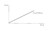
- the relationship is as shown in the graph of FIG.
- y) AV becomes an offset B (x, y), the difference between the offset B (x, y) and the maximum value V (x, y) MAX , and the offset B (x, y) and the minimum value V ( x, y)
- the difference from MIN is the gain A (x, y).
- the luminance value V (x, y) changes in proportion to the luminance L or the reflectance R (x, y) of the light source, for example, at the coordinate position where the reflectance R is halved, the gain A and the offset B The value of is also halved.
- the offset B (x, y) increases and decreases and the offset B (x, y)
- the gain A (x, y) also increases / decreases in proportion to. If one of the gain A and the offset B is known from the equation (F8), the other can be obtained.
- the proportionality constant K is determined by the transmittance G of the grating irrespective of the luminance L and the reflectance R of the light source. That is, the following means 2 and 3 can be used in other words.
- the luminance L of the light source is changed (for example, when the first luminance is changed to the second luminance)
- the luminance value V (x, y) of the measured coordinates (x, y) on the image data and thus While the gain A (x, y) and the offset B (x, y) of the light pattern relating to the measured coordinates (x, y) are different from each other, the proportionality constant K is set to the luminance L of the light source. Does not change, so it does not change. That is, the values of the gain A and the offset B are different between the first light pattern and the second light pattern irradiated using the same grating, but the proportionality constant K is not changed at all.
- the structure which irradiates simultaneously to the to-be-measured object the several light pattern from which a phase differs in each wavelength (RGB component)
- three types of image data from which a phase differs will be acquired by one imaging. It is possible.
- the light pattern of each RGB component light pattern, the brightness of the light source, the reflectance at the object to be measured, the transmittance of the grating, the conversion efficiency of the image sensor, and the like are different.
- the values of the gain A and the offset B relating to are also different.
- the values of the gain A and the offset B related to the light patterns of the RGB components are the same. Assuming that the calculation is performed ignoring the error, the measurement accuracy may be significantly reduced.
- this means 1 when acquiring a plurality of types of image data having different phases, there is no difference in the values of the gain A and the offset B between the respective image data, so that the reduction in measurement accuracy is suppressed. be able to.
- the relationship between the gain A and the offset B is uniquely determined, for example, by creating a numerical table or table data representing the relationship between the gain A and the offset B, the offset B from the gain A or the offset
- the gain A can be obtained from B.
- Means 3 The three-dimensional measuring apparatus according to claim 1, wherein the gain and the offset are proportional to each other.
- Means 4 When the luminance value of each pixel of the two types of image data when the relative phase relationship of the second light pattern having the two phase changes is set to 0 and ⁇ , respectively, is V 0 and V 1 , The second measuring means performs measurement related to the second measurement target region.
- the three-dimensional measuring apparatus according to any one of means 1 to 3, wherein a phase ⁇ satisfying a relationship of the following formulas (1), (2), and (3) is calculated.
- V 0 Asin ⁇ + B (1)
- V 1 Asin ( ⁇ + ⁇ ) + B (2)
- A KB (3)
- calculating phase ⁇ satisfying the relationship of the following formulas (1), (2), (3)” in the above means 4 means “calculating the phase ⁇ based on the following formula (9).
- the algorithm for obtaining the phase ⁇ is not limited to the above equation (9), and any other configuration may be adopted as long as the relationship of the above equations (1), (2), and (3) is satisfied. May be.
- the imaging is performed twice under the two second light patterns whose phases are different by 180 °.
- the following formula (11) can be derived from the above formulas (1) and (10).
- the following formula (12) can be derived.
- phase ⁇ sin ⁇ 1 [(V 0 ⁇ V 1 ) / K (V 0 + V 1 )] (15) That is, the phase ⁇ can be specified by the known luminance values V 0 and V 1 and the constant K.
- the phase ⁇ can be obtained based on a relatively simple arithmetic expression, and it is possible to further speed up the processing when performing the three-dimensional measurement of the measurement object.
- the imaging is performed twice under the two second light patterns whose phases are different by 90 °.
- the offset B can be specified by the known luminance values V 0 and V 1 and the constant K.
- phase ⁇ tan ⁇ 1 ⁇ (V 0 ⁇ B) / (V 1 ⁇ B) ⁇ (27) That is, the phase ⁇ can be specified by the known luminance values V 0 and V 1 and the constant K by using the above equation (23).
- the phase ⁇ can be obtained based on the arithmetic expression using “tan ⁇ 1 ”, so that the height can be measured in the range of 360 ° from ⁇ 180 ° to 180 °.
- the measurement range can be made larger.
- Means 7 One of said 1st measurement object area
- the measurement related area can be measured more appropriately with the measurement reference area as the reference plane, and the measurement accuracy can be improved.
- the first measurement target region with a large number of imaging is the “inspection target region”.
- Means 8 The three-dimensional measuring apparatus according to any one of means 1 to 7, wherein the object to be measured is a printed board on which cream solder is printed, or a wafer board on which solder bumps are formed.
- the height of the solder paste printed on the printed circuit board or the solder bump formed on the wafer substrate can be measured.
- the quality of cream solder or solder bumps can be determined based on the measured values. Therefore, in such an inspection, the effect of each means described above is exhibited, and the quality determination can be performed with high accuracy. As a result, it is possible to improve the inspection accuracy in the solder printing inspection apparatus or the solder bump inspection apparatus.
- the “inspection area (for example, the first measurement area)” may be a “solder area” on which cream solder is printed.
- the “measurement reference region (for example, the second measurement target region)” is a “background region” other than the solder region.
- the “background region” is a portion where an electrode pattern not printed with cream solder is exposed, a portion where a base substrate made of glass epoxy resin or the like is exposed, or a portion of a resist film covering the electrode pattern Or a portion of a resist film covering the base substrate.
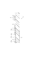
- the printed circuit board 1 is provided with an electrode pattern 3 made of copper foil on a flat base board 2 made of glass epoxy resin or the like. Further, cream solder 4 is printed on the predetermined electrode pattern 3.
- the area where the cream solder 4 is printed is referred to as “solder area”.
- a portion other than the solder region is collectively referred to as a “background region”.
- the background region includes a region where the electrode pattern 3 is exposed (symbol PA), a region where the base substrate 2 is exposed (symbol PB), and the base substrate 2.
- a region where the resist film 5 is coated (symbol PC) and a region where the resist film 5 is coated on the electrode pattern 3 (symbol PD) are included. Note that the resist film 5 is coated on the surface of the printed circuit board 1 so that the cream solder 4 is not applied to portions other than the predetermined wiring portion.
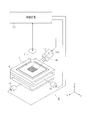
- FIG. 1 is a schematic configuration diagram schematically showing the substrate inspection apparatus 8.
- the substrate inspection apparatus 8 includes a mounting table 9 for mounting the printed circuit board 1 and an illuminating device as an irradiating unit that irradiates a predetermined light pattern on the surface of the printed circuit board 1 obliquely from above. 10, a camera 11 as an imaging unit for imaging a portion irradiated with the light pattern on the printed circuit board 1, and a control device for performing various controls, image processing, and arithmetic processing in the substrate inspection apparatus 8. 12.
- the mounting table 9 is provided with motors 15 and 16.
- the motors 15 and 16 are driven and controlled by the control device 12, the printed circuit board 1 mounted on the mounting table 9 can move in any direction ( X-axis direction and Y-axis direction).
- the illumination device 10 includes a light source 10a and a liquid crystal lattice 10b that converts light from the light source 10a into a light pattern having a sinusoidal (stripe) light intensity distribution.
- a sinusoidal (stripe) light intensity distribution it is possible to irradiate a striped light pattern whose phase changes in multiple ways.
- the illumination device 10 light emitted from the light source 10a is guided to a pair of condensing lenses by an optical fiber, and is converted into parallel light there.
- the parallel light is guided to the projection lens through the liquid crystal grating 10b. Then, a striped light pattern is irradiated onto the printed circuit board 1 from the projection lens.
- the illumination device 10 is configured to be able to change the luminance of light emitted from the light source 10a.
- the luminance setting process described later it is possible to switch between at least the luminance for solder corresponding to the solder area and the luminance for background corresponding to the background area.
- soldering luminance corresponds to “first luminance” in the present embodiment
- background luminance corresponds to “second luminance” in the present embodiment.
- the liquid crystal lattice 10b has a liquid crystal layer formed between a pair of transparent substrates, a common electrode disposed on one transparent substrate, and a plurality of strips arranged in parallel on the other transparent substrate so as to face the common electrode.
- Each of the grids corresponding to each band electrode by controlling on and off the switching elements (thin film transistors, etc.) connected to each band electrode by a drive circuit and controlling the voltage applied to each band electrode.
- the light transmittance of the line is switched to form a striped lattice pattern composed of a “bright portion” having a high light transmittance and a “dark portion” having a low light transmittance.
- the light irradiated on the printed circuit board 1 via the liquid crystal grating 10b becomes a light pattern having a sinusoidal light intensity distribution due to blur caused by diffraction action or the like.
- the camera 11 includes a lens, an image sensor, and the like.
- a CMOS sensor is used as the image sensor.
- the imaging device is not limited to this, and a CCD sensor or the like may be employed, for example.
- Image data captured by the camera 11 is converted into a digital signal inside the camera 11, input to the control device 12 in the form of a digital signal, and stored in a data storage device 24 described later. Then, the control device 12 performs image processing, inspection processing, and the like, which will be described later, based on the image data. In this sense, the control device 12 constitutes image processing means.
- the control device 12 includes a CPU and input / output interface 21 (hereinafter referred to as “CPU etc. 21”) that controls the board inspection device 8 as a whole, and a keyboard, a mouse, or a touch panel.
- CPU etc. 21 a CPU and input / output interface 21
- the input device 22 as the “input means”
- the display device 23 as the “display means” having a display screen such as a CRT or a liquid crystal
- image data captured by the camera 11 and various calculation data are examples of the image data captured by the camera 11 and various calculation data.
- These devices 22 to 27 are electrically connected to the CPU 21 or the like.
- the database 27 includes a solder table 27A indicating the correspondence between the solder area (type of cream solder 4) and the luminance of the illumination device 10 corresponding to the solder area, and the background area (type of printed circuit board 1) and the illumination apparatus corresponding thereto.
- the board table 27B indicating the correspondence with the luminance of 10 is stored.
- the solder table 27A is manufactured by the manufacturer of the cream solder 4 printed in the solder area such as the company a, the company b, and the company c and the illumination corresponding thereto.
- the correspondence relationship with the brightness of the device 10 is shown.
- the board table 27B shows a correspondence relationship between the colors of the background regions such as green, blue, and black and the luminance of the illumination device 10 according to them. Yes.
- This brightness setting process is repeatedly executed by selecting and operating the “set” button displayed on the display screen of the display device 23.
- the selection operation of the “setting” button is performed via the input device 22.
- the selection operation is performed with a pointing device such as a mouse, or the selection operation is performed with a touch panel integrated with the display device 23. As realized.
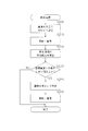
- steps are simply indicated by symbol S 100, it is determined whether or not the type of the printed circuit board 1 to be inspected has been input.
- the printed circuit board 1 is assumed to have an inspection area or the like set for each type specified here. If it is determined that a product type has been input (S100: YES), product type information is displayed in S110, and the process proceeds to S120. On the other hand, when it is determined that the product type has not been input (S100: NO), the following process is not executed and the brightness setting process is temporarily terminated.
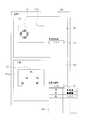
- FIG. 1 A display example of product type information in S110 is shown in FIG. Here, for example, the case where “type J” is selected is shown. Specifically, a window W1 is displayed. This window W1 is composed of windows W2 and W3. The window W2 displays solder area information, and the window W3 displays background area information. The entire images PG1, PG2 of the printed circuit board 1 are displayed in both windows W2, W3. The whole images PG1 and PG2 are prepared in advance. Of course, you may make it acquire whole image PG1, PG2 based on the imaging by the camera 11. FIG.
- the solder image PG1 displayed in the window W2 is a solder area on which the cream solder 4 is printed, and an inspection target area 31 (an area shown by hatching in the window W2) to be inspected. It is displayed.
- the “inspection area 31” corresponds to the “first measurement area” in the present embodiment.
- the background image PG2 displayed in the window W3 is a part of the background area and is a reference area for measurement such as height measurement (an area shown by hatching in the window W3). Is displayed.
- the “measurement reference region 32” corresponds to the “second measurement target region” in the present embodiment.
- a solder luminance input field 33 is displayed in the window W2
- a background luminance input field 34 is displayed in the window W3.
- the luminance values may be displayed by default, or in the stage of S110, the input fields 33 and 34 may be displayed blank.
- solder luminance input field 33 it is determined whether or not the solder luminance input field 33 is selected.
- the selection of the solder luminance input field 33 is performed by a selection operation via the input device 22. That is, similarly to the above-described “setting” button selection operation, for example, a selection operation may be performed using a pointing device such as a mouse, or a selection operation may be performed using a touch panel integrated with the display device 23. The same applies to the selection operation on the display screen. If it is determined that the input field 33 is selected (S120: YES), a selection list (which will be described later) is displayed in S130, and the process proceeds to S140. On the other hand, when it is determined that the input field 33 is not selected (S120: NO), the process proceeds to S160.
- S140 it is determined whether a luminance value is selected from the selection list. If it is determined that the luminance value has been selected (S140: YES), the setting process of the luminance for solder is performed in S150, and the process proceeds to S160. On the other hand, this determination process is repeated until the luminance value is not selected (S140: NO). Of course, if no selection is made even after a predetermined time has elapsed, the processing may be terminated, or a warning or the like may be given (the same applies to S180).
- S160 it is determined whether or not the background luminance input field 34 has been selected.
- the selection of the background luminance input field 34 is performed by a selection operation via the input device 22. If it is determined that the input field 34 has been selected (S160: YES), a selection list (to be described later) is displayed in S170, and the process proceeds to S180. On the other hand, when it is determined that the input field 34 is not selected (S160: NO), the process proceeds to S200.
- S180 it is determined whether a luminance value is selected from the selection list. If it is determined that a luminance value has been selected (S180: YES), background luminance setting processing is performed in S190, and the process proceeds to S200. On the other hand, this determination process is repeated until the luminance value is not selected (S180: NO).
- S200 it is determined whether or not there is an end instruction. This end instruction is given by selecting an “end” button on a screen (not shown). If it is determined that an end instruction has been given (S200: YES), the brightness setting process is ended. On the other hand, if it is determined that there is no termination instruction (S200: NO), the processing from S120 is repeated.
- the display of the selection list in S170 is performed, for example, in the form shown in FIG. That is, when the background luminance input field 34 is selected (S160: YES), a new window W4 is displayed below the input field 34.
- the content of the displayed selection list is the correspondence between the color and the brightness in the substrate table shown in FIG.
- a luminance value shown by a black triangle or the like in the figure
- the luminance value is set (S190), and the background luminance input field 34 is set. Is displayed.
- the luminance value is selected.
- the substrate type (color) indicated as “green”, “blue”, “black”, or the like may be selected, or these luminance values may be selected. Alternatively, either one of the substrate types may be selected.
- This inspection routine is executed by the control device 12 (CPU 21 or the like).
- the control device 12 first drives and controls the motors 15 and 16 to move the printed circuit board 1 and adjusts the field of view of the camera 11 to a predetermined inspection area (measurement range) on the printed circuit board 1.
- the inspection area is one area in which the surface of the printed circuit board 1 is divided in advance with the size of the field of view of the camera 11 as one unit.
- the control device 12 performs a setting process for the lighting device 10. More specifically, the luminance switching control process of the light source 10a and the liquid crystal lattice 10b switching control process are performed. Specifically, the luminance of the light emitted from the light source 10a is switched to the luminance for solder (first luminance) determined in advance by the luminance setting process, and the liquid crystal lattice 10b is switched and controlled. The position of the grating formed in 10b is set to a predetermined reference position (phase “0 °”).
- the “brightness control unit” in the present embodiment is configured by the function of performing the luminance switching control process of the light source 10a by the control device 12, and the “phase control unit” is configured by the function of performing the switching control process of the liquid crystal grating 10b.
- the control device 12 causes the light source 10a of the illumination device 10 to emit light, starts the irradiation of the first light pattern with the luminance for soldering, and the phase of the first light pattern. Are sequentially shifted by 90 ° into four phases (phase “0 °”, phase “90 °”, phase “180 °”, phase “270 °”).
- the control device 12 drives and controls the camera 11 each time the phase of the first light pattern is sequentially shifted, and images the inspection area portion irradiated with the first light pattern. Accordingly, four types of image data captured under the first light pattern with the phase shifted by 90 ° with respect to the predetermined inspection area are acquired. Here, the image data captured by the camera 11 is transferred to and stored in the data storage device 24.
- control device 12 calculates the phase ⁇ 1 of the first light pattern related to each pixel from the above four image data (luminance values) by the phase shift method.
- the luminance values V 10 , V 11 , V 12 , and V 13 relating to the respective pixels of the four types of image data are represented by the following formulas (H1), (H2), (H3), and (H4). it can.
- the first measuring means in this embodiment is constituted by these series of processing functions.
- the relationship grasping means in this embodiment is constituted by such processing functions.
- the process of grasping the relationship between the gain A 1 and the offset B 1 is performed in parallel with the above-described calculation process of the height data related to the inspection target region 31 after the acquisition of the four types of image data (after imaging). Is called.
- proportionality constant K of the gain A 1 and the offset B 1 is calculated based on the following formula (H11) derived from the above formulas (H6) and (H10).
- the proportional constant K of the gain A 1 and the offset B 1 relating to each pixel calculated in this way is stored in the data storage device 24.
- the control device 12 starts an imaging process related to the measurement reference region 32.
- the imaging processing related to the measurement reference region 32 is started immediately after the series of imaging processing related to the inspection target region 31 is completed. That is, it is performed in parallel with the above-described calculation process of the height data related to the inspection target region 31 and the calculation process of the proportionality constant K of the gain A 1 and the offset B 1 .
- the luminance switching control process of the light source 10a and the switching control process of the liquid crystal lattice 10b are performed. Specifically, the luminance of the light emitted from the light source 10a is switched to the background luminance (second luminance) determined in advance by the luminance setting process, and the liquid crystal lattice 10b is switched and controlled. The position of the grating formed in 10b is set to a predetermined reference position (phase “0 °”).
- the control device 12 causes the light source 10a of the illumination device 10 to emit light, starts irradiating the second light pattern with the background luminance, and the phase of the second light pattern. Are sequentially shifted into two phases (phase “0 °”, phase “180 °”).
- the control device 12 drives and controls the camera 11 every time the phase of the second light pattern is sequentially shifted, and images the inspection area portion irradiated with the second light pattern. Thereby, two types of image data captured under the second light pattern whose phase is shifted by 180 ° with respect to the predetermined inspection area are acquired.
- the image data captured by the camera 11 is transferred to and stored in the data storage device 24.
- control device 12 calculates the phase ⁇ 2 of the second light pattern relating to each pixel of the measurement reference region 32 by the phase shift method based on the two types of image data.
- phase ⁇ 2 of the second light pattern is expressed by the following equation (15) based on the above equation (15) when the luminance values relating to the respective pixels of the two types of image data are V 20 and V 21 , respectively. 15 ′).
- the proportional constant K A 2 / B 2
- the proportional constant K A 1 / B 1
- the control device 12 calculates the height and volume of the cream solder 4 in the inspection target region 31, the printing range, and the like using the measurement reference region 32 as a height reference plane. Then, the control device 12 compares the data such as the position, area, height, or volume of the cream solder 4 thus determined with reference data stored in advance, and whether the comparison result is within an allowable range. Whether or not the printing state of the cream solder 4 in the inspection area is good or bad is determined based on whether or not it is. The inspection result is stored in the inspection result storage device 26.
- control device 12 drives and controls the motors 15 and 16 to move the printed circuit board 1 to the next inspection area. Thereafter, the above series of processing is performed in all inspection areas. The inspection of the entire printed circuit board 1 is completed by being repeatedly performed.
- the three-dimensional measurement related to the inspection target region 31 is performed based on the image data captured by irradiating the first light pattern having the first luminance corresponding to the inspection target region 31.
- the three-dimensional measurement related to the measurement reference region 32 is performed based on the image data captured by irradiating the second light pattern having the second luminance corresponding to the measurement reference region 32.
- the relationship between the gain A and the offset B (proportional constant K) of the light pattern determined by a predetermined imaging condition is grasped from four types of image data captured for the purpose of measuring the inspection target region 31.
- the gain A or the offset B value of the light pattern related to the pixel is used.
- three-dimensional measurement can be performed by the phase shift method based on two types of image data captured under a light pattern whose phase has been changed in two ways.
- the first light pattern having the first luminance is irradiated with the four phases, the four images are captured under the first light pattern, and then the second light pattern having the second luminance is formed in the two ways. Since it is only necessary to irradiate with the phase and take two images under the phase, the number of times of imaging is six times, and the imaging time is greatly reduced.
- the total number of times of imaging can be reduced, and the imaging time can be shortened. As a result, the measurement time can be dramatically shortened.
- the measurement reference region 32 is configured to perform three-dimensional measurement based on two types of image data having a phase difference of 180 °, so that the measurement range is 180 from ⁇ 90 ° to 90 °.
- the measurement reference region 32 serving as a reference surface is flat and has a substantially uniform height, so that there is no particular problem even if the measurement range is narrow.
- the brightness corresponding to the case where the substrate type (substrate color) is “black” is also prepared in the substrate table 27B of FIG.
- the measurement reference region 32 background region
- the difference in lightness and darkness in the measurement reference region 32 This is because there is a high possibility that the (luminance difference) will be small. Therefore, according to the present embodiment, when the measurement reference area 32 is black or gray that is relatively close to black, the effect is conspicuous.
- the present embodiment it is determined whether or not three-dimensional measurement of the measurement reference region 32 is possible based on image data obtained by irradiating a light pattern with a first luminance corresponding to the inspection target region 31 and picking up the image.
- the first luminance is corrected to the second luminance corresponding to the measurement reference region 32, and the light pattern is irradiated with the second luminance.
- the luminance of the lighting device 10 is set in accordance with the cream solder 4. This luminance is predetermined as the luminance for solder (first luminance).
- the lighting device 10 is turned on by the control device 12 so as to achieve the set soldering luminance, and the surface of the printed circuit board 1 is irradiated with the first light pattern having the first luminance obliquely from above.
- the control device 12 drives and controls the camera 11 each time the phase of the first light pattern is sequentially shifted, and images the inspection area portion irradiated with the first light pattern. As a result, four types of image data captured under the first light pattern whose phase is shifted by 90 ° are acquired.
- the average luminance of the background region is calculated based on the image data captured in S210.
- subsequent S230 it is determined whether the difference between the target luminance of the background area and the average luminance calculated in S220 is equal to or greater than a threshold value. If it is determined that the difference is greater than or equal to the threshold value (S230: YES), the process proceeds to S240. On the other hand, when the difference is below the threshold value (S230: NO), the subsequent processing is not executed and the present imaging processing is terminated.
- step S240 where the difference is determined to be greater than or equal to the threshold value, the luminance is corrected. Specifically, the luminance of the lighting device 10 is corrected and set based on the ratio between the average luminance and the target luminance calculated in S220. That is, the luminance for solder (first luminance) is corrected and the luminance for background (second luminance) is set.
- the lighting device 10 is turned on by the control device 12 so as to obtain the corrected background luminance, and the surface of the printed circuit board 1 is irradiated with the second light pattern having the second luminance from obliquely above.
- the control device 12 drives and controls the camera 11 every time the phase of the second light pattern is sequentially shifted, and images the inspection area portion irradiated with the second light pattern. Thereby, two kinds of image data captured under the second light pattern whose phase is shifted by 180 ° are acquired.
- FIG. 9 schematically shows the luminance of the light pattern in the background area as a graph.
- the ideal luminance for performing the three-dimensional measurement of the background region is indicated by a two-dot chain line at the top of the graph.
- a sine curve having a certain amplitude is desirable.
- a sine curve having a small amplitude as indicated by a solid line at the bottom of the graph may occur when the background area is a relatively dark color. is there. That is, the difference in brightness (brightness difference) becomes small.
- the average luminance of the background area is calculated (S220 in FIG. 8), and it is determined whether or not the difference from the target luminance is equal to or larger than the threshold (S230). If this is the case (S230: YES), the luminance for solder is corrected and the luminance for background is set (S240).
- the average value of the luminance of the background region that is, the average value N of the sine curve at the bottom of the graph is calculated (S220), and the difference D from the target value M, which is a predetermined ideal average value of luminance. Is greater than or equal to a threshold value (S230).
- the background brightness is set by correcting the solder brightness based on the ratio between the target value M and the average value N. Specifically, the luminance for solder is set to (M / N) times to set the luminance for background.
- control device 12 performs three-dimensional measurement of the inspection target region 31 and the measurement reference region 32 based on image data obtained by irradiation with solder luminance. .
- the height and volume of the cream solder 4 in the inspection target region 31 are measured using the measurement reference region 32 as a height reference plane.
- the illuminating device 10 is turned on with the soldering brightness determined in advance in accordance with the solder area (inspection area 31) under the premise that the color of the cream solder 4 is not so different depending on the manufacturer. Imaging is performed (S200 and S210 in FIG. 8). And based on the image data imaged under the 1st light pattern of this brightness
- the average value of the luminance of the background region is calculated (S220), and when the difference from the luminance target value is equal to or larger than the threshold value ( (S230: YES), the luminance for solder is corrected using the ratio with the target value, and the luminance for background is set (S240).
- the lighting device 10 is turned on with the background luminance and imaging is performed (S250).
- region 32 can be performed.
- the measurement reference region 32 (background region) is black or gray that is relatively close to black
- the difference in brightness in the background region There is a high possibility that (luminance difference) will be reduced.
- the three-dimensional measurement of the measurement reference region 32 can be performed by correcting the ratio between the average value of the actual luminance and the target value, the measurement reference region 32 is black or relatively close to black. If it is gray, the effect is noticeable.
- the three-dimensional measuring device is embodied as the substrate inspection device 8 that measures the height of the cream solder 4 printed on the printed circuit board 1. It may be embodied in a configuration for measuring the height of other things such as solder bumps printed on the board or electronic parts mounted on the substrate. For example, in the case of a wafer substrate, the surface of the oxide film can be used as the reference height, and the height, shape, volume, etc. of the solder bumps can be calculated.
- the grating for converting the light from the light source 10a into a striped light pattern is constituted by the liquid crystal grating 10b, and the phase of the light pattern is shifted by switching this. It has a configuration.
- the grating member may be transferred by a transfer unit such as a piezo actuator to shift the phase of the light pattern.
- the present invention is not limited to this.
- the three types are captured under three first light patterns whose phases are different by 120 °. It is good also as a structure which performs three-dimensional measurement based on this image data. That is, the “predetermined number” that is the number of times of imaging of the first measurement target region under the first light pattern may be a number that can perform at least three-dimensional measurement by the phase shift method.
- two types of image data captured under two types of light patterns that are 180 degrees out of phase when measuring the second measurement target region (measurement reference region 32) using the second light pattern. Based on this, it is configured to perform three-dimensional measurement.
- a configuration may be used in which three-dimensional measurement is performed based on two types of image data captured under two types of light patterns whose phases are different by 90 °.
- the luminance values V 20 and V 21 at each pixel on the two types of image data and the known proportionality constant K are used to obtain the first value at each pixel.
- the phase ⁇ 2 of the two light pattern can be calculated.
- the phase ⁇ 2 can be obtained based on an arithmetic expression using “tan ⁇ 1 ”, the height can be measured in the range of 360 ° from ⁇ 180 ° to 180 °, and the measurement range is increased. Can be larger.
- the relationship between the gain A and the offset B is not obtained as an expression, but a numerical table or table data representing the relationship between the gain A and the offset B is created, so that the gain A is offset B or the offset B is gain A. It may be possible to obtain
- solder table 27A having different brightness is stored for each manufacturer. However, the color of the solder area (area where the cream solder 4 is printed) is relatively stable. If there is, the solder table 27A may be omitted. In other words, as in the second embodiment, focusing on the fact that there is no significant difference among manufacturers, a configuration in which the illumination device 10 is turned on with a predetermined luminance when imaging for the purpose of measuring the inspection target region 31 is performed. It is good.
- the same background luminance is set for a plurality of measurement reference regions 32 (background regions), and imaging is performed based on irradiation of the illumination device 10 with the background luminance.
- a plurality of measurement reference regions 32 may be imaged by irradiation with different luminances. This is because the plurality of measurement reference regions 32 are not necessarily the same color. Therefore, as shown in FIG. 10, in the display of product type information, symbols such as U1 to U5 are displayed corresponding to each measurement reference region 32, and the background luminance can be set for each measurement reference region 32. Also good.
- the input field 35 is prepared so as to correspond to the symbol displayed on the image PG2 of the printed circuit board 1.
- the luminance for solder is corrected by the ratio between the average value of the luminance of the background area in the image data and the target value.
- the soldering luminance is corrected with a relatively simple calculation formula, but the luminance and the luminance of the image data are not completely linearly proportional.
- correction information may be stored in the database 27 in advance.
- the correction information may be a correction magnification of the luminance for solder according to the average value of the luminance of the background area. Then, when it is determined that the three-dimensional measurement of the measurement reference region 32 is impossible based on the imaging with the first light pattern, the luminance for solder is corrected with reference to this correction information to set the luminance for background. In this way, the background luminance to be set becomes more appropriate, and the three-dimensional measurement of the measurement reference region 32 can be reliably executed by imaging with the background luminance.
- the effect is conspicuous when the measurement reference region 32 (background region) is black or gray that is relatively close to black.
- the measurement reference region 32 (background region) is white or relative.
- the luminance in the measurement reference region 32 (background region) becomes too high in the image data captured with the luminance corresponding to the inspection target region 31 (solder region).
- the effect is conspicuous even when the measurement reference region 32 (background region) is white or gray that is relatively close to white.
- SYMBOLS 1 Printed circuit board, 2 ... Base substrate, 3 ... Electrode pattern, 4 ... Cream solder, 5 ... Resist film, 8 ... Board inspection apparatus, 10 ... Illumination device, 10a ... Light source, 10b ... Liquid crystal lattice, 11 ... Camera, 12 DESCRIPTION OF SYMBOLS ... Control device, 24 ... Data storage device, 25 ... Three-dimensional arithmetic unit, 26 ... Inspection result storage device, 27 ... Database, 27A ... Solder table, 27B ... Substrate table, 31 ... Inspection object area, 32 ... Measurement standard Area, A 1 , A 2 ... gain, B 1 , B 2 ... offset, K ... proportional constant.
Landscapes
- Engineering & Computer Science (AREA)
- Physics & Mathematics (AREA)
- General Physics & Mathematics (AREA)
- Computer Vision & Pattern Recognition (AREA)
- Theoretical Computer Science (AREA)
- Optics & Photonics (AREA)
- Operations Research (AREA)
- Manufacturing & Machinery (AREA)
- Immunology (AREA)
- Pathology (AREA)
- Microelectronics & Electronic Packaging (AREA)
- Biochemistry (AREA)
- Analytical Chemistry (AREA)
- Chemical & Material Sciences (AREA)
- Life Sciences & Earth Sciences (AREA)
- Health & Medical Sciences (AREA)
- General Health & Medical Sciences (AREA)
- Geometry (AREA)
- Quality & Reliability (AREA)
- Length Measuring Devices By Optical Means (AREA)
- Image Processing (AREA)
- Image Analysis (AREA)
Abstract
位相シフト法を利用した三次元計測を行うにあたり、より高精度な計測をより短時間で実現することのできる三次元計測装置を提供する。基板検査装置8は、プリント基板1に対し所定の光パターンを照射する照明装置10と、その光パターンの照射された部分を撮像するカメラ11と、各種制御や画像処理、演算処理を実施する制御装置12とを備えている。制御装置12は、まず半田領域に応じた第1輝度の第1光パターンを4通りの位相で照射し撮像された4通りの画像データを基に、半田領域に係る三次元計測を行うと共に、該4通りの画像データを基に所定の撮像条件により定まるゲイン及びオフセットの関係を把握する。次に背景領域に応じた第2輝度の第2光パターンを2通りの位相で照射し撮像された2通りの画像データを基に、前記ゲイン及びオフセットの関係を利用して、背景領域に係る三次元計測を行う。
Description
本発明は、位相シフト法を利用して三次元計測を行う三次元計測装置に関するものである。
一般に、プリント基板は、ガラスエポキシ樹脂からなるベース基板の上に電極パターンを具備し、表面がレジスト膜によって保護されている。かかるプリント基板上に電子部品を実装する場合、まず電極パターン上のレジスト膜による保護がされていない所定位置にクリーム半田が印刷される。次に、該クリーム半田の粘性に基づいてプリント基板上に電子部品が仮止めされる。その後、前記プリント基板がリフロー炉へ導かれ、所定のリフロー工程を経ることで半田付けが行われる。昨今では、リフロー炉に導かれる前段階においてクリーム半田の印刷状態を検査する必要があり、かかる検査に際して三次元計測装置が用いられることがある。
該位相シフト法を利用した三次元計測装置においては、所定の光を発する光源と、該光源からの光を正弦波状(縞状)の光強度分布を有する光パターンに変換する格子との組み合わせからなる照射手段により、光パターンを被計測物(この場合、プリント基板)に照射する。そして、基板上の点を真上に配置した撮像手段を用いて観測する。撮像手段としては、レンズ及び撮像素子等からなるCCDカメラ等が用いられる。
上記構成の下、撮像手段により撮像された画像データ上の各座標(画素)の光の強度(輝度)Iは下式(T1)で与えられる。
I=f・sinφ+e ・・(T1)
但し、f:ゲイン、e:オフセット、φ:光パターンの位相。
但し、f:ゲイン、e:オフセット、φ:光パターンの位相。
ここで、上記格子を切換制御することにより、光パターンの位相を例えば4段階(φ+0、φ+90°、φ+180°、φ+270°)に変化させ、これらに対応する強度分布I0、I1、I2、I3をもつ画像データを取り込み、下記式(T2)に基づいてf(ゲイン)とe(オフセット)をキャンセルし、位相φを求める。
φ=tan-1[(I1-I3)/(I2-I0)] ・・(T2)
そして、この位相φを用いて、三角測量の原理に基づき被計測物上の各座標(X,Y)における高さ(Z)が求められる。
そして、この位相φを用いて、三角測量の原理に基づき被計測物上の各座標(X,Y)における高さ(Z)が求められる。
ところが、プリント基板上のクリーム半田の印刷部分の周囲(以下、背景領域という)の色は様々である。これは、ガラスエポキシ樹脂やレジスト膜に種々の色が使用されるためである。そして、例えば黒色などの比較的暗い色の背景領域では、撮像手段により撮像された画像データのコントラストが小さくなってしまう。つまり、画像データ上、上記光パターンの明暗の差(輝度差)が小さくなってしまうのである。そのため、背景領域の高さ計測が困難となるおそれがある。本来であれば基板上に印刷されたクリーム半田の高さをより高精度で計測するためには、その基板内に高さ基準を採ることが望ましい。しかしながら、背景領域を高さ基準面として適正に利用できないため、その基板内に高さ基準を採ることができないといった不具合を生じるおそれがある。
これに鑑み、近年では、輝度が異なる2種類の光パターンを利用して計測を行う三次元計測装置も提案されている(例えば、特許文献1参照)。具体的には、第1の輝度の光パターンを照射して得られた画像データに基づき、プリント基板上の検査対象領域(半田領域)に係る三次元計測を行うと共に、第2の輝度の光パターンを照射して得られた画像データに基づき、プリント基板上の計測基準領域(背景領域)に係る三次元計測を行い、計測基準領域を高さ基準面として検査対象領域のクリーム半田の高さや体積が計測されることとなる。
しかしながら、上記のとおり、位相シフト法を利用した従来の三次元計測装置においては、照射する光パターンの位相を4段階(又は3段階)に変化させ、4通り(又は3通り)の画像を撮像する必要がある。
従って、輝度の異なる2種類の光パターンを切換えて計測を行う場合には、まず第1輝度の第1光パターンを照射し、その位相を4段階(又は3段階)に変化させ、これらの下で4通り(又は3通り)の画像を撮像した後、輝度を変えて、第2輝度の第2光パターンを照射し、その位相を4段階(又は3段階)に変化させ、これらの下で4通り(又は3通り)の画像を撮像するといったように、各輝度の光パターンの下でそれぞれ4回(又は3回)ずつ、計8回(又は6回)の撮像が必要となり、撮像時間が大幅に増大するおそれがあった。
また、一枚のプリント基板上に計測対象範囲が多数設定されているような場合には、該一枚のプリント基板の計測に要する時間はさらにその数倍となる。そのため、計測時間のさらなる短縮化が求められる。
尚、上記課題は、必ずしもプリント基板上に印刷されたクリーム半田等の高さ計測に限らず、他の三次元計測装置の分野においても内在するものである。
本発明は、上記事情に鑑みてなされたものであり、その目的は、位相シフト法を利用した三次元計測を行うにあたり、より高精度な計測をより短時間で実現することのできる三次元計測装置を提供することにある。
以下、上記課題を解決するのに適した各手段につき項分けして説明する。なお、必要に応じて対応する手段に特有の作用効果を付記する。
手段1.所定の光を発する光源、及び、該光源からの光を縞状の光強度分布を有する光パターンに変換する格子を有し、該光パターンを少なくとも第1計測対象領域及び第2計測対象領域を有する被計測物に対し照射可能な照射手段と、
前記光源から発せられる光の輝度を変更可能な輝度制御手段と、
前記格子の移送又は切替を制御し、前記照射手段から照射する前記光パターンの位相を複数通りに変化可能な位相制御手段と、
前記光パターンの照射された前記被計測物からの反射光を撮像可能な撮像手段と、
前記撮像手段により撮像された画像データを基に位相シフト法により前記被計測物の三次元計測を実行可能な画像処理手段とを備え、
前記画像処理手段は、
前記第1計測対象領域に応じた第1輝度の第1光パターンを所定数通り(例えば3通り又は4通り)の位相で照射し撮像された所定数通りの画像データを基に、前記第1計測対象領域に係る三次元計測を行う第1計測手段と、
前記第1光パターンの下で撮像された前記所定数通りの画像データを基に、所定の撮像条件により定まるゲイン及びオフセットの関係を把握する関係把握手段と、
前記第2計測対象領域に応じた第2輝度の第2光パターンを2通りの位相で照射し撮像された2通りの画像データを基に、該2通りの画像データの各画素の輝度値から定まる該画素に係るゲイン又はオフセットの値と、前記関係把握手段により把握されたゲイン及びオフセットの関係とを利用して、前記第2計測対象領域に係る三次元計測を行う第2計測手段とを備えたことを特徴とする三次元計測装置。
前記光源から発せられる光の輝度を変更可能な輝度制御手段と、
前記格子の移送又は切替を制御し、前記照射手段から照射する前記光パターンの位相を複数通りに変化可能な位相制御手段と、
前記光パターンの照射された前記被計測物からの反射光を撮像可能な撮像手段と、
前記撮像手段により撮像された画像データを基に位相シフト法により前記被計測物の三次元計測を実行可能な画像処理手段とを備え、
前記画像処理手段は、
前記第1計測対象領域に応じた第1輝度の第1光パターンを所定数通り(例えば3通り又は4通り)の位相で照射し撮像された所定数通りの画像データを基に、前記第1計測対象領域に係る三次元計測を行う第1計測手段と、
前記第1光パターンの下で撮像された前記所定数通りの画像データを基に、所定の撮像条件により定まるゲイン及びオフセットの関係を把握する関係把握手段と、
前記第2計測対象領域に応じた第2輝度の第2光パターンを2通りの位相で照射し撮像された2通りの画像データを基に、該2通りの画像データの各画素の輝度値から定まる該画素に係るゲイン又はオフセットの値と、前記関係把握手段により把握されたゲイン及びオフセットの関係とを利用して、前記第2計測対象領域に係る三次元計測を行う第2計測手段とを備えたことを特徴とする三次元計測装置。
ここで「第1計測対象領域に応じた第1輝度」及び「第2計測対象領域に応じた第2輝度」は、前もって設定しておいても良いし、都度別途計測して求めても良い。また「第1計測対象領域に応じた第1輝度」が既知であれば、「第1計測対象領域に応じた第1輝度」を前もって設定しておき、「第1計測対象領域に応じた第1輝度」による画像データを基に「第2計測対象領域に応じた第2輝度」を求めても良い。
上述したとおり、従来では、第1計測対象領域(例えば半田領域など)の計測を目的として撮像を行った場合、その画像データ上における第2計測対象領域(例えば背景領域など)に関しては、輝度が高すぎたり低すぎたり或いは明暗の差(輝度差)が小さくなってしまうことがある。このような場合、第2計測対象領域に係る計測精度が著しく低下するおそれがある。
この点、上記手段1によれば、第1計測対象領域(例えば比較的明るい明部)に応じた第1輝度の第1光パターンを照射し撮像された画像データを基に該第1計測対象領域に係る三次元計測を行うと共に、第2計測対象領域(例えば比較的暗い暗部)に応じた第2輝度の第2光パターンを照射し撮像された画像データを基に該第2計測対象領域に係る三次元計測を行う構成となっている。これにより、第1計測対象領域及び第2計測対象領域の両者とも、輝度を変えて、それぞれ適正な輝度の光パターンの下で撮像した画像データに基づき三次元計測を行うことができる。結果として、計測精度の低下抑制を図ることができる。
さらに、本手段では、第1計測対象領域の計測を目的として撮像された所定数通りの画像データから、所定の撮像条件により定まるゲインA及びオフセットBの関係〔例えばA=K(比例定数)×B〕を把握する構成となっている。
所定の撮像条件により定まる光パターンのゲインA及びオフセットBの関係と、画像データ上の被計測座標(x,y)の輝度値V(x,y)から定まる、該被計測座標(x,y)に係る光パターンのゲインA(x,y)又はオフセットB(x,y)の値とを利用することにより、2通りに位相変化させた光パターンの下で撮像した2通りの画像データを基に位相シフト法により被計測座標の三次元計測を行うことができる。
つまり、本手段では、第2計測対象領域に関して、少なくとも2通りに位相変化させた第2光パターンの下で撮像された2通りの画像データを取得しさえすれば、位相シフト法による三次元計測が可能となる。
これにより、例えば第1輝度の第1光パターンを4通り(又は3通り)の位相で照射し、その下で4通り(又は3通り)の画像を撮像した後、第2輝度の第2光パターンを2通りの位相で照射し、その下で2通りの画像を撮像する場合には、撮像回数が計6回(又は計5回)となり、撮像時間が大幅に減少する。
従って、光パターンの輝度を変えて被計測物上の異なる領域をそれぞれ三次元計測するだけの従来技術に比べ、総合的な撮像回数が少なくて済み、撮像時間を短縮することができる。結果として、計測時間を飛躍的に短縮することができる。
尚、光源から照射された光は、まず格子を通過する際に減衰され、次に被計測物にて反射する際に減衰され、最後に撮像手段においてA/D変換(アナログ-デジタル変換)される際に減衰された上で、画像データの各画素の輝度値として取得される。
従って、撮像手段により撮像された画像データの各画素の輝度値は、光源の輝度、光源から照射された光が格子を通過する際の減衰率、光が被計測物にて反射する際の反射率、撮像手段においてA/D変換(アナログ-デジタル変換)される際の変換効率等を掛け合わせることにより表現することができる。
例えば、光源(均一光)の輝度:L
格子の透過率:G=αsinθ+β
α,βは任意の定数。
格子の透過率:G=αsinθ+β
α,βは任意の定数。
被計測物上の座標 (x,y)における反射率:R(x,y)
撮像手段(撮像素子)の各画素の変換効率:E
被計測物上の座標(x,y)に対応する画像上の画素の輝度値:V(x,y)
被計測物上の座標(x,y)における光パターンのゲイン:A(x,y)
被計測物上の座標(x,y)における光パターンのオフセット:B(x,y)
とした場合には、下記式(F1)で表すことができる。
撮像手段(撮像素子)の各画素の変換効率:E
被計測物上の座標(x,y)に対応する画像上の画素の輝度値:V(x,y)
被計測物上の座標(x,y)における光パターンのゲイン:A(x,y)
被計測物上の座標(x,y)における光パターンのオフセット:B(x,y)
とした場合には、下記式(F1)で表すことができる。

ここで、ゲインA(x,y)は、「sinθ=1」の光による輝度値V(x,y)MAXと、「sinθ=-1」の光による輝度値V(x,y)MINとの差から表すことができるので、
例えば、格子がθ=0の時の透過率(=平均透過率):Gθ=0
格子がθ=π/2の時の透過率(=最大透過率):Gθ=π/2
格子がθ=-π/2の時の透過率(=最小透過率):Gθ=-π/2
とした場合には、下記式(F2)で表すことができる。
例えば、格子がθ=0の時の透過率(=平均透過率):Gθ=0
格子がθ=π/2の時の透過率(=最大透過率):Gθ=π/2
格子がθ=-π/2の時の透過率(=最小透過率):Gθ=-π/2
とした場合には、下記式(F2)で表すことができる。

また、オフセットB(x,y)は、「sinθ=0」の光における輝度値V(x,y)であって、「sinθ=1」の光による輝度値V(x,y) MAXと、「sinθ=-1」の光による輝度値V(x,y) MINとの平均値であるので、下記式(F3)で表すことができる。

つまり、輝度値の最大値V(x,y)MAX、最小値V(x,y)MIN、平均値V(x,y)AVはそれぞれ下記式(F4)、(F5)、(F6)で表すことができ、図11のグラフに示すような関係となる。

図11から見てとれるように、所定の座標(x,y)における輝度値の最大値V(x,y)MAXと輝度値の最少値V(x,y)MINの平均値V(x,y)AVがオフセットB(x,y)となり、該オフセットB(x,y)と最大値V(x,y)MAXとの差、及び、該オフセットB(x,y)と最少値V(x,y)MINとの差がそれぞれゲインA(x,y)となる。
また、輝度値V(x,y)は、光源の輝度L又は反射率R(x,y)に比例して変化するため、例えば反射率Rが半分となる座標位置では、ゲインAやオフセットBの値も半分となる。
次に上記式(F2)、(F3)を下記式(F2´)、(F3´)とした上で、両者を合わせて整理すると、下記式(F7)が導き出せる。

さらに、上記式(F7)をA(x,y)について解くと、下記式(F8)となり、図12に示すグラフのように表すことができる。

つまり、光源の輝度L又は反射率R(x,y)の一方を固定して他方を変化させた場合には、オフセットB(x,y)が増減すると共に、該オフセットB(x,y)に比例してゲインA(x,y)も増減することとなる。かかる式(F8)により、ゲインA又はオフセットBの一方が分かれば、他方を求めることができる。ここで、比例定数Kは、光源の輝度Lや反射率Rとは無関係に、格子の透過率Gにより定まる。つまり、下記の手段2,3のように換言することができる。
但し、光源の輝度Lを変更した場合(例えば第1輝度から第2輝度へ変更した場合)には、画像データ上の被計測座標(x,y)の輝度値V(x,y)、ひいては該被計測座標(x,y)に係る光パターンのゲインA(x,y)及びオフセットB(x,y)の値がそれぞれ異なる値となる一方、比例定数Kに関しては、光源の輝度Lには依存しないため、変化しない。つまり、同一の格子を用いて照射される第1光パターンと第2光パターンとでは、ゲインA及びオフセットBの値がそれぞれ異なるが、比例定数Kに関しては全く変わらない。
尚、被計測物に対し、位相の異なる複数の光パターンをそれぞれ波長(RGB成分)を異ならせて同時に照射する構成とすれば、一回の撮像で位相の異なる3通りの画像データを取得することが可能である。しかし、かかる構成においては、RGB各成分の光パターンごとに、光源の輝度、被計測物での反射率、格子の透過率、撮像素子の変換効率などがそれぞれ異なるため、RGB各成分の光パターンに係るゲインA及びオフセットBの値もそれぞれ異なってくる。そのため、一回の撮像で得た3通りの画像データを基に位相シフト法により三次元計測を行う場合には、RGB各成分の光パターンに係るゲインA及びオフセットBの値が一致していると仮定した上で、それの誤差を無視して演算を行うこととなるため、計測精度が著しく低下するおそれがある。これに対し、本手段1によれば、位相の異なる複数通りの画像データを取得するにあたり、各画像データ間でゲインA及びオフセットBの値に違いが生じないため、計測精度の低下抑制を図ることができる。
手段2.前記ゲイン及びオフセットの関係は、前記ゲインと前記オフセットとが相互に一義的に定まる関係であることを特徴とする手段1に記載の三次元計測装置。
ゲインAとオフセットBとが相互に一義的に定まる関係であれば、例えばゲインAとオフセットBとの関係を表した数表やテーブルデータを作成することにより、ゲインAからオフセットB、或いは、オフセットBからゲインAを求めることが可能となる。
手段3.前記ゲイン及びオフセットの関係は、前記ゲインと前記オフセットとが比例関係であることを特徴とする手段1に記載の三次元計測装置。
ゲインとオフセットとが比例関係であれば、例えばA=K×B〔但し、K:比例定数〕のような関係式で表すことができ、ゲインAからオフセットB、或いは、オフセットBからゲインAを求めることが可能となる。ひいては下記の手段4のような構成とすることができる。
手段4.前記2通りに位相変化させた第2光パターンの相対位相関係をそれぞれ0、γとしたときの前記2通りの画像データの各画素の輝度値をそれぞれV0、V1とした場合に、
前記第2計測手段は、前記第2計測対象領域に係る計測を行うに際し、
下記式(1)、(2)、(3)の関係を満たす位相θを算出することを特徴とする手段1乃至3のいずれかに記載の三次元計測装置。
前記第2計測手段は、前記第2計測対象領域に係る計測を行うに際し、
下記式(1)、(2)、(3)の関係を満たす位相θを算出することを特徴とする手段1乃至3のいずれかに記載の三次元計測装置。
V0=Asinθ+B ・・・(1)
V1=Asin(θ+γ)+B ・・・(2)
A=KB ・・・(3)
但し、γ≠0、A:ゲイン、B:オフセット、K:比例定数。
V1=Asin(θ+γ)+B ・・・(2)
A=KB ・・・(3)
但し、γ≠0、A:ゲイン、B:オフセット、K:比例定数。
上記手段4によれば、上記式(3)を上記式(1)に代入することにより、下記式(4)を導き出すことができる。
V0=KBsinθ+B ・・・(4)
これをオフセットBについて解くと、下記式(5)を導き出すことができる。
これをオフセットBについて解くと、下記式(5)を導き出すことができる。
B=V0/(Ksinθ+1) ・・・(5)
また、上記式(3)を上記式(2)に代入することにより、下記式(6)を導き出すことができる。
また、上記式(3)を上記式(2)に代入することにより、下記式(6)を導き出すことができる。
V1=KBsin(θ+γ)+B ・・・(6)
上記式(6)を上記式(5)に代入し、下記[数7]に示すように整理していくと、下記式(7)を導き出すことができる。
上記式(6)を上記式(5)に代入し、下記[数7]に示すように整理していくと、下記式(7)を導き出すことができる。
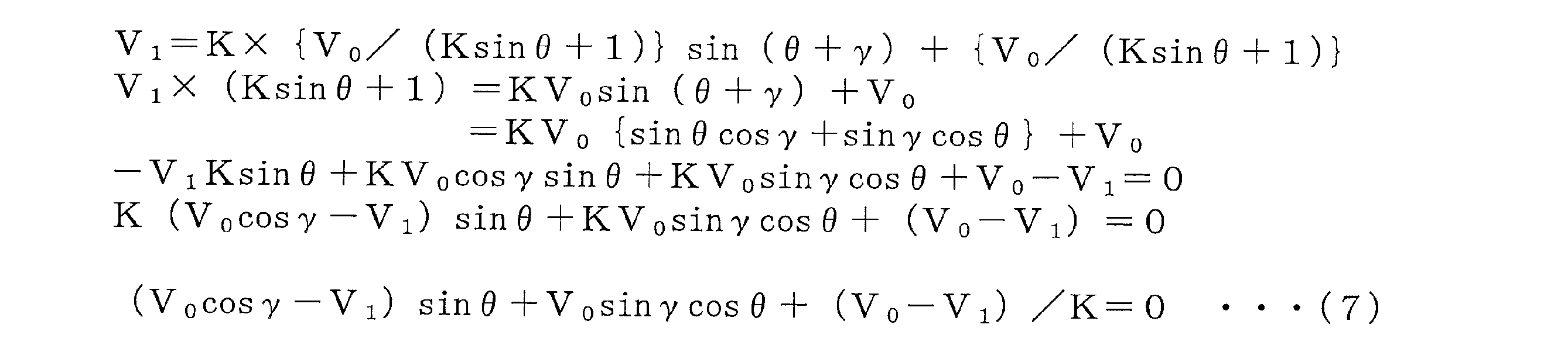
ここで、「V0cosγ-V1=a」、「V0sinγ=b」、「(V0-V1)/K=c」と置くと、上記式(7)は下記式(8)のように表すことができる。
asinθ+bcosθ+c=0 ・・・(8)
ここで、下記[数8]に示すように、上記式(8)を位相θについて解いていくと、下記[数9]に示す下記式(9)を導き出すことができる。
ここで、下記[数8]に示すように、上記式(8)を位相θについて解いていくと、下記[数9]に示す下記式(9)を導き出すことができる。

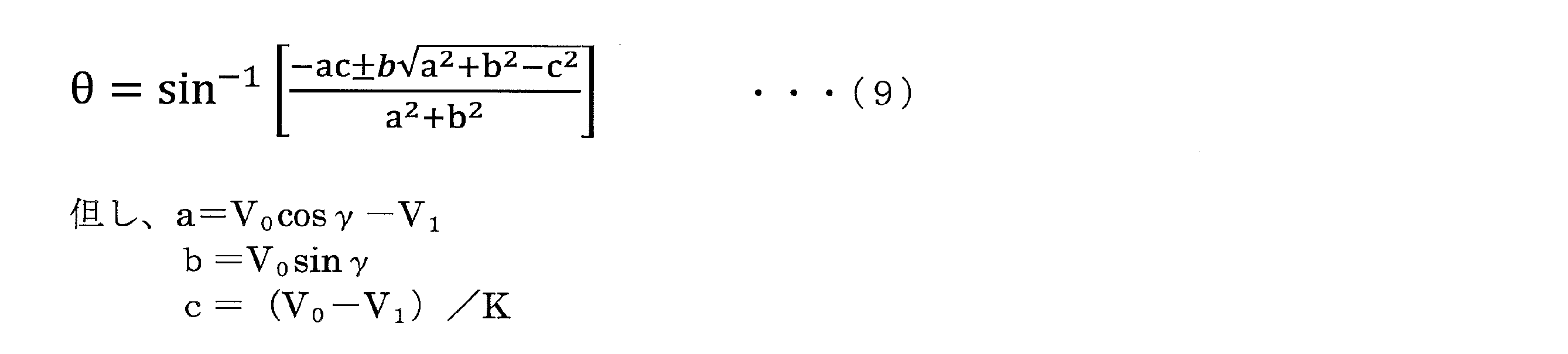
従って、上記手段4における『下記式(1)、(2)、(3)の関係を満たす位相θを算出すること』とあるのは、『下記式(9)に基づき位相θを算出すること』と換言することができる。勿論、位相θを得るアルゴリズムは、上記式(9)に限定されるものではなく、上記式(1)、(2)、(3)の関係を満たすものであれば、他の構成を採用してもよい。
手段5.γ=180°としたことを特徴とする手段4に記載の三次元計測装置。
上記手段5によれば、位相が180°異なる2通りの第2光パターンの下で2回の撮像を行うこととなる。
上記式(2)においてγ=180°とすることで下記式(10)が導き出される。
V1=Asin(θ+180°)+B
=-Asinθ+B ・・・(10)
そして、上記式(1),(10)から下記式(11)を導き出すことができ、これをオフセットBについて解くと、下記式(12)を導き出すことができる。
=-Asinθ+B ・・・(10)
そして、上記式(1),(10)から下記式(11)を導き出すことができ、これをオフセットBについて解くと、下記式(12)を導き出すことができる。
V0+V1=2B ・・・(11)
B=(V0+V1)/2 ・・・(12)
さらに、上記式(12)を上記式(3)に代入することにより、下記式(13)を導き出すことができる。
B=(V0+V1)/2 ・・・(12)
さらに、上記式(12)を上記式(3)に代入することにより、下記式(13)を導き出すことができる。
A=KB
=K(V0+V1)/2 ・・・(13)
また、上記式(1)を「sinθ」について整理すると、下記式(1´)のようになる。
=K(V0+V1)/2 ・・・(13)
また、上記式(1)を「sinθ」について整理すると、下記式(1´)のようになる。
sinθ=(V0-B)/A ・・・(1´)
そして、上記式(1´)に、上記式(12),(13)を代入することにより、下記式(14)を導き出すことができる。
そして、上記式(1´)に、上記式(12),(13)を代入することにより、下記式(14)を導き出すことができる。
sinθ={V0-(V0+V1)/2}/{K(V0+V1)/2}
=(V0-V1)/K(V0+V1) ・・・(14)
ここで、上記式(14)を位相θについて解くと、下記式(15)を導き出すことができる。
=(V0-V1)/K(V0+V1) ・・・(14)
ここで、上記式(14)を位相θについて解くと、下記式(15)を導き出すことができる。
θ=sin-1[(V0-V1)/K(V0+V1)] ・・・(15)
つまり、位相θは、既知の輝度値V0,V1及び定数Kにより特定することができる。
つまり、位相θは、既知の輝度値V0,V1及び定数Kにより特定することができる。
このように、上記手段5によれば、比較的簡単な演算式に基づいて位相θを求めることができ、被計測物の三次元計測を行うに際し、さらなる処理の高速化が可能となる。
手段6.γ=90°としたことを特徴とする手段4に記載の三次元計測装置。
上記手段6によれば、位相が90°異なる2通りの第2光パターンの下で2回の撮像を行うこととなる。
上記式(2)においてγ=90°とすることで下記式(16)が導き出される。
V1=Asin(θ+90°)+B
=Acosθ+B ・・・(16)
上記式(16)を「cosθ」について整理すると、下記式(17)のようになる。
=Acosθ+B ・・・(16)
上記式(16)を「cosθ」について整理すると、下記式(17)のようになる。
cosθ=(V1-B)/A ・・・(17)
また、上記式(1)を「sinθ」について整理すると、上述したように下記式(1´)のようになる。
また、上記式(1)を「sinθ」について整理すると、上述したように下記式(1´)のようになる。
sinθ=(V0-B)/A ・・・(1´)
次に上記式(1´)、(17)を下記式(18)に代入すると下記式(19)のようになり、さらにこれを整理することで、下記式(20)が導き出される。
次に上記式(1´)、(17)を下記式(18)に代入すると下記式(19)のようになり、さらにこれを整理することで、下記式(20)が導き出される。
sin2θ+cos2θ=1 ・・・(18)
{(V0-B)/A}2+{(V1-B)/A}2=1 ・・・(19)
(V0-B)2+(V1-B)2=A2 ・・・(20)
そして、上記式(20)に対し上記式(3)を代入すると下記式(21)のようになり、さらにこれを整理することで、下記式(22)が導き出される。
{(V0-B)/A}2+{(V1-B)/A}2=1 ・・・(19)
(V0-B)2+(V1-B)2=A2 ・・・(20)
そして、上記式(20)に対し上記式(3)を代入すると下記式(21)のようになり、さらにこれを整理することで、下記式(22)が導き出される。
(V0-B)2+(V1-B)2=K2B2 ・・・(21)
(2-K2)B2-2(V0+V1)B+V0 2V1 2=0 ・・・(22)
ここで、上記式(22)をオフセットBについて解くと、下記式(23)を導き出すことができる。
(2-K2)B2-2(V0+V1)B+V0 2V1 2=0 ・・・(22)
ここで、上記式(22)をオフセットBについて解くと、下記式(23)を導き出すことができる。

つまり、オフセットBは、既知の輝度値V0,V1及び定数Kにより特定することができる。
また、下記式(24)に上記式(1´)、(17)を代入すると下記式(25)のようになり、さらにこれを整理することで、下記式(26)が導き出される。
tanθ=sinθ/cosθ ・・・(24)
={(V0-B)/A}/{(V1-B)/A} ・・・(25)
=(V0-B)/(V1-B) ・・・(26)
そして、上記式(26)を位相θについて解くと、下記式(27)を導き出すことができる。
={(V0-B)/A}/{(V1-B)/A} ・・・(25)
=(V0-B)/(V1-B) ・・・(26)
そして、上記式(26)を位相θについて解くと、下記式(27)を導き出すことができる。
θ=tan-1{(V0-B)/(V1-B)} ・・(27)
つまり、位相θは、上記式(23)を用いることにより、既知の輝度値V0,V1及び定数Kにより特定することができる。
つまり、位相θは、上記式(23)を用いることにより、既知の輝度値V0,V1及び定数Kにより特定することができる。
このように、上記手段6によれば、「tan-1」を用いた演算式に基づいて位相θを求めることができるため、-180°~180°の360°の範囲で高さ計測可能となり、計測レンジをより大きくすることができる。
手段7.前記第1計測対象領域及び前記第2計測対象領域のうちの一方が検査対象領域であり、他方が計測基準領域であることを特徴とする手段1乃至6のいずれかに記載の三次元計測装置。
上記手段7によれば、計測基準領域を基準面として検査対象領域に係る計測をより適正に行うことができ、計測精度の向上を図ることができる。但し、「検査対象領域」の計測精度をより高める上では、撮像回数の多い第1計測対象領域が「検査対象領域」となることが好ましい。
手段8.前記被計測物が、クリーム半田が印刷されたプリント基板、又は、半田バンプが形成されたウエハ基板であることを特徴とする手段1乃至7のいずれかに記載の三次元計測装置。
上記手段8によれば、プリント基板に印刷されたクリーム半田、又は、ウエハ基板に形成された半田バンプの高さ計測等を行うことができる。ひいては、クリーム半田又は半田バンプの検査において、その計測値に基づいてクリーム半田又は半田バンプの良否判定を行うことができる。従って、かかる検査において、上記各手段の作用効果が奏されることとなり、精度よく良否判定を行うことができる。結果として、半田印刷検査装置又は半田バンプ検査装置における検査精度の向上を図ることができる。
例えば被計測物をプリント基板とすれば、上記「検査対象領域(例えば第1計測対象領域)」は、クリーム半田が印刷された「半田領域」であることが考えられる。また、「計測基準領域(例えば第2計測対象領域)」は、半田領域以外の「背景領域」であることが考えられる。ここで「背景領域」は、クリーム半田の印刷されていない電極パターンが露出した部分であったり、ガラスエポキシ樹脂等からなるベース基板が露出した部分であったり、電極パターン上を覆うレジスト膜の部分であったり、ベース基板上を覆うレジスト膜の部分であったりすることが考えられる。
〔第1実施形態〕
以下、一実施形態について図面を参照しつつ説明する。まず検査対象となる被計測物としてのプリント基板の構成について詳しく説明する。
以下、一実施形態について図面を参照しつつ説明する。まず検査対象となる被計測物としてのプリント基板の構成について詳しく説明する。
図2に示すように、プリント基板1は、ガラスエポキシ樹脂等からなる平板状のベース基板2に、銅箔からなる電極パターン3が設けられている。さらに、所定の電極パターン3上には、クリーム半田4が印刷されている。
以下、このクリーム半田4が印刷された領域を「半田領域」という。また、半田領域以外の部分を「背景領域」と総称するが、この背景領域には、電極パターン3が露出した領域(記号PA)、ベース基板2が露出した領域(記号PB)、ベース基板2上にレジスト膜5がコーティングされた領域(記号PC)、及び、電極パターン3上にレジスト膜5がコーティングされた領域(記号PD)が含まれる。尚、レジスト膜5は、所定配線部分以外にクリーム半田4がのらないように、プリント基板1の表面にコーティングされるものである。
次に、本実施形態における三次元計測装置を具備する基板検査装置8について詳しく説明する。図1は、基板検査装置8を模式的に示す概略構成図である。同図に示すように、基板検査装置8は、プリント基板1を載置するための載置台9と、プリント基板1の表面に対し斜め上方から所定の光パターンを照射する照射手段としての照明装置10と、プリント基板1上の前記光パターンの照射された部分を撮像するための撮像手段としてのカメラ11と、基板検査装置8内における各種制御や画像処理、演算処理を実施するための制御装置12とを備えている。
載置台9には、モータ15,16が設けられており、該モータ15,16が制御装置12により駆動制御されることによって、載置台9上に載置されたプリント基板1が任意の方向(X軸方向及びY軸方向)へスライドさせられるようになっている。
照明装置10は、光源10aと、該光源10aからの光を正弦波状(縞状)の光強度分布を有する光パターンに変換する液晶格子10bとを備えており、プリント基板1に対し、斜め上方から複数通りに位相変化する縞状の光パターンを照射可能となっている。
より詳しくは、照明装置10において、光源10aから発せられた光は光ファイバーにより一対の集光レンズに導かれ、そこで平行光にされる。その平行光が、液晶格子10bを介して投影レンズに導かれる。そして、投影レンズからプリント基板1に対し縞状の光パターンが照射される。
さらに、照明装置10は、光源10aから発せられる光の輝度を変更可能に構成されている。本実施形態では、後述する輝度設定処理が行われることにより、少なくとも半田領域に応じた半田用輝度と、背景領域に応じた背景用輝度とに切換可能となる。ここで「半田用輝度」が本実施形態における「第1輝度」に相当し、「背景用輝度」が本実施形態における「第2輝度」に相当する。
液晶格子10bは、一対の透明基板間に液晶層が形成されると共に、一方の透明基板上に配置された共通電極と、これと対向するように他方の透明基板上に複数並設された帯状電極とを備え、駆動回路により、各帯状電極にそれぞれ接続されたスイッチング素子(薄膜トランジスタ等)をオンオフ制御し、各帯状電極に印加される電圧を制御することにより、各帯状電極に対応する各格子ラインの光透過率が切替えられ、光透過率の高い「明部」と、光透過率の低い「暗部」とからなる縞状の格子パターンを形成する。そして、液晶格子10bを介してプリント基板1上に照射される光は、回折作用に起因したボケ等により、正弦波状の光強度分布を有する光パターンとなる。
カメラ11は、レンズや撮像素子等からなる。撮像素子としては、CMOSセンサを採用している。勿論、撮像素子はこれに限定されるものではなく、例えばCCDセンサ等を採用してもよい。カメラ11によって撮像された画像データは、該カメラ11内部においてデジタル信号に変換された上で、デジタル信号の形で制御装置12に入力され、後述するデータ記憶装置24に記憶される。そして、制御装置12は、該画像データを基に、後述するような画像処理や検査処理等を実施する。かかる意味で、制御装置12は画像処理手段を構成する。
次に、制御装置12の電気的構成について説明する。図3に示すように、制御装置12は、基板検査装置8全体の制御を司るCPU及び入出力インターフェース21(以下、「CPU等21」という)と、キーボードやマウス、あるいは、タッチパネルで構成される「入力手段」としての入力装置22と、CRTや液晶などの表示画面を有する「表示手段」としての表示装置23と、カメラ11により撮像された画像データや各種演算データなどを記憶するためのデータ記憶装置24と、クリーム半田4などの高さや体積の計測を行う「三次元演算手段」としての三次元演算装置25と、検査結果を記憶するための検査結果記憶装置26と、検査に必要な各種データを予め記憶するデータベース27とを備えている。尚、これら各装置22~27は、CPU等21に対し電気的に接続されている。
データベース27は、半田領域(クリーム半田4の種類)とそれに応じた照明装置10の輝度との対応関係を示す半田用テーブル27A、及び、背景領域(プリント基板1の種類)とそれに応じた照明装置10の輝度との対応関係を示す基板用テーブル27Bを記憶している。
本実施形態では、半田用テーブル27Aは、図4(a)に示すように、a社、b社、c社などの半田領域に印刷されたクリーム半田4の製造メーカと、それらに応じた照明装置10の輝度との対応関係を示すものとなっている。また、基板用テーブル27Bは、図4(b)に示すように、緑、青、黒などの背景領域の色と、それらに応じた照明装置10の輝度との対応関係を示すものとなっている。
次に、制御装置12によって実行される、照明装置10の輝度を設定するための輝度設定処理について、図5のフローチャート及び図6、図7の説明図に基づき説明する。この輝度設定処理は、表示装置23の表示画面に表示される「設定」ボタンが選択操作されることで繰り返し実行されるものである。「設定」ボタンの選択操作は、入力装置22を介してなされるが、例えばマウス等のポインティングデバイスで選択操作されたり、あるいは、表示装置23と一体に構成されたタッチパネルで選択操作されたりする構成として実現される。
最初のステップ(以下、ステップを単に記号Sで示す)100において、検査対象となるプリント基板1の品種が入力されたか否かを判断する。プリント基板1は、ここで指定される品種ごとに検査領域などが設定されているものとする。ここで品種が入力されたと判断された場合(S100:YES)、S110にて品種情報を表示し、S120へ移行する。一方、品種が入力されていないと判断された場合(S100:NO)、以降の処理を実行せず、本輝度設定処理を一旦終了する。
S110における品種情報の表示例を図6に示す。ここでは例えば「品種J」が選択された場合を示している。具体的には、ウインドウW1が表示されている。このウインドウW1は、ウインドウW2,W3から構成されている。ウインドウW2には半田領域の情報が表示され、ウインドウW3には背景領域の情報が表示される。いずれのウインドウW2,W3にも、プリント基板1の全体画像PG1,PG2が表示される。なお、この全体画像PG1,PG2は予め用意されているものとする。もちろん、カメラ11による撮像に基づいて全体画像PG1,PG2を取得するようにしてもよい。
そして、ウインドウW2に表示される半田用の画像PG1には、クリーム半田4の印刷された半田領域であり、検査対象となる検査対象領域31(ウインドウW2中で斜線を施して示した領域)が表示されている。ここで「検査対象領域31」が本実施形態における「第1計測対象領域」に相当する。
一方、ウインドウW3に表示される背景用の画像PG2には、背景領域の一部であって、高さ計測等の基準となる計測基準領域32(ウインドウW3中において斜線を施して示した領域)が表示されている。ここで「計測基準領域32」が本実施形態における「第2計測対象領域」に相当する。
また、ウインドウW2には半田用輝度の入力欄33が表示され、ウインドウW3には背景用輝度の入力欄34が表示される。これらの入力欄33,34には、輝度値がデフォルト表示されるようにしてもよいし、S110の段階では入力欄33,34を空欄にして表示するようにしてもよい。
図5の説明に戻り、S120では、半田用輝度の入力欄33が選択されたか否かを判断する。半田用輝度の入力欄33の選択は、入力装置22を介した選択操作によりなされる。すなわち、上述した「設定」ボタンの選択操作と同様、例えばマウス等のポインティングデバイスで選択操作されたり、あるいは、例えば表示装置23と一体に構成されたタッチパネルで選択操作されたりする構成が考えられる。以下、表示画面上での選択操作については同様とする。ここで入力欄33が選択されたと判断された場合(S120:YES)、S130にて選択リスト(これについては後述する)を表示し、S140へ移行する。一方、入力欄33が選択されていないと判断された場合(S120:NO)、S160へ移行する。
S140では、選択リストから輝度値が選択されたか否かを判断する。ここで輝度値が選択されたと判断された場合(S140:YES)、S150にて半田用輝度の設定処理を行い、S160へ移行する。一方、輝度値が選択されないうちは(S140:NO)、この判断処理を繰り返す。もちろん、所定時間経過しても選択されないような場合には、処理を終了してもよいし、警告等を行ってもよい(S180においても同様)。
S160では、背景用輝度の入力欄34が選択されたか否かを判断する。背景用輝度の入力欄34の選択は、入力装置22を介した選択操作によりなされる。ここで入力欄34が選択されたと判断された場合(S160:YES)、S170にて、後述する選択リストを表示し、S180へ移行する。一方、入力欄34が選択されていないと判断された場合(S160:NO)、S200へ移行する。
S180では、選択リストから輝度値が選択されたか否かを判断する。ここで輝度値が選択されたと判断された場合(S180:YES)、S190にて背景用輝度の設定処理を行い、S200へ移行する。一方、輝度値が選択されないうちは(S180:NO)、この判断処理を繰り返す。
S200では、終了指示があったか否かを判断する。この終了指示は、図示しない画面上の「終了」ボタンの選択操作によってなされる。ここで終了指示があったと判断された場合(S200:YES)、本輝度設定処理を終了する。一方、終了指示がないと判断された場合(S200:NO)、S120からの処理を繰り返す。
次に上述した輝度値の選択及び設定(S120~190)について、具体例を挙げて説明する。なお、ここでは背景用輝度の選択及び設定(S160~S190)について説明するが、半田用輝度の選択及び設定(S120~150)も同様となる。
図6に示した品種Jのプリント基板1の情報表示を前提にして説明する。S170における選択リストの表示は、例えば図7に示す態様で行われる。すなわち、背景用輝度の入力欄34が選択されると(S160:YES)、新たなウインドウW4が入力欄34の下側に表示される。表示される選択リストの内容は、図4(b)に示した基板用テーブルにおける色と輝度との対応関係である。そして、この選択リスト中の輝度値(図中に黒三角などで示した)が選択されると(S180:YES)、該輝度値が設定されて(S190)、背景用輝度の入力欄34に表示される。なお、S180では輝度値を選択させるようにしているが、「緑」、「青」、「黒」などと示される基板種類(色)を選択させるようにしてもよいし、あるいは、それら輝度値及び基板種類のいずれか一方を選択させるようにしてもよい。
このようにして半田用輝度及び背景用輝度の設定が終了すると、プリント基板1の検査が開始可能となる。
次に基板検査装置8よるプリント基板1の検査手順について、各検査エリアごとに行われる検査ルーチンを基に詳しく説明する。この検査ルーチンは、制御装置12(CPU等21)にて実行されるものである。
制御装置12は、まずモータ15,16を駆動制御してプリント基板1を移動させ、カメラ11の視野をプリント基板1上の所定の検査エリア(計測範囲)に合わせる。なお、検査エリアは、カメラ11の視野の大きさを1単位としてプリント基板1の表面を予め分割しておいた中の1つのエリアである。
続いて、制御装置12は、照明装置10の設定処理を行う。より詳しくは、光源10aの輝度の切換制御処理と、液晶格子10bの切換制御処理を行う。具体的には、光源10aから照射される光の輝度を、上記輝度設定処理により事前に定めた半田用輝度(第1輝度)に切換設定すると共に、液晶格子10bを切換制御し、該液晶格子10bに形成される格子の位置を所定の基準位置(位相「0°」)に設定する。従って、制御装置12による光源10aの輝度の切換制御処理を行う機能により本実施形態における「輝度制御手段」が構成され、液晶格子10bの切換制御処理を行う機能により「位相制御手段」が構成される。
光源10a及び液晶格子10bの切換設定が完了すると、制御装置12は、照明装置10の光源10aを発光させ、半田用輝度の第1光パターンの照射を開始すると共に、該第1光パターンの位相を90°ずつ、4通りの位相(位相「0°」、位相「90°」、位相「180°」、位相「270°」)に順次シフトする。
そして、制御装置12は、第1光パターンの位相が順次シフトされる毎にカメラ11を駆動制御して、該第1光パターンが照射された検査エリア部分を撮像する。これにより、所定の検査エリアに関して、位相を90°ずつシフトさせた第1光パターンの下で撮像された4通りの画像データが取得される。ここで、カメラ11により撮像された画像データはデータ記憶装置24へ転送され記憶される。
続いて、制御装置12(三次元演算装置25)は、位相シフト法により、上記4通りの画像データ(輝度値)から各画素に係る第1光パターンの位相θ1を算出する。
ここで、上記4通りの画像データの各画素に係る輝度値V10,V11,V12,V13は、下記式(H1)、(H2)、(H3)、(H4)により表すことができる。

上記式(H1)、(H2)、(H3)、(H4)を位相θ1について解くと、下記式(H5)を導き出すことができる。

そして、上記のように算出された位相θ1を用いて、三角測量の原理に基づき、検査対象領域31の各画素(x,y)に係る高さデータ(z)を算出し、かかる高さデータ(z)を検査結果記憶装置26に記憶する。従って、これら一連の処理機能により本実施形態における第1計測手段が構成される。
次に第1光パターンの下で撮像された上記4通りの画像データから各画素に係るゲインA1及びオフセットB1の関係を把握し、これをデータ記憶装置24に記憶する。従って、かかる処理機能により本実施形態における関係把握手段が構成される。但し、ゲインA1及びオフセットB1の関係を把握する処理は、上記4通りの画像データの取得後(撮像後)、上述した検査対象領域31に係る高さデータの算出処理と並行して行われる。
ここでゲインA1及びオフセットB1の関係、すなわちゲインA1及びオフセットB1の比例定数Kを算出する手順についてより詳しく説明する。4通りの画像データの各画素に係る輝度値V10,V11,V12,V13と、ゲインA1及びオフセットB1との関係は、上記式(H1)~(H4)のとおりである。
ここで、4通りの画像データの輝度値V10,V11,V12,V13を加算し、上記式(H1)~(H4)を下記[数13]に示すように整理すると、下記式(H6)を導き出すことができる。

また、上記式(H1)、(H3)から、下記式(H7)を導き出すことができる。

また、上記式(H2)、(H4)から、下記式(H8)を導き出すことができる。

そして、下記[数16]に示すように、上記式(H7)、(H8)を下記式(H9)に代入し、整理していくと、下記式(H10)を導き出すことができる。

さらに、上記式(H6)、(H10)から導き出された下記式(H11)を基にゲインA1及びオフセットB1の比例定数Kを算出する。

このように算出された各画素に係るゲインA1及びオフセットB1の比例定数Kをデータ記憶装置24に記憶する。
次に制御装置12は、計測基準領域32に係る撮像処理を開始する。但し、計測基準領域32に係る撮像処理は、検査対象領域31に係る一連の撮像処理の終了後、直ちに開始される。つまり、上述した検査対象領域31に係る高さデータの算出処理、並びに、ゲインA1及びオフセットB1の比例定数Kの算出処理と並行して行われる。
より詳しくは、光源10aの輝度の切換制御処理と、液晶格子10bの切換制御処理を行う。具体的には、光源10aから照射される光の輝度を、上記輝度設定処理により事前に定めた背景用輝度(第2輝度)に切換設定すると共に、液晶格子10bを切換制御し、該液晶格子10bに形成される格子の位置を所定の基準位置(位相「0°」)に設定する。
光源10a及び液晶格子10bの切換設定が完了すると、制御装置12は、照明装置10の光源10aを発光させ、背景用輝度の第2光パターンの照射を開始すると共に、該第2光パターンの位相を2通りの位相(位相「0°」、位相「180°」)に順次シフトする。
そして、制御装置12は、第2光パターンの位相が順次シフトされる毎にカメラ11を駆動制御して、該第2光パターンが照射された検査エリア部分を撮像する。これにより、所定の検査エリアに関して、位相を180°シフトさせた第2光パターンの下で撮像された2通りの画像データが取得される。ここで、カメラ11により撮像された画像データはデータ記憶装置24へ転送され記憶される。
続いて、制御装置12は、上記2通りの画像データを基に、位相シフト法により、計測基準領域32の各画素に係る第2光パターンの位相θ2を算出する。
具体的に、第2光パターンの位相θ2は、上記2通りの画像データの各画素に係る輝度値をそれぞれV20,V21とした場合、上記式(15)を基に、下記式(15´)のように表すことができる。
θ2=sin-1[(V20-V21)/K(V20+V21)] ・・・(15´)
但し、K:比例定数。
但し、K:比例定数。
尚、本実施形態では、第2光パターンの下で撮像された上記2通りの画像データの各画素に係るゲインA2及びオフセットB2の関係(比例定数K=A2/B2)と、第1光パターンの下で撮像された上記4通りの画像データの各画素に係るゲインA1及びオフセットB1の関係(比例定数K=A1/B1)は等しいため、ここの比例定数Kには、データ記憶装置24に記憶された既知の値が用いられる〔上記式(H11)参照〕。
そして、上記のように算出された位相θ2を用いて、三角測量の原理に基づき、計測基準領域32の各画素(x,y)に係る高さデータ(z)を算出し、かかる高さデータ(z)を検査結果記憶装置26に記憶する。従って、これら一連の処理機能により本実施形態における第2計測手段が構成される。
続いて、制御装置12は、計測基準領域32を高さ基準面として検査対象領域31のクリーム半田4の高さや体積、印刷範囲などを算出する。そして、制御装置12は、このようにして求めたクリーム半田4の位置、面積、高さ又は体積等のデータを、予め記憶した基準データと比較判定し、この比較結果が許容範囲内にあるか否かによって、その検査エリアにおけるクリーム半田4の印刷状態の良否を判定する。かかる検査結果は、検査結果記憶装置26に記憶される。
かかる処理が行われている間に、制御装置12は、モータ15,16を駆動制御してプリント基板1を次の検査エリアへと移動せしめ、以降、上記一連の処理が、全ての検査エリアで繰り返し行われることで、プリント基板1全体の検査が終了する。
以上詳述したように、本実施形態によれば、検査対象領域31に応じた第1輝度の第1光パターンを照射し撮像された画像データを基に該検査対象領域31に係る三次元計測を行うと共に、計測基準領域32に応じた第2輝度の第2光パターンを照射し撮像された画像データを基に該計測基準領域32に係る三次元計測を行う構成となっている。これにより、検査対象領域31及び計測基準領域32の両者とも、輝度を変えて、それぞれ適正な輝度の光パターンの下で撮像した画像データに基づき三次元計測を行うことができる。結果として、計測精度の低下抑制を図ることができる。
さらに、本実施形態では、検査対象領域31の計測を目的として撮像された4通りの画像データから、所定の撮像条件により定まる光パターンのゲインA及びオフセットBの関係(比例定数K)を把握すると共に、かかる光パターンのゲインA及びオフセットBの関係と、画像データ上の各画素に係る輝度値Vから定まる、該画素に係る光パターンのゲインA又はオフセットBの値とを利用することにより、計測基準領域32に関しては、2通りに位相変化させた光パターンの下で撮像した2通りの画像データを基に位相シフト法により三次元計測を行うことができる。
つまり、本実施形態によれば、第1輝度の第1光パターンを4通りの位相で照射し、その下で4通りの画像を撮像した後、第2輝度の第2光パターンを2通りの位相で照射し、その下で2通りの画像を撮像すればよいため、撮像回数が計6回となり、撮像時間が大幅に減少する。
従って、従来技術に比べ、総合的な撮像回数が少なくて済み、撮像時間を短縮することができる。結果として、計測時間を飛躍的に短縮することができる。
尚、本実施形態では、計測基準領域32に関して、位相が180°異なる2通りの画像データを基に三次元計測が行われる構成となっているため、計測レンジが-90°~90°の180°の範囲と比較的狭いものとなってしまうが、基準面となる計測基準領域32は、平坦でその高さが略均一であるため、計測レンジが狭くても特段の支障はない。
加えて、本実施形態では、図4(b)の基板用テーブル27Bにおいて、基板種類(基板色)が「黒」の場合に対応する輝度も用意されている。これは、計測基準領域32(背景領域)が黒色あるいは相対的に黒色に近い灰色である場合、検査対象領域31に応じた輝度で撮像した画像データにおいては、計測基準領域32における明暗の差(輝度差)が小さくなるおそれが高いからである。したがって、本実施形態によれば、計測基準領域32が黒色あるいは相対的に黒色に近い灰色である場合には、効果が際立つ結果となる。
〔第2実施形態〕
以下、第2実施形態について図面を参照しつつ説明する。但し、第1実施形態と重複する同一構成部分については、同一符号を付し、その詳細な説明を省略する。以下、第1実施形態と相違する部分を中心に説明する。
以下、第2実施形態について図面を参照しつつ説明する。但し、第1実施形態と重複する同一構成部分については、同一符号を付し、その詳細な説明を省略する。以下、第1実施形態と相違する部分を中心に説明する。
本実施形態では、検査対象領域31に応じた第1輝度で光パターンを照射し撮像した画像データを基に、計測基準領域32の三次元計測が可能か否かを判断し、三次元計測が不可能と判断された場合には、前記第1輝度を計測基準領域32に応じた第2輝度に補正し、該第2輝度で光パターンを照射する構成となっている。
以下、検査対象領域31及び計測基準領域32の計測に係る一連の撮像処理について、図8のフローチャートを参照して詳しく説明する。
まず最初のステップ(以下、ステップを単に記号Sで示す)200において、照明装置10の輝度をクリーム半田4に合わせて設定する。この輝度は、半田用輝度(第1輝度)として、予め決められたものである。
続くS210では、制御装置12によって、設定された半田用輝度となるように照明装置10が点灯され、プリント基板1の表面に対し斜め上方から第1輝度の第1光パターンが照射される。そして、制御装置12は、第1光パターンの位相が順次シフトされる毎にカメラ11を駆動制御して、該第1光パターンが照射された検査エリア部分を撮像する。これにより、位相を90°ずつシフトさせた第1光パターンの下で撮像された4通りの画像データが取得される。
次のS220では、S210にて撮像された画像データに基づき、背景領域の平均輝度を算出する。
続くS230では、背景領域の目標輝度とS220にて算出された平均輝度との差分がしきい値以上か否かを判断する。ここで差分がしきい値以上であると判断された場合(S230:YES)、S240へ移行する。一方、差分がしきい値を下回っている場合(S230:NO)、以降の処理を実行せず、本撮像処理を終了する。
差分がしきい値以上であると判断された場合に移行するS240では、輝度を補正する。具体的には、S220にて算出された平均輝度と目標輝度との比率に基づき、照明装置10の輝度を補正して設定する。すなわち、半田用輝度(第1輝度)が補正されて背景用輝度(第2輝度)が設定されることになる。
S250では、制御装置12によって、補正された背景用輝度となるように照明装置10が点灯され、プリント基板1の表面に対し斜め上方から第2輝度の第2光パターンが照射される。そして、制御装置12は、第2光パターンの位相が順次シフトされる毎にカメラ11を駆動制御して、該第2光パターンが照射された検査エリア部分を撮像する。これにより、位相を180°シフトさせた第2光パターンの下で撮像された2通りの画像データが取得される。
以上の撮像処理に対する理解を容易にするため、具体例を挙げて説明する。
図9は、背景領域における光パターンの輝度をグラフとして模式的に示すものである。背景領域(計測基準領域32)の三次元計測を行うための理想的な輝度を、グラフ上部に二点鎖線で示した。縞状の光パターンを照射した場合、ある程度の振幅を有するサインカーブとなることが望ましい。ところが、半田領域(検査対象領域31)に合わせた輝度で撮像した場合、背景領域が比較的暗い色である場合など、グラフ下部に実線で示すような振幅の小さなサインカーブとなってしまうことがある。つまり、明暗の差(輝度差)が小さくなってしまうのである。
そこで、上述の撮像処理においては、背景領域の平均輝度を算出し(図8中のS220)、目標輝度との差がしきい値以上であるか否かを判断し(S230)、しきい値以上である場合(S230:YES)、半田用輝度を補正して背景用輝度を設定する(S240)。図9で言えば、背景領域の輝度の平均値、すなわちグラフ下部のサインカーブの平均値Nを算出し(S220)、予め定められる理想的な輝度の平均値である目標値Mとの差分Dが、しきい値以上であるか否かを判断する(S230)。そして、しきい値以上である場合(S230:YES)、目標値Mと平均値Nとの比率に基づいて、半田用輝度を補正して背景用輝度を設定する。具体的には、半田用輝度を(M/N)倍して背景用輝度を設定する。
そして、かかる背景用輝度での照射によって得られた画像データに基づき計測基準領域32の三次元計測を行うと共に、半田用輝度での照射によって得られた画像データに基づき検査対象領域31の三次元計測を行う。
一方、背景用輝度での照明・撮像が行われない場合、制御装置12は、半田用輝度での照射によって得られた画像データに基づき検査対象領域31及び計測基準領域32の三次元計測を行う。
そして、計測基準領域32を高さ基準面として検査対象領域31のクリーム半田4の高さや体積が計測されることになる。
以上詳述したように、本実施形態によれば、上記第1実施形態と同様の作用効果が奏される。
さらに、本実施形態では、クリーム半田4の色が製造メーカによってそれほど異ならないという前提の下、半田領域(検査対象領域31)に合わせて予め決められた半田用輝度で照明装置10が点灯されて撮像が行われる(図8中のS200,S210)。そして、かかる半田用輝度の第1光パターンの下で撮像された画像データに基づいて、検査対象領域31に係る三次元計測が行われる。次に、この第1光パターンの下で撮像された画像データに基づき、背景領域の輝度の平均値を算出し(S220)、輝度の目標値との差分がしきい値以上である場合は(S230:YES)、目標値との比率を用いて半田用輝度を補正して背景用輝度を設定する(S240)。背景用輝度が設定されると、この背景用輝度で照明装置10が点灯されて撮像が行われる(S250)。そして、かかる背景用輝度の第2光パターンの下で撮像された画像データに基づいて、計測基準領域32に係る三次元計測が実行可能となる。
また、上述したように、計測基準領域32(背景領域)が黒色あるいは相対的に黒色に近い灰色である場合、検査対象領域31に応じた輝度で撮像した画像データにおいて、背景領域における明暗の差(輝度差)が小さくなるおそれが高い。このような場合も、実際の輝度の平均値と目標値との比率で補正されて計測基準領域32の三次元計測が実行可能となるため、計測基準領域32が黒色あるいは相対的に黒色に近い灰色である場合には、効果が際立つ結果となる。
尚、上記実施形態の記載内容に限定されず、例えば次のように実施してもよい。勿論、以下において例示しない他の応用例、変更例も当然可能である。
(a)上記実施形態では、三次元計測装置を、プリント基板1に印刷形成されたクリーム半田4の高さ等を計測する基板検査装置8に具体化したが、これに限らず、例えば基板上に印刷された半田バンプや、基板上に実装された電子部品など、他のものの高さを計測する構成に具体化してもよい。例えばウエハ基板の場合には、酸化膜の表面を基準高さとして利用可能となり、半田バンプの高さ、形状、体積等を算出可能となる。
(b)上記実施形態では、光源10aからの光を縞状の光パターンに変換するための格子を、液晶格子10bにより構成すると共に、これを切替制御することにより、光パターンの位相をシフトさせる構成となっている。これに限らず、例えば格子部材をピエゾアクチュエータ等の移送手段により移送させ、光パターンの位相をシフトさせる構成としてもよい。
(c)上記実施形態では、第1光パターンによる第1計測対象領域(検査対象領域31)の計測時において、位相が90°ずつ異なる4通りの第1光パターンの下で撮像された4通りの画像データを基に、位相シフト法により三次元計測を行う構成となっているが、これに限らず、例えば位相が120°ずつ異なる3通りの第1光パターンの下で撮像された3通りの画像データを基に三次元計測を行う構成としてもよい。つまり、第1光パターンの下での第1計測対象領域の撮像回数である「所定数」は、少なくとも位相シフト法により三次元計測を実行可能な数であれば良い。
(d)上記実施形態では、第2光パターンによる第2計測対象領域(計測基準領域32)の計測時において、位相が180°異なる2通りの光パターンの下で撮像された2通りの画像データを基に三次元計測を行う構成となっている。これに代えて、例えば位相が90°異なる2通りの光パターンの下で撮像された2通りの画像データを基に三次元計測を行う構成としてもよい。かかる場合、上記式(23),(27)を用いることにより、2通りの画像データ上の各画素における輝度値V20,V21と、既知の比例定数Kを利用して、各画素における第2光パターンの位相θ2を算出することができる。
かかる構成によれば、「tan-1」を用いた演算式に基づいて位相θ2を求めることができるため、-180°~180°の360°の範囲で高さ計測可能となり、計測レンジをより大きくすることができる。
勿論、この他にも、上記式(1)、(2)、(3)の関係を満たすものであれば、他の構成を採用してもよい。位相θ2を得る一般式としては、上記式(9)が一例に挙げられる〔[数9]参照〕。
(e)ゲインA及びオフセットBの関係を把握する関係把握手段の構成は上記実施形態に限定されるものではない。
例えばゲインAとオフセットBとの関係は、式として求めることなく、ゲインAとオフセットBとの関係を表した数表やテーブルデータを作成することにより、ゲインAからオフセットBあるいはオフセットBからゲインAを求めることが可能に構成しても良い。
(f)上記第1実施形態ではメーカ毎に輝度の異なる半田用テーブル27Aを記憶している構成であったが、半田領域(クリーム半田4の印刷された領域)の色が比較的安定している場合には、半田用テーブル27Aを省略してもよい。すなわち、第2実施形態と同様に、製造メーカ各社で大きな違いがないことに着目し、検査対象領域31の計測を目的とする撮像に際しては、予め決められた輝度で照明装置10を点灯する構成としてもよい。
(g)上記実施形態では、複数個の計測基準領域32(背景領域)に対し、同一の背景用輝度を設定し、当該背景用輝度による照明装置10の照射に基づき撮像を行っている。
これに対し、複数個の計測基準領域32を、異なる輝度での照射によって撮像する構成としてもよい。これは複数個の各計測基準領域32が、同一色であるとは限らないためである。そこで、図10に示すように、品種情報の表示において、各計測基準領域32に対応させてU1~U5などの記号を表示し、各計測基準領域32毎に背景用輝度を設定可能な構成としてもよい。例えばプリント基板1の画像PG2に表示される記号に対応させるようにして入力欄35を用意するという具合である。
(h)上記第2実施形態では、画像データにおける背景領域の輝度の平均値と目標値との比率で半田用輝度を補正していた。このようにすれば比較的簡単な計算式で半田用輝度が補正されることになるが、輝度と画像データの輝度とは、完全には線形比例しない。
そこで、データベース27に予め補正情報を記憶しておくようにしてもよい。補正情報は、例えば背景領域の輝度の平均値に応じた半田用輝度の補正倍率であることが考えられる。そして、第1光パターンによる撮像に基づいて計測基準領域32の三次元計測が不可能と判断された場合、この補正情報を参照して半田用輝度を補正して背景用輝度を設定する。このようにすれば、設定される背景用輝度がより適切なものとなり、背景用輝度での撮像によって、計測基準領域32の三次元計測が確実に実行可能となる。
(i)上記実施形態では、計測基準領域32(背景領域)が黒色あるいは相対的に黒色に近い灰色である場合に効果が際立つ旨上述したが、計測基準領域32(背景領域)が白色あるいは相対的に白色に近い灰色である場合には、検査対象領域31(半田領域)に応じた輝度で撮像した画像データ中において、計測基準領域32(背景領域)における輝度が高くなりすぎて飽和状態となってしまうおそれが高い。したがって、計測基準領域32(背景領域)が白色あるいは相対的に白色に近い灰色である場合にも効果が際立つ結果となる。
1…プリント基板、2…ベース基板、3…電極パターン、4…クリーム半田、5…レジスト膜、8…基板検査装置、10…照明装置、10a…光源、10b…液晶格子、11…カメラ、12…制御装置、24…データ記憶装置、25…三次元演算装置、26…検査結果記憶装置、27…データベース、27A…半田用テーブル、27B…基板用テーブル、31…検査対象領域、32…計測基準領域、A1,A2…ゲイン、B1,B2…オフセット、K…比例定数。
Claims (8)
- 所定の光を発する光源、及び、該光源からの光を縞状の光強度分布を有する光パターンに変換する格子を有し、該光パターンを少なくとも第1計測対象領域及び第2計測対象領域を有する被計測物に対し照射可能な照射手段と、
前記光源から発せられる光の輝度を変更可能な輝度制御手段と、
前記格子の移送又は切替を制御し、前記照射手段から照射する前記光パターンの位相を複数通りに変化可能な位相制御手段と、
前記光パターンの照射された前記被計測物からの反射光を撮像可能な撮像手段と、
前記撮像手段により撮像された画像データを基に位相シフト法により前記被計測物の三次元計測を実行可能な画像処理手段とを備え、
前記画像処理手段は、
前記第1計測対象領域に応じた第1輝度の第1光パターンを所定数通りの位相で照射し撮像された所定数通りの画像データを基に、前記第1計測対象領域に係る三次元計測を行う第1計測手段と、
前記第1光パターンの下で撮像された前記所定数通りの画像データを基に、所定の撮像条件により定まるゲイン及びオフセットの関係を把握する関係把握手段と、
前記第2計測対象領域に応じた第2輝度の第2光パターンを2通りの位相で照射し撮像された2通りの画像データを基に、該2通りの画像データの各画素の輝度値から定まる該画素に係るゲイン又はオフセットの値と、前記関係把握手段により把握されたゲイン及びオフセットの関係とを利用して、前記第2計測対象領域に係る三次元計測を行う第2計測手段とを備えたことを特徴とする三次元計測装置。 - 前記ゲイン及びオフセットの関係は、前記ゲインと前記オフセットとが相互に一義的に定まる関係であることを特徴とする請求項1に記載の三次元計測装置。
- 前記ゲイン及びオフセットの関係は、前記ゲインと前記オフセットとが比例関係であることを特徴とする請求項1に記載の三次元計測装置。
- 前記2通りに位相変化させた第2光パターンの相対位相関係をそれぞれ0、γとしたときの前記2通りの画像データの各画素の輝度値をそれぞれV0、V1とした場合に、
前記第2計測手段は、前記第2計測対象領域に係る計測を行うに際し、
下記式(1)、(2)、(3)の関係を満たす位相θを算出することを特徴とする請求項1乃至3のいずれかに記載の三次元計測装置。
V0=Asinθ+B ・・・(1)
V1=Asin(θ+γ)+B ・・・(2)
A=KB ・・・(3)
但し、γ≠0、A:ゲイン、B:オフセット、K:比例定数。 - γ=180°としたことを特徴とする請求項4に記載の三次元計測装置。
- γ=90°としたことを特徴とする請求項4に記載の三次元計測装置。
- 前記第1計測対象領域及び前記第2計測対象領域のうちの一方が検査対象領域であり、他方が計測基準領域であることを特徴とする請求項1乃至6のいずれかに記載の三次元計測装置。
- 前記被計測物が、クリーム半田が印刷されたプリント基板、又は、半田バンプが形成されたウエハ基板であることを特徴とする請求項1乃至7のいずれかに記載の三次元計測装置。
Priority Applications (3)
| Application Number | Priority Date | Filing Date | Title |
|---|---|---|---|
| CN201680018284.4A CN107407556B (zh) | 2015-06-23 | 2016-01-08 | 三维测量装置 |
| DE112016002874.1T DE112016002874T5 (de) | 2015-06-23 | 2016-01-08 | Vorrichtung zur dreidimensionalen Messung |
| US15/849,911 US10161744B2 (en) | 2015-06-23 | 2017-12-21 | Three-dimensional measurement device |
Applications Claiming Priority (2)
| Application Number | Priority Date | Filing Date | Title |
|---|---|---|---|
| JP2015-125213 | 2015-06-23 | ||
| JP2015125213A JP6110897B2 (ja) | 2015-06-23 | 2015-06-23 | 三次元計測装置 |
Related Child Applications (1)
| Application Number | Title | Priority Date | Filing Date |
|---|---|---|---|
| US15/849,911 Continuation US10161744B2 (en) | 2015-06-23 | 2017-12-21 | Three-dimensional measurement device |
Publications (1)
| Publication Number | Publication Date |
|---|---|
| WO2016208207A1 true WO2016208207A1 (ja) | 2016-12-29 |
Family
ID=57584983
Family Applications (1)
| Application Number | Title | Priority Date | Filing Date |
|---|---|---|---|
| PCT/JP2016/050552 Ceased WO2016208207A1 (ja) | 2015-06-23 | 2016-01-08 | 三次元計測装置 |
Country Status (6)
| Country | Link |
|---|---|
| US (1) | US10161744B2 (ja) |
| JP (1) | JP6110897B2 (ja) |
| CN (1) | CN107407556B (ja) |
| DE (1) | DE112016002874T5 (ja) |
| TW (1) | TWI568988B (ja) |
| WO (1) | WO2016208207A1 (ja) |
Families Citing this family (9)
| Publication number | Priority date | Publication date | Assignee | Title |
|---|---|---|---|---|
| JP6306230B1 (ja) * | 2017-02-09 | 2018-04-04 | Ckd株式会社 | 半田印刷検査装置、半田印刷検査方法、及び、基板の製造方法 |
| JP7083695B2 (ja) * | 2018-05-11 | 2022-06-13 | 株式会社荏原製作所 | バンプ高さ検査装置、基板処理装置、バンプ高さ検査方法、記憶媒体 |
| JP2020091132A (ja) * | 2018-12-04 | 2020-06-11 | 株式会社小糸製作所 | 透光性部材の表面欠陥検査装置 |
| WO2020170328A1 (ja) * | 2019-02-19 | 2020-08-27 | 株式会社Fuji | 部品装着機 |
| JP7030079B2 (ja) * | 2019-06-12 | 2022-03-04 | Ckd株式会社 | 三次元計測装置及び三次元計測方法 |
| CN113743145B (zh) * | 2020-05-29 | 2023-10-20 | 长鑫存储技术有限公司 | 编码采集系统及方法 |
| CN112179288B (zh) * | 2020-08-19 | 2022-09-20 | 成都飞机工业(集团)有限责任公司 | 基于折射偏光强度信息的零件外形测量装置及测量方法 |
| KR102844432B1 (ko) * | 2020-08-24 | 2025-08-11 | 삼성디스플레이 주식회사 | 표시 패널 검사용 지그 |
| JP7653039B2 (ja) * | 2021-02-24 | 2025-03-28 | 株式会社デンソーウェーブ | 三次元計測システム |
Citations (4)
| Publication number | Priority date | Publication date | Assignee | Title |
|---|---|---|---|---|
| JP2006300539A (ja) * | 2005-04-15 | 2006-11-02 | Ckd Corp | 三次元計測装置及び基板検査装置 |
| JP2009115612A (ja) * | 2007-11-06 | 2009-05-28 | Panasonic Electric Works Co Ltd | 3次元形状計測装置及び3次元形状計測方法 |
| JP2010243438A (ja) * | 2009-04-09 | 2010-10-28 | Nikon Corp | 三次元形状測定装置及び三次元形状測定方法 |
| JP2012053015A (ja) * | 2010-09-03 | 2012-03-15 | Saki Corp:Kk | 外観検査装置及び外観検査方法 |
Family Cites Families (12)
| Publication number | Priority date | Publication date | Assignee | Title |
|---|---|---|---|---|
| US5848188A (en) * | 1994-09-08 | 1998-12-08 | Ckd Corporation | Shape measure device |
| JP3878023B2 (ja) * | 2002-02-01 | 2007-02-07 | シーケーディ株式会社 | 三次元計測装置 |
| TWI291013B (en) * | 2006-01-25 | 2007-12-11 | Univ Nat Taipei Technology | Digital-structured micro-optic three-dimensional confocal surface profile measuring system and technique |
| JP5137526B2 (ja) * | 2006-12-22 | 2013-02-06 | キヤノン株式会社 | 形状測定装置、形状測定方法、および露光装置 |
| JP2010164350A (ja) * | 2009-01-14 | 2010-07-29 | Ckd Corp | 三次元計測装置 |
| JP4744610B2 (ja) * | 2009-01-20 | 2011-08-10 | シーケーディ株式会社 | 三次元計測装置 |
| JP2010185844A (ja) * | 2009-02-13 | 2010-08-26 | Tokyo Institute Of Technology | 表面形状測定方法およびこれを用いた装置 |
| JP4715944B2 (ja) * | 2009-04-03 | 2011-07-06 | オムロン株式会社 | 三次元形状計測装置、三次元形状計測方法、および三次元形状計測プログラム |
| DE102010030883B4 (de) * | 2009-07-03 | 2018-11-08 | Koh Young Technology Inc. | Vorrichtung zur Prüfung einer Platte und Verfahren dazu |
| JP6029394B2 (ja) * | 2012-09-11 | 2016-11-24 | 株式会社キーエンス | 形状測定装置 |
| JP2014228486A (ja) * | 2013-05-24 | 2014-12-08 | インスペック株式会社 | 三次元プロファイル取得装置、パターン検査装置及び三次元プロファイル取得方法 |
| JP6695746B2 (ja) * | 2016-06-27 | 2020-05-20 | 株式会社キーエンス | 測定装置 |
-
2015
- 2015-06-23 JP JP2015125213A patent/JP6110897B2/ja active Active
- 2015-12-23 TW TW104143282A patent/TWI568988B/zh active
-
2016
- 2016-01-08 CN CN201680018284.4A patent/CN107407556B/zh active Active
- 2016-01-08 DE DE112016002874.1T patent/DE112016002874T5/de active Pending
- 2016-01-08 WO PCT/JP2016/050552 patent/WO2016208207A1/ja not_active Ceased
-
2017
- 2017-12-21 US US15/849,911 patent/US10161744B2/en active Active
Patent Citations (4)
| Publication number | Priority date | Publication date | Assignee | Title |
|---|---|---|---|---|
| JP2006300539A (ja) * | 2005-04-15 | 2006-11-02 | Ckd Corp | 三次元計測装置及び基板検査装置 |
| JP2009115612A (ja) * | 2007-11-06 | 2009-05-28 | Panasonic Electric Works Co Ltd | 3次元形状計測装置及び3次元形状計測方法 |
| JP2010243438A (ja) * | 2009-04-09 | 2010-10-28 | Nikon Corp | 三次元形状測定装置及び三次元形状測定方法 |
| JP2012053015A (ja) * | 2010-09-03 | 2012-03-15 | Saki Corp:Kk | 外観検査装置及び外観検査方法 |
Also Published As
| Publication number | Publication date |
|---|---|
| DE112016002874T5 (de) | 2018-03-08 |
| US20180112974A1 (en) | 2018-04-26 |
| TW201700952A (zh) | 2017-01-01 |
| TWI568988B (zh) | 2017-02-01 |
| CN107407556A (zh) | 2017-11-28 |
| JP2017009442A (ja) | 2017-01-12 |
| CN107407556B (zh) | 2019-11-05 |
| US10161744B2 (en) | 2018-12-25 |
| JP6110897B2 (ja) | 2017-04-05 |
Similar Documents
| Publication | Publication Date | Title |
|---|---|---|
| JP6110897B2 (ja) | 三次元計測装置 | |
| JP5290233B2 (ja) | 三次元計測装置及び基板検査装置 | |
| JP6109255B2 (ja) | 三次元計測装置 | |
| JP5430612B2 (ja) | 三次元計測装置 | |
| JP5640025B2 (ja) | 三次元計測装置 | |
| JP5957575B1 (ja) | 三次元計測装置 | |
| JP6791631B2 (ja) | 画像生成方法及び検査装置 | |
| WO2012124260A1 (ja) | はんだ高さ検出方法およびはんだ高さ検出装置 | |
| JP4827431B2 (ja) | 三次元計測装置及び基板検査装置 | |
| CN113966457B (zh) | 三维测量装置和三维测量方法 | |
| JP6027204B1 (ja) | 三次元計測装置 | |
| JP6126640B2 (ja) | 三次元計測装置及び三次元計測方法 | |
| WO2016203668A1 (ja) | 三次元計測装置 |
Legal Events
| Date | Code | Title | Description |
|---|---|---|---|
| 121 | Ep: the epo has been informed by wipo that ep was designated in this application |
Ref document number: 16813978 Country of ref document: EP Kind code of ref document: A1 |
|
| WWE | Wipo information: entry into national phase |
Ref document number: 112016002874 Country of ref document: DE |
|
| 122 | Ep: pct application non-entry in european phase |
Ref document number: 16813978 Country of ref document: EP Kind code of ref document: A1 |