WO2016199368A1 - 調光装置 - Google Patents
調光装置 Download PDFInfo
- Publication number
- WO2016199368A1 WO2016199368A1 PCT/JP2016/002605 JP2016002605W WO2016199368A1 WO 2016199368 A1 WO2016199368 A1 WO 2016199368A1 JP 2016002605 W JP2016002605 W JP 2016002605W WO 2016199368 A1 WO2016199368 A1 WO 2016199368A1
- Authority
- WO
- WIPO (PCT)
- Prior art keywords
- power supply
- unit
- period
- bidirectional switch
- time
- Prior art date
- Legal status (The legal status is an assumption and is not a legal conclusion. Google has not performed a legal analysis and makes no representation as to the accuracy of the status listed.)
- Ceased
Links
Images


Classifications
-
- H—ELECTRICITY
- H05—ELECTRIC TECHNIQUES NOT OTHERWISE PROVIDED FOR
- H05B—ELECTRIC HEATING; ELECTRIC LIGHT SOURCES NOT OTHERWISE PROVIDED FOR; CIRCUIT ARRANGEMENTS FOR ELECTRIC LIGHT SOURCES, IN GENERAL
- H05B45/00—Circuit arrangements for operating light-emitting diodes [LED]
- H05B45/10—Controlling the intensity of the light
-
- H—ELECTRICITY
- H05—ELECTRIC TECHNIQUES NOT OTHERWISE PROVIDED FOR
- H05B—ELECTRIC HEATING; ELECTRIC LIGHT SOURCES NOT OTHERWISE PROVIDED FOR; CIRCUIT ARRANGEMENTS FOR ELECTRIC LIGHT SOURCES, IN GENERAL
- H05B47/00—Circuit arrangements for operating light sources in general, i.e. where the type of light source is not relevant
- H05B47/10—Controlling the light source
-
- H—ELECTRICITY
- H03—ELECTRONIC CIRCUITRY
- H03K—PULSE TECHNIQUE
- H03K17/00—Electronic switching or gating, i.e. not by contact-making and –breaking
- H03K17/51—Electronic switching or gating, i.e. not by contact-making and –breaking characterised by the components used
- H03K17/56—Electronic switching or gating, i.e. not by contact-making and –breaking characterised by the components used by the use, as active elements, of semiconductor devices
- H03K17/687—Electronic switching or gating, i.e. not by contact-making and –breaking characterised by the components used by the use, as active elements, of semiconductor devices the devices being field-effect transistors
- H03K17/6871—Electronic switching or gating, i.e. not by contact-making and –breaking characterised by the components used by the use, as active elements, of semiconductor devices the devices being field-effect transistors the output circuit comprising more than one controlled field-effect transistor
-
- H—ELECTRICITY
- H05—ELECTRIC TECHNIQUES NOT OTHERWISE PROVIDED FOR
- H05B—ELECTRIC HEATING; ELECTRIC LIGHT SOURCES NOT OTHERWISE PROVIDED FOR; CIRCUIT ARRANGEMENTS FOR ELECTRIC LIGHT SOURCES, IN GENERAL
- H05B39/00—Circuit arrangements or apparatus for operating incandescent light sources
- H05B39/04—Controlling
- H05B39/041—Controlling the light-intensity of the source
- H05B39/044—Controlling the light-intensity of the source continuously
- H05B39/048—Controlling the light-intensity of the source continuously with reverse phase control
-
- H—ELECTRICITY
- H05—ELECTRIC TECHNIQUES NOT OTHERWISE PROVIDED FOR
- H05B—ELECTRIC HEATING; ELECTRIC LIGHT SOURCES NOT OTHERWISE PROVIDED FOR; CIRCUIT ARRANGEMENTS FOR ELECTRIC LIGHT SOURCES, IN GENERAL
- H05B41/00—Circuit arrangements or apparatus for igniting or operating discharge lamps
- H05B41/14—Circuit arrangements
- H05B41/36—Controlling
- H05B41/38—Controlling the intensity of light
- H05B41/39—Controlling the intensity of light continuously
- H05B41/392—Controlling the intensity of light continuously using semiconductor devices, e.g. thyristor
- H05B41/3921—Controlling the intensity of light continuously using semiconductor devices, e.g. thyristor with possibility of light intensity variations
- H05B41/3924—Controlling the intensity of light continuously using semiconductor devices, e.g. thyristor with possibility of light intensity variations by phase control, e.g. using a triac
-
- Y—GENERAL TAGGING OF NEW TECHNOLOGICAL DEVELOPMENTS; GENERAL TAGGING OF CROSS-SECTIONAL TECHNOLOGIES SPANNING OVER SEVERAL SECTIONS OF THE IPC; TECHNICAL SUBJECTS COVERED BY FORMER USPC CROSS-REFERENCE ART COLLECTIONS [XRACs] AND DIGESTS
- Y02—TECHNOLOGIES OR APPLICATIONS FOR MITIGATION OR ADAPTATION AGAINST CLIMATE CHANGE
- Y02B—CLIMATE CHANGE MITIGATION TECHNOLOGIES RELATED TO BUILDINGS, e.g. HOUSING, HOUSE APPLIANCES OR RELATED END-USER APPLICATIONS
- Y02B20/00—Energy efficient lighting technologies, e.g. halogen lamps or gas discharge lamps
- Y02B20/40—Control techniques providing energy savings, e.g. smart controller or presence detection
Definitions
- the present invention relates to a dimming device for dimming a lighting load.
- a dimming device for dimming an illumination load for example, Patent Document 1.
- the dimming device described in Patent Document 1 includes a pair of terminals, a control circuit unit, a control power supply unit that supplies control power to the control circuit unit, and a dimming operation unit that sets a dimming level of an illumination load. It has.
- the control circuit section and the control power supply section are connected in parallel between the pair of terminals.
- a series circuit of an AC power source and a lighting load is connected between the pair of terminals.
- the illumination load includes a plurality of LED (Light-Emitting-Diode) elements and a power supply circuit that lights each LED element.
- the power supply circuit includes a smoothing circuit of a diode and an electrolytic capacitor.
- the control circuit unit includes a switch unit that controls the phase of the AC voltage supplied to the lighting load, a switch drive unit that drives the switch unit, and a control unit that controls the switch drive unit and the control power supply unit.
- the control power supply is connected in parallel to the switch.
- the control power supply unit converts the AC voltage of the AC power supply into a control power supply.
- the control power supply unit includes an electrolytic capacitor that stores the control power supply.
- the control unit is supplied with control power from the control power unit through an electrolytic capacitor.
- the control unit includes a microcomputer.
- the microcomputer performs anti-phase control for cutting off the power supply to the illumination load during the period of every half cycle of the AC voltage according to the dimming level set by the dimming operation unit.
- An object of the present invention is to provide a light control device that can cope with more types of loads.
- the light control device includes a pair of input terminals, a bidirectional switch, a phase detection unit, an input unit, a power supply unit, and a control unit.
- the pair of input terminals are electrically connected between a load that is lit when energized and an AC power supply.
- the bidirectional switch is configured to switch between bidirectional current blocking / passing between the pair of input terminals.
- the phase detection unit detects a phase of an AC voltage of the AC power supply.
- the input unit receives a dimming level that specifies the magnitude of the light output of the load.
- the power supply unit is electrically connected between the pair of input terminals, and generates a control power supply by power supplied from the AC power supply.
- the control unit operates upon receiving the control power from the power supply unit.
- the control unit Based on the detection signal from the phase detection unit, the control unit turns off the bidirectional switch from the start point of the half cycle of the AC voltage to a first time point at which a first time elapses, and from the first time point.
- the bidirectional switch is turned on until the second time point when the second time corresponding to the dimming level elapses, and the bidirectional switch is turned off from the second time point to the end of the half cycle. , Controlling the bidirectional switch.
- the light control device includes a bidirectional switch, a phase detection unit, a power supply unit, and a control unit.
- the bidirectional switch is connected to an AC power supply in series with a load, and phase-controls an AC voltage supplied to the load.
- the phase detection unit detects a phase of the AC voltage of the AC power supply.
- the power supply unit includes a capacitive element that is connected in parallel with the bidirectional switch, performs a conversion operation for converting the AC power supply to a predetermined control power supply, and stores the control power supply.
- the control unit is supplied with the control power from the power supply unit through the capacitive element, and based on the phase detected by the phase detection unit, a period of each half cycle of the AC voltage is a first period, a second period The period is divided into the period 3, the third period, and the fourth period.
- the control unit controls the non-conduction of the bidirectional switch to cut off power supply to the load, and causes the power supply unit to perform the conversion operation.
- the control unit controls conduction of the bidirectional switch, supplies power to the load, and causes the power supply unit to stop the conversion operation.
- the control unit controls the non-conduction of the bidirectional switch to cut off power supply to the load.
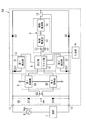
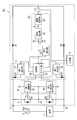
- FIG. 1 is a schematic circuit diagram illustrating a configuration of a light control device according to a first embodiment.
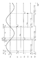
- 3 is a timing chart illustrating an operation of the light control device according to the first embodiment.
- 6 is a timing chart used for comparison between the light control device according to Embodiment 1 and a comparative example;
- FIG. 5 is a schematic circuit diagram illustrating a configuration of a light control device according to a first modification of the first embodiment.
- 10 is a schematic circuit diagram illustrating a configuration of a light control device according to a second modification of the first embodiment.
- FIG. 6 is a timing chart illustrating an operation of the light control device according to the second modification of the first embodiment.
- FIG. 5 is a schematic circuit diagram illustrating a configuration of a light control device according to a second embodiment.
- the light control device 1 of the present embodiment includes a pair of input terminals 11 and 12, a bidirectional switch 2, a phase detection unit 3, an input unit 4, a power supply unit 5, a control unit 6, and a switch drive unit. 9, diodes D1 and D2, and a stop unit 13 are provided.
- the pair of input terminals 11 and 12 are electrically connected between the load 7 that is lit when energized and the AC power supply 8.
- the bidirectional switch 2 is configured to switch between bidirectional current interruption / conduction between the pair of input terminals 11 and 12.
- the phase detector 3 detects the phase of the AC voltage Vac of the AC power supply 8.
- the input unit 4 receives a dimming level that specifies the magnitude of the light output of the load 7.
- the power supply unit 5 is electrically connected between the pair of input terminals 11 and 12, and generates a control power supply using power supplied from the AC power supply 8.
- the control unit 6 operates by receiving control power from the power supply unit 5. Based on the detection signal from the phase detection unit 3, the control unit 6 switches the bidirectional switch 2 so that the bidirectional switch 2 is turned off from the start point of the half cycle of the AC voltage Vac to the first time point when the first time elapses. 2 is controlled. The control unit 6 controls the bidirectional switch 2 so that the bidirectional switch 2 is turned on from the first time point to the second time point when the second time corresponding to the dimming level elapses. Further, the control unit 6 controls the bidirectional switch 2 so that the bidirectional switch 2 is turned off from the second time point to the end point of the half cycle.
- the expression “from time A” includes time A.
- “from the first time point” means to include the first time point.
- the expression “until time A” does not include time A but means immediately before time A.
- “up to the first time point” means not to include the first time point but to immediately before the first time point.
- the “input terminal” here does not have to be an entity as a component (terminal) for connecting an electric wire or the like, for example, a lead of an electronic component or a part of a conductor included in a circuit board. May be.
- the light control device 1 is a two-wire light control device, and is used in a state where it is electrically connected in series with a load 7 with respect to an AC power supply 8.
- the load 7 is lit when energized.
- the load 7 includes an LED element as a light source and a lighting circuit that lights the LED element.
- the AC power supply 8 is, for example, a single-phase 100 [V], 60 [Hz] commercial power supply.
- the light control device 1 is applicable to a wall switch or the like as an example.
- the bidirectional switch 2 includes, for example, two elements, a first switch element Q1 and a second switch element Q2, which are electrically connected in series between the input terminals 11 and 12.
- each of the switch elements Q1 and Q2 is a semiconductor switch element made of an enhancement type n-channel MOSFET (Metal-Oxide-Semiconductor Field Field Effect Transistor).
- the switch elements Q1 and Q2 are connected in reverse so-called between the input terminals 11 and 12. That is, the sources of the switch elements Q1 and Q2 are connected to each other.
- the drain of the switch element Q1 is connected to the input terminal 11, and the drain of the switch element Q2 is connected to the input terminal 12.
- the sources of both switch elements Q 1 and Q 2 are connected to the ground of the power supply unit 5.
- the ground of the power supply unit 5 serves as a reference potential for the internal circuit of the light control device 1.
- the bidirectional switch 2 can be switched between four states depending on the combination of ON and OFF of the switch elements Q1 and Q2.
- the four states include a bidirectional off state in which both switch elements Q1 and Q2 are both off, a bidirectional on state in which both switch elements Q1 and Q2 are both on, and only one of the switch elements Q1 and Q2 is on.
- the switch element Q1 when the switch element Q1 is on and the switch element Q2 is off, the first one-way on state in which current flows from the input terminal 11 toward the input terminal 12 is set. Further, when the switch element Q2 is on and the switch element Q1 is off, the second one-way on state in which current flows from the input terminal 12 toward the input terminal 11 is set. Therefore, when the AC voltage Vac is applied from the AC power supply 8 between the input terminals 11 and 12, the first one-way ON state is “in the positive polarity of the AC voltage Vac, that is, in the half cycle of the input terminal 11 being positive.
- the “forward ON state” and the second unidirectional ON state are “reverse ON state”.
- the second one-way on state is the “forward on state” and the first one-way on state is the “reverse on state”. It becomes.
- both the “bidirectional on state” and the “forward on state” are in the on state, and both the “bidirectional off state” and the “reverse on state” are in the off state. It is.
- the phase detector 3 detects the phase of the AC voltage Vac applied between the input terminals 11 and 12.
- the “phase” here includes the zero cross point of the AC voltage Vac and the polarity (positive polarity, negative polarity) of the AC voltage Vac.
- the phase detection unit 3 is configured to output a detection signal to the control unit 6 when the zero cross point of the AC voltage Vac is detected.
- the phase detection unit 3 includes a diode D31, a first detection unit 31, a diode D32, and a second detection unit 32.
- the first detection unit 31 is electrically connected to the input terminal 11 via the diode D31.
- the second detection unit 32 is electrically connected to the input terminal 12 via the diode D32.
- the first detector 31 detects a zero cross point when the AC voltage Vac shifts from a negative half cycle to a positive half cycle.
- the second detector 32 detects a zero cross point when the AC voltage Vac shifts from a positive half cycle to a negative half cycle.
- the first detection unit 31 detects that the voltage having the input terminal 11 as the positive electrode has shifted from a state below the specified value to a state above the specified value, it determines that it is a zero cross point.
- the second detection unit 32 detects that the voltage having the input terminal 12 as the positive electrode has shifted from a state less than the specified value to a state equal to or higher than the specified value, the second detecting unit 32 determines that it is a zero cross point.
- the specified value is a value (absolute value) set near 0 [V].
- the specified value of the first detector 31 is about a plus number [V]
- the specified value of the second detector 32 is about a minus number [V]. Therefore, the detection point of the zero cross point detected by the first detection unit 31 and the second detection unit 32 is slightly delayed from the zero cross point (0 [V]) in a strict sense.
- the input unit 4 receives a signal indicating the dimming level from the operation unit operated by the user, and outputs the signal to the control unit 6 as a dimming signal.
- the input unit 4 may or may not process the received signal when outputting the dimming signal.
- the dimming signal is a numerical value or the like that specifies the magnitude of the light output of the load 7 and may include an “OFF level” that turns off the load 7.
- the operation unit may be configured to output a signal indicating the dimming level to the input unit 4 in response to a user operation.
- the operation unit may be a variable resistor, a rotary switch, a touch panel, a remote controller, or a communication terminal such as a smartphone. is there.
- the control unit 6 controls the bidirectional switch 2 based on the detection signal from the phase detection unit 3 and the dimming signal from the input unit 4.
- the control unit 6 controls each of the switch elements Q1, Q2 separately. Specifically, the control unit 6 controls the switch element Q1 with the first control signal and controls the switch element Q2 with the second control signal.
- the control unit 6 includes, for example, a microcomputer as a main component.
- the microcomputer realizes a function as the control unit 6 by executing a program recorded in a memory of the microcomputer by a CPU (Central Processing Unit).
- the program may be recorded in advance in a memory of a microcomputer, may be provided by being recorded on a recording medium such as a memory card, or may be provided through an electric communication line.
- the program is a program for causing a computer (here, a microcomputer) to function as the control unit 6.
- the switch drive unit 9 includes a first drive unit 91 that drives the switch element Q1 (on / off control) and a second drive unit 92 that drives the switch element Q2 (on / off control).
- the first drive unit 91 receives the first control signal from the control unit 6 and applies a gate voltage to the switch element Q1. Accordingly, the first drive unit 91 performs on / off control of the switch element Q1.
- the second drive unit 92 receives the second control signal from the control unit 6 and applies a gate voltage to the switch element Q2. As a result, the second drive unit 92 performs on / off control of the switch element Q2.
- the first drive unit 91 generates a gate voltage with reference to the source potential of the switch element Q1. The same applies to the second drive unit 92.
- the power supply unit 5 includes a control power supply unit 51 that generates a control power supply, a drive power supply unit 52 that generates a drive power supply, and a capacitive element (capacitor) C1.
- the control power source is a power source for operation of the control unit 6.
- the drive power supply is a power supply for driving the switch drive unit 9.
- the capacitive element C ⁇ b> 1 is electrically connected to the output terminal of the control power supply unit 51 and is charged by the output current of the control power supply unit 51.
- the power supply unit 5 is electrically connected to the input terminal 11 via the diode D1, and is electrically connected to the input terminal 12 via the diode D2.
- the AC voltage Vac applied between the input terminals 11 and 12 is full-wave rectified by a diode bridge composed of a pair of diodes D1 and D2 and parasitic diodes of the switch elements Q1 and Q2. , Supplied to the power supply unit 5.
- the drive power supply unit 52 smoothes the full-wave rectified AC voltage Vac to generate a drive power supply.
- the drive power supply unit 52 supplies drive power to the switch drive unit 9 and the control power supply unit 51.
- the drive power supply is, for example, 10 [V].
- the control power supply 51 steps down the drive power supplied from the drive power supply 52 to generate a control power, and outputs the control power to the capacitive element C1.
- the control power supply is 3 [V], for example.
- the control power supply unit 51 may directly generate the control power supply from the full-wave rectified AC voltage Vac without using the drive power supply unit 52. That is, the power supply unit 5 generates a control power supply and a drive power supply using the power supplied from the AC power supply 8.
- the stop unit 13 stops the generation of the control power in the power source unit 5 during the stop period.
- the stopping unit 13 stops the generation of the control power supply in the power supply unit 5 by electrically cutting off the power supply unit 5 or controlling the semiconductor switch element included in the power supply unit 5.
- the stop unit 13 constitutes a series circuit with the power supply unit 5, and the series circuit of the stop unit 13 and the power supply unit 5 is electrically connected to the bidirectional switch 2 between the pair of input terminals 11 and 12. Connected in parallel.
- the stop period is a period that is set except at least the period in which the bidirectional switch 2 is in the bidirectional OFF state.
- the stop unit 13 is a switch electrically connected between the connection point of the pair of diodes D1 and D2 and the power supply unit 5 and is turned off in response to a cutoff signal from the control unit 6. Then, the power supply unit 5 is electrically disconnected from the input terminals 11 and 12.
- the light control device 1 of the present embodiment includes a mask unit 61.
- the mask unit 61 When receiving the detection signal from the phase detection unit 3, the mask unit 61 invalidates the detection signal over a certain length of mask time.
- the mask unit 61 is provided integrally with the control unit 6 as a function of the control unit 6. The details will be described in the column “(1.2.2) Dimming operation”, but the mask unit 61 disables the detection signal from the phase detection unit 3 during the mask time, thereby making the phase detection unit. 3 is less likely to be affected by the erroneous detection of the zero-cross point at 3.
- the mask unit 61 preferably invalidates the detection signal separately for each of the first detection unit 31 and the second detection unit 32.
- the lighting circuit of the load 7 reads the dimming level from the waveform of the AC voltage Vac phase-controlled by the dimmer 1 and changes the magnitude of the light output of the LED element.
- the lighting circuit has a current securing circuit such as a bleeder circuit as an example. Therefore, it is possible to pass a current through the load 7 even during a period when the bidirectional switch 2 of the light control device 1 is non-conductive.
- the AC power supply 8 when the AC power supply 8 is connected between the input terminals 11 and 12 via the load 7, the AC voltage Vac applied from the AC power supply 8 to the input terminals 11 and 12. Is rectified and supplied to the drive power supply unit 52.
- the drive power generated by the drive power supply unit 52 is supplied to the switch drive unit 9 and supplied to the control power supply unit 51.
- the control power generated by the control power supply unit 51 is supplied to the control unit 6, the control unit 6 is activated.
- the control unit 6 determines the frequency of the AC power supply 8 based on the detection signal of the phase detection unit 3. And the control part 6 sets parameters (for example, mask time and stop period mentioned later), such as various time, with reference to the numerical table previously memorize
- the dimming level input to the input unit 4 is “OFF level”
- the control unit 6 maintains the bidirectional switch 2 in the bidirectionally off state, so that the pair of input terminals 11, 12 is connected. Is maintained in a high impedance state. Thereby, the load 7 maintains a light extinction state.
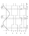
- FIG. 2 the AC voltage “Vac”, the first detection signal “ZC1”, the first mask process “MASK1”, the second detection signal “ZC2”, the second mask process “MASK2”, the first control signal “Sb1”, The second control signal “Sb2” and the cutoff signal “Ss1” are shown.
- the first detection signal ZC1 is a detection signal from the first detection unit 31
- the second detection signal ZC2 is a detection signal from the second detection unit 32.
- the first mask process MASK1 is a mask process (invalidation process) for the first detection signal ZC1 by the mask unit 61
- the second mask process MASK2 is a mask process for the second detection signal ZC2 by the mask unit 61.
- the first detection signal ZC1 is generated when the first detection signal ZC1 changes from the “H” level to the “L” level.
- the second detection signal ZC2 is generated when the second detection signal ZC2 changes from the “H” level to the “L” level. That is, the first detection signal ZC1 and the second detection signal ZC2 are signals that change from the “H” level to the “L” level when the zero cross point is detected.
- the dimmer 1 detects the zero cross point of the AC voltage Vac, which is a reference for phase control, by the phase detector 3.
- the first detection unit 31 outputs the first detection signal ZC1. Output.
- the control unit 6 turns the first control signal Sb1 and the second control signal Sb2 into “OFF” signals.
- the generation time point of the first detection signal ZC1 is set as a “detection point”, and a period from the start point (zero cross point) t0 of the half cycle to the detection point and a certain time (for example, 300 [ ⁇ s]) from the detection point.
- a total period until the elapses is defined as a first period T1.
- the control unit 6 controls the bidirectional switch 2 to the bidirectionally off state not only after the detection point but also during the period from the start point (zero cross point) t0 of the half cycle to the detection point.
- the time from the start point (zero cross point) t0 of the half cycle to the detection point is a fixed length of time, and therefore the first time (half cycle of the half cycle) in this embodiment.
- the time from the start point t0 to the first time point t1) is a fixed length of time.
- the control unit 6 turns the first control signal Sb1 and the second control signal Sb2 into “ON” signals.
- the second time point t2 is a time point when the second time corresponding to the dimming signal has elapsed from the first time point t1.
- the controller 6 changes the first control signal Sb1 to the “OFF” signal while maintaining the second control signal Sb2 at the “ON” signal.
- the switch elements Q1 and Q2 are both turned on, and the bidirectional switch 2 is in the bidirectionally on state. Therefore, in the second period T2, power is supplied from the AC power supply 8 to the load 7 via the bidirectional switch 2, and the load 7 is lit.
- the third time point t3 is a time that is a certain time (for example, 300 [ ⁇ s]) before the end point (zero cross point) t4 of the half cycle.
- the control unit 6 turns the first control signal Sb1 and the second control signal Sb2 into “OFF” signals.
- the third period T3 from the second time point t2 to the third time point t3 only the switch element Q1 of the switch elements Q1 and Q2 is turned off, and the bidirectional switch 2 is turned on in the reverse direction (that is, turned off). State). Therefore, in the third period T3, power from the AC power supply 8 to the load 7 is cut off.
- the operation of the light control device 1 when the AC voltage Vac is in the negative half cycle is basically the same as the positive half cycle.
- a period from the start point (zero cross point) t0 (t4) of the half cycle to the first time point t1 when the first time elapses is defined as a first period T1.
- the generation point of the second detection signal ZC2 is set as a “detection point”, a period from the start point (zero cross point) t0 (t4) of the half cycle to the detection point, and a certain time (for example, 300 [ ⁇ s] from the detection point. ]) Is the first period T1.
- the second time point t2 is a time point when the second time corresponding to the dimming signal has elapsed from the first time point t1, and the third time point t3 is more constant than the end point (zero cross point) t4 (t0) of the half cycle. This is the time before the time (for example, 300 [ ⁇ s]). That is, when the AC voltage Vac reaches the negative polarity specified value “ ⁇ Vzc”, the second detection unit 32 outputs the second detection signal ZC2. Upon receiving the second detection signal ZC2, the control unit 6 turns the first control signal Sb1 and the second control signal Sb2 into “OFF” signals. As a result, the bidirectional switch 2 is turned off in the first period T1. Then, at the first time point t1, the control unit 6 turns the first control signal Sb1 and the second control signal Sb2 into “ON” signals.
- the control unit 6 sets the second control signal Sb2 to the “OFF” signal while maintaining the first control signal Sb1 at the “ON” signal.
- the control unit 6 turns the first control signal Sb1 and the second control signal Sb2 into “OFF” signals.
- the control unit 6 turns the first control signal Sb1 and the second control signal Sb2 into “OFF” signals.
- the light control device 1 of the present embodiment alternately performs the positive half-cycle operation and the negative half-cycle operation described above for each half cycle of the AC voltage Vac, thereby dimming the load 7.
- the bidirectional switch is in the OFF state during the period from the start point (zero cross point) t0 of the half cycle to the first time point t1, and both during the period from the second time point t2 to the end point (zero cross point) t4 of the half cycle.
- the direction switch is in the off state. Therefore, when focusing on two consecutive half cycles, the bidirectional switch is from the second time point t2 of the first half cycle to the first time point t1 of the next half cycle (ie, the second half cycle). Turns off.
- the interval between the input terminals 11 and 12 is half a cycle.
- the conduction time will be defined according to the dimming level. That is, when the light output of the load 7 is reduced, the second time is defined as short, and when the light output of the load 7 is increased, the second time is defined as long. Therefore, the magnitude of the light output of the load 7 can be changed according to the dimming level input to the input unit 4. Further, before and after the zero cross point of the AC voltage Vac, there are periods (first period T1 and fourth period T4) in which the bidirectional switch 2 is in the bidirectional OFF state.
- the power supply from the AC power supply 8 to the power supply unit 5 can be secured using the period.
- priority is given to securing the first period T1 and the fourth period T4, and the light output is not performed for the second period T2. You may make it control in a period shorter than the length to maximize.
- the light control apparatus 1 of this embodiment is provided with the mask part 61, and after receiving the zero cross point detection signal, the mask process which invalidates the subsequent zero cross point detection signal over a fixed length of mask time. Is going. That is, after receiving the first detection signal ZC1 from the first detection unit 31, the mask unit 61 turns on the first mask process MASK1 and invalidates the first detection signal ZC1 until the mask time elapses. . Similarly, after receiving the second detection signal ZC2 from the second detection unit 32, the mask unit 61 turns on the second mask processing MASK2 and disables the second detection signal ZC2 until the mask time elapses. To do.
- the length of the mask time is set on the basis of the half cycle of the AC voltage Vac.
- the mask time is a time slightly shorter than twice the half cycle (that is, one cycle).
- the first detection signal ZC1 and the second detection signal ZC2 in the invalidated period are represented by broken lines.
- the light control device 1 of this embodiment controls the stop part 13 with the interruption
- the stop unit 13 stops the generation of the control power supply in the power supply unit 5 by electrically shutting off the power supply unit 5 or controlling the semiconductor switch element included in the power supply unit 5. Yes. That is, the control unit 6 electrically disconnects the power supply unit 5 from the input terminals 11 and 12 by setting the cutoff signal Ss1 to the “OFF” signal and turning off the stop unit 13 during the stop period.
- the stop period is a period set excluding at least a period in which the bidirectional switch 2 is in the bidirectional off state (first period T1, fourth period T4).
- the stop period is set within the second period T2 in which the bidirectional switch 2 is in the bidirectional on state and the third period T3 in which the bidirectional switch 2 is in the one-way on state (reverse direction on state).
- the stop period is set so that the time point set between the first time point t1 and the second time point t2 is the start point and the third time point t3 is the end point. That is, the stop period is set within a period during which power may be supplied from the AC power supply 8 to the load 7.
- the light control device 1 can maintain the impedance between the input terminals 11 and 12 high by the part which disconnected the power supply part 5 from the input terminals 11 and 12 in the stop period. That is, the light control device 1 supplies power from the AC power supply 8 to the power supply unit 5 while the bidirectional switch 2 is in the bidirectional OFF state, and does not supply power to the power supply unit 5 (stop period).
- the impedance between the input terminals 11 and 12 can be kept high. For example, when the impedance between the input terminals 11 and 12 is maintained high during the third period T3 in which the bidirectional switch 2 is in the reverse ON state, power is supplied to the load 7 due to leakage current. Can be prevented. As a result, the magnitude of the light output of the load 7 can be changed following a minute change in the light control level, and the response of the load 7 is improved.
- the light control device 1 includes the bidirectional switch 2, the phase detection unit 3, the power supply unit 5, and the control. Part 6.
- the bidirectional switch 2 is connected in series with the load 7 with respect to the AC power supply 8 and controls the phase of the AC voltage Vac supplied to the load 7.
- the phase detector 3 detects the phase of the AC voltage Vac of the AC power supply 8.
- the power supply unit 5 includes a capacitive element C1 that is connected in parallel with the bidirectional switch 2, performs a conversion operation for converting the AC power supply 8 into a predetermined control power supply, and stores the control power supply.
- the control unit 6 is supplied with control power from the power supply unit 5 through the capacitive element C1, and based on the phase detected by the phase detection unit 3, the half-cycle period of the AC voltage Vac is set to the first period T1 and the second period.
- Period T2 third period T3, and fourth period T4.
- the control unit 6 controls the bidirectional switch 2 to be non-conductive, cuts off the power supply to the load 7, and causes the power source unit 5 to perform a conversion operation.
- the control unit 6 controls conduction of the bidirectional switch 2 to supply power to the load 7 and causes the power supply unit 5 to stop the conversion operation.
- the control unit 6 controls the bidirectional switch 2 to be non-conductive and cuts off the power supply to the load 7.
- Non-conducting control here means control to turn off the bidirectional switch 2.
- Conductivity control means control for turning on the bidirectional switch 2.
- conversion operation means an operation of converting the AC power supply 8 to a predetermined control power supply in the power supply unit 5, that is, an operation of generating a control power supply with power supplied from the AC power supply 8.
- the light control device 1 may further include a stop unit 13 that switches execution / stop of the conversion operation of the power supply unit 5.
- the control unit 6 controls the non-conduction of the bidirectional switch 2 to cut off the power supply to the load 7, and the stop unit 13 The conversion operation may be stopped.
- the light control device of the comparative example alternately “ONs” the first control signal Sa1 and the second control signal Sa2 in the same cycle as the AC voltage Vac.
- the bidirectional switch 2 becomes conductive during the period when the switch element on the high potential side of the AC voltage Vac is on among the switch elements Q1 and Q2. That is, in the comparative example, in FIG. 3, so-called reverse phase control is realized in which the pair of input terminals 11 and 12 are conductive in a period Ta1 from the zero cross point of the AC voltage Vac to the middle of the half cycle. Therefore, the conduction time of the bidirectional switch 2 can be adjusted by adjusting the phase difference between the first control signal Sa1 and the second control signal Sa2 and the AC voltage Vac.
- the bidirectional switch 2 is turned on in one direction (forward direction turned on), whereby the pair of input terminals 11 and 12 are electrically connected.
- the bidirectional switch 2 is When the bidirectional on state is established, the pair of input terminals 11 and 12 are electrically connected.
- the bidirectional switch 2 is in the bidirectional on state when the pair of input terminals 11 and 12 are in conduction, and thus the bidirectional switch 2 is in the unidirectional on state. Compared with the comparative example, the conduction loss in the bidirectional switch 2 can be reduced.
- the bidirectional switch 2 is in a bidirectional OFF state (first period T1, fourth period T4). Is different from the comparative example in that such a period does not exist.
- the dimming device 1 of the present embodiment turns off the bidirectional switch 2 bidirectionally in the period from the start point (zero cross point) t0 of the half cycle to the first time point t1 (first period T1). Since this is the state, this period can be used for power supply to the power supply unit 5.
- the light control device 1 of the present embodiment basically employs the antiphase control, but has a period (first period T1) in which the bidirectional switch 2 is non-conductive in the first half of the half cycle of the AC voltage Vac. By providing, the opportunity of the electric power supply from AC power supply 8 to the power supply part 5 can be ensured in the first half part of a half cycle. Therefore, the light control device 1 of the present embodiment can maintain power supply from the power supply unit 5 to the control unit 6 corresponding to more types of loads 7 as compared with the comparative example.
- the dimmer 1 also turns off the bidirectional switch 2 during the period from the third time point t3 to the end point t4 of the half cycle (fourth period T4). Can be used for power supply.
- the light control device 1 provides a power supply from the AC power supply 8 to the power supply unit 5 by providing a period (fourth period T4) in which the bidirectional switch 2 is non-conductive also in the latter half of the half cycle. Opportunities can be secured in the second half of the half cycle.
- the dimmer control method includes a pair of input terminals 11 and 12 in the period from the middle of the half cycle of the AC voltage Vac to the zero cross point.
- a positive phase control method leading edge method
- the anti-phase control method power supply is started from the zero cross point to the load 7 including the LED element as the light source, so that the current waveform distortion at the start of power supply can be suppressed to a low level.
- the light control device 1 of the present embodiment basically employs the antiphase control method, but provides an opportunity for power supply from the AC power supply 8 to the power supply unit 5 in the first half of the half cycle of the AC voltage Vac. .
- the current waveform distortion may be larger than in the antiphase control method as in the comparative example.
- the absolute value of the AC voltage Vac at the first time point t1 is not so large, the influence of the current waveform distortion is so small that it can be ignored.
- there is an advantage that a control power source necessary for the operation of the control unit 6 can be reliably ensured and can be stably operated.
- the dimming device 1 of the present embodiment sets the bidirectional switch 2 in the reverse direction ON state during the period from the second time point t2 to the third time point t3 (third time period T3). 3 false detection can be reduced. That is, depending on the load 7, the absolute value of the voltage across the load 7 exceeds the absolute value of the AC voltage Vac, and as a result, a voltage having a polarity opposite to that of the AC voltage Vac (hereinafter referred to as “reverse polarity voltage”) is a pair. It may be applied to the input terminals 11 and 12.
- a reverse polarity voltage is likely to occur.
- the phase detector 3 may erroneously detect the zero cross point at a place other than the zero cross point of the AC voltage Vac.
- a load 7 in which a reverse polarity voltage is generated or not generated depending on the dimming level With such a load 7, when the dimming level changes, the zero cross point changes suddenly.
- the bidirectional switch 2 since the bidirectional switch 2 is turned on in the reverse direction, the generation of such a reverse polarity voltage is suppressed, so that the erroneous detection of the phase detection unit 3 due to the reverse polarity voltage is prevented. Can be reduced.
- the pair of input terminals 11 and 12 are non-conductive. Thus, this period can be used for power supply to the power supply unit 5.
- the light control device 1 can prevent abnormal operation such as blinking of the load 7 or flickering by maintaining the power supply from the power supply unit 5 to the control unit 6.
- the bidirectional switch 2 in the present embodiment, it is possible to control to the “forward ON state” instead of the “bidirectional ON state”, and conversely, instead of the “forward ON state”, “ It is also possible to control to “bidirectional on state”. Further, it is possible to control the “reverse direction ON state” instead of the “bidirectional off state”, and it is possible to control the “bidirectional off state” instead of the “reverse direction ON state”. That is, it is sufficient that the bidirectional switch 2 does not change the on state or the off state.
- the bidirectional switch 2 includes a bidirectional off state that interrupts bidirectional current, a bidirectional on state that allows bidirectional current to pass between the input terminals 11 and 12, and a unidirectional relationship. It is preferable that the unidirectional ON state that allows the current to pass through be switched.
- the control unit 6 operates the bidirectional switch so that the bidirectional switch 2 is reversely turned on from the second time point t2 to the third time point t3 between the second time point t2 and the end point of the half cycle. 2 is preferably controlled.
- the “reverse direction ON state” is a one-way ON state in which the bidirectional switch 2 flows current from the low potential side input terminal of the AC power supply 8 to the high potential side input terminal of the input terminals 11 and 12. . According to this configuration, since the generation of the reverse polarity voltage is suppressed from the second time point t2 to the third time point t3, it is possible to reduce erroneous detection of the phase detection unit 3 due to the reverse polarity voltage.
- the power supply unit 5 preferably has a capacitive element C1. According to this configuration, the power supply unit 5 can store the power supplied from the AC power supply 8 in the capacitive element C1 during a period in which the input terminals 11 and 12 are not conducting. Therefore, the power supply unit 5 can secure a control power supply for the control unit 6 even during a period in which the input terminals 11 and 12 are conductive. However, it is not essential for the light control device 1 that the power supply unit 5 includes the capacitive element C1, and the capacitive element C1 may be omitted as appropriate.
- the first time is preferably a fixed time.
- the control unit 6 bidirectionally switches the bidirectional switch 2 during a period (first period T1) from the half-cycle start point (zero cross point) t0 until the first length of time has elapsed. What is necessary is just to control to an OFF state. Therefore, the process of the control unit 6 is simplified compared to the case where the length of the first time changes.
- the length of the first time is different between the first period T1 in the positive half-cycle and the first period T1 in the negative half-cycle. Is also possible.
- the phase detector 3 is configured to output a detection signal when the zero cross point of the AC voltage Vac is detected.
- the light control device 1 further includes a mask unit 61 that invalidates the detection signal over a predetermined length of mask time when the detection signal is received from the phase detection unit 3.
- the mask part 61 in this embodiment is not an essential component for the light control device 1, and the mask part 61 may be omitted as appropriate.
- the light control device 1 further includes a stop unit 13 that stops the generation of the control power supply in the power supply unit 5 during the stop period.
- the stop period is a period set except at least a period in which the bidirectional switch 2 is off.
- the stop unit 13 in the present embodiment is not an essential component of the light control device 1, and the stop unit 13 may be omitted as appropriate.
- the bidirectional switch 2 preferably includes switch elements Q1, Q2 electrically connected in series between the pair of input terminals 11, 12.
- the bidirectional switch 2A includes a switching element Q3 having a double gate structure.
- the switch element Q3 is a semiconductor element having a double gate (dual gate) structure using a wide band gap semiconductor material such as GaN (gallium nitride).
- the bidirectional switch 2A includes a pair of diodes D3 and D4 connected between the input terminals 11 and 12 in a so-called reverse series.
- the cathode of the diode D3 is connected to the input terminal 11, and the cathode of the diode D4 is connected to the input terminal 12.
- the anodes of both the diodes D3 and D4 are electrically connected to the ground of the power supply unit 5.
- the pair of diodes D3 and D4 form a diode bridge together with the pair of diodes D1 and D2.
- the bidirectional switch 2A can further reduce the conduction loss compared to the bidirectional switch 2.
- the control unit 6B has a zero-cross point of the AC voltage Vac that is a half cycle or more ahead based on a single zero-cross point detection signal. It differs from the light control apparatus 1 of Embodiment 1 by the point comprised so that may be estimated.
- the circuit configuration of the dimmer 1B is the same as that of the dimmer 1 of the first embodiment.
- the same configurations as those of the first embodiment are denoted by common reference numerals, and description thereof will be omitted as appropriate.
- phase detector 3 is configured to output a detection signal when it detects the zero-cross point of the AC voltage Vac is the same as in the first embodiment.
- the control unit 6B estimates a zero-cross point ahead of a half cycle or more of the AC voltage Vac as a virtual zero-cross point every time a detection signal is received from the phase detection unit 3 based on the frequency of the AC voltage Vac.
- a virtual signal is generated at the virtual zero cross point timing. Specifically, as illustrated in FIG. 6, the control unit 6B determines that the first virtual signal Si1 when the standby time Tzc corresponding to one cycle of the AC voltage Vac has elapsed from the time when the first detection signal ZC1 is received. Is generated.
- the control unit 6B generates the second virtual signal Si2 when a standby time Tzc corresponding to one cycle of the AC voltage Vac has elapsed since the time when the second detection signal ZC2 was received.
- the standby time Tzc is set slightly longer than one cycle of the AC voltage Vac so that the first virtual signal Si1 is not generated prior to the next first detection signal ZC1.
- the standby time Tzc is set slightly longer than one cycle of the AC voltage Vac so that the second virtual signal Si2 is not generated prior to the next second detection signal ZC2.
- the control unit 6B uses the logical sum of the first detection signal ZC1 and the first virtual signal Si1 as a trigger signal for determining the control timing of the bidirectional switch 2. Similarly, the control unit 6B uses a logical sum of the second detection signal ZC2 and the second virtual signal Si2 as a trigger signal for determining the control timing of the bidirectional switch 2. Therefore, even when the phase detection unit 3 fails to detect the zero cross point, the control unit 6B uses the virtual signal generated at the virtual zero cross point as a trigger signal instead of the detection signal from the phase detection unit 3, and The control timing of the switch 2 can be determined.
- the control unit 6B may be configured to estimate the virtual zero cross point twice or more with respect to a single zero cross point detection signal. In this case, the control unit 6B generates a virtual signal every time the standby time Tzc elapses from the time when the detection signal is received.
- the first standby time Tzc is a little longer than one cycle of the AC voltage Vac
- the second and subsequent standby times Tzc are of the same length as one cycle of the AC voltage Vac. The length may be changed.
- the standby time Tzc for generating the virtual signal may be set on the basis of the half cycle of the AC voltage Vac, in addition to one cycle, half cycle, three times the half cycle (that is, 1.5 cycle), half It may be set based on four times the period (that is, two periods) or more.
- the control unit 6B When the standby time Tzc is set based on an odd multiple of a half cycle, the control unit 6B generates the second virtual signal Si2 when the standby time Tzc has elapsed based on the first detection signal ZC1. In this case, the control unit 6B generates the first virtual signal Si1 when the standby time Tzc has elapsed based on the second detection signal ZC2. Therefore, the control unit 6B may be configured to generate the first virtual signal Si1 and the second virtual signal Si2 from only one of the first detection signal ZC1 and the second detection signal ZC2.
- control unit 6B performs stable antiphase control in synchronization with the cycle of the AC voltage Vac.
- the light control devices according to the first embodiment and the first and second modifications described above are not limited to the load 7 using an LED element as a light source, but are equipped with a capacitor input type circuit, which has a high impedance and is lit with a small current. Applicable.
- An example of this type of light source is an organic EL (Electroluminescence) element.
- the light control device can be applied to the load 7 of various light sources such as a discharge lamp.
- the switch drive unit 9 is not an essential component of the light control device 1 and may be omitted as appropriate.
- the control unit 6 drives the bidirectional switch 2 directly.
- the mask unit 61 may be configured to invalidate the detection signal over a certain length of mask time, and is not limited to the configuration provided integrally with the control unit 6. That is, the mask unit 61 may be provided integrally with the phase detection unit 3, for example, and in this case, the detection signal is invalidated by the mask unit 61 stopping the operation of the phase detection unit 3 over the mask period. Can be. Further, the mask unit 61 may be provided separately from the control unit 6 and the phase detection unit 3.
- the mask time may be a time set in advance with reference to the half cycle of the AC voltage Vac, and is slightly shorter than twice the half cycle (that is, one cycle) as illustrated in the first embodiment. Not exclusively.
- the mask time may be a time slightly shorter than a half cycle or a time slightly shorter than three times a half cycle (that is, 1.5 cycles). Further, the mask time may be set on the basis of four times (that is, two cycles) or more of a half cycle.
- each of the switch elements Q1 and Q2 constituting the bidirectional switch 2 is not limited to an enhancement type n-channel MOSFET, but may be, for example, an IGBT (Insulated Gate Bipolar Transistor) or the like.
- the rectifying element (diode) for realizing the unidirectional ON state is not limited to the parasitic diode of the switching elements Q1 and Q2, but may be an external diode as in the first modification. Good.
- the diode may be incorporated in the same package as each of the switch elements Q1, Q2.
- the first time may be a certain length of time, and the length can be set as appropriate.
- the delay time is 300 [ ⁇ s. However, it is appropriately set within the range of 0 [ ⁇ s] to 500 [ ⁇ s].
- the third time point t3 only needs to be before the end point (zero cross point) t4 of the half cycle, and the length from the third time point t3 to the end point t4 of the half cycle can be appropriately set.
- the specified time is not limited to 300 [ ⁇ s], but ranges from 100 [ ⁇ s] to 500 [ ⁇ s]. Is set as appropriate.
- the stop period in which the stop unit 13 electrically disconnects between the pair of input terminals 11 and 12 and the power supply unit 5 is at least a period in which the bidirectional switch 2 is in the bidirectional off state (first period T1, Any period may be set except for the fourth period T4). Therefore, the stop period is not limited to a period starting from the time point between the first time point t1 and the second time point t2 and ending at the third time point t3 as in the first embodiment. It may be one time point t1, and the end point of the stop period may be before the third time point t3.
- the stop part 13 should just be the structure which stops the production
- the stop unit 13 is configured to increase the input impedance of the power supply unit 5 by stopping the output of the power supply unit 5 (output of the control power supply) and stop the generation of the control power supply in the power supply unit 5. Good.
- the diodes D1 and D2 in the present embodiment are not essential to the light control device 1, and the diodes D1 and D2 may be omitted as appropriate.
- the light control device 1 ⁇ / b> C of the present embodiment further includes a voltage detection unit 53 that detects the voltage of the control power supply (the voltage of the capacitive element C ⁇ b> 1). Is different.
- the same configurations as those of the first embodiment are denoted by common reference numerals, and description thereof will be omitted as appropriate.
- the first time is not a fixed length of time, and the voltage (voltage of the capacitive element C1) detected by the voltage detection unit 53 from the start point (zero cross point) t0 of the half cycle of the AC voltage Vac is predetermined. This is the time to reach the threshold. That is, the first time in the present embodiment is not a fixed-length time, but a variable-length time that changes according to the detection value of the voltage detection unit 53.
- the voltage detection unit 53 is provided in the power supply unit 5C.
- the voltage detection unit 53 detects the voltage across the capacitive element C1 of the power supply unit 5C and outputs the detection value to the control unit 6C.
- the control unit 6C compares the detection value of the voltage detection unit 53 with a predetermined threshold value, and the first time has elapsed when the detection value has reached the threshold value ( That is, it is determined that the first time point t1).
- the threshold value is the voltage across the capacitive element C1 when the capacitive element C1 is charged to such an extent that the operation of the control unit 6 can be ensured at least up to the end point (zero cross point) t4 of the half cycle of the AC voltage Vac.
- the light control device 1C of the present embodiment further includes the voltage detection unit 53 that detects the voltage of the control power supply, and the first time is a voltage detected by the voltage detection unit 53 from the start point of the half cycle. Is the time to reach a predetermined threshold.
- the control unit 6 sets the bidirectional switch 2 to the bidirectional on state when the capacitive element C1 is charged to such an extent that a control power source necessary for the operation of the control unit 6 can be secured. Can do. Therefore, the light control device 1C according to the present embodiment reliably secures a control power supply necessary for the operation of the control unit 6 and connects between the input terminals 11 and 12 from the start point (zero cross point) t0 of the half cycle of the AC voltage Vac. The time until conduction can be shortened as much as possible.
- the capacitive element C1 may be a parasitic capacitance, and in that case, there is no separate capacitive element.
- alternating current is generated around the first point (zero cross point) t0 of the half cycle of the alternating voltage Vac (first period T1, fourth period T4).
- first period T1, fourth period T4 fourth period T4
- the power supply from the AC power source 8 to the power source unit 5 may be ensured for a certain period of time. Further, the power supply from the AC power supply 8 to the power supply unit 5 may be ensured for a certain time only before the start point (zero cross point) t0 of the half cycle of the AC voltage Vac (fourth period T4). Even in this case, since the first period T1 or the fourth period T4 is set with priority given to securing the power supply from the AC power supply 8 to the power supply unit 5, the dimming level input to the input unit 4 is set. Accordingly, the second period T2 for supplying power to the load 7 may not be set. For example, this is a case where the user operates the operation unit to maximize the light output of the load 7.
- the control unit 6 can be stably operated while suppressing current waveform distortion by setting the above-mentioned fixed time so that the power supply from the AC power supply 8 to the power supply unit 5 can be sufficiently performed.
Landscapes
- Circuit Arrangement For Electric Light Sources In General (AREA)
Priority Applications (9)
| Application Number | Priority Date | Filing Date | Title |
|---|---|---|---|
| US15/580,027 US10306732B2 (en) | 2015-06-08 | 2016-05-30 | Dimmer |
| JP2017513826A JP6218101B2 (ja) | 2015-06-08 | 2016-05-30 | 調光装置 |
| ES16807085T ES2849803T3 (es) | 2015-06-08 | 2016-05-30 | Atenuador de luz |
| CN201680033598.1A CN107683631B (zh) | 2015-06-08 | 2016-05-30 | 调光装置 |
| KR1020177035312A KR102075896B1 (ko) | 2015-06-08 | 2016-05-30 | 조광 장치 |
| EP16807085.2A EP3307026B1 (en) | 2015-06-08 | 2016-05-30 | Dimmer |
| CN202110518102.2A CN113271699B (zh) | 2015-06-08 | 2016-05-30 | 调光装置 |
| US16/194,350 US10616975B2 (en) | 2015-06-08 | 2018-11-18 | Dimmer |
| US16/818,278 US10966302B2 (en) | 2015-06-08 | 2020-03-13 | Dimmer |
Applications Claiming Priority (2)
| Application Number | Priority Date | Filing Date | Title |
|---|---|---|---|
| JP2015116179 | 2015-06-08 | ||
| JP2015-116179 | 2015-06-08 |
Related Child Applications (2)
| Application Number | Title | Priority Date | Filing Date |
|---|---|---|---|
| US15/580,027 A-371-Of-International US10306732B2 (en) | 2015-06-08 | 2016-05-30 | Dimmer |
| US16/194,350 Continuation US10616975B2 (en) | 2015-06-08 | 2018-11-18 | Dimmer |
Publications (1)
| Publication Number | Publication Date |
|---|---|
| WO2016199368A1 true WO2016199368A1 (ja) | 2016-12-15 |
Family
ID=57503784
Family Applications (1)
| Application Number | Title | Priority Date | Filing Date |
|---|---|---|---|
| PCT/JP2016/002605 Ceased WO2016199368A1 (ja) | 2015-06-08 | 2016-05-30 | 調光装置 |
Country Status (8)
| Country | Link |
|---|---|
| US (3) | US10306732B2 (https=) |
| EP (1) | EP3307026B1 (https=) |
| JP (6) | JP6218101B2 (https=) |
| KR (1) | KR102075896B1 (https=) |
| CN (2) | CN107683631B (https=) |
| ES (1) | ES2849803T3 (https=) |
| TW (1) | TWI620466B (https=) |
| WO (1) | WO2016199368A1 (https=) |
Cited By (5)
| Publication number | Priority date | Publication date | Assignee | Title |
|---|---|---|---|---|
| CN108243545A (zh) * | 2016-12-27 | 2018-07-03 | 松下知识产权经营株式会社 | 负载控制装置 |
| CN108243538A (zh) * | 2016-12-27 | 2018-07-03 | 松下知识产权经营株式会社 | 负载控制装置 |
| WO2020022249A1 (ja) * | 2018-07-27 | 2020-01-30 | パナソニックIpマネジメント株式会社 | 負荷制御システム |
| JP2020087892A (ja) * | 2018-11-30 | 2020-06-04 | パナソニックIpマネジメント株式会社 | 負荷制御装置 |
| JP2021052023A (ja) * | 2021-01-07 | 2021-04-01 | パナソニックIpマネジメント株式会社 | 負荷制御装置 |
Families Citing this family (20)
| Publication number | Priority date | Publication date | Assignee | Title |
|---|---|---|---|---|
| CN103024994B (zh) * | 2012-11-12 | 2016-06-01 | 昂宝电子(上海)有限公司 | 使用triac调光器的调光控制系统和方法 |
| CN103957634B (zh) | 2014-04-25 | 2017-07-07 | 广州昂宝电子有限公司 | 照明系统及其控制方法 |
| KR102075896B1 (ko) | 2015-06-08 | 2020-02-11 | 파나소닉 아이피 매니지먼트 가부시키가이샤 | 조광 장치 |
| JP6481943B2 (ja) | 2015-09-10 | 2019-03-13 | パナソニックIpマネジメント株式会社 | 調光装置 |
| JP6867780B2 (ja) * | 2016-10-28 | 2021-05-12 | 矢崎総業株式会社 | 半導体スイッチ制御装置 |
| CN107645804A (zh) | 2017-07-10 | 2018-01-30 | 昂宝电子(上海)有限公司 | 用于led开关控制的系统 |
| CN107682953A (zh) | 2017-09-14 | 2018-02-09 | 昂宝电子(上海)有限公司 | Led照明系统及其控制方法 |
| CN107995730B (zh) | 2017-11-30 | 2020-01-07 | 昂宝电子(上海)有限公司 | 用于与triac调光器有关的基于阶段的控制的系统和方法 |
| CN108200685B (zh) | 2017-12-28 | 2020-01-07 | 昂宝电子(上海)有限公司 | 用于可控硅开关控制的led照明系统 |
| CN109922564B (zh) | 2019-02-19 | 2023-08-29 | 昂宝电子(上海)有限公司 | 用于triac驱动的电压转换系统和方法 |
| CN110493913B (zh) | 2019-08-06 | 2022-02-01 | 昂宝电子(上海)有限公司 | 用于可控硅调光的led照明系统的控制系统和方法 |
| CN110831295B (zh) | 2019-11-20 | 2022-02-25 | 昂宝电子(上海)有限公司 | 用于可调光led照明系统的调光控制方法和系统 |
| CN110831289B (zh) | 2019-12-19 | 2022-02-15 | 昂宝电子(上海)有限公司 | Led驱动电路及其操作方法和供电控制模块 |
| CN111031635B (zh) | 2019-12-27 | 2021-11-30 | 昂宝电子(上海)有限公司 | 用于led照明系统的调光系统及方法 |
| TWI726606B (zh) | 2020-02-07 | 2021-05-01 | 群光電能科技股份有限公司 | 負載識別系統 |
| CN111432526B (zh) | 2020-04-13 | 2023-02-21 | 昂宝电子(上海)有限公司 | 用于led照明系统的功率因子优化的控制系统和方法 |
| CN112165752B (zh) * | 2020-09-08 | 2023-04-07 | 杭州涂鸦信息技术有限公司 | 一种单火调光双控开关异常零点信号的调节方法及系统 |
| FR3114457B1 (fr) * | 2020-09-18 | 2022-09-09 | Commissariat Energie Atomique | Commande de deux interrupteurs en série |
| JP7345225B1 (ja) * | 2023-05-22 | 2023-09-15 | 株式会社イー・ティー・エル | 調光装置、および照明コントロールシステム |
| CN119300204A (zh) * | 2023-07-10 | 2025-01-10 | 施耐德电气工业公司 | 用于调光装置的控制电路、方法及调光装置 |
Citations (2)
| Publication number | Priority date | Publication date | Assignee | Title |
|---|---|---|---|---|
| JP2011050149A (ja) * | 2009-08-26 | 2011-03-10 | Panasonic Electric Works Co Ltd | 負荷制御装置 |
| JP2013251189A (ja) * | 2012-06-01 | 2013-12-12 | Jimbo Electric Co Ltd | 調光装置 |
Family Cites Families (50)
| Publication number | Priority date | Publication date | Assignee | Title |
|---|---|---|---|---|
| JP3630019B2 (ja) * | 1999-06-25 | 2005-03-16 | 松下電工株式会社 | 2線式配線器具 |
| US6266260B1 (en) * | 1999-09-03 | 2001-07-24 | Powerware Corporation | Inverter having center switch and uninterruptible power supply implementing same |
| DE10315554B3 (de) | 2003-04-05 | 2004-08-19 | Theben Ag | Dimmer Booster |
| WO2004110110A1 (ja) * | 2003-06-04 | 2004-12-16 | Matsushita Electric Industrial Co., Ltd. | 放電ランプ点灯装置 |
| US7242150B2 (en) | 2005-05-12 | 2007-07-10 | Lutron Electronics Co., Inc. | Dimmer having a power supply monitoring circuit |
| US7190124B2 (en) * | 2005-05-16 | 2007-03-13 | Lutron Electronics Co., Inc. | Two-wire dimmer with power supply and load protection circuit in the event of switch failure |
| US7847440B2 (en) * | 2005-06-06 | 2010-12-07 | Lutron Electronics Co., Inc. | Load control device for use with lighting circuits having three-way switches |
| AU2006265902C1 (en) * | 2005-06-30 | 2010-02-11 | Lutron Electronics Co., Inc. | Dimmer having a microprocessor-controlled power supply |
| US7602157B2 (en) * | 2005-12-28 | 2009-10-13 | Flyback Energy, Inc. | Supply architecture for inductive loads |
| US7566995B2 (en) * | 2006-06-20 | 2009-07-28 | Lutron Electronics Co., Inc. | Touch screen having a uniform actuation force and a maximum active area |
| JP2008278670A (ja) * | 2007-05-01 | 2008-11-13 | Funai Electric Co Ltd | 他励式インバータ回路及び液晶テレビジョン |
| US8129976B2 (en) * | 2007-08-09 | 2012-03-06 | Lutron Electronics Co., Inc. | Load control device having a gate current sensing circuit |
| US8339062B2 (en) | 2008-05-15 | 2012-12-25 | Marko Cencur | Method for dimming non-linear loads using an AC phase control scheme and a universal dimmer using the method |
| US8193730B2 (en) * | 2008-06-12 | 2012-06-05 | 3M Innovative Properties Company | Dimmer and illumination apparatus with amplitude ordered illumination of multiple strings of multiple color light emitting devices |
| JP5438004B2 (ja) * | 2008-07-24 | 2014-03-12 | パナソニック株式会社 | 電力変換装置 |
| JP5294903B2 (ja) | 2008-08-21 | 2013-09-18 | パナソニック株式会社 | 負荷制御装置及びそれを備えた負荷制御システム |
| KR101001241B1 (ko) * | 2008-09-05 | 2010-12-17 | 서울반도체 주식회사 | 교류 led 조광장치 및 그에 의한 조광방법 |
| MY164929A (en) | 2008-12-22 | 2018-02-15 | Panasonic Ip Man Co Ltd | Load control device |
| US8451116B2 (en) * | 2009-03-27 | 2013-05-28 | Lutron Electronics Co., Inc. | Wireless battery-powered daylight sensor |
| CN102576233B (zh) * | 2009-08-26 | 2014-11-26 | 松下电器产业株式会社 | 负载控制装置 |
| JP5362484B2 (ja) * | 2009-08-26 | 2013-12-11 | パナソニック株式会社 | 負荷制御装置 |
| US8466628B2 (en) * | 2009-10-07 | 2013-06-18 | Lutron Electronics Co., Inc. | Closed-loop load control circuit having a wide output range |
| MX2012005844A (es) * | 2009-11-20 | 2012-09-28 | Lutron Electronics Co | Circuito de carga controlable para su uso con un dispositivo de control de carga. |
| US8664881B2 (en) * | 2009-11-25 | 2014-03-04 | Lutron Electronics Co., Inc. | Two-wire dimmer switch for low-power loads |
| JP5501851B2 (ja) * | 2010-05-12 | 2014-05-28 | Tone株式会社 | 位相制御装置 |
| JP5785611B2 (ja) * | 2010-05-17 | 2015-09-30 | コーニンクレッカ フィリップス エヌ ヴェ | 不適当な調光器動作を検出し修正するための方法及び装置 |
| CN102751881B (zh) * | 2011-04-02 | 2014-12-10 | 英飞特电子(杭州)股份有限公司 | 一种两线调光器的辅助电源电路 |
| KR101264175B1 (ko) * | 2011-04-29 | 2013-05-14 | 한국전기연구원 | 위상제어 조광기 |
| WO2012170856A1 (en) * | 2011-06-10 | 2012-12-13 | Lutron Electronics Co., Inc. | Method and apparatus for adjusting an ambient light threshold |
| US9386666B2 (en) * | 2011-06-30 | 2016-07-05 | Lutron Electronics Co., Inc. | Method of optically transmitting digital information from a smart phone to a control device |
| JP5342626B2 (ja) * | 2011-09-27 | 2013-11-13 | シャープ株式会社 | Led駆動回路及びこれを用いたled照明灯具 |
| CN102386779B (zh) * | 2011-12-06 | 2013-11-27 | 上海新进半导体制造有限公司 | 一种开关电源 |
| JP5975375B2 (ja) * | 2012-01-17 | 2016-08-23 | パナソニックIpマネジメント株式会社 | 2線式調光スイッチ |
| JP5768979B2 (ja) | 2012-01-19 | 2015-08-26 | 東芝ライテック株式会社 | 調光装置 |
| US9354643B2 (en) * | 2012-01-24 | 2016-05-31 | Renesas Electronics America Inc. | Smart dimming solution for LED light bulb and other non-linear power AC loads |
| WO2013148221A1 (en) | 2012-03-28 | 2013-10-03 | Lutron Electronics Co., Inc. | Method and apparatus for phase-controlling a load |
| JP2013239347A (ja) | 2012-05-15 | 2013-11-28 | Panasonic Corp | 点灯装置および照明装置 |
| JP2013243082A (ja) | 2012-05-22 | 2013-12-05 | Panasonic Corp | 調光装置 |
| CN104521326B (zh) * | 2012-05-28 | 2016-08-31 | 松下知识产权经营株式会社 | 发光二极管驱动装置以及半导体装置 |
| WO2013187166A1 (ja) | 2012-06-11 | 2013-12-19 | 株式会社エルム | 高安定調光装置 |
| US9167664B2 (en) * | 2012-07-03 | 2015-10-20 | Cirrus Logic, Inc. | Systems and methods for low-power lamp compatibility with a trailing-edge dimmer and an electronic transformer |
| JP5975774B2 (ja) * | 2012-07-31 | 2016-08-23 | 日立アプライアンス株式会社 | Led点灯装置 |
| US9345112B2 (en) * | 2013-03-09 | 2016-05-17 | Chia-Teh Chen | Microcontroller-based multifunctional electronic switch and lighting apparatus having the same |
| JP6233741B2 (ja) * | 2012-11-12 | 2017-11-22 | パナソニックIpマネジメント株式会社 | 発光素子点灯装置、照明器具、および照明システム |
| JP6103478B2 (ja) * | 2013-03-22 | 2017-03-29 | 東芝ライテック株式会社 | 電源回路及び照明装置 |
| JP2015035851A (ja) * | 2013-08-07 | 2015-02-19 | 株式会社村田製作所 | スイッチング電源装置 |
| US9991075B2 (en) * | 2013-10-04 | 2018-06-05 | Lutron Electronics Co., Inc. | Controlling a controllably conductive device based on zero-crossing detection |
| JP2015082902A (ja) * | 2013-10-23 | 2015-04-27 | 東芝テック株式会社 | 双方向電力変換装置 |
| US9655219B2 (en) * | 2014-09-30 | 2017-05-16 | Chia-Teh Chen | On line automatic detection of the time phase of the threshold voltage of a lighting load and its application in lighting management |
| KR102075896B1 (ko) | 2015-06-08 | 2020-02-11 | 파나소닉 아이피 매니지먼트 가부시키가이샤 | 조광 장치 |
-
2016
- 2016-05-30 KR KR1020177035312A patent/KR102075896B1/ko active Active
- 2016-05-30 CN CN201680033598.1A patent/CN107683631B/zh active Active
- 2016-05-30 CN CN202110518102.2A patent/CN113271699B/zh active Active
- 2016-05-30 JP JP2017513826A patent/JP6218101B2/ja active Active
- 2016-05-30 ES ES16807085T patent/ES2849803T3/es active Active
- 2016-05-30 EP EP16807085.2A patent/EP3307026B1/en active Active
- 2016-05-30 US US15/580,027 patent/US10306732B2/en active Active
- 2016-05-30 WO PCT/JP2016/002605 patent/WO2016199368A1/ja not_active Ceased
- 2016-06-06 TW TW105117787A patent/TWI620466B/zh active
-
2017
- 2017-09-11 JP JP2017174337A patent/JP6712767B2/ja active Active
-
2018
- 2018-11-18 US US16/194,350 patent/US10616975B2/en active Active
-
2020
- 2020-03-13 US US16/818,278 patent/US10966302B2/en active Active
- 2020-05-13 JP JP2020084810A patent/JP6876949B2/ja active Active
-
2021
- 2021-04-05 JP JP2021064317A patent/JP7149635B2/ja active Active
-
2022
- 2022-09-14 JP JP2022146609A patent/JP7336714B2/ja active Active
-
2023
- 2023-08-03 JP JP2023126703A patent/JP7611536B2/ja active Active
Patent Citations (2)
| Publication number | Priority date | Publication date | Assignee | Title |
|---|---|---|---|---|
| JP2011050149A (ja) * | 2009-08-26 | 2011-03-10 | Panasonic Electric Works Co Ltd | 負荷制御装置 |
| JP2013251189A (ja) * | 2012-06-01 | 2013-12-12 | Jimbo Electric Co Ltd | 調光装置 |
Cited By (14)
| Publication number | Priority date | Publication date | Assignee | Title |
|---|---|---|---|---|
| CN108243538A (zh) * | 2016-12-27 | 2018-07-03 | 松下知识产权经营株式会社 | 负载控制装置 |
| JP2018107051A (ja) * | 2016-12-27 | 2018-07-05 | パナソニックIpマネジメント株式会社 | 負荷制御装置 |
| JP2018106564A (ja) * | 2016-12-27 | 2018-07-05 | パナソニックIpマネジメント株式会社 | 負荷制御装置 |
| CN108243545A (zh) * | 2016-12-27 | 2018-07-03 | 松下知识产权经营株式会社 | 负载控制装置 |
| CN108243545B (zh) * | 2016-12-27 | 2020-10-30 | 松下知识产权经营株式会社 | 负载控制装置 |
| CN108243538B (zh) * | 2016-12-27 | 2020-12-29 | 松下知识产权经营株式会社 | 负载控制装置 |
| JP7042444B2 (ja) | 2018-07-27 | 2022-03-28 | パナソニックIpマネジメント株式会社 | 負荷制御システム |
| WO2020022249A1 (ja) * | 2018-07-27 | 2020-01-30 | パナソニックIpマネジメント株式会社 | 負荷制御システム |
| JP2020017498A (ja) * | 2018-07-27 | 2020-01-30 | パナソニックIpマネジメント株式会社 | 負荷制御システム |
| US11317484B2 (en) | 2018-07-27 | 2022-04-26 | Panasonic Intellectual Property Management Co., Ltd. | Load control system |
| JP2020087892A (ja) * | 2018-11-30 | 2020-06-04 | パナソニックIpマネジメント株式会社 | 負荷制御装置 |
| JP7199011B2 (ja) | 2018-11-30 | 2023-01-05 | パナソニックIpマネジメント株式会社 | 負荷制御装置 |
| JP2021052023A (ja) * | 2021-01-07 | 2021-04-01 | パナソニックIpマネジメント株式会社 | 負荷制御装置 |
| JP7142228B2 (ja) | 2021-01-07 | 2022-09-27 | パナソニックIpマネジメント株式会社 | 負荷制御装置 |
Also Published As
| Publication number | Publication date |
|---|---|
| EP3307026A4 (en) | 2018-07-04 |
| JPWO2016199368A1 (ja) | 2017-07-13 |
| JP2022168285A (ja) | 2022-11-04 |
| US20180153021A1 (en) | 2018-05-31 |
| JP6876949B2 (ja) | 2021-05-26 |
| JP2020129553A (ja) | 2020-08-27 |
| EP3307026A1 (en) | 2018-04-11 |
| TW201722206A (zh) | 2017-06-16 |
| JP7611536B2 (ja) | 2025-01-10 |
| JP7336714B2 (ja) | 2023-09-01 |
| US20200221556A1 (en) | 2020-07-09 |
| JP7149635B2 (ja) | 2022-10-07 |
| CN113271699A (zh) | 2021-08-17 |
| CN113271699B (zh) | 2023-12-05 |
| JP6712767B2 (ja) | 2020-06-24 |
| JP2023133531A (ja) | 2023-09-22 |
| JP2017212235A (ja) | 2017-11-30 |
| JP6218101B2 (ja) | 2017-10-25 |
| US20190090326A1 (en) | 2019-03-21 |
| US10966302B2 (en) | 2021-03-30 |
| KR102075896B1 (ko) | 2020-02-11 |
| TWI620466B (zh) | 2018-04-01 |
| JP2021103696A (ja) | 2021-07-15 |
| EP3307026B1 (en) | 2020-11-18 |
| ES2849803T3 (es) | 2021-08-23 |
| KR20180004781A (ko) | 2018-01-12 |
| CN107683631A (zh) | 2018-02-09 |
| CN107683631B (zh) | 2021-06-01 |
| US10306732B2 (en) | 2019-05-28 |
| US10616975B2 (en) | 2020-04-07 |
Similar Documents
| Publication | Publication Date | Title |
|---|---|---|
| JP6876949B2 (ja) | 調光装置 | |
| JP6534102B2 (ja) | 調光装置 | |
| JP6830205B2 (ja) | 負荷制御装置 | |
| JP6555612B2 (ja) | 調光装置 | |
| JP6653452B2 (ja) | 調光装置の保護回路、及び調光装置 | |
| WO2017006539A1 (ja) | 調光装置 | |
| JP6481943B2 (ja) | 調光装置 | |
| JP2018106564A (ja) | 負荷制御装置 | |
| JP2017084623A (ja) | 調光装置 | |
| JP6562352B2 (ja) | 調光装置 | |
| JP6601764B2 (ja) | 調光装置及び照明システム |
Legal Events
| Date | Code | Title | Description |
|---|---|---|---|
| 121 | Ep: the epo has been informed by wipo that ep was designated in this application |
Ref document number: 16807085 Country of ref document: EP Kind code of ref document: A1 |
|
| ENP | Entry into the national phase |
Ref document number: 2017513826 Country of ref document: JP Kind code of ref document: A |
|
| WWE | Wipo information: entry into national phase |
Ref document number: 15580027 Country of ref document: US |
|
| ENP | Entry into the national phase |
Ref document number: 20177035312 Country of ref document: KR Kind code of ref document: A |
|
| NENP | Non-entry into the national phase |
Ref country code: DE |
|
| WWE | Wipo information: entry into national phase |
Ref document number: 2016807085 Country of ref document: EP |