WO2016194620A1 - 固体撮像装置および電子機器 - Google Patents
固体撮像装置および電子機器 Download PDFInfo
- Publication number
- WO2016194620A1 WO2016194620A1 PCT/JP2016/064830 JP2016064830W WO2016194620A1 WO 2016194620 A1 WO2016194620 A1 WO 2016194620A1 JP 2016064830 W JP2016064830 W JP 2016064830W WO 2016194620 A1 WO2016194620 A1 WO 2016194620A1
- Authority
- WO
- WIPO (PCT)
- Prior art keywords
- solid
- pixels
- imaging device
- phase difference
- state imaging
- Prior art date
- Legal status (The legal status is an assumption and is not a legal conclusion. Google has not performed a legal analysis and makes no representation as to the accuracy of the status listed.)
- Ceased
Links
Images













Classifications
-
- H—ELECTRICITY
- H10—SEMICONDUCTOR DEVICES; ELECTRIC SOLID-STATE DEVICES NOT OTHERWISE PROVIDED FOR
- H10F—INORGANIC SEMICONDUCTOR DEVICES SENSITIVE TO INFRARED RADIATION, LIGHT, ELECTROMAGNETIC RADIATION OF SHORTER WAVELENGTH OR CORPUSCULAR RADIATION
- H10F39/00—Integrated devices, or assemblies of multiple devices, comprising at least one element covered by group H10F30/00, e.g. radiation detectors comprising photodiode arrays
- H10F39/80—Constructional details of image sensors
- H10F39/805—Coatings
- H10F39/8057—Optical shielding
-
- G—PHYSICS
- G02—OPTICS
- G02B—OPTICAL ELEMENTS, SYSTEMS OR APPARATUS
- G02B7/00—Mountings, adjusting means, or light-tight connections, for optical elements
- G02B7/28—Systems for automatic generation of focusing signals
- G02B7/34—Systems for automatic generation of focusing signals using different areas in a pupil plane
-
- G—PHYSICS
- G03—PHOTOGRAPHY; CINEMATOGRAPHY; ANALOGOUS TECHNIQUES USING WAVES OTHER THAN OPTICAL WAVES; ELECTROGRAPHY; HOLOGRAPHY
- G03B—APPARATUS OR ARRANGEMENTS FOR TAKING PHOTOGRAPHS OR FOR PROJECTING OR VIEWING THEM; APPARATUS OR ARRANGEMENTS EMPLOYING ANALOGOUS TECHNIQUES USING WAVES OTHER THAN OPTICAL WAVES; ACCESSORIES THEREFOR
- G03B13/00—Viewfinders; Focusing aids for cameras; Means for focusing for cameras; Autofocus systems for cameras
- G03B13/32—Means for focusing
- G03B13/34—Power focusing
- G03B13/36—Autofocus systems
-
- H—ELECTRICITY
- H04—ELECTRIC COMMUNICATION TECHNIQUE
- H04N—PICTORIAL COMMUNICATION, e.g. TELEVISION
- H04N23/00—Cameras or camera modules comprising electronic image sensors; Control thereof
- H04N23/10—Cameras or camera modules comprising electronic image sensors; Control thereof for generating image signals from different wavelengths
- H04N23/12—Cameras or camera modules comprising electronic image sensors; Control thereof for generating image signals from different wavelengths with one sensor only
-
- H—ELECTRICITY
- H04—ELECTRIC COMMUNICATION TECHNIQUE
- H04N—PICTORIAL COMMUNICATION, e.g. TELEVISION
- H04N25/00—Circuitry of solid-state image sensors [SSIS]; Control thereof
- H04N25/70—SSIS architectures; Circuits associated therewith
- H04N25/703—SSIS architectures incorporating pixels for producing signals other than image signals
- H04N25/704—Pixels specially adapted for focusing, e.g. phase difference pixel sets
-
- H—ELECTRICITY
- H10—SEMICONDUCTOR DEVICES; ELECTRIC SOLID-STATE DEVICES NOT OTHERWISE PROVIDED FOR
- H10F—INORGANIC SEMICONDUCTOR DEVICES SENSITIVE TO INFRARED RADIATION, LIGHT, ELECTROMAGNETIC RADIATION OF SHORTER WAVELENGTH OR CORPUSCULAR RADIATION
- H10F39/00—Integrated devices, or assemblies of multiple devices, comprising at least one element covered by group H10F30/00, e.g. radiation detectors comprising photodiode arrays
- H10F39/10—Integrated devices
- H10F39/12—Image sensors
-
- H—ELECTRICITY
- H10—SEMICONDUCTOR DEVICES; ELECTRIC SOLID-STATE DEVICES NOT OTHERWISE PROVIDED FOR
- H10K—ORGANIC ELECTRIC SOLID-STATE DEVICES
- H10K39/00—Integrated devices, or assemblies of multiple devices, comprising at least one organic radiation-sensitive element covered by group H10K30/00
- H10K39/30—Devices controlled by radiation
- H10K39/32—Organic image sensors
Definitions
- the present disclosure relates to a solid-state imaging device and an electronic device, and more particularly, to a solid-state imaging device and an electronic device that improve the accuracy of focus detection.
- Solid-state imaging device having a photoelectric conversion film outside Si and having a pixel for detecting a phase difference.
- Patent Document 1 describes a solid-state imaging device that detects a phase difference by dividing a light shielding film on an organic photoelectric conversion film.
- Patent Document 2 describes that a sensor for detecting a phase difference is provided below the organic film.
- Patent Document 2 since there is a material that absorbs light of a certain wavelength on the light incident side from Si of the phase difference detection pixel, the amount of light incident on the Si PD is reduced, and the focus detection accuracy is improved. It had fallen. In addition, the technique of Patent Document 2 has been difficult to apply to a stacked sensor.
- the present disclosure has been made in view of such a situation, and can improve the accuracy of focus detection.
- a solid-state imaging device includes a substrate on which a photoelectric conversion unit is formed, and an imaging region including a plurality of pixels arranged two-dimensionally on the substrate, and the plurality of pixels include: An imaging pixel using an organic photoelectric conversion film that absorbs light of a certain wavelength band formed between the substrate and the light incident side, and the organic photoelectric formed between the substrate and the light incident side. It is composed of a pair of pixels including a phase difference detection pixel from which the film change is removed.
- the phase difference detection pixel may have a light shielding film that covers a substantially half region of the pixel between the substrate and the light incident side.
- the phase difference detection pixel may have a transparent film at a position corresponding to the position where the organic photoelectric conversion film is removed.
- the transparent film is made of a material having a high light transmittance in the visible light region.
- the transparent film is made of a material that absorbs little light.
- the transparent film is made of a material having low moisture and gas permeability.
- the transparent film is made of a material having high flatness.
- the phase difference detection pixel may have at least one of an upper electrode and a lower electrode.
- the phase difference detection pixel in the pair of pixels is arranged adjacent to the phase difference detection pixel in the other pair of pixels.
- phase difference detection pixels in the pair of pixels are arranged at positions adjacent to the left and right of the phase difference detection pixels in the other pair of pixels.
- phase difference detection pixels in the pair of pixels are arranged at adjacent positions above and below the phase difference detection pixels in the other pair of pixels.
- phase difference detection pixels in the pair of pixels are arranged at obliquely adjacent positions to the phase difference detection pixels in the other pair of pixels.
- the organic photoelectric conversion film can absorb green light.
- a plurality of the photoelectric conversion units in at least one of the imaging pixels and the phase difference detection pixels are stacked in the depth direction.
- An electronic apparatus includes a substrate on which a photoelectric conversion unit is formed, and an imaging region including a plurality of pixels arranged in a two-dimensional manner on the substrate, An imaging pixel using an organic photoelectric conversion film that absorbs light in a certain wavelength band formed between a substrate and a light incident side, and the organic photoelectric conversion formed between the substrate and the light incident side
- a solid-state imaging device including a pair of pixels including a phase difference detection pixel from which a film is removed, a signal processing circuit that processes an output signal output from the solid-state imaging device, and incident light to the solid-state imaging device And an optical system incident on the optical system.
- a plurality of pixels in an imaging region including a plurality of pixels arranged two-dimensionally on a substrate on which a photoelectric conversion unit is formed are formed between the substrate and the light incident side.
- the accuracy of focus detection can be improved. According to the present technology, it is possible to further improve the accuracy of focus detection.
- It is process drawing explaining an example of a manufacturing process. 12 is a flowchart for explaining another example of the manufacturing process of the solid-state imaging device according to the present technology. It is process drawing explaining an example of a manufacturing process. It is process drawing explaining an example of a manufacturing process. It is process drawing explaining an example of a manufacturing process. It is process drawing explaining an example of a manufacturing process. It is process drawing explaining an example of a manufacturing process. It is process drawing explaining an example of a manufacturing process. It is a top view which shows the upper surface layout of the solid-state imaging device of this technique. It is a top view which shows the upper surface layout of the solid-state imaging device of this technique. It is a figure explaining the upper surface layout of the solid-state imaging device of this art. It is a figure explaining the upper surface layout of a solid-state imaging device. It is a figure which shows the usage example of an image sensor. It is a block diagram which shows the structural example of the electronic device to which this technique is applied.
- First embodiment example of solid-state imaging device
- Second embodiment use example of image sensor
- Third embodiment an example of an electronic device
- FIG. 1 illustrates a schematic configuration example of an example of a complementary metal oxide semiconductor (CMOS) solid-state imaging device applied to each embodiment of the present technology.
- CMOS complementary metal oxide semiconductor
- pixels 2 including a plurality of photoelectric conversion elements (Si PD) are regularly and two-dimensionally arranged on a semiconductor substrate 11 (for example, a silicon substrate).
- the pixel area (so-called imaging area) 3 and a peripheral circuit section are included.
- the pixel 2 includes a photoelectric conversion element (for example, a photodiode) and a plurality of pixel transistors (so-called MOS transistors).
- the plurality of pixel transistors can be constituted by three transistors, for example, a transfer transistor, a reset transistor, and an amplifying transistor, and can further be constituted by four transistors by adding a selection transistor. Since the equivalent circuit of each pixel 2 (unit pixel) is the same as a general one, detailed description thereof is omitted here.
- the pixel 2 can have a shared pixel structure.
- the pixel sharing structure includes a plurality of photodiodes, a plurality of transfer transistors, one shared floating diffusion, and one other pixel transistor that is shared.
- the peripheral circuit section includes a vertical drive circuit 4, a column signal processing circuit 5, a horizontal drive circuit 6, an output circuit 7, and a control circuit 8.
- the control circuit 8 receives data for instructing an input clock, an operation mode, and the like, and outputs data such as internal information of the solid-state imaging device 1. Specifically, the control circuit 8 is based on the vertical synchronization signal, the horizontal synchronization signal, and the master clock, and the clock signal or the reference signal for the operations of the vertical drive circuit 4, the column signal processing circuit 5, and the horizontal drive circuit 6 Generate a control signal. The control circuit 8 inputs these signals to the vertical drive circuit 4, the column signal processing circuit 5, and the horizontal drive circuit 6.
- the vertical drive circuit 4 is composed of, for example, a shift register, selects a pixel drive wiring, supplies a pulse for driving the pixel 2 to the selected pixel drive wiring, and drives the pixels 2 in units of rows. Specifically, the vertical drive circuit 4 selectively scans each pixel 2 in the pixel region 3 sequentially in the vertical direction in units of rows, and generates the signal according to the amount of light received by the photoelectric conversion element of each pixel 2 through the vertical signal line 9. A pixel signal based on the signal charge is supplied to the column signal processing circuit 5.
- the column signal processing circuit 5 is disposed, for example, for each column of the pixels 2 and performs signal processing such as noise removal on the signal output from the pixels 2 for one row for each pixel column. Specifically, the column signal processing circuit 5 performs signal processing such as CDS (Correlated Double Sampling) for removing fixed pattern noise specific to the pixel 2, signal amplification, A / D (Analog / Digital) conversion, and the like. .
- a horizontal selection switch (not shown) is provided connected to the horizontal signal line 10.
- the horizontal drive circuit 6 is constituted by, for example, a shift register, and sequentially outputs horizontal scanning pulses to select each of the column signal processing circuits 5 in order, and the pixel signal is output from each of the column signal processing circuits 5 to the horizontal signal line. 10 to output.
- the output circuit 7 performs signal processing on the signals sequentially supplied from each of the column signal processing circuits 5 through the horizontal signal line 10 and outputs the signals.
- the output circuit 7 may perform only buffering, or may perform black level adjustment, column variation correction, various digital signal processing, and the like.
- the input / output terminal 12 is provided for exchanging signals with the outside.
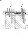
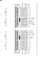
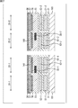
- FIG. 2 is a cross-sectional view illustrating a structure example of a solid-state imaging device to which the present technology is applied.
- the solid-state imaging device in the example of FIG. 2 is configured by a stacked CIS (CMOS Image Sensor).
- An example in which 22 are installed adjacent to each other is shown.
- an interlayer film 33 is formed on the semiconductor substrate 31 on which the Si PD 32 is formed.
- a light shielding film 34 is provided at a boundary portion between adjacent pixels in order to shield light from the lens of the adjacent pixel.
- a lower electrode 36, an organic photoelectric conversion film 37, and an upper electrode 38 are provided in this order from the bottom.
- an interlayer film 33 is formed on the semiconductor substrate 31 on which the Si PD 32 is formed.
- the interlayer film 33 is provided with a light shielding film 35 for shielding about half of the phase difference detection pixel 22, and further, a light incident side (interlayer film) outside the semiconductor substrate 31. 33) is not provided with an organic photoelectric conversion film.
- the organic photoelectric conversion film is actually removed on the light incident side (on the interlayer film 33).
- green light from the light incident side is absorbed by the organic photoelectric conversion film 37, and blue and red lights other than green mainly pass through the organic photoelectric conversion film 37, and Si PD 32. Is incident on.
- the organic photoelectric conversion film is not provided in the phase difference detection pixel 22, all the green, blue, and red light from the light incident side is incident on the Si PD 32. As a result, the Si PD 32 can receive more light than the imaging pixel 21, so that the phase difference detection accuracy can be improved.
- a transparent film such as a transparent organic material may be embedded.
- the structure above the upper electrode is also omitted, but in actuality, a passivation film such as SIN or an on-chip lens may be provided on the upper electrode.
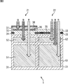
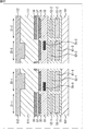
- FIG. 3 to 8 are cross-sectional views showing other structural examples of the solid-state imaging device.
- FIG. 3 is a diagram illustrating a structural example in which the shape of the lower electrode of the phase difference detection pixel is the same as that of the imaging pixel.
- the structure of the imaging pixel 21 is formed in the same manner as in the example of FIG. 2. Mainly, green light from the light incident side is absorbed by the organic photoelectric conversion film 37, and In addition, Blue and Red light other than Green passes through the organic photoelectric conversion film 37 and enters the Si PD 32.
- the lower electrode 41 has the same shape as the lower electrode 36 of the imaging pixel 21 on the interlayer film 33 provided with the light shielding film 35 for shielding half of the phase difference detection pixel 22. Is provided.
- phase difference detection pixel 22 of FIG. 3 since the organic photoelectric conversion film is not provided on the lower electrode 36, all the green, blue, and red light from the light incident side is incident on the Si PD 32. The As a result, the Si32PD 32 of the phase difference detection pixel 22 can receive more light than the imaging pixel 21, so that the phase difference detection accuracy can be improved.
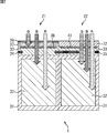
- FIG. 4 is a diagram illustrating a structure example in which two or more Si-PDs are stacked in the depth direction in the imaging pixel.
- the imaging pixel shown in FIG. 2 is that the Si PD 32 provided on the semiconductor substrate 31 is replaced with two Si PDs 51 and Si PDs 52 stacked in the depth direction. 21 is different. Therefore, in the imaging pixel 21, green light mainly from the light incident side is absorbed by the organic photoelectric conversion film 37, and blue and red light other than green mainly pass through the organic photoelectric conversion film 37. Then, the light enters the upper Si PD 52. Then, in the upper Si PD 52, mainly Blue light is absorbed, and most of the Red light is incident on the lower Si PD 51.
- the structure of the phase difference detection pixel 22 is formed in the same manner as in the example of FIG. 2, and the organic photoelectric conversion film is not provided on the light incident side (on the interlayer film 33) outside the semiconductor substrate 31.
- Si-PD is not limited to two layers, but may be three layers.
- FIG. 5 is a diagram showing a structure example in which two or more Si-PDs are stacked in the depth direction in the imaging pixel and the phase difference detection pixel.
- the structure of the imaging pixel 21 is formed in the same manner as in the example of FIG. 4.
- green light mainly from the light incident side is converted into an organic photoelectric conversion film.
- the blue and red light other than green is absorbed mainly by the light through the organic photoelectric conversion film 37 and incident on the upper Si PD 52.
- the upper Si PD 52 mainly Blue light is absorbed, and most of the Red light is incident on the lower Si PD 51.
- the point that the Si PD 32 provided on the semiconductor substrate 31 is replaced with two Si PD 61 and Si PD 62 that are stacked in the depth direction is the same as that of the imaging pixel 21 in FIG. 4. Is different. Therefore, one of Green, Blue, and Red light from the light incident side is incident on the Si PD 61, and one is incident on the Si PD 62.
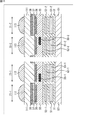
- FIG. 6 is a diagram showing a structural example in which a transparent film and an upper electrode are provided on an interlayer film in a phase difference detection pixel.
- the structure of the imaging pixel 21 is formed similarly to the example of FIG. 2, and green light mainly from the light incident side is absorbed by the organic photoelectric conversion film 37 and mainly. Blue and Red lights other than Green pass through the organic photoelectric conversion film 37 and enter the Si PD 32.
- phase difference detection pixel 22 a transparent material made of a transparent material having a high light transmittance in the visible light region is provided on the interlayer film 33 provided with the light shielding film 35 for shielding half of the phase difference detection pixel 22.
- a film 72 is disposed, and an upper electrode 71 is disposed on the transparent film 72.
- the upper electrode 71 can be formed simultaneously with the upper electrode 38 of the imaging pixel 21.
- the organic photoelectric conversion film is not disposed, but the transparent material and the upper electrode are formed. In this case, it is not necessary to process the upper electrode of the phase difference detection pixel portion, and the process construction is facilitated.
- FIG. 7 is a diagram showing a structural example in which a lower electrode and a transparent film are provided on an interlayer film in a phase difference detection pixel.
- the structure of the imaging pixel 21 is formed in the same manner as in the example of FIG. 2. Mainly, green light from the light incident side is absorbed by the organic photoelectric conversion film 37 and mainly. Blue and Red light other than Green passes through the organic photoelectric conversion film 37 and enters the organic photoelectric conversion film 37.
- the lower electrode 41 has the same shape as the lower electrode 36 of the imaging pixel 21 on the interlayer film 33 provided with the light shielding film 35 for shielding half of the phase difference detection pixel 22. Is provided.
- a transparent film 72 is disposed on the lower electrode 36.
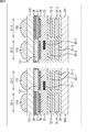
- FIG. 8 is a diagram showing a structural example in which a lower electrode, a transparent film, and an upper electrode are provided on an interlayer film in a phase difference detection pixel.
- the structure of the imaging pixel 21 is formed in the same manner as in the example of FIG. 2. Mainly, green light from the light incident side is absorbed by the organic photoelectric conversion film 37 and mainly. Blue and Red lights other than Green pass through the organic photoelectric conversion film 37 and enter the Si PD 32.
- the lower electrode 41 has the same shape as the lower electrode 36 of the imaging pixel 21 on the interlayer film 33 provided with the light shielding film 35 for shielding half of the phase difference detection pixel 22. Is provided.
- a transparent film 72 is provided on the lower electrode 36, and an upper electrode 71 formed simultaneously with the upper electrode 38 of the imaging pixel 21 is disposed on the transparent film 72.
- Si PD instead of Si PD, two types of Si PD shown in FIG. 4 or 5 may be vertically stacked.
- the organic photoelectric conversion film is not arranged in the phase difference detection pixel, that is, it is removed, so that the light in the wavelength band absorbed by the organic photoelectric conversion film is taken into the photodiode (Si PD),
- the sensitivity of the phase difference detection pixel can be improved.
- the material embedded as the transparent film 72 in the photoelectric conversion film removal region is, for example, a silicon nitride film, but other materials may be used.
- a film that absorbs as little light as possible For example, it is desirable to use a transparent film such as a silicon oxide film.
- an organic film when used as a photoelectric conversion film, it is necessary to prevent changes in film characteristics due to intrusion of moisture and gas (oxygen) from the processed end after etching the film. It is preferable to use a film having low properties, such as a silicon nitride film or alumina.
- a coating film having high flatness on the device surface after formation is used.
- an organic material film or silica that can be formed by coating can be used.
- planarization method a method in which the region where the photoelectric conversion film is removed is embedded with an insulating film and the entire surface of the device is planarized by CMP or etching is considered.
- CMP for example, scratching is performed after CMP. It is possible to use a silicon oxide film with less generation as a buried film.
- Si PD 51-1 and Si PD 52-1 are used for the imaging pixel 21-1, and Si61PD 61-1 and the phase difference detection pixel 22-1 are used.
- Si PD 62-1 is embedded, and Si PD 51-2 and Si PD 52-2 are used for imaging pixel 21-2, and Si PD 61-2 and Si PD 62-2 are used for phase difference detection pixel 22-2.
- An embedded semiconductor substrate 31 is prepared. On the semiconductor substrate 31, there is provided an interlayer film 33 on which a light shielding film 35-1 for the phase difference detection pixel 22-1 and a light shielding film 35-2 for the phase difference detection pixel 22-2 are formed. A lower electrode 36 is formed thereon.
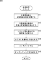
- step S ⁇ b> 11 the manufacturing apparatus deposits the organic photoelectric conversion film 37 and the upper electrode material to be the upper electrode 38 on the lower electrode 36.
- step S12 the manufacturing apparatus removes the organic photoelectric conversion film 37 and the upper electrode 38 of the phase difference detection pixels 22-1 and 22-2 as shown in FIG.
- step S13 although the phase difference detection pixels 22-1 and 22-2 are removed in the manufacturing apparatus, as shown in FIG. 12, for example, a silicon nitride film or the like is formed on the organic photoelectric conversion film 37. An interlayer film 111 is formed.
- step S14 as shown in FIG. 13, the manufacturing apparatus applies and planarizes a resist 112 on the interlayer film 111 formed in step S13.
- step S15 the manufacturing apparatus etches back the resist 112 applied in step S14 as shown in FIG.
- CMP is performed on the silicon nitride film that is the interlayer film 111
- scratches are likely to occur, which may cause image defects such as swirl.
- planarization can be performed without generation of scratches by performing planarization by the etch-back method.
- step S16 as shown in FIG. 15, the manufacturing apparatus forms an on-chip lens 113 on the interlayer film 111 planarized in step S14.
- the solid-state imaging device 1 is manufactured as described above.
- step S14 described above may be skipped, the interlayer film 111 may be CMPed in step S15, and the on-chip lens 113 may be formed in step S16.
- Steps S31 and S32 are the same processing as steps S11 and S12 of FIG.
- step S33 the manufacturing apparatus removes the phase difference detection pixels 22-1 and 22-2. As shown in FIG. 17, for example, a photosensitive material resin 131 is applied on the organic photoelectric conversion film 37. Apply.
- step S34 the manufacturing apparatus exposes and removes the photosensitive resin 131 other than the predetermined area (imaging pixels) as shown in FIG.
- step S35 the manufacturing apparatus applies a resist 132 to the entire surface as shown in FIG.
- step S36 the manufacturing apparatus etches back.
- the protruding portion of the photosensitive resin 131 may be polished by CMP.
- step S37 the manufacturing apparatus forms an interlayer film 133 as shown in FIG. 21, and forms an on-chip lens 113 on the formed interlayer film 133.
- the solid-state imaging device 1 is manufactured as described above.
- steps S35 and S36 described above are skipped, and in step S37, an interlayer film 133 is formed, and the on-chip lens 113 is formed on the formed interlayer film 133. You may do it.
- step S51 the manufacturing apparatus deposits the organic photoelectric conversion film 37 on the lower electrode.
- step S52 the manufacturing apparatus removes the organic photoelectric conversion film 37 of the phase difference detection pixels 22-1 and 22-2 as shown in FIG.
- a method in which a photosensitive material is mixed in the photoelectric conversion film and removed by exposure, or a method in which a predetermined region is removed by lithography and etching is used.
- step S53 the manufacturing apparatus applies the photosensitive resin 141 as shown in FIG.
- a photosensitive material is mixed into the organic photoelectric conversion film 37 in order to be removed by exposure.
- step S54 the manufacturing apparatus exposes and removes the photosensitive resin 141 other than the predetermined area as shown in FIG. At this time, a predetermined region can also be removed by lithography and etching.
- step S55 the manufacturing apparatus forms the upper electrode 38 as shown in FIG.
- step S56 the manufacturing apparatus forms an interlayer film on the upper electrode 38
- step S57 the on-chip lens 113 is formed on the formed interlayer film.
- the solid-state imaging device 1 is manufactured as described above.
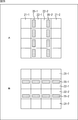
- 28 and 29 are plan views showing the top layout of the solid-state imaging device of the present technology.
- the phase difference detection pixels are adjacent to each other on the left and right.
- the first column is a column in which the imaging pixels 21-1 are arranged
- the second column from the left is a column in which the phase difference detection pixels 22-1 having the light shielding film 35-1 are arranged. is there.
- the third column from the left is a column in which the phase difference detection pixels 22-2 having the light shielding film 35-2 are arranged, and the imaging pixel 21-2 is arranged in the fourth column from the left. Is a column.
- the phase difference detection pixels are adjacent to each other in the vertical direction.
- the top row is the row where the imaging pixel 21-1 is arranged
- the second row from the top is the row where the phase difference detection pixel 22-1 having the light shielding film 35-1 is arranged. It is.
- the third row from the top is the row where the phase difference detection pixels 22-2 having the light shielding film 35-2 are arranged
- the fourth row from the top is arranged the imaging pixels 21-2. Line.
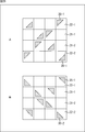
- the phase difference detection pixels are arranged on a 4 ⁇ 4 diagonal line.
- the light shielding films 35-1 and 35-2 are triangular and are formed so as to cover approximately half of the pixels.
- phase difference detection pixels 22-2 are formed so that the light shielding film 35-2 is formed on the lower right side on the diagonal line from the upper left to the lower right (oblique direction).
- phase difference detection pixels 22-1 are arranged on the diagonal line from the upper right to the lower left so that the light shielding film 35-1 is formed on the upper left side.
- phase difference detection pixels 22-2 are formed so that the light shielding film 35-2 is formed on the lower left side on the diagonal line from the upper left to the lower right (oblique direction).
- four phase difference detection pixels 22-1 are arranged on the diagonal line from the upper right to the lower left so that the light shielding film 35-1 is formed on the upper right side.
- the positions of the light shielding films 35-1 and 35-2 in the phase difference detection pixels 22-1 and 22-2 are different.
- the step film property of the embedded film when removing the photoelectric conversion film on the phase difference detection pixel, it is necessary to improve the step film property of the embedded film in order to prevent intrusion of moisture and gas (oxygen) from the end.
- the left and right opening patterns of the phase difference detection pixels are arranged in adjacent pixels, and the area of the photoelectric conversion film is made as large as possible to reduce the aspect of the embedded portion.
- the step film property of the embedded film can be improved, and the intrusion of moisture and gas (oxygen) from the side wall can be suppressed.
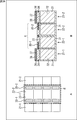
- FIG. 30A is a plan view showing a top layout of the solid-state imaging device of the present technology
- FIG. 30B is a cross-sectional view.
- the phase difference detection pixels 22-1 and 22-2 are arranged adjacent to each other on the left and right. By doing in this way, as shown by the dotted line E, the area
- FIG. 31A is a plan view showing a top layout of the solid-state imaging device
- FIG. 31B is a cross-sectional view.
- the imaging pixel 21-1, the phase difference detection pixel 22-1, the imaging pixel 21-2, and the phase difference detection pixel 22-2 are used. Pixels and phase difference detection pixels are alternately arranged.
- the region from which the photoelectric conversion film is removed becomes narrower than in the case of A in FIG. 30 and B in FIG.
- phase difference detection pixel since there is no organic film on the light irradiation side in the phase difference detection pixel, all RGB light can be incident on the photodiode. Thereby, the accuracy of phase difference detection, that is, focus detection can be improved.
- the longitudinal spectral sensor can obtain all RGB light information in one pixel.
- a sensor that is not in the vertical direction can obtain information of one RGB light with one pixel. Therefore, by applying the present technology to a sensor for longitudinal spectroscopy, the amount of signal obtained by one pixel is larger than that for a sensor that is not longitudinal spectroscopy, so that the accuracy of focus detection can be improved.
- FIG. 32 is a diagram illustrating a usage example in which the above-described solid-state imaging device is used.
- the solid-state imaging device (image sensor) described above can be used in various cases for sensing light such as visible light, infrared light, ultraviolet light, and X-ray as follows.
- Devices for taking images for viewing such as digital cameras and mobile devices with camera functions
- Devices used for traffic such as in-vehicle sensors that capture the back, surroundings, and interiors of vehicles, surveillance cameras that monitor traveling vehicles and roads, and ranging sensors that measure distances between vehicles, etc.
- Equipment used for home appliances such as TVs, refrigerators, air conditioners, etc. to take pictures and operate the equipment according to the gestures ⁇ Endoscopes, equipment that performs blood vessel photography by receiving infrared light, etc.
- Equipment used for medical and health care ⁇ Security equipment such as security surveillance cameras and personal authentication cameras ⁇ Skin measuring instrument for photographing skin and scalp photography Such as a microscope to do beauty Equipment used for sports-Equipment used for sports such as action cameras and wearable cameras for sports applications-Used for agriculture such as cameras for monitoring the condition of fields and crops apparatus
- the present technology is not limited to application to a solid-state imaging device, but can also be applied to an imaging device.
- the imaging apparatus refers to a camera system such as a digital still camera or a digital video camera, or an electronic apparatus having an imaging function such as a mobile phone.
- a module-like form mounted on an electronic device that is, a camera module is used as an imaging device.
- the 33 includes a solid-state imaging device (element chip) 301, an optical lens 302, a shutter device 303, a drive circuit 304, and a signal processing circuit 305.
- the solid-state imaging device 301 the solid-state imaging device 1 according to the first embodiment of the present technology described above is provided. Thereby, the reliability of the solid-state imaging device 301 of the electronic device 300 can be improved.
- the optical lens 302 forms image light (incident light) from the subject on the imaging surface of the solid-state imaging device 301. As a result, signal charges are accumulated in the solid-state imaging device 301 for a certain period.
- the shutter device 303 controls the light irradiation period and the light shielding period for the solid-state imaging device 301.
- the drive circuit 304 supplies a drive signal for controlling the signal transfer operation of the solid-state imaging device 301 and the shutter operation of the shutter device 303.
- the solid-state imaging device 301 performs signal transfer by a drive signal (timing signal) supplied from the drive circuit 304.
- the signal processing circuit 305 performs various signal processing on the signal output from the solid-state imaging device 301.
- the video signal subjected to the signal processing is stored in a storage medium such as a memory or output to a monitor.
- the configuration described as one device (or processing unit) may be divided and configured as a plurality of devices (or processing units).
- the configurations described above as a plurality of devices (or processing units) may be combined into a single device (or processing unit).
- a configuration other than that described above may be added to the configuration of each device (or each processing unit).
- a part of the configuration of a certain device (or processing unit) may be included in the configuration of another device (or other processing unit). . That is, the present technology is not limited to the above-described embodiment, and various modifications can be made without departing from the gist of the present technology.
- this technique can also take the following structures.
- a substrate on which a photoelectric conversion unit is formed An imaging region composed of a plurality of pixels arranged two-dimensionally on the substrate, The plurality of pixels include an imaging pixel formed between the substrate and the light incident side, which uses an organic photoelectric conversion film that absorbs light in a certain wavelength band, and the substrate and the light incident side.
- the phase difference detection pixel includes a light-shielding film that covers a substantially half region of the pixel between the substrate and the light incident side.
- the transparent film is made of a material having a high light transmittance in a visible light region.
- the transparent film is made of a material that absorbs less light.
- phase difference detection pixel includes at least one of an upper electrode and a lower electrode.
- phase difference detection pixel in the pair of pixels is disposed adjacent to the phase difference detection pixel in the other pair of pixels.
- Imaging device. The phase difference detection pixels in the pair of pixels are arranged at adjacent positions on the left and right sides of the phase difference detection pixels in the other pair of pixels according to any one of (1) to (9).
- Solid-state imaging device. (11) The phase difference detection pixels in the pair of pixels are arranged at adjacent positions above and below the phase difference detection pixels in the other pair of pixels. Solid-state imaging device.
- the phase difference detection pixel in the pair of pixels is disposed at an obliquely adjacent position with the phase difference detection pixel in the other pair of pixels.
- Solid-state imaging device (13) The solid-state imaging device according to any one of (1) to (12), wherein the organic photoelectric conversion film absorbs green light.
- a substrate on which a photoelectric conversion unit is formed a substrate on which a photoelectric conversion unit is formed;
- An imaging region composed of a plurality of pixels arranged two-dimensionally on the substrate, The plurality of pixels include an imaging pixel formed between the substrate and the light incident side, which uses an organic photoelectric conversion film that absorbs light in a certain wavelength band, and the substrate and the light incident side.
- a solid-state imaging device including a pair of pixels including a phase difference detection pixel from which the formed organic photoelectric conversion film is removed; A signal processing circuit for processing an output signal output from the solid-state imaging device; And an optical system that makes incident light incident on the solid-state imaging device.
- 1 solid-state imaging device 2 pixels, 3 pixel area, 11 semiconductor substrate, 21 imaging pixels, 22 phase difference detection pixels, 31 semiconductor substrate, 32 Si PD, 33 interlayer film, 34 light shielding film, 35 light shielding film, 36 lower electrode , 37 organic photoelectric conversion film, 38 upper electrode, 51, 52, 61, 62 Si PD, 71 upper electrode, 72 transparent film, 111 interlayer film, 112 resist, 113 on-chip lens, 131 photosensitive material resin, 132 resist, 133 Interlayer film, 141 photosensitive resin, 300 electronic equipment, 301 solid-state imaging device, 302 optical lens, 303 shutter device, 304 drive circuit, 305 signal processing circuit
Landscapes
- Engineering & Computer Science (AREA)
- Multimedia (AREA)
- Signal Processing (AREA)
- Physics & Mathematics (AREA)
- General Physics & Mathematics (AREA)
- Optics & Photonics (AREA)
- Solid State Image Pick-Up Elements (AREA)
Abstract
本開示は、焦点検出の精度を向上させることができるようにする固体撮像装置および電子機器に関する。 位相差検出画素においては、撮像用画素と同様に、Si PDが形成された半導体基板上に、層間膜が形成されている。しかしながら、撮像用画素と異なり、層間膜には、位相差検出画素の半分を遮光するための遮光膜35が設けられており、さらに、半導体基板外の光入射側(層間膜上)に有機光電変換膜が設けられていない。本開示は、例えば、有機膜を光電変換部に用いられるCMOS固体撮像装置に適用することができる。
Description
本開示は、固体撮像装置および電子機器に関し、特に、焦点検出の精度を向上させるようにした固体撮像装置および電子機器に関する。
Si外部に光電変換膜を有し、また、位相差検出用の画素を有する固体撮像装置がある。
例えば、特許文献1には、有機光電変換膜上部に遮光膜を分割することで、位相差検出を行う固体撮像装置が記載されている。また、特許文献2には、有機膜下部に、位相差検出用のセンサを設けることが記載されている。
しかしながら、特許文献1に記載の固体撮像装置の場合、有機光電変換膜直上での遮光膜形成や加工には、腹応力やダメージの抑制からプロセス的な制約が多く、実際の形成が困難であった。
特許文献2に記載の固体撮像装置の場合、位相差検出画素のSiより光入射側に、ある波長の光を吸収する材料があるため、Si PDに入射する光量が減少し、焦点検出精度が低下してしまっていた。また、特許文献2の技術は、積層型センサへの適用が困難であった。
本開示は、このような状況に鑑みてなされたものであり、焦点検出の精度を向上させることができるものである。
本技術の一側面の固体撮像装置は、光電変換部が形成された基板と、前記基板上に2次元状にそれぞれ配列された複数の画素からなる撮像領域とを備え、前記複数の画素は、前記基板と光入射側との間に形成された、ある波長帯の光を吸収する有機光電変換膜が用いられる撮像用画素と、前記基板と光入射側との間に形成された前記有機光電変膜が除去される位相差検出画素とからなる1対の画素で構成される。
前記位相差検出画素は、前記基板と光入射側との間に画素の略半分の領域を覆う遮光膜を有することができる。
前記位相差検出画素は、前記有機光電変換膜が除去された位置に対応する位置に透明な膜を有することができる。
前記透明な膜は、可視光領域の光の透過率が高い材料で構成される。
前記透明な膜は、光吸収が少ない材料で構成される。
前記透明な膜は、水分およびガスの透過性の低い材料で構成される。
前記透明な膜は、平坦化性が高い材料で構成される。
前記位相差検出画素は、上部電極および下部電極の少なくとも1つを有することができる。
前記1対の画素における前記位相差検出画素は、他の1対の画素における前記位相差検出画素と隣接位置に配置される。
前記1対の画素における前記位相差検出画素は、他の1対の画素における前記位相差検出画素と左右の隣接位置に配置される。
前記1対の画素における前記位相差検出画素は、他の1対の画素における前記位相差検出画素と上下の隣接位置に配置される。
前記1対の画素における前記位相差検出画素は、他の1対の画素における前記位相差検出画素と斜めの隣接位置に配置される。
前記有機光電変換膜は、Greenの光を吸収することができる。
前記撮像用画素および位相差検出画素の少なくともどちらか一方における前記光電変換部は、深さ方向に複数積層されている。
本発明の一側面の電子機器は、光電変換部が形成された基板と、前記基板上に2次元状にそれぞれ配列された複数の画素からなる撮像領域とを備え、前記複数の画素は、前記基板と光入射側との間に形成された、ある波長帯の光を吸収する有機光電変換膜が用いられる撮像用画素と、前記基板と光入射側との間に形成された前記有機光電変膜が除去される位相差検出画素とからなる1対の画素で構成される固体撮像装置と、前記固体撮像装置から出力される出力信号を処理する信号処理回路と、入射光を前記固体撮像装置に入射する光学系とを有する。
本技術の一側面においては、光電変換部が形成された基板上に2次元状にそれぞれ配列された複数の画素からなる撮像領域の複数の画素が、前記基板と光入射側との間に形成された、ある波長帯の光を吸収する有機光電変換膜が用いられる撮像用画素と、前記基板と光入射側との間に形成された前記有機光電変膜が除去される位相差検出画素とからなる1対の画素で構成される。
本技術によれば、焦点検出の精度を向上させることができる。本技術によれば、焦点検出の精度をさらに高めることができる。
なお、本明細書に記載された効果は、あくまで例示であり、本技術の効果は、本明細書に記載された効果に限定されるものではなく、付加的な効果があってもよい。
以下、本開示を実施するための形態(以下実施の形態とする)について説明する。なお、説明は以下の順序で行う。
1.第1の実施の形態(固体撮像装置の例)
2.第2の実施の形態(イメージセンサの使用例)
3.第3の実施の形態(電子機器の例)
1.第1の実施の形態(固体撮像装置の例)
2.第2の実施の形態(イメージセンサの使用例)
3.第3の実施の形態(電子機器の例)
<1.第1の実施の形態(固体撮像装置の例)>
<固体撮像装置の概略構成例>
図1は、本技術の各実施の形態に適用されるCMOS(Complementary Metal Oxide Semiconductor)固体撮像装置の一例の概略構成例を示している。
<固体撮像装置の概略構成例>
図1は、本技術の各実施の形態に適用されるCMOS(Complementary Metal Oxide Semiconductor)固体撮像装置の一例の概略構成例を示している。
図1に示されるように、固体撮像装置(素子チップ)1は、半導体基板11(例えばシリコン基板)に複数の光電変換素子(Si PD)を含む画素2が規則的に2次元的に配列された画素領域(いわゆる撮像領域)3と、周辺回路部とを有して構成される。
画素2は、光電変換素子(例えばフォトダイオード)と、複数の画素トランジスタ(いわゆるMOSトランジスタ)を有してなる。複数の画素トランジスタは、例えば、転送トランジスタ、リセットトランジスタ、および増幅トランジスタの3つのトランジスタで構成することができ、さらに選択トランジスタを追加して4つのトランジスタで構成することもできる。各画素2(単位画素)の等価回路は一般的なものと同様であるので、ここでは詳細な説明は省略する。
また、画素2は、共有画素構造とすることもできる。画素共有構造は、複数のフォトダイオード、複数の転送トランジスタ、共有される1つのフローティングディフュージョン、および、共有される1つずつの他の画素トランジスタから構成される。
周辺回路部は、垂直駆動回路4、カラム信号処理回路5、水平駆動回路6、出力回路7、および制御回路8から構成される。
制御回路8は、入力クロックや、動作モード等を指令するデータを受け取り、また、固体撮像装置1の内部情報等のデータを出力する。具体的には、制御回路8は、垂直同期信号、水平同期信号、およびマスタクロックに基づいて、垂直駆動回路4、カラム信号処理回路5、および水平駆動回路6の動作の基準となるクロック信号や制御信号を生成する。そして、制御回路8は、これらの信号を垂直駆動回路4、カラム信号処理回路5、および水平駆動回路6に入力する。
垂直駆動回路4は、例えばシフトレジスタによって構成され、画素駆動配線を選択し、選択された画素駆動配線に画素2を駆動するためのパルスを供給し、行単位で画素2を駆動する。具体的には、垂直駆動回路4は、画素領域3の各画素2を行単位で順次垂直方向に選択走査し、垂直信号線9を通して各画素2の光電変換素子において受光量に応じて生成した信号電荷に基づいた画素信号をカラム信号処理回路5に供給する。
カラム信号処理回路5は、画素2の例えば列毎に配置されており、1行分の画素2から出力される信号を画素列毎にノイズ除去等の信号処理を行う。具体的には、カラム信号処理回路5は、画素2固有の固定パターンノイズを除去するためのCDS(Correlated Double Sampling)や、信号増幅、A/D(Analog/Digital)変換等の信号処理を行う。カラム信号処理回路5の出力段には、水平選択スイッチ(図示せず)が水平信号線10との間に接続されて設けられる。
水平駆動回路6は、例えばシフトレジスタによって構成され、水平走査パルスを順次出力することによって、カラム信号処理回路5の各々を順番に選択し、カラム信号処理回路5の各々から画素信号を水平信号線10に出力させる。
出力回路7は、カラム信号処理回路5の各々から水平信号線10を通して順次に供給される信号に対し、信号処理を行って出力する。出力回路7は、例えば、バッファリングだけを行う場合もあるし、黒レベル調整、列ばらつき補正、各種デジタル信号処理等を行う場合もある。
入出力端子12は、外部と信号のやりとりをするために設けられる。
<固体撮像装置の構造例>
図2は、本技術を適用した固体撮像装置の構造例を示す断面図である。図2の例の固体撮像装置は、積層型のCIS(CMOS Image Sensor)で構成されている。
図2は、本技術を適用した固体撮像装置の構造例を示す断面図である。図2の例の固体撮像装置は、積層型のCIS(CMOS Image Sensor)で構成されている。
図2の例においては、取得された情報が撮像用に用いられる画素である撮像用画素21、および、取得された情報が位相差検出(焦点検出)用に用いられる画素である位相差検出画素22が隣接して設置されている例が示されている。
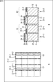
撮像用画素21においては、Si PD32が形成された半導体基板31上に、層間膜33が形成されている。層間膜33には、隣の画素のレンズからの光を遮光するために、隣接する画素との境界部分に遮光膜34が設けられている。半導体基板31外の光入射側である層間膜33上には、下部電極36、有機光電変換膜37、および上部電極38が下から順に設けられている。
一方、位相差検出画素22においては、撮像用画素21と同様に、Si PD32が形成された半導体基板31上に、層間膜33が形成されている。ただし、撮像用画素21と異なり、層間膜33には、位相差検出画素22の略半分を遮光するための遮光膜35が設けられており、さらに、半導体基板31外の光入射側(層間膜33上)に有機光電変換膜が設けられていない。詳しくは後述するが、実際には、位相差検出画素22においては、光入射側(層間膜33上)に有機光電変換膜が除かれている。
撮像用画素21においては、光入射側からのGreenの光が、有機光電変換膜37で吸収されて、主にGreen以外のBlueおよびRedの光が、有機光電変換膜37を通過し、Si PD32に入射される。
一方、位相差検出画素22においては、有機光電変換膜が設けられていないため、光入射側からのGreen、Blue、Redのすべての光が、Si PD32に入射される。これにより、Si PD32においては、撮像用画素21よりも多くの光を受光することができるので、位相差検出精度を向上させることができる。
なお、図2の例においては、位相差検出画素においては、有機光電変換膜がないことで、隣接する撮像用画素21との間に段差が生じているが、後述するように、SiN,SiO2,透明な有機材料などの透明な膜を埋め込むようにしてもよい。また、図2の例においては、上部電極より上の構造も省略されているが、実際には、上部電極上にはSIN等のパッシベーション膜やオンチップレンズが備えられるようにしてもよい。
図3乃至図8は、固体撮像装置の他の構造例を示す断面図である。図3は、位相差検出画素の下部電極の形状が、撮影用画素と同様である構造例を示す図である。
図3の例においては、撮像用画素21の構造は、図2の例と同様に形成されており、主に光入射側からのGreenの光が、有機光電変換膜37で吸収されて、主にGreen以外のBlueおよびRedの光が、有機光電変換膜37を通過し、Si PD32に入射される。
一方、位相差検出画素22においては、位相差検出画素22の半分を遮光するための遮光膜35が設けられた層間膜33上に下部電極41が、撮像用画素21の下部電極36と同じ形状で設けられている。
図3の位相差検出画素22においても、下部電極36上には、有機光電変換膜が設けられていないため、光入射側からのGreen、Blue、Redのすべての光が、Si PD32に入射される。これにより、位相差検出画素22のSi PD32においては、撮像用画素21よりも多くの光を受光することができるので、位相差検出精度を向上させることができる。
図4は、撮影用画素において、Si PDが深さ方向に2つ以上積層されている構造例を示す図である。
図4の例の撮像用画素21においては、半導体基板31に設けられたSi PD32が、深さ方向に2つ積層されているSi PD51およびSi PD52に入れ替わった点が、図2の撮像用画素21と異なっている。したがって、撮像用画素21においては、主に光入射側からのGreenの光が、有機光電変換膜37で吸収されて、主にGreen以外のBlueおよびRedの光が、有機光電変換膜37を通過し、上層のSi PD52に入射される。そして、上層のSi PD52において、主にBlueの光が吸収されて、Redの光の多くが、下層のSi PD51に入射される。
一方、位相差検出画素22の構造は図2の例と同様に形成されており、半導体基板31外の光入射側(層間膜33上)に有機光電変換膜が設けられていない。
したがって、図4の例においては、撮像用画素における縦方向分光を実現するとともに、位相差検出画素における高感度による焦点検出精度向上が期待できる。
なお、Si PDは、2層に限定されず、3層であってもよい。
図5は、撮影用画素および位相差検出画素において、Si PDが深さ方向に2つ以上積層されている構造例を示す図である。
図5の例においては、撮像用画素21の構造は、図4の例と同様に形成されており、撮像用画素21においては、主に光入射側からのGreenの光が、有機光電変換膜37で吸収されて、主にGreen以外のBlueおよびRedの光が、有機光電変換膜37を通過し、上層のSi PD52に入射される。そして、上層のSi PD52において、主にBlueの光が吸収されて、Redの光の多くが、下層のSi PD51に入射される。
一方、位相差検出画素22においても、半導体基板31に設けられたSi PD32が、深さ方向に2つ積層されているSi PD61およびSi PD62に入れ替わった点が、図4の撮像用画素21と異なっている。したがって、光入射側からのGreen、Blue、Redの光のうちいずれかが、Si PD61に入射され、いずれかがSi PD62に入射される。
したがって、図5の例の場合、撮像用画素における縦方向分光を実現するとともに、位相差検出画素も、撮像用画素と同じ構造にすることで、工程数を抑制することが可能となる。
図6は、位相差検出画素において、層間膜上に透明膜と上部電極が設けられる構造例を示す図である。
図6の例において、撮像用画素21の構造は、図2の例と同様に形成されており、主に光入射側からのGreenの光が、有機光電変換膜37で吸収されて、主にGreen以外のBlueおよびRedの光が、有機光電変換膜37を通過し、Si PD32に入射される。
一方、位相差検出画素22においては、位相差検出画素22の半分を遮光するための遮光膜35が設けられた層間膜33上に、可視光領域の光の透過率が高い透明材料でなる透明膜72が配置され、透明膜72の上に上部電極71が配置されている。この上部電極71は、撮像用画素21の上部電極38と同時に形成可能である。
以上のように、図6の位相差検出画素において、有機光電変換膜は配置されないが、透明材料および上部電極が形成される。この場合、位相差検出画素部分の上部電極の加工が不要となり、プロセス構築が容易となる。
図7は、位相差検出画素において、層間膜上に下部電極と透明膜とが設けられる構造例を示す図である。
図7の例において、撮像用画素21の構造は、図2の例と同様に形成されており、主に光入射側からのGreenの光が、有機光電変換膜37で吸収されて、主にGreen以外のBlueおよびRedの光が、有機光電変換膜37を通過し、に入射される。
一方、位相差検出画素22においては、位相差検出画素22の半分を遮光するための遮光膜35が設けられた層間膜33上に下部電極41が、撮像用画素21の下部電極36と同じ形状で設けられている。そして、下部電極36の上には、透明膜72が配置されている。
図8は、位相差検出画素において、層間膜上に、下部電極、透明膜、および上部電極が設けられる構造例を示す図である。
図8の例において、撮像用画素21の構造は、図2の例と同様に形成されており、主に光入射側からのGreenの光が、有機光電変換膜37で吸収されて、主にGreen以外のBlueおよびRedの光が、有機光電変換膜37を通過し、Si PD32に入射される。
一方、位相差検出画素22においては、位相差検出画素22の半分を遮光するための遮光膜35が設けられた層間膜33上に下部電極41が、撮像用画素21の下部電極36と同じ形状で設けられている。そして、下部電極36の上には、透明膜72が設けられ、透明膜72の上に、撮像用画素21の上部電極38と同時に形成される上部電極71が配置されている。
なお、図6乃至図8の例においては、Si PDに代えて、図4または図5の2種類のSi PDを縦型積層する構造にしてもよい。
以上のように、位相差検出画素に有機光電変換膜を配置しない、すなわち、除去するようにしたので、有機光電変換膜で吸収されていた波長帯の光をフォトダイオード(Si PD)に取り込み、位相差検出画素の感度を向上させることができる。
また、図6乃至図8の例のように、透明な膜などを埋め込むことにより、撮像用画素と位相差検出画素との間に段差を生じないようにしたので、マイクロレンズなどの特性が変わることを抑制することができる。
なお、光電変換膜除去領域に透明膜72として埋め込む材料は、例えば、シリコン窒化膜としたが、他の材料であってもよい。位相差検出画素の感度を向上させるという目的のため、できるだけ光の吸収の少ない膜であることが望ましく、例えば、シリコン酸化膜などの透明な膜を用いることが望ましい。
また、光電変換膜として有機膜を用いる場合、膜をエッチング除去した加工端部からの水分やガス(酸素)の侵入による膜特性の変化を防止する必要がある、水分やガス(酸素)の透過性の低い膜、例えば、シリコン窒化膜やアルミナなどを用いることが好ましい。
さらに、光電変換膜を形成しない領域を埋め込む場合、埋め込み後の装置の平坦性を高めることが望ましい。これは、その後に形成されるオンチップマイクロレンズ加工時に平坦性の高い方が、リソグラフィやエッチングによる加工均一性を高めるために有効なためである。このために、形成後のデバイス表面の平坦性が高い塗布膜が用いられる。この場合、塗布形成が可能な有機材料膜やシリカなどを用いることができる。
また、別の平坦化方法としては、光電変換膜を抜いた領域を絶縁膜で埋め込み、装置全面を、CMPやエッチングで平坦化する方法が考えられるが、CMPを用いる場合、例えば、CMP後にスクラッチの発生が少ないシリコン酸化膜を、埋め込み膜として用いることが可能である。
次に、図9のフローチャートを参照して、本技術の固体撮像装置の製造処理の一例について説明する。なお、この処理は、図示せぬ固体撮像装置の製造装置により行われる。
図10に示されるように、層間絶縁膜101上に、撮像用画素21-1用として、Si PD51-1およびSi PD52-1と、位相差検出画素22-1用として、Si PD61-1およびSi PD62-1とが埋め込まれ、撮像用画素21-2用として、Si PD51-2およびSi PD52-2と、位相差検出画素22-2用として、Si PD61-2およびSi PD62-2とが埋め込まれた半導体基板31が用意されている。そして、その半導体基板31上に、位相差検出画素22-1用の遮光膜35-1と、位相差検出画素22-2用の遮光膜35-2とが形成された層間膜33が設けられ、その上に下部電極36が形成されている。
ステップS11において、製造装置は、下部電極36上に、有機光電変換膜37と、上部電極38となる上部電極材料を被着する。
ステップS12において、製造装置は、図11に示されるように、位相差検出画素22-1および22-2の有機光電変換膜37と上部電極38とを除去する。
ステップS13において、製造装置は、位相差検出画素22-1および22-2については除去されているが、有機光電変換膜37上に、図12に示されるように、例えば、シリコン窒化膜などの層間膜111を成膜する。
ステップS14において、製造装置は、図13に示されるように、ステップS13において成膜された層間膜111上に、レジスト112を塗布し、平坦化する。
ステップS15において、製造装置は、図14に示されるように、ステップS14において塗布されたレジスト112をエッチバックする。なお、層間膜111であるシリコン窒化膜をCMPする場合、スクラッチが入りやすく、スワールなどの画像欠陥となる可能性がある。このような場合に、エッチバック法で平坦化することで、スクラッチの発生なく、平坦化を行うことができる。
ステップS16において、製造装置は、図15に示されるように、ステップS14において平坦化された層間膜111の上に、オンチップレンズ113を形成する。
以上のようにして、固体撮像装置1が製造される。
なお、他の製造処理としては、例えば、上述したステップS14をスキップして、ステップS15において層間膜111をCMPして、ステップS16において、オンチップレンズ113を形成するようにしてもよい。
次に、図16のフローチャートを参照して、本技術の固体撮像装置の製造処理の他の例について説明する。なお、ステップS31およびS32は、図9のステップS11およびS12と同じ処理であるので、その説明は省略される。
ステップS33において、製造装置は、位相差検出画素22-1および22-2については除去されているが、有機光電変換膜37上に、図17に示されるように、例えば、感光材樹脂131を塗布する。
ステップS34において、製造装置は、露光し、図18に示されるように、所定領域以外(撮像用画素)の感光性樹脂131を除去する。ステップS35において、製造装置は、図19に示されるように、全面にレジスト132を塗布する。
ステップS36において、製造装置は、エッチバックする。なお、その際、CMPにより感光性樹脂131の突起部を研磨するようにしてもよい。感光性樹脂131の突起部をなくすことで、その後のオンチップレンズの形成などを容易に行うことができる。
ステップS37において、製造装置は、図21に示されるように、層間膜133を成膜し、成膜された層間膜133上にオンチップレンズ113を形成する。
以上のようにして、固体撮像装置1が製造される。
なお、他の製造処理としては、例えば、上述したステップS35およびS36をスキップして、ステップS37において、層間膜133を成膜し、成膜された層間膜133上にオンチップレンズ113を形成するようにしてもよい。
さらに、図22のフローチャートを参照して、本技術の固体撮像装置の製造処理のさらに他の例について説明する。
ステップS51において、製造装置は、下部電極36上に、有機光電変換膜37を被着する。ステップS52において、製造装置は、図24に示されるように、位相差検出画素22-1および22-2の有機光電変換膜37を除去する。ここでは、例えば、光電変換膜に感光性材料を混ぜて露光で除去する方法や、リソグラフィとエッチングで所定の領域を除去する方法が用いられる。
ステップS53において、製造装置は、図25に示されるように、感光性樹脂141を塗布する。例えば、露光で除去するために、有機光電変換膜37に感光性材料を混ぜる。
ステップS54において、製造装置は、露光し、図26に示されるように、所定領域以外の感光性樹脂141を除去する。なお、このとき、リソグラフィとエッチングで所定の領域も除去することができる。
ステップS55において、製造装置は、図27に示されるように、上部電極38を形成する。そして、製造装置は、ステップS56において、上部電極38上に、層間膜を成膜し、ステップS57において、成膜された層間膜上にオンチップレンズ113を形成する。
以上のようにして、固体撮像装置1が製造される。
図28および図29は、本技術の固体撮像装置の上面レイアウトを示す平面図である。
例えば、図28のAの例においては、位相差検出画素同士が左右で隣り合う例が示されている。例えば、1番目の列が、撮像用画素21-1が配置される列であり、左から2番目の列が、遮光膜35-1を有する位相差検出画素22-1が配置される列である。さらに、左から3番目の列が、遮光膜35-2を有する位相差検出画素22-2が配置される列であり、左から4番目の列が、撮像用画素21-2が配置される列である。
例えば、図28のBの例においては、位相差検出画素同士が上下で隣り合う例が示されている。例えば、1番上の行が、撮像用画素21-1が配置される行であり、上から2番目の行が、遮光膜35-1を有する位相差検出画素22-1が配置される行である。さらに、上から3番目の行が、遮光膜35-2を有する位相差検出画素22-2が配置される行であり、上から4番目の行が、撮像用画素21-2が配置される行である。
さらに、図29のAおよび図29のBの例においては、4×4における対角線上に位相差検出画素を配置した例が示されている。また、この例において、遮光膜35-1および35-2は、三角形状で、画素の略半分を覆うように形成されている。
図29のAの例の場合、例えば、左上から右下への対角線上(斜め方向)に、右下側に遮光膜35-2が形成されるように、位相差検出画素22-2が4つ配置されている。また、例えば、右上から左下への対角線上に、左上側に遮光膜35-1が形成されるように、位相差検出画素22-1が4つ配置されている。
図29のBの例の場合、例えば、左上から右下への対角線上(斜め方向)に、左下側に遮光膜35-2が形成されるように、位相差検出画素22-2が4つ配置されている。また、例えば、右上から左下への対角線上に、右上側に遮光膜35-1が形成されるように、位相差検出画素22-1が4つ配置されている。
すなわち、図29のAおよび図29のBの例は、位相差検出画素22-1および22-2における遮光膜35-1および35-2の位置が異なっている。
なお、ここで、位相差検出画素上の光電変換膜を除去する場合、端部からの水分やガス(酸素)の侵入を防ぐため、埋め込み膜の段差被膜性を高める必要がある。特に微細画素においては、埋め込み膜のカバレッジを向上させるために、位相差検出画素の左右開口パターンを隣接画素に配置し、光電変換膜の抜き領域をできるだけ大きくすることで、埋め込み部のアスペクトを低くし、埋め込み膜の段差被膜性を高め、側壁からの水分やガス(酸素)の侵入を抑制することができる。
図30のAは、本技術の固体撮像装置の上面レイアウトを示す平面図であり、図30のBは、断面図である。図30のAおよび図30のBの例においては、図28のAの例と同様に、位相差検出画素22-1および22-2が左右で隣接されて配置されている。このようにすることで、点線Eに示されるように、光電変換膜を抜く領域が広くなる。
これに対して、図31のAは、固体撮像装置の上面レイアウトを示す平面図であり、図31のBは、断面図である。図31のAおよび図31のBの例においては、撮像用画素21-1、位相差検出画素22-1、撮像用画素21-2、および位相差検出画素22-2のように、撮像用画素と位相差検出画素が交互に配置されている。この場合、点線E1と点線E2に示されるように、光電変換膜を抜く領域が図30のAおよび図30のBの場合と比して狭くなる。
以上のように、本技術によれば、位相差検出画素において、光照射側に有機膜がないので、RGBすべての光をフォトダイオードに入射させることができる。これにより、位相差検出、すなわち、焦点検出の精度を向上させることができる。
また、縦方向分光のセンサは、RGB全ての光の情報を1画素で得ることができる。縦方向分光ではないセンサは、RGBの1つの光の情報を1画素で得ることができる。したがって、縦方向分光のセンサに、本技術を適用することにより、縦方向分光でないセンサと比して、1画素で得られる信号量が多いため、焦点検出の精度を高めることができる。
<2.第2の実施の形態(イメージセンサの使用例)>
図32は、上述の固体撮像装置を使用する使用例を示す図である。
図32は、上述の固体撮像装置を使用する使用例を示す図である。
上述した固体撮像装置(イメージセンサ)は、例えば、以下のように、可視光や、赤外光、紫外光、X線等の光をセンシングする様々なケースに使用することができる。
・ディジタルカメラや、カメラ機能付きの携帯機器等の、鑑賞の用に供される画像を撮影する装置
・自動停止等の安全運転や、運転者の状態の認識等のために、自動車の前方や後方、周囲、車内等を撮影する車載用センサ、走行車両や道路を監視する監視カメラ、車両間等の測距を行う測距センサ等の、交通の用に供される装置
・ユーザのジェスチャを撮影して、そのジェスチャに従った機器操作を行うために、TVや、冷蔵庫、エアーコンディショナ等の家電に供される装置
・内視鏡や、赤外光の受光による血管撮影を行う装置等の、医療やヘルスケアの用に供される装置
・防犯用途の監視カメラや、人物認証用途のカメラ等の、セキュリティの用に供される装置
・肌を撮影する肌測定器や、頭皮を撮影するマイクロスコープ等の、美容の用に供される装置
・スポーツ用途等向けのアクションカメラやウェアラブルカメラ等の、スポーツの用に供される装置
・畑や作物の状態を監視するためのカメラ等の、農業の用に供される装置
・自動停止等の安全運転や、運転者の状態の認識等のために、自動車の前方や後方、周囲、車内等を撮影する車載用センサ、走行車両や道路を監視する監視カメラ、車両間等の測距を行う測距センサ等の、交通の用に供される装置
・ユーザのジェスチャを撮影して、そのジェスチャに従った機器操作を行うために、TVや、冷蔵庫、エアーコンディショナ等の家電に供される装置
・内視鏡や、赤外光の受光による血管撮影を行う装置等の、医療やヘルスケアの用に供される装置
・防犯用途の監視カメラや、人物認証用途のカメラ等の、セキュリティの用に供される装置
・肌を撮影する肌測定器や、頭皮を撮影するマイクロスコープ等の、美容の用に供される装置
・スポーツ用途等向けのアクションカメラやウェアラブルカメラ等の、スポーツの用に供される装置
・畑や作物の状態を監視するためのカメラ等の、農業の用に供される装置
<3.第3の実施の形態(電子機器の例)>
<電子機器の構成例>
<電子機器の構成例>
さらに、本技術は、固体撮像装置への適用に限られるものではなく、撮像装置にも適用可能である。ここで、撮像装置とは、デジタルスチルカメラやデジタルビデオカメラ等のカメラシステムや、携帯電話機等の撮像機能を有する電子機器のことをいう。なお、電子機器に搭載されるモジュール状の形態、すなわちカメラモジュールを撮像装置とする場合もある。
ここで、図33を参照して、本技術の第3の実施の形態の電子機器の構成例について説明する。
図33に示される電子機器300は、固体撮像装置(素子チップ)301、光学レンズ302、シャッタ装置303、駆動回路304、および信号処理回路305を備えている。固体撮像装置301としては、上述した本技術の第1の実施の形態の固体撮像装置1が設けられる。これにより、電子機器300の固体撮像装置301の信頼性を向上することができる。
光学レンズ302は、被写体からの像光(入射光)を固体撮像装置301の撮像面上に結像させる。これにより、固体撮像装置301内に一定期間信号電荷が蓄積される。シャッタ装置303は、固体撮像装置301に対する光照射期間および遮光期間を制御する。
駆動回路304は、固体撮像装置301の信号転送動作およびシャッタ装置303のシャッタ動作を制御する駆動信号を供給する。駆動回路304から供給される駆動信号(タイミング信号)により、固体撮像装置301は信号転送を行う。信号処理回路305は、固体撮像装置301から出力された信号に対して各種の信号処理を行う。信号処理が行われた映像信号は、メモリなどの記憶媒体に記憶されたり、モニタに出力される。
なお、本開示における実施の形態は、上述した実施の形態に限定されるものではなく、本開示の要旨を逸脱しない範囲において種々の変更が可能である。
また、以上において、1つの装置(または処理部)として説明した構成を分割し、複数の装置(または処理部)として構成するようにしてもよい。逆に、以上において複数の装置(または処理部)として説明した構成をまとめて1つの装置(または処理部)として構成されるようにしてもよい。また、各装置(または各処理部)の構成に上述した以外の構成を付加するようにしてももちろんよい。さらに、システム全体としての構成や動作が実質的に同じであれば、ある装置(または処理部)の構成の一部を他の装置(または他の処理部)の構成に含めるようにしてもよい。つまり、本技術は、上述した実施の形態に限定されるものではなく、本技術の要旨を逸脱しない範囲において種々の変更が可能である。
以上、添付図面を参照しながら本開示の好適な実施形態について詳細に説明したが、開示はかかる例に限定されない。本開示の属する技術の分野における通常の知識を有するのであれば、請求の範囲に記載された技術的思想の範疇内において、各種の変更例また修正例に想到し得ることは明らかであり、これらについても、当然に本開示の技術的範囲に属するものと了解される。
なお、本技術は以下のような構成も取ることができる。
(1) 光電変換部が形成された基板と、
前記基板上に2次元状にそれぞれ配列された複数の画素からなる撮像領域と
を備え、
前記複数の画素は、前記基板と光入射側との間に形成された、ある波長帯の光を吸収する有機光電変換膜が用いられる撮像用画素と、前記基板と光入射側との間に形成された前記有機光電変膜が除去される位相差検出画素とからなる1対の画素で構成される
固体撮像装置。
(2) 前記位相差検出画素は、前記基板と光入射側との間に画素の略半分の領域を覆う遮光膜を有する
前記(1)に記載の固体撮像装置。
(3) 前記位相差検出画素は、前記有機光電変換膜が除去された位置に対応する位置に透明な膜を有する
前記(1)または(2)に記載の固体撮像装置。
(4) 前記透明な膜は、可視光領域の光の透過率が高い材料で構成される
前記(3)に記載の固体撮像装置。
(5) 前記透明な膜は、光吸収が少ない材料で構成される
前記(3)または(4)に記載の固体撮像装置。
(6) 前記透明な膜は、水分およびガスの透過性の低い材料で構成される
前記(3)乃至(5)のいずれかに記載の固体撮像装置。
(7) 前記透明な膜は、平坦化性が高い材料で構成される
前記(3)乃至(6)のいずれかに記載の固体撮像装置。
(8) 前記位相差検出画素は、上部電極および下部電極の少なくとも1つを有する
前記(1)乃至(7)のいずれかに記載の固体撮像装置。
(9) 前記1対の画素における前記位相差検出画素は、他の1対の画素における前記位相差検出画素と隣接位置に配置される
前記(1)乃至(8)のいずれかに記載の固体撮像装置。
(10) 前記1対の画素における前記位相差検出画素は、他の1対の画素における前記位相差検出画素と左右の隣接位置に配置される
前記(1)乃至(9)のいずれかに記載の固体撮像装置。
(11) 前記1対の画素における前記位相差検出画素は、他の1対の画素における前記位相差検出画素と上下の隣接位置に配置される
前記(1)乃至(9)のいずれかに記載の固体撮像装置。
(12) 前記1対の画素における前記位相差検出画素は、他の1対の画素における前記位相差検出画素と斜めの隣接位置に配置される
前記(1)乃至(9)のいずれかに記載の固体撮像装置。
(13) 前記有機光電変換膜は、Greenの光を吸収する
前記(1)乃至(12)のいずれかに記載の固体撮像装置。
(14) 前記撮像用画素および位相差検出画素の少なくともどちらか一方における前記光電変換部は、深さ方向に複数積層されている
前記(1)乃至(13)のいずれかに記載の固体撮像装置。
(15) 光電変換部が形成された基板と、
前記基板上に2次元状にそれぞれ配列された複数の画素からなる撮像領域と
を備え、
前記複数の画素は、前記基板と光入射側との間に形成された、ある波長帯の光を吸収する有機光電変換膜が用いられる撮像用画素と、前記基板と光入射側との間に形成された前記有機光電変膜が除去される位相差検出画素とからなる1対の画素で構成される
固体撮像装置と、
前記固体撮像装置から出力される出力信号を処理する信号処理回路と、
入射光を前記固体撮像装置に入射する光学系と
を有する電子機器。
(1) 光電変換部が形成された基板と、
前記基板上に2次元状にそれぞれ配列された複数の画素からなる撮像領域と
を備え、
前記複数の画素は、前記基板と光入射側との間に形成された、ある波長帯の光を吸収する有機光電変換膜が用いられる撮像用画素と、前記基板と光入射側との間に形成された前記有機光電変膜が除去される位相差検出画素とからなる1対の画素で構成される
固体撮像装置。
(2) 前記位相差検出画素は、前記基板と光入射側との間に画素の略半分の領域を覆う遮光膜を有する
前記(1)に記載の固体撮像装置。
(3) 前記位相差検出画素は、前記有機光電変換膜が除去された位置に対応する位置に透明な膜を有する
前記(1)または(2)に記載の固体撮像装置。
(4) 前記透明な膜は、可視光領域の光の透過率が高い材料で構成される
前記(3)に記載の固体撮像装置。
(5) 前記透明な膜は、光吸収が少ない材料で構成される
前記(3)または(4)に記載の固体撮像装置。
(6) 前記透明な膜は、水分およびガスの透過性の低い材料で構成される
前記(3)乃至(5)のいずれかに記載の固体撮像装置。
(7) 前記透明な膜は、平坦化性が高い材料で構成される
前記(3)乃至(6)のいずれかに記載の固体撮像装置。
(8) 前記位相差検出画素は、上部電極および下部電極の少なくとも1つを有する
前記(1)乃至(7)のいずれかに記載の固体撮像装置。
(9) 前記1対の画素における前記位相差検出画素は、他の1対の画素における前記位相差検出画素と隣接位置に配置される
前記(1)乃至(8)のいずれかに記載の固体撮像装置。
(10) 前記1対の画素における前記位相差検出画素は、他の1対の画素における前記位相差検出画素と左右の隣接位置に配置される
前記(1)乃至(9)のいずれかに記載の固体撮像装置。
(11) 前記1対の画素における前記位相差検出画素は、他の1対の画素における前記位相差検出画素と上下の隣接位置に配置される
前記(1)乃至(9)のいずれかに記載の固体撮像装置。
(12) 前記1対の画素における前記位相差検出画素は、他の1対の画素における前記位相差検出画素と斜めの隣接位置に配置される
前記(1)乃至(9)のいずれかに記載の固体撮像装置。
(13) 前記有機光電変換膜は、Greenの光を吸収する
前記(1)乃至(12)のいずれかに記載の固体撮像装置。
(14) 前記撮像用画素および位相差検出画素の少なくともどちらか一方における前記光電変換部は、深さ方向に複数積層されている
前記(1)乃至(13)のいずれかに記載の固体撮像装置。
(15) 光電変換部が形成された基板と、
前記基板上に2次元状にそれぞれ配列された複数の画素からなる撮像領域と
を備え、
前記複数の画素は、前記基板と光入射側との間に形成された、ある波長帯の光を吸収する有機光電変換膜が用いられる撮像用画素と、前記基板と光入射側との間に形成された前記有機光電変膜が除去される位相差検出画素とからなる1対の画素で構成される
固体撮像装置と、
前記固体撮像装置から出力される出力信号を処理する信号処理回路と、
入射光を前記固体撮像装置に入射する光学系と
を有する電子機器。
1 固体撮像装置, 2 画素, 3 画素領域, 11 半導体基板, 21 撮像用画素, 22 位相差検出画素, 31 半導体基板, 32 Si PD, 33 層間膜, 34 遮光膜, 35 遮光膜, 36 下部電極, 37 有機光電変換膜, 38 上部電極, 51,52,61,62 Si PD, 71 上部電極, 72 透明膜, 111 層間膜, 112 レジスト, 113 オンチップレンズ, 131 感光材樹脂, 132 レジスト, 133 層間膜, 141 感光性樹脂, 300 電子機器, 301 固体撮像装置, 302 光学レンズ, 303 シャッタ装置, 304 駆動回路, 305 信号処理回路
Claims (15)
- 光電変換部が形成された基板と、
前記基板上に2次元状にそれぞれ配列された複数の画素からなる撮像領域と
を備え、
前記複数の画素は、前記基板と光入射側との間に形成された、ある波長帯の光を吸収する有機光電変換膜が用いられる撮像用画素と、前記基板と光入射側との間に形成された前記有機光電変膜が除去される位相差検出画素とからなる1対の画素で構成される
固体撮像装置。 - 前記位相差検出画素は、前記基板と光入射側との間に画素の略半分の領域を覆う遮光膜を有する
請求項1の記載の固体撮像装置。 - 前記位相差検出画素は、前記有機光電変換膜が除去された位置に対応する位置に透明な膜を有する
請求項1の記載の固体撮像装置。 - 前記透明な膜は、可視光領域の光の透過率が高い材料で構成される
請求項3の記載の固体撮像装置。 - 前記透明な膜は、光吸収が少ない材料で構成される
請求項3の記載の固体撮像装置。 - 前記透明な膜は、水分およびガスの透過性の低い材料で構成される
請求項3の記載の固体撮像装置。 - 前記透明な膜は、平坦化性が高い材料で構成される
請求項3の記載の固体撮像装置。 - 前記位相差検出画素は、上部電極および下部電極の少なくとも1つを有する
請求項2の記載の固体撮像装置。 - 前記1対の画素における前記位相差検出画素は、他の1対の画素における前記位相差検出画素と隣接位置に配置される
請求項1の記載の固体撮像装置。 - 前記1対の画素における前記位相差検出画素は、他の1対の画素における前記位相差検出画素と左右の隣接位置に配置される
請求項9の記載の固体撮像装置。 - 前記1対の画素における前記位相差検出画素は、他の1対の画素における前記位相差検出画素と上下の隣接位置に配置される
請求項9の記載の固体撮像装置。 - 前記1対の画素における前記位相差検出画素は、他の1対の画素における前記位相差検出画素と斜めの隣接位置に配置される
請求項9の記載の固体撮像装置。 - 前記有機光電変換膜は、Greenの光を吸収する
請求項1の記載の固体撮像装置。 - 前記撮像用画素および位相差検出画素の少なくともどちらか一方における前記光電変換部は、深さ方向に複数積層されている
請求項1の記載の固体撮像装置。 - 光電変換部が形成された基板と、
前記基板上に2次元状にそれぞれ配列された複数の画素からなる撮像領域と
を備え、
前記複数の画素は、前記基板と光入射側との間に形成された、ある波長帯の光を吸収する有機光電変換膜が用いられる撮像用画素と、前記基板と光入射側との間に形成された前記有機光電変膜が除去される位相差検出画素とからなる1対の画素で構成される
固体撮像装置と、
前記固体撮像装置から出力される出力信号を処理する信号処理回路と、
入射光を前記固体撮像装置に入射する光学系と
を有する電子機器。
Applications Claiming Priority (2)
| Application Number | Priority Date | Filing Date | Title |
|---|---|---|---|
| JP2015-111336 | 2015-06-01 | ||
| JP2015111336 | 2015-06-01 |
Publications (1)
| Publication Number | Publication Date |
|---|---|
| WO2016194620A1 true WO2016194620A1 (ja) | 2016-12-08 |
Family
ID=57441085
Family Applications (1)
| Application Number | Title | Priority Date | Filing Date |
|---|---|---|---|
| PCT/JP2016/064830 Ceased WO2016194620A1 (ja) | 2015-06-01 | 2016-05-19 | 固体撮像装置および電子機器 |
Country Status (1)
| Country | Link |
|---|---|
| WO (1) | WO2016194620A1 (ja) |
Cited By (3)
| Publication number | Priority date | Publication date | Assignee | Title |
|---|---|---|---|---|
| JP2018190946A (ja) * | 2017-05-01 | 2018-11-29 | 采▲ぎょく▼科技股▲ふん▼有限公司VisEra Technologies Company Limited | イメージセンサー |
| WO2019039010A1 (ja) * | 2017-08-22 | 2019-02-28 | ソニーセミコンダクタソリューションズ株式会社 | 固体撮像素子、固体撮像素子の製造方法、及び電子機器 |
| US10819929B2 (en) * | 2017-08-10 | 2020-10-27 | Samsung Electronics Co., Ltd. | Image sensor for compensating for signal difference between pixels |
Citations (2)
| Publication number | Priority date | Publication date | Assignee | Title |
|---|---|---|---|---|
| JP2015050331A (ja) * | 2013-09-02 | 2015-03-16 | ソニー株式会社 | 固体撮像素子およびその製造方法、並びに電子機器 |
| US20150146056A1 (en) * | 2013-11-27 | 2015-05-28 | Sony Corporation | Solid-state imaging device and electronic apparatus |
-
2016
- 2016-05-19 WO PCT/JP2016/064830 patent/WO2016194620A1/ja not_active Ceased
Patent Citations (2)
| Publication number | Priority date | Publication date | Assignee | Title |
|---|---|---|---|---|
| JP2015050331A (ja) * | 2013-09-02 | 2015-03-16 | ソニー株式会社 | 固体撮像素子およびその製造方法、並びに電子機器 |
| US20150146056A1 (en) * | 2013-11-27 | 2015-05-28 | Sony Corporation | Solid-state imaging device and electronic apparatus |
Cited By (5)
| Publication number | Priority date | Publication date | Assignee | Title |
|---|---|---|---|---|
| JP2018190946A (ja) * | 2017-05-01 | 2018-11-29 | 采▲ぎょく▼科技股▲ふん▼有限公司VisEra Technologies Company Limited | イメージセンサー |
| US12009379B2 (en) | 2017-05-01 | 2024-06-11 | Visera Technologies Company Limited | Image sensor |
| US10819929B2 (en) * | 2017-08-10 | 2020-10-27 | Samsung Electronics Co., Ltd. | Image sensor for compensating for signal difference between pixels |
| WO2019039010A1 (ja) * | 2017-08-22 | 2019-02-28 | ソニーセミコンダクタソリューションズ株式会社 | 固体撮像素子、固体撮像素子の製造方法、及び電子機器 |
| US11240450B2 (en) | 2017-08-22 | 2022-02-01 | Sony Semiconductor Solutions Corporation | Solid-state imaging element, method for manufacturing solid-state imaging element, and electronic apparatus |
Similar Documents
| Publication | Publication Date | Title |
|---|---|---|
| US12166057B2 (en) | Solid-state imaging device, manufacturing method thereof, and electronic device | |
| JP7375852B2 (ja) | 固体撮像素子およびその製造方法、並びに電子機器 | |
| JP7264187B2 (ja) | 固体撮像装置およびその駆動方法、並びに電子機器 | |
| JP6987950B2 (ja) | 固体撮像素子およびその製造方法、並びに電子機器 | |
| JP6721511B2 (ja) | 固体撮像素子およびその製造方法、並びに電子機器 | |
| US9985066B2 (en) | Solid-state imaging device, method for manufacturing same, and electronic device | |
| JP6833597B2 (ja) | 固体撮像装置 | |
| TW201508905A (zh) | 固態影像擷取裝置及其製造方法與電子設備 | |
| JP2013021168A (ja) | 固体撮像装置、固体撮像装置の製造方法、電子機器 | |
| JP2016096234A (ja) | 固体撮像素子および電子機器 | |
| US9595551B2 (en) | Solid-state imaging device and electronic apparatus | |
| CN108352395A (zh) | 固态摄像装置和电子设备 | |
| JP2016127043A (ja) | 固体撮像素子及び電子機器 | |
| JPWO2017159362A1 (ja) | 固体撮像素子およびその製造方法、並びに電子機器 | |
| WO2016194620A1 (ja) | 固体撮像装置および電子機器 | |
| WO2016084629A1 (ja) | 固体撮像素子および電子機器 | |
| CN104377213A (zh) | 固体摄像装置以及固体摄像装置的制造方法 | |
| WO2022153814A1 (ja) | 半導体装置、電子機器、及び半導体装置の製造方法 |
Legal Events
| Date | Code | Title | Description |
|---|---|---|---|
| 121 | Ep: the epo has been informed by wipo that ep was designated in this application |
Ref document number: 16803055 Country of ref document: EP Kind code of ref document: A1 |
|
| NENP | Non-entry into the national phase |
Ref country code: DE |
|
| 122 | Ep: pct application non-entry in european phase |
Ref document number: 16803055 Country of ref document: EP Kind code of ref document: A1 |
|
| NENP | Non-entry into the national phase |
Ref country code: JP |