WO2016190319A1 - 限流回路用インダクタ - Google Patents
限流回路用インダクタ Download PDFInfo
- Publication number
- WO2016190319A1 WO2016190319A1 PCT/JP2016/065343 JP2016065343W WO2016190319A1 WO 2016190319 A1 WO2016190319 A1 WO 2016190319A1 JP 2016065343 W JP2016065343 W JP 2016065343W WO 2016190319 A1 WO2016190319 A1 WO 2016190319A1
- Authority
- WO
- WIPO (PCT)
- Prior art keywords
- current
- inductor
- limiting circuit
- current limiting
- magnetic
- Prior art date
- Legal status (The legal status is an assumption and is not a legal conclusion. Google has not performed a legal analysis and makes no representation as to the accuracy of the status listed.)
- Ceased
Links
Images





Classifications
-
- H—ELECTRICITY
- H01—ELECTRIC ELEMENTS
- H01F—MAGNETS; INDUCTANCES; TRANSFORMERS; SELECTION OF MATERIALS FOR THEIR MAGNETIC PROPERTIES
- H01F27/00—Details of transformers or inductances, in general
- H01F27/24—Magnetic cores
- H01F27/255—Magnetic cores made from particles
-
- H—ELECTRICITY
- H01—ELECTRIC ELEMENTS
- H01F—MAGNETS; INDUCTANCES; TRANSFORMERS; SELECTION OF MATERIALS FOR THEIR MAGNETIC PROPERTIES
- H01F29/00—Variable transformers or inductances not covered by group H01F21/00
- H01F29/02—Variable transformers or inductances not covered by group H01F21/00 with tappings on coil or winding; with provision for rearrangement or interconnection of windings
- H01F29/04—Variable transformers or inductances not covered by group H01F21/00 with tappings on coil or winding; with provision for rearrangement or interconnection of windings having provision for tap-changing without interrupting the load current
-
- H—ELECTRICITY
- H01—ELECTRIC ELEMENTS
- H01F—MAGNETS; INDUCTANCES; TRANSFORMERS; SELECTION OF MATERIALS FOR THEIR MAGNETIC PROPERTIES
- H01F37/00—Fixed inductances not covered by group H01F17/00
-
- H—ELECTRICITY
- H02—GENERATION; CONVERSION OR DISTRIBUTION OF ELECTRIC POWER
- H02H—EMERGENCY PROTECTIVE CIRCUIT ARRANGEMENTS
- H02H9/00—Emergency protective circuit arrangements for limiting excess current or voltage without disconnection
- H02H9/02—Emergency protective circuit arrangements for limiting excess current or voltage without disconnection responsive to excess current
Definitions
- the present invention is an inductor for a current-limiting circuit used as an inductor for reducing the inrush speed of current as a countermeasure against instantaneous large current noise generated due to leakage or breaker operation, or lightning strike, etc.
- the present invention relates to an inductor for a current-limiting circuit that preferably does not function as an inductor during normal operation.
- an inductor may be provided in series on the circuit.
- a current limiting device may be provided in the interrupting device (for example, Patent Document 1).
- the inductance decreases due to the decrease in the magnetic permeability due to the magnetic saturation of the magnetic core, and the current suppression effect (impedance) becomes small.
- the inductance In order to prevent the inductor from being magnetically saturated, it is necessary to increase the size of the magnetic core to be used and to sufficiently reduce the magnetic flux density generated by a large current.
- the “inductance” referred to in this specification is an important characteristic of the inductor determined by the magnetic core shape, the number of turns of the coil, and the magnetic permeability according to the material characteristics of the magnetic core. Since the impedance of the inductor increases as the inductance value increases, the current change speed flowing through the inductor decreases as the inductance value increases, and the current suppression effect is greater.
- the present invention solves the above-described problem, and provides an inductor for a current limiting circuit capable of exhibiting a current suppressing effect while maintaining a large inductance and impedance while being a small-sized inductor when an instantaneous large current is applied.
- the purpose is to provide.
- An inductor for a current limiting circuit includes a magnetic core and a coil made of a conductive wire wound around the magnetic core, and is an inductor used in a current limiting circuit, wherein the magnetic core includes at least one of the cores.
- the portion has a portion made of a soft magnetic material having a low volume resistivity and a high magnetic permeability.
- the soft magnetic material is preferably a soft magnetic material having a large iron loss at high frequencies.
- the present inventor has found that by using at least a part of the shaft center as a soft magnetic material of the above-described material, the characteristic becomes opposite to the conventional inductor characteristic in which the inductance increases as the current increases. Unlike the characteristics of conventional inductors, this characteristic can maintain a large impedance even when a large current is instantaneously supplied. Therefore, a small current inductor can exert a large current suppressing effect. Note that the current that is energized during normal operation is sufficiently smaller than the large current that this inductor should function, so that the inductor of this configuration has low inductance during normal operation.
- the inductor of this configuration is desirable as an inductor for a current limiting circuit that functions only at the time of abnormality.
- the inductor for the current limiting circuit is also referred to as a “current limiting coil”.
- the “low volume resistivity” means a material having a volume resistivity lower than that of ferrite.
- the “high magnetic permeability” refers to those having a maximum magnetic permeability of 1000 or more.
- the coil is composed of at least two coils in which conductive wires are wound around the magnetic cores in opposite directions, and these two coils are used as a common mode coil.
- the entire magnetic core may be the soft magnetic material. If the soft magnetic material of the above material is used for the entire magnetic core, there is an advantage that even when an instantaneous large current is applied, an inductor having a small physique can maintain a large inductance and impedance and exhibit a current suppressing effect. .
- the soft magnetic material may be sintered pure iron.
- the material used for the magnetic core is not particularly limited as long as it is a soft magnetic material having a low volume resistivity and a high magnetic permeability, but as a material having a low volume resistivity, a high magnetic permeability and a high saturation magnetic flux density, Pure iron is preferred.
- sintered high-purity pure iron obtained by compression-molding and sintering high-purity pure iron powder is more preferable because of its low volume resistivity and high magnetic permeability.
- the density of the sintered pure iron was 7.4 ⁇ 10 3 kg / m 3 or more, it was confirmed as a result of the test that the inductance increased when an instantaneous large current was applied.
- the soft magnetic material has a volume resistivity of 7.0 ⁇ 10 ⁇ 7 ⁇ ⁇ m or less and a maximum magnetic permeability of 2800 or more. In this way, when the volume resistivity is small and the maximum magnetic permeability is large, even when an instantaneous large current is applied, an inductor having a small physique can maintain a large inductance and impedance and exhibit an effect of suppressing current. Is more effectively obtained.
- the magnetic path cross-sectional area / magnetic path length ratio of the magnetic core may be 0.9 or more. According to the test, the impedance varied depending on the ratio of magnetic path cross-sectional area / magnetic path length, and when the ratio was 0.9 or more, the impedance was obtained efficiently.
- FIG. 1 is a cross-sectional perspective view showing a part of a current limiting circuit inductor according to a first embodiment of the present invention.
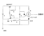
- FIG. 2 is a test circuit diagram of the current limiting circuit inductor of FIG. 1.
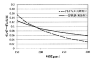
- FIG. 3 is an enlarged view of a graph showing the relationship between time and impedance when the current-limiting circuit inductor of FIG. 1 applied to the circuit of FIG. 2 is energized. It is a graph which shows the relationship between time when it supplies with electricity to the inductor for current limiting circuits of FIG. 1 applied to the circuit of FIG.
- FIG. 7B is a top view of the magnetic core of FIG. 7A. It is a graph of the test result which shows the impedance (Z / (alpha)) with respect to the shape factor (alpha) of each test body which has different shape factors (alpha) about the magnetic core of FIG. 7A and 7B.
- FIG. 2 is an explanatory diagram showing a magnetic path cross-sectional area and a magnetic path length in the magnetic core of the current limiting circuit inductor of FIG. 1.
- FIG. 11 is a graph showing the relationship between time and current when the current-limiting circuit inductor of FIG. 10 applied to the circuit of FIG. 2 is energized.
- 11 is a graph showing the relationship between time and impedance when the current-limiting circuit inductor of FIG. 10 applied to the circuit of FIG. 2 is energized.
- FIG. 11 is an enlarged view of a graph showing the relationship between time and impedance when the current-limiting circuit inductor of FIG. 10 applied to the circuit of FIG. 2 is energized.
- FIG. 11 is a graph showing the relationship between time and inductance when the current limiting circuit inductor of FIG. 10 applied to the circuit of FIG. 2 is energized. It is a graph of the test result which shows the impedance (Z / (alpha)) with respect to the shape factor (alpha) of each test body which has different shape count (alpha) about the magnetic core of the inductor for current limiting circuits which concerns on 4th Embodiment of this invention.
- the current limiting circuit inductor may be called a choke coil or a reactor.
- FIG. 1 is a perspective view showing a current-limiting circuit inductor according to a first embodiment of the present invention with a part thereof cut away.
- the current limiting circuit inductor 1 is a pot core type, and includes a so-called P-shaped magnetic core 2 and a cylindrical coil 3 built in the magnetic core 2.
- the coil 3 is composed of a conducting wire (not shown), and this conducting wire is wound coaxially with the central axis O of the magnetic core 2. Lead wires (not shown) are taken out from the magnetic core 2 from both ends of the conducting wire.
- the magnetic core 2 is divided into two divided bodies 2A and 2B by a dividing surface 4 orthogonal to the central axis O.
- the annular grooves 5A and 5B formed in each of the divided bodies 2A and 2B cooperate with each other to form a housing space for the coil 3.
- the divided bodies 2 ⁇ / b> A and 2 ⁇ / b> B are bonded by the dividing surface 4.
- a solventless epoxy adhesive, a silicone adhesive, or the like is used depending on the heat resistance required.
- the magnetic core 2 is made of a soft magnetic material having a low volume resistivity and a high magnetic permeability, and having a large iron loss at a high frequency unlike a general inductor. If it is such a soft magnetic material, the material is not particularly limited, but pure iron, which is a material having a low volume resistivity, a high magnetic permeability, and a high saturation magnetic flux density, is preferable. In particular, sintered pure iron obtained by compression-molding and sintering high-purity pure iron powder is preferable because of its low volume resistivity and high magnetic permeability. In that case, the density of sintered pure iron is preferably 7.4 ⁇ 10 3 kg / m 3 or more.
- the soft magnetic material may have a volume resistivity of 7.0 ⁇ 10 ⁇ 7 ⁇ ⁇ m or less and a maximum permeability of 2800 or more.
- the same soft magnetic material is used for the entire magnetic core 2, but only a part of the magnetic core 2, for example, a portion of the magnetic core 2 on the inner peripheral side or the outer peripheral side.
- a soft magnetic material may be used only for the portion, and a magnetic material of another material may be used for the remaining portion.
- a copper enameled wire is used as the conducting wire of the coil 3.
- urethane wire UEW
- formal wire PVF
- PET polyester wire
- EIW polyesterimide wire
- AIW polyamideimide wire
- PIW polyimide wire
- a round wire or a square wire can be used as the copper enamel wire.
- the coil 3 having improved winding density can be obtained by winding the short axis of the cross-sectional shape of the rectangular wire in contact with the periphery of the compression-molded magnetic body.
- the coil 3 is included in a resin molded body 6 that is a so-called insulating case.
- the resin material of the resin molded body 6 may be any resin material as long as it can fix the coil 3 and impart insulation.
- a thermoplastic resin that can be injection-molded is preferable. More preferred is polyphenylene sulfide (PPS).
- an epoxy resin used as a binder for the magnetic core 2 or a thermosetting resin such as a phenol resin can be used. It can also be set as the form of sealing.
- Example 1 In order to confirm the characteristics of the current limiting coil 1 according to the first embodiment, the following tests were performed.
- Example 1 the coil 3 is wound around a toroidal core made of sintered pure iron having a density of 7.4 ⁇ 10 3 kg / m 3 and having an outer diameter of 20.2 mm, an inner diameter of 12.6 mm, and a height of 6.4 mm.
- a test body made of an inductor was used.
- Comparative Example 1 a test body comprising an inductor having an amorphous dust core with a density of 5.7 ⁇ 10 3 kg / m 3 , and a coil 3 wound around a toroidal core of the same size as the toroidal core of Example 1.
- a powder-molded amorphous material was used as a material that is difficult to be magnetically saturated. Then, it was confirmed that the specimen of Example 1 was superior to the specimen of Comparative Example 1.
- Fig. 2 shows the test circuit.
- the capacitor C was charged by setting the switch SW to the position of the contact a.
- the switch SW was switched to the position of the contact b to finish charging the capacitor C, and an RLC circuit was formed to energize the specimen L1 (state of FIG. 2).
- the voltage of the power source V was 50 volts.
- An instantaneous large current was applied to each of the test bodies L1, and changes over time in the current and the terminal tube voltage of the inductor were measured.
- the test conditions were the same except that the magnetic cores of the test specimens were different.
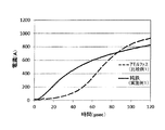
- FIG. 3 is a graph showing the relationship between the time during energization and the current of each specimen L1.
- the current limiting circuit inductor using amorphous in the magnetic core (hereinafter referred to as “amorphous current limiting inductor”), that is, the test body L1 of Comparative Example 1 has a large current suppressing effect when the current is small. As it increases, the current suppression effect decreases.
- the current-limiting circuit inductor of Example 1 hereinafter referred to as pure iron-based current limiting inductor
- pure iron-based current limiting inductor using sintered pure iron for the magnetic core has a small current suppressing effect at low current, and the current increases as the current increases. The suppression effect is increased.
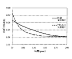
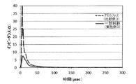
- FIGS. 4 and 5 are graphs showing the relationship between the time during energization and the impedance of each test specimen L1.
- the amorphous current-limiting inductor has a higher impedance immediately after energization than the pure iron-based current limiting inductor, but reverses with time (current increase).
- FIG. 6 is a graph showing the relationship between the time during energization and the inductance of each test specimen L1.
- An amorphous current-limiting inductor has a large inductance immediately after energization, but the inductance decreases with time (current increase).
- a pure iron-based current limiting inductor has an extremely small inductance immediately after energization, and the inductance increases with time.
- the current limiting circuit inductor of Example 1 has excellent inductance increasing characteristics when an instantaneous large current is applied.
- the current limiting circuit inductor 1 uses a magnetic core 2 made of sintered pure iron, which is a soft magnetic material having a low volume resistivity and a high magnetic permeability.
- the inductance increases as the current increases. For this reason, by providing the current limiting circuit having the current limiting circuit inductor 1 of this embodiment in series with the electric circuit to be protected, when an instantaneous current noise occurs, the electric circuit to be protected is greatly increased. It is possible to suppress the flow of current.
- the current limiting circuit inductor 1 since sintered pure iron is likely to have a high volume permeability with a low volume resistivity, the current limiting circuit inductor 1 has a characteristic that an inductance is extremely small at a low current. For this reason, it can be used as a low-inductance component at a normal current value. Therefore, the inductor according to the first embodiment is advantageous as the current-limiting circuit inductor 1 that desirably functions only during an abnormality. In addition, as described above, the current limiting circuit inductor 1 is likely to have a low volume resistivity and a high magnetic permeability, so that a large inductance can be obtained with a small physique.
- the manufacturing method of a sintered compact includes a compacting process and a subsequent sintering process. If the density of the green compact is about 6.8 or more, it can be an object of the sintering process, but if the density is lower than this, it cannot be handled due to insufficient strength. In addition, since the powder is pressed and hardened by compaction molding, since pores remain inside, it is impossible to manufacture a product close to the true density. At present, it is extremely difficult to produce a sintered body having a maximum of about 97% and a density exceeding 7.6 in practice.
- the soft magnetic material has a volume resistivity of 7.0 ⁇ 10 ⁇ 7 ⁇ ⁇ m or less and a maximum permeability of 2800 or more. Inductance can be obtained.
- the magnetic core 2 has a cylindrical shape in which the coil 3 is embedded.
- the second magnetic core 2 may be provided only on either the inner periphery or the outer periphery of the coil 3. .
- the magnetic core 2 is not limited to the pot type, and may be other various shapes of the magnetic core 2.
- the current-limiting circuit inductor according to the second embodiment includes a cylindrical magnetic core 2 shown in FIGS. 7A and 7B.
- the current-limiting circuit inductor having the magnetic core 2 of FIGS. 7A and 7B is the same as that of the first embodiment described above with reference to FIG.
- Example 2 (Execution / Comparative Example 2) 7A and 7B, how the ratio of the magnetic path cross-sectional area to the magnetic path length (magnetic path cross-sectional area / magnetic path length) influences the impedance using the magnetic core 2 formed of the toroidal core of the current-limiting circuit inductor. Tests were given to give. 7A and 7B, the cross section indicated by the symbol S is a cross section having a magnetic path cross-sectional area, and the circle indicated by the symbol 1 (indicated by a dotted line in FIG. 7B) is the circumference of the average diameter of the inner diameter and the outer diameter. And it consists of the line
- the test body is an inductor provided with a magnetic core 2 made of the above-mentioned toroidal core of sintered pure iron having a density of 7.70 g / cm 3 , and a test body L2 having a size shown in Table 3 below is prepared. No. 1 to No. 5).
- Test method An instantaneous large current was applied to the test body L2, and the time change of the current was measured.
- the test circuit during energization is the circuit shown in FIG.
- the capacitor C is charged with the switch SW of the figure connected to the contact b as shown in the figure, and the charging of the capacitor C is completed by switching the switch SW, and an electric current is supplied to the specimen by forming an RLC circuit. Energized.
- Table 4 shows the test results. Specifically, the relationship between the shape factor ⁇ and the ratio of the impedance Z to the shape factor ⁇ (hereinafter referred to as Z / ⁇ ) is shown in Table 4 and FIG.
- the shape factor ⁇ is a ratio of the magnetic path sectional area S to the magnetic path length l (magnetic path sectional area S / magnetic path length l).
- Z / ⁇ indicates an impedance that takes into account the shape factor ⁇ , and a larger value indicates closer to the ideal state and higher efficiency. The smaller the peak current, the larger the impedance obtained from the current and voltage, and the impedance was efficiently obtained when the shape factor ⁇ was 0.9 or more.
- the impedance changes according to the magnetic path cross-sectional area / magnetic path length, and when this ratio is 0.9 or more, the impedance can be obtained efficiently.
- the above test is a test on the toroidal type magnetic core shown in FIGS. 7A and 7B, but it is estimated that the same result is obtained even in the case of the pot core type magnetic core 2 shown in FIG.
- the magnetic path cross-sectional area and magnetic path length of the magnetic core 2 are the area and length shown in FIG.
- the magnetic path cross-sectional area includes the first cross-sectional area S1 of the cross section 2aa of the outer portion of the magnetic core 2, the second cross-sectional area S2 of the cross section 2bb of the inner portion of the magnetic core 2, and the upper portion of the magnetic core 2. Is the average of the third cross-sectional area S3 of the cross-section 2cc and the fourth cross-sectional area S4 of the cross-section 2dd of the lower portion of the magnetic core 2.
- the third cross-sectional area S3 and the fourth cross-sectional area S4 of the cross-sections 2cc and 2dd of the upper part and the lower part of the magnetic core 2 respectively correspond to the inner part of the magnetic core 2 at the heights d1 and d2 of the respective parts. Is multiplied by the circumference of the average diameter ((r2-r1) / 2) of the outer diameter r1 of the magnetic core 2 and the inner diameter r2 of the outer portion of the magnetic core 2.
- the magnetic path length l is obtained based on a path along the center of each magnetic path cross section.
- the point that the magnetic path cross-sectional area / magnetic path length is preferably 0.9 or more applies regardless of the shape of the magnetic core.
- FIG. 10 is a perspective view of an inductor for a current limiting circuit according to the third embodiment of the present invention.
- This inductor 1A for current limiting circuit has a hollow cylindrical magnetic core 2 which is a toroidal core type, and two windings 3A and 3B wound around the magnetic core 2. Since it has two windings 3A and 3B, the current limiting circuit inductor 1A is a four-terminal type. These two windings 3A and 3B are used in a current limiting circuit as a common mode coil.
- Each of the windings 3A and 3B is wound around the outer periphery of the cross section of the magnetic core 2 having a hollow cylindrical shape, and the winding directions are opposite to each other.
- Both end portions of each of the windings 3A and 3B serve as lead wires, and both ends of these windings 3A and 3B constitute terminals 3Aa, 3Ab, 3Ba, and 3Bb, respectively.
- Each winding 3A, 3B may be wound around the magnetic core 2 via a coil bobbin (not shown).
- the winding of each winding may be bifilar winding.
- FIG. 11 is a diagram showing only the magnetic core 2.
- the illustrated magnetic core 2 has a two-layer structure including an inner peripheral portion 4 and an outer peripheral portion 5 having a uniform thickness.
- a soft magnetic material having a low volume resistivity and a high magnetic permeability and a large iron loss at high frequency is used.
- the material is not particularly limited, but an iron-based sintered metal (for example, pure iron or low carbon) having a low volume resistivity, a high magnetic permeability, and a high saturation magnetic flux density.
- an iron-based sintered metal for example, pure iron or low carbon
- steel a metal mainly composed of iron such as SKD11
- sintered pure iron obtained by compression-molding and sintering high-purity pure iron powder is more preferable because of its low volume resistivity and high magnetic permeability.
- the density of sintered pure iron is preferably 7.4 g / cm 3 or more.
- the soft magnetic material may have a volume resistivity of 7.0 ⁇ 10 ⁇ 7 ⁇ ⁇ m or less and a maximum permeability of 2800 or more.
- the outer peripheral portion 5 is a so-called dust core using an amorphous powder, and is formed by annealing a compression-molded amorphous alloy powder that has been treated with an insulating coating.
- the magnetic core 2 has a structure in which the inner and outer parts 4 are made of the above-described soft magnetic material instead of the inner peripheral part 4 as in the third embodiment.
- a soft magnetic material may be used, and the dust core made of the amorphous alloy powder may be used for the inner peripheral portion 4.
- the soft magnetic material is made of the same material, and has the above-described low volume resistivity, high magnetic permeability, and high iron loss at high frequencies. It may be used.
- the windings 3A and 3B of the coil 3 have the same characteristics as the coil 3 of the inductor 1 according to the first embodiment.
- Example 3 In order to confirm the characteristics of the inductor for current limiting circuit according to the third embodiment, the following test was performed.
- Example 3 and Comparative Example 3 As the test body L3 of Example 3 of the inductor included in the third embodiment, the inner peripheral portion 4 shown in FIG. 11 is made of an iron-based material (SKD11), and the other portion 5 is made of an amorphous alloy powder.
- an inductor including a magnetic core which is a pot core having the same shape and dimensions as the test body of Example 3 and having an entire amorphous structure, was prepared as the test body L3 serving as Comparative Example 3.
- a common-mode air-core coil with the same specifications was set on these cores to form test specimens.
- an amorphous pot-type core was used as a material that hardly resists magnetic saturation in the inner peripheral portion 4 shown in FIG.
- test circuit As the test circuit, the test circuit of FIG. 2 used in Example 1, Comparative Example 1, and Example / Comparative Example 2 was used.
- FIG. 12 is a graph showing the relationship between the time during energization and the current of each specimen L3.
- the current limiting circuit inductor (hereinafter referred to as “amorphous current limiting inductor”) using only the dust core using amorphous alloy powder in the magnetic core, that is, the test body L3 of Comparative Example 3 has a large current suppressing effect when the current is small. However, the current suppression effect decreases as the current increases.
- the test body L3 of No. 3 has a small current suppression effect at a low current, and the current suppression effect increases as the current increases.
- FIGS. 13 and 14 are graphs showing the relationship between the time during energization and the impedance of each specimen L3.
- Amorphous current-limiting inductors have higher impedance immediately after energization than some pure iron-based current limiting inductors, but reverse with time (current increase).
- FIG. 15 is a graph showing the relationship between the time during energization and the inductance of each test specimen L3.
- An amorphous current-limiting inductor has a large inductance immediately after energization, but the inductance decreases with time (current increase).
- some of the pure iron-based current limiting inductors have extremely small inductance at a low current immediately after energization, and the inductance increases as the current value increases with time.
- the current limiting circuit inductor of Example 3 has an increased inductance when an instantaneous large current is applied. Excellent characteristics.
- the current limiting circuit inductor 1A of the third embodiment uses sintered pure iron, which is a soft magnetic material having a low volume resistivity and a high magnetic permeability, in at least a part of the magnetic core 2.
- sintered pure iron which is a soft magnetic material having a low volume resistivity and a high magnetic permeability, in at least a part of the magnetic core 2.
- the characteristics are opposite to those of a conventional current limiting coil using ferrite in the magnetic core, and the inductance increases as the current increases.
- the target electric circuit is generated when instantaneous current noise occurs. It is possible to limit the flow of a large current in
- Sintered pure iron tends to have a low volume resistivity and a high magnetic permeability, but this current limiting circuit inductor 1A has a characteristic that the inductance is extremely small at a low current. Therefore, it can be used as a low-inductance component at a normal current value. Therefore, the inductor according to the third embodiment is advantageous as an inductor for a current-limiting circuit that is desired to function only at the time of abnormality.
- the current limiting circuit inductor 1 is likely to have a low volume resistivity and a high magnetic permeability, so that a large inductance can be obtained with a small physique.
- the soft magnetic material has a volume resistivity of 7.0 ⁇ 10 ⁇ 7 ⁇ ⁇ m or less and a maximum magnetic permeability of 2800 or more. Inductance can be obtained.
- the relationship of the current limiting effect with respect to the volume low efficiency and the magnetic permeability is the relationship of Table 2 shown regarding the first embodiment.
- Examplementation / Comparative Example 4 As the magnetic core 2, the same one as in the above-mentioned implementation / comparative example 2 is used, and, similarly to the above-mentioned implementation / comparative example 2, a test is conducted to determine how the magnetic path cross-sectional area / magnetic path length affects the impedance. went.
- As the magnetic core 2 of the test body one having the same size as shown in Table 3 and the same as the above-described Example 2 was prepared. Bifilar windings (double windings) were performed on these magnetic cores 2, and the specimens L4 (No. 1 to No. 5) shown in Table 3 were obtained in the same manner as in Example 2 and Comparative Example.
- Test method was also the same method as in the implementation / comparative example 2.
- the test results are shown in Table 5. Specifically, the relationship between the shape factor ⁇ and the ratio of the impedance Z to the shape factor ⁇ (hereinafter referred to as the shape factor ⁇ ) is shown in Table 5 and FIG.
- the shape factor ⁇ is a ratio of the magnetic path sectional area S to the magnetic path length l (magnetic path sectional area S / magnetic path length l).
- Z / ⁇ indicates an impedance that takes into account the shape factor ⁇ , and a larger value indicates closer to the ideal state and higher efficiency. The smaller the peak current, the larger the impedance obtained from the current and voltage, and the impedance was efficiently obtained when the shape factor ⁇ was 0.9 or more.
- the impedance changes according to the magnetic path cross-sectional area / magnetic path length, and when this ratio is 0.9 or more, the impedance can be obtained efficiently.
- the magnetic core 2 has a cylindrical shape in which the windings 3A and 3B are wound around the outer periphery.
- the magnetic core 2 may have a shape provided only on either the inner periphery or the outer periphery of the coil 3. good.
- Various shapes can be adopted for the magnetic core 2.
Landscapes
- Engineering & Computer Science (AREA)
- Power Engineering (AREA)
- Coils Or Transformers For Communication (AREA)
Abstract
小さなサイズでありながら、瞬時の大電流通電時に大きなインダクタンスを保持し、電流を制限する効果を発揮できる限流回路用インダクタを提供する。特に、通常運転時はインダクタンスを必要としない電気回路にこの限流回路用インダクタは適する。この限流回路用インダクタ(1)は、磁心(2)と、コイル(3)とを備え、限流回路に用いられる。磁心(2)は、その少なくとも一部に、低体積抵抗率かつ高透磁率の軟磁性材料からなる部分を有する。軟磁性材料は、例えば焼結製純鉄である。
Description
本出願は、2015年5月28日出願の特願2015-108370および特願2015-108371ならびに2015年11月5日出願の特願2015-217456および特願2015-217512の優先権を主張するものであり、その全体を参照により本願の一部をなすものとして引用する。
この発明は、漏電発生時もしくはブレーカ動作時、または落雷等により発生する瞬時の大電流ノイズに対する対策として電流の突入速度を低減するためのインダクタとして用いられる限流回路用のインダクタであって、特に通常運転時にはインダクタとして機能しない事が望ましい限流回路用インダクタに関する。
種々の電気設備、例えば、太陽光発電や風力発電用のコンバータ、およびデータセンターの電気設備では、大出力化に伴い大電力を扱う用途が拡大してきている。これら電気設備の機器では大電力を扱うことから、高度な安全対策が求められることもある。そのため、これら機器は高価である場合多い。また、近年ではサージ電流と呼ばれる、雷等の瞬時の大電流ノイズに対する安全面の対策として、装置の保護対策が重要になってきている。
漏電発生時もしくはブレーカ動作時、または落雷等により発生する瞬間的な電流ノイズは、対象回路の定格電流の数倍以上の大電流になる場合が多い。回路への大電流の突入を防止するために回路上に直列にインダクタを設ける場合がある。
なお、遮断装置において、限流装置を設けることがある(例えば、特許文献1)。
なお、遮断装置において、限流装置を設けることがある(例えば、特許文献1)。
従来の瞬間的な電流ノイズの対策として用いられるインダクタは、いずれも、大電流により磁気飽和させないために、大きいサイズを有する。
サージ電流に代表される様な、電流変化速度が速くかつ極めて大きな電流がインダクタに流れると、磁心の磁気飽和に伴う透磁率の低下によりインダクタンスが減少し電流の抑制効果(インピーダンス)が小さくなる。インダクタを磁気飽和させないためには、用いる磁心のサイズを非常に大きくし、大電流により発生する磁束密度を十分小さく抑える必要がある。なお、この明細書で言う「インダクタンス」とは、磁心形状とコイルの巻き数および磁心の材料特性に準ずる透磁率により決まるインダクタの重要特性である。インダクタンス値が大きいほどインダクタのインピーダンスが大きくなることから、インダクタンス値が大きいほどインダクタに流れる電流変化速度は小さく、電流抑制効果は大きい。
この発明は、上記課題を解消するものであり、瞬時の大電流通電時に、小さな体格のインダクタでありながら大きなインダクタンスならびにインピーダンスを保持し電流の抑制効果を発揮することができる限流回路用インダクタを提供することを目的とする。
この発明の一構成に係る限流回路用インダクタは、磁心と、この磁心に巻回された導線からなるコイルとを備え、限流回路に用いられるインダクタであって、前記磁心は、その少なくとも一部に、低体積抵抗率かつ高透磁率の軟磁性材料からなる部分を有する。前記軟磁性材料は、好ましくは、高周波時の鉄損が大きい軟磁性材である。
本発明者は、軸心の少なくとも一部を上記材質の軟磁性材料にすることで、電流が増加するにつれてインダクタンスが大きくなる従来のインダクタ特性とは逆の特性となることを見いだした。この特性は、従来のインダクタの特性とは異なり、瞬時の大電流通電時でも、大きなインピーダンスを保持できることから、小さな体格のインダクタで、大きな電流の抑制効果を発揮できる。なお、通常運転時に通電される電流は、本インダクタが機能すべき大電流と比べると十分小さいことから、通常運転時には、本構成のインダクタは低いインダクタンスとなる。また大電流ノイズと比べると通常運転時の電流は、直流や50Hz程度の低周波数の交流の場合が多いことから、電流変化速度も小さく、低インピーダンスとなる。したがって、本構成のインダクタは、異常時のみ機能する限流回路用インダクタとして望ましい。
なお、限流回路用インダクタは、「限流コイル」とも呼ばれる。前記「低体積抵抗率」とは、フェライトに較べて体積抵抗率が低いものを言う。また、前記「高透磁率」とは最大透磁率が1000以上のものを言う。
好ましい実施形態において、前記コイルは、前記磁心に互いに逆向きに導線を巻いた少なくとも2個のコイルからなり、これら2個のコイルはコモンモードコイルとして用いられる。
上述したインダクタ特性により、瞬時の大電流に対して磁気飽和することなく大きなインピーダンスを保持できることから、電流の突入速度を低減することができる。
好ましい実施形態において、前記磁心の全体が前記軟磁性材料であっても良い。磁心の全体に前記材質の軟磁性材料を用いれば、瞬時の大電流通電時でも、小さな体格のインダクタで、大きなインダクタンスおよびインピーダンスを保持し電流の抑制効果を発揮することができるという利点が得られる。
好ましい実施形態において、前記軟磁性材料が焼結製純鉄であっても良い。前記磁心に用いる材料として、低体積抵抗率でかつ高透磁率の軟磁性材料であれば、特に材質の限定はないが、体積抵抗率が低くかつ高透磁率で飽和磁束密度も大きい材料としては、純鉄が好ましい。特に、低体積抵抗率で高透磁率となり易いことから、高純度純鉄粉を圧縮成形し焼結させた焼結製高純度純鉄がより好ましい。
さらに好ましい実施形態において、前記焼結製純鉄の密度が7.4×10³kg/m3(=7.4g/cm3)以上であることが好ましい。前記焼結製純鉄の密度が7.4×103kg/m3以上であると、試験の結果、瞬時の大電流の通電時においてインダクタンスが増大することが確認された。
好ましい実施形態において、前記軟磁性材料は、体積抵抗率が7.0×10⁻⁷Ω・m以下で、かつ最大透磁率が2800以上である。このように体積抵抗率が小さく、最大透磁率が大きいと、瞬時の大電流通電時でも、小さな体格のインダクタで、大きなインダクタンスおよびインピーダンスを保持し電流の抑制効果を発揮することができると言う利点が、より一層効果的に得られる。
好ましい実施形態において、前記磁心の磁路断面積/磁路長の比が0.9以上であっても良い。試験によると、磁路断面積/磁路長の比によってインピーダンスが変わり、前記の比が0.9以上である場合に、効率良くインピーダンスが得られた。
請求の範囲および/または明細書および/または図面に開示された少なくとも2つの構成のどのような組合せも、本発明に含まれる。特に、請求の範囲の各請求項の2つ以上のどのような組合せも、本発明に含まれる。
この発明は、添付の図面を参考にした以下の好適な実施形態の説明から、より明瞭に理解されるであろう。しかしながら、実施形態および図面は単なる図示および説明のためのものであり、この発明の範囲を定めるために利用されるべきものではない。この発明の範囲は添付の請求の範囲によって定まる。添付図面において、複数の図面における同一の符号は、同一または相当する部分を示す。
この発明の第1の実施形態にかかる限流回路用インダクタの一部分を切り離して表した断面斜視図である。
図1の限流回路用インダクタの試験回路図である。
図2の回路に適用した図1の限流回路用インダクタに通電したときの時間と電流との関係を示すグラフである。
図2の回路に適用した図1の限流回路用インダクタに通電したときの時間とインピーダンスとの関係を示すグラフである。
図2の回路に適用した図1の限流回路用インダクタに通電したときの時間とインピーダンスとの関係を示すグラフの拡大図である。
図2の回路に適用した図1の限流回路用インダクタに通電したときの時間とインダクタンスとの関係を示すグラフである。
この発明の第2の実施形態における限流回路用インダクタの磁心であって、試験体として用いた磁心の斜視図である。
図7Aの磁心の上面図である。
図7Aおよび7Bの磁心につき、異なる形状係数αを有する各試験体の、形状係数αに対するインピーダンス(Z/α)を示す試験結果のグラフである。
図1の限流回路用インダクタの磁心における、磁路断面積および磁路長を示す説明図である。
この発明の第3の実施形態にかかる限流回路用インダクタの斜視図である。
図10の限流回路用インダクタの磁心の斜視図である。
図2の回路に適用した図10の限流回路用インダクタに通電したときの時間と電流との関係を示すグラフである。
図2の回路に適用した図10の限流回路用インダクタに通電したときの時間とインピーダンスとの関係を示すグラフである。
図2の回路に適用した図10の限流回路用インダクタに通電したときの時間とインピーダンスとの関係を示すグラフの拡大図である。
図2の回路に適用した図10の限流回路用インダクタに通電したときの時間とインダクタンスとの関係を示すグラフである。
この発明の第4の実施形態に係る限流回路用インダクタの磁心につき、異なる形状計数αを有する各試験体の、形状係数αに対するインピーダンス(Z/α)を示す試験結果のグラフである。
この発明の第1の実施形態に係る限流回路用インダクタを図面と共に説明する。なお、この限流回路用インダクタは、チョークコイルまたはリアクトルと呼ばれることがある。
図1は、この発明の第1の実施形態にかかる限流回路用インダクタを、一部分を切り離して表わした斜視図である。この限流回路用インダクタ1は、ポットコア型であって、所謂P形の磁心2と、この磁心2に内蔵された円筒形のコイル3とを備える。コイル3は、導線(図示せず)からなり、この導線は、磁心2の中心軸Oと同軸で巻回されている。導線の両端から引き出し線(図示せず)が磁心2の外に取り出されている。
磁心2は、中心軸Oと直交する分割面4により2つの分割体2A,2Bに分割される。各分割体2A,2Bにそれぞれ形成された環状溝5A,5Bが互いに協働してコイル3の収容空間を構成する。分割状態にある磁心2の収容空間にコイル3を収容した後、分割体2A,2Bを分割面4で接着する。接着には、例えば無溶剤型のエポキシ系接着材やシリコーン系接着剤等が要求される耐熱性等に応じて用いられる。
前記磁心2には、低体積抵抗率で、かつ高透磁率で、さらに一般的なインダクタとは異なり高周波時の鉄損が大きい軟磁性材料が使用される。このような軟磁性材料であれば、特に材質は限定されないが、体積抵抗率が低く、かつ高透磁率で、飽和磁束密度も大きい材質である、純鉄が好ましい。特に、低体積抵抗率で高透磁率となり易いことから、高純度の純鉄粉を圧縮成形し焼結させた焼結製純鉄が好ましい。その場合、焼結製純鉄の密度が7.4×10³kg/m3以上であるのが良い。また、軟磁性材料は、体積抵抗率が7.0×10-7Ω・m以下で、かつ最大透磁率が2800以上であるのが良い。
この第1の実施形態では、磁心2の全体に同じ材質の軟磁性材料を使用したが、磁心2の一部にだけ、例えば磁心2におけるコイル3よりも内周側の部分、または外周側の部分だけに軟磁性材料を使用し、残り部分には他の材質の磁性材料を使用しても良い。
前記コイル3の導線としては、例えば銅エナメル線が用いられる。詳しくは、ウレタン線(UEW)、ホルマール線(PVF)、ポリエステル線(PEW)、ポリエステルイミド線(EIW)、ポリアミドイミド線(AIW)、ポリイミド線(PIW)、これらを組み合わせた二重被覆線、または自己融着線、リッツ線等を使用できる。銅エナメル線としては、丸線や角線を使用できる。特に、平角線の断面形状の短径側を圧縮成形磁性体の周囲に接して重ね巻きすることにより、巻線密度を向上させたコイル3が得られる。
コイル3は、この第1の実施形態では所謂絶縁ケースとなる樹脂成形体6に内包された形態としている。樹脂成形体6の樹脂材としては、コイル3を固定し、絶縁性を付与できるものであればいかなる樹脂材であってもよい。ただし、好ましくは、射出成形が可能な熱可塑性樹脂である。さらに好ましくは、ポリフェニレンサルファイド(PPS)である。
コイル3を内包する樹脂成形体6の樹脂材としては、上記熱可塑性樹脂以外に、磁心2の結着材として使用されるエポキシ樹脂、またはフェノール樹脂等の熱硬化性樹脂も使用でき、所謂樹脂封止の形態とすることもできる。
この第1の実施形態に係る限流コイル1の特性を確かめるために、以下の試験を行った。
(実施例1および比較例1)
実施例1において、密度が7.4×10³kg/m3の焼結製純鉄からなる外径20.2mm、内径12.6mm、高さ6.4mmのトロイダルコアにコイル3を巻線したインダクタからなる試験体を用いた。また、比較例1として、密度が5.7×103kg/m3のアモルファスダストコアからなり、実施例1のトロイダルコアと同一サイズのトロイダルコアにコイル3を巻線したインダクタからなる試験体を用いた。この比較例1には、磁気飽和し難い材料として、圧粉成形アモルファスを用いた。その上で、実施例1の試験体が比較例1の試験体よりも優れていることを確認した。
(実施例1および比較例1)
実施例1において、密度が7.4×10³kg/m3の焼結製純鉄からなる外径20.2mm、内径12.6mm、高さ6.4mmのトロイダルコアにコイル3を巻線したインダクタからなる試験体を用いた。また、比較例1として、密度が5.7×103kg/m3のアモルファスダストコアからなり、実施例1のトロイダルコアと同一サイズのトロイダルコアにコイル3を巻線したインダクタからなる試験体を用いた。この比較例1には、磁気飽和し難い材料として、圧粉成形アモルファスを用いた。その上で、実施例1の試験体が比較例1の試験体よりも優れていることを確認した。
図2は試験回路を示す。始めに、スイッチSWを接点aの位置にして、コンデンサCを充電した。次に、スイッチSWを接点bの位置に切り換えて、コンデンサCへの充電を終了すると共に、RLC回路を形成して試験体L1に通電した(図2の状態)。電源Vの電圧は50ボルトとした。前記各試験体L1に瞬時の大電流を通電し、電流およびインダクタの端子管電圧の時間変化を測定した。なお、試験において各試験体の磁心が異なる以外は同条件とした。
図3は、通電時における時間と前記各試験体L1の電流との関係を示すグラフである。磁心にアモルファスを使用した限流回路用インダクタ(以下、「アモルファス系限流インダクタ」と称する)つまり比較例1の試験体L1は、電流が小さいときは大きな電流抑制効果が得られるが、電流が増加するのに伴い電流抑制効果が減少する。これに対し、磁心に焼結製純鉄を使用した実施例1の限流回路用インダクタ(以下、純鉄系限流インダクタ)は、低電流時に電流抑制効果が小さく、電流が増加するにつれ電流抑制効果が大きくなる。
図4および5は、通電時における時間と前記各試験体L1のインピーダンスとの関係を示すグラフである。アモルファス系限流インダクタは、純鉄系限流インダクタに較べ通電直後は高いインピーダンスであるが、時間経過(電流の増加)に伴い逆転する。
図6は、通電時における時間と前記各試験体L1のインダクタンスとの関係を示すグラフである。アモルファス系限流インダクタは、通電直後は大きなインダクタンスであるが、時間経過(電流の増加)に伴いインダクタンスが減少する。これに対し、純鉄系限流インダクタは、通電直後はインダクタンスが極めて小さく、時間経過に伴いインダクタンスが大きくなる。
磁気飽和し難いアモルファスを磁心に使用した限流回路用インダクタと比較しても、実施例1の限流回路用インダクタは、瞬時の大電流を通電時におけるインダクタンスの増大特性が優れている。
このように、この第1の実施形態の限流回路用インダクタ1は、磁心2に低体積抵抗率で、かつ高透磁率の軟磁性材料である焼結製純鉄を使用することで、磁心にフェライトを用いた従来の限流回路用インダクタとは逆の特性となり、電流が増加するにつれてインダクタンスが大きくなる。このため、保護対象とする電気回路と直列にこの実施形態の限流回路用インダクタ1を有する限流回路を設けることにより、瞬間的な電流ノイズが発生した場合に、対象とする電気回路に大電流が流れるのを抑制することができる。
また、焼結製純鉄は低体積抵抗率で高透磁率となり易いため、この限流回路用インダクタ1は、低電流時はインダクタンスが極めて小さいという特性を持つ。このため、通常の電流値では低インダクタンス部品として利用することができる。したがって、この第1の実施形態に係るインダクタは、異常時のみ機能することが望ましい限流回路用インダクタ1として有利である。また、上記のように、この限流回路用インダクタ1は、低体積抵抗率で高透磁率となり易いため、小さな体格で大きなインダクタンスが得られる。
なお、上記試験例では、焼結製純鉄の密度が7.4×10³kg/m3の焼結純鉄を用いたが、密度が7.4×103kg/m3よりも大きい焼結製純鉄を用いると、より一層、低体積抵抗率で高透磁率となる。

ここで、焼結体の製造方法は、圧粉成形工程と、これに続く焼結工程とを含む。圧粉成形体の密度が6.8程度以上あれば焼結工程の対象になり得るが、これよりも低密度の場合、強度不足で取り扱えなくなる。また圧粉成形で粉を押し固めて製造することから、空孔が内部に残るため、真密度に近いものは製造不可能である。現時点では最大で97%程度で、実際には密度7.6を超える焼結体を製造することは極めて困難である。
また、この第1の実施形態では、軟磁性材料は、体積抵抗率が7.0×10⁻⁷Ω・m以下で、かつ最大透磁率が2800以上であるため、小さな体格のインダクタで、大きなインダクタンスを得ることができる。
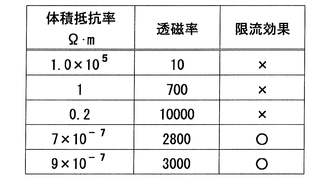
なお、上記第1の実施形態では、磁心2を、内部にコイル3を埋め込む円筒形としたが、第2の磁心2は、コイル3の内周または外周のいずれか一方のみに設けても良い。磁心2はまた、ポット型に限らず、他の種々の形状の磁心2であっても良い。第2の実施形態に係る限流回路用インダクタは、図7Aおよび7Bに示す円筒形の磁心2を備える。図7Aおよび7Bの磁心2を有する限流回路用インダクタは、特に説明する事項を除き、図1と共に前述した第1の実施形態と同様である。
他の試験例につき説明する。
(実施・比較例2)
図7Aおよび7Bの限流回路用インダクタのトロイダルコアからなる磁心2を用いて、磁路長に対する磁路断面積の比(磁路断面積/磁路長)が、インピーダンスにどのような影響を与えるかにつき試験を行った。図7Aおよび7Bにおいて、符号Sで示す断面は、磁路断面積を有する断面であり、符号l(図7Bにて点線にて表記)で示す円は、内径と外径の平均径の円周であって、磁路長を成す線からなる。
(実施・比較例2)
図7Aおよび7Bの限流回路用インダクタのトロイダルコアからなる磁心2を用いて、磁路長に対する磁路断面積の比(磁路断面積/磁路長)が、インピーダンスにどのような影響を与えるかにつき試験を行った。図7Aおよび7Bにおいて、符号Sで示す断面は、磁路断面積を有する断面であり、符号l(図7Bにて点線にて表記)で示す円は、内径と外径の平均径の円周であって、磁路長を成す線からなる。
試験体は、密度7.70g/cm3の焼結系純鉄の上記トロイダルコアからなる磁心2を備えたインダクタであって、次の表3に示すサイズのものを用意し、試験体L2(No.1~No.5)とした。
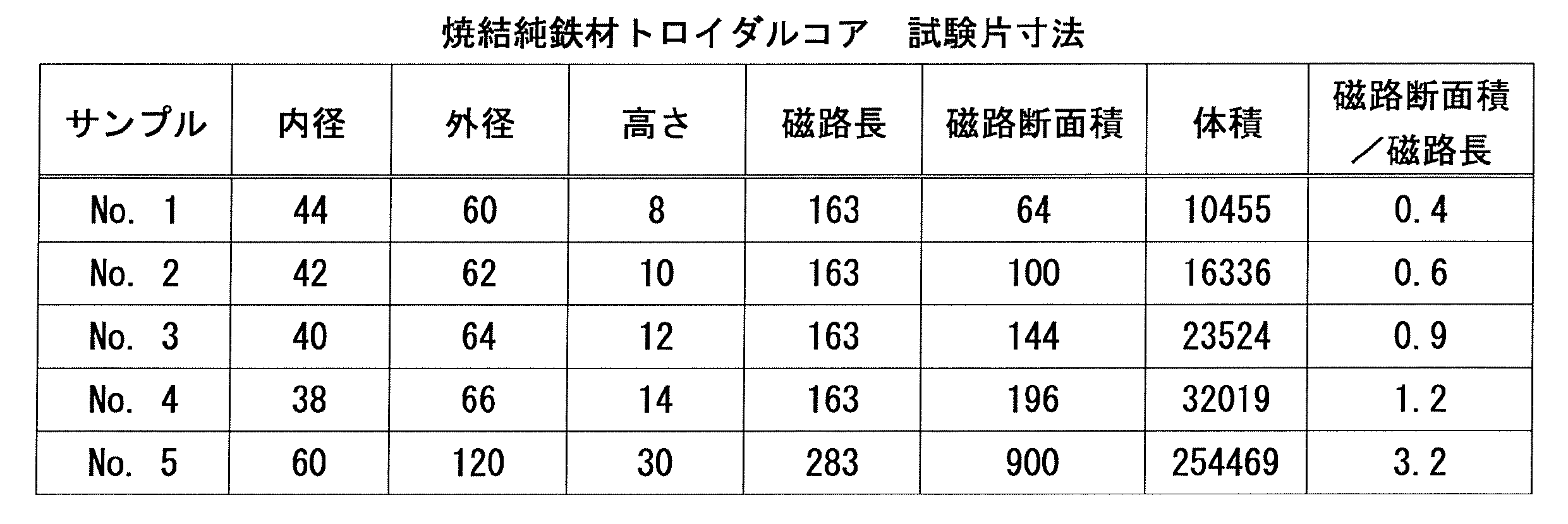
(試験方法)
試験体L2に瞬時の大電流を通電し、電流の時間変化を測定した。
通電時の試験回路は、前述した図2に示す回路である。同図のスイッチSWを同図のように接点bに接続した状態でコンデンサCを充電し、スイッチSWの切り替えによってコンデンサCの充電を終了すると共に、RLC回路を形成することで試験体に電流を通電した。
試験体L2に瞬時の大電流を通電し、電流の時間変化を測定した。
通電時の試験回路は、前述した図2に示す回路である。同図のスイッチSWを同図のように接点bに接続した状態でコンデンサCを充電し、スイッチSWの切り替えによってコンデンサCの充電を終了すると共に、RLC回路を形成することで試験体に電流を通電した。
試験の結果を表4に示す。具体的には、形状係数αと、形状係数αに対するインピーダンスZの比(以下、Z/αとする)との関係を表4および図8に示す。なお、形状係数αは、磁路長lに対する磁路断面積Sの比(磁路断面積S/磁路長l)である。
Z/αは、形状係数αを加味したインピーダンスを示し、大きい値ほど理想状態に近く、効率の良いことを示す。ピーク電流の小さいものほど、電流と電圧より求めたインピーダンスが大きく、形状係数αが0.9以上のときに、効率よくインピーダンスが得られていた。
Z/αは、形状係数αを加味したインピーダンスを示し、大きい値ほど理想状態に近く、効率の良いことを示す。ピーク電流の小さいものほど、電流と電圧より求めたインピーダンスが大きく、形状係数αが0.9以上のときに、効率よくインピーダンスが得られていた。

上記試験の結果からわかるように、磁路断面積/磁路長に従ってインピーダンスが変わり、この比が0.9以上である場合に、効率良くインピーダンスが得られる。
なお、前記試験は、図7Aおよび7Bに示すトロイダル型の磁心における試験であるが、図1に示すポットコア型の磁心2であっても、同様の結果であると推測される。
なお、前記試験は、図7Aおよび7Bに示すトロイダル型の磁心における試験であるが、図1に示すポットコア型の磁心2であっても、同様の結果であると推測される。
図1の実施形態における限流回路用インダクタの場合、その磁心2の磁路断面積および磁路長は、図9に示す面積および長さとなる。具体的には、磁路断面積は、磁心2の外側部分の断面2aaの第1の断面積S1と、磁心2の内側部分の断面2bbの第2の断面積S2と、磁心2の上側部分の断面2ccの第3の断面積S3と、磁心2の下側部分の断面2ddの第4の断面積S4との平均である。なお、磁心2の上側部分および下側部分それぞれの断面2cc,2ddの各第3の断面積S3および第4の断面積S4は、各部分の高さd1およびd2それぞれに、磁心2の内側部分の外径r1と、磁心2の外側部分の内径r2との平均径((r2-r1)/2)についての周長を乗じて求められる。磁路断面積を求める式は、以下のとおりとなる。
S=(S1+S2+S3+S4)/4
S=(S1+S2+S3+S4)/4
磁路長lは、各磁路断面の中央に沿った経路に基づいて求められる。
磁路断面積/磁路長が0.9以上であるのが好ましい点は、磁心の形状に関わらずに当てはまる。
次に、この発明の第3の実施形態に係る限流回路用インダクタを図面と共に説明する。なお、本実施形態において、第1の実施形態に関して説明した構成要素と共通する構成要素については、同一の参照符号を付して説明を省略する。
図10は、この発明の第3の実施形態にかかる限流回路用インダクタの斜視図である。この限流回路用インダクタ1Aは、トロイダルコア型である中空の円筒形の磁心2と、この磁心2に巻き付けられた2本の巻線3A,3Bとを有する。2本巻線3A,3Bを有するため、この限流回路用インダクタ1Aは4端子型である。これら2本巻線3A,3Bは、コモンモードコイルとして限流回路に用いられる。各巻線3A,3Bは、中空円筒形である磁心2の断面の外周に巻回されており、それぞれの巻き方向は互いに逆向きである。各巻線3A,3Bの両端部は、それぞれ引出し線とされ、これら巻線3A,3Bの両方の先端がそれぞれ端子3Aa,3Ab,3Ba,3Bbを構成する。各巻線3A,3Bは、コイルボビン(図示せず)を介して磁心2に巻付けられていても良い。各巻線の巻き方はバイファイラ巻きであっても良い。
図11は、磁心2だけを示す図である。図示の磁心2は、均一厚さの内周部分4と、外周部分5とから構成される2層構造である。
内周部分4には、低体積抵抗率および高透磁率で、かつ高周波時の鉄損が大きい軟磁性材料が使用される。このような軟磁性材料であれば、特に材質は限定されないが、体積抵抗率が低く、かつ高透磁率で、飽和磁束密度も大きい材質である、鉄系焼結金属(例えば純鉄や低炭素鋼、SKD11等の鉄分を主成分とする金属)が好ましい。特に、低体積抵抗率で高透磁率となり易いことから、高純度の純鉄粉を圧縮成形し焼結させた焼結製純鉄がより好ましい。その場合、焼結製純鉄の密度が7.4g/cm3以上であるのが良い。また、軟磁性材料は、体積抵抗率が7.0×10-7Ω・m以下で、かつ最大透磁率が2800以上であるのが良い。
外周部分5は、アモルファス粉末を用いた所謂ダストコアであり、絶縁被膜処理されたアモルファス合金粉末を圧縮成形したものを焼鈍して作られている。
なお、磁心2は、この第3の実施形態のように内周部分4に前記材質の軟磁性材料を使用した構成に代えて、内外の材質を互いに逆に、つまり外周部分5に前記材質の軟磁性材料を用い、内周部分4に前記アモルファス合金粉製のダストコアを用いても良い。また、第2の実施形態に関して説明した図7Aおよび7Bの磁心2のように全体を同じ材質とし、前述した低体積抵抗率、高透磁率で、かつ高周波時の鉄損が大きい軟磁性材料を用いても良い。
前記コイル3の巻線3A,3Bは、第1の実施形態に係るインダクタ1のコイル3と同様の特徴を有する。
この第3の実施形態に係る限流回路用インダクタの特性を確かめるために、次の試験を行った。
(実施例3および比較例3)
試験体には、第3の実施形態に含まれるインダクタの実施例3の試験体L3として、図11に示す内周部分4が鉄系材料(SKD11)で、他の部分5がアモルファス合金粉末に樹脂バインダを用いて射出成形により成形したポット型コア(外径120mm、内径28mm、高さ93mm)である磁心を含むインダクタを用意した。また、比較例3となる試験体L3として、実施例3の試験体と同形同寸法で全体がアモルファスのポット型コアである磁心を含むインダクタを用意した。これらのコアに同じ仕様のコモンモードの空心コイルをセットしてそれぞれ試験体とした。前記比較例3には、図11に示す内周部分4に磁気飽和し難い材料として、アモルファスのポット型コアを用いた。その上で、実施例3の試験体が比較例3の試験体よりも優れていることを確認した。
(実施例3および比較例3)
試験体には、第3の実施形態に含まれるインダクタの実施例3の試験体L3として、図11に示す内周部分4が鉄系材料(SKD11)で、他の部分5がアモルファス合金粉末に樹脂バインダを用いて射出成形により成形したポット型コア(外径120mm、内径28mm、高さ93mm)である磁心を含むインダクタを用意した。また、比較例3となる試験体L3として、実施例3の試験体と同形同寸法で全体がアモルファスのポット型コアである磁心を含むインダクタを用意した。これらのコアに同じ仕様のコモンモードの空心コイルをセットしてそれぞれ試験体とした。前記比較例3には、図11に示す内周部分4に磁気飽和し難い材料として、アモルファスのポット型コアを用いた。その上で、実施例3の試験体が比較例3の試験体よりも優れていることを確認した。
試験回路としては、実施例1、比較例1および実施・比較例2で用いた図2の試験回路を用いた。
図12は、通電時における時間と前記各試験体L3の電流との関係を示すグラフである。磁心にアモルファス合金粉末を用いたダストコアのみを使用した限流回路用インダクタ(以下、「アモルファス系限流インダクタ」と称する)つまり比較例3の試験体L3は、電流が小さいときは大きな電流抑制効果が得られるが、電流が増加するのに伴い電流抑制効果が減少する。これに対し、図11の内周部分が鉄系材料、他の部分がアモルファス系合金粉末を用いたダストコアを使用した限流回路用インダクタ(以下、一部純鉄系限流インダクタ)つまり実施例3の試験体L3は、低電流時に電流抑制効果が小さく、電流が増加するにつれ電流抑制効果が大きくなる。
図13および14は、通電時における時間と前記各試験体L3のインピーダンスとの関係を示すグラフである。アモルファス系限流インダクタは、一部純鉄系限流インダクタに較べ通電直後は高いインピーダンスであるが、時間経過(電流の増加)に伴い逆転する。
図15は、通電時における時間と前記各試験体L3のインダクタンスとの関係を示すグラフである。アモルファス系限流インダクタは、通電直後は大きなインダクタンスであるが、時間経過(電流の増加)に伴いインダクタンスが減少する。これに対し、一部純鉄系限流インダクタは、通電直後の低電流時はインダクタンスが極めて小さく、時間経過に伴い電流値が大きくなるとインダクタンスが大きくなる。
磁気飽和し難い磁心にアモルファス合金粉末を用いたダストコアのみを使用した限流回路用インダクタと比較しても、実施例3の限流回路用インダクタは、瞬時の大電流を通電時におけるインダクタンスの増大特性が優れている。
このように、この第3の実施形態の限流回路用インダクタ1Aは、磁心2の少なくとも一部に低体積抵抗率で、かつ高透磁率の軟磁性材料である焼結製純鉄を使用することで、磁心にフェライトを用いた従来の限流コイルとは逆の特性となり、電流が増加するにつれてインダクタンスが大きくなる。このため、対象とする電気回路と直列にこの第3の実施形態の限流回路用インダクタ1Aを有する限流回路を設けることにより、瞬間的な電流ノイズが発生した場合に、対象とする電気回路に大電流が流れるのを制限することができる。
また、焼結製純鉄は低体積抵抗率で高透磁率となり易いが、この限流回路用インダクタ1Aは、低電流時はインダクタンスが極めて小さいという特性を持つ。したがって、通常の電流値では低インダクタンス部品として利用することができる。そのため、この第3の実施形態に係るインダクタは、異常時のみ機能することが望まれる限流回路用インダクタとして有利である。また、上記のように、この限流回路用インダクタ1は、低体積抵抗率で高透磁率となり易いため、小さな体格で大きなインダクタンスが得られる。
なお、この第3の実施形態では、軟磁性材料は、体積抵抗率が7.0×10⁻⁷Ω・m以下で、かつ最大透磁率が2800以上であるため、小さな体格のインダクタで、大きなインダクタンスを得ることができる。なお、体積低効率および透磁率に対する限流効果の関係は、第1実施形態に関して示した表2の関係が当てはまる。
他の試験例につき説明する。
(実施・比較例4)
磁心2としては、上記実施・比較例2と同一のものを用い、上記実施・比較例2と同様に、磁路断面積/磁路長が、インピーダンスにどのような影響を与えるかにつき試験を行った。試験体の磁心2として、上記実施・比較例2と同一で、表3で示したサイズのものを用意した。これら磁心2に、バイファイラ巻線(2重巻線)を行い、上記実施・比較例2と同一で、表3で示した試験体L4(No.1~No.5)とした。
(実施・比較例4)
磁心2としては、上記実施・比較例2と同一のものを用い、上記実施・比較例2と同様に、磁路断面積/磁路長が、インピーダンスにどのような影響を与えるかにつき試験を行った。試験体の磁心2として、上記実施・比較例2と同一で、表3で示したサイズのものを用意した。これら磁心2に、バイファイラ巻線(2重巻線)を行い、上記実施・比較例2と同一で、表3で示した試験体L4(No.1~No.5)とした。
(削除)
(試験方法)
試験方法も、実施・比較例2と同一の方法であった。
試験方法も、実施・比較例2と同一の方法であった。
試験の結果を表5に示す。具体的には、形状係数αと、形状係数αに対するインピーダンスZの比(以下、形状係数αとする)との関係を表5および図16に示す。なお、形状係数αは、磁路長lに対する磁路断面積Sの比(磁路断面積S/磁路長l)である。
Z/αは、形状係数αを加味したインピーダンスを示し、大きい値ほど理想状態に近く、効率の良いことを示す。ピーク電流の小さいものほど、電流と電圧より求めたインピーダンスが大きく、形状係数αが0.9以上のときに、効率よくインピーダンスが得られていた。
Z/αは、形状係数αを加味したインピーダンスを示し、大きい値ほど理想状態に近く、効率の良いことを示す。ピーク電流の小さいものほど、電流と電圧より求めたインピーダンスが大きく、形状係数αが0.9以上のときに、効率よくインピーダンスが得られていた。

上記試験の結果からわかるように、磁路断面積/磁路長に従ってインピーダンスが変わり、この比が0.9以上である場合に、効率良くインピーダンスが得られる。
なお、上記各実施形態では、磁心2を、外周に巻線3A,3Bを巻く円筒形としたが、磁心2は、コイル3の内周または外周のいずれか一方のみに設ける形状であっても良い。磁心2には、また、種々の形状を採用することができる。
以上、実施例に基づいて本発明を実施するための形態を説明したが、ここで開示した実施の形態はすべての点で例示であって制限的なものではない。本発明の範囲は上記した説明ではなくて特許請求の範囲によって示され、特許請求の範囲と均等の意味および範囲内でのすべての変更が含まれることが意図される。
1(1A) 限流回路用インダクタ
2 磁心
3(3A,3B) コイル
2 磁心
3(3A,3B) コイル
Claims (7)
- 磁心と、コイルとを備え、限流回路に用いられるインダクタであって、
前記磁心は、その少なくとも一部に、低体積抵抗率かつ高透磁率の軟磁性材料からなる部分を有する限流回路用インダクタ。 - 請求項1に記載の限流回路用インダクタにおいて、
前記コイルは、前記磁心に導線を互いに逆向きに巻いた少なくとも2個のコイルからなり、これら2個のコイルはコモンモードコイルとして用いられる、限流回路用インダクタ。 - 請求項1または2に記載の限流回路用インダクタにおいて、前記磁心の全体が前記軟磁性材料である限流回路用インダクタ。
- 請求項1ないし請求項3に記載の限流回路用インダクタにおいて、前記軟磁性材料が焼結製純鉄である限流回路用インダクタ。
- 請求項4に記載の限流回路用インダクタにおいて、前記焼結製純鉄の密度が7.4×10³kg/m3以上である限流回路用インダクタ。
- 請求項1ないし請求項5のいずれか1項に記載の限流回路用インダクタにおいて、前記軟磁性材料は、体積抵抗率が7.0×10⁻⁷Ω・m以下で、かつ最大透磁率が2800以上である限流回路用インダクタ。
- 請求項1ないし請求項6のいずれか1項に記載の限流回路用インダクタにおいて、前記磁心の磁路断面積/磁路長の比が0.9以上である限流回路用インダクタ。
Applications Claiming Priority (8)
| Application Number | Priority Date | Filing Date | Title |
|---|---|---|---|
| JP2015108371 | 2015-05-28 | ||
| JP2015108370 | 2015-05-28 | ||
| JP2015-108371 | 2015-05-28 | ||
| JP2015-108370 | 2015-05-28 | ||
| JP2015-217512 | 2015-11-05 | ||
| JP2015217456A JP2016225589A (ja) | 2015-05-28 | 2015-11-05 | 限流回路用インダクタ |
| JP2015-217456 | 2015-11-05 | ||
| JP2015217512A JP2016225590A (ja) | 2015-05-28 | 2015-11-05 | 限流回路用インダクタ |
Publications (1)
| Publication Number | Publication Date |
|---|---|
| WO2016190319A1 true WO2016190319A1 (ja) | 2016-12-01 |
Family
ID=57392938
Family Applications (1)
| Application Number | Title | Priority Date | Filing Date |
|---|---|---|---|
| PCT/JP2016/065343 Ceased WO2016190319A1 (ja) | 2015-05-28 | 2016-05-24 | 限流回路用インダクタ |
Country Status (1)
| Country | Link |
|---|---|
| WO (1) | WO2016190319A1 (ja) |
Citations (4)
| Publication number | Priority date | Publication date | Assignee | Title |
|---|---|---|---|---|
| JPH1066254A (ja) * | 1996-08-09 | 1998-03-06 | Tokyo Electric Power Co Inc:The | 放電装置付き限流リアクトルとその制御方式 |
| JP2001238349A (ja) * | 2000-02-25 | 2001-08-31 | Mitsubishi Electric Corp | 限流器 |
| JP2006197667A (ja) * | 2005-01-11 | 2006-07-27 | Mitsubishi Electric Corp | 限流器 |
| JP2013532909A (ja) * | 2010-08-03 | 2013-08-19 | アルストム テクノロジー リミテッド | コア |
-
2016
- 2016-05-24 WO PCT/JP2016/065343 patent/WO2016190319A1/ja not_active Ceased
Patent Citations (4)
| Publication number | Priority date | Publication date | Assignee | Title |
|---|---|---|---|---|
| JPH1066254A (ja) * | 1996-08-09 | 1998-03-06 | Tokyo Electric Power Co Inc:The | 放電装置付き限流リアクトルとその制御方式 |
| JP2001238349A (ja) * | 2000-02-25 | 2001-08-31 | Mitsubishi Electric Corp | 限流器 |
| JP2006197667A (ja) * | 2005-01-11 | 2006-07-27 | Mitsubishi Electric Corp | 限流器 |
| JP2013532909A (ja) * | 2010-08-03 | 2013-08-19 | アルストム テクノロジー リミテッド | コア |
Similar Documents
| Publication | Publication Date | Title |
|---|---|---|
| JP6826794B2 (ja) | 薄型高電流対応複合体の変圧器 | |
| CN100458988C (zh) | 扼流线圈及其内埋型铁芯 | |
| CN107430930A (zh) | 电感器以及保护电路 | |
| CN103493157B (zh) | 线缆及包括其的电磁设备 | |
| JP3614816B2 (ja) | 磁性素子およびそれを用いた電源 | |
| JP2013501369A (ja) | 電流補償チョークおよび電流補償チョークの製造方法 | |
| JP2016058495A (ja) | コモンモードチョークコイル、コモンモードフィルタ、および電力変換装置 | |
| CN111415810A (zh) | 一种差共模一体扼流圈 | |
| CN103680849A (zh) | 表面安装电感器 | |
| TWI622067B (zh) | Coil component | |
| JP2016039322A (ja) | コイル、及びコイル部品 | |
| JP2016225590A (ja) | 限流回路用インダクタ | |
| JP6776793B2 (ja) | コイル部品 | |
| JP2012204454A (ja) | インダクタ及び2相インターリーブ制御方式力率改善コンバータ | |
| JP5079316B2 (ja) | インダクタンス素子 | |
| WO2016190319A1 (ja) | 限流回路用インダクタ | |
| JP2016225589A (ja) | 限流回路用インダクタ | |
| KR20160099208A (ko) | 코일 부품, 이를 포함하는 대전류 인덕터 및 대전류 리액터 | |
| JP2016063158A (ja) | インダクタ | |
| JP2018056396A (ja) | コイル部品 | |
| JP2003282342A (ja) | コイル封入圧粉磁芯 | |
| JP4300494B2 (ja) | 高周波パワートランスおよびこれを用いた電力変換装置 | |
| JP2006294733A (ja) | インダクタ及びその製造方法 | |
| US20240258008A1 (en) | Common mode choke, winding method for common mode choke, and adapter | |
| US9583255B2 (en) | Surge blocking inductor |
Legal Events
| Date | Code | Title | Description |
|---|---|---|---|
| 121 | Ep: the epo has been informed by wipo that ep was designated in this application |
Ref document number: 16800024 Country of ref document: EP Kind code of ref document: A1 |
|
| NENP | Non-entry into the national phase |
Ref country code: DE |
|
| 122 | Ep: pct application non-entry in european phase |
Ref document number: 16800024 Country of ref document: EP Kind code of ref document: A1 |