WO2016189597A1 - 表示装置 - Google Patents
表示装置 Download PDFInfo
- Publication number
- WO2016189597A1 WO2016189597A1 PCT/JP2015/064801 JP2015064801W WO2016189597A1 WO 2016189597 A1 WO2016189597 A1 WO 2016189597A1 JP 2015064801 W JP2015064801 W JP 2015064801W WO 2016189597 A1 WO2016189597 A1 WO 2016189597A1
- Authority
- WO
- WIPO (PCT)
- Prior art keywords
- input
- video
- video signal
- scanning signal
- signal line
- Prior art date
- Legal status (The legal status is an assumption and is not a legal conclusion. Google has not performed a legal analysis and makes no representation as to the accuracy of the status listed.)
- Ceased
Links
Images



Classifications
-
- G—PHYSICS
- G09—EDUCATION; CRYPTOGRAPHY; DISPLAY; ADVERTISING; SEALS
- G09G—ARRANGEMENTS OR CIRCUITS FOR CONTROL OF INDICATING DEVICES USING STATIC MEANS TO PRESENT VARIABLE INFORMATION
- G09G3/00—Control arrangements or circuits, of interest only in connection with visual indicators other than cathode-ray tubes
- G09G3/20—Control arrangements or circuits, of interest only in connection with visual indicators other than cathode-ray tubes for presentation of an assembly of a number of characters, e.g. a page, by composing the assembly by combination of individual elements arranged in a matrix no fixed position being assigned to or needed to be assigned to the individual characters or partial characters
-
- G—PHYSICS
- G09—EDUCATION; CRYPTOGRAPHY; DISPLAY; ADVERTISING; SEALS
- G09G—ARRANGEMENTS OR CIRCUITS FOR CONTROL OF INDICATING DEVICES USING STATIC MEANS TO PRESENT VARIABLE INFORMATION
- G09G3/00—Control arrangements or circuits, of interest only in connection with visual indicators other than cathode-ray tubes
- G09G3/20—Control arrangements or circuits, of interest only in connection with visual indicators other than cathode-ray tubes for presentation of an assembly of a number of characters, e.g. a page, by composing the assembly by combination of individual elements arranged in a matrix no fixed position being assigned to or needed to be assigned to the individual characters or partial characters
- G09G3/34—Control arrangements or circuits, of interest only in connection with visual indicators other than cathode-ray tubes for presentation of an assembly of a number of characters, e.g. a page, by composing the assembly by combination of individual elements arranged in a matrix no fixed position being assigned to or needed to be assigned to the individual characters or partial characters by control of light from an independent source
- G09G3/36—Control arrangements or circuits, of interest only in connection with visual indicators other than cathode-ray tubes for presentation of an assembly of a number of characters, e.g. a page, by composing the assembly by combination of individual elements arranged in a matrix no fixed position being assigned to or needed to be assigned to the individual characters or partial characters by control of light from an independent source using liquid crystals
Definitions
- the present invention relates to a display device that displays video.
- the display device includes a display panel and a video drive unit.
- the display panel includes a plurality of video signal lines and scanning signal lines arranged in a vertical and horizontal grid pattern, and pixel electrodes arranged one by one corresponding to the intersections of the video signal lines and the scanning signal lines. Included (see Patent Document 1).
- the video driver is connected to the end of the video signal line. Scan signals are input to the scan signal lines in order from the closest to the video drive unit.
- the video driver inputs video signals to all video signal lines when a scanning signal is input to any of the scanning signal lines.
- the video signal is given to the pixel electrode arranged corresponding to the scanning signal line to which the scanning signal is input.
- the video displayed on the display panel includes pixels having gradation values corresponding to the video signal applied to the pixel electrodes.
- the gradation value of the image pixel actually displayed by the display device may be different from the gradation value of the image pixel that the display device should have originally displayed.
- display quality is deteriorated such that a checkered image with an unnecessary stripe pattern is displayed.
- the gradation value possessed by the pixel of the video to be originally displayed is referred to as the input gradation value
- the gradation value possessed by the pixel of the image displayed by the display device is referred to as the output gradation value.
- a pixel electrode corresponding to a target pixel (a pixel to be image-processed) is referred to as a target pixel electrode.
- a pixel electrode adjacent to the side closer to the pixel is referred to as a pre-stage pixel electrode.
- the pre-stage pixel electrode is a pixel electrode adjacent to the target pixel electrode in the vertical direction (length direction of the video signal line).
- the front stage pixel is a pixel corresponding to the front stage pixel electrode.
- the reason for the deterioration in display quality described above is that the input tone value of the target pixel is adversely affected by the input tone value of the previous pixel. This is because the video driver outputs the video signal output from the video signal corresponding to the input gradation value of the previous pixel (previous video signal) to the video signal corresponding to the input gradation value of the target pixel (target video signal). This is because the previous video signal is still flowing through the video signal line immediately after switching the video signal.
- the video signal flowing through the video signal line changes from the previous video signal to a video signal in which the previous video signal and the target video signal are superimposed, and eventually converges to the target video signal.
- the video signal is a rectangular wave signal
- waveform rounding may occur due to superposition with the preceding video signal.
- the difference between the output gradation value of the target pixel and the input gradation value of the target pixel tends to become more serious as the target pixel electrode is farther from the video driver. This is because, as the distance from the video drive unit increases, adverse effects such as electrical resistance and capacitance of the video signal line affect the video signal, and the rise time of the video signal is unnecessarily prolonged (that is, the waveform rounding is worsened). It is.
- the display device described in Patent Document 1 by delaying the timing at which the scanning signal is input to the scanning signal line from the conventional timing, the time during which the focused video signal with the waveform rounding is given to the focused pixel electrode is reduced. Shorten. However, the display device described in Patent Document 1 does not consider the problem that the waveform rounding worsens as the pixel electrode of interest is farther from the video driving unit.
- the present invention has been made in view of such circumstances, and a main object thereof is to provide a display device capable of improving display quality.
- the display device includes a plurality of video signal lines, a plurality of scanning signal lines that are juxtaposed so as to intersect the plurality of video signal lines, and sequentially connected to the video signal lines.
- a plurality of pixel electrodes that are connected to end portions of the plurality of video signal lines, and when a scanning signal is input to the scanning signal line, a video signal applied to the pixel electrode is converted to the video signal.
- the scanning signal is input to the scanning signal line
- the timing at which the video signal is input to the video signal line with respect to the time point differs according to the distance from the video input unit of the scanning signal line to which the scanning signal is input.
- one video input unit inputs a video signal from one end of the video signal line, and the scanning signal line arranged at a position close to the video input unit.
- the timing at which the video signal is input to the video signal line based on the time when the scanning signal is input is a scanning signal line arranged at a position far from the video input unit.
- the timing is later than the timing at which the video signal is input to the video signal line based on the time when the scanning signal is input.
- the display device is configured such that the two video input units input video signals from both ends of the video signal line, and are arranged at a position close to one of the two video input units.
- the scanning signal is input to the scanning signal line
- the timing at which the video signal is input to the video signal line with reference to the time when the scanning signal is input is from both of the two video input units.
- the timing is later than the timing at which the video signal is input to the video signal line based on the time point when the scanning signal is input
- the display device further includes a temperature detection unit, and when the detection result of the temperature detection unit is high temperature, the timing at which the video signal is input is delayed compared to the case where the detection result is low temperature. It is made to do so.
- the timing at which the video signal is applied to the pixel electrode near the video input unit, and the video input unit is different.
- the amplitude of the video signal needs to correspond to the input gradation value, but when the waveform is rounded in the video signal, the amplitude of the video signal is smaller (or larger) than the amplitude A corresponding to the input gradation value. ) Become amplitude. However, the amplitude of the video signal in which the waveform is rounded converges to the amplitude A over time. Therefore, if a video signal having a large waveform round is applied to the pixel electrode early and a video signal having a small waveform round is applied to the pixel electrode later, a video signal having an amplitude A is applied to each pixel electrode for a necessary and sufficient time. As a result, a pixel having a gradation value corresponding to the input gradation value is displayed.
- the present invention there is a high possibility that waveform rounding hardly occurs in the video signal applied to the pixel electrode close to the video input unit. Therefore, if the video signal is given to the pixel electrode near the video input unit for a relatively short time, the video signal having the amplitude A can be given for a necessary and sufficient time. As a result, a pixel having a gradation value (that is, an input gradation value) corresponding to the amplitude A of the video signal can be displayed without any problem.
- the timing at which the video signal is input to the video signal line is advanced (or delayed). This is because, for example, the response speed of the liquid crystal contained in the liquid crystal display panel is slower as the temperature is lower (or faster as the temperature is higher). As a result, the adverse effect of temperature can be eliminated and display quality can be improved.
- the timing for applying the video signal to the pixel electrode is changed according to the distance from the video input unit of the pixel electrode. Therefore, the video signal in which the waveform rounding is converged is given to the pixel electrode for a necessary and sufficient time. Therefore, not only the waveform rounding caused by the difference between the target input tone value and the previous input tone value but also the adverse effect of the waveform rounding caused by the distance from the video input unit can be eliminated, and the display quality can be improved. it can.
- FIG. 1 is a block diagram showing a configuration of a display device 2 according to Embodiment 1 of the present invention.
- 2 is a block diagram showing a connection relationship between the pixel electrodes 14, 14,... Included in the display device 2 and the video signal lines 11, 11,... And the scanning signal lines 12, 12,.
- FIG. 3 is a block diagram illustrating a configuration of a control system of the display device 2.
- the display device 2 of the present embodiment is configured as a television receiver or a display of a personal computer.
- the display device 2 displays a full-color image using, for example, RGB (Red, Green, Blue) three primary colors.
- the display device 2 is not limited to the three primary colors RGB, but may be the four primary colors RGBY (Red, Green, Blue, Yellow) or the four primary colors RGBW (Red, Green, Blue, White).
- the display device 2 includes a liquid crystal display panel 1, K video drive units 21, 21,... (Video input unit), L scan drive units 22, 22,.
- K and L there are a plurality of K and L.
- the display device 2 includes one video driving unit 21 and one scanning driving unit 22.
- the vertical and horizontal directions of the liquid crystal display panel 1 are the vertical and horizontal directions as viewed in the figure.
- the liquid crystal display panel 1 includes two light-transmitting substrates disposed facing each other in the front-rear direction, and liquid crystal sealed between the light-transmitting substrates (each illustrated).
- M video signal lines 11, 11,..., N scanning signal lines 12, 12,..., ⁇ M ⁇ N ⁇ TFTs 13, 13,. And ⁇ M ⁇ N ⁇ pixel electrodes 14, 14,... are provided on one side of the transparent substrate.
- a transparent electrode layer (not shown) is provided on the other side of the translucent substrate.
- FIG. 2 in order to distinguish the video signal lines 11, 11,... And the scanning signal lines 12, 12,. L2, ... are attached.
- FIG. 2 in order to distinguish the TFTs 13, 13,... And the pixel electrodes 14, 14,. ... is attached.
- the TFT 13 is represented by a letter “T”.
- the image displayed on the liquid crystal display panel 1 includes pixels corresponding to the pixel electrodes 14, 14. Each pixel has an output gradation value of R color, G color, or B color. The output gradation value of each pixel corresponds to the amplitude of the video signal applied to the pixel electrode 14 corresponding to the pixel. 2 and 3, the pixel electrode 14 corresponding to the R (or G or B) pixel is represented by the letter “R” (or “G” or “B”).
- R or G or B
- the output gradation value of each pixel included in the image is equal to the input gradation value of each pixel included in the image to be originally displayed.
- Each gradation value is an integer from “0” to “255”.
- the video signal lines 11, 11,... are juxtaposed at an appropriate distance in the left-right direction (the width direction of the liquid crystal display panel 1).
- Each video signal line 11 is long in the vertical direction (the height direction of the liquid crystal display panel 1).
- the video signal lines 11 L1 , 11 L2 ,... are arranged in this order from the left.
- the scanning signal lines 12, 12,... are juxtaposed at an appropriate distance in the vertical direction.
- Each scanning signal line 12 is long in the left-right direction, and crosses the M video signal lines 11, 11,. In other words, the video signal lines 11, 11,... And the scanning signal lines 12, 12,.
- the scanning signal lines 12 L1 , 12 L2 ,... are arranged in this order from the top.
- the TFTs 13, 13,... are arranged in the vicinity of the intersections one by one corresponding to the intersections of the video signal lines 11, 11,.
- Each TFT 13 is a switching element and is connected to the video signal line 11 and the scanning signal line 12 at the intersection.
- the source electrode (and gate electrode) of the TFT 13 is connected to the video signal line 11 (and scanning signal line 12).
- TFTs 13 11 , 13 12 ,... (And TFTs 13 21 , 13 22 ,...) Are arranged in this order from above and connected to the video signal line 11 L1 (and video signal line 11 L2 ). Yes.
- the TFTs 13 11 , 13 12 ,... are individually connected to the scanning signal lines 12 L1 , 12 L2,.
- the TFTs 13 21 , 13 22 are individually connected to the scanning signal lines 12 L1 , 12 L2,.
- the pixel electrodes 14, 14,... are arranged in a matrix and are connected to the drain electrodes of the TFTs 13, 13,. That is, the pixel electrode 14 is connected to the video signal line 11 through the TFT 13.
- the TFT 13 is not shown for simplification of the drawing. Accordingly, the pixel electrode 14 shown in FIG. 3 is depicted as if it were directly connected to the video signal line 11 and the scanning signal line 12.
- the video drive unit 21 is connected to the upper ends of the video signal lines 11, 11,.
- a plurality of later-described gradation signals are sequentially input to the video driving unit 21, and a later-described latch strobe signal (“LS” in FIG. 3) is input at an appropriate timing.
- a video signal, a gradation signal, and a latch strobe signal, and a gate clock (“GC” in FIG. 3) and a scanning signal, which will be described later, are respectively rectangular wave signals.
- the latch strobe signal indicates the timing at which the video drive unit 21 outputs the video signal. Each time the latch strobe signal is input, the video drive unit 21 outputs M video signals to the M video signal lines 11, 11,. The M video signals output at this time correspond to the most recent M gray level signals among the gray level signals input to the video drive unit 21.
- the gradation signal indicates the gradation value.
- the video signal corresponding to the gradation signal has an amplitude corresponding to the gradation value indicated by the gradation signal.
- the output of the video signal to each video signal line 11 is continued until at least the next latch strobe signal is input after the latch strobe signal is input. That is, every time the latch strobe signal is input, the video driver 21 changes the amplitude of the video signal to be output or maintains the same amplitude.
- each pixel electrode 14 from the video drive unit 21 is from the video drive unit 21 of the scanning signal line 12 corresponding to the pixel electrode 14 (that is, the scanning signal line 12 connected to the pixel electrode 14 via the TFT 13). Corresponding to the perspective. The closer the scanning signal line 12 corresponding to the pixel electrode 14 is to the upper side (that is, the closer the scanning signal line 12 is to the video driving unit 21), the closer the pixel electrode 14 is to the video driving unit 21.
- the scanning drive unit 22 is connected to the left end of the scanning signal lines 12, 12,.
- a gate clock is intermittently input to the scan driver 22 at a fixed timing.
- the gate clock indicates the timing at which the scan driver 22 outputs a scan signal.
- the scanning drive unit 22 continues to output the scanning signal to any one scanning signal line 12 for a predetermined time H after the gate clock is input, and when the predetermined time H has passed, the scanning driving unit 22 supplies the scanning signal to the scanning signal line 12.
- the output of the scanning signal is stopped.
- the scanning signal input to the scanning signal line 12 is applied to the TFTs 13, 13,... Connected to the scanning signal line 12 to which the scanning signal is input.
- the TFT 13 is normally turned off, and is turned on only while the scanning signal is applied (that is, for a predetermined time H).
- a video signal is given to the pixel electrodes 14, 14,... Connected to the TFTs 13, 13,. .. Are not supplied to the pixel electrodes 14, 14,... Connected to the TFTs 13, 13,.
- a video signal is applied to the pixel electrode 14
- a voltage corresponding to the amplitude of the applied video signal is applied between the pixel electrode 14 that has received the video signal and the above-described transparent electrode layer.
- the orientation of the liquid crystal existing between the pixel electrode 14 receiving the video signal and the transparent electrode layer changes.
- the gradation value of the pixel corresponding to the pixel electrode 14 that has received the video signal becomes a gradation value corresponding to the amplitude of the video signal.
- the scan driver 22 sequentially outputs the scan signals from the scan signal line 12 on the upper side (side closer to the video driver 21). Specifically, when the scanning drive unit 22 outputs a scanning signal to the scanning signal line 12 L1 with the input of the gate clock, the scanning driving unit 22 outputs the scanning signal to the scanning signal line 12 L2 with the input of the next gate clock. To do.
- the previous pixel electrode corresponding to the previous pixel is the pixel electrode 14 11 (or pixel electrode 14 21 ).
- the previous pixel electrode corresponding to the previous pixel is the pixel electrode 14 12 (or pixel electrode 14 22 ).
- the scanning driver 22 outputs the scanning signal to the scanning signal line 12 at the uppermost position.
- a plurality of gradation signals are sequentially input to the control unit 23.
- the control unit 23 sequentially outputs the input gradation signals to the video driving unit 21.
- the control unit 23 controls the operations of the video drive unit 21 and the scan drive unit 22.
- the control unit 23 outputs the gate clock to the scan driving unit one by one at a constant cycle.
- One gate clock is output every time M gradation signals are output.
- the control unit 23 outputs a latch strobe signal to the video drive unit 21 at an appropriate timing.
- One latch strobe signal is output each time one gate clock is output.
- the gradation signal input to the control unit 23 receives a television broadcast wave from the outside via an antenna (not shown), converts the received television broadcast wave into a broadcast signal, and converts the received broadcast broadcast signal into a predetermined broadcast signal. Signal processing is performed. That is, the gradation value indicated by the gradation signal is an input gradation value.
- the gradation signal input to the control unit 23 may be obtained by appropriately correcting the input gradation value. This correction desirably includes a correction for suppressing the difference between the input gradation value and the output gradation value.
- the timing at which the video signal is input to the video signal lines 11, 11,... Based on the time when the scanning signal is input to the scanning signal line 12 is constant.
- t T (T is a constant of T ⁇ 0).
- the timing at which the video signal is input to the video signal lines 11, 11,... Based on the time when the scanning signal is input to the scanning signal line 12 is the scanning signal line 12 to which the scanning signal is input.
- the distance from the image drive unit 21 that is, the distance from the image drive unit 21 to the pixel electrodes 14, 14,... To which the image signal is applied).
- the timing at which the scanning signal is input to the scanning signal line 12 corresponds to the timing at which the gate clock is input to the scanning drive unit 22, and the timing at which the video signal is input to the video signal lines 11, 11,. This corresponds to the timing at which the latch strobe signal is input to the unit 21.
- the timing at which the gate clock is input to the scan driver 22 corresponds to the timing at which the gate clock is output from the controller 23 to the scan driver 22, and the timing at which the latch strobe signal is input to the video driver 21 is controlled. This corresponds to the timing at which the video signal is output from the unit 23 to the video signal lines 11, 11,. That is, the elapsed time t corresponds to the elapsed time from when the gate clock is output to the scan driver 22 until the video signal is output to the video signal lines 11, 11.
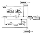
- FIG. 4 is a block diagram illustrating a configuration of the control unit 23.
- the control unit 23 includes a column counter 231, a row counter 232, a time table 233, and a calculation unit 234.
- the gradation signal input to the control unit 23 is given to the column counter 231 and the calculation unit 234.
- individual row numbers are assigned to the scanning signal lines 12, 12,.
- the row numbers assigned to the scanning signal lines 12, 12,... Are “1”, “2”,.
- the scanning signal line 12 with the larger row number is farther from the video driver 21.
- the count result of the column counter 231 before displaying the video is reset to “0”.
- the column counter 231 increments the count result by “1” every time a gradation signal is given.
- the column counter 231 gives a predetermined count signal to the row counter 232 and resets the count result to “0”.
- the count result of the row counter 232 before displaying the video is reset to “1”.
- the row counter 232 increments the count result by “1” every time the count signal is given.
- the row counter 232 resets the count result to “1”.
- the coefficient result of the row counter 232 is the row number of the scanning signal line 12 to which the pixel electrode 14 corresponding to the target pixel is connected via the TFT 13.
- the time table 233 is a data table stored in a nonvolatile memory (not shown).
- the row number and the elapsed time t are stored in association with each other. The larger the line number, the smaller the associated elapsed time t.
- the time table 233 stores first to third elapsed times t.
- the number of elapsed time t stored in the time table 233 may be two or four or more. However, when the number of elapsed times t is excessive (for example, a different elapsed time t is set for each row number), not only the setting process of the elapsed time t becomes complicated, but also the time table 233 is stored. A non-volatile memory having an excessive storage capacity is required.
- the calculation unit 234 outputs the given gradation signal to the video driving unit 21 as it is every time the gradation signal is given. In addition, the calculation unit 234 acquires a count result (that is, a row number) from the row counter 232. Next, the computing unit 234 refers to the time table 233 using the acquired line number and obtains the elapsed time t. Further, the calculation unit 234 outputs a gate clock to the scan driving unit 22 at a predetermined timing, and starts measuring the elapsed time from the output time of the gate clock.
- the calculation unit 234 waits for the output of the latch strobe signal until the time measurement result reaches the elapsed time t, and outputs the latch strobe signal to the video drive unit 21 when the time measurement result is equal to or longer than the elapsed time t. Finally, the calculation unit 234 ends the elapsed time measurement and resets the time measurement result to “0”.
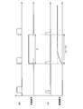
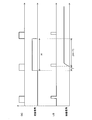
- FIG. 5 and 6 are timing charts showing the output timings of the gate clock, the scanning signal, the latch strobe signal, and the video signal in the display device 2, respectively.
- FIG. 5 shows a case where the scanning signal line 12 is close to the video driving unit 21, and
- FIG. 6 shows a case where the scanning signal line 12 is far from the video driving unit 21.
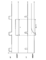
- 7 and 8 are timing charts showing the output timings of the gate clock, the scanning signal, the latch strobe signal, and the video signal in the conventional display device. 7 and 8 correspond to FIGS. 5 and 6. 7 and 8 illustrate the case where T> 0.
- FIG. 5 and 7 show gradations from the same video signal line 11 to the pixel electrodes 14, 14, 14 corresponding to the scanning signal lines 12, 12, 12 of the row numbers “1”, “2”, “3”.
- a case where video signals having values “0”, “255”, and “255” are given is illustrated. This is an example of the case where the timing at which the video signal is input to the video signal lines 11, 11,... Is late because the pixel electrode 14 is close to the video drive unit 21.
- the scanning signals shown in FIG. 5 and FIG. 7 are given to the scanning signal line 12 of the row number “2”.
- FIGS. 6 and 8 show pixel electrodes 14, 14, corresponding to the scanning signal lines 12, 12, 12 of row numbers “N ⁇ 2/3 + 1”, “N ⁇ 2/3 + 2”, “N ⁇ 2/3 + 3”.
- 14 illustrates a case in which video signals having gradation values “0”, “255”, and “255” are given from the same video signal line 11. This is an example of the case where the timing at which the video signal is input to the video signal lines 11, 11,... Is early because the pixel electrode 14 is far from the video drive unit 21.
- the scanning signals shown in FIGS. 6 and 8 are given to the scanning signal line 12 of the row number “N ⁇ 2/3 + 2”.
- a video signal is applied to the pixel electrode 14 corresponding to the scanning signal line 12 of the row number “2” for ⁇ HT ⁇ time.
- the waveform rounding due to the distance from the video driving unit 21 of each pixel electrode 14 hardly occurs. That is, the time until the amplitude of the video signal converges from the amplitude corresponding to the gradation value “0” to the amplitude corresponding to the gradation value “255” (hereinafter referred to as amplitude A) is short. Therefore, since a video signal having an amplitude A is given to the pixel electrode 14 for a long time, a voltage corresponding to the gradation value “255” is long in the liquid crystal between the pixel electrode 14 and the transparent electrode. Applied for hours.
- a video signal is applied to the pixel electrode 14 corresponding to the scanning signal line 12 of the row number “N ⁇ 2/3 + 2” for ⁇ HT ⁇ time.
- a waveform rounding due to the distance from the video drive unit 21 is significantly generated. That is, it takes a long time for the amplitude of the video signal to converge to the amplitude A from the amplitude corresponding to the gradation value “0”. Therefore, since a video signal having an amplitude A is given to the pixel electrode 14 only for a short time, a voltage corresponding to the gradation value “255” is applied to the liquid crystal between the pixel electrode 14 and the transparent electrode. Is applied only for a short time.
- the pixel at the upper part of the liquid crystal display panel 1 reaches the gradation value “255” from the gradation value “0”, whereas the pixel at the lower part of the liquid crystal display panel 1 has the gradation value “0”. Therefore, the gradation value “255” may not be reached. Such a difference in gradation value for each pixel deteriorates display quality.
- a video signal is applied to the pixel electrode 14 corresponding to the scanning signal line 12 of the row number “2” for ⁇ H ⁇ Tn ⁇ time.
- the video signal applied to the pixel electrode 14 there is almost no waveform rounding due to the distance from the video drive unit 21. Accordingly, since the video signal having the amplitude A is given to the pixel electrode 14 for a necessary and sufficient time, the liquid crystal between the pixel electrode 14 and the transparent electrode corresponds to the gradation value “255”. The voltage is applied for a necessary and sufficient time.
- a video signal is given to the pixel electrode 14 corresponding to the scanning signal line 12 of the row number “N ⁇ 2/3 + 2” for ⁇ H ⁇ Tf ⁇ time.
- the ⁇ H ⁇ Tf ⁇ time is longer than the ⁇ H ⁇ Tn ⁇ time, but the video signal applied to the pixel electrode 14 has a waveform rounding caused by the distance from the video driver 21. Yes. Therefore, the pixel electrode 14 has a necessary and sufficient time for the video signal having the amplitude A (the same time as the video signal having the amplitude A is applied to the pixel electrode 14 corresponding to the scanning signal line 12 of the row number “2”).
- the voltage corresponding to the gradation value “255” is applied to the liquid crystal between the pixel electrode 14 and the transparent electrode for a necessary and sufficient time.
- the pixel at the upper part of the liquid crystal display panel 1 and the pixel at the lower part of the liquid crystal display panel 1 reach the gradation value “255” from the gradation value “0”. That is, in the image displayed on the liquid crystal display panel 1, the output gradation value of each pixel is not much different from the input gradation value. That is, display quality can be improved.
- the waveform rounding generated in the video signal includes not only the waveform rounding caused by the perspective of each pixel electrode 14 from the video driving unit 21, but also the waveform rounding caused by the difference between the target input gradation value and the previous stage input gradation value. include. Therefore, Tf, Tm, and Tn to be stored in the time table 233 are considered in consideration of the waveform rounding that occurs in the video signal when the difference between the target input tone value and the previous input tone value is the maximum “255”. If determined, it is possible to eliminate both the adverse effects of the perspective of each pixel electrode 14 from the video driving unit 21 and the adverse effects of the difference between the target input gradation value and the previous input gradation value.
- the display device 2 as described above improves the display quality by adjusting the timing at which the video signal is input to the video signal line. Therefore, if the control unit included in the conventional display device is replaced with the control unit 23, the display device 2 can be simply used. Can be obtained. That is, it is not necessary to add new hardware in order to improve display quality, so that the manufacturing cost of the display device 2 can be suppressed.
- FIG. FIG. 9 is a block diagram showing a configuration of a control system of display device 2 according to Embodiment 2 of the present invention.
- FIG. 9 corresponds to FIG. 3 of the first embodiment.
- the display device 2 of the present embodiment has substantially the same configuration as the display device 2 of the first embodiment.
- differences from the first embodiment will be described, and other parts corresponding to those of the first embodiment are denoted by the same reference numerals and description thereof will be omitted.
- the display device 2 according to the first embodiment includes K video drive units 21, 21,..., Whereas the display device 2 according to the present embodiment includes ⁇ 2 ⁇ K ⁇ video drive units 21, 21,. .
- the display device 2 will be described as including two video driving units 21 and 21.
- One of the two video drive units 21 is connected to the upper end of the video signal lines 11, 11,...
- the other video drive unit 21 is connected to the lower end of the video signal lines 11, 11,. It is connected.
- the gradation signal and the latch strobe signal are input from the control unit 23 to each of the video drive units 21 and 21.
- the same video signal is simultaneously input to the video signal lines 11, 11,... From the upper end side and the lower end side.
- each pixel electrode 14 from the video drive units 21, 21 corresponds to the perspective of the scanning signal line 12 corresponding to the pixel electrode 14 from the video drive units 21, 21.
- the pixel electrode 14 connected to the upper end or the lower end of the video signal line 11 is close to either of the video drive units 21 and 21, but is connected to the vertical center of the video signal line 11.
- the pixel electrode 14 is far from either of the video drive units 21 and 21.
- the scanning drive unit 22 sequentially outputs scanning signals from the scanning signal line 12 on the upper side (side closer to the upper video driving unit 21).
- the video signal is input to the video signal lines 11, 11,... On the basis of the time when the scanning signal is input to the scanning signal line 12.
- the timing of the video driving unit 21 of the scanning signal line 12 to which the scanning signal is input is 21 differs depending on the distance from the pixel 21 (that is, the pixel electrodes 14, 14,... To which the image signal is applied, from the respective image drive units 21 and 21).
- the video signal is input to the video signal lines 11, 11, based on the time when the scanning signal is input when the scanning signal is input to the scanning signal line 12 from both of the video driving units 21 and 21. ,... Later than the timing at which the video signal is input.
- the time table 233 stores, for example, first to third elapsed times t.
- the display device 2 as described above has the same operational effects as the display device 2 of the first embodiment.
- FIG. FIG. 10 is a block diagram showing a configuration of the control unit 23 provided in the display device 2 according to Embodiment 3 of the present invention.
- FIG. 10 corresponds to FIG. 4 of the first embodiment.
- the display device 2 of the present embodiment has substantially the same configuration as the display device 2 of the first embodiment.
- differences from the first embodiment will be described, and other parts corresponding to those of the first embodiment are denoted by the same reference numerals and description thereof will be omitted.
- the display device 2 includes a high temperature time table 235 and a low temperature time table 236 instead of the time table 233 of the first embodiment.
- the display device 2 further includes a temperature detection unit 24.
- the temperature detection unit 24 detects the temperature of the liquid crystal display panel 1.
- the temperature detected by the temperature detection unit 24 corresponds to the temperature of the liquid crystal included in the liquid crystal display panel 1.
- the detection result of the temperature detection unit 24 is input to the calculation unit 234 of the control unit 23.
- Each of the high temperature time table 235 and the low temperature time table 236 is substantially the same as the time table 233 of the first embodiment. Therefore, the calculation unit 234 refers to either the high temperature time table 235 or the low temperature time table 236 at the timing of referring to the time table 233 in the first embodiment.
- the calculation unit 234 refers to the high temperature time table 235 and the detection result of the temperature detection unit 24 is When the temperature is lower than the predetermined temperature (that is, when the liquid crystal is at a low temperature), the calculation unit 234 refers to the low temperature time table 236.
- TnH, TmH, and TfH are constants of 0 ⁇ TfH ⁇ TmH ⁇ TnH.
- the second elapsed time t TmL
- TnL, TmL, and TfL are constants of 0 ⁇ TfL ⁇ TmL ⁇ TnL, TnL ⁇ TnH, TmL ⁇ TmH, and TfL ⁇ TfH. That is, when the liquid crystal is at a high temperature, that is, when the response speed of the liquid crystal is high, the video signal lines 11 and 11 are compared to when the liquid crystal is at a low temperature, ie, when the response speed of the liquid crystal is low. The timing at which video signals are input to 11,.
- the display device 2 as described above can achieve the same effect as the display device 2 of the first embodiment, and can further improve the display quality by eliminating the adverse effect of the temperature of the liquid crystal.
- the time table that the display device 2 should have is not limited to two, and may be three or more. For example, if TnL ⁇ Tn ⁇ TnH, TmL ⁇ Tm ⁇ TmH, TfL ⁇ Tf ⁇ TfH, the high temperature time table 235 is used in summer, the low temperature time table 236 is used in winter, and the time table 233 is spring. And may be used in autumn.
- the display device 2 may include components that are not disclosed in the first to third embodiments.
- the constituent elements (technical features) disclosed in each embodiment can be combined with each other, and a new technical feature can be formed by the combination.
Landscapes
- Engineering & Computer Science (AREA)
- Physics & Mathematics (AREA)
- Computer Hardware Design (AREA)
- General Physics & Mathematics (AREA)
- Theoretical Computer Science (AREA)
- Chemical & Material Sciences (AREA)
- Crystallography & Structural Chemistry (AREA)
- Control Of Indicators Other Than Cathode Ray Tubes (AREA)
Abstract
表示品位を向上させることができる表示装置を提供する。 画素電極14に映像信号を与えるタイミングを、画素電極14の映像駆動部21からの遠近に応じて変更する。映像信号の振幅は入力階調値に対応している必要があるが、映像信号に波形なまりが生じている場合、映像信号の振幅は入力階調値に対応する振幅Aとは異なる。しかしながら、波形なまりが生じている映像信号の振幅は、時間の経過に伴って振幅Aに収束する。そこで、波形なまりが大きい映像信号を早めに画素電極14に与え、波形なまりが小さい映像信号を遅めに画素電極14に与えれば、振幅Aの映像信号が必要十分な時間だけ各画素電極14に与えられる。この結果、入力階調値に対応した階調値を有する画素が表示されるので、表示品位を向上させることができる。
Description
本発明は、映像を表示する表示装置に関する。
表示装置は表示パネル及び映像駆動部を備える。表示パネルには、縦横の格子状に配された各複数本の映像信号線及び走査信号線と、映像信号線及び走査信号線の各交差点に対応して1個ずつ配された画素電極とが含まれている(特許文献1参照)。
映像駆動部は映像信号線の端部に接続されている。走査信号線には、映像駆動部に近いものから順に、走査信号が入力される。映像駆動部は、何れかの走査信号線に走査信号が入力される場合に、全ての映像信号線に映像信号を入力する。
映像信号は、走査信号が入力された走査信号線に対応して配されている画素電極に与えられる。
表示パネルが表示する映像には、画素電極に与えられた映像信号に応じた階調値を有する画素が含まれている。
映像信号は、走査信号が入力された走査信号線に対応して配されている画素電極に与えられる。
表示パネルが表示する映像には、画素電極に与えられた映像信号に応じた階調値を有する画素が含まれている。
しかしながら、表示装置が実際に表示した映像の画素が有する階調値は、表示装置が本来表示すべきだった映像の画素が有する階調値とは異なることがある。この結果、例えば市松模様の映像を表示すべきときに、無用の縞模様が付加された市松模様の映像を表示してしまうような、表示品位の劣化が生じる。
以下では、本来表示すべき映像の画素が有する階調値を入力階調値といい、表示装置が表示する映像の画素が有する階調値を出力階調値という。
また、注目画素(画像処理対象である画素)に対応する画素電極を注目画素電極といい、注目画素電極と同じ映像信号線から映像信号を与えられる画素電極の内、注目画素電極の映像駆動部に近い側に隣り合う画素電極を前段画素電極という。
前段画素電極は、注目画素電極に縦方向(映像信号線の長さ方向)に隣り合う画素電極である。前段画素は、前段画素電極に対応する画素である。
また、注目画素(画像処理対象である画素)に対応する画素電極を注目画素電極といい、注目画素電極と同じ映像信号線から映像信号を与えられる画素電極の内、注目画素電極の映像駆動部に近い側に隣り合う画素電極を前段画素電極という。
前段画素電極は、注目画素電極に縦方向(映像信号線の長さ方向)に隣り合う画素電極である。前段画素は、前段画素電極に対応する画素である。
上述した表示品位の劣化の理由として、注目画素の入力階調値が、前段画素の入力階調値の悪影響を受けることが挙げられる。何故ならば、映像駆動部が、出力する映像信号を、前段画素の入力階調値に対応する映像信号(前段映像信号)から、注目画素の入力階調値に対応する映像信号(注目映像信号)に切り替えたとしても、映像信号の切り替え直後の映像信号線には、まだ前段映像信号が流れているからである。
従って、映像信号線に流れる映像信号は、前段映像信号から、前段映像信号と注目映像信号とが重ね合わされた映像信号に変化し、やがて注目映像信号に収束する。映像信号は矩形波信号であるが、前段映像信号との重ね合わせにより、波形なまりが生じることがある。
前段画素の入力階調値と注目画素の入力階調値との差が大きいほど、注目映像信号と前段映像信号との振幅差は大きい。故に、注目映像信号に大きな波形なまりが生じる。大きな波形なまりが生じた注目映像信号が注目画素電極に与えられれば、注目画素の出力階調値が、注目画素の入力階調値とは大きく異なるものになる。
前段画素の入力階調値と注目画素の入力階調値との差が大きいほど、注目映像信号と前段映像信号との振幅差は大きい。故に、注目映像信号に大きな波形なまりが生じる。大きな波形なまりが生じた注目映像信号が注目画素電極に与えられれば、注目画素の出力階調値が、注目画素の入力階調値とは大きく異なるものになる。
ところで、注目画素の出力階調値と注目画素の入力階調値との差は、注目画素電極が映像駆動部から遠いほど甚だしくなる傾向にある。これは、映像駆動部から遠くなるほど、映像信号線の電気抵抗及び静電容量等の悪影響が映像信号に及んで、映像信号の立ち上がり時間が無用に長期化する(即ち波形なまりが悪化する)からである。
特許文献1に記載の表示装置は、走査信号線に走査信号を入力するタイミングを従来のタイミングよりも遅くすることによって、波形なまりが生じた注目映像信号が注目画素電極に与えられてしまう時間を短縮する。
しかしながら、特許文献1に記載の表示装置は、注目画素電極が映像駆動部から遠いほど波形なまりが悪化する問題を考慮したものではない。
しかしながら、特許文献1に記載の表示装置は、注目画素電極が映像駆動部から遠いほど波形なまりが悪化する問題を考慮したものではない。
本発明は斯かる事情に鑑みてなされたものであり、その主たる目的は、表示品位を向上させることができる表示装置を提供することにある。
本発明に係る表示装置は、複数の映像信号線と、該複数の映像信号線に交差するよう並置されており、順に走査信号が入力される複数の走査信号線と、前記映像信号線に接続されている複数の画素電極と、前記複数の映像信号線の端部に接続されており、前記走査信号線に走査信号が入力される場合に、前記画素電極に与えられる映像信号を前記映像信号線に入力する映像入力部とを備え、前記画素電極に与えられた映像信号に応じた階調値を有する画素を含む映像を表示する表示装置において、前記走査信号線に走査信号が入力される時点を基準にした前記映像信号線に映像信号が入力されるタイミングは、前記走査信号が入力される前記走査信号線の前記映像入力部からの遠近に応じて異なることを特徴とする。
本発明に係る表示装置は、1つの前記映像入力部が、前記映像信号線の一端部から映像信号を入力するようにしてあり、前記映像入力部に近い位置に配されている走査信号線に走査信号が入力される場合に、該走査信号が入力される時点を基準にした前記映像信号線に映像信号が入力されるタイミングは、前記映像入力部から遠い位置に配されている走査信号線に走査信号が入力される場合に、該走査信号が入力される時点を基準にした前記映像信号線に映像信号が入力されるタイミングよりも遅いことを特徴とする。
本発明に係る表示装置は、2つの前記映像入力部が、前記映像信号線の両端部から映像信号を入力するようにしてあり、2つの前記映像入力部の何れか一方に近い位置に配されている走査信号線に走査信号が入力される場合に、該走査信号が入力される時点を基準にした前記映像信号線に映像信号が入力されるタイミングは、2つの前記映像入力部の両方から遠い位置に配されている走査信号線に走査信号が入力される場合に、該走査信号が入力される時点を基準にした前記映像信号線に映像信号が入力されるタイミングよりも遅いことを特徴とする。
本発明に係る表示装置は、温度検出部を更に備え、該温度検出部の検出結果が高温である場合、該検出結果が低温である場合に比べて、前記映像信号が入力されるタイミングを遅くするようにしてあることを特徴とする。
本発明にあっては、各画素電極に対応する走査信号線に走査信号が入力される時点を基準にした場合、映像入力部に近い画素電極に映像信号が与えられるタイミングと、映像入力部から遠い画素電極に映像信号が与えられるタイミングとが異なる。
映像信号の振幅は入力階調値に対応している必要があるが、映像信号に波形なまりが生じている場合、映像信号の振幅は入力階調値に対応する振幅Aよりも小さい(又は大きい)振幅になる。しかしながら、波形なまりが生じている映像信号の振幅は、時間の経過に伴って振幅Aに収束する。そこで、波形なまりが大きい映像信号を早めに画素電極に与え、波形なまりが小さい映像信号を遅めに画素電極に与えれば、振幅Aの映像信号が必要十分な時間だけ各画素電極に与えられる。
この結果、入力階調値に対応した階調値を有する画素が表示される。
この結果、入力階調値に対応した階調値を有する画素が表示される。
本発明にあっては、映像入力部に近い画素電極に与えられる映像信号には、波形なまりがほとんど生じていない可能性が大きい。
故に、映像入力部に近い画素電極には、映像信号を比較的短時間与えれば、振幅Aの映像信号を必要十分な時間だけ与えることができる。この結果、映像信号の振幅Aに対応する階調値(即ち入力階調値)を有する画素を問題なく表示することができる。
故に、映像入力部に近い画素電極には、映像信号を比較的短時間与えれば、振幅Aの映像信号を必要十分な時間だけ与えることができる。この結果、映像信号の振幅Aに対応する階調値(即ち入力階調値)を有する画素を問題なく表示することができる。
一方、映像入力部から遠い画素電極に与えられる映像信号には、波形なまりが大幅に生じている可能性が大きい。
故に、映像入力部から遠い画素電極には、映像信号を比較的長時間与えれば、振幅Aの映像信号を必要十分な時間だけ与えることができる。この結果、映像信号の振幅Aに対応する階調値(即ち入力階調値)を有する画素を問題なく表示することができる。
以上のことは、映像信号線の一端部から映像信号が入力される場合でも、映像信号線の両端部から映像信号が入力される場合でも、同様である。
故に、映像入力部から遠い画素電極には、映像信号を比較的長時間与えれば、振幅Aの映像信号を必要十分な時間だけ与えることができる。この結果、映像信号の振幅Aに対応する階調値(即ち入力階調値)を有する画素を問題なく表示することができる。
以上のことは、映像信号線の一端部から映像信号が入力される場合でも、映像信号線の両端部から映像信号が入力される場合でも、同様である。
本発明にあっては、表示装置自身又は表示装置の周囲が低温(又は高温)である場合、映像信号線へ映像信号が入力されるタイミングは早く(又は遅く)される。何故ならば、例えば液晶表示パネルに含まれている液晶の応答速度は、低温であるほど遅い(又は高温であるほど速い)からである。この結果、温度の悪影響を排除して、表示品位を向上させることができる。
本発明の表示装置による場合、画素電極に映像信号を与えるタイミングを、画素電極の映像入力部からの遠近に応じて変更する。故に、波形なまりが収束した映像信号が、必要十分な時間だけ画素電極に与えられる。
従って、注目入力階調値と前段入力階調値との差に起因する波形なまりのみならず、映像入力部からの遠近に起因する波形なまりの悪影響を排除して、表示品位を向上させることができる。
従って、注目入力階調値と前段入力階調値との差に起因する波形なまりのみならず、映像入力部からの遠近に起因する波形なまりの悪影響を排除して、表示品位を向上させることができる。
以下、本発明を、その実施の形態を示す図面に基づいて詳述する。
実施の形態 1.
図1は、本発明の実施の形態1に係る表示装置2の構成を示すブロック図である。
図2は、表示装置2が備える画素電極14,14,…と映像信号線11,11,…及び走査信号線12,12,…夫々との接続関係を示すブロック図である。
図3は、表示装置2の制御系の構成を示すブロック図である。
本実施の形態の表示装置2は、テレビジョン受信機、又はパーソナルコンピュータのディスプレイ等として構成されている。表示装置2は、例えばRGB(Red,Green,Blue)3原色を用いてフルカラーの映像を表示する。
なお、表示装置2はRGB3原色に限定されず、RGBY(Red,Green,Blue,Yellow )4原色、又はRGBW(Red,Green,Blue,White)4原色等でもよい。
図1は、本発明の実施の形態1に係る表示装置2の構成を示すブロック図である。
図2は、表示装置2が備える画素電極14,14,…と映像信号線11,11,…及び走査信号線12,12,…夫々との接続関係を示すブロック図である。
図3は、表示装置2の制御系の構成を示すブロック図である。
本実施の形態の表示装置2は、テレビジョン受信機、又はパーソナルコンピュータのディスプレイ等として構成されている。表示装置2は、例えばRGB(Red,Green,Blue)3原色を用いてフルカラーの映像を表示する。
なお、表示装置2はRGB3原色に限定されず、RGBY(Red,Green,Blue,Yellow )4原色、又はRGBW(Red,Green,Blue,White)4原色等でもよい。
表示装置2は、液晶表示パネル1、K個の映像駆動部21,21,…(映像入力部)、L個の走査駆動部22,22,…、及び制御部23を備える。ここで、K,L夫々は複数である。以下では説明を簡単にするために、表示装置2が各1個の映像駆動部21及び走査駆動部22を備えているものとして説明する。また、以下の説明では、液晶表示パネル1の上下左右方向を図に向かって上下左右方向とする。
液晶表示パネル1は、前後方向に対面配置された2枚の透光基板と、透光基板間に封止された液晶とを有する(各図示)。透光基板の一方には、M本の映像信号線11,11,…、N本の走査信号線12,12,…、{M×N}個のTFT13,13,…(Thin Film Transistor)、及び{M×N}個の画素電極14,14,…が設けられている。ここで、M,N夫々は複数である。透光基板の他方には図示しない透明電極層が設けられている。
図2では、映像信号線11,11,…同士及び走査信号線12,12,…同士を区別するために、一部の符号11,11,…及び符号12,12,…に添え字L1,L2,…を付してある。また、図2では、TFT13,13,…同士及び画素電極14,14,…同士を区別するために、一部の符号13,13,…及び符号14,14,…に添え字11,12,…を付してある。図2では、TFT13を「T」の文字で表している。
図2では、映像信号線11,11,…同士及び走査信号線12,12,…同士を区別するために、一部の符号11,11,…及び符号12,12,…に添え字L1,L2,…を付してある。また、図2では、TFT13,13,…同士及び画素電極14,14,…同士を区別するために、一部の符号13,13,…及び符号14,14,…に添え字11,12,…を付してある。図2では、TFT13を「T」の文字で表している。
液晶表示パネル1には映像が表示される。液晶表示パネル1に表示される映像には、画素電極14,14,…に対応する画素が含まれている。各画素は、R色、G色、又はB色の出力階調値を有する。各画素の出力階調値は、当該画素に対応する画素電極14に与えられた映像信号の振幅に対応する。図2及び図3では、R色(又はG色若しくはB色)の画素に対応する画素電極14を「R」(又は「G」若しくは「B」)の文字で表している。
液晶表示パネル1に表示される映像において、映像に含まれている各画素の出力階調値は、本来表示すべき映像に含まれている各画素の入力階調値に等しいことが望ましい。各階調値は“0”以上“255”以下の整数である。
液晶表示パネル1に表示される映像において、映像に含まれている各画素の出力階調値は、本来表示すべき映像に含まれている各画素の入力階調値に等しいことが望ましい。各階調値は“0”以上“255”以下の整数である。
映像信号線11,11,…は左右方向(液晶表示パネル1の幅方向)に適長離隔して並置されている。各映像信号線11は上下方向(液晶表示パネル1の高さ方向)に長い。映像信号線11L1,11L2,…は左からこの順に並んでいる。
走査信号線12,12,…は上下方向に適長離隔して並置されている。各走査信号線12は左右方向に長く、M本の映像信号線11,11,…に交差している。即ち、映像信号線11,11,…及び走査信号線12,12,…は格子状に配されている。走査信号線12L1,12L2,…は上からこの順に並んでいる。
走査信号線12,12,…は上下方向に適長離隔して並置されている。各走査信号線12は左右方向に長く、M本の映像信号線11,11,…に交差している。即ち、映像信号線11,11,…及び走査信号線12,12,…は格子状に配されている。走査信号線12L1,12L2,…は上からこの順に並んでいる。
TFT13,13,…は、映像信号線11,11,…及び走査信号線12,12,…の各交差点に対応して1個ずつ交差点近傍に配されている。各TFT13はスイッチング素子であり、交差点の映像信号線11及び走査信号線12に接続されている。具体的には、TFT13のソース電極(及びゲート電極)が映像信号線11(及び走査信号線12)に接続されている。
図2に示すように、TFT1311,1312,…(及びTFT1321,1322,…)は、この順に上から並んで、映像信号線11L1(及び映像信号線11L2)に接続されている。TFT1311,1312,…は、走査信号線12L1,12L2,…に個別に接続されている。同様に、TFT1321,1322,…も、走査信号線12L1,12L2,…に個別に接続されている。
図2に示すように、TFT1311,1312,…(及びTFT1321,1322,…)は、この順に上から並んで、映像信号線11L1(及び映像信号線11L2)に接続されている。TFT1311,1312,…は、走査信号線12L1,12L2,…に個別に接続されている。同様に、TFT1321,1322,…も、走査信号線12L1,12L2,…に個別に接続されている。
左右方向に隣り合う2本の映像信号線11L1,11L2間にて、映像信号線11L1に接続されているTFT1311,1312,…と映像信号線11L2に接続されているTFT1321,1322,…とは、上下方向に交互に並置されている。
上下方向に隣り合う2本の走査信号線12,12間にて、一方の走査信号線12に接続されているTFT13,13,…と他方の走査信号線12に接続されているTFT13,13,…とは、左右方向に交互に並置されている。
上下方向に隣り合う2本の走査信号線12,12間にて、一方の走査信号線12に接続されているTFT13,13,…と他方の走査信号線12に接続されているTFT13,13,…とは、左右方向に交互に並置されている。
画素電極14,14,…はマトリクス状に配されており、TFT13,13,…のドレイン電極に一対一対応で接続されている。即ち、画素電極14はTFT13を介して映像信号線11に接続されている。
図3では図面の簡単化のためにTFT13の図示を省略している。従って、図3に示す画素電極14は映像信号線11及び走査信号線12に直接的に接続されているかのように描き表わされている。
図3では図面の簡単化のためにTFT13の図示を省略している。従って、図3に示す画素電極14は映像信号線11及び走査信号線12に直接的に接続されているかのように描き表わされている。
映像駆動部21は、映像信号線11,11,…の上端部に接続されている。映像駆動部21には、複数個の後述する階調信号が順次入力され、後述するラッチストローブ信号(図3中「LS」)が適宜のタイミングで入力される。映像信号、階調信号、及びラッチストローブ信号と、各後述するゲートクロック(図3中「GC」)及び走査信号とは、夫々矩形波信号である。
ラッチストローブ信号は、映像駆動部21が映像信号を出力するタイミングを示す。ラッチストローブ信号が入力される都度、映像駆動部21は、M個の映像信号をM本の映像信号線11,11,…へ一対一対応で出力する。このとき出力されるM個の映像信号は、映像駆動部21に入力された階調信号の内の、直近M個の階調信号に対応するものである。
階調信号は階調値を示す。階調信号に対応する映像信号は、階調信号が示す階調値に対応する振幅を有する。各映像信号線11への映像信号の出力は、ラッチストローブ信号が入力されてから少なくとも次のラッチストローブ信号が入力されるまで継続される。つまり、映像駆動部21は、ラッチストローブ信号が入力される都度、出力する映像信号の振幅を変更するか、又は同じ振幅のまま維持する。
各画素電極14の映像駆動部21からの遠近は、画素電極14に対応する走査信号線12(即ちTFT13を介して画素電極14に接続されている走査信号線12)の映像駆動部21からの遠近に対応する。画素電極14に対応する走査信号線12が上側に位置している(即ち、走査信号線12が映像駆動部21に近い)ほど、画素電極14は映像駆動部21に近い。
走査駆動部22は、走査信号線12,12,…の左端部に接続されている。走査駆動部22には、ゲートクロックが一定のタイミングで断続的に入力される。ゲートクロックは、走査駆動部22が走査信号を出力するタイミングを示す。走査駆動部22は、ゲートクロックが入力されてから所定時間Hの間、何れか1本の走査信号線12へ走査信号を出力し続け、所定時間Hが経過したときに、走査信号線12への走査信号の出力を停止する。
走査信号線12に入力された走査信号は、走査信号が入力された走査信号線12に接続されているTFT13,13,…に与えられる。TFT13は通常はオフであり、走査信号が与えられている間(即ち所定時間Hの間)だけオンになる。
走査信号線12に入力された走査信号は、走査信号が入力された走査信号線12に接続されているTFT13,13,…に与えられる。TFT13は通常はオフであり、走査信号が与えられている間(即ち所定時間Hの間)だけオンになる。
TFT13,13,…がオンになると、オンになったTFT13,13,…に接続されている画素電極14,14,…に、映像信号が与えられる。オフのままのTFT13,13,…に接続されている画素電極14,14,…には、映像信号は与えられない。
画素電極14に映像信号が与えられると、与えられた映像信号の振幅に応じた電圧が、映像信号を受けた画素電極14と上述の透明電極層との間に印加される。このとき、映像信号を受けた画素電極14と透明電極層との間に存在する液晶の配向が変化する。この結果、映像信号を受けた画素電極14に対応する画素の階調値が、映像信号の振幅に対応する階調値になる。
画素電極14に映像信号が与えられると、与えられた映像信号の振幅に応じた電圧が、映像信号を受けた画素電極14と上述の透明電極層との間に印加される。このとき、映像信号を受けた画素電極14と透明電極層との間に存在する液晶の配向が変化する。この結果、映像信号を受けた画素電極14に対応する画素の階調値が、映像信号の振幅に対応する階調値になる。
走査駆動部22は、ゲートクロックが入力される都度、上側(映像駆動部21に近い側)の走査信号線12から順に、走査信号を出力する。具体的には、走査駆動部22は、ゲートクロックの入力に伴って走査信号線12L1へ走査信号を出力した場合、次のゲートクロックの入力に伴って走査信号線12L2へ走査信号を出力する。
従って、画素電極1412(又は画素電極1422)に対応する画素を注目画素とした場合、前段画素に対応する前段画素電極は、画素電極1411(又は画素電極1421)である。画素電極1413(又は画素電極1423)に対応する画素を注目画素とした場合、前段画素に対応する前段画素電極は、画素電極1412(又は画素電極1422)である。
最下位置の走査信号線12へ走査信号を出力した後でゲートクロックが入力された場合、走査駆動部22は、最上位置の走査信号線12へ走査信号を出力する。
最下位置の走査信号線12へ走査信号を出力した後でゲートクロックが入力された場合、走査駆動部22は、最上位置の走査信号線12へ走査信号を出力する。
制御部23には、複数個の階調信号が順次入力される。制御部23は、入力された階調信号を映像駆動部21へ順次出力する。
制御部23は、映像駆動部21及び走査駆動部22の動作を制御する。このために、制御部23は、ゲートクロックを一定の周期で1個ずつ走査駆動部へ出力する。ゲートクロックは、階調信号がM個出力される都度、1個出力される。また、制御部23は、ラッチストローブ信号を適宜のタイミングで映像駆動部21へ出力する。ラッチストローブ信号は、ゲートクロックが1個出力される都度、1個出力される。
制御部23は、映像駆動部21及び走査駆動部22の動作を制御する。このために、制御部23は、ゲートクロックを一定の周期で1個ずつ走査駆動部へ出力する。ゲートクロックは、階調信号がM個出力される都度、1個出力される。また、制御部23は、ラッチストローブ信号を適宜のタイミングで映像駆動部21へ出力する。ラッチストローブ信号は、ゲートクロックが1個出力される都度、1個出力される。
制御部23に入力される階調信号は、例えば、図示しないアンテナを介して外部からテレビジョン放送波を受信し、受信したテレビジョン放送波を放送信号に変換し、変換した放送信号に所定の信号処理を施したものである。つまり、この階調信号が示す階調値は、入力階調値である。
なお、制御部23に入力される階調信号は、入力階調値を適宜に補正したものであってもよい。この補正には、入力階調値と出力階調値との差を抑制するためのものが含まれていることが望ましい。
なお、制御部23に入力される階調信号は、入力階調値を適宜に補正したものであってもよい。この補正には、入力階調値と出力階調値との差を抑制するためのものが含まれていることが望ましい。
ところで、従来の表示装置においては、走査信号線12に走査信号が入力される時点を基準にした映像信号線11,11,…に映像信号が入力されるタイミングは一定である。
つまり、走査信号線12に走査信号が入力されてから映像信号線11,11,…に映像信号が入力されるまでの経過時間を経過時間tとおくと、従来の表示装置の場合、経過時間tはt=T(TはT≧0の定数)で一定である。
つまり、走査信号線12に走査信号が入力されてから映像信号線11,11,…に映像信号が入力されるまでの経過時間を経過時間tとおくと、従来の表示装置の場合、経過時間tはt=T(TはT≧0の定数)で一定である。
表示装置2においては、走査信号線12に走査信号が入力される時点を基準にした映像信号線11,11,…に映像信号が入力されるタイミングは、走査信号が入力される走査信号線12の映像駆動部21からの遠近(即ち、映像信号が与えられる画素電極14,14,…夫々の映像駆動部21からの遠近)に応じて異なる。
具体的には、映像駆動部21に近い走査信号線12に走査信号が入力される場合に、走査信号が入力される時点を基準にした映像信号線11,11,…に映像信号が入力されるタイミングは、映像駆動部21から遠い走査信号線12に走査信号が入力される場合に、走査信号が入力される時点を基準にした映像信号線11,11,…に映像信号が入力されるタイミングよりも遅い。
つまり、映像駆動部21から遠い走査信号線12に走査信号が入力される場合、経過時間tはt=Tf (Tf はTf ≧0の定数)である。一方、映像駆動部21に近い走査信号線12に走査信号が入力される場合、経過時間tはt=Tn (Tn はTn >Tf の定数)である。
つまり、映像駆動部21から遠い走査信号線12に走査信号が入力される場合、経過時間tはt=Tf (Tf はTf ≧0の定数)である。一方、映像駆動部21に近い走査信号線12に走査信号が入力される場合、経過時間tはt=Tn (Tn はTn >Tf の定数)である。
走査信号線12に走査信号が入力されるタイミングは、走査駆動部22にゲートクロックが入力されるタイミングに対応し、映像信号線11,11,…に映像信号が入力されるタイミングは、映像駆動部21にラッチストローブ信号が入力されるタイミングに対応する。走査駆動部22にゲートクロックが入力されるタイミングは、制御部23から走査駆動部22へゲートクロックが出力されるタイミングに対応し、映像駆動部21にラッチストローブ信号が入力されるタイミングは、制御部23から映像信号線11,11,…へ映像信号が出力されるタイミングに対応する。
つまり、経過時間tは、走査駆動部22へゲートクロックが出力されてから、映像信号線11,11,…へ映像信号が出力されるまでの経過時間に対応する。
つまり、経過時間tは、走査駆動部22へゲートクロックが出力されてから、映像信号線11,11,…へ映像信号が出力されるまでの経過時間に対応する。
図4は、制御部23の構成を示すブロック図である。
制御部23は、列カウンタ231、行カウンタ232、時間テーブル233、及び演算部234を備えている。制御部23に入力された階調信号は、列カウンタ231及び演算部234に与えられる。
本実施の形態では、走査信号線12,12,…に個別の行番号が割り振られている。走査信号線12,12,…夫々に割り振られている行番号は、上側の走査信号線12から順に“1”,“2”,…,“N”である。行番号が大きい走査信号線12ほど、映像駆動部21から遠い。
制御部23は、列カウンタ231、行カウンタ232、時間テーブル233、及び演算部234を備えている。制御部23に入力された階調信号は、列カウンタ231及び演算部234に与えられる。
本実施の形態では、走査信号線12,12,…に個別の行番号が割り振られている。走査信号線12,12,…夫々に割り振られている行番号は、上側の走査信号線12から順に“1”,“2”,…,“N”である。行番号が大きい走査信号線12ほど、映像駆動部21から遠い。
映像を表示する前の列カウンタ231の計数結果は“0”にリセットされる。列カウンタ231は、階調信号が与えられる都度、計数結果を“1”インクリメントする。計数結果が“M”に達した場合、列カウンタ231は、行カウンタ232に所定の計数信号を与え、計数結果を“0”にリセットする。
映像を表示する前の行カウンタ232の計数結果は“1”にリセットされる。行カウンタ232は、計数信号が与えられる都度、計数結果を“1”インクリメントする。計数結果が“N”に達している状態で更に計数信号が与えられた場合、行カウンタ232は計数結果を“1”にリセットする。
行カウンタ232の係数結果は、注目画素に対応する画素電極14がTFT13を介して接続されている走査信号線12の行番号である。
行カウンタ232の係数結果は、注目画素に対応する画素電極14がTFT13を介して接続されている走査信号線12の行番号である。
時間テーブル233は、図示しない不揮発性メモリに記憶されたデータテーブルである。時間テーブル233には、行番号と、経過時間tとが関連付けて記憶してある。
行番号が大きいほど、関連付けられている経過時間tは小さい。
例えば、時間テーブル233には、第1~第3の経過時間tが記憶してある。行番号“1”~“N/3”には、第1の経過時間tが関連付けられており、第1の経過時間tはt=Tn である。行番号“N/3+1”~“N×2/3”には、第2の経過時間tが関連付けられており、第2の経過時間tはt=Tm である(Tm は0≦Tf <Tm <Tn の定数)。行番号“N×2/3+1”~“N”には、第3の経過時間tが関連付けられており、第3の経過時間tはt=Tf である。
行番号が大きいほど、関連付けられている経過時間tは小さい。
例えば、時間テーブル233には、第1~第3の経過時間tが記憶してある。行番号“1”~“N/3”には、第1の経過時間tが関連付けられており、第1の経過時間tはt=Tn である。行番号“N/3+1”~“N×2/3”には、第2の経過時間tが関連付けられており、第2の経過時間tはt=Tm である(Tm は0≦Tf <Tm <Tn の定数)。行番号“N×2/3+1”~“N”には、第3の経過時間tが関連付けられており、第3の経過時間tはt=Tf である。
なお、経過時間tの、時間テーブル233に記憶される個数は、2個でもよく、4個以上でもよい。しかしながら、経過時間tの個数が過剰な(例えば行番号ごとに異なる経過時間tが設定してある)場合、経過時間tの設定工程が煩雑になるだけでなく、時間テーブル233を記憶するために、記憶容量が過大な不揮発メモリを要する。
演算部234は、階調信号が与えられる都度、与えられた階調信号を、そのまま映像駆動部21へ出力する。また、演算部234は、行カウンタ232から計数結果(即ち行番号)を取得する。次に、演算部234は、取得した行番号を用いて時間テーブル233を参照し、経過時間tを求める。更に、演算部234は、所定のタイミングで走査駆動部22へゲートクロックを出力すると共に、ゲートクロックの出力時点からの経過時間を計時開始する。
そして、演算部234は、計時結果が経過時間tに達するまでラッチストローブ信号の出力を待機し、計時結果が経過時間t以上であった場合に、映像駆動部21へラッチストローブ信号を出力する。最後に、演算部234は、経過時間の計時を終了し、計時結果を“0”にリセットする。
そして、演算部234は、計時結果が経過時間tに達するまでラッチストローブ信号の出力を待機し、計時結果が経過時間t以上であった場合に、映像駆動部21へラッチストローブ信号を出力する。最後に、演算部234は、経過時間の計時を終了し、計時結果を“0”にリセットする。
図5及び図6は、表示装置2におけるゲートクロック、走査信号、ラッチストローブ信号、及び映像信号夫々の出力のタイミングを示すタイミングチャートである。図5は走査信号線12が映像駆動部21に近い場合を示し、図6は走査信号線12が映像駆動部21から遠い場合を示している。図6ではTf =0の場合を例示している。
図7及び図8は、従来の表示装置におけるゲートクロック、走査信号、ラッチストローブ信号、及び映像信号夫々の出力のタイミングを示すタイミングチャートである。図7及び図8は図5及び図6に対応する。図7及び図8ではT>0の場合を例示している。
図7及び図8は、従来の表示装置におけるゲートクロック、走査信号、ラッチストローブ信号、及び映像信号夫々の出力のタイミングを示すタイミングチャートである。図7及び図8は図5及び図6に対応する。図7及び図8ではT>0の場合を例示している。
図5及び図7は、行番号“1”,“2”,“3”の走査信号線12,12,12に対応する画素電極14,14,14に、同一の映像信号線11から階調値“0”,“255”,“255”の映像信号が与えられる場合を例示している。これは、画素電極14が映像駆動部21に近いので、映像信号線11,11,…に映像信号が入力されるタイミングが遅い場合の例である。図5及び図7に示す走査信号は、行番号“2”の走査信号線12に与えられるものである。
図6及び図8は、行番号“N×2/3+1”,“N×2/3+2”,“N×2/3+3”の走査信号線12,12,12に対応する画素電極14,14,14に、同一の映像信号線11から階調値“0”,“255”,“255”の映像信号が与えられる場合を例示している。これは、画素電極14が映像駆動部21から遠いので、映像信号線11,11,…に映像信号が入力されるタイミングが早い場合の例である。図6及び図8に示す走査信号は、行番号“N×2/3+2”の走査信号線12に与えられるものである。
従来、図7に示すように、行番号“2”の走査信号線12に対応する画素電極14には、{H-T}時間の間、映像信号が与えられる。この画素電極14に与えられる映像信号には、各画素電極14の映像駆動部21からの遠近に起因する波形なまりがほとんど生じていない。つまり、この映像信号の振幅が、階調値“0”に対応する振幅から階調値“255”に対応する振幅(以下、振幅Aという)に収束するまでの時間は短い。従って、この画素電極14には、振幅Aを有する映像信号が長時間与えられるので、この画素電極14と透明電極との間にある液晶には、階調値“255”に対応する電圧が長時間印加される。
一方、図8に示すように、行番号“N×2/3+2”の走査信号線12に対応する画素電極14には、{H-T}時間の間、映像信号が与えられる。この画素電極14に与えられる映像信号には、映像駆動部21からの遠近に起因する波形なまりが大幅に生じている。つまり、この映像信号の振幅が、階調値“0”に対応する振幅から振幅Aに収束するまでの時間は長い。従って、この画素電極14には、振幅Aを有する映像信号が短時間しか与えられないので、この画素電極14と透明電極との間にある液晶には、階調値“255”に対応する電圧が短時間しか印加されない。
以上のことから、液晶表示パネル1の上部にある画素は階調値“0”から階調値“255”に達するのに対し、液晶表示パネル1の下部にある画素は階調値“0”から階調値“255”に達しない虞がある。このような画素毎の階調値の差異は、表示品位を悪化させる。
本実施の形態では、図5に示すように、行番号“2”の走査信号線12に対応する画素電極14には、{H-Tn }時間の間、映像信号が与えられる。この画素電極14に与えられる映像信号には、映像駆動部21からの遠近に起因する波形なまりがほとんど生じていない。従って、この画素電極14には、振幅Aを有する映像信号が必要十分な時間だけ与えられるので、この画素電極14と透明電極との間にある液晶には、階調値“255”に対応する電圧が必要十分な時間だけ印加される。
一方、図6に示すように、行番号“N×2/3+2”の走査信号線12に対応する画素電極14には、{H-Tf }時間の間、映像信号が与えられる。{H-Tf }時間は{H-Tn }時間よりも長時間であるが、この画素電極14に与えられる映像信号には、映像駆動部21からの遠近に起因する波形なまりが大幅に生じている。従って、この画素電極14には、振幅Aを有する映像信号が必要十分な時間(行番号“2”の走査信号線12に対応する画素電極14に振幅Aを有する映像信号が与えられる時間と同程度の時間)だけ与えられるので、この画素電極14と透明電極との間にある液晶には、階調値“255”に対応する電圧が必要十分な時間だけ印加される。
以上のことから、液晶表示パネル1の上部にある画素も液晶表示パネル1の下部にある画素も階調値“0”から階調値“255”に達する。つまり、液晶表示パネル1に表示される映像において、各画素の出力階調値は入力階調値と大差ない。即ち、表示品位を向上させることができる。
ところで、行番号“3”の走査信号線12に対応する画素電極14及び行番号“N×2/3+3”の走査信号線12に対応する画素電極14夫々には、波形なまりが生じていない映像信号が与えられる。何故ならば、前段入力階調値と注目入力階調値とが同じだからである。このような場合においても、画素電極14と透明電極との間にある液晶には、階調値“255”に対応する電圧が必要十分な時間だけ印加されるので、各画素電極14に対応する画素の入力階調値と出力階調値とが大幅に異なる虞はない。
映像信号に生じる波形なまりには、各画素電極14の映像駆動部21からの遠近に起因する波形なまりのみならず、注目入力階調値と前段入力階調値との差に起因する波形なまりも含まれている。従って、時間テーブル233に記憶すべきTf ,Tm ,Tn を、注目入力階調値と前段入力階調値との差が最大の“255”である場合に映像信号に生じる波形なまりを考慮して決定すれば、各画素電極14の映像駆動部21からの遠近の悪影響及び注目入力階調値と前段入力階調値との差の悪影響を両方とも排除することができる。
以上のような表示装置2は、映像信号を映像信号線に入力するタイミングの調整によって表示品位を向上させるので、従来の表示装置が備える制御部を制御部23に替えれば、簡便に表示装置2を得ることができる。つまり、表示品位を向上させるために新たなハードウェアを追加する必要がないので、表示装置2の製造コストを抑制することができる。
実施の形態 2.
図9は、本発明の実施の形態2に係る表示装置2の制御系の構成を示すブロック図である。図9は実施の形態1の図3に対応する。
本実施の形態の表示装置2は、実施の形態1の表示装置2と略同様の構成である。以下では、実施の形態1との差異について説明し、その他、実施の形態1に対応する部分には同一符号を付してそれらの説明を省略する。
図9は、本発明の実施の形態2に係る表示装置2の制御系の構成を示すブロック図である。図9は実施の形態1の図3に対応する。
本実施の形態の表示装置2は、実施の形態1の表示装置2と略同様の構成である。以下では、実施の形態1との差異について説明し、その他、実施の形態1に対応する部分には同一符号を付してそれらの説明を省略する。
実施の形態1の表示装置2はK個の映像駆動部21,21,…を備えるが、本実施の形態の表示装置2は{2×K}個の映像駆動部21,21,…を備える。以下では説明を簡単にするために、表示装置2が2個の映像駆動部21,21を備えているものとして説明する。
2個の内、一方の映像駆動部21は、映像信号線11,11,…の上端部に接続されており、他方の映像駆動部21は、映像信号線11,11,…の下端部に接続されている。
階調信号及びラッチストローブ信号は、制御部23から映像駆動部21,21夫々に入力される。映像信号線11,11,…夫々には、上端部側及び下端部側から同一の映像信号が同時的に入力される。
2個の内、一方の映像駆動部21は、映像信号線11,11,…の上端部に接続されており、他方の映像駆動部21は、映像信号線11,11,…の下端部に接続されている。
階調信号及びラッチストローブ信号は、制御部23から映像駆動部21,21夫々に入力される。映像信号線11,11,…夫々には、上端部側及び下端部側から同一の映像信号が同時的に入力される。
各画素電極14の映像駆動部21,21からの遠近は、画素電極14に対応する走査信号線12の映像駆動部21,21からの遠近に対応する。画素電極14に対応する走査信号線12が映像駆動部21,21の何れか一方に近いほど、画素電極14は映像駆動部21に近い。一方、画素電極14に対応する走査信号線12が映像駆動部21,21の両方から近いほど、画素電極14は映像駆動部21から遠い。換言すれば、映像信号線11の上端部又は下端部に接続されている画素電極14は、映像駆動部21,21の何れかに近いが、映像信号線11の上下方向中央部に接続されている画素電極14は、映像駆動部21,21の何れからも遠い。
走査駆動部22は、ゲートクロックが入力される都度、上側(上側の映像駆動部21に近い側)の走査信号線12から順に、走査信号を出力する。
走査信号線12に走査信号が入力される時点を基準にした映像信号線11,11,…に映像信号が入力されるタイミングは、走査信号が入力される走査信号線12の映像駆動部21,21からの遠近(即ち、映像信号が与えられる画素電極14,14,…夫々の映像駆動部21,21からの遠近)に応じて異なる。
走査信号線12に走査信号が入力される時点を基準にした映像信号線11,11,…に映像信号が入力されるタイミングは、走査信号が入力される走査信号線12の映像駆動部21,21からの遠近(即ち、映像信号が与えられる画素電極14,14,…夫々の映像駆動部21,21からの遠近)に応じて異なる。
具体的には、映像駆動部21,21の何れか一方に近い走査信号線12に走査信号が入力される場合に、走査信号が入力される時点を基準にした映像信号線11,11,…に映像信号が入力されるタイミングは、映像駆動部21,21の両方から走査信号線12に走査信号が入力される場合に、走査信号が入力される時点を基準にした映像信号線11,11,…に映像信号が入力されるタイミングよりも遅い。
このために、時間テーブル233には、例えば第1~第3の経過時間tが記憶してある。行番号“1”~“N/3”に関連付けられている第1の経過時間tはt=Tn である。行番号“N/3+1”~“N×2/3”に関連付けられている第2の経過時間tはt=Tf である。行番号“N×2/3+1”~“N”に関連付けられている第3の経過時間tはt=Tn である。
以上のような表示装置2は、実施の形態1の表示装置2と同様の作用効果を奏する。
以上のような表示装置2は、実施の形態1の表示装置2と同様の作用効果を奏する。
実施の形態 3.
図10は、本発明の実施の形態3に係る表示装置2が備える制御部23の構成を示すブロック図である。図10は実施の形態1の図4に対応する。
本実施の形態の表示装置2は、実施の形態1の表示装置2と略同様の構成である。以下では、実施の形態1との差異について説明し、その他、実施の形態1に対応する部分には同一符号を付してそれらの説明を省略する。
図10は、本発明の実施の形態3に係る表示装置2が備える制御部23の構成を示すブロック図である。図10は実施の形態1の図4に対応する。
本実施の形態の表示装置2は、実施の形態1の表示装置2と略同様の構成である。以下では、実施の形態1との差異について説明し、その他、実施の形態1に対応する部分には同一符号を付してそれらの説明を省略する。
表示装置2は、実施の形態1の時間テーブル233に替えて、高温用時間テーブル235及び低温用時間テーブル236を備えている。また、表示装置2は、温度検出部24を更に備えている。
温度検出部24は、液晶表示パネル1の温度を検出する。温度検出部24が検出する温度は、液晶表示パネル1に含まれている液晶の温度に対応する。
温度検出部24の検出結果は、制御部23の演算部234に入力される。
高温用時間テーブル235及び低温用時間テーブル236夫々は、実施の形態1の時間テーブル233と略同様のものである。故に、演算部234は、実施の形態1において時間テーブル233を参照するタイミングで、高温用時間テーブル235及び低温用時間テーブル236の何れか一方を参照する。
具体的には、温度検出部24の検出結果が所定温度以上である場合(即ち液晶が高温である場合)、演算部234は高温用時間テーブル235を参照し、温度検出部24の検出結果が所定温度未満である場合(即ち液晶が低温である場合)、演算部234は低温用時間テーブル236を参照する。
温度検出部24の検出結果は、制御部23の演算部234に入力される。
高温用時間テーブル235及び低温用時間テーブル236夫々は、実施の形態1の時間テーブル233と略同様のものである。故に、演算部234は、実施の形態1において時間テーブル233を参照するタイミングで、高温用時間テーブル235及び低温用時間テーブル236の何れか一方を参照する。
具体的には、温度検出部24の検出結果が所定温度以上である場合(即ち液晶が高温である場合)、演算部234は高温用時間テーブル235を参照し、温度検出部24の検出結果が所定温度未満である場合(即ち液晶が低温である場合)、演算部234は低温用時間テーブル236を参照する。
高温用時間テーブル235に記憶してある第1の経過時間tはt=TnHであり、第2の経過時間tはt=TmHであり、第3の経過時間tはt=TfHである。ここで、TnH,TmH,TfHは、0<TfH<TmH<TnHの定数である。
一方、低温用時間テーブル236に記憶してある第1の経過時間tはt=TnLであり、第2の経過時間tはt=TmLであり、第3の経過時間tはt=TfLである。ここで、TnL,TmL,TfLは、0≦TfL<TmL<TnL、且つTnL<TnH,TmL<TmH,TfL<TfHの定数である。
つまり、液晶が高温である場合、即ち液晶の応答速度が高くなっている場合には、液晶が低温である場合、即ち液晶の応答速度が低くなっている場合に比べて、映像信号線11,11,…に映像信号が入力されるタイミングは遅い。
一方、低温用時間テーブル236に記憶してある第1の経過時間tはt=TnLであり、第2の経過時間tはt=TmLであり、第3の経過時間tはt=TfLである。ここで、TnL,TmL,TfLは、0≦TfL<TmL<TnL、且つTnL<TnH,TmL<TmH,TfL<TfHの定数である。
つまり、液晶が高温である場合、即ち液晶の応答速度が高くなっている場合には、液晶が低温である場合、即ち液晶の応答速度が低くなっている場合に比べて、映像信号線11,11,…に映像信号が入力されるタイミングは遅い。
以上のような表示装置2は、実施の形態1の表示装置2と同様の作用効果を奏すると共に、液晶の温度の悪影響を排除して、表示品位を更に向上させることができる。
なお、表示装置2が備えるべき時間テーブルは、2個に限定されず、3個以上であってもよい。例えば、TnL<Tn <TnH,TmL<Tm <TmH,TfL<Tf <TfHである場合、高温用時間テーブル235が夏に使用され、低温用時間テーブル236が冬に使用され、時間テーブル233が春及び秋に使用されてもよい。
なお、表示装置2が備えるべき時間テーブルは、2個に限定されず、3個以上であってもよい。例えば、TnL<Tn <TnH,TmL<Tm <TmH,TfL<Tf <TfHである場合、高温用時間テーブル235が夏に使用され、低温用時間テーブル236が冬に使用され、時間テーブル233が春及び秋に使用されてもよい。
今回開示された実施の形態は、全ての点で例示であって、制限的なものではないと考えられるべきである。本発明の範囲は、上述した意味ではなく、請求の範囲と均等の意味及び請求の範囲内での全ての変更が含まれることが意図される。
また、本発明の効果がある限りにおいて、表示装置2に、実施の形態1~3に開示されていない構成要素が含まれていてもよい。
各実施の形態に開示されている構成要件(技術的特徴)はお互いに組み合わせ可能であり、組み合わせによって新しい技術的特徴を形成することができる。
また、本発明の効果がある限りにおいて、表示装置2に、実施の形態1~3に開示されていない構成要素が含まれていてもよい。
各実施の形態に開示されている構成要件(技術的特徴)はお互いに組み合わせ可能であり、組み合わせによって新しい技術的特徴を形成することができる。
1 液晶表示パネル
11 映像信号線
12 走査信号線
14 画素電極
2 表示装置
21 映像駆動部(映像入力部)
24 温度検出部
11 映像信号線
12 走査信号線
14 画素電極
2 表示装置
21 映像駆動部(映像入力部)
24 温度検出部
Claims (4)
- 複数の映像信号線と、
該複数の映像信号線に交差するよう並置されており、順に走査信号が入力される複数の走査信号線と、
前記映像信号線に接続されている複数の画素電極と、
前記複数の映像信号線の端部に接続されており、前記走査信号線に走査信号が入力される場合に、前記画素電極に与えられる映像信号を前記映像信号線に入力する映像入力部と
を備え、
前記画素電極に与えられた映像信号に応じた階調値を有する画素を含む映像を表示する表示装置において、
前記走査信号線に走査信号が入力される時点を基準にした前記映像信号線に映像信号が入力されるタイミングは、前記走査信号が入力される前記走査信号線の前記映像入力部からの遠近に応じて異なることを特徴とする表示装置。 - 1つの前記映像入力部が、前記映像信号線の一端部から映像信号を入力するようにしてあり、
前記映像入力部に近い位置に配されている走査信号線に走査信号が入力される場合に、該走査信号が入力される時点を基準にした前記映像信号線に映像信号が入力されるタイミングは、
前記映像入力部から遠い位置に配されている走査信号線に走査信号が入力される場合に、該走査信号が入力される時点を基準にした前記映像信号線に映像信号が入力されるタイミングよりも遅いことを特徴とする請求項1に記載の表示装置。 - 2つの前記映像入力部が、前記映像信号線の両端部から映像信号を入力するようにしてあり、
2つの前記映像入力部の何れか一方に近い位置に配されている走査信号線に走査信号が入力される場合に、該走査信号が入力される時点を基準にした前記映像信号線に映像信号が入力されるタイミングは、
2つの前記映像入力部の両方から遠い位置に配されている走査信号線に走査信号が入力される場合に、該走査信号が入力される時点を基準にした前記映像信号線に映像信号が入力されるタイミングよりも遅いことを特徴とする請求項1に記載の表示装置。 - 温度検出部を更に備え、
該温度検出部の検出結果が高温である場合、該検出結果が低温である場合に比べて、前記映像信号が入力されるタイミングを遅くするようにしてあることを特徴とする請求項1乃至3の何れか一項に記載の表示装置。
Priority Applications (1)
| Application Number | Priority Date | Filing Date | Title |
|---|---|---|---|
| PCT/JP2015/064801 WO2016189597A1 (ja) | 2015-05-22 | 2015-05-22 | 表示装置 |
Applications Claiming Priority (1)
| Application Number | Priority Date | Filing Date | Title |
|---|---|---|---|
| PCT/JP2015/064801 WO2016189597A1 (ja) | 2015-05-22 | 2015-05-22 | 表示装置 |
Publications (1)
| Publication Number | Publication Date |
|---|---|
| WO2016189597A1 true WO2016189597A1 (ja) | 2016-12-01 |
Family
ID=57392994
Family Applications (1)
| Application Number | Title | Priority Date | Filing Date |
|---|---|---|---|
| PCT/JP2015/064801 Ceased WO2016189597A1 (ja) | 2015-05-22 | 2015-05-22 | 表示装置 |
Country Status (1)
| Country | Link |
|---|---|
| WO (1) | WO2016189597A1 (ja) |
Citations (3)
| Publication number | Priority date | Publication date | Assignee | Title |
|---|---|---|---|---|
| JPH09114423A (ja) * | 1995-10-20 | 1997-05-02 | Sharp Corp | 画像表示装置 |
| WO2012077620A1 (ja) * | 2010-12-10 | 2012-06-14 | シャープ株式会社 | 表示装置のタイミング制御回路、表示装置、および表示装置のタイミング制御方法 |
| JP2015082063A (ja) * | 2013-10-24 | 2015-04-27 | 三星ディスプレイ株式會社Samsung Display Co.,Ltd. | 表示装置および表示装置の駆動方法 |
-
2015
- 2015-05-22 WO PCT/JP2015/064801 patent/WO2016189597A1/ja not_active Ceased
Patent Citations (3)
| Publication number | Priority date | Publication date | Assignee | Title |
|---|---|---|---|---|
| JPH09114423A (ja) * | 1995-10-20 | 1997-05-02 | Sharp Corp | 画像表示装置 |
| WO2012077620A1 (ja) * | 2010-12-10 | 2012-06-14 | シャープ株式会社 | 表示装置のタイミング制御回路、表示装置、および表示装置のタイミング制御方法 |
| JP2015082063A (ja) * | 2013-10-24 | 2015-04-27 | 三星ディスプレイ株式會社Samsung Display Co.,Ltd. | 表示装置および表示装置の駆動方法 |
Similar Documents
| Publication | Publication Date | Title |
|---|---|---|
| US9812088B2 (en) | Display device including gray scale corrector and driving method thereof | |
| JP6898971B2 (ja) | 表示装置の駆動装置 | |
| US10923014B2 (en) | Liquid crystal display device | |
| US9396694B2 (en) | Display device and driving method thereof | |
| JP6185514B2 (ja) | 表示装置、表示装置の制御方法、および表示装置の駆動方法 | |
| JP6309777B2 (ja) | 表示装置、表示パネルドライバ、及び、表示パネルの駆動方法 | |
| KR102664804B1 (ko) | 표시 장치 및 이를 이용한 표시 패널의 구동 방법 | |
| US20140306984A1 (en) | Display device and driving method thereof | |
| KR101992103B1 (ko) | 액정표시장치 및 그 구동방법 | |
| US10032426B2 (en) | Display apparatus and method of driving the same | |
| US9905187B2 (en) | Method of driving display panel and display apparatus for performing the same | |
| US10475411B2 (en) | Display apparatus having increased side-visibility in a high grayscale range and a method of driving the same | |
| KR102117033B1 (ko) | 표시장치 및 그 구동 방법 | |
| US20160125781A1 (en) | Display device and driving method thereof | |
| KR101958287B1 (ko) | 표시장치 및 그 구동방법 | |
| CN111599321B (zh) | 液晶显示装置以及图像信号修正方法 | |
| JP2019045584A (ja) | 液晶表示装置及び画像表示方法 | |
| KR20120128904A (ko) | 액정 표시 장치의 구동 장치 및 방법 | |
| JP5510858B2 (ja) | 液晶表示パネルの駆動装置及び駆動方法、並びに液晶表示装置 | |
| CN101086824A (zh) | 液晶显示器像素结构及其驱动方法 | |
| WO2012111553A1 (ja) | 表示装置の駆動方法、プログラム、および表示装置 | |
| WO2014017388A1 (ja) | 表示装置および表示方法 | |
| KR20200080965A (ko) | 표시 장치 및 이득 제어 방법 | |
| WO2013015209A1 (ja) | 液晶表示装置 | |
| CN102881264B (zh) | 伽马调整方法和装置 |
Legal Events
| Date | Code | Title | Description |
|---|---|---|---|
| 121 | Ep: the epo has been informed by wipo that ep was designated in this application |
Ref document number: 15893233 Country of ref document: EP Kind code of ref document: A1 |
|
| NENP | Non-entry into the national phase |
Ref country code: DE |
|
| 122 | Ep: pct application non-entry in european phase |
Ref document number: 15893233 Country of ref document: EP Kind code of ref document: A1 |
|
| NENP | Non-entry into the national phase |
Ref country code: JP |