WO2016186119A1 - スパッタリングターゲット - Google Patents
スパッタリングターゲット Download PDFInfo
- Publication number
- WO2016186119A1 WO2016186119A1 PCT/JP2016/064667 JP2016064667W WO2016186119A1 WO 2016186119 A1 WO2016186119 A1 WO 2016186119A1 JP 2016064667 W JP2016064667 W JP 2016064667W WO 2016186119 A1 WO2016186119 A1 WO 2016186119A1
- Authority
- WO
- WIPO (PCT)
- Prior art keywords
- target
- ignition
- groove
- sputtering
- sputtering target
- Prior art date
- Legal status (The legal status is an assumption and is not a legal conclusion. Google has not performed a legal analysis and makes no representation as to the accuracy of the status listed.)
- Ceased
Links
Images


Classifications
-
- C—CHEMISTRY; METALLURGY
- C23—COATING METALLIC MATERIAL; COATING MATERIAL WITH METALLIC MATERIAL; CHEMICAL SURFACE TREATMENT; DIFFUSION TREATMENT OF METALLIC MATERIAL; COATING BY VACUUM EVAPORATION, BY SPUTTERING, BY ION IMPLANTATION OR BY CHEMICAL VAPOUR DEPOSITION, IN GENERAL; INHIBITING CORROSION OF METALLIC MATERIAL OR INCRUSTATION IN GENERAL
- C23C—COATING METALLIC MATERIAL; COATING MATERIAL WITH METALLIC MATERIAL; SURFACE TREATMENT OF METALLIC MATERIAL BY DIFFUSION INTO THE SURFACE, BY CHEMICAL CONVERSION OR SUBSTITUTION; COATING BY VACUUM EVAPORATION, BY SPUTTERING, BY ION IMPLANTATION OR BY CHEMICAL VAPOUR DEPOSITION, IN GENERAL
- C23C14/00—Coating by vacuum evaporation, by sputtering or by ion implantation of the coating forming material
- C23C14/22—Coating by vacuum evaporation, by sputtering or by ion implantation of the coating forming material characterised by the process of coating
- C23C14/34—Sputtering
-
- C—CHEMISTRY; METALLURGY
- C23—COATING METALLIC MATERIAL; COATING MATERIAL WITH METALLIC MATERIAL; CHEMICAL SURFACE TREATMENT; DIFFUSION TREATMENT OF METALLIC MATERIAL; COATING BY VACUUM EVAPORATION, BY SPUTTERING, BY ION IMPLANTATION OR BY CHEMICAL VAPOUR DEPOSITION, IN GENERAL; INHIBITING CORROSION OF METALLIC MATERIAL OR INCRUSTATION IN GENERAL
- C23C—COATING METALLIC MATERIAL; COATING MATERIAL WITH METALLIC MATERIAL; SURFACE TREATMENT OF METALLIC MATERIAL BY DIFFUSION INTO THE SURFACE, BY CHEMICAL CONVERSION OR SUBSTITUTION; COATING BY VACUUM EVAPORATION, BY SPUTTERING, BY ION IMPLANTATION OR BY CHEMICAL VAPOUR DEPOSITION, IN GENERAL
- C23C14/00—Coating by vacuum evaporation, by sputtering or by ion implantation of the coating forming material
- C23C14/22—Coating by vacuum evaporation, by sputtering or by ion implantation of the coating forming material characterised by the process of coating
- C23C14/34—Sputtering
- C23C14/3407—Cathode assembly for sputtering apparatus, e.g. Target
-
- C—CHEMISTRY; METALLURGY
- C23—COATING METALLIC MATERIAL; COATING MATERIAL WITH METALLIC MATERIAL; CHEMICAL SURFACE TREATMENT; DIFFUSION TREATMENT OF METALLIC MATERIAL; COATING BY VACUUM EVAPORATION, BY SPUTTERING, BY ION IMPLANTATION OR BY CHEMICAL VAPOUR DEPOSITION, IN GENERAL; INHIBITING CORROSION OF METALLIC MATERIAL OR INCRUSTATION IN GENERAL
- C23C—COATING METALLIC MATERIAL; COATING MATERIAL WITH METALLIC MATERIAL; SURFACE TREATMENT OF METALLIC MATERIAL BY DIFFUSION INTO THE SURFACE, BY CHEMICAL CONVERSION OR SUBSTITUTION; COATING BY VACUUM EVAPORATION, BY SPUTTERING, BY ION IMPLANTATION OR BY CHEMICAL VAPOUR DEPOSITION, IN GENERAL
- C23C14/00—Coating by vacuum evaporation, by sputtering or by ion implantation of the coating forming material
- C23C14/22—Coating by vacuum evaporation, by sputtering or by ion implantation of the coating forming material characterised by the process of coating
- C23C14/34—Sputtering
- C23C14/3407—Cathode assembly for sputtering apparatus, e.g. Target
- C23C14/3414—Metallurgical or chemical aspects of target preparation, e.g. casting, powder metallurgy
-
- H—ELECTRICITY
- H01—ELECTRIC ELEMENTS
- H01J—ELECTRIC DISCHARGE TUBES OR DISCHARGE LAMPS
- H01J37/00—Discharge tubes with provision for introducing objects or material to be exposed to the discharge, e.g. for the purpose of examination or processing thereof
- H01J37/32—Gas-filled discharge tubes
- H01J37/34—Gas-filled discharge tubes operating with cathodic sputtering
- H01J37/3411—Constructional aspects of the reactor
- H01J37/3414—Targets
- H01J37/3417—Arrangements
-
- H—ELECTRICITY
- H01—ELECTRIC ELEMENTS
- H01J—ELECTRIC DISCHARGE TUBES OR DISCHARGE LAMPS
- H01J37/00—Discharge tubes with provision for introducing objects or material to be exposed to the discharge, e.g. for the purpose of examination or processing thereof
- H01J37/32—Gas-filled discharge tubes
- H01J37/34—Gas-filled discharge tubes operating with cathodic sputtering
- H01J37/3411—Constructional aspects of the reactor
- H01J37/3414—Targets
- H01J37/3423—Shape
-
- H—ELECTRICITY
- H01—ELECTRIC ELEMENTS
- H01J—ELECTRIC DISCHARGE TUBES OR DISCHARGE LAMPS
- H01J37/00—Discharge tubes with provision for introducing objects or material to be exposed to the discharge, e.g. for the purpose of examination or processing thereof
- H01J37/32—Gas-filled discharge tubes
- H01J37/34—Gas-filled discharge tubes operating with cathodic sputtering
- H01J37/3411—Constructional aspects of the reactor
- H01J37/3414—Targets
- H01J37/3426—Material
Definitions
- the present invention relates to a sputtering target capable of stably performing ignition (plasma ignition) during sputtering in sputtering.
- sputtering which is a kind of physical vapor deposition, is used to form a thin film that becomes such wiring.
- magnetron sputtering in which plasma is controlled by electromagnetic force is often used.
- a stable and easily controlled target is indispensable.
- stable film formation cannot be performed because the apparatus is stopped due to poor plasma ignition or voltage fluctuation occurs, not only productivity but also product quality may be deteriorated.
- control is difficult, stable film formation may not be started or maintained when the film formation conditions are changed intentionally.
- a sputtering target made of tantalum is used. Since the barrier film is also formed in a wiring hole having a high aspect ratio (ratio of step depth to opening), it is necessary to control the film formation rate to stably form an extremely thin film. Further, it is necessary to perform sputtering with high power in order to increase the sputtering yield, and a target with a low film formation rate that is advantageous for film thickness control under such conditions is desired. Such film formation control technology plays a part in the development of PVD.
- the tantalum target has a purity of 4N5 (99.995 wt%) from the viewpoint of versatility. However, in order to suppress deterioration of film adhesion due to impurities and increase in leakage current as much as possible, the tantalum target is substantially used. A product of purity 6N (99.9999 wt%) may be used. In recent years, in order to increase the degree of freedom in wiring design, the use of such ultra-high purity materials is increasing.
- the target is softened by increasing the purity, and it may be difficult to control the quality of the target, such as inhomogeneous texture orientation after plastic working and crystal coarsening during recrystallization by heat treatment. .
- These problems can be solved to some extent by strictly controlling the manufacturing process of the target.
- the use environment of the target becomes more severe, and a new problem arises. May manifest.
- Patent Documents 1 to 4 and the like are known as sputtering targets having a feature in shape.
- the present invention has been made in view of the circumstances as described above, and in the case of plasma ignition (ignition) at the time of sputtering, it is possible to stably start sputtering without retry due to poor ignition or stop of the apparatus. It is an object to provide a possible sputtering target. In particular, it is an object of the present invention to provide a sputtering target capable of stably starting sputtering even under conditions that are disadvantageous to ignition such as a high-purity material and a reduction in introduced gas.
- the sputtering target of the present invention can reduce the ignition failure rate of ignition (plasma ignition) even under conditions such as reduction of introduced gas and shortened voltage application time, and can stably start a sputtering process. Make it possible. As a result, the downtime of the apparatus can be shortened, which can contribute to an improvement in throughput and cost performance.
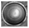
- 2 is a photograph of the sputtering target (sputtering surface) of Example 1. It is a photograph of the sputtering target (sputtering surface) of Example 4.
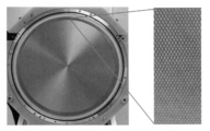
- 6 is a photograph of the sputtering target (sputtering surface) of Example 5. It is a photograph of the sputtering target (sputtering surface) of the comparative example 2.
- the sputtering target of the present invention is characterized in that a processing groove for ignition is arranged in the tapered portion of the sputtering surface. Since the processed grooves arranged in this way easily cause an electron avalanche when generating plasma, it can greatly contribute to the generation and stabilization of ignition. Although this mechanism is not necessarily clear, since the angle when primary charged particles (Ar ions, electrons) enter the processing groove of the target becomes shallow, it is possible to improve the probability of secondary electron emission. Conceivable.
- the repulsive force between the charged particles of the same kind is reduced at the edge portion of the processed groove, it is considered that the electric field concentration occurs and the secondary electron emission probability can be improved. Since the secondary electrons are generated so as to spread in all directions starting from the entry point of the primary charged particles, the emission probability of the secondary electrons is improved in the slope portion than in the flat portion. Furthermore, due to the unevenness of the processed surface, the number of scattering of gas molecules and charged particles increases, and as a result, the number of collisions of charged particles can be improved and the ionization rate can be improved.
- the ignition failure rate of the ignition can be remarkably reduced by forming the processing groove in the tapered portion of the sputter surface as shown in the examples described later.
- the sputtering surface means a surface exposed to the plasma of the sputtering target.
- the taper portion means a chamfered portion at the outer peripheral end portion of the sputtering surface of the sputtering target, and is a portion that does not substantially contribute to film formation or contributes little.
- the flat portion is a portion that substantially contributes to film formation, excluding the tapered portion, on the sputtering surface.
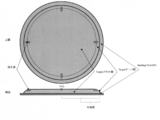
- FIG. 1 (upper view) shows a sputtering surface of the sputtering target
- FIG. 1 (lower view) shows a cross section of the sputtering target. Note that FIG. 1 is merely one form for easy understanding, and the present invention is not limited by this form. The present invention includes various modifications other than those described below.
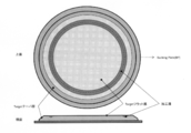
- the processing groove is usually formed in the tapered portion on the sputtering surface side of the target, but it may be formed not only in the tapered portion but also across the flat portion (surface parallel to the opposing wafer surface) as shown in FIG. Good.
- the erosion of the target surface is shallower than 2/3 of the deepest portion and is formed in a portion (low erosion region) with little involvement in film formation. This is because the amount of magnetic flux leakage due to the processed groove changes in the portion where the erosion progresses rapidly, and the influence on the current-voltage change during film formation becomes large.
- a processing groove in a flat portion or a tapered portion in an outer peripheral portion of the target (a region from the half of the length from the center of the target to the outermost end including the tapered portion of the target).
- the processing groove is formed only in the tapered portion or in both the tapered portion and the flat portion may depend on the specifications of the sputtering apparatus, and may be appropriately selected according to the specifications. it can.
- such a processed groove can be formed by machining such as cutting the surface of the sputtering target or knurling (a method of forming an uneven groove on the material surface using a pressing piece or a cutting piece).
- the processing grooves can be arranged at one place or two places, but it is preferable to place a plurality of machining grooves on the target so as to be vertically and horizontally symmetrical like 4 places, 8 places, 16 places, 32 places and the like.
- the magnetron sputtering apparatus acts at least every 1/4 second with respect to the rotation speed of the magnet of about 1 turn / second, and the stability of the ignition can be improved.
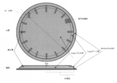
- the processing grooves are formed in a radial shape (radial line starting from the center of the target) as shown in FIG. 3 than in a concentric shape as shown in FIG. There is little decrease (life dependency).
- the angle formed by the parallel or diametrical direction with respect to the diametric direction of the target is within 45 degrees.
- the processing grooves are formed at regular intervals, but if the profile stability of the sputtering film thickness distribution and suppression of dust generation are taken into consideration, they are formed at regular intervals. Preferably it is.
- the cross-sectional shape of the scissors groove can be V-shaped, U-shaped, rectangular, or the like, and the shape can be selected or combined depending on the ease of processing and the occurrence of foreign matter.
- the depth of the processed groove is not particularly limited because it does not relate to the area ratio, but is preferably 0.3 mm or more for the convenience of processing.
- channel provided in two different directions as shown in FIG. 3 may cross
- the above-described processing groove position, angle with the diameter direction, shape, number of locations, and the like are selected in accordance with the specifications of the sputtering apparatus.
- the area ratio of the processing groove When forming a processing groove in the taper part of a heel target, it is preferable that the area ratio of the processing groove shall be 0.6% or more.
- the area ratio of the processed groove means an area projected on the sputter surface of the groove cut out by the processing. When the area ratio of the processed groove in the tapered portion is less than 0.6%, the effect of stabilizing the ignition may be lowered. On the other hand, when the groove is formed across the flat portion of the target, the area ratio of the processed groove is 10% at the maximum with respect to the flat portion.
- the area ratio of the processed groove in the flat portion exceeds 10%, the current value during sputtering decreases, and the applied power may become unstable. Since the taper portion does not affect the applied voltage during sputtering, the taper portion is not included in the calculation of the area ratio. Further, if the processed groove is formed in the above-described tapered portion, it is effective for improving the ignition, and therefore the processed groove does not necessarily have to be formed in the flat portion. In this case, the area ratio of the processed groove in the flat portion is 0%.
- the sputtering surface (flat portion) has a width of 6 mm, length: flat portion 13 mm, taper portion 12 mm, depth 3 mm.
- the area ratio of the processed grooves to the sputtering surface of the target is (6 ⁇ 13 ⁇ 4) / ( ⁇ ⁇ 203 2 ) ⁇ 100 ⁇ 0.24 (%) It becomes. Note that, under the projected area, the area may be the same and the shape may be different, but the difference in shape does not affect so much from the viewpoint of the effect of improving the probability of secondary electron emission due to electrolytic concentration and the edge effect.
- the above-described processed groove is only related to the shape of the sputtering target, and has an effect of improving the ignition regardless of the material and composition of the target. However, it is more effective when used for a sputtering target made of a high-purity material in which the ignition is likely to be unstable, for example, a tantalum target having a purity of 4N5 (99.995%) or more for forming a barrier film for copper wiring. The function can be exhibited.
- the purity of 4N5 (99.995%) means that the dissolved Ta ingot is analyzed by glow discharge mass spectrometry (GDMS), and Na, Al, Si, K, Ti, Cr, Mn, It means that the total value of Fe, Co, Ni, Cu, Zn and Zr is less than 50 ppm.
- GDMS glow discharge mass spectrometry
- Example 1 In a tantalum sputtering target (purity of 4N5 or more) having a diameter of 444 mm and a sputter surface diameter of 406 mm, four V-shaped cross-sectionally processed grooves are provided on the outer periphery of the tantalum sputtering target so as to be equidistant in parallel with the target diameter direction. Formed. A photograph of this target is shown in FIG. The groove width is 6 mm, the groove depth is 3 mm, the groove length is a flat part 13 mm, the taper part 12 mm, the processing groove area ratio of the flat part is 0.24%, and the processing groove area ratio of the taper part is Was 1.1%.
- this target was sputtered under the following conditions, and the ignition failure rate of ignition ((number of ignition failures / number of times of ignition) ⁇ 100) was examined. As a result, the ignition failure rate was significantly reduced from 75% to 34.7% as compared with the same type target having no machining groove.
- the process returns to the beginning of the “ignition” in the second step, and the set power is applied again.
- the application of the set power is repeated three times. If the ignition is not successful even after a total of four times, it is determined that the ignition has failed, and the process is stopped.
- Example 2 In a tantalum sputtering target (purity of 4N5 or more) having a diameter of 444 mm and a sputter surface diameter of 406 mm, four V-shaped cross-sectionally processed grooves were formed on the outer periphery of the tantalum sputtering target at equal intervals in parallel with the target diameter direction. . Groove width 3mm, groove depth 3mm, groove length flat part 13mm, taper part 12mm, flat groove processed groove area ratio 0.12%, tapered groove processed groove area ratio was 0.6%. Next, this target was sputtered under the same conditions as in Example 1, and the ignition failure rate of the ignition was examined. As a result, the ignition failure rate was significantly reduced from 75% to 31.6% as compared with the same type target having no machining groove.
- Example 3 In a tantalum sputtering target (purity 4N5 or more) with a diameter of 444 mm and a sputter surface diameter of 406 mm, four U-shaped processing grooves are formed only at the outer peripheral taper portion so as to be equidistant in parallel to the diameter direction of the target. Formed.
- the groove width is 3 mm
- the groove depth is 3 mm
- the groove length is a flat part 0 mm
- the flat groove processed groove area ratio is 0%
- the taper processed groove area ratio is 0. .6%.
- the ignition failure rate of ignition ((number of ignition failures / number of times of ignition) ⁇ 100) was examined. As a result, the ignition failure rate was significantly reduced from 75% to 33.7% as compared with the same type target having no machining groove.
- Example 4 In a tantalum sputtering target (purity 4N5 or more) having a diameter of 444 mm and a sputter surface diameter of 406 mm, 32 U-shaped processing grooves are formed only at the outer peripheral taper portion so as to be equidistant in parallel with the target diameter direction. Formed. A photograph of this target is shown in FIG. The width of the groove is 3 mm, the depth of the groove is 3 mm, the length of the groove is a flat part 0 mm, and the taper part 12 mm. The area ratio of the processing groove in the flat part is 0%, and the area ratio of the processing groove in the taper part is 4. 0.5%.
- this target was sputtered under the following conditions, and the ignition failure rate of ignition ((number of ignition failures / number of times of ignition) ⁇ 100) was examined. As a result, the ignition failure rate was significantly reduced from 75% to 7.4% compared to the same type target without the machining groove.
- Example 5 In a tantalum sputtering target having a diameter of 444 mm and a sputter surface diameter of 406 mm (purity of 4N5 or more), a V-shaped cross-sectionally processed groove is formed at an angle of ⁇ 45 degrees with respect to the diameter direction of the target at all of the outer peripheral tapered portion. Thus, a knurling process was performed at equal intervals of 1 mm to form a lattice pattern. A photograph of the processed groove portion of this target is shown in FIG. The groove width was 1 mm, the groove depth was 0.1 mm, the flat groove processed groove area ratio was 0%, and the tapered groove processed groove area ratio was 90%.
- this target was sputtered under the following conditions, and the ignition failure rate of ignition ((number of ignition failures / number of times of ignition) ⁇ 100) was examined. As a result, the ignition failure rate was significantly reduced from 75% to 3.2% as compared with the same type target having no machining groove.
- Example 6 In a tantalum sputtering target (purity 4N5 or more) having a diameter of 444 mm and a sputter surface diameter of 406 mm, four U-shaped processing grooves are formed in the outer peripheral taper portion so as to be equidistant in parallel with the target diameter direction.
- the groove width was 3 mm
- the groove depth was 3 mm
- the groove length was 0 mm flat
- the taper was 12 mm.
- a processing groove having a V-shaped cross section was formed concentrically on the outer peripheral portion, the groove width was 6 mm, the depth was 3 mm, the groove length was about 1256 mm for the outer periphery, and about 1193 mm for the inner periphery.
- the area ratio of the processing groove in the taper portion was 0.6% and the area ratio of the processing groove in the flat portion was 9.5% due to the two types of processing grooves.
- this target was sputtered under the following conditions, and the ignition failure rate of ignition ((number of ignition failures / number of times of ignition) ⁇ 100) was examined. As a result, the ignition failure rate was significantly reduced from 75% to 25.3% as compared with the same type target having no machining groove.
- Example 1 A tantalum sputtering target (purity 4N5 or more) having a diameter of 444 mm and a sputter surface diameter of 406 mm was prepared without a processing groove. This target was sputtered under the same conditions as in Example 1, and the ignition failure rate of ignition ((number of ignition failures / number of times of ignition) ⁇ 100) was examined. As a result, the ignition failure rate was 75.0%.
- this target was sputtered under the same conditions as in Example 1, and the ignition failure rate of ignition ((number of ignition failures / number of times of ignition) ⁇ 100) was examined. As a result, the ignition failure rate was not significantly reduced from 75.0% to 70.9% compared to the same type target having no machining groove.
- the sputtering target of the present invention can reduce the ignition failure rate of ignition (plasma ignition) even under conditions such as reduction of introduced gas and shortened voltage application time, and can stably start a sputtering process. Make it possible. Thereby, the downtime of the apparatus can be shortened, which can contribute to an improvement in throughput and cost performance.
- the sputtering target of the present invention is useful for forming a thin film for electronic devices.
Landscapes
- Chemical & Material Sciences (AREA)
- Engineering & Computer Science (AREA)
- Physics & Mathematics (AREA)
- Plasma & Fusion (AREA)
- Analytical Chemistry (AREA)
- Chemical Kinetics & Catalysis (AREA)
- Materials Engineering (AREA)
- Mechanical Engineering (AREA)
- Metallurgy (AREA)
- Organic Chemistry (AREA)
- Physical Vapour Deposition (AREA)
- Electrodes Of Semiconductors (AREA)
Abstract
Description
1)フラット部とテーパ部を備えたスパッタリングターゲットにおいて、スパッタリングターゲットのテーパ部に加工溝が配置されていることを特徴とするスパッタリングターゲット。
2)前記テーパ部の加工溝の面積比率が0.6%以上であることを特徴とする上記1)記載のスパッタリングターゲット。
3)前記フラット部の加工溝の面積比率が10%以下であることを特徴とする上記1)又は2)記載のスパッタリングターゲット。
4)前記加工溝の深さが0.1mm以上であることを特徴とする上記1)~3)のいずれか一に記載のスパッタリングターゲット。
5)純度4N5以上のタンタルからなることを特徴とする上記1)~4)のいずれか一項に記載のスパッタリングターゲット。
直径444mm、スパッタ面の直径が406mmのタンタルスパッタリングターゲット(純度4N5以上)において、その外周部に断面V字型の加工溝をターゲットの直径方向に対して平行に、等間隔となるように4ヶ所形成した。このターゲットの写真を図4に示す。溝の幅を6mm、溝の深さを3mm、溝の長さをフラット部13mm、テーパ部12mmとし、フラット部の加工溝の面積比率を0.24%とし、テーパ部の加工溝の面積比率を1.1%とした。次に、このターゲットを以下の条件でスパッタリングを実施し、イグニッションの点火失敗率((イグニッション失敗回数/イグニッション実施回数)×100)を調べた。その結果、加工溝がない同型のターゲットに比べて、点火失敗率は、75%から34.7%まで著しく低下した。
第1ステップ「ガス安定」(5sec)
Arガスを5sccm導入する。
第2ステップ「イグニッション」(1sec(点火まで5sec))
Arガスを5sccm導入したまま、DC電源で1000W印加する。
(真空度:0.2~0.3mTorr)
第3ステップ「真空引き」(10sec)
チャンバ内の真空引きを行う(真空度:1~3μTorr)。
上記3ステップを1サイクルとして、点火試験を実施する。イグニッションの成否は、第2ステップの「イグニッション」において、印可開始から5sec以内に実電力に到達したかで判断する。5sec以内にイグニッションが成功しなかった場合、第2ステップの「イグニッション」の始めに戻り、設定電力を再度印加する。この第2ステップの「イグニッション」で設定電力の印加を3回繰り返し、合計4回行ってもイグニッションが成功しない場合は点火失敗と判断し、処理を停止する。
直径444mm、スパッタ面の直径が406mmのタンタルスパッタリングターゲット(純度4N5以上)において、その外周部に断面V字型の加工溝をターゲットの直径方向と平行に、等間隔となるように4ヶ所形成した。溝の幅を3mm、溝の深さを3mm、溝の長さをフラット部13mm、テーパ部12mmとし、フラット部の加工溝の面積比率を0.12%とし、テーパ部の加工溝の面積比率を0.6%とした。次に、このターゲットを実施例1と同条件にて、スパッタを実施して、イグニッションの点火失敗率を調べた。その結果、加工溝がない同型のターゲットに比べて、点火失敗率は、75%から31.6%まで著しく低下した。
直径444mm、スパッタ面の直径が406mmのタンタルスパッタリングターゲット(純度4N5以上)において、その外周テーパ部のみに断面U字型の加工溝をターゲットの直径方向と平行に、等間隔となるように4ヶ所形成した。溝の幅を3mm、溝の深さを3mm、溝の長さをフラット部0mm、テーパ部12mmとし、フラット部の加工溝の面積比率を0%とし、テーパ部の加工溝の面積比率を0.6%とした。次に、このターゲットをバッキングプレートに接合した後、以下の条件でスパッタリングを実施し、イグニッションの点火失敗率((イグニッション失敗回数/イグニッション実施回数)×100)を調べた。その結果、加工溝がない同型のターゲットに比べて、点火失敗率は、75%から33.7%まで著しく低下した。
直径444mm、スパッタ面の直径が406mmのタンタルスパッタリングターゲット(純度4N5以上)において、その外周テーパ部のみに断面U字型の加工溝をターゲットの直径方向と平行に、等間隔となるように32ヶ所形成した。このターゲットの写真を図5に示す。溝の幅を3mm、溝の深さを3mm、溝の長さをフラット部0mm、テーパ部12mmとし、フラット部の加工溝の面積比率を0%とし、テーパ部の加工溝の面積比率を4.5%とした。次に、このターゲットを以下の条件でスパッタリングを実施し、イグニッションの点火失敗率((イグニッション失敗回数/イグニッション実施回数)×100)を調べた。その結果、加工溝がない同型のターゲットに比べて、点火失敗率は、75%から7.4%まで著しく低下した。
直径444mm、スパッタ面の直径が406mmのタンタルスパッタリングターゲット(純度4N5以上)において、その外周テーパ部の全てに、断面V字型の加工溝をターゲットの直径方向に対して±45度の角度を成すように1mmの等間隔でナーリング加工して、格子状模様を形成した。このターゲットの加工溝部分の写真を図6に示す。溝の幅を1mm、溝の深さを0.1mm、フラット部の加工溝の面積比率を0%とし、テーパ部の加工溝の面積比率を90%とした。次に、このターゲットを以下の条件でスパッタリングを実施し、イグニッションの点火失敗率((イグニッション失敗回数/イグニッション実施回数)×100)を調べた。その結果、加工溝がない同型のターゲットに比べて、点火失敗率は、75%から3.2%まで著しく低下した。
直径444mm、スパッタ面の直径が406mmのタンタルスパッタリングターゲット(純度4N5以上)において、その外周テーパ部に断面U字型の加工溝をターゲットの直径方向と平行に、等間隔となるように4ヶ所形成し、溝の幅を3mm、溝の深さを3mm、溝の長さをフラット部0mm、テーパ部12mmとした。合わせて、外周部に断面V字型の加工溝を同心円状に形成し、溝の幅を6mm、深さを3mm、溝の長さを外周約1256mm、内周約1193mmとした。上記2種類の加工溝によりテーパ部の加工溝の面積比率を0.6%とし、フラット部の加工溝の面積比率を9.5%とした。次に、このターゲットを以下の条件でスパッタリングを実施し、イグニッションの点火失敗率((イグニッション失敗回数/イグニッション実施回数)×100)を調べた。その結果、加工溝がない同型のターゲットに比べて、点火失敗率は、75%から25.3%まで著しく低下した。
直径444mm、スパッタ面の直径が406mmのタンタルスパッタリングターゲット(純度4N5以上)において、加工溝が無いターゲットを作製した。このターゲットを実施例1と同条件にて、スパッタを実施して、イグニッションの点火失敗率((イグニッション失敗回数/イグニッション実施回数)×100)を調べた。その結果、点火失敗率は75.0%であった。
直径444mmのタンタルスパッタリングターゲット(純度3N5以上)において、その外周部に断面V字型の加工溝を同心円状に形成した。このターゲットの写真を図7に示す。溝の幅を6mm、深さを3mm、溝の長さを外周約1256mm、内周約1193mmとし、フラット部の加工溝の面積比率を9.5%とし、テーパ部の加工溝の面積比率を0%とした。次に、このターゲットを実施例1と同条件にて、スパッタを実施して、イグニッションの点火失敗率((イグニッション失敗回数/イグニッション実施回数)×100)を調べた。その結果、加工溝がない同型のターゲットに比べて、点火失敗率は、75.0%から70.9%と大きな低下は見られなかった。
直径444mmのタンタルスパッタリングターゲット(純度3N5以上)において、その外周部に断面V字型の加工溝を同心円状に形成した。溝の幅は14mm、深さは3mm、溝の長さは外周約1237mm、内周約1150mmとし、フラット部の加工溝の面積比率は11.1%とし、テーパ部の加工溝の面積比率を0%とした。次に、このターゲットを実施例1と同条件にて、スパッタを実施したところ、スパッタ時の電流値が低下し、スパッタ電力が安定しない現象が見られたため、評価を中止した。
直径444mm、スパッタ面の直径が406mmのタンタルスパッタリングターゲット(純度4N5以上)において、その外周フラット部のみに断面U字型の加工溝をターゲットの直径方向と平行に、等間隔となるように4ヶ所形成した。溝の幅を3mm、溝の深さを3mm、溝の長さをフラット部13mm、テーパ部0mmとし、フラット部の加工溝の面積比率を0.24%とし、テーパ部の加工溝の面積比率を0%とした。次に、このターゲットをバッキングプレートに接合した後、以下の条件でスパッタリングを実施し、イグニッションの点火失敗率((イグニッション失敗回数/イグニッション実施回数)×100)を調べた。その結果、加工溝がない同型のターゲットに比べて、点火失敗率は、75%から68.5%と大きな低下はみられなかった。

Claims (5)
- フラット部とテーパ部を備えたスパッタリングターゲットにおいて、スパッタリングターゲットのテーパ部に加工溝が配置されていることを特徴とするスパッタリングターゲット。
- 前記テーパ部の加工溝の面積比率が0.6%以上であることを特徴とする請求項1記載のスパッタリングターゲット。
- 前記フラット部の加工溝の面積比率が10%以下であることを特徴とする請求項1~2のいずれか一項に記載のスパッタリングターゲット。
- 前記加工溝の深さが0.1mm以上であることを特徴とする請求項1~3のいずれか一項に記載のスパッタリングターゲット。
- 純度4N5以上のタンタルからなることを特徴とする請求項1~4のいずれか一項に記載のスパッタリングターゲット。
Priority Applications (5)
| Application Number | Priority Date | Filing Date | Title |
|---|---|---|---|
| US15/575,063 US10984992B2 (en) | 2015-05-21 | 2016-05-18 | Sputtering target |
| KR1020177034242A KR20170141761A (ko) | 2015-05-21 | 2016-05-18 | 스퍼터링 타깃 |
| JP2017519374A JP6367483B2 (ja) | 2015-05-21 | 2016-05-18 | スパッタリングターゲット |
| CN201680028414.2A CN107614742B (zh) | 2015-05-21 | 2016-05-18 | 溅射靶 |
| KR1020207032299A KR102389342B1 (ko) | 2015-05-21 | 2016-05-18 | 스퍼터링 타깃 |
Applications Claiming Priority (4)
| Application Number | Priority Date | Filing Date | Title |
|---|---|---|---|
| JP2015103981 | 2015-05-21 | ||
| JP2015-103981 | 2015-05-21 | ||
| JP2015113150 | 2015-06-03 | ||
| JP2015-113150 | 2015-06-03 |
Publications (1)
| Publication Number | Publication Date |
|---|---|
| WO2016186119A1 true WO2016186119A1 (ja) | 2016-11-24 |
Family
ID=57320109
Family Applications (1)
| Application Number | Title | Priority Date | Filing Date |
|---|---|---|---|
| PCT/JP2016/064667 Ceased WO2016186119A1 (ja) | 2015-05-21 | 2016-05-18 | スパッタリングターゲット |
Country Status (6)
| Country | Link |
|---|---|
| US (1) | US10984992B2 (ja) |
| JP (2) | JP6367483B2 (ja) |
| KR (2) | KR20170141761A (ja) |
| CN (1) | CN107614742B (ja) |
| TW (1) | TWI695076B (ja) |
| WO (1) | WO2016186119A1 (ja) |
Families Citing this family (4)
| Publication number | Priority date | Publication date | Assignee | Title |
|---|---|---|---|---|
| CN111725091A (zh) * | 2019-03-22 | 2020-09-29 | 北京北方华创微电子装备有限公司 | 优化工艺流程的方法及装置、存储介质和半导体处理设备 |
| JP6586540B1 (ja) * | 2019-03-28 | 2019-10-02 | Jx金属株式会社 | ターゲット材とバッキングプレートとの接合体、および、ターゲット材とバッキングプレートとの接合体の製造方法 |
| DE102021104255A1 (de) * | 2021-02-23 | 2022-08-25 | Cemecon Ag. | Zerstäubungstarget |
| US12559833B2 (en) * | 2023-10-19 | 2026-02-24 | Taiwan Semiconductor Manufacturing Company Ltd. | PVD target structure and method for preparing the same |
Citations (3)
| Publication number | Priority date | Publication date | Assignee | Title |
|---|---|---|---|---|
| JP2005538257A (ja) * | 2002-07-16 | 2005-12-15 | ハネウェル・インターナショナル・インコーポレーテッド | Pvdターゲット構造の非スパッタ領域を処理して粒子トラップを形成する方法、及び非スパッタ領域に沿った突出部を含むpvdターゲット構造 |
| JP2012104605A (ja) * | 2010-11-09 | 2012-05-31 | Shinkawa Ltd | プラズマ装置およびその製造方法 |
| WO2015050041A1 (ja) * | 2013-10-01 | 2015-04-09 | Jx日鉱日石金属株式会社 | タンタルスパッタリングターゲット |
Family Cites Families (11)
| Publication number | Priority date | Publication date | Assignee | Title |
|---|---|---|---|---|
| EP0625792B1 (en) * | 1993-05-19 | 1997-05-28 | Applied Materials, Inc. | Apparatus and process for increasing uniformity of sputtering rate in sputtering apparatus |
| US6117281A (en) * | 1998-01-08 | 2000-09-12 | Seagate Technology, Inc. | Magnetron sputtering target for reduced contamination |
| JP3791829B2 (ja) | 2000-08-25 | 2006-06-28 | 株式会社日鉱マテリアルズ | パーティクル発生の少ないスパッタリングターゲット |
| US6503380B1 (en) * | 2000-10-13 | 2003-01-07 | Honeywell International Inc. | Physical vapor target constructions |
| JP2003027225A (ja) | 2001-07-13 | 2003-01-29 | Canon Inc | スパッタリングターゲットおよびスパッタリング装置 |
| JP4007010B2 (ja) | 2002-02-04 | 2007-11-14 | ヤマハ株式会社 | スパッタリングターゲット |
| JP2004084007A (ja) | 2002-08-27 | 2004-03-18 | Nec Kyushu Ltd | スパッタ装置 |
| US20050072668A1 (en) | 2003-10-06 | 2005-04-07 | Heraeus, Inc. | Sputter target having modified surface texture |
| EP2236644A3 (en) * | 2004-11-17 | 2012-01-04 | JX Nippon Mining & Metals Corporation | Sputtering target backing plate assembly and film deposition system |
| CN101720493B (zh) * | 2007-06-15 | 2012-08-15 | Oc欧瑞康巴尔斯公司 | 多靶溅射源及沉积多层的方法 |
| KR20150126376A (ko) | 2013-09-12 | 2015-11-11 | 제이엑스 닛코 닛세키 킨조쿠 가부시키가이샤 | 배킹 플레이트 일체형의 금속제 스퍼터링 타깃 및 그 제조 방법 |
-
2016
- 2016-05-18 US US15/575,063 patent/US10984992B2/en active Active
- 2016-05-18 WO PCT/JP2016/064667 patent/WO2016186119A1/ja not_active Ceased
- 2016-05-18 KR KR1020177034242A patent/KR20170141761A/ko not_active Ceased
- 2016-05-18 CN CN201680028414.2A patent/CN107614742B/zh active Active
- 2016-05-18 KR KR1020207032299A patent/KR102389342B1/ko active Active
- 2016-05-18 JP JP2017519374A patent/JP6367483B2/ja active Active
- 2016-05-19 TW TW105115509A patent/TWI695076B/zh active
-
2018
- 2018-05-30 JP JP2018103619A patent/JP6847076B2/ja active Active
Patent Citations (3)
| Publication number | Priority date | Publication date | Assignee | Title |
|---|---|---|---|---|
| JP2005538257A (ja) * | 2002-07-16 | 2005-12-15 | ハネウェル・インターナショナル・インコーポレーテッド | Pvdターゲット構造の非スパッタ領域を処理して粒子トラップを形成する方法、及び非スパッタ領域に沿った突出部を含むpvdターゲット構造 |
| JP2012104605A (ja) * | 2010-11-09 | 2012-05-31 | Shinkawa Ltd | プラズマ装置およびその製造方法 |
| WO2015050041A1 (ja) * | 2013-10-01 | 2015-04-09 | Jx日鉱日石金属株式会社 | タンタルスパッタリングターゲット |
Also Published As
| Publication number | Publication date |
|---|---|
| US20180144912A1 (en) | 2018-05-24 |
| CN107614742B (zh) | 2020-08-07 |
| KR102389342B1 (ko) | 2022-04-22 |
| KR20170141761A (ko) | 2017-12-26 |
| JPWO2016186119A1 (ja) | 2017-10-19 |
| JP2018159132A (ja) | 2018-10-11 |
| US10984992B2 (en) | 2021-04-20 |
| TW201710532A (zh) | 2017-03-16 |
| KR20200129190A (ko) | 2020-11-17 |
| TWI695076B (zh) | 2020-06-01 |
| JP6367483B2 (ja) | 2018-08-01 |
| CN107614742A (zh) | 2018-01-19 |
| JP6847076B2 (ja) | 2021-03-24 |
Similar Documents
| Publication | Publication Date | Title |
|---|---|---|
| US9685307B2 (en) | Sputtering target, sputtering target-backing plate assembly and deposition system | |
| US20110011737A1 (en) | High-power pulse magnetron sputtering apparatus and surface treatment apparatus using the same | |
| JP6847076B2 (ja) | スパッタリングターゲット | |
| US6099705A (en) | Physical vapor deposition device for forming a uniform metal layer on a semiconductor wafer | |
| JP6496879B2 (ja) | イグニッションを安定化することが可能なスパッタリングターゲット | |
| JP4902051B2 (ja) | バイアススパッタリング装置 | |
| JP6498527B2 (ja) | スパッタリングターゲット | |
| JP5650411B2 (ja) | プラズマ蒸着方法 | |
| JP2016191109A (ja) | タンタルスパッタリングターゲット | |
| US8337675B2 (en) | Method of plasma vapour deposition | |
| US8907301B1 (en) | Gas mixture method for generating ion beam | |
| TWI639719B (zh) | 直流磁控電弧鍍膜裝置及其方法 | |
| JP5995811B2 (ja) | 銅膜の成膜方法 | |
| JP2012009179A (ja) | 硼化ランタン膜の製造方法 |
Legal Events
| Date | Code | Title | Description |
|---|---|---|---|
| 121 | Ep: the epo has been informed by wipo that ep was designated in this application |
Ref document number: 16796512 Country of ref document: EP Kind code of ref document: A1 |
|
| ENP | Entry into the national phase |
Ref document number: 2017519374 Country of ref document: JP Kind code of ref document: A |
|
| WWE | Wipo information: entry into national phase |
Ref document number: 15575063 Country of ref document: US |
|
| NENP | Non-entry into the national phase |
Ref country code: DE |
|
| ENP | Entry into the national phase |
Ref document number: 20177034242 Country of ref document: KR Kind code of ref document: A |
|
| 122 | Ep: pct application non-entry in european phase |
Ref document number: 16796512 Country of ref document: EP Kind code of ref document: A1 |