WO2016181553A1 - 表面実装型の遮蔽ユニット及び遮蔽ユニットを備える電子機器 - Google Patents
表面実装型の遮蔽ユニット及び遮蔽ユニットを備える電子機器 Download PDFInfo
- Publication number
- WO2016181553A1 WO2016181553A1 PCT/JP2015/063927 JP2015063927W WO2016181553A1 WO 2016181553 A1 WO2016181553 A1 WO 2016181553A1 JP 2015063927 W JP2015063927 W JP 2015063927W WO 2016181553 A1 WO2016181553 A1 WO 2016181553A1
- Authority
- WO
- WIPO (PCT)
- Prior art keywords
- partition wall
- frame
- cap
- substrate
- shielding unit
- Prior art date
- Legal status (The legal status is an assumption and is not a legal conclusion. Google has not performed a legal analysis and makes no representation as to the accuracy of the status listed.)
- Ceased
Links
Images











Classifications
-
- H—ELECTRICITY
- H05—ELECTRIC TECHNIQUES NOT OTHERWISE PROVIDED FOR
- H05K—PRINTED CIRCUITS; CASINGS OR CONSTRUCTIONAL DETAILS OF ELECTRIC APPARATUS; MANUFACTURE OF ASSEMBLAGES OF ELECTRICAL COMPONENTS
- H05K9/00—Screening of apparatus or components against electric or magnetic fields
Definitions
- This application relates to a surface mount type shielding unit and an electronic device including the shielding unit.
- Electronic devices having a wireless communication function such as mobile phones, tablet terminals, and mobile PCs include various electronic components such as a high-speed CPU and a memory on the same substrate in addition to wireless components.
- the sensitivity of the wireless component may deteriorate due to radiation noise from the CPU and memory or noise interference between the wireless components.
- the influence of unnecessary radiation noise is reduced by mounting a noise shielding frame unit that covers electronic components on a substrate.
- the noise shielding frame unit includes a small sheet metal frame that independently covers one electronic component that is a noise generation source, and a large sheet metal frame that collectively covers a plurality of electronic components. included.
- the latter frame unit has an internal partition for dividing a space surrounded by the sheet metal frame. Therefore, the latter frame unit may be referred to as a “partitioned” frame unit below. Further, the former frame unit may be hereinafter referred to as a “no partition” frame unit for comparison with a “partition” frame unit.
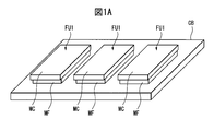
- FIG. 1A is a perspective view showing a circuit board CB on which a frame unit FU1 without partition is mounted.
- 1B is a top view of the circuit board CB and the frame unit FU1 in FIG. 1A
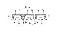
- FIG. 1C is a cross-sectional view taken along line 1C-1C in FIG. 1B.
- three frame units FU1 that independently cover three electronic components EC arranged in the left-right direction are mounted on a circuit board CB.
- the undivided frame unit FU1 has a sheet metal frame MF and a sheet metal cap MC formed in accordance with the dimensions and mounting conditions of the individual electronic components EC.
- FIG. 2A is a perspective view showing the circuit board CB on which the frame unit with partition FU2 is mounted.
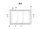
- 2B is a top view of the circuit board CB and the frame unit FU2 in FIG. 2A
- FIG. 2C is a cross-sectional view taken along line 2C-2C in FIG. 2B.
- a single frame unit FU2 that collectively covers three electronic components EC arranged in the left-right direction is mounted on the circuit board CB.
- the frame unit FU2 with partitions has two internal partitions IP that divide the space surrounded by the sheet metal frame, and each internal partition IP includes the adjacent electronic components EC, It is arranged between ECs.
- the partition-attached frame unit FU2 When the partition-attached frame unit FU2 is used, the clearance between the sheet metal frames is not provided, so that the mounting area on the circuit board CB becomes relatively small.
- a contact failure between the sheet metal cap MP and the internal partition IP may occur due to manufacturing errors such as the internal partition IP and the sheet metal cap MC.
- the sheet metal cap MC may be partially lifted by the internal partition IP due to manufacturing errors such as the internal partition IP and the sheet metal cap MC. The above event will be described with reference to FIGS. 3A to 3D.
- FIG. 3A is a cross-sectional view showing a circuit board CB on which a frame unit F3 with a partition similar to the frame unit FU2 in FIGS. 2A to 2C is mounted.
- FIG. 3A also shows a device case CS attached above the circuit board CB (the same applies to FIGS. 3B to 3D described later).
- the electromagnetic wave noise NZ radiated from one electronic component EC passes through the internal partition IP to the other electronic component EC.
- the sheet metal cap MC is not lifted by the internal partition IP.
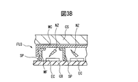
- FIG. 3B is a cross-sectional view similar to FIG. 3A and shows the frame unit FU3 in which the internal partition IP is lower than the sheet metal frame due to manufacturing errors.
- the electromagnetic wave noise NZ radiated from one electronic component EC passes through the internal partition IP to the other electronic component EC. There is a risk of reaching. As a result, noise interference may occur between the adjacent electronic components EC and EC.
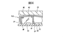
- FIG. 3C is a cross-sectional view similar to FIG. 3A, showing the frame unit FU3 in which the internal partition IP is higher than the sheet metal frame MF due to manufacturing errors. In the example of FIG.
- the height of the gap between the circuit board CB and the device case CS is designed to include a clearance for preventing the sheet metal cap MC from contacting the device case CS.
- the clearance is determined in consideration of the dimensional tolerance of the internal partition IP.
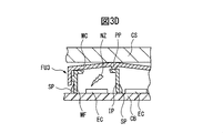
- FIG. 3D is a cross-sectional view similar to FIG. 3A, and shows a frame unit FU3 in which a projection PP is provided on the inner surface of the sheet metal cap MC to ensure contact with the internal partition IP. Also in the example of FIG. 3D, since a part of the sheet metal cap MC is lifted by the internal partition IP, the height of the gap between the circuit board CB and the device case CS is designed to include the clearance. Yes.
- the design in which the height of the gap between the circuit board CB and the device case CS is increased as shown in FIGS. 3C and 3D is disadvantageous in downsizing the device (particularly in reducing the thickness).
- the present invention has been made in view of the above-described problems, and an object of the present invention is a surface mount type that eliminates the lifting of the cap due to the partition wall while ensuring contact between the cap and the partition wall in the frame. Is to provide a shielding unit.
- a frame that surrounds a plurality of electronic components installed on the upper surface of the substrate, a partition wall that partitions a space inside the frame in which the plurality of electronic components are arranged, and a top plate that covers the frame A side plate facing the outer surface of the frame, and a cap having an inclined surface formed so as to be slidably contactable with the partition wall at a position facing the partition wall on the inner surface of the top plate. It has a support part that supports the side plate so that the outer edge of the plate can move in the direction toward or away from the partition wall, and the cap is interlocked with the inclined surface sliding obliquely downward with respect to the partition wall.
- a surface-mount type shielding unit is provided in which the outer edge portion is formed so as to move in a direction toward the partition wall or in a direction away from the partition wall.
- the disclosed shielding unit even if the cap is lifted by the partition wall due to a dimensional error of the partition wall, the lifted portion of the top plate is moved diagonally downward by pressing the top plate toward the substrate. Can be made. Therefore, according to the disclosed shielding unit, it is possible to eliminate the lifting of the cap due to the partition wall while ensuring the contact between the cap and the partition wall.
- FIG. 1A is a perspective view showing a circuit board on which a frame unit without partition is mounted.
- FIG. 1B is a top view of the circuit board and the frame unit in FIG. 1A.
- 1C is a cross-sectional view taken along line 1C-1C in FIG. 1B.
- FIG. 2A is a perspective view showing a circuit board on which a frame unit without partition is mounted.
- 2B is a top view of the circuit board and the frame unit in FIG. 2A.
- 2C is a cross-sectional view taken along line 2C-2C in FIG. 2B.
- FIG. 3A is a cross-sectional view showing a circuit board on which a frame unit with a partition similar to the frame unit in FIGS. 2A to 2C is mounted.
- FIG. 3A is a cross-sectional view showing a circuit board on which a frame unit with a partition similar to the frame unit in FIGS. 2A to 2C is mounted.
- FIG. 3B is a cross-sectional view similar to FIG. 3A, showing a frame unit in which the internal partition is lower than the sheet metal frame due to manufacturing errors.
- FIG. 3C is a cross-sectional view similar to FIG. 3A, showing a frame unit in which the internal partition is higher than the sheet metal frame due to manufacturing errors.
- FIG. 3D is a cross-sectional view similar to FIG. 3A, showing a frame unit in which a protrusion for ensuring contact with the internal partition is provided on the inner surface of the top plate of the sheet metal cap.
- FIG. 4A is an exploded perspective view of an electronic device ED including a surface mount type shielding unit 1 according to an embodiment of the present application.
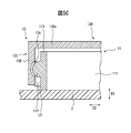
- FIG. 4B is a cross-sectional view perpendicular to the longitudinal direction of the electronic apparatus of FIG. 4A.
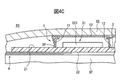
- 4C is an enlarged cross-sectional view of a portion surrounded by a broken line in FIG. 4B.
- FIG. 5A is a perspective view schematically showing the shielding unit and the substrate in FIGS. 4B and 4C.
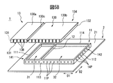
- FIG. 5B is an exploded perspective view corresponding to FIG. 5A and shows a state where the cap of the shielding unit in FIG. 5A is removed from the frame.
- 5C is a cross-sectional view perpendicular to the horizontal direction of the shielding unit and the substrate in FIG. 5A.
- 6A is a cross-sectional view perpendicular to the front-rear direction of the shielding unit and the substrate in FIG.
- FIG. 5A shows a state before the device case is attached to the substrate.
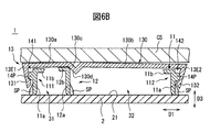
- FIG. 6B is a cross-sectional view perpendicular to the front-rear direction of the shielding unit and the substrate in FIG. 5A and shows a state after the device case CS is attached to the substrate.
- FIG. 7A is an enlarged view showing the vicinity of the first side wall and the partition wall in FIG. 6A.
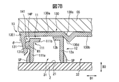
- FIG. 7B is an enlarged view showing the vicinity of the first side wall and the partition wall in FIG. 6B.
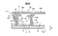
- FIG. 8A is an enlarged view similar to FIG. 7A and shows a shielding unit in which the partition wall is lower than the side wall of the frame due to manufacturing errors.
- FIG. 8B is an enlarged view similar to FIG.
- FIG. 7B shows the shielding unit in which the partition wall is lower than the side wall of the frame due to manufacturing errors.
- FIG. 9A is an enlarged view similar to FIG. 7A and shows a first modification of the cap of the shielding unit.
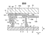
- FIG. 9B is an enlarged view similar to FIG. 7B and shows a first modification of the cap of the shielding unit.
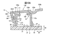
- FIG. 10A is an enlarged view similar to FIG. 7A and shows a second modification of the cap of the shielding unit.
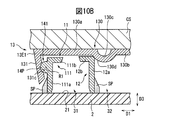
- FIG. 10B is an enlarged view similar to FIG. 7B and shows a second modification of the cap of the shielding unit.
- a wireless communication device such as a mobile phone or a smartphone is illustrated as an electronic device including a surface-mount type shielding unit.
- the electronic device including the surface mount type shielding unit may be another device having a wireless communication function such as a tablet terminal or a mobile PC.
- FIG. 4A is an exploded perspective view of an electronic device ED including a surface mount type shielding unit 1 according to an embodiment of the present application.
- the electronic device ED is a thin wireless communication device such as a mobile phone or a smartphone, and the shielding unit 1 is mounted on a substrate 2 disposed inside the device case CS of the electronic device ED.
- the electronic device ED includes a flat display unit DU, a device case CS attached to the back side of the display unit DU, and a substrate 2 disposed between the display unit DU and the device case CS. is doing.
- the electronic device ED includes a flat battery BT disposed between the display unit DU and the substrate 2.
- FIG. 4B is a cross-sectional view perpendicular to the longitudinal direction of the electronic device ED of FIG. 4A.
- the display unit DU includes a display panel DP such as an LCD panel that forms a display screen of the electronic device ED, and a display control unit DC such as an LCD controller located on the back surface of the display panel DP.
- the battery BT is a secondary battery such as a lithium ion battery or a nickel metal hydride battery.
- the device case CS has a convex curved cross section protruding in a direction away from the back surface of the display panel DP, and the edge of the device case CS in the horizontal direction is displayed on the display panel by a mounting member M having a predetermined shape. It is fixedly attached to the DP.
- An internal space for accommodating the display control unit DC, the battery BT, the substrate 2 and the shielding unit 1 is formed between the inner surface of the device case CS and the back surface of the display panel DP.
- the substrate 2 is a flat plate member for fixing and wiring various electronic components.
- the board 2 is, for example, a printed board.
- the electronic device ED includes a plurality of electronic components EC1 and EC2 mounted on the upper surface 21 of the substrate 2 facing the inner surface of the device case CS.
- the shielding unit 1 is mounted on the upper surface 21 of the substrate 2 by the soldering part SP so as to cover the plurality of electronic components EC1 and EC2 together. That is, the shielding unit 1 plays a role of shielding electromagnetic noise radiated from the plurality of electronic components EC1 and EC2 on the substrate 2.
- 4C is an enlarged cross-sectional view of a portion surrounded by a broken line in FIG. 4B. As shown in FIG.
- the electronic device ED includes a substrate holding member H attached to the lower surface 22 of the substrate 2 so as to support the substrate 2, and the substrate holding member H is formed by laminating two thin plates. Is formed by.
- the substrate holding member H is fixed to the mounting member M via a fixing member F having a predetermined shape (see FIG. 4B). That is, the device case CS is attached to the substrate 2 via the attachment member M, the fixing member F, and the substrate holding member H.
- the shielding unit 1 includes a frame 11 that is mounted on the upper surface 21 of the substrate 2 so as to surround the plurality of electronic components EC1 and EC2, and a frame that partitions the space inside the frame 11. 11 and the partition wall 12 attached to 11. Furthermore, the shielding unit 1 has a cap 13 attached to the frame 11 so as to cover the upper part of the frame 11.
- the frame 11, the partition wall 12, and the cap 13 of the shielding unit 1 are made of various conductive materials that block electromagnetic waves, and are made of, for example, metal materials such as copper, aluminum, and brass. The structure of each part of the shielding unit 1 will be described with reference to FIGS. 5A to 5C and the like.
- FIG. 5A is a perspective view schematically showing the substrate 2 and the shielding unit 1 in FIGS. 4A to 4C
- FIG. 5B is an exploded perspective view corresponding to FIG. 5A, and shows the shielding unit 1 in FIG. 5A.
- a state where the cap 13 is removed from the frame 11 is shown.
- illustration of a plurality of electronic components EC1 and EC2 mounted on the substrate 2 is omitted.
- the frame 11 of the shielding unit 1 includes a first side wall 111 and a second side wall 112 that extend parallel to each other along the upper surface 21 of the substrate 2, and a first side wall 111 and a second side wall 112.
- the direction in which the two side walls 111 and 112 are arranged is referred to as the left-right direction
- the direction in which the front wall 113 and the rear wall 114 are arranged is referred to as the front-rear direction.
- the left-right direction is represented by an arrow D1
- the front-rear direction is represented by an arrow D2 (the same applies to other drawings).
- the partition wall 12 of the shielding unit 1 is located between the first and second side walls 111 and 112 and extends in parallel with the first and second side walls 111 and 112.
- the internal space of the frame 11 located between the first side wall 111 and the partition wall 12 is referred to as a first internal space 31, and the frame located between the second side wall 112 and the partition wall 12 is referred to as the first internal space 31.
- the internal space is referred to as a second internal space 32.
- the first electronic component EC1 is disposed in the first internal space 31 of the frame 11, and the second electronic component EC2 is disposed in the second internal space 32 (see FIG. 4B).
- the first electronic component EC1 is a CPU
- the second electronic component EC2 is a wireless component.
- the partition wall 12 plays a role of preventing noise leakage between the first and second inner spaces 31, 32 of the frame 11, and thereby noise interference between the first and second electronic components EC1, EC2. Yes.
- the cap 13 of the shielding unit 1 includes a top plate 130 that covers the first and second internal spaces 31 and 32 of the frame 11.
- the cap 13 of the shielding unit 1 includes a first side plate 131 that faces the outer surface of the first side wall 111 of the frame 11, a second side plate 132 that faces the outer surface of the second side wall 112 of the frame 11, and Contains.
- the top plate 130 of the cap 13 includes a first plate-like portion 130a adjacent to the first side plate 131, and a second plate-like portion 130b adjacent to the second side plate 132. And a recessed portion 130c positioned between the two plate-like portions 130a and 130b.
- the recessed portion 130 c of the top plate 130 is recessed in a direction away from the inner surfaces of the plate-like portions 130 a and 130 b facing the upper surface 21 of the substrate 2 (that is, toward the upper surface 21 of the substrate 2).
- the inner space 32 extends in the front-rear direction along the partition wall 12.
- the recessed part 130c of the top plate 130 in FIGS. 5A and 5B has a V-shaped cross section in a plane perpendicular to the front-rear direction.
- the recessed portion 130 c of the top plate 130 has an inclined surface that can slide-contact with the upper end portion of the partition wall 12. This inclined surface will be further described later with reference to FIGS. 6A and 6B.
- the first side wall 111 of the frame 11 has a first support portion 141 that supports the first side plate 131 of the cap 13.
- the second side wall 112 of the frame 11 has a second support portion 142 that supports the second side plate 132 of the cap 13.
- the second support portion 142 is formed of a plurality of protrusions 14 ⁇ / b> P that protrude from the outer surface of the second side wall 112.
- the first support portion 141 is formed from a plurality of protrusions 14 ⁇ / b> P that protrude from the outer surface of the first side wall 111.
- the detailed structure of the two support portions 141 and 142 will be described later with reference to FIGS. 7A and 7B.
- the cap 13 further includes a front surface portion 133 that faces the outer surface of the front wall 113 of the frame 11 and a rear surface portion 134 that faces the outer surface of the rear wall 114 of the frame 11. .
- the front surface portion 133 of the cap 13 is formed of a plurality of plate-like portions 13B arranged at intervals in the left-right direction.
- the rear surface portion 134 of the cap 13 is formed of a plurality of plate-like portions 13B arranged at intervals in the left-right direction.
- the plate-like portion 13B is a small thin plate and is formed integrally with the top plate 130. As shown in FIG.
- the outer surface of the front wall 113 of the frame 11 is provided with a plurality of protrusions 11P that are spaced apart in the left-right direction.
- a plurality of protrusions 11P are provided on the outer surface of the rear wall 114 of the frame 11 so as to be spaced apart in the left-right direction.
- Each plate-like portion 13B of the front surface portion 133 is provided with a recess that engages with the protrusion 11P of the front wall 113.
- each plate-like portion 13B of the rear surface portion 134 is provided with a recess that engages with the protrusion 11P of the rear wall 114.
- the structure of each plate-like part 13B of the front part 133 and the rear part 134 will be described with reference to FIG. 5C.
- FIG. 5C is a cross-sectional view perpendicular to the left-right direction of the shielding unit 1 and the substrate 2 in FIG. 5A.
- the front wall 113 of the frame 11 has a partially spherical protrusion 11P.
- the plate-like portion 13B of the front surface portion 133 of the cap 13 has a partial spherical concave surface 13C that can accommodate the protrusion 11P of the front wall 113 of the frame 11.
- the concave surface 13C of the plate-like portion 13B of the front surface portion 133 has a larger diameter than the protrusion 11P of the front wall 113.
- the individual plate-like portions 13B of the front surface portion 133 are movable within a predetermined range in the vertical direction with respect to the front wall 113 of the frame 11.
- the up-down direction here is a direction perpendicular to both the left-right direction and the front-rear direction.
- the above vertical direction is indicated by an arrow D3 (the same applies to other drawings).
- the concave surface 13C of the plate-like portion 13B of the rear surface portion 134 has a larger diameter than the protrusion 11P of the rear wall 114 (see FIGS. 5A and 5B). Therefore, each plate-like portion 13B of the rear surface portion 134 is movable within a predetermined range in the vertical direction with respect to the rear wall 114 of the frame 11.
- FIG. 6A and 6B are cross-sectional views perpendicular to the front-rear direction of the shielding unit 1 and the substrate 2 in FIG. 5A.
- 6A shows a state before the device case CS is attached to the substrate 2
- FIG. 6B shows a state after the device case CS is attached to the substrate 2 (FIGS. 4A to 4). See also FIG. 4C).
- 6A and 6B, the first side wall 111, the second side wall 112, and the partition wall 12 of the frame 11 are fixed to the upper surface 21 of the substrate 2 by the soldering portion SP.
- Each of the side walls 111 and 112 is provided with a main body portion 11a erected perpendicularly to the upper surface 21 of the substrate 2 and a horizontal line extending from the upper end portion of the main body portion 11a in parallel to the upper surface 21 of the substrate 2 and toward the partition wall 12. Part 11b.
- the partition wall 12 includes a main body portion 12a erected perpendicularly to the upper surface 21 of the substrate 2, and an upper end portion of the main body portion 12a parallel to the upper surface 21 of the substrate 2 and And a horizontal portion 12b extending toward one side wall 111.
- the main body 12a of the partition wall 12 is designed to have a predetermined height that does not cause the top plate 130 to lift. Said predetermined height is the same height as the main-body part 11a of each side wall 111,112 of the flame
- the actual partition wall 12 may be higher or lower than the side walls 111 and 112 of the frame 11 due to manufacturing errors and the like. In the example of FIGS.
- the partition wall 12 is higher than the side walls 111 and 112 of the frame 11. Therefore, in the state of FIG. 6A, a part of the top plate 130 is lifted by the partition wall 12. However, the lifting of the top plate 130 is eliminated by, for example, receiving a downward pressing force acting on the top plate 130 when the apparatus case CS is attached, and moving each part of the cap 13 relative to the frame 11 and the partition wall 12. (See FIG. 6B). The behavior of the cap 13 for eliminating the lifting of the top plate 130 will be described later.
- the first side plate 131 of the cap 13 forms an acute angle with respect to the first plate-like portion 130a of the top plate 130.
- the second side plate 132 forms an acute angle with respect to the second plate-like portion 130 b of the top plate 130.
- the surface of the recessed portion 130 c facing the substrate 2 includes an inclined surface 130 d that can slide-contact with the upper end portion of the main body 12 a of the partition wall 12.
- An inclined surface 130d of the cap 13 in FIGS. 6A and 6B is a flat surface formed so as to be inclined with respect to the upper surface 21 of the substrate 2, and forms an obtuse angle with the adjacent first plate-like portion 130a. . As shown in FIGS.
- the inclined surface 130 d of the cap 13 is in contact with the upper end portion of the partition wall 12 in both the state before and after the device case CS is attached to the substrate 2. Therefore, according to the cap 13 in FIGS. 6A and 6B, noise leakage between the first and second inner spaces 31 and 32 of the frame 11, and thereby between the first and second electronic components EC ⁇ b> 1 and EC ⁇ b> 2. Noise interference can be effectively prevented. Further, the cap 13 is formed such that the inclined surface 130d slides obliquely downward with respect to the upper end portion of the partition wall 12 as the top plate 130 is pressed downward by the device case CS or the like. The inclined surface 130d in FIGS.
- FIG. 7A is an enlarged view showing the vicinity of the first side wall 111 and the partition wall 12 in FIG. 6A.
- 7B is an enlarged view showing the vicinity of the first side wall 111 and the partition wall 12 in FIG. 6B.
- the first support portion 141 is configured so that the outer edge portion 13E1 of the top plate 130 adjacent to the first side plate 131 (that is, the outer edge portion 13E1 of the first plate-like portion 130a) can move in the direction toward the partition wall 12. 1 side plate 131 is supported.
- the second support portion 142 can move in a direction in which the outer edge portion 13E2 of the top plate 130 adjacent to the second side plate 132 (that is, the outer edge portion 13E2 of the second plate-like portion 130b) is separated from the partition wall 12.
- the second side plate 132 is supported (see FIGS. 6A and 6B).
- the first support part 141 includes a plurality of partial spherical protrusions 14P protruding from the outer surface of the first side wall 111, and the plurality of protrusions 14P are parallel to the front-rear direction and It arrange
- a plurality of partial spherical concave surfaces 131 ⁇ / b> C that engage with the plurality of protrusions 14 ⁇ / b> P of the first support portion 141 are provided on the inner surface of the first side plate 131 that faces the first side wall 111.
- the plurality of concave surfaces 131 ⁇ / b> C of the first side plate 131 are formed so as to be in sliding contact with the plurality of protrusions 14 ⁇ / b> P of the first support portion 141.
- the entire first side plate 131 is moved as the plurality of concave surfaces 131C slide relative to the plurality of protrusions 14P. Oscillates around the support shaft R1 along the direction in which the plurality of protrusions 14P are arranged.
- the support shaft R1 extends in parallel with the front-rear direction. That is, the support shaft R1 extends perpendicular to the paper surface of FIGS. 7A and 7B.
- the magnitude of the angle ⁇ formed between the first side plate 131 and the vertical plane changes, so that the outer edge portion 13E1 of the top plate 130 is It moves in the direction toward the partition wall 12 or in the direction away from the partition wall 12.
- the angle ⁇ formed becomes smaller, so that the outer edge portion 13E1 of the top plate 130 becomes the partition wall 12. (See arrow D72 in FIG. 7A).
- the behavior of the cap 13 for eliminating the above-described lifting of the top plate 130 will be described with reference to FIGS. 6A and 6B again.
- the inclined surface 130 d slides obliquely downward with respect to the partition wall 12 as the raised portion of the top plate 130 is pressed downward by the device case CS.
- the cap 13 is formed such that the first outer edge portion 13E1 of the top plate 130 moves toward the partition wall 12 in conjunction with the slanting surface 130d sliding obliquely downward with respect to the partition wall 12.
- the moving direction of the first outer edge portion 13E1 is indicated by an arrow D61 in FIG. 6A.
- the cap 13 is formed such that the second outer edge portion 13E2 of the top plate 130 moves in a direction away from the partition wall 12 in conjunction with the inclined surface 130d sliding obliquely downward with respect to the partition wall 12.
- the moving direction of the second outer edge portion 13E2 is represented by an arrow D62 in FIG. 6A.
- the inclined surface 130d can be slid obliquely downward by the downward pressing force acting on the top plate 130 of the cap 13 from the device case CS when the device case CS is attached. As a result, there is no need to provide a clearance for preventing the contact between the top plate 130 of the cap 13 and the device case CS, so that the electronic device ED can be thinned.
- FIGS. 8A and 8B are enlarged views similar to FIGS. 7A and 7B.
- the partition wall 12 is higher than the first side wall 111 of the frame 11 due to a manufacturing error of the partition wall 12.
- the partition wall 12 is lower than the first side wall 111 of the frame 11 due to a manufacturing error of the partition wall 12.
- the inclined surface 130 d of the cap 13 is in contact with the upper end portion of the partition wall 12 in both the state before and after the device case CS is attached to the substrate 2. Therefore, also in the example of FIGS. 8A and 8B, noise leakage between the first and second inner spaces 31 and 32 of the frame 11 and noise interference caused thereby can be effectively prevented.
- the inclined surface 130d of the cap 13 is formed so as to always contact the upper end of the partition wall 12 even when the dimensions of the partition wall 12 vary. Further, the inclined surface 130d of the cap 13 is formed so as to always come into contact with the upper end portion of the partition wall 12 even when the mounting position in the left-right direction of the partition wall 12 varies. That is, the position and dimensions of the inclined surface 130d in the cap 13 ensure that the inclined surface 130d contacts the upper end of the partition wall 12 as long as the manufacturing error of the partition wall 12 is within a predetermined tolerance range. Has been determined to be. Thereby, the partition wall 12 can exhibit a desired shielding performance inside the frame 11. 8A and 8B, since the partition wall 12 does not lift a part of the top plate 130 of the cap 13, the top plate 130 is pressed downward by the device case CS when the device case CS is attached. There is nothing.
- the top plate 130 of the cap 13 of this example includes a plate-like inclined portion 130 e that forms the above-described inclined surface 130 d capable of sliding contact with the upper end portion of the partition wall 12.
- the top plate 130 of the cap 13 of this example includes a first plate-like portion 130a extending from the upper edge of the inclined portion 130e to the first side plate 131, and a second edge from the lower edge of the inclined portion 130e.
- a second plate portion 130b extending to the side plate 132 (not shown in FIGS. 9A and 9B). That is, a stepped portion formed by the inclined portion 130e exists between the first plate-like portion 130a and the second plate-like portion 130b. As shown in FIGS. 9A and 9B, the inclined portion 130e forms an obtuse angle with each of the first plate-like portion 130a and the second plate-like portion 130b.
- the structure of the portion other than the top plate 130 of the cap 13 in FIGS. 9A and 9B is the same as the example in FIGS. 7A and 7B. Moreover, the structure of the frame 11 and the partition wall 12 in FIGS. 9A and 9B is the same as the example of FIGS. 7A and 7B. That is, in the cap 13 of this example, the outer edge portion 13E1 of the first plate-like portion 130a faces the partition wall 12 in conjunction with the inclined surface 130d sliding obliquely downward with respect to the upper end portion of the partition wall 12. It is formed to move.
- the moving direction of the outer edge portion 13E1 is represented by an arrow D91 in the drawing. As shown in FIG.
- the distance from the upper surface 21 of the substrate 2 to the top plate 130 is changed between the first plate-like portion 130a and the second plate-like portion 130b. Can do. Therefore, according to the cap 13 of this example, it is possible to dispose two electronic components having greatly different height dimensions in the first and second internal spaces 31 and 32 of the frame 11.
- the top plate 130 of the cap 13 of this example includes a first plate-like portion 130a adjacent to the first side plate 131 and a second side plate 132 (omitted in FIGS. 10A and 10B). ) Adjacent to the second plate-like portion 130b.
- the top plate 130 of the cap 13 of this example has a recessed portion 130c located between the first and second plate-like portions 130a and 130b.
- the recessed part 130c of the cap 13 of this example is in a direction away from the inner surfaces of the first and second plate-like parts 130a and 130b (that is, the upper surface of the substrate 2), like the recessed part 130c in FIGS. 7 and 7B. It is depressed (toward 21).
- the recessed portion 130c in FIGS. 7A and 7B has a V-shaped cross section in a plane perpendicular to the front-rear direction, whereas the recessed portion 130c of the cap 13 of this example faces downward in the same plane. It has a convex curved cross section.
- FIGS. 10A and the structure of the portion other than the top plate 130 of the cap 13 in FIG. 10 is the same as the example of FIGS. 7A and 7B.
- the structures of the frame 11 and the partition wall 12 in FIGS. 10A and 10B are the same as those in the examples of FIGS. 7A and 7B. That is, in the cap 13 of this example, the outer edge portion 13E1 of the first plate-like portion 130a faces the partition wall 12 in conjunction with the inclined surface 130d sliding obliquely downward with respect to the upper end portion of the partition wall 12. It is formed to move.
- the moving direction of the outer edge portion 13E1 is represented by an arrow D101 in the drawing.
- the top plate can be formed by sliding the inclined surface 130d obliquely downward with respect to the partition wall 12.
- the lifting of 130 can be eliminated. As a result, it is not necessary to provide a clearance for preventing contact between the cap 13 and the device case CS, so that the electronic device ED can be thinned.
- the present invention is not limited to the above-described embodiment, and can be variously modified within the scope described in the claims.
- the dimensions, shapes, materials, and the like of the respective portions of the shielding unit described above are merely examples, and various sizes, shapes, materials, and the like can be employed to achieve the effects of the present invention.
Landscapes
- Engineering & Computer Science (AREA)
- Microelectronics & Electronic Packaging (AREA)
- Shielding Devices Or Components To Electric Or Magnetic Fields (AREA)
- Casings For Electric Apparatus (AREA)
Abstract
基板2に実装された複数の電子部品を取り囲むフレーム11と、電子部品が配置される11内の空間を区分する仕切り壁12と、フレーム11を覆う天板130、フレーム11の外面に対向する側板131,132、及び天板130の内面における仕切り壁12と対向する位置に仕切り壁12と滑り接触可能に形成された傾斜面130dを有するキャップ13と、を備え、フレーム11は、側板131,132に隣接する130の外縁部13E1,13E2が仕切り壁12に向かう方向又は仕切り壁12から離れる方向に移動できるように側板131,132を支持する支持部141,142を有し、キャップ13は、傾斜面130dが仕切り壁12に対して斜め下向きに滑動するのと連動して、外縁部13E1,13E2が仕切り壁12に向かう方向又は仕切り壁12から離れる方向に移動するように形成される、表面実装型の遮蔽ユニット1。
Description
本出願は、表面実装型の遮蔽ユニット及び遮蔽ユニットを備える電子機器に関する。
携帯電話、タブレット端末、及びモバイルPC等の無線通信機能を有する電子機器は、無線部品の他にも、高速CPU及びメモリ等の種々の電子部品を同一の基板上に備えている。上記の電子機器では、CPU及びメモリからの輻射ノイズ又は無線部品間のノイズ干渉が原因で無線部品の感度が劣化することがある。このような感度劣化を防止するために、多くの電子機器では、基板上の電子部品を覆うノイズ遮蔽用のフレームユニットを実装することによって不要輻射ノイズの影響を軽減している。
ノイズ遮蔽用のフレームユニットには、ノイズ発生源である1つの電子部品を独立して覆う小型の板金フレームを有するものと、複数の電子部品をまとめて覆う大型の板金フレームを有するものと、が含まれる。後者のフレームユニットは、板金フレームに囲まれた空間を区分するための内部仕切りを有している。そのため、後者のフレームユニットを以下では「仕切り付き」フレームユニットと称することがある。また、「仕切り付き」フレームユニットとの対比のために、前者のフレームユニットを以下では「仕切り無し」フレームユニットと称することがある。
図1Aは、仕切り無しフレームユニットFU1が実装された回路基板CBを示す斜視図である。また、図1Bは、図1A中の回路基板CB及びフレームユニットFU1の上面図であり、図1Cは、図1B中の1C-1C線に沿った断面図である。図1A~図1Cの例では、左右方向に並べられた3つの電子部品ECをそれぞれ独立して覆う3つのフレームユニットFU1が回路基板CB上に実装されている。通常、仕切り無しフレームユニットFU1は、個々の電子部品ECの寸法や実装条件等に合わせて形成された板金フレームMF及び板金キャップMCを有している。板金フレームMFは,ハンダ付け部SPによって回路基板CBのアースに接続されているので、不要輻射ノイズを効果的に遮蔽することができる。他方、仕切り無しフレームユニットFC1が用いられる場合は、隣接する板金フレームMF間に所定のクリアランスが設けられるので、回路基板CB上の合計の実装面積が大きくなることが多い。なお、ノイズ遮蔽用のフレームユニットには、板金フレーム側ではなく板金キャップ側に内部仕切りを設けたものも存在する(例えば、特許文献1を参照)。しかし、この構造を採用しても、隣接する板金フレーム間には所定のクリアランスが設けられるので、回路基板上の合計の実装面積が大きくなることに変わりはない。
図2Aは、仕切り付きフレームユニットFU2が実装された回路基板CBを示す斜視図である。また、図2Bは、図2A中の回路基板CB及びフレームユニットFU2の上面図であり、図2Cは、図2B中の2C-2C線に沿った断面図である。図2A~図2Cの例では、左右方向に並べられた3つの電子部品ECをまとめて覆う単一のフレームユニットFU2が回路基板CB上に実装されている。図2B及び図2Cのように、仕切り付きフレームユニットFU2は、板金フレームに囲まれた空間を区分する2つの内部仕切りIPを有しており、個々の内部仕切りIPは、隣接する電子部品EC,EC間に配置されている。仕切り付きフレームユニットFU2が用いられる場合は、上記の板金フレーム間のクリアランスが設けられることはないので、回路基板CB上の実装面積が比較的小さくなる。他方、仕切り付きフレームユニットFU2が用いられるときは、内部仕切りIPや板金キャップMC等の製造誤差が原因で、板金キャップMPと内部仕切りIPとの間の接触不良が生じる場合がある。また、内部仕切りIPや板金キャップMC等の製造誤差が原因で、板金キャップMCが内部仕切りIPによって部分的に持ち上げられる場合もある。上記の事象について図3A~図3D等を参照して説明する。
図3Aは、図2A~図2C中のフレームユニットFU2と同様の仕切り付きフレームユニットF3が実装された回路基板CBを示す断面図である。図3Aには、回路基板CBの上方に取り付けられる装置ケースCSが併せて示されている(後述する図3B~図3Dにおいても同様である)。図3Aの例では、板金キャップMPと内部仕切りIPとの間の接触が確保されているので、1つの電子部品ECから輻射された電磁波ノイズNZが内部仕切りIPを通り越して他の電子部品ECに到達することはない。また、図3Aの例では、回路基板CBに垂直な板金フレームMFの高さが内部仕切りIPの高さと等しいので、内部仕切りIPによる板金キャップMCの持ち上がりが生じることはない。
図3Bは、図3Aと同様の断面図であり、製造誤差が原因で内部仕切りIPが板金フレームよりも低くなったフレームユニットFU3を示している。図3Bの例では、板金キャップMPと内部仕切りIPとの間の接触が確保されていないので、1つの電子部品ECから輻射された電磁波ノイズNZが内部仕切りIPを通り越して他の電子部品ECに到達するおそれがある。その結果、隣接する電子部品EC,EC間でノイズ干渉が発生するおそれがある。図3Cは、図3Aと同様の断面図であり、製造誤差が原因で内部仕切りIPが板金フレームMFよりも高くなったフレームユニットFU3を示している。図3Cの例では、板金キャップMCと内部仕切りIPとの間の接触が確保されているものの、板金キャップMCの一部が内部仕切りIPによって持ち上げられている。この場合には、板金キャップMCが、上方に位置する装置ケースCSを押し上げるおそれがある。そのため、回路基板CBと装置ケースCSとの間の空隙の高さは、板金キャップMCの装置ケースCSとの接触を防止するためのクリアランスを含むように設計されている。上記のクリアランスは内部仕切りIPの寸法公差等を考慮して決定される。
図3Dは、図3Aと同様の断面図であり、板金キャップMCの内面に内部仕切りIPとの接触を確保するための突起PPが設けられたフレームユニットFU3を示している。図3Dの例でも、板金キャップMCの一部が内部仕切りIPによって持ち上げられているので、回路基板CBと装置ケースCSとの間の空隙の高さが、上記のクリアランスを含むように設計されている。図3C及び図3Dのように回路基板CBと装置ケースCSとの間の空隙の高さが大きくなる設計は、装置の小型化(特に薄型化)において不利である。ところで、仕切り付きフレームユニットには、板金フレームに対する板金カバーの着脱が容易になるように、板金キャップの側板が弾性変形によって板金フレームの外周面に嵌合する構造を有するものも存在する(例えば特許文献2を参照)。しかし、この構造を採用しても、上述した板金キャップと内部仕切りとの間の接触不良、及び上述した内部仕切りによる板金キャップの持ち上がりを解消することはできない。
本発明は上記の問題点に鑑みてなされたものであり、本発明の目的は、キャップとフレーム内の仕切り壁との間の接触を確保しつつ仕切り壁によるキャップの持ち上がりを解消する表面実装型の遮蔽ユニットを提供することである。
実施形態の一観点によれば、基板の上面に設置された複数の電子部品を取り囲むフレームと、複数の電子部品が配置されるフレームの内側の空間を区分する仕切り壁と、フレームを覆う天板、フレームの外面に対向する側板、及び天板の内面における仕切り壁と対向する位置に仕切り壁と滑り接触可能に形成された傾斜面を有するキャップと、を備え、フレームは、側板に隣接する天板の外縁部が仕切り壁に向かう方向又は仕切り壁から離れる方向に移動できるように側板を支持する支持部を有し、キャップは、傾斜面が仕切り壁に対して斜め下向きに滑動するのと連動して、外縁部が仕切り壁に向かう方向又は仕切り壁から離れる方向に移動するように形成されている、表面実装型の遮蔽ユニットが提供される。
開示の遮蔽ユニットによれば、仕切り壁の寸法誤差等が原因で仕切り壁によるキャップの持ち上がりが生じたとしても、天板を基板に向かって押圧することによって天板の持ち上がり部分を斜め下向きに移動させることができる。従って、開示の遮蔽ユニットによれば、キャップと仕切り壁との間の接触を確保しつつ仕切り壁によるキャップの持ち上がりを解消することができる。
以下、添付図面を参照して、本出願に係る表面実装型の遮蔽ユニットの実施の形態を、具体的な実施例に基づいて詳細に説明する。以下に説明する実施例では、表面実装型の遮蔽ユニットを備える電子機器として、携帯電話機又はスマートフォン等の無線通信装置を例示している。ただし、表面実装型の遮蔽ユニットを備える電子機器は、タブレット端末やモバイルPCのような無線通信機能を有する他の装置であってもよい。
図4Aは、本出願の一実施例による表面実装型の遮蔽ユニット1を備える電子機器EDの分解斜視図である。図4Aのように、電子機器EDは、携帯電話機又はスマートフォン等の薄型の無線通信装置であり、遮蔽ユニット1は、電子機器EDの装置ケースCSの内側に配置された基板2に実装されている。具体的に言うと、電子機器EDは、平板状の表示ユニットDU、表示ユニットDUの背面側に取り付けられる装置ケースCS、及び表示ユニットDUと装置ケースCSとの間に配置される基板2を有している。また、電子機器EDは、表示ユニットDUと基板2との間に配置される平板状の電池BTを有している。
図4Bは、図4Aの電子機器EDの長手方向に垂直な断面図である。図4Bのように、表示ユニットDUは、電子機器EDの表示画面を形成するLCDパネル等の表示パネルDPと、表示パネルDPの背面に位置するLCDコントローラ等の表示制御部DCと、を含んでいる。電池BTは、リチウムイオン電池又はニッケル水素電池等の二次電池である。装置ケースCSは、表示パネルDPの背面から離れる方向に突出する凸曲線状の横断面を有しており、装置ケースCSの横方向の縁部は、所定の形状を有する取付部材Mによって表示パネルDPに対して固定的に取り付けられている。そして、装置ケースCSの内面と表示パネルDPの背面との間には、表示制御部DC、電池BT、基板2、及び遮蔽ユニット1を収容するための内部空間が形成されている。
基板2は、各種電子部品を固定して配線するための平板状の部材である。基板2は、例えば、プリント基板である。図4Bのように、電子機器EDは、装置ケースCSの内面と対向する基板2の上面21に実装された複数の電子部品EC1,EC2を含んでいる。そして、遮蔽ユニット1は、複数の電子部品EC1,EC2をまとめて覆うように基板2の上面21にハンダ付け部SPによって実装されている。つまり、遮蔽ユニット1は、基板2上の複数の電子部品EC1,EC2から輻射される電磁波ノイズを遮断する役割を果たしている。図4Cは、図4B中の破線で囲まれた部分を拡大して示す断面図である。図4Cのように、電子機器EDは、基板2を支持するように基板2の下面22に取り付けられた基板保持部材Hを含んでおり、基板保持部材Hは、2枚の薄板を積層することによって形成されている。そして、基板保持部材Hは、所定の形状を有する固定部材Fを介して上記の取付部材Mに固定されている(図4Bを参照)。つまり、装置ケースCSは、上記の取付部材M、固定部材F、及び基板保持部材Hを介して基板2に取り付けられている。
図4B及び図4Cのように、遮蔽ユニット1は、複数の電子部品EC1,EC2を取り囲むように基板2の上面21に実装されるフレーム11と、フレーム11の内側の空間を区分するようにフレーム11に取り付けられた仕切り壁12と、を有している。さらに、遮蔽ユニット1は、フレーム11の上部を覆うようにフレーム11に装着されるキャップ13を有している。遮蔽ユニット1のフレーム11、仕切り壁12、及びキャップ13は、電磁波を遮断する種々の導電性材料から形成されており、例えば、銅、アルミニウム、及び真鍮のような金属材料から形成されている。遮蔽ユニット1の各部の構造について図5A~図5C等を参照して説明する。
図5Aは、図4A~図4C中の基板2及び遮蔽ユニット1を概略的に示す斜視図であり、図5Bは、図5Aに対応する分解斜視図であり、図5A中の遮蔽ユニット1のキャップ13がフレーム11から取り外された状態を示している。簡略化のために、図5Bでは、基板2に実装された複数の電子部品EC1,EC2の図示を省略している。図5Bのように、遮蔽ユニット1のフレーム11は、基板2の上面21に沿って互いに平行に延びる第1の側壁111及び第2の側壁112と、第1の側壁111及び第2の側壁112と直交する前方壁113及び後方壁114と、を含んでいる。以下では、2つの側壁111,112が並ぶ方向を左右方向と称し、前方壁113と後方壁114が並ぶ方向を前後方向と称する。図5A及び図5Bでは、上記の左右方向が矢印D1で表されており、上記の前後方向が矢印D2で表されている(他の図面においても同様である)。
図5Bのように、遮蔽ユニット1の仕切り壁12は、第1及び第2の側壁111,112の間に位置し、かつ第1及び第2の側壁111,112と平行に延びている。以下では、第1の側壁111と仕切り壁12との間に位置するフレーム11の内部空間を第1の内部空間31と称し、第2の側壁112と仕切り壁12との間に位置するフレームの内部空間を第2の内部空間32と称する。フレーム11の第1の内部空間31には第1の電子部品EC1が配置されており、第2の内部空間32には第2の電子部品EC2が配置されている(図4Bを参照)。例えば、第1の電子部品EC1はCPUであり、第2の電子部品EC2は無線部品である。仕切り壁12は、フレーム11の第1及び第2の内部空間31,32の間のノイズ漏れ、及びそれによる第1及び第2の電子部品EC1,EC2の間のノイズ干渉を防止する役割を果たしている。
図5A及び図5Bのように、遮蔽ユニット1のキャップ13は、フレーム11の第1及び第2の内部空間31,32の上方を覆う天板130を含んでいる。また、遮蔽ユニット1のキャップ13は、フレーム11の第1の側壁111の外面に対向する第1の側板131と、フレーム11の第2の側壁112の外面に対向する第2の側板132と、含んでいる。図5A及び図5Bのように、キャップ13の天板130は、第1の側板131に隣接する第1の板状部130aと、第2の側板132に隣接する第2の板状部130bと、2つの板状部130a,130bの間に位置する陥凹部130cと、を含んでいる。天板130の陥凹部130cは、基板2の上面21に対向する板状部130a,130bの内面から離れる方向に(つまり、基板2の上面21に向かって)窪んでおり、フレーム11の第2の内部空間32で仕切り壁12に沿って前後方向に延びている。図5A及び図5B中の天板130の陥凹部130cは、前後方向に垂直な平面においてV字型の断面を有している。また、天板130の陥凹部130cは、仕切り壁12の上端部と滑り接触可能な傾斜面を有している。この傾斜面については図6A及び図6B等を参照してさらに後述する。
図5Bのように、フレーム11の第1の側壁111は、キャップ13の第1の側板131を支持する第1の支持部141を有している。同様に、フレーム11の第2の側壁112は、キャップ13の第2の側板132を支持する第2の支持部142を有している。図5Bのように、第2の支持部142は、第2の側壁112の外面に突設された複数の突起14Pから形成されている。同様に、第1の支持部141は、第1の側壁111の外面に突設された複数の突起14Pから形成されている。2つの支持部141,142の詳細な構造については図7A及び図7B等を参照して後述する。
図5A及び図5Bのように、キャップ13は、フレーム11の前方壁113の外面に対向する前面部133と、フレーム11の後方壁114の外面に対向する後面部134と、をさらに含んでいる。キャップ13の前面部133は、左右方向に間隔を空けて配置された複数の板状部13Bから形成されている。同様に、キャップ13の後面部134は、左右方向に間隔を空けて配置された複数の板状部13Bから形成されている。板状部13Bは、小型の薄板であり、天板130と一体的に形成されている。図5Bのように、フレーム11の前方壁113の外面には、左右方向に間隔を空けて配置された複数の突起11Pが設けられている。同様に、フレーム11の後方壁114の外面には、左右方向に間隔を空けて配置された複数の突起11Pが設けられている。そして、前面部133の個々の板状部13Bには、前方壁113の突起11Pと係合する凹部が設けられている。同様に、後面部134の個々の板状部13Bには、後方壁114の突起11Pと係合する凹部が設けられている。前面部133及び後面部134の個々の板状部13Bの構造について図5Cを参照して説明する。
図5Cは、図5A中の遮蔽ユニット1及び基板2の左右方向に垂直な断面図である。図5Cのように、フレーム11の前方壁113は、部分球状の突起11Pを有している。そして、キャップ13における前面部133の板状部13Bは、フレーム11の前方壁113の突起11Pを収容可能な部分球状の凹面13Cを有している。図5Cのように、前面部133の板状部13Bの凹面13Cは、前方壁113の突起11Pよりも大きい直径を有している。そのため、前面部133の個々の板状部13Bは、フレーム11の前方壁113に対して上下方向における所定の範囲内で移動可能である。ここでいう上下方向とは、上記の左右方向と前後方向の両方に垂直な方向である。図5Cでは、上記の上下方向が矢印D3で表されている(他の図面においても同様である)。同様に、後面部134の板状部13Bの凹面13Cは、後方壁114の突起11Pよりも大きい直径を有している(図5A及び図5Bを参照)。そのため、後面部134の個々の板状部13Bは、フレーム11の後方壁114に対して上下方向における所定の範囲内で移動可能である。
続いて、フレーム11、仕切り壁12、及びキャップ13のさらに詳細な構造について説明する。図6A及び図6Bは、図5A中の遮蔽ユニット1及び基板2の前後方向に垂直な断面図である。図6Aは、上記の装置ケースCSが基板2に取り付けられる前の状態を示しており、図6Bは、上記の装置ケースCSが基板2に取り付けられた後の状態を示している(図4A~図4Cも参照)。図6A及び図6Bのように、フレーム11の第1の側壁111、第2の側壁112、及び仕切り壁12は、ハンダ付け部SPによって基板2の上面21に固定されている。各側壁111,112は、基板2の上面21に対して垂直に立設された本体部11aと、本体部11aの上端部から基板2の上面21と平行にかつ仕切り壁12に向かって延びる水平部11bと、を有している。
図6A及び図6Bのように、仕切り壁12は、基板2の上面21に対して垂直に立設された本体部12aと、本体部12aの上端部から基板2の上面21と平行にかつ第1の側壁111に向かって延びる水平部12bと、を有している。仕切り壁12の本体部12aは、天板130の持ち上がりを生じさせない所定の高さを有するように設計されている。上記の所定の高さは、例えば、フレーム11の各側壁111,112の本体部11aと同じ高さである。しかし、実際の仕切り壁12は、製造時の誤差等が原因で、フレーム11の各側壁111,112よりも高くなるか又は低くなることがある。図6A及び図6Bの例では、仕切り壁12がフレーム11の各側壁111,112よりも高くなっている。そのため、図6Aの状態では、天板130の一部が仕切り壁12によって持ち上げられている。しかし、この天板130の持ち上がりは、例えば装置ケースCSの取付け時に天板130に作用する下向きの押圧力を受けて、キャップ13の各部がフレーム11及び仕切り壁12に対して移動することによって解消される(図6Bを参照)。天板130の持ち上がりを解消するためのキャップ13の挙動についてはさらに後述する。
図6A及び図6Bのように、キャップ13の第1の側板131は、天板130の第1の板状部130aに対して鋭角をなしている。同様に、第2の側板132は、天板130の第2の板状部130bに対して鋭角をなしている。また、基板2に対向する陥凹部130cの面は、仕切り壁12の本体部12aの上端部と滑り接触可能な傾斜面130dを含んでいる。図6A及び図6B中のキャップ13の傾斜面130dは、基板2の上面21に対して傾斜するように形成された平坦面であり、隣接する第1の板状部130aと鈍角をなしている。図6A及び図6Bのように、装置ケースCSが基板2に取り付けられる前と後のどちらの状態においても、キャップ13の傾斜面130dが仕切り壁12の上端部と接触している。従って、図6A及び図6B中のキャップ13によれば、フレーム11の第1及び第2の内部空間31,32の間のノイズ漏れ、及びそれによる第1及び第2の電子部品EC1,EC2間のノイズ干渉を効果的に防止することができる。さらに、キャップ13は、天板130が装置ケースCS等によって下向きに押圧されるのに伴い、傾斜面130dが仕切り壁12の上端部に対して斜め下向きに滑動するように形成されている。図6A及び図6B中の傾斜面130dは、天板130の第1の板状部130aが仕切り壁12の水平部12bに突き当たるまで斜め下向きに滑動することができる。このように、仕切り壁12の水平部12bは、傾斜面130dの仕切り壁12に対する滑動を停止するように形成されている。
続いて、上述した第1及び第2の支持部141,142の詳細な構造について説明する。ただし、第1及び第2の支持部141,142は同様の構造を有するので、以下では主に第1の支持部141について説明する。図7Aは、図6A中の第1の側壁111及び仕切り壁12の近傍を示す拡大図である。また、図7Bは、図6B中の第1の側壁111及び仕切り壁12の近傍を示す拡大図である。
第1の支持部141は、第1の側板131に隣接する天板130の外縁部13E1(すなわち第1の板状部130aの外縁部13E1)が仕切り壁12に向かう方向に移動できるように第1の側板131を支持している。同様に、第2の支持部142は、第2の側板132に隣接する天板130の外縁部13E2(すなわち第2の板状部130bの外縁部13E2)が仕切り壁12から離れる方向に移動できるように第2の側板132を支持している(図6A及び図6Bを参照)。具体的に言うと、第1の支持部141は、第1の側壁111の外面に突設された複数の部分球状の突起14Pを含んでおり、複数の突起14Pは、前後方向と平行にかつ前後方向に間隔を空けて配置されている(図5Bを参照)。また、第1の側壁111に対向する第1の側板131の内面には、第1の支持部141の複数の突起14Pと係合する複数の部分球状の凹面131Cが設けられている。第1の側板131の複数の凹面131Cは、第1の支持部141の複数の突起14Pと滑り接触するように形成されている。
ここで、複数の突起14Pは第1の側壁111の外面上で直線状に並んでいるので、複数の凹面131Cが複数の突起14Pに対して滑動するのに伴い、第1の側板131の全体が複数の突起14Pの並び方向に沿った支軸R1を中心に揺動することになる。支軸R1は前後方向と平行に延びている。つまり、支軸R1は図7A及び図7Bの紙面に垂直に延びている。第1の側板131が支軸R1を中心に揺動するのに伴い、第1の側板131と鉛直面との間のなす角θの大きさが変化するので、天板130の外縁部13E1が仕切り壁12に向かう方向又は仕切り壁12から離れる方向に移動することになる。具体的に言うと、第1の側板131が図7A中の矢印D71の方向に揺動するのに伴い、上記のなす角θが小さくなるので、天板130の外縁部13E1が仕切り壁12に向かって移動することになる(図7A中の矢印D72を参照)。
続いて、上述した天板130の持ち上がりを解消するためのキャップ13の挙動について再び図6A及び図6Bを参照して説明する。図6A及び図6Bの例では、天板130の持ち上がり部分が装置ケースCSによって下向きに押圧されるのに伴い、傾斜面130dが仕切り壁12に対して斜め下向きに滑動している。ここで、キャップ13は、傾斜面130dが仕切り壁12に対して斜め下向きに滑動するのと連動して、天板130の第1の外縁部13E1が仕切り壁12に向かって移動するように形成されている。これによる第1の外縁部13E1の移動方向が図6A中の矢印D61で表されている。また、キャップ13は、傾斜面130dが仕切り壁12に対して斜め下向きに滑動するのと連動して、天板130の第2の外縁部13E2が仕切り壁12から離れる方向に移動するように形成されている。これによる第2の外縁部13E2の移動方向が図6A中の矢印D62で表されている。
このように、仕切り壁12の寸法誤差等が原因でキャップ13の天板130の一部が仕切り壁12によって持ち上げられる場合も、傾斜面130dを仕切り壁12に対して斜め下向きに滑動させることによって天板130の持ち上がりを解消することができる。特に、図6A及び図6Bの例では、装置ケースCSの取付け時に装置ケースCSからキャップ13の天板130に作用する下向きの押圧力によって、傾斜面130dを斜め下向きに滑動させることができる。その結果、キャップ13の天板130と装置ケースCSとの間に両者の接触を防止するためのクリアランスを設ける必要が無くなるので、電子機器EDの薄型化を達成することができる。
図8A及び図8Bは、図7A及び図7Bと同様の拡大図である。前述した通り、図7A及び図7Bの例では、仕切り壁12の製造誤差が原因で、仕切り壁12がフレーム11の第1の側壁111よりも高くなっている。それに対して、図8A及び図8Bの例では、仕切り壁12の製造誤差が原因で、仕切り壁12がフレーム11の第1の側壁111よりも低くなっている。図8A及び図8Bのように、装置ケースCSが基板2に取り付けられる前と後のどちらの状態においても、キャップ13の傾斜面130dが仕切り壁12の上端部と接触している。従って、図8A及び図8Bの例でも、フレーム11の第1及び第2の内部空間31,32の間のノイズ漏れ、及びそれによるノイズ干渉を効果的に防止することができる。
このように、キャップ13の傾斜面130dは、仕切り壁12の寸法にばらつきが生じる場合であっても常に仕切り壁12の上端部に接触するように形成されている。さらに、キャップ13の傾斜面130dは、仕切り壁12の左右方向の取付位置にばらつきが生じる場合であっても常に仕切り壁12の上端部に接触するように形成されている。つまり、キャップ13における傾斜面130dの位置及び寸法等は、仕切り壁12の製造誤差が所定の公差の範囲内にある限りは、傾斜面130dが仕切り壁12の上端部に接触することを確保するように決定されている。これにより仕切り壁12はフレーム11の内側で所望の遮蔽性能を発揮することができる。なお、図8A及び図8Bの例では、仕切り壁12がキャップ13の天板130の一部を持ち上げることはないので、装置ケースCSの取付け時に天板130が装置ケースCSによって下向きに押圧されることはない。
続いて、図7A及び図7中のキャップ13の変形例について説明する。図9A及び図9Bは、図7A及び図7Bと同様の拡大図であり、遮蔽ユニット1のキャップ13の第1の変形例を示している。図9A及び図9Bのように、本例のキャップ13の天板130は、仕切り壁12の上端部と滑り接触可能な上記の傾斜面130dを形成する板状の傾斜部130eを含んでいる。さらに、本例のキャップ13の天板130は、傾斜部130eの上方の縁部から第1の側板131まで延びる第1の板状部130aと、傾斜部130eの下方の縁部から第2の側板132(図9A及び図9Bでは省略)まで延びる第2の板状部130bと、を含んでいる。つまり、第1の板状部130aと第2の板状部130bとの間には、傾斜部130eによって形成される段差状の部分が存在している。図9A及び図9Bのように、上記の傾斜部130eは、第1の板状部130a及び第2の板状部130bのそれぞれと鈍角をなしている。
図9A及び図9B中のキャップ13の天板130以外の部分の構造は、図7A及び図7Bの例と同様である。また、図9A及び図9B中のフレーム11及び仕切り壁12の構造は、図7A及び図7Bの例と同様である。つまり、本例のキャップ13も、傾斜面130dが仕切り壁12の上端部に対して斜め下向きに滑動するのと連動して、第1の板状部130aの外縁部13E1が仕切り壁12に向かって移動するように形成されている。これによる外縁部13E1の移動方向が図中の矢印D91で表されている。図9Bのように、本例のキャップ13によれば、基板2の上面21から天板130までの距離を第1の板状部130aと第2の板状部130bとの間で変更することができる。従って、本例のキャップ13によれば、フレーム11の第1及び第2の内部空間31,32に高さ方向の寸法が大きく異なる2つの電子部品を配置することが可能になる。
図10A及び図10Bは、図7A及び図7Bと同様の拡大図であり、キャップ13の第2の変形例を示している。図10A及び図10Bのように、本例のキャップ13の天板130は、第1の側板131に隣接する第1の板状部130aと、第2の側板132(図10A及び図10Bでは省略)に隣接する第2の板状部130bと、を有している。また、本例のキャップ13の天板130は、第1及び第2の板状部130a,130bの間に位置する陥凹部130cを有している。本例のキャップ13の陥凹部130cは、図7及び図7B中の陥凹部130cと同様に、第1及び第2の板状部130a,130bの内面から離れる方向に(つまり、基板2の上面21に向かって)窪んでいる。ただし、図7A及び図7B中の陥凹部130cが前後方向に垂直な平面においてV字型の断面を有しているのに対して、本例のキャップ13の陥凹部130cは同じ平面において下向きの凸曲線状の断面を有している。
図10A及び図10中のキャップ13の天板130以外の部分の構造は、図7A及び図7Bの例と同様である。また、図10A及び図10B中のフレーム11及び仕切り壁12の構造は、図7A及び図7Bの例と同様である。つまり、本例のキャップ13も、傾斜面130dが仕切り壁12の上端部に対して斜め下向きに滑動するのと連動して、第1の板状部130aの外縁部13E1が仕切り壁12に向かって移動するように形成されている。これによる外縁部13E1の移動方向が図中の矢印D101で表されている。以上のように、図9A及び図9B中のキャップ13、並びに図10A及び図10B中のキャップ13を採用する場合も、傾斜面130dを仕切り壁12に対して斜め下向きに滑動させることによって天板130の持ち上がりを解消することができる。その結果、キャップ13と装置ケースCSとの間に両者の接触を防止するためのクリアランスを設ける必要が無くなるので、電子機器EDの薄型化を達成することができる。
本発明は、上記の実施形態のみに限定されるものではなく、特許請求の範囲に記載された範囲内で種々改変されうる。また、上述した遮蔽ユニットの各部の寸法、形状、材質等は一例にすぎず、本発明の効果を達成するために多様な寸法、形状、材質等が採用されうる。
1 遮蔽ユニット
11 フレーム
11P 突起
111 側壁
112 側壁
11a 本体部
11b 水平部
113 前方壁
114 後方壁
12 仕切り壁
13 キャップ
130 天板
130a 板状部
130b 板状部
130c 陥凹部
130d 傾斜面
130e 傾斜部
131 側板
131C 凹面
132 側板
133 前面部
134 後面部
13B 板状部
13C 凹面
13E1 外縁部
13E2 外縁部
141 支持部
142 支持部
14P 突起
2 基板
21 上面
22 下面
31 内部空間
32 内部空間
BT 電池
CB 回路基板
CS 装置ケース
DU 表示ユニット
DP 表示パネル
DC 表示制御部
ED 電子機器
EC 電子部品
EC1 電子部品
EC2 電子部品
F 固定部材
FU1 フレームユニット
FU2 フレームユニット
FU3 フレームユニット
H 基板保持部材
IP 内部仕切り
M 取付部材
MC 板金キャップ
MF 板金フレーム
NZ 電磁波ノイズ
PP 突起
R1 支軸
SP ハンダ付け部
11 フレーム
11P 突起
111 側壁
112 側壁
11a 本体部
11b 水平部
113 前方壁
114 後方壁
12 仕切り壁
13 キャップ
130 天板
130a 板状部
130b 板状部
130c 陥凹部
130d 傾斜面
130e 傾斜部
131 側板
131C 凹面
132 側板
133 前面部
134 後面部
13B 板状部
13C 凹面
13E1 外縁部
13E2 外縁部
141 支持部
142 支持部
14P 突起
2 基板
21 上面
22 下面
31 内部空間
32 内部空間
BT 電池
CB 回路基板
CS 装置ケース
DU 表示ユニット
DP 表示パネル
DC 表示制御部
ED 電子機器
EC 電子部品
EC1 電子部品
EC2 電子部品
F 固定部材
FU1 フレームユニット
FU2 フレームユニット
FU3 フレームユニット
H 基板保持部材
IP 内部仕切り
M 取付部材
MC 板金キャップ
MF 板金フレーム
NZ 電磁波ノイズ
PP 突起
R1 支軸
SP ハンダ付け部
Claims (12)
- 基板の上面に設置された複数の電子部品を取り囲むフレームと、
前記複数の電子部品が配置される前記フレームの内側の空間を区分する仕切り壁と、
前記フレームを覆う天板、前記フレームの外面に対向する側板、及び前記天板の内面における前記仕切り壁と対向する位置に前記仕切り壁と滑り接触可能に形成された傾斜面を有するキャップと、を備え、
前記フレームは、前記側板に隣接する前記天板の外縁部が前記仕切り壁に向かう方向又は前記仕切り壁から離れる方向に移動できるように前記側板を支持する支持部を有し、
前記キャップは、前記傾斜面が前記仕切り壁に対して斜め下向きに滑動するのと連動して、前記外縁部が前記仕切り壁に向かう方向又は前記仕切り壁から離れる方向に移動するように形成されている、表面実装型の遮蔽ユニット。 - 前記天板は、前記基板に向かって窪んだ陥凹部を有し、
前記傾斜面は、前記基板に対向する前記陥凹部の面に形成される、請求項1に記載の遮蔽ユニット。 - 前記陥凹部は、前記側板と平行に延在し、前記陥凹部の延在方向に垂直な平面においてV字型の断面を有する、請求項2に記載の遮蔽ユニット。
- 前記陥凹部は、前記側板と平行に延在し、前記陥凹部の延在方向に垂直な平面において、前記基板に向かって突出する凸曲線状の断面を有する、請求項2に記載の遮蔽ユニット。
- 前記フレームは、前記仕切り壁から離間して配置される第1の側壁、及び前記仕切り壁から前記第1の側壁とは反対の方向に離間して配置される第2の側壁を有し、
前記側板は、前記第1の側壁の外面に対向する第1の側板、及び前記第2の側壁の外面に対向する第2の側板を含み、
前記天板は、前記傾斜面を形成する板状の傾斜部と、前記傾斜部の上方の縁部から前記第1の側板まで延びる第1の板状部と、前記傾斜部の下方の縁部から前記第2の側板まで延びる第2の板状部と、を含む、請求項1に記載の遮蔽ユニット。 - 前記傾斜面は、前記基板の上面に対して傾斜するように形成された平坦面である、請求項1に記載の遮蔽ユニット。
- 前記仕切り壁は、前記基板の上面に立設された本体部と、前記傾斜面の前記仕切り壁に対する滑動を停止するように前記本体部の上端部から前記基板と平行に延びる水平部と、を有する、請求項1~6のいずれか1項に記載の遮蔽ユニット。
- 前記支持部は、前記キャップの前記側板を、前記フレームの前記外面に沿って前記基板と平行に延びる支軸を中心に揺動可能に支持しており、
前記キャップは、前記側板が前記支軸を中心に揺動するのと連動して前記天板の前記外縁部が前記仕切り壁に向かう方向又は前記仕切り壁から離れる方向に移動するように形成されている、請求項1~7のいずれか1項に記載の遮蔽ユニット。 - 前記支持部は、前記フレームの前記外面に突設された突起を有し、
前記外面に対向する前記側板の面は、前記突起と滑り接触可能に形成された凹面を含み、
前記キャップは、前記凹面が前記突起に対して滑り接触するのと連動して前記側板が前記支軸を中心に揺動するように形成されている、請求項8に記載の遮蔽ユニット。 - 前記突起及び前記凹面は、部分球状に形成されている、請求項9に記載の遮蔽ユニット。
- 請求項1~10のいずれか1項に記載の遮蔽ユニットと、前記基板及び前記遮蔽ユニットを覆うように前記基板に対して固定される装置ケースと、を備える電子機器であって、
前記キャップは、前記天板が前記装置ケースによって前記基板に向かって押圧されるのに伴い、前記傾斜面が前記仕切り壁に対して斜め下向きに滑動するように形成されている、電子機器。 - 前記複数の電子部品は、前記仕切り壁を挟むように配置される第1及び第2の電子部品を含んでおり、
前記第1及び第2の電子部品の一方は無線部品であり、前記第1及び第2の電子部品の他方はCPUである、請求項12に記載の電子機器。
Priority Applications (2)
| Application Number | Priority Date | Filing Date | Title |
|---|---|---|---|
| JP2017517567A JP6439221B2 (ja) | 2015-05-14 | 2015-05-14 | 表面実装型の遮蔽ユニット及び遮蔽ユニットを備える電子機器 |
| PCT/JP2015/063927 WO2016181553A1 (ja) | 2015-05-14 | 2015-05-14 | 表面実装型の遮蔽ユニット及び遮蔽ユニットを備える電子機器 |
Applications Claiming Priority (1)
| Application Number | Priority Date | Filing Date | Title |
|---|---|---|---|
| PCT/JP2015/063927 WO2016181553A1 (ja) | 2015-05-14 | 2015-05-14 | 表面実装型の遮蔽ユニット及び遮蔽ユニットを備える電子機器 |
Publications (1)
| Publication Number | Publication Date |
|---|---|
| WO2016181553A1 true WO2016181553A1 (ja) | 2016-11-17 |
Family
ID=57249508
Family Applications (1)
| Application Number | Title | Priority Date | Filing Date |
|---|---|---|---|
| PCT/JP2015/063927 Ceased WO2016181553A1 (ja) | 2015-05-14 | 2015-05-14 | 表面実装型の遮蔽ユニット及び遮蔽ユニットを備える電子機器 |
Country Status (2)
| Country | Link |
|---|---|
| JP (1) | JP6439221B2 (ja) |
| WO (1) | WO2016181553A1 (ja) |
Cited By (2)
| Publication number | Priority date | Publication date | Assignee | Title |
|---|---|---|---|---|
| KR20190100744A (ko) * | 2018-02-21 | 2019-08-29 | 삼성전자주식회사 | 쉴드 캔 구조를 구비한 전자 장치 |
| CN116190250A (zh) * | 2023-02-09 | 2023-05-30 | 青岛歌尔微电子研究院有限公司 | 电子设备的封装方法和封装结构 |
Citations (5)
| Publication number | Priority date | Publication date | Assignee | Title |
|---|---|---|---|---|
| JPS59158594A (ja) * | 1983-02-28 | 1984-09-08 | 株式会社村田製作所 | 高周波機器のシ−ルドケ−ス |
| JPS59151497U (ja) * | 1983-03-29 | 1984-10-11 | 日本電気ホームエレクトロニクス株式会社 | シ−ルド仕切板 |
| JPS63156399A (ja) * | 1986-12-19 | 1988-06-29 | 松下電器産業株式会社 | シ−ルド装置 |
| JP2003188572A (ja) * | 2001-12-20 | 2003-07-04 | Sharp Corp | 電子チューナ |
| JP2014225515A (ja) * | 2013-05-15 | 2014-12-04 | 富士通株式会社 | シールドケースおよび電子機器 |
-
2015
- 2015-05-14 WO PCT/JP2015/063927 patent/WO2016181553A1/ja not_active Ceased
- 2015-05-14 JP JP2017517567A patent/JP6439221B2/ja not_active Expired - Fee Related
Patent Citations (5)
| Publication number | Priority date | Publication date | Assignee | Title |
|---|---|---|---|---|
| JPS59158594A (ja) * | 1983-02-28 | 1984-09-08 | 株式会社村田製作所 | 高周波機器のシ−ルドケ−ス |
| JPS59151497U (ja) * | 1983-03-29 | 1984-10-11 | 日本電気ホームエレクトロニクス株式会社 | シ−ルド仕切板 |
| JPS63156399A (ja) * | 1986-12-19 | 1988-06-29 | 松下電器産業株式会社 | シ−ルド装置 |
| JP2003188572A (ja) * | 2001-12-20 | 2003-07-04 | Sharp Corp | 電子チューナ |
| JP2014225515A (ja) * | 2013-05-15 | 2014-12-04 | 富士通株式会社 | シールドケースおよび電子機器 |
Cited By (5)
| Publication number | Priority date | Publication date | Assignee | Title |
|---|---|---|---|---|
| KR20190100744A (ko) * | 2018-02-21 | 2019-08-29 | 삼성전자주식회사 | 쉴드 캔 구조를 구비한 전자 장치 |
| WO2019164190A1 (ko) * | 2018-02-21 | 2019-08-29 | 삼성전자 주식회사 | 쉴드 캔 구조를 구비한 전자 장치 |
| US11076512B2 (en) | 2018-02-21 | 2021-07-27 | Samsung Electronics Co., Ltd. | Electronic device having shield can structure |
| KR102476599B1 (ko) | 2018-02-21 | 2022-12-12 | 삼성전자주식회사 | 쉴드 캔 구조를 구비한 전자 장치 |
| CN116190250A (zh) * | 2023-02-09 | 2023-05-30 | 青岛歌尔微电子研究院有限公司 | 电子设备的封装方法和封装结构 |
Also Published As
| Publication number | Publication date |
|---|---|
| JPWO2016181553A1 (ja) | 2017-12-07 |
| JP6439221B2 (ja) | 2018-12-19 |
Similar Documents
| Publication | Publication Date | Title |
|---|---|---|
| EP3340006B1 (en) | Housing assembly, dual-camera module and mobile terminal | |
| JP5233677B2 (ja) | 電子機器のシールド構造、シールド部材及びこれを備える電子機器 | |
| US10306032B2 (en) | Bracket assembly, camera module, and mobile terminal | |
| JP3131870U (ja) | 電磁妨害遮蔽用のシールド装置 | |
| US9338934B2 (en) | Shield-can and jig for manufacturing shield-can | |
| CN106603776B (zh) | 终端 | |
| CN104811589A (zh) | 便携式电子装置及其相机模组 | |
| JP6439221B2 (ja) | 表面実装型の遮蔽ユニット及び遮蔽ユニットを備える電子機器 | |
| US20190191573A1 (en) | Board holding apparatus | |
| JPWO2012176646A1 (ja) | シールドフレーム、シールドフレームの実装構造、及び電子携帯機器 | |
| JP2014170830A (ja) | 電磁波の遮蔽構造、これを備えた電子機器及び電磁波の遮蔽方法 | |
| CN104811590A (zh) | 便携式电子装置及其相机模组 | |
| JP5224407B2 (ja) | シールドケースおよび電子機器 | |
| US20110192626A1 (en) | Apparatus with case | |
| JP2013254925A (ja) | 電子回路装置 | |
| JP6508403B1 (ja) | 電子機器の筐体および電子機器 | |
| JP2009168987A (ja) | 回路基板モジュール及び電子機器 | |
| JP5881867B2 (ja) | 電子機器 | |
| US9788467B2 (en) | Shield case | |
| JP2017157656A (ja) | 電子機器の筐体構造 | |
| US10903564B2 (en) | Communication apparatus | |
| CN206611454U (zh) | 手机 | |
| JP2009239228A (ja) | シールドカバー | |
| JP6394482B2 (ja) | 電子機器 | |
| JP2024003391A (ja) | アンテナ装置 |
Legal Events
| Date | Code | Title | Description |
|---|---|---|---|
| 121 | Ep: the epo has been informed by wipo that ep was designated in this application |
Ref document number: 15891877 Country of ref document: EP Kind code of ref document: A1 |
|
| ENP | Entry into the national phase |
Ref document number: 2017517567 Country of ref document: JP Kind code of ref document: A |
|
| NENP | Non-entry into the national phase |
Ref country code: DE |
|
| 122 | Ep: pct application non-entry in european phase |
Ref document number: 15891877 Country of ref document: EP Kind code of ref document: A1 |