WO2016175089A1 - Optical detection device - Google Patents
Optical detection device Download PDFInfo
- Publication number
- WO2016175089A1 WO2016175089A1 PCT/JP2016/062414 JP2016062414W WO2016175089A1 WO 2016175089 A1 WO2016175089 A1 WO 2016175089A1 JP 2016062414 W JP2016062414 W JP 2016062414W WO 2016175089 A1 WO2016175089 A1 WO 2016175089A1
- Authority
- WO
- WIPO (PCT)
- Prior art keywords
- fabry
- interference filter
- perot interference
- adhesive member
- corner
- Prior art date
Links
- 238000001514 detection method Methods 0.000 title claims abstract description 50
- 230000003287 optical effect Effects 0.000 title abstract description 9
- 239000000853 adhesive Substances 0.000 claims abstract description 191
- 230000001070 adhesive effect Effects 0.000 claims abstract description 191
- 239000000758 substrate Substances 0.000 claims description 168
- 230000005540 biological transmission Effects 0.000 claims description 68
- 125000006850 spacer group Chemical group 0.000 abstract description 99
- 239000010410 layer Substances 0.000 description 157
- 239000000463 material Substances 0.000 description 47
- 230000035882 stress Effects 0.000 description 30
- 229920005989 resin Polymers 0.000 description 20
- 239000011347 resin Substances 0.000 description 20
- XUIMIQQOPSSXEZ-UHFFFAOYSA-N Silicon Chemical compound [Si] XUIMIQQOPSSXEZ-UHFFFAOYSA-N 0.000 description 8
- 229920001296 polysiloxane Polymers 0.000 description 8
- 229910052710 silicon Inorganic materials 0.000 description 8
- 239000010703 silicon Substances 0.000 description 8
- 229910052581 Si3N4 Inorganic materials 0.000 description 6
- 239000011521 glass Substances 0.000 description 6
- 229910021420 polycrystalline silicon Inorganic materials 0.000 description 6
- 229920005591 polysilicon Polymers 0.000 description 6
- VYPSYNLAJGMNEJ-UHFFFAOYSA-N silicon dioxide Inorganic materials O=[Si]=O VYPSYNLAJGMNEJ-UHFFFAOYSA-N 0.000 description 6
- HQVNEWCFYHHQES-UHFFFAOYSA-N silicon nitride Chemical compound N12[Si]34N5[Si]62N3[Si]51N64 HQVNEWCFYHHQES-UHFFFAOYSA-N 0.000 description 6
- 230000008646 thermal stress Effects 0.000 description 6
- 239000012790 adhesive layer Substances 0.000 description 4
- 239000000919 ceramic Substances 0.000 description 4
- 230000008859 change Effects 0.000 description 4
- 239000012141 concentrate Substances 0.000 description 4
- 230000000694 effects Effects 0.000 description 4
- 230000009477 glass transition Effects 0.000 description 4
- 238000005259 measurement Methods 0.000 description 4
- 239000011241 protective layer Substances 0.000 description 4
- 238000002834 transmittance Methods 0.000 description 4
- 239000004593 Epoxy Substances 0.000 description 3
- 230000008602 contraction Effects 0.000 description 3
- 239000004033 plastic Substances 0.000 description 3
- 239000010453 quartz Substances 0.000 description 3
- 229910052814 silicon oxide Inorganic materials 0.000 description 3
- 238000001228 spectrum Methods 0.000 description 3
- 230000006641 stabilisation Effects 0.000 description 3
- 238000011105 stabilization Methods 0.000 description 3
- JOYRKODLDBILNP-UHFFFAOYSA-N Ethyl urethane Chemical compound CCOC(N)=O JOYRKODLDBILNP-UHFFFAOYSA-N 0.000 description 2
- NIXOWILDQLNWCW-UHFFFAOYSA-N acrylic acid group Chemical group C(C=C)(=O)O NIXOWILDQLNWCW-UHFFFAOYSA-N 0.000 description 2
- 230000009471 action Effects 0.000 description 2
- 229910052782 aluminium Inorganic materials 0.000 description 2
- XAGFODPZIPBFFR-UHFFFAOYSA-N aluminium Chemical compound [Al] XAGFODPZIPBFFR-UHFFFAOYSA-N 0.000 description 2
- 229910052732 germanium Inorganic materials 0.000 description 2
- GNPVGFCGXDBREM-UHFFFAOYSA-N germanium atom Chemical compound [Ge] GNPVGFCGXDBREM-UHFFFAOYSA-N 0.000 description 2
- 230000006872 improvement Effects 0.000 description 2
- 239000012535 impurity Substances 0.000 description 2
- 239000011810 insulating material Substances 0.000 description 2
- 229910000530 Gallium indium arsenide Inorganic materials 0.000 description 1
- WGLPBDUCMAPZCE-UHFFFAOYSA-N Trioxochromium Chemical compound O=[Cr](=O)=O WGLPBDUCMAPZCE-UHFFFAOYSA-N 0.000 description 1
- 239000011358 absorbing material Substances 0.000 description 1
- -1 chromium oxide Chemical class 0.000 description 1
- 229910000423 chromium oxide Inorganic materials 0.000 description 1
- 230000006835 compression Effects 0.000 description 1
- 238000007906 compression Methods 0.000 description 1
- 239000003822 epoxy resin Substances 0.000 description 1
- 229910052751 metal Inorganic materials 0.000 description 1
- 239000002184 metal Substances 0.000 description 1
- 229910044991 metal oxide Inorganic materials 0.000 description 1
- 150000004706 metal oxides Chemical class 0.000 description 1
- 230000004048 modification Effects 0.000 description 1
- 238000012986 modification Methods 0.000 description 1
- TWNQGVIAIRXVLR-UHFFFAOYSA-N oxo(oxoalumanyloxy)alumane Chemical compound O=[Al]O[Al]=O TWNQGVIAIRXVLR-UHFFFAOYSA-N 0.000 description 1
- 229920000647 polyepoxide Polymers 0.000 description 1
Images

Classifications
-
- G—PHYSICS
- G01—MEASURING; TESTING
- G01J—MEASUREMENT OF INTENSITY, VELOCITY, SPECTRAL CONTENT, POLARISATION, PHASE OR PULSE CHARACTERISTICS OF INFRARED, VISIBLE OR ULTRAVIOLET LIGHT; COLORIMETRY; RADIATION PYROMETRY
- G01J3/00—Spectrometry; Spectrophotometry; Monochromators; Measuring colours
- G01J3/12—Generating the spectrum; Monochromators
- G01J3/26—Generating the spectrum; Monochromators using multiple reflection, e.g. Fabry-Perot interferometer, variable interference filters
-
- G—PHYSICS
- G01—MEASURING; TESTING
- G01J—MEASUREMENT OF INTENSITY, VELOCITY, SPECTRAL CONTENT, POLARISATION, PHASE OR PULSE CHARACTERISTICS OF INFRARED, VISIBLE OR ULTRAVIOLET LIGHT; COLORIMETRY; RADIATION PYROMETRY
- G01J3/00—Spectrometry; Spectrophotometry; Monochromators; Measuring colours
- G01J3/02—Details
- G01J3/0286—Constructional arrangements for compensating for fluctuations caused by temperature, humidity or pressure, or using cooling or temperature stabilization of parts of the device; Controlling the atmosphere inside a spectrometer, e.g. vacuum
-
- G—PHYSICS
- G01—MEASURING; TESTING
- G01J—MEASUREMENT OF INTENSITY, VELOCITY, SPECTRAL CONTENT, POLARISATION, PHASE OR PULSE CHARACTERISTICS OF INFRARED, VISIBLE OR ULTRAVIOLET LIGHT; COLORIMETRY; RADIATION PYROMETRY
- G01J3/00—Spectrometry; Spectrophotometry; Monochromators; Measuring colours
- G01J3/02—Details
- G01J3/0291—Housings; Spectrometer accessories; Spatial arrangement of elements, e.g. folded path arrangements
-
- G—PHYSICS
- G01—MEASURING; TESTING
- G01J—MEASUREMENT OF INTENSITY, VELOCITY, SPECTRAL CONTENT, POLARISATION, PHASE OR PULSE CHARACTERISTICS OF INFRARED, VISIBLE OR ULTRAVIOLET LIGHT; COLORIMETRY; RADIATION PYROMETRY
- G01J5/00—Radiation pyrometry, e.g. infrared or optical thermometry
- G01J5/02—Constructional details
- G01J5/0225—Shape of the cavity itself or of elements contained in or suspended over the cavity
- G01J5/024—Special manufacturing steps or sacrificial layers or layer structures
-
- G—PHYSICS
- G01—MEASURING; TESTING
- G01J—MEASUREMENT OF INTENSITY, VELOCITY, SPECTRAL CONTENT, POLARISATION, PHASE OR PULSE CHARACTERISTICS OF INFRARED, VISIBLE OR ULTRAVIOLET LIGHT; COLORIMETRY; RADIATION PYROMETRY
- G01J5/00—Radiation pyrometry, e.g. infrared or optical thermometry
- G01J5/02—Constructional details
- G01J5/04—Casings
- G01J5/041—Mountings in enclosures or in a particular environment
- G01J5/045—Sealings; Vacuum enclosures; Encapsulated packages; Wafer bonding structures; Getter arrangements
-
- G—PHYSICS
- G01—MEASURING; TESTING
- G01J—MEASUREMENT OF INTENSITY, VELOCITY, SPECTRAL CONTENT, POLARISATION, PHASE OR PULSE CHARACTERISTICS OF INFRARED, VISIBLE OR ULTRAVIOLET LIGHT; COLORIMETRY; RADIATION PYROMETRY
- G01J5/00—Radiation pyrometry, e.g. infrared or optical thermometry
- G01J5/02—Constructional details
- G01J5/04—Casings
- G01J5/046—Materials; Selection of thermal materials
-
- G—PHYSICS
- G01—MEASURING; TESTING
- G01J—MEASUREMENT OF INTENSITY, VELOCITY, SPECTRAL CONTENT, POLARISATION, PHASE OR PULSE CHARACTERISTICS OF INFRARED, VISIBLE OR ULTRAVIOLET LIGHT; COLORIMETRY; RADIATION PYROMETRY
- G01J5/00—Radiation pyrometry, e.g. infrared or optical thermometry
- G01J5/02—Constructional details
- G01J5/06—Arrangements for eliminating effects of disturbing radiation; Arrangements for compensating changes in sensitivity
- G01J5/064—Ambient temperature sensor; Housing temperature sensor; Constructional details thereof
-
- G—PHYSICS
- G01—MEASURING; TESTING
- G01J—MEASUREMENT OF INTENSITY, VELOCITY, SPECTRAL CONTENT, POLARISATION, PHASE OR PULSE CHARACTERISTICS OF INFRARED, VISIBLE OR ULTRAVIOLET LIGHT; COLORIMETRY; RADIATION PYROMETRY
- G01J5/00—Radiation pyrometry, e.g. infrared or optical thermometry
- G01J5/02—Constructional details
- G01J5/08—Optical arrangements
- G01J5/0801—Means for wavelength selection or discrimination
- G01J5/0802—Optical filters
-
- G—PHYSICS
- G01—MEASURING; TESTING
- G01J—MEASUREMENT OF INTENSITY, VELOCITY, SPECTRAL CONTENT, POLARISATION, PHASE OR PULSE CHARACTERISTICS OF INFRARED, VISIBLE OR ULTRAVIOLET LIGHT; COLORIMETRY; RADIATION PYROMETRY
- G01J5/00—Radiation pyrometry, e.g. infrared or optical thermometry
- G01J5/10—Radiation pyrometry, e.g. infrared or optical thermometry using electric radiation detectors
-
- G—PHYSICS
- G02—OPTICS
- G02B—OPTICAL ELEMENTS, SYSTEMS OR APPARATUS
- G02B26/00—Optical devices or arrangements for the control of light using movable or deformable optical elements
-
- G—PHYSICS
- G02—OPTICS
- G02B—OPTICAL ELEMENTS, SYSTEMS OR APPARATUS
- G02B26/00—Optical devices or arrangements for the control of light using movable or deformable optical elements
- G02B26/001—Optical devices or arrangements for the control of light using movable or deformable optical elements based on interference in an adjustable optical cavity
-
- G—PHYSICS
- G02—OPTICS
- G02B—OPTICAL ELEMENTS, SYSTEMS OR APPARATUS
- G02B5/00—Optical elements other than lenses
- G02B5/20—Filters
- G02B5/28—Interference filters
-
- G—PHYSICS
- G02—OPTICS
- G02B—OPTICAL ELEMENTS, SYSTEMS OR APPARATUS
- G02B5/00—Optical elements other than lenses
- G02B5/20—Filters
- G02B5/28—Interference filters
- G02B5/284—Interference filters of etalon type comprising a resonant cavity other than a thin solid film, e.g. gas, air, solid plates
-
- G—PHYSICS
- G02—OPTICS
- G02B—OPTICAL ELEMENTS, SYSTEMS OR APPARATUS
- G02B7/00—Mountings, adjusting means, or light-tight connections, for optical elements
- G02B7/008—Mountings, adjusting means, or light-tight connections, for optical elements with means for compensating for changes in temperature or for controlling the temperature; thermal stabilisation
Definitions
- the present invention relates to a light detection device including a Fabry-Perot interference filter having a first mirror and a second mirror whose distance is variable.
- Patent Document 1 discloses an interference filter having a first reflection film and a second reflection film whose distances are variable, a substrate that supports the interference filter, and an adhesive layer that is interposed between the interference filter and the substrate. Are described.
- a gel-like resin is used for the adhesive layer in order to relieve stress generated in the interference filter due to the difference in thermal expansion coefficient between the interference filter and the substrate.
- the Fabry-Perot interference filter having the first mirror and the second mirror whose distance is variable and the support member are fixed, it is necessary to control the distance between the first mirror and the second mirror with extremely high accuracy. Therefore, if an adhesive layer made of a gel-like resin is interposed between the Fabry-Perot interference filter and the support member, the fluctuation of the stress generated in the Fabry-Perot interference filter due to changes in the operating environment temperature, etc. As a result, the temperature characteristic of the transmission wavelength in the Fabry-Perot interference filter (temperature characteristic regarding the wavelength of light transmitted by the Fabry-Perot interference filter) may not be sufficiently improved. In addition, when an adhesive layer made of a gel-like resin is used for fixing the Fabry-Perot interference filter and the support member, the holding state of the Fabry-Perot interference filter on the support member may become unstable.
- the present invention provides a photodetector that can sufficiently improve the temperature characteristics of the transmission wavelength in the Fabry-Perot interference filter and can stabilize the holding state of the Fabry-Perot interference filter on the support member. With the goal.
- the light detection device includes a first mirror and a second mirror that are variable in distance, and includes a light transmission region that transmits light according to the distance between the first mirror and the second mirror.
- An adhesive member that bonds the Fabry-Perot interference filter and the support member, and the elastic modulus of the adhesive member is smaller than the elastic modulus of the support member, and at least a part of the side surface of the Fabry-Perot interference filter is formed on the mounting surface.
- the adhesive member is disposed on the side surface and a corner formed by a part of the mounting surface so that a part is disposed on the outer side of the side surface. Touch each part of the surface It is.
- an adhesive member having an elastic modulus smaller than the elastic modulus of the support member is arranged at the corner formed by the side surface of the Fabry-Perot interference filter and a part of the mounting surface of the support member.
- the side surface of the Fabry-Perot interference filter and a part of the mounting surface of the support member are in contact with each other.
- the coefficient of thermal expansion between the Fabry-Perot interference filter and the support member is larger than when the adhesive member is merely interposed between the bottom surface of the Fabry-Perot interference filter and the mounting surface of the support member.
- the adhesive member can sufficiently absorb the stress generated in the Fabry-Perot interference filter due to the difference.
- the Fabry-Perot interference filter is more securely fixed on the support member than in the case where the adhesive member is merely interposed between the bottom surface of the Fabry-Perot interference filter and the mounting surface of the support member. Can be held in. Therefore, according to this photodetection device, the temperature characteristic of the transmission wavelength in the Fabry-Perot interference filter can be sufficiently improved, and the holding state of the Fabry-Perot interference filter on the support member can be stabilized.
- the adhesive member includes a first portion disposed at the corner and a second portion disposed between the placement surface and the bottom surface.
- a value obtained by subtracting the thickness of the second portion in the direction perpendicular to the placement surface from the height of the first portion in the vertical direction may be larger than the thickness of the second portion.
- the Fabry-Perot interference filter further includes a substrate that supports the first mirror and the second mirror, and the adhesive member disposed at the corner is in contact with the substrate at the side surface. May be.
- the stress generated in the Fabry-Perot interference filter due to the difference in thermal expansion coefficient between the Fabry-Perot interference filter and the support member can be more sufficiently absorbed by the adhesive member.
- substrate which supports a 1st mirror and a 2nd mirror is hold
- the side surface includes the first side surface
- the adhesive member is formed by the first side surface so as to be continuous over the entire corner formed by the first side surface. It may be arranged at the corner and may be in contact with the first side surface.
- this is caused by a difference in thermal expansion coefficient between the Fabry-Perot interference filter and the support member.
- the stress generated in the Fabry-Perot interference filter can be uniformly absorbed by the adhesive member.
- the side surface includes a second side surface and a third side surface facing each other across the light transmission region
- the adhesive member includes a corner portion formed by the second side surface, and a third side surface. You may arrange
- the side surface includes a fourth side surface and a fifth side surface that form a corner
- the adhesive member is formed by a corner portion formed by the fourth side surface and the fifth side surface. It may be arranged at each corner and may be in contact with each of the fourth side surface and the fifth side surface. This allows the adhesive member to sufficiently absorb the stress at corners where stress generated in the Fabry-Perot interference filter due to the difference in thermal expansion coefficient between the Fabry-Perot interference filter and the support member tends to concentrate. it can.
- the adhesive member disposed at the corner formed by the fourth side surface and the adhesive member disposed at the corner formed by the fifth side surface are continuous with each other. May be. This allows the adhesive member to absorb the stress more sufficiently at the corner where the stress generated in the Fabry-Perot interference filter due to the difference in thermal expansion coefficient between the Fabry-Perot interference filter and the support member tends to concentrate. Can do.
- a photodetector that can sufficiently improve the temperature characteristic of the transmission wavelength in the Fabry-Perot interference filter and can stabilize the holding state of the Fabry-Perot interference filter on the support member. Is possible.
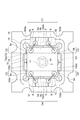
- FIG. 2 is a plan view of a part including a Fabry-Perot interference filter, a spacer, and an adhesive member in the light detection device of FIG. 1.
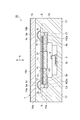
- FIG. 2 is a cross-sectional view of a portion including a Fabry-Perot interference filter, a spacer, and an adhesive member in the light detection device of FIG. 1. It is sectional drawing of the photon detection apparatus of 2nd Embodiment.
- FIG. 6 is a plan view of a portion including a Fabry-Perot interference filter, a third layer substrate, and an adhesive member in the light detection device of FIG. 5. It is sectional drawing of the modification of the photon detection apparatus of 2nd Embodiment.
- the photodetector 1 ⁇ / b> A includes a wiring board 2, a photodetector 3, a plurality of spacers 4, a plurality of adhesive members 5, and a Fabry-Perot interference filter 10.
- the Fabry-Perot interference filter 10 includes a first mirror 31 and a second mirror 41 whose distance is variable.
- the photodetecting device 1A is a spectroscopic sensor that can obtain a spectroscopic spectrum. That is, in the light detection device 1A, when light is incident on the light transmission region 11 of the Fabry-Perot interference filter 10 from the outside, a predetermined value is determined according to the distance between the first mirror 31 and the second mirror 41 in the light transmission region 11. Light having a wavelength is selectively transmitted, and the light transmitted through the light transmission region 11 of the Fabry-Perot interference filter 10 is detected by the photodetector 3.
- the wiring board 2 is mounted with a photodetector 3 and temperature compensation elements (not shown) such as a thermistor.
- a substrate material of the wiring substrate 2 for example, silicon, ceramic, quartz, glass, plastic, or the like can be used.
- the photodetector 3 includes a light receiving unit 3 a that receives light transmitted through the light transmission region 11 of the Fabry-Perot interference filter 10.
- the light transmission region 11 and the light receiving unit 3a face each other in the direction A in which light passes through the light transmission region 11.
- an infrared detector can be used.
- the infrared detector for example, a quantum sensor using InGaAs or the like, a thermal sensor using a thermopile or a bolometer, or the like can be used.
- a silicon photodiode when detecting light in each wavelength region of ultraviolet, visible, and near infrared, for example, a silicon photodiode can be used as the photodetector 3.
- the light detector 3 may be provided with one light receiving part 3a, or a plurality of light receiving parts 3a may be provided in an array.
- a plurality of photodetectors 3 may be mounted on the wiring board 2.
- the plurality of spacers 4 are fixed on the wiring board 2 by an adhesive member (not shown).
- the Fabry-Perot interference filter 10 is fixed on the plurality of spacers 4 by an adhesive member 5.
- the plurality of spacers 4 function as support members that support the Fabry-Perot interference filter 10 on the wiring board 2.
- the photodetector 3 is disposed in a space formed between the wiring board 2 and the Fabry-Perot interference filter 10 by a plurality of spacers 4.
- As a material of each spacer 4 for example, silicon, ceramic, quartz, glass, plastic, or the like can be used.
- each spacer 4 has the same thermal expansion coefficient as compared with the material of the Fabry-Perot interference filter 10. It is preferable that the wiring board 2 and the spacer 4 may be formed integrally.
- the Fabry-Perot interference filter 10 may be supported by one spacer 4 instead of the plurality of spacers 4.
- the material of the adhesive member 5 that bonds the Fabry-Perot interference filter 10 and each spacer 4 is a resin material having flexibility (for example, a resin material such as silicone, urethane, epoxy, acrylic, and hybrid). And may be conductive or non-conductive).
- the resin material is preferably selected from materials having a Young's modulus of less than 1000 MPa, and more preferably selected from materials having a Young's modulus of less than 10 MPa.
- the resin material is preferably selected from materials whose glass transition temperature deviates from the use environment temperature of the photodetecting device 1A.
- the Young's modulus after curing is less than 10 MPa
- the glass transition temperature is the use environment temperature (for example, about 5 to 40 ° C.)
- the lower temperature is about ⁇ 50 to ⁇ 40 ° C.
- the elastic modulus of the adhesive member 5 that bonds the Fabry-Perot interference filter 10 and each spacer 4 is smaller than the elastic modulus of the spacer 4.
- the elastic modulus of the adhesive member 5 that bonds the Fabry-Perot interference filter 10 and each spacer 4 is smaller than the elastic modulus of the adhesive member (not shown) that bonds the wiring board 2 and each spacer 4.
- the Young's modulus after curing becomes 100 MPa or more.
- the spacer 4 has a Young's modulus of 100 GPa or more when it is made of silicon, 100 GPa or more when it is made of ceramic, 10 GPa or more (typically 70 to 80 GPa) when it is made of glass, and when it is made of plastic. Becomes 0.1 GPa or more.
- the elastic modulus means Young's modulus (longitudinal elastic modulus: relationship of strain to tensile / compressive stress), transverse elastic modulus (relationship of strain to shear stress), and bulk modulus (pressure and volume strain under uniform compression). Relationship). That is, Young's modulus is a specific example of elastic modulus.
- the light detection apparatus 1A further includes a CAN package 6.
- the CAN package 6 accommodates the above-described wiring board 2, photodetector 3, temperature compensation element (not shown), a plurality of spacers 4, a plurality of adhesive members 5, and a Fabry-Perot interference filter 10.
- the CAN package 6 has a stem 61 and a cap 62.
- the cap 62 is provided with an opening 62a, and a plate-like light transmitting member 63 is fixed to the opening 62a from the inside.
- the light transmission region 11 and the opening 62a face each other in the direction A.
- the light transmission member 63 As a material of the light transmission member 63, a material (for example, glass, silicon, germanium, etc.) corresponding to the measurement wavelength range of the light detection device 1A can be used. In addition, a light reflection preventing layer may be formed on at least one of the front and back surfaces of the light transmitting member 63. In addition, a band pass filter that transmits only light in the measurement wavelength range may be used as the light transmitting member 63.
- the wiring board 2 is fixed to the stem 61.
- the electrode pads provided on the wiring board 2, the terminals of the photodetector 3, the terminals of the temperature compensation element, and the terminals 12 and 13 of the Fabry-Perot interference filter 10 are each of the plurality of lead pins 9 that penetrate the stem 61.
- wire 8 are electrically connected. Thereby, input / output of electric signals to / from each of the photodetector 3, the temperature compensating element, and the Fabry-Perot interference filter 10 is possible.
- the spacer 4 is disposed immediately below the terminals 12 and 13 of the Fabry-Perot interference filter 10, wire bonding can be reliably performed.
- the first mirror in the light transmission region 11 of the Fabry-Perot interference filter 10 when light enters the light transmission region 11 of the Fabry-Perot interference filter 10 from the outside via the opening 62a and the light transmission member 63, the first mirror in the light transmission region 11 Depending on the distance between the first mirror 31 and the second mirror 41, light having a predetermined wavelength is selectively transmitted.
- the light transmitted through the first mirror 31 and the second mirror 41 is incident on the light receiving unit 3 a of the photodetector 3 and is detected by the photodetector 3.
- the first mirror 31 and the second mirror 41 are moved while changing the voltage applied to the Fabry-Perot interference filter 10 (that is, changing the distance between the first mirror 31 and the second mirror 41).
- a spectrum can be obtained by detecting the transmitted light with the photodetector 3.
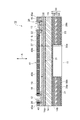
- the Fabry-Perot interference filter 10 includes a substrate 14. On the light incident side surface 14 a of the substrate 14, the antireflection layer 15, the first stacked body 30, the sacrificial layer 16, and the second stacked body 40 are stacked in this order. A gap (air gap) S is formed by the frame-shaped sacrificial layer 16 between the first stacked body 30 and the second stacked body 40.
- the Fabry-Perot interference filter 10 light is incident on the second stacked body 40 from the opposite side of the substrate 14. The light having a predetermined wavelength passes through the light transmission region 11 defined at the center of the Fabry-Perot interference filter 10.
- the substrate 14 is made of, for example, silicon, quartz, glass or the like.
- the antireflection layer 15 and the sacrificial layer 16 are made of, for example, silicon oxide.
- the thickness of the sacrificial layer 16 is preferably an integral multiple of 1/2 of the center transmission wavelength (that is, the center wavelength of the wavelength range that the Fabry-Perot interference filter 10 can transmit).
- the part corresponding to the light transmission region 11 in the first stacked body 30 functions as the first mirror 31.
- the first stacked body 30 is configured by alternately stacking a plurality of polysilicon layers and a plurality of silicon nitride layers one by one.
- the optical thickness of each of the polysilicon layer and the silicon nitride layer constituting the first mirror 31 is preferably an integral multiple of 1/4 of the center transmission wavelength. Note that a silicon oxide layer may be used instead of the silicon nitride layer.
- the portion of the second stacked body 40 corresponding to the light transmission region 11 functions as the second mirror 41 that faces the first mirror 31 with the gap S therebetween.
- the second stacked body 40 is configured by alternately stacking a plurality of polysilicon layers and a plurality of silicon nitride layers one by one.
- the optical thickness of each of the polysilicon layer and the silicon nitride layer constituting the second mirror 41 is preferably an integral multiple of 1/4 of the center transmission wavelength. Note that a silicon oxide layer may be used instead of the silicon nitride layer.
- a plurality of through holes 40b extending from the surface 40a of the second stacked body 40 to the space S are provided in a portion corresponding to the space S in the second stacked body 40 so as to be uniformly distributed.
- the plurality of through holes 40b are formed to such an extent that the function of the second mirror 41 is not substantially affected.
- the inner diameter of each through hole 40b is 100 nm to 5 ⁇ m. Further, the opening area of the plurality of through holes 40 b occupies 0.01 to 10% of the area of the second mirror 41.
- the first mirror 31 and the second mirror 41 are supported by the substrate 14.
- the first mirror 31 is disposed on the light incident side of the substrate 14.
- the second mirror 41 is disposed on the light incident side of the first mirror 31 with the gap S therebetween.
- a first electrode 17 is formed on the first mirror 31 so as to surround the light transmission region 11. Further, the second electrode 18 is formed on the first mirror 31 so as to include the light transmission region 11.
- the first electrode 17 and the second electrode 18 are formed by doping the polysilicon layer with impurities to reduce the resistance.
- the size of the second electrode 18 is preferably a size including the entire light transmission region 11, but may be substantially the same as the size of the light transmission region 11.
- the third electrode 19 is formed on the second mirror 41.
- the third electrode 19 faces the first electrode 17 and the second electrode 18 with the gap S in the direction A.
- the third electrode 19 is formed by doping the polysilicon layer with impurities to reduce the resistance.
- the second electrode 18 is located on the opposite side of the third electrode 19 with respect to the first electrode 17 in the direction A. That is, the first electrode 17 and the second electrode 18 are not arranged on the same plane in the first mirror 31. The second electrode 18 is farther from the third electrode 19 than the first electrode 17.
- the terminal 12 is for applying a voltage to the Fabry-Perot interference filter 10.
- a pair of terminals 12 are provided so as to face each other with the light transmission region 11 in between.
- Each terminal 12 is disposed in a through hole extending from the surface 40 a of the second stacked body 40 to the first stacked body 30.
- Each terminal 12 is electrically connected to the first electrode 17 via the wiring 21.
- the terminal 13 is for applying a voltage to the Fabry-Perot interference filter 10.
- a pair of terminals 13 are provided so as to face each other with the light transmission region 11 in between.
- the direction in which the pair of terminals 12 face each other and the direction in which the pair of terminals 13 face each other are orthogonal.
- Each terminal 13 is electrically connected to the third electrode 19 via the wiring 22.
- the third electrode 19 is also electrically connected to the second electrode 18 through the wiring 23.
- the trenches 26 and 27 are provided on the surface 30 a of the first stacked body 30.
- the trench 26 extends in an annular shape so as to surround the wiring 23 extending in the direction A from the terminal 13.
- the trench 26 electrically insulates the first electrode 17 and the wiring 23.
- the trench 27 extends in a ring shape along the inner edge of the first electrode 17.
- the trench 27 electrically insulates the first electrode 17 and a region inside the first electrode 17.
- the region in each of the trenches 26 and 27 may be an insulating material or a gap.
- a trench 28 is provided on the surface 40 a of the second stacked body 40.
- the trench 28 extends in an annular shape so as to surround the terminal 12.
- the bottom surface of the trench 28 reaches the sacrificial layer 16.
- the trench 28 electrically insulates the terminal 12 and the third electrode 19.
- the region in the trench 28 may be an insulating material or a gap.
- An antireflection layer 51, a third laminated body 52, an intermediate layer 53, and a fourth laminated body 54 are laminated in this order on the surface 14b on the light emitting side of the substrate 14.
- the antireflection layer 51 and the intermediate layer 53 have the same configuration as the antireflection layer 15 and the sacrificial layer 16, respectively.
- the third stacked body 52 and the fourth stacked body 54 have a stacked structure that is symmetrical to the first stacked body 30 and the second stacked body 40, respectively, with respect to the substrate 14.
- the antireflection layer 51, the third laminate 52, the intermediate layer 53, and the fourth laminate 54 constitute a laminate 50.
- the stacked body 50 is disposed on the light emitting side of the substrate 14 and has a function of suppressing warpage of the substrate 14.
- a cylindrical opening 50 a is formed in the stacked body 50 so as to include the light transmission region 11.
- the opening 50 a opens to the light emitting side, and the bottom surface of the opening 50 a reaches the antireflection layer 51.
- a light shielding layer 29 a is formed on the surface 50 b on the light emitting side of the stacked body 50.
- the light shielding layer 29a is made of aluminum or the like.
- a protective layer 29b is formed on the surface of the light shielding layer 29a and the inner surface of the opening 50a.
- the protective layer 29b is made of, for example, aluminum oxide. Note that the optical influence of the protective layer 29b can be ignored by setting the thickness of the protective layer 29b to 1 to 100 nm (preferably about 30 nm).
- the Fabry-Perot interference filter 10 configured as described above, when a voltage is applied between the first electrode 17 and the third electrode 19 via the terminals 12 and 13, an electrostatic force corresponding to the voltage is generated. Occurs between the first electrode 17 and the third electrode 19.
- the second mirror 41 is driven by the electrostatic force so as to be attracted to the first mirror 31 fixed to the substrate 14. By this driving, the distance between the first mirror 31 and the second mirror 41 is adjusted.
- the wavelength of light transmitted through the Fabry-Perot interference filter 10 depends on the distance between the first mirror 31 and the second mirror 41 in the light transmission region 11. Therefore, by adjusting the voltage applied between the first electrode 17 and the third electrode 19, the wavelength of the transmitted light can be appropriately selected.
- the second electrode 18 has the same potential as the electrically connected third electrode 19. Therefore, the second electrode 18 functions as a compensation electrode for keeping the first mirror 31 and the second mirror 41 flat in the light transmission region 11.
- the configuration of the adhesive member 5 will be described in more detail with reference to FIGS.
- the wire 8, the stem 61, etc. are omitted, and in FIG. 4, the wiring board 2, the wire 8, the stem 61, etc. are omitted.
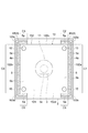
- the Fabry-Perot interference filter 10 is supported by a pair of spacers 4A and 4B.
- On the placement surface 4a of one spacer 4A a portion of the bottom surface 101 of the Fabry-Perot interference filter 10 that is outside the light transmission region 11 and along the side surface 102a of the Fabry-Perot interference filter 10 is placed.
- On the placement surface 4a of the other spacer 4B a portion of the bottom surface 101 of the Fabry-Perot interference filter 10 that is outside the light transmission region 11 and along the side surface 102b of the Fabry-Perot interference filter 10 is placed. Has been.
- the Fabry-Perot interference filter 10 has a rectangular side surface 102 when viewed from the direction A.
- the side surface (first side surface, second side surface) 102 a and the side surface (first side surface, third side surface) 102 b face each other with the light transmission region 11 in between.
- the side surface 102a is positioned on the mounting surface 4a of the spacer 4A so that a part of the mounting surface 4a of the spacer 4A is disposed outside the side surface 102a (outside of the side surface 102 when viewed from the direction A). ing. As a result, the corner C1 (side surface 102a) is formed between the side surface 102a and a portion of the mounting surface 4a of the spacer 4A that is outside the side surface 102a (portion exposed without the Fabry-Perot interference filter 10 being mounted). And a space at an end where the mounting surface 4a of the spacer 4A intersects).
- One end of the side surface (fifth side surface) 102c that forms the corner portion 103a together with the side surface (fourth side surface) 102a of the side surface 102 is on the corner portion 103a side, and part of the mounting surface 4a of the spacer 4A is outside the side surface 102c. It is located on the mounting surface 4a of the spacer 4A.
- a corner C2 (a space at an end where the side surface 102c and a part of the mounting surface 4a of the spacer 4A intersect) is formed.
- One end of the side surface (fifth side surface) 102d forming the corner portion 103b together with the side surface (fourth side surface) 102a of the side surface 102 is on the corner portion 103b side, and a part of the mounting surface 4a of the spacer 4A is outside the side surface 102d.
- a corner C3 (a space at an end where the side surface 102d and a part of the mounting surface 4a of the spacer 4A intersect) is formed. Note that the above-described one end of the side surface 102a, side surface 102c, and one end portion of the side surface 102d correspond to part of the outer edge of the Fabry-Perot interference filter 10 when viewed from the direction A.
- the side surface 102b is located on the mounting surface 4a of the spacer 4B so that a part of the mounting surface 4a of the spacer 4B is disposed outside the side surface 102b.
- the corner C4 (side surface 102b) is formed between the side surface 102b and the portion of the mounting surface 4a of the spacer 4B that is outside the side surface 102b (the portion that is exposed without the Fabry-Perot interference filter 10 being mounted). And a space at an end where the mounting surface 4a of the spacer 4B intersects).
- the other end portion on the corner portion 103c side of the side surface (fifth side surface) 102c that forms the corner portion 103c together with the side surface (fourth side surface) 102b is part of the mounting surface 4a of the spacer 4B. It is located on the mounting surface 4a of the spacer 4B so as to be arranged outside.
- the other end of the side surface 102c and a portion outside the other end of the side surface 102c of the mounting surface 4a of the spacer 4B (a portion that is exposed without being mounted with the Fabry-Perot interference filter 10).
- a corner C5 (a space at an end where the side surface 102c and a part of the mounting surface 4a of the spacer 4B intersect) is formed.
- the other end portion on the corner portion 103d side of the side surface (fifth side surface) 102d that forms the corner portion 103d together with the side surface (fourth side surface) 102b is part of the mounting surface 4a of the spacer 4B. It is located on the mounting surface 4a of the spacer 4B so as to be arranged outside.
- a corner C6 (a space at an end where the side surface 102d and a part of the mounting surface 4a of the spacer 4B intersect) is formed.
- the side surface 102b, the other end portion of the side surface 102c, and the other end portion of the side surface 102d correspond to part of the outer edge of the Fabry-Perot interference filter 10 when viewed from the direction A.
- adhesive members 5 are arranged at the corners C1, C2, C3, and the adhesive members 5 arranged at the corners C1, C2, C3 are continuous with each other. . That is, the adhesive member 5 arranged on the mounting surface 4a of the spacer 4A is continuous over the entire corner C1, and covers the corners 103a and 103b from the outside.
- the adhesive members 5 are arranged at the corners C4, C5, C6, and the adhesive members 5 arranged at the corners C4, C5, C6 are continuous with each other. . That is, the adhesive member 5 disposed on the placement surface 4a of the spacer 4B is continuous over the entire corner C4 and covers the corners 103c and 103d from the outside.
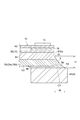
- the adhesive member 5 disposed on the mounting surface 4a of the spacer 4A includes a first portion 5a and a second portion 5b.
- the 1st part 5a is a part arrange
- the second portion 5 b is a portion disposed between the placement surface 4 a of the spacer 4 ⁇ / b> A and the bottom surface 101 of the Fabry-Perot interference filter 10.
- the first portion 5a is in contact with the side surface 102a and the placement surface 4a of the spacer 4A.
- the first portion 5a is in contact with one end portion of the side surface 102c and the placement surface 4a of the spacer 4A.
- the first portion 5a is in contact with one end portion of the side surface 102d and the placement surface 4a of the spacer 4A. That is, the adhesive member 5 arranged on the placement surface 4a of the spacer 4A is in contact with the side surface 102 and the placement surface 4a of the spacer 4A.
- the adhesive member 5 disposed on the placement surface 4a of the spacer 4B includes a first portion 5a and a second portion 5b.
- the 1st part 5a is a part arrange
- the second portion 5 b is a portion disposed between the placement surface 4 a of the spacer 4 B and the bottom surface 101 of the Fabry-Perot interference filter 10.
- the first portion 5a is in contact with the side surface 102b and the placement surface 4a of the spacer 4B.
- the first portion 5a is in contact with the other end portion of the side surface 102c and the placement surface 4a of the spacer 4B.
- the first portion 5a is in contact with the other end portion of the side surface 102d and the placement surface 4a of the spacer 4B. That is, the adhesive member 5 disposed on the placement surface 4a of the spacer 4B is in contact with the side surface 102 and the placement surface 4a of the spacer 4B.
- each corner C1, C2, C3, the highest edge 5c of the first portion 5a reaches the side surface of the substrate 14 of the Fabry-Perot interference filter 10. That is, the adhesive member 5 disposed on the placement surface 4 a of the spacer 4 ⁇ / b> A is in contact with the substrate 14 on the side surface 102.
- the highest edge 5c of the first portion 5a reaches the side surface of the substrate 14 of the Fabry-Perot interference filter 10. That is, the adhesive member 5 disposed on the placement surface 4 a of the spacer 4 B is in contact with the substrate 14 on the side surface 102.
- the height H of the first portion 5a in the direction perpendicular to the mounting surface 4a of each spacer 4A, 4B and the width W of the first portion 5a in the direction perpendicular to the side surface 102 of the Fabry-Perot interference filter 10 are: Each of them is 10 to 1000 ⁇ m.
- the thickness of the Fabry-Perot interference filter 10 is 100 to 1000 ⁇ m.
- the width of the portion of the mounting surface 4a that protrudes to the outside of the side surface 102 (the width in the direction perpendicular to the side surface 102) is 10 to 1000 ⁇ m.
- the height H of the first portion 5 a is preferably 1/10 or more of the thickness of the Fabry-Perot interference filter 10 and less than the thickness of the Fabry-Perot interference filter 10.
- the distance between the bottom surface 101 and the surface 14 b on the light emitting side of the substrate 14 is 0.1 to 10 ⁇ m. Therefore, if the height H of the first portion 5 a is 10 ⁇ m or more, The highest edge portion 5 c of the one portion 5 a can reach the side surface of the substrate 14 of the Fabry-Perot interference filter 10.
- a value obtained by subtracting the thickness of the second portion 5b in the direction perpendicular to the placement surface 4a from the height H of the first portion 5a in the direction perpendicular to the placement surface 4a (Fabry-Perot interference). (Corresponding to the height of the edge portion 5c from the bottom surface 101 of the filter 10) is larger than the thickness of the second portion 5b in the direction perpendicular to the mounting surface 4a.
- the adhesive member 5 having an elastic modulus smaller than the elastic modulus of each of the spacers 4A and 4B is disposed at the corners C1, C2, C3, C4, C5, and C6, and the Fabry-Perot interference filter
- the side surface 102 and each part of the mounting surface 4a of each spacer 4A, 4B are in contact with each other.
- the adhesive member 5 is merely interposed between the bottom surface 101 of the Fabry-Perot interference filter 10 and the mounting surface 4a of each spacer 4A, 4B, the Fabry-Perot interference filter 10 and the light It occurs in the Fabry-Perot interference filter 10 due to a difference in thermal expansion coefficient with other members (not only the spacers 4A and 4B but also the wiring board 2, the stem 61, the cap 62, etc.) constituting the detection device 1A. Stress can be sufficiently absorbed by the adhesive member 5.
- the Fabry-Perot interference filter 10 is more stable than the case where the adhesive member 5 is merely interposed between the bottom surface 101 of the Fabry-Perot interference filter 10 and the mounting surface 4a of each spacer 4A, 4B. In this state, it can be held on the spacers 4A and 4B more firmly. Therefore, according to the photodetector 1A, the temperature characteristic of the transmission wavelength in the Fabry-Perot interference filter 10 can be sufficiently improved, and the holding state of the Fabry-Perot interference filter 10 on the spacers 4A and 4B can be stabilized. it can.
- the adhesive member 5 is smaller than the elastic modulus of other members (not only the spacers 4A and 4B but also the Fabry-Perot interference filter 10, the wiring board 2, the stem 61, the cap 62, etc.) constituting the light detection device 1A. It preferably has an elastic modulus.
- the Fabry-Perot interference filter 10 and the light detection device 1A are configured by the second portion 5b being interposed between the mounting surfaces 4a of the spacers 4A and 4B and the bottom surface 101 of the Fabry-Perot interference filter 10.
- the stress generated in the Fabry-Perot interference filter 10 due to the difference in thermal expansion coefficient with other members is absorbed, and as a result, the generation of stress in the Fabry-Perot interference filter 10 is suppressed.
- thermal stress generated in the CAN package 6 increases, thermal stress generated from various areas and directions. Can be sufficiently recovered (amount of thermal stress absorbed by the adhesive member 5> amount of thermal stress generated in the CAN package 6), the temperature characteristic of the transmission wavelength in the Fabry-Perot interference filter 10 is improved.
- the first portions 5a arranged at the corners C1, C2, C3, C4, C5, and C6 are formed in a fillet shape so as to scoop up the side surface 102 of the Fabry-Perot interference filter 10, each spacer 4A , 4B and the bottom surface 101 of the Fabry-Perot interference filter 10, the Fabry-Perot interference filter 10 is held from the outside of the side surface 102. Therefore, the holding state of the Fabry-Perot interference filter 10 on the spacers 4A and 4B is stabilized.
- the structure of the adhesive member 5 in the light detection device 1A is improved in the temperature characteristic of the transmission wavelength in the Fabry-Perot interference filter 10, and in the stabilization of the holding state of the Fabry-Perot interference filter 10 on the spacers 4A and 4B. It is possible to achieve both.
- the adhesive member 5 a value obtained by subtracting the thickness of the second portion 5b in the direction perpendicular to the placement surface 4a from the height H of the first portion 5a in the direction perpendicular to the placement surface 4a. It is larger than the thickness of the second portion 5b in the direction perpendicular to the surface 4a.
- the adhesive member 5 more fully absorbs the stress generated in the Fabry-Perot interference filter 10 due to the difference in thermal expansion coefficient between the Fabry-Perot interference filter 10 and the other members constituting the light detection device 1A. be able to.
- the width W of the first portion 5a in the direction perpendicular to the side surface 102 of the Fabry-Perot interference filter 10 is larger than the height H of the first portion 5a in the direction perpendicular to the placement surface 4a of each spacer 4A, 4B. Then, it is possible to more surely realize both the improvement of the temperature characteristic of the transmission wavelength in the Fabry-Perot interference filter 10 and the stabilization of the holding state of the Fabry-Perot interference filter 10 on the spacers 4A and 4B. Therefore, it is preferable that the adhesive member 5 is in contact with the entire width of the portion of the mounting surface 4a that protrudes outside the side surface 102.
- the adhesive members 5 arranged at the corners C1, C2, C3, C4, C5, and C6 are in contact with the substrate 14 on the side surface 102 of the Fabry-Perot interference filter 10.
- the adhesive member 5 more fully absorbs the stress generated in the Fabry-Perot interference filter 10 due to the difference in thermal expansion coefficient between the Fabry-Perot interference filter 10 and the other members constituting the light detection device 1A. be able to.
- the substrate 14 that supports the first mirror 31 and the second mirror 41 is held from the outside by the adhesive member 5, the holding state of the Fabry-Perot interference filter 10 can be further stabilized.
- the adhesive member 5 is disposed at the corner C1 so as to be continuous over the entire corner C1 formed by the side surface 102a of the Fabry-Perot interference filter 10, and is attached to the side surface 102a. In contact.
- the adhesive member 5 is disposed at the corner C4 so as to be continuous over the entire corner C4 formed by the side surface 102b of the Fabry-Perot interference filter 10, and is in contact with the side surface 102b.
- the stress generated in the Fabry-Perot interference filter 10 due to the difference in thermal expansion coefficient between the Fabry-Perot interference filter 10 and the other members constituting the light detection device 1A is uniformly absorbed by the adhesive member 5. be able to.
- an adhesive member 5 is formed as follows. That is, an adhesive containing, for example, a silicone-based resin material is applied to the mounting surface 4a of each spacer 4A, 4B with a uniform thickness, and the Fabry-Perot interference filter 10 is mounted thereon, and in that state For example, the adhesive is thermally cured. When the Fabry-Perot interference filter 10 is placed, the adhesive that exists between the placement surface 4 a of each spacer 4 A and 4 B and the bottom surface 101 of the Fabry-Perot interference filter 10 is uniform due to its own weight.
- the adhesive present in the corners C1, C2, C3, C4, C5, and C6 scoops up the side surface 102 of the Fabry-Perot interference filter 10 and has a uniform height and width. In this way, the adhesive member 5 including the first portion 5a having a uniform height H and width W is formed.
- a Fabry-Perot interference filter 10 is placed on the placement surface 4a of each spacer 4A, 4B, and then an adhesive containing, for example, a silicone-based resin material is added to the corners C1, C2, C3, C4, C5. It may be applied along C6 with a uniform thickness, after which the adhesive may be heat cured, for example. Also in this case, when the adhesive is applied along the corners C1, C2, C3, C4, C5, C6, the mounting surface 4a of each spacer 4A, 4B and the bottom surface 101 of the Fabry-Perot interference filter 10 An adhesive enters between them, and the adhesive has a uniform thickness due to the weight of the Fabry-Perot interference filter 10.
- an adhesive containing, for example, a silicone-based resin material is added to the corners C1, C2, C3, C4, C5. It may be applied along C6 with a uniform thickness, after which the adhesive may be heat cured, for example. Also in this case, when the adhesive is applied along the corners C1, C2, C3, C4, C
- the adhesive present in the corners C1, C2, C3, C4, C5, and C6 scoops up the side surface 102 of the Fabry-Perot interference filter 10 and has a uniform height and width.
- an adhesive containing, for example, a silicone-based resin material is applied only to a region where the bottom surface 101 of the Fabry-Perot interference filter 10 is placed on the placement surface 4a of each spacer 4A, 4B, and then the Fabry-Perot The interference filter 10 is placed, and then the adhesive is thermally cured, for example, and then the adhesive including, for example, a silicone-based resin material is uniformly distributed along the corners C1, C2, C3, C4, C5, and C6.
- the adhesive may be applied with a sufficient thickness, and then the adhesive may be thermally cured, for example. Also in this case, when the Fabry-Perot interference filter 10 is placed, the adhesive existing between the placement surfaces 4a of the spacers 4A and 4B and the bottom surface 101 of the Fabry-Perot interference filter 10 is the Fabry-Perot interference filter. It becomes a uniform thickness by its own weight of 10. Further, the adhesive present in the corners C1, C2, C3, C4, C5, and C6 has a uniform height and width on the side surface 102 of the Fabry-Perot interference filter 10.
- the adhesive member 5 is disposed at the corner C1 formed by the side surface 102a of the Fabry-Perot interference filter 10, and is in contact with the side surface 102a. Further, the adhesive member 5 is disposed at a corner C4 formed by the side surface 102b of the Fabry-Perot interference filter 10 facing the side surface 102a with the light transmission region 11 interposed therebetween, and is in contact with the side surface 102b. As a result, the Fabry-Perot interference filter 10 can be held on the spacers 4A and 4B in a more stable state.
- the side surfaces 102a and 102b facing each other are used. Even if the adhesive member 5 is disposed in each of the corners C1 and C4 formed by each, distortion of the Fabry-Perot interference filter 10 due to the thermal stress generated in the CAN package 6 is suppressed. The thermal stress generated in the package 6 is absorbed by the adhesive member 5.
- the adhesive members 5 arranged at the corners C1, C2, and C3 are continuous with each other and cover the corners 103a and 103b of the Fabry-Perot interference filter 10 from the outside.
- the adhesive members 5 arranged at the corners C4, C5, and C6 are continuous with each other and cover the corners 103c and 103d of the Fabry-Perot interference filter 10 from the outside.
- the corners 103a, 103b, where stress generated in the Fabry-Perot interference filter 10 due to a difference in thermal expansion coefficient between the Fabry-Perot interference filter 10 and other members constituting the light detection device 1A is likely to concentrate.
- the stress can be sufficiently absorbed by the adhesive member 5.
- the adhesive member 5 is not provided on the entire bottom surface 101 of the Fabry-Perot interference filter 10 (particularly, since the adhesive member 5 is not provided in the light transmission region 11), the following effects are obtained. Played. That is, since the light transmitted through the Fabry-Perot interference filter 10 does not pass through the adhesive member 5, it is not necessary to select the adhesive member 5 having a high light transmittance, and the degree of freedom in selecting the adhesive member 5 is improved.
- the light that has passed through the Fabry-Perot interference filter 10 does not pass through the adhesive member 5, the light that passes through the Fabry-Perot interference filter 10 has optical characteristics (refractive index, transmittance, etc.) of the adhesive member 5 as the ambient temperature changes. ) Is not affected by changes. Further, the Fabry-Perot interference filter 10 is distorted or tilted due to the shrinkage of the adhesive member 5 at the time of curing and the stress generated by the expansion and contraction of the adhesive member 5 due to the change in ambient temperature at the time of use. It is suppressed. [Second Embodiment] [Configuration of photodetection device]
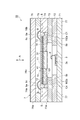
- the light detection device 1B is different from the light detection device 1A described above in that it is configured as an SMD (Surface Mount Device).
- the light detection apparatus 1B includes an SMD package 7 that houses a light detector 3, a temperature compensation element (not shown), and a Fabry-Perot interference filter 10.
- the SMD package 7 includes a first layer substrate 71, a second layer substrate 72, a third layer substrate 73, a fourth layer substrate 74, a fifth layer substrate 75, and a sixth layer substrate 76.
- the first layer substrate 71, the second layer substrate 72, the third layer substrate 73, the fourth layer substrate 74, the fifth layer substrate 75, and the sixth layer substrate 76 are laminated in this order.
- An opening is provided in the center of each of the second layer substrate 72, the third layer substrate 73, the fourth layer substrate 74, and the fifth layer substrate 75.
- the opening of the third layer substrate 73 includes the opening of the second layer substrate 72.
- the opening of the fourth layer substrate 74 includes the opening of the third layer substrate 73.
- the opening of the fifth layer substrate 75 includes the opening of the fourth layer substrate 74.
- the photodetector 3 and a temperature compensation element are mounted on the exposed surface of the first layer substrate 71.
- a plurality of electrode pads 77 are provided on the back surface of the first layer substrate 71.
- Each terminal of the photodetector 3 and each terminal of the temperature compensating element are connected to the electrode pad 77 by wiring provided on the first layer substrate 71 or by wiring provided on the wire 8 and each substrate 71, 72. And are electrically connected.
- the Fabry-Perot interference filter 10 is fixed to the exposed surface of the third layer substrate 73 by the adhesive member 5.
- the upper surfaces of the terminals 12 and 13 of the Fabry-Perot interference filter 10 are at the same height as the upper surface of the fourth layer substrate 74.
- Pads electrically connected to the electrode pads 77 are provided on the upper surface of the fourth layer substrate 74, and the terminals 12 and 13 are connected to the pads on the upper surface of the fourth layer substrate 74 by the wires 8. Yes.
- Each terminal 12, 13 of the Fabry-Perot interference filter 10 is electrically connected to the electrode pad 77 by the wire 8 and the wiring provided on each substrate 71, 72, 73, 74.
- the third layer substrate 73 functions as a support member that supports the Fabry-Perot interference filter 10 on the first layer substrate 71 and the second layer substrate 72.
- the material of the first layer substrate 71, the second layer substrate 72, the third layer substrate 73, the fourth layer substrate 74, and the fifth layer substrate 75 for example, ceramic, resin, or the like can be used.
- the material of the third layer substrate 73 is less than the material of the Fabry-Perot interference filter 10. It is preferable that the expansion coefficients are equivalent.
- a flexible resin material for example, a resin material such as silicone, urethane, epoxy, acrylic, hybrid, etc.
- the resin material is preferably selected from materials having a Young's modulus of less than 1000 MPa, and more preferably selected from materials having a Young's modulus of less than 10 MPa.
- the resin material is selected from materials whose glass transition temperature deviates from the use environment temperature of the light detection device 1B.
- the Young's modulus after curing is less than 10 MPa
- the glass transition temperature is the use environment temperature (for example, about 5 to 40 ° C.)
- the lower temperature is about ⁇ 50 to ⁇ 40 ° C.
- the elastic modulus of the adhesive member 5 that bonds the Fabry-Perot interference filter 10 and the third layer substrate 73 is smaller than the elastic modulus of the third layer substrate 73.
- the elastic modulus of the adhesive member 5 that bonds the Fabry-Perot interference filter 10 and the third layer substrate 73 is determined by the first layer substrate 71, the second layer substrate 72, the third layer substrate 73, the fourth layer substrate 74, It is smaller than the elastic modulus of an adhesive member (not shown) that bonds the 5-layer substrate 75 and the sixth-layer substrate 76 together.
- an epoxy-based material is used as a material of an adhesive member for bonding the first layer substrate 71, the second layer substrate 72, the third layer substrate 73, the fourth layer substrate 74, the fifth layer substrate 75, and the sixth layer substrate 76. If an adhesive containing a resin material is used, the Young's modulus after curing is 100 MPa or more.
- the sixth layer substrate 76 includes a light transmission substrate 76a and a light shielding layer 76b.
- the light transmission substrate 76a is fixed on the fifth layer substrate 75 by an adhesive member (not shown).
- a material of the light transmission substrate 76a a material (for example, glass, silicon, germanium, etc.) corresponding to the measurement wavelength range of the light detection device 1B can be used.
- the light shielding layer 76b is formed on the surface of the light transmission substrate 76a.
- a light shielding material or a light absorbing material for example, a metal such as aluminum, a metal oxide such as chromium oxide, a black resin, or the like.
- An opening 76c is provided in the light shielding layer 76b.
- the light transmission region 11 and the opening 76c face each other in the direction A.
- the light shielding layer 76b may be formed on the back surface of the light transmission substrate 76a.
- a light reflection preventing layer may be formed on at least one of the front and back surfaces of the light transmission substrate 76a.
- a band pass filter that transmits only light in the measurement wavelength range may be used as the light transmitting substrate 76a.
- the first mirror in the light transmission region 11 of the Fabry-Perot interference filter 10 when light enters the light transmission region 11 of the Fabry-Perot interference filter 10 from the outside via the opening 76c and the light transmission substrate 76a, the first mirror in the light transmission region 11 Depending on the distance between the first mirror 31 and the second mirror 41, light having a predetermined wavelength is selectively transmitted.
- the light transmitted through the first mirror 31 and the second mirror 41 is incident on the light receiving unit 3 a of the photodetector 3 and is detected by the photodetector 3.
- the first mirror 31 and the second mirror 41 are moved while changing the voltage applied to the Fabry-Perot interference filter 10 (that is, changing the distance between the first mirror 31 and the second mirror 41).
- a spectrum can be obtained by detecting the transmitted light with the photodetector 3.
- the configuration of the adhesive member 5 will be described in more detail with reference to FIGS.
- the sixth layer substrate 76 and the like are omitted.
- the mounting surface 73 a of the third layer substrate 73 is a part of the bottom surface 101 of the Fabry-Perot interference filter 10 that is outside the light transmission region 11 and has Fabry-Perot interference. A portion along the side surface 102 of the filter 10 is placed.
- the Fabry-Perot interference filter 10 has a rectangular side surface 102 when viewed from the direction A. Of the side surfaces 102, the side surface (first side surface, second side surface) 102 a and the side surface (first side surface, third side surface) 102 b face each other with the light transmission region 11 in between.
- the side surface 102a is located on the mounting surface 73a so that a part of the mounting surface 73a is disposed outside the side surface 102a (outside the side surface 102 when viewed from the direction A).
- a corner C1 is formed by the side surface 102a and a portion of the placement surface 73a outside the side surface 102a (a portion that is exposed without the Fabry-Perot interference filter 10 being placed).
- One end of the side surface (fifth side surface) 102c that forms the corner portion 103a together with the side surface (fourth side surface) 102a of the side surface 102 on the corner portion 103a side is partly placed on the outside of the side surface 102c. As described above, it is located on the mounting surface 73a.
- a corner C2 is formed between one end portion of the side surface 102c and a portion of the placement surface 73a outside the one end portion of the side surface 102c (a portion exposed without the Fabry-Perot interference filter 10 being placed). Is formed.
- One end of the side surface (fifth side surface) 102d that forms the corner portion 103b together with the side surface (fourth side surface) 102a of the side surface 102 on the corner portion 103b side is partly placed on the outside of the side surface 102d. As described above, it is located on the mounting surface 73a.
- a corner C3 is formed between one end portion of the side surface 102d and a portion of the placement surface 73a outside the one end portion of the side surface 102d (a portion that is exposed without the Fabry-Perot interference filter 10 being placed). Is formed. Note that the above-described one end of the side surface 102a, side surface 102c, and one end portion of the side surface 102d correspond to part of the outer edge of the Fabry-Perot interference filter 10 when viewed from the direction A.
- the side surface 102b is located on the mounting surface 73a so that a part of the mounting surface 73a is disposed outside the side surface 102b.
- a corner C4 is formed by the side surface 102b and a portion of the placement surface 73a outside the side surface 102b (a portion that is exposed without the Fabry-Perot interference filter 10 being placed).
- the other end portion of the side surface (fifth side surface) 102c that forms the corner portion 103c together with the side surface (fourth side surface) 102b is disposed on the outer side of the side surface 102c. As described above, it is located on the placement surface 73a.
- a corner is formed between the other end of the side surface 102c and a portion of the mounting surface 73a outside the other end of the side surface 102c (a portion where the Fabry-Perot interference filter 10 is not mounted and exposed).
- Part C5 is formed.
- the other end portion on the side of the corner portion 103d of the side surface (fifth side surface) 102d that forms the corner portion 103d together with the side surface (fourth side surface) 102b is partly placed on the outside of the side surface 102d. As described above, it is located on the placement surface 73a.
- a corner is formed between the other end of the side surface 102d and a portion of the mounting surface 73a outside the other end of the side surface 102d (a portion where the Fabry-Perot interference filter 10 is not mounted and exposed).
- Part C6 is formed.
- the side surface 102b, the other end portion of the side surface 102c, and the other end portion of the side surface 102d correspond to part of the outer edge of the Fabry-Perot interference filter 10 when viewed from the direction A.
- the adhesive member 5 is disposed at each corner C1, C2, C3.
- the adhesive members 5 arranged at the corners C1, C2, C3 are continuous with each other. That is, the adhesive member 5 disposed at each corner C1, C2, C3 is continuous over the entire corner C1, and covers each corner 103a, 103b from the outside.
- the adhesive member 5 is disposed at each corner C4, C5, C6.
- the adhesive members 5 arranged at the corners C4, C5, C6 are continuous with each other. That is, the adhesive member 5 disposed at each corner C4, C5, C6 is continuous over the entire corner C4 and covers each corner 103c, 103d from the outside.
- the adhesive member 5 disposed at each corner C1, C2, C3 includes a first portion 5a and a second portion 5b.
- the 1st part 5a is a part arrange
- the second portion 5 b is a portion disposed between the placement surface 73 a of the third layer substrate 73 and the bottom surface 101 of the Fabry-Perot interference filter 10.
- the first portion 5a is in contact with each of the side surface 102a, the mounting surface 73a, and the inner surface 74a of the opening of the fourth layer substrate 74.
- the first portion 5a is in contact with one end of the side surface 102c, the placement surface 73a, and the inner surface 74a of the opening of the fourth layer substrate 74.
- the first portion 5a is in contact with one end portion of the side surface 102d, the placement surface 73a, and the inner surface 74a of the opening of the fourth layer substrate 74. That is, the adhesive member 5 disposed in each corner C1, C2, C3 is in contact with each of the side surface 102, the mounting surface 73a, and the inner surface 74a of the opening of the fourth layer substrate 74.
- the adhesive member 5 disposed at each corner C4, C5, C6 includes a first portion 5a and a second portion 5b.
- the 1st part 5a is a part arrange
- the second portion 5 b is a portion disposed between the placement surface 73 a of the third layer substrate 73 and the bottom surface 101 of the Fabry-Perot interference filter 10.
- the first portion 5a is in contact with each of the side surface 102b, the mounting surface 73a, and the inner surface 74a of the opening of the fourth layer substrate 74.
- the first portion 5a is in contact with the other end portion of the side surface 102c, the placement surface 73a, and the inner surface 74a of the opening of the fourth layer substrate 74.
- the first portion 5a is in contact with the other end of the side surface 102d, the placement surface 73a, and the inner surface 74a of the opening of the fourth layer substrate 74. That is, the adhesive member 5 disposed at each corner C4, C5, C6 is in contact with each of the side surface 102, the mounting surface 73a, and the inner surface 74a of the opening of the fourth layer substrate 74.
- each corner C1, C2, C3 the edge portion 5c on the side of the highest side surface 102 of the first portion 5a reaches the side surface of the substrate 14 of the Fabry-Perot interference filter 10. That is, the adhesive member 5 disposed in each corner C1, C2, C3 is in contact with the substrate 14 on the side surface 102.
- the edge 5c on the side of the highest side 102 of the first portion 5a reaches the side of the substrate 14 of the Fabry-Perot interference filter 10. That is, the adhesive member 5 disposed in each corner C4, C5, C6 is in contact with the substrate 14 on the side surface 102.
- the height of the edge portion 5 c is lower than the height of the Fabry-Perot interference filter 10 and the fourth layer substrate 74.
- a value obtained by subtracting the thickness of the second portion 5b in the direction perpendicular to the placement surface 73a from the height H of the first portion 5a in the direction perpendicular to the placement surface 73a (Fabry-Perot interference). (Corresponding to the height of the edge portion 5c from the bottom surface 101 of the filter 10) is larger than the thickness of the second portion 5b in the direction perpendicular to the mounting surface 73a.
- the adhesive member 5 having an elastic modulus smaller than the elastic modulus of the third layer substrate 73 is disposed at the corners C1, C2, C3, C4, C5, C6, and the Fabry-Perot interference filter.
- the side surface 102 and the part of the mounting surface 73 a of the third layer substrate 73 are in contact with each other.
- the adhesive member 5 is merely interposed between the bottom surface 101 of the Fabry-Perot interference filter 10 and the mounting surface 73a of the third layer substrate 73, the Fabry-Perot interference filter 10 and the light Other members constituting the detection apparatus 1B (not only the third layer substrate 73 but also the first layer substrate 71, the second layer substrate 72, the fourth layer substrate 74, the fifth layer substrate 75, the sixth layer substrate 76, etc.)
- the adhesive member 5 can sufficiently absorb the stress generated in the Fabry-Perot interference filter 10 due to the difference in thermal expansion coefficient between the adhesive member 5 and the adhesive member 5.
- the Fabry-Perot interference filter 10 is more stable than the case where the adhesive member 5 is merely interposed between the bottom surface 101 of the Fabry-Perot interference filter 10 and the mounting surface 73a of the third layer substrate 73. It can be held on the third layer substrate 73 more firmly in the state. Therefore, according to the photodetector 1B, the temperature characteristic of the transmission wavelength in the Fabry-Perot interference filter 10 can be sufficiently improved, and the holding state of the Fabry-Perot interference filter 10 on the third layer substrate 73 can be stabilized. Can do.
- the adhesive member 5 is another member (not only the third layer substrate 73 but also the Fabry-Perot interference filter 10, the first layer substrate 71, the second layer substrate 72, and the fourth layer substrate 74) constituting the light detection device 1 ⁇ / b> B.
- the fifth layer substrate 75, the sixth layer substrate 76, etc. preferably have a smaller elastic modulus.
- the adhesive member 5 In the adhesive member 5, the value obtained by subtracting the thickness of the second portion 5b in the direction perpendicular to the placement surface 73a from the height H of the first portion 5a in the direction perpendicular to the placement surface 73a. It is larger than the thickness of the second portion 5b in the direction perpendicular to the surface 73a. As a result, the adhesive member 5 more fully absorbs the stress generated in the Fabry-Perot interference filter 10 due to the difference in thermal expansion coefficient between the Fabry-Perot interference filter 10 and the other members constituting the light detection device 1B. be able to.
- the width W of the first portion 5a in the direction perpendicular to the side surface 102 of the Fabry-Perot interference filter 10 is larger than the height H of the first portion 5a in the direction perpendicular to the mounting surface 73a of the third layer substrate 73. Then, it is possible to more reliably realize both the improvement of the temperature characteristic of the transmission wavelength in the Fabry-Perot interference filter 10 and the stabilization of the holding state of the Fabry-Perot interference filter 10 on the third layer substrate 73. Therefore, it is preferable that the adhesive member 5 is in contact with the entire width of the portion of the mounting surface 73a that protrudes outside the side surface 102.
- the adhesive members 5 arranged at the corners C1, C2, C3, C4, C5, and C6 are in contact with the substrate 14 on the side surface 102 of the Fabry-Perot interference filter 10.
- the adhesive member 5 more fully absorbs the stress generated in the Fabry-Perot interference filter 10 due to the difference in thermal expansion coefficient between the Fabry-Perot interference filter 10 and the other members constituting the light detection device 1B. be able to.
- the substrate 14 that supports the first mirror 31 and the second mirror 41 is held from the outside by the adhesive member 5, the holding state of the Fabry-Perot interference filter 10 can be further stabilized.
- the adhesive member 5 is disposed at the corner C1 so as to be continuous over the entire corner C1 formed by the side surface 102a of the Fabry-Perot interference filter 10, and is attached to the side surface 102a. In contact.
- the adhesive member 5 is disposed at the corner C4 so as to be continuous over the entire corner C4 formed by the side surface 102b of the Fabry-Perot interference filter 10, and is in contact with the side surface 102b.
- the stress generated in the Fabry-Perot interference filter 10 due to the difference in thermal expansion coefficient between the Fabry-Perot interference filter 10 and the other members constituting the light detection device 1B is uniformly absorbed by the adhesive member 5. be able to.
- the adhesive member 5 is disposed at the corner C1 formed by the side surface 102a of the Fabry-Perot interference filter 10, and is in contact with the side surface 102a. Further, the adhesive member 5 is disposed at a corner C4 formed by the side surface 102b of the Fabry-Perot interference filter 10 facing the side surface 102a with the light transmission region 11 interposed therebetween, and is in contact with the side surface 102b. Thereby, the Fabry-Perot interference filter 10 can be held on the third layer substrate 73 in a more stable state.
- the adhesive members 5 arranged at the corners C1, C2, and C3 are continuous with each other and cover the corners 103a and 103b of the Fabry-Perot interference filter 10 from the outside.
- the adhesive members 5 arranged at the corners C4, C5, and C6 are continuous with each other and cover the corners 103c and 103d of the Fabry-Perot interference filter 10 from the outside.
- the corners 103a, 103b, where stress generated in the Fabry-Perot interference filter 10 due to the difference in thermal expansion coefficient between the Fabry-Perot interference filter 10 and other members constituting the light detection device 1B is likely to concentrate.
- the stress can be sufficiently absorbed by the adhesive member 5.
- the adhesive member 5 is not provided on the entire bottom surface 101 of the Fabry-Perot interference filter 10 (particularly, because the adhesive member 5 is not provided in the light transmission region 11), the following effects are obtained. Played. That is, since the light transmitted through the Fabry-Perot interference filter 10 does not pass through the adhesive member 5, it is not necessary to select the adhesive member 5 having a high light transmittance, and the degree of freedom in selecting the adhesive member 5 is improved.
- the light that has passed through the Fabry-Perot interference filter 10 does not pass through the adhesive member 5
- the light that passes through the Fabry-Perot interference filter 10 has optical characteristics (refractive index, transmittance, etc.) of the adhesive member 5 as the ambient temperature changes. ) Is not affected by changes.
- the Fabry-Perot interference filter 10 is distorted or tilted due to the shrinkage of the adhesive member 5 at the time of curing and the stress generated by the expansion and contraction of the adhesive member 5 due to the change in ambient temperature at the time of use. It is suppressed.
- a horizontally long space (a space in which the width in the direction perpendicular to the direction A is larger than the width in the direction parallel to the direction A) is provided on both sides of the Fabry-Perot interference filter in the direction A.
- the photodetecting device 1 ⁇ / b> B when viewed from the direction A, the outer edge of the space provided on both sides of the Fabry-Perot interference filter in the direction A is defined by the inner edge of the SMD package 7.
- the width in the direction perpendicular to the direction A is greater in the space provided on the light incident side of the Fabry-Perot interference filter 10 than in the space provided on the light emission side of the Fabry-Perot interference filter 10. Is big.
- the space provided on the light emitting side of the Fabry-Perot interference filter 10 is parallel to the direction A than the space provided on the light incident side of the Fabry-Perot interference filter 10 The width at is large.
- the Fabry-Perot interference filter 10 is electrically connected to a plurality of electrode pads 77 provided on the bottom surface of the SMD package 7 via wiring provided in the SMD package 7.
- the photodetector 1B can be downsized. Further, by providing a horizontally long space on both sides of the Fabry-Perot interference filter in the direction A, the distance between the opening 76c of the sixth layer substrate 76 and the Fabry-Perot interference filter 10 as compared with the case where the vertically long space is provided, In addition, the distance between the Fabry-Perot interference filter 10 and the photodetector 3 can be kept small. Therefore, even if light is incident from the opening 76c at an angle, the incident light is transmitted through the light transmission region 11 of the Fabry-Perot interference filter 10, and the transmitted light is incident on the light receiving unit 3a of the photodetector 3. Can do.
- the height of the members constituting the SMD package 7 is reduced compared to the case where the vertically long space is provided, so that the SMD package 7 The volume of can be kept small. Therefore, it is possible to suppress the generation of stress due to the difference in thermal expansion coefficient between the Fabry-Perot interference filter 10 and the SMD package 7.
- the adhesive member 5 includes the second portion 5b disposed between the placement surface 4a of the spacer 4A and the bottom surface 101 of the Fabry-Perot interference filter 10, but the adhesive member 5 is As long as the first portion 5a is included, the second portion 5b may not be included.
- the adhesive member 5 includes the second portion 5b disposed between the placement surface 73a of the third layer substrate 73 and the bottom surface 101 of the Fabry-Perot interference filter 10. The adhesive member 5 may not include the second part 5b as long as it includes the first part 5a.
- the temperature characteristic of the transmission wavelength in the Fabry-Perot interference filter 10 can be sufficiently improved, and the holding state of the Fabry-Perot interference filter 10 can be stabilized.
- the material and shape of each component are not limited to the material and shape described above, and various materials and shapes can be employed.
- the first layer substrate 71, the second layer substrate 72, the third layer substrate 73, the fourth layer substrate 74, and the fifth layer substrate 75 are formed separately from each other.
- the bottom surface 101 of the Fabry-Perot interference filter 10 may be placed on a placement surface 70a of a support (support) 70 corresponding to one in which these substrates are integrally formed.
- the first layer substrate 71, the second layer substrate 72, the third layer substrate 73, the fourth layer substrate 74, the fifth layer substrate 75, and the sixth layer substrate 76 are not required to adhere to each other,
- the change in the shape of the SMD package 7 due to the expansion and contraction of the adhesive member accompanying the change in temperature is suppressed.
- moisture contained in the outside air can be prevented from entering the inside of the SMD package 7 via the adhesive member 5, the adhesive member 5 between the Fabry-Perot interference filter 10 and the SMD package 7 is affected by moisture. It can suppress that it deteriorates by. Therefore, in this case, the SMD package 7 having a more stable shape can be obtained.
- the edge 5 c of the adhesive member 5 reaches the side surface of the substrate 14 of the Fabry-Perot interference filter 10, but the edge 5 c of the adhesive member 5 does not reach the side surface of the substrate 14.
- the side surface of the laminate 50 of the Fabry-Perot interference filter 10 may be reached. That is, the adhesive member 5 may be in contact with the side surface of the stacked body 50 without contacting the side surface of the substrate 14.
- a photodetector that can sufficiently improve the temperature characteristic of the transmission wavelength in the Fabry-Perot interference filter and can stabilize the holding state of the Fabry-Perot interference filter on the support member. Is possible.
Abstract
An optical detection device 1A is provided with: a Fabry-Perot interference filter 10; an optical detector 3; a spacer 4 having a placing surface on which a part of the bottom surface of the interference filter 10 is placed, said part being outside of a light transmitting region 11; and an adhesive member 5 that adheres the interference filter 10 and the spacer 4 to each other. The elastic modulus of the adhesive member 5 is smaller than that of the spacer 4. At least a part of the side surface of the interference filter 10 is positioned on the placing surface of the spacer 4 such that a part of the placing surface is disposed outside of the side surface. The adhesive member 5 is disposed at a corner section formed by the side surface of the interference filter 10, and the part of the placing surface of the spacer 4, and is in contact with the side surface and the part of the placing surface.
Description
本発明は、距離が可変とされた第1ミラー及び第2ミラーを有するファブリペロー干渉フィルタを備える光検出装置に関する。
The present invention relates to a light detection device including a Fabry-Perot interference filter having a first mirror and a second mirror whose distance is variable.
特許文献1には、距離が可変とされた第一反射膜及び第二反射膜を有する干渉フィルタと、干渉フィルタを支持する基板と、干渉フィルタと基板との間に介在させられた接着層と、を備える光モジュールが記載されている。特許文献1記載の光モジュールにおいては、干渉フィルタと基板との間における熱膨張係数の差に起因して干渉フィルタに生じる応力を緩和するために、接着層にゲル状樹脂が用いられている。
Patent Document 1 discloses an interference filter having a first reflection film and a second reflection film whose distances are variable, a substrate that supports the interference filter, and an adhesive layer that is interposed between the interference filter and the substrate. Are described. In the optical module described in Patent Document 1, a gel-like resin is used for the adhesive layer in order to relieve stress generated in the interference filter due to the difference in thermal expansion coefficient between the interference filter and the substrate.
しかしながら、距離が可変とされた第1ミラー及び第2ミラーを有するファブリペロー干渉フィルタと支持部材とを固定する場合、第1ミラーと第2ミラーとの距離を極めて精度良く制御する必要があることから、ファブリペロー干渉フィルタと支持部材との間に、ゲル状樹脂からなる接着層を介在させただけでは、使用環境温度の変化等に起因してファブリペロー干渉フィルタに生じる応力の変動を十分に抑制することができず、その結果、ファブリペロー干渉フィルタにおける透過波長の温度特性(ファブリペロー干渉フィルタによって透過させられる光の波長についての温度特性)を十分に改善することができないおそれがある。また、ファブリペロー干渉フィルタと支持部材との固定に、ゲル状樹脂からなる接着層を用いると、支持部材上におけるファブリペロー干渉フィルタの保持状態が不安定になるおそれがある。
However, when the Fabry-Perot interference filter having the first mirror and the second mirror whose distance is variable and the support member are fixed, it is necessary to control the distance between the first mirror and the second mirror with extremely high accuracy. Therefore, if an adhesive layer made of a gel-like resin is interposed between the Fabry-Perot interference filter and the support member, the fluctuation of the stress generated in the Fabry-Perot interference filter due to changes in the operating environment temperature, etc. As a result, the temperature characteristic of the transmission wavelength in the Fabry-Perot interference filter (temperature characteristic regarding the wavelength of light transmitted by the Fabry-Perot interference filter) may not be sufficiently improved. In addition, when an adhesive layer made of a gel-like resin is used for fixing the Fabry-Perot interference filter and the support member, the holding state of the Fabry-Perot interference filter on the support member may become unstable.
そこで、本発明は、ファブリペロー干渉フィルタにおける透過波長の温度特性を十分に改善することができると共に、支持部材上におけるファブリペロー干渉フィルタの保持状態を安定させることができる光検出装置を提供することを目的とする。
Accordingly, the present invention provides a photodetector that can sufficiently improve the temperature characteristics of the transmission wavelength in the Fabry-Perot interference filter and can stabilize the holding state of the Fabry-Perot interference filter on the support member. With the goal.
本発明の一側面の光検出装置は、距離が可変とされた第1ミラー及び第2ミラーを有し、第1ミラーと第2ミラーとの距離に応じた光を透過させる光透過領域を有するファブリペロー干渉フィルタと、光透過領域を透過した光を検出する光検出器と、ファブリペロー干渉フィルタの底面のうち光透過領域の外側の部分が載置された載置面を有する支持部材と、ファブリペロー干渉フィルタと支持部材とを接着する接着部材と、を備え、接着部材の弾性率は、支持部材の弾性率よりも小さく、ファブリペロー干渉フィルタの側面の少なくとも一部は、載置面の一部が側面の外側に配置されるように、載置面上に位置しており、接着部材は、側面、及び載置面の一部によって形成された隅部に配置され、側面、及び載置面の一部のそれぞれに接触している。
The light detection device according to one aspect of the present invention includes a first mirror and a second mirror that are variable in distance, and includes a light transmission region that transmits light according to the distance between the first mirror and the second mirror. A Fabry-Perot interference filter, a photodetector for detecting light transmitted through the light transmission region, and a support member having a mounting surface on which a portion outside the light transmission region of the bottom surface of the Fabry-Perot interference filter is mounted; An adhesive member that bonds the Fabry-Perot interference filter and the support member, and the elastic modulus of the adhesive member is smaller than the elastic modulus of the support member, and at least a part of the side surface of the Fabry-Perot interference filter is formed on the mounting surface. The adhesive member is disposed on the side surface and a corner formed by a part of the mounting surface so that a part is disposed on the outer side of the side surface. Touch each part of the surface It is.
この光検出装置では、支持部材の弾性率よりも小さい弾性率を有する接着部材が、ファブリペロー干渉フィルタの側面、及び支持部材の載置面の一部によって形成された隅部に配置されており、ファブリペロー干渉フィルタの側面、及び支持部材の載置面の一部のそれぞれに接触している。これにより、例えば、ファブリペロー干渉フィルタの底面と支持部材の載置面との間に接着部材が介在させられているだけの場合に比べ、ファブリペロー干渉フィルタと支持部材との間における熱膨張係数の差に起因してファブリペロー干渉フィルタに生じる応力を十分に接着部材に吸収させることができる。また、例えば、ファブリペロー干渉フィルタの底面と支持部材の載置面との間に接着部材が介在させられているだけの場合に比べ、ファブリペロー干渉フィルタを安定した状態でより強固に支持部材上に保持することができる。よって、この光検出装置によれば、ファブリペロー干渉フィルタにおける透過波長の温度特性を十分に改善することができると共に、支持部材上におけるファブリペロー干渉フィルタの保持状態を安定させることができる。
In this photodetection device, an adhesive member having an elastic modulus smaller than the elastic modulus of the support member is arranged at the corner formed by the side surface of the Fabry-Perot interference filter and a part of the mounting surface of the support member. In addition, the side surface of the Fabry-Perot interference filter and a part of the mounting surface of the support member are in contact with each other. Thus, for example, the coefficient of thermal expansion between the Fabry-Perot interference filter and the support member is larger than when the adhesive member is merely interposed between the bottom surface of the Fabry-Perot interference filter and the mounting surface of the support member. The adhesive member can sufficiently absorb the stress generated in the Fabry-Perot interference filter due to the difference. In addition, for example, the Fabry-Perot interference filter is more securely fixed on the support member than in the case where the adhesive member is merely interposed between the bottom surface of the Fabry-Perot interference filter and the mounting surface of the support member. Can be held in. Therefore, according to this photodetection device, the temperature characteristic of the transmission wavelength in the Fabry-Perot interference filter can be sufficiently improved, and the holding state of the Fabry-Perot interference filter on the support member can be stabilized.
本発明の一側面の光検出装置では、接着部材は、隅部に配置された第1部分と、載置面と底面との間に配置された第2部分と、を含み、載置面に垂直な方向における第1部分の高さから、載置面に垂直な方向における第2部分の厚さを減じた値は、第2部分の厚さよりも大きくてもよい。これにより、ファブリペロー干渉フィルタと支持部材との間における熱膨張係数の差に起因してファブリペロー干渉フィルタに生じる応力をより十分に接着部材に吸収させることができる。
In the light detection device according to one aspect of the present invention, the adhesive member includes a first portion disposed at the corner and a second portion disposed between the placement surface and the bottom surface. A value obtained by subtracting the thickness of the second portion in the direction perpendicular to the placement surface from the height of the first portion in the vertical direction may be larger than the thickness of the second portion. As a result, the stress generated in the Fabry-Perot interference filter due to the difference in thermal expansion coefficient between the Fabry-Perot interference filter and the support member can be more sufficiently absorbed by the adhesive member.
本発明の一側面の光検出装置では、ファブリペロー干渉フィルタは、第1ミラー及び第2ミラーを支持する基板を更に有し、隅部に配置された接着部材は、側面において基板に接触していてもよい。これにより、ファブリペロー干渉フィルタと支持部材との間における熱膨張係数の差に起因してファブリペロー干渉フィルタに生じる応力をより十分に接着部材に吸収させることができる。また、第1ミラー及び第2ミラーを支持する基板が接着部材によって外側から保持されるため、ファブリペロー干渉フィルタの保持状態をより安定させることができる。
In the light detection device according to one aspect of the present invention, the Fabry-Perot interference filter further includes a substrate that supports the first mirror and the second mirror, and the adhesive member disposed at the corner is in contact with the substrate at the side surface. May be. As a result, the stress generated in the Fabry-Perot interference filter due to the difference in thermal expansion coefficient between the Fabry-Perot interference filter and the support member can be more sufficiently absorbed by the adhesive member. Moreover, since the board | substrate which supports a 1st mirror and a 2nd mirror is hold | maintained from an outer side by an adhesive member, the holding state of a Fabry-Perot interference filter can be stabilized more.
本発明の一側面の光検出装置では、側面は、第1側面を含み、接着部材は、第1側面によって形成された隅部の全体に渡って連続するように、第1側面によって形成された隅部に配置され、第1側面に接触していてもよい。これにより、例えば、第1側面によって形成された隅部に複数の接着部材が断続的に配置されている場合に比べ、ファブリペロー干渉フィルタと支持部材との間における熱膨張係数の差に起因してファブリペロー干渉フィルタに生じる応力を均一に接着部材に吸収させることができる。
In the light detection device according to one aspect of the present invention, the side surface includes the first side surface, and the adhesive member is formed by the first side surface so as to be continuous over the entire corner formed by the first side surface. It may be arranged at the corner and may be in contact with the first side surface. As a result, for example, compared to a case where a plurality of adhesive members are intermittently arranged at the corner formed by the first side surface, this is caused by a difference in thermal expansion coefficient between the Fabry-Perot interference filter and the support member. Thus, the stress generated in the Fabry-Perot interference filter can be uniformly absorbed by the adhesive member.
本発明の一側面の光検出装置では、側面は、光透過領域を挟んで互いに対向する第2側面及び第3側面を含み、接着部材は、第2側面によって形成された隅部、及び第3側面によって形成された隅部のそれぞれに配置され、第2側面及び第3側面のそれぞれに接触していてもよい。これにより、ファブリペロー干渉フィルタをより安定した状態で支持部材上に保持することができる。
In the light detection device according to one aspect of the present invention, the side surface includes a second side surface and a third side surface facing each other across the light transmission region, the adhesive member includes a corner portion formed by the second side surface, and a third side surface. You may arrange | position at each of the corner part formed of the side surface, and may contact each of the 2nd side surface and the 3rd side surface. Thereby, the Fabry-Perot interference filter can be held on the support member in a more stable state.
本発明の一側面の光検出装置では、側面は、角部を形成する第4側面及び第5側面を含み、接着部材は、第4側面によって形成された隅部、及び第5側面によって形成された隅部のそれぞれに配置され、第4側面及び第5側面のそれぞれに接触していてもよい。これにより、ファブリペロー干渉フィルタと支持部材との間における熱膨張係数の差に起因してファブリペロー干渉フィルタに生じる応力が集中し易い角部において、当該応力を十分に接着部材に吸収させることができる。
In the light detection device according to one aspect of the present invention, the side surface includes a fourth side surface and a fifth side surface that form a corner, and the adhesive member is formed by a corner portion formed by the fourth side surface and the fifth side surface. It may be arranged at each corner and may be in contact with each of the fourth side surface and the fifth side surface. This allows the adhesive member to sufficiently absorb the stress at corners where stress generated in the Fabry-Perot interference filter due to the difference in thermal expansion coefficient between the Fabry-Perot interference filter and the support member tends to concentrate. it can.
本発明の一側面の光検出装置では、第4側面によって形成された隅部に配置された接着部材と、第5側面によって形成された隅部に配置された接着部材とは、互いに連続していてもよい。これにより、ファブリペロー干渉フィルタと支持部材との間における熱膨張係数の差に起因してファブリペロー干渉フィルタに生じる応力が集中し易い角部において、当該応力をより十分に接着部材に吸収させることができる。
In the photodetection device according to one aspect of the present invention, the adhesive member disposed at the corner formed by the fourth side surface and the adhesive member disposed at the corner formed by the fifth side surface are continuous with each other. May be. This allows the adhesive member to absorb the stress more sufficiently at the corner where the stress generated in the Fabry-Perot interference filter due to the difference in thermal expansion coefficient between the Fabry-Perot interference filter and the support member tends to concentrate. Can do.
本発明によれば、ファブリペロー干渉フィルタにおける透過波長の温度特性を十分に改善することができると共に、支持部材上におけるファブリペロー干渉フィルタの保持状態を安定させることができる光検出装置を提供することが可能となる。
According to the present invention, it is possible to provide a photodetector that can sufficiently improve the temperature characteristic of the transmission wavelength in the Fabry-Perot interference filter and can stabilize the holding state of the Fabry-Perot interference filter on the support member. Is possible.
以下、本発明の好適な実施形態について、図面を参照して詳細に説明する。なお、各図において同一又は相当部分には同一符号を付し、重複する部分を省略する。[第1実施形態]
[光検出装置の構成] DESCRIPTION OF EMBODIMENTS Hereinafter, preferred embodiments of the present invention will be described in detail with reference to the drawings. In addition, in each figure, the same code | symbol is attached | subjected to the same or an equivalent part, and the overlapping part is abbreviate | omitted. [First Embodiment]
[Configuration of photodetection device]
図1に示されるように、光検出装置1Aは、配線基板2と、光検出器3と、複数のスペーサ4と、複数の接着部材5と、ファブリペロー干渉フィルタ10と、を備えている。ファブリペロー干渉フィルタ10は、距離が可変とされた第1ミラー31及び第2ミラー41を有している。光検出装置1Aは、分光スペクトルを得ることができる分光センサである。つまり、光検出装置1Aにおいては、外部からファブリペロー干渉フィルタ10の光透過領域11に光が入射すると、光透過領域11における第1ミラー31と第2ミラー41との距離に応じて、所定の波長を有する光が選択的に透過させられ、ファブリペロー干渉フィルタ10の光透過領域11を透過した光が光検出器3によって検出される。
As shown in FIG. 1, the photodetector 1 </ b> A includes a wiring board 2, a photodetector 3, a plurality of spacers 4, a plurality of adhesive members 5, and a Fabry-Perot interference filter 10. The Fabry-Perot interference filter 10 includes a first mirror 31 and a second mirror 41 whose distance is variable. The photodetecting device 1A is a spectroscopic sensor that can obtain a spectroscopic spectrum. That is, in the light detection device 1A, when light is incident on the light transmission region 11 of the Fabry-Perot interference filter 10 from the outside, a predetermined value is determined according to the distance between the first mirror 31 and the second mirror 41 in the light transmission region 11. Light having a wavelength is selectively transmitted, and the light transmitted through the light transmission region 11 of the Fabry-Perot interference filter 10 is detected by the photodetector 3.
配線基板2には、光検出器3、及びサーミスタ等の温度補償用素子(図示省略)が実装されている。配線基板2の基板材料としては、例えば、シリコン、セラミック、石英、ガラス、プラスチック等を用いることができる。光検出器3は、ファブリペロー干渉フィルタ10の光透過領域11を透過した光を受光する受光部3aを有している。光透過領域11と受光部3aとは、光透過領域11を光が透過する方向Aにおいて互いに対向している。光検出器3としては、例えば、赤外線検出器を用いることができる。その赤外線検出器としては、例えば、InGaAs等が用いられた量子型センサ、サーモパイル又はボロメータ等が用いられた熱型センサ等を用いることができる。なお、紫外、可視、近赤外の各波長域の光を検出する場合には、光検出器3として、例えば、シリコンフォトダイオード等を用いることができる。また、光検出器3には、1つの受光部3aが設けられていてもよいし、或いは、複数の受光部3aがアレイ状に設けられていてもよい。更に、複数の光検出器3が配線基板2に実装されていてもよい。
The wiring board 2 is mounted with a photodetector 3 and temperature compensation elements (not shown) such as a thermistor. As a substrate material of the wiring substrate 2, for example, silicon, ceramic, quartz, glass, plastic, or the like can be used. The photodetector 3 includes a light receiving unit 3 a that receives light transmitted through the light transmission region 11 of the Fabry-Perot interference filter 10. The light transmission region 11 and the light receiving unit 3a face each other in the direction A in which light passes through the light transmission region 11. As the photodetector 3, for example, an infrared detector can be used. As the infrared detector, for example, a quantum sensor using InGaAs or the like, a thermal sensor using a thermopile or a bolometer, or the like can be used. In addition, when detecting light in each wavelength region of ultraviolet, visible, and near infrared, for example, a silicon photodiode can be used as the photodetector 3. Further, the light detector 3 may be provided with one light receiving part 3a, or a plurality of light receiving parts 3a may be provided in an array. Furthermore, a plurality of photodetectors 3 may be mounted on the wiring board 2.
複数のスペーサ4は、配線基板2上に接着部材(図示省略)によって固定されている。ファブリペロー干渉フィルタ10は、複数のスペーサ4上に接着部材5によって固定されている。複数のスペーサ4は、配線基板2上においてファブリペロー干渉フィルタ10を支持する支持部材として機能している。光検出器3は、複数のスペーサ4によって配線基板2とファブリペロー干渉フィルタ10との間に形成された空間に配置されている。各スペーサ4の材料としては、例えば、シリコン、セラミック、石英、ガラス、プラスチック等を用いることができる。特に、ファブリペロー干渉フィルタ10と各スペーサ4との間における熱膨張係数の差を緩和するために、各スペーサ4の材料は、ファブリペロー干渉フィルタ10の材料と比較して、熱膨張係数が同等であることが好ましい。なお、配線基板2及びスペーサ4は、一体として形成されていてもよい。また、ファブリペロー干渉フィルタ10は、複数のスペーサ4によってではなく、1つのスペーサ4によって支持されていてもよい。
The plurality of spacers 4 are fixed on the wiring board 2 by an adhesive member (not shown). The Fabry-Perot interference filter 10 is fixed on the plurality of spacers 4 by an adhesive member 5. The plurality of spacers 4 function as support members that support the Fabry-Perot interference filter 10 on the wiring board 2. The photodetector 3 is disposed in a space formed between the wiring board 2 and the Fabry-Perot interference filter 10 by a plurality of spacers 4. As a material of each spacer 4, for example, silicon, ceramic, quartz, glass, plastic, or the like can be used. In particular, in order to alleviate the difference in thermal expansion coefficient between the Fabry-Perot interference filter 10 and each spacer 4, the material of each spacer 4 has the same thermal expansion coefficient as compared with the material of the Fabry-Perot interference filter 10. It is preferable that In addition, the wiring board 2 and the spacer 4 may be formed integrally. The Fabry-Perot interference filter 10 may be supported by one spacer 4 instead of the plurality of spacers 4.
ファブリペロー干渉フィルタ10と各スペーサ4とを接着する接着部材5の材料としては、可撓性を有する樹脂材料(例えば、シリコーン系、ウレタン系、エポキシ系、アクリル系、ハイブリッド等の樹脂材料であって、導電性であっても或いは非導電性であってもよい)を用いることができる。その樹脂材料としては、ヤング率が1000MPa未満の材料から選択されることが好ましく、ヤング率が10MPa未満の材料から選択されることがより好ましい。また、その樹脂材料としては、ガラス転移温度が光検出装置1Aの使用環境温度から外れた材料から選択されることが好ましい。例えば、接着部材5の材料として、シリコーン系の樹脂材料を含む接着剤を用いれば、硬化後のヤング率は、10MPa未満となり、ガラス転移温度は、使用環境温度(例えば、5~40℃程度)よりも低い-50~-40℃程度となる。
The material of the adhesive member 5 that bonds the Fabry-Perot interference filter 10 and each spacer 4 is a resin material having flexibility (for example, a resin material such as silicone, urethane, epoxy, acrylic, and hybrid). And may be conductive or non-conductive). The resin material is preferably selected from materials having a Young's modulus of less than 1000 MPa, and more preferably selected from materials having a Young's modulus of less than 10 MPa. In addition, the resin material is preferably selected from materials whose glass transition temperature deviates from the use environment temperature of the photodetecting device 1A. For example, when an adhesive containing a silicone-based resin material is used as the material of the adhesive member 5, the Young's modulus after curing is less than 10 MPa, and the glass transition temperature is the use environment temperature (for example, about 5 to 40 ° C.) The lower temperature is about −50 to −40 ° C.
ここで、ファブリペロー干渉フィルタ10と各スペーサ4とを接着する接着部材5の弾性率は、スペーサ4の弾性率よりも小さい。また、ファブリペロー干渉フィルタ10と各スペーサ4とを接着する接着部材5の弾性率は、配線基板2と各スペーサ4とを接着する接着部材(図示省略)の弾性率よりも小さい。例えば、配線基板2と各スペーサ4とを接着する接着部材の材料として、エポキシ系の樹脂材料を含む接着剤を用いれば、硬化後のヤング率は、100MPa以上となる。また、スペーサ4のヤング率は、シリコンからなる場合には100GPa以上、セラミックからなる場合には100GPa以上、ガラスからなる場合には10GPa以上(一般的には70~80GPa)、プラスチックからなる場合には0.1GPa以上となる。なお、弾性率とは、ヤング率(縦弾性係数:引張・圧縮応力に対する歪みの関係)、横弾性係数(せん断応力に対する歪みの関係)、及び体積弾性率(一様圧縮下における圧力と体積歪みとの関係)を総称したものである。つまり、ヤング率は、弾性率の一具体例である。
Here, the elastic modulus of the adhesive member 5 that bonds the Fabry-Perot interference filter 10 and each spacer 4 is smaller than the elastic modulus of the spacer 4. The elastic modulus of the adhesive member 5 that bonds the Fabry-Perot interference filter 10 and each spacer 4 is smaller than the elastic modulus of the adhesive member (not shown) that bonds the wiring board 2 and each spacer 4. For example, if an adhesive containing an epoxy resin material is used as a material for an adhesive member that bonds the wiring board 2 and each spacer 4, the Young's modulus after curing becomes 100 MPa or more. The spacer 4 has a Young's modulus of 100 GPa or more when it is made of silicon, 100 GPa or more when it is made of ceramic, 10 GPa or more (typically 70 to 80 GPa) when it is made of glass, and when it is made of plastic. Becomes 0.1 GPa or more. The elastic modulus means Young's modulus (longitudinal elastic modulus: relationship of strain to tensile / compressive stress), transverse elastic modulus (relationship of strain to shear stress), and bulk modulus (pressure and volume strain under uniform compression). Relationship). That is, Young's modulus is a specific example of elastic modulus.
光検出装置1Aは、CANパッケージ6を更に備えている。CANパッケージ6は、上述した配線基板2、光検出器3、温度補償用素子(図示省略)、複数のスペーサ4、複数の接着部材5、及びファブリペロー干渉フィルタ10を収容している。CANパッケージ6は、ステム61及びキャップ62を有している。キャップ62には、開口62aが設けられており、開口62aには、内側から板状の光透過部材63が固定されている。光透過領域11と開口62aとは、方向Aにおいて互いに対向している。光透過部材63の材料としては、光検出装置1Aの測定波長範囲に対応した材料(例えば、ガラス、シリコン、ゲルマニウム等)を用いることができる。また、光透過部材63の表面及び裏面の少なくとも一方に、光反射防止層が形成されていてもよい。また、光透過部材63として、測定波長範囲の光のみを透過させるバンドパスフィルタが用いられていてもよい。
The light detection apparatus 1A further includes a CAN package 6. The CAN package 6 accommodates the above-described wiring board 2, photodetector 3, temperature compensation element (not shown), a plurality of spacers 4, a plurality of adhesive members 5, and a Fabry-Perot interference filter 10. The CAN package 6 has a stem 61 and a cap 62. The cap 62 is provided with an opening 62a, and a plate-like light transmitting member 63 is fixed to the opening 62a from the inside. The light transmission region 11 and the opening 62a face each other in the direction A. As a material of the light transmission member 63, a material (for example, glass, silicon, germanium, etc.) corresponding to the measurement wavelength range of the light detection device 1A can be used. In addition, a light reflection preventing layer may be formed on at least one of the front and back surfaces of the light transmitting member 63. In addition, a band pass filter that transmits only light in the measurement wavelength range may be used as the light transmitting member 63.
ステム61には、配線基板2が固定されている。配線基板2に設けられた電極パッド、光検出器3の端子、温度補償用素子の端子、及びファブリペロー干渉フィルタ10の端子12,13のそれぞれは、ステム61を貫通する複数のリードピン9のそれぞれとワイヤ8によって電気的に接続されている。これにより、光検出器3、温度補償用素子、及びファブリペロー干渉フィルタ10のそれぞれに対する電気信号の入出力等が可能である。光検出装置1Aでは、ファブリペロー干渉フィルタ10の端子12,13の直下にスペーサ4が配置されているため、ワイヤボンディングを確実に実施することができる。
The wiring board 2 is fixed to the stem 61. The electrode pads provided on the wiring board 2, the terminals of the photodetector 3, the terminals of the temperature compensation element, and the terminals 12 and 13 of the Fabry-Perot interference filter 10 are each of the plurality of lead pins 9 that penetrate the stem 61. And wire 8 are electrically connected. Thereby, input / output of electric signals to / from each of the photodetector 3, the temperature compensating element, and the Fabry-Perot interference filter 10 is possible. In the photodetector 1A, since the spacer 4 is disposed immediately below the terminals 12 and 13 of the Fabry-Perot interference filter 10, wire bonding can be reliably performed.
以上のように構成された光検出装置1Aにおいては、外部から開口62a及び光透過部材63を介してファブリペロー干渉フィルタ10の光透過領域11に光が入射すると、光透過領域11における第1ミラー31と第2ミラー41との距離に応じて、所定の波長を有する光が選択的に透過させられる。第1ミラー31及び第2ミラー41を透過した光は、光検出器3の受光部3aに入射して、光検出器3によって検出される。光検出装置1Aでは、ファブリペロー干渉フィルタ10に印加する電圧を変化させながら(すなわち、第1ミラー31と第2ミラー41との距離を変化させながら)、第1ミラー31及び第2ミラー41を透過した光を光検出器3で検出することで、分光スペクトルを得ることができる。
[ファブリペロー干渉フィルタの構成] In thelight detection device 1A configured as described above, when light enters the light transmission region 11 of the Fabry-Perot interference filter 10 from the outside via the opening 62a and the light transmission member 63, the first mirror in the light transmission region 11 Depending on the distance between the first mirror 31 and the second mirror 41, light having a predetermined wavelength is selectively transmitted. The light transmitted through the first mirror 31 and the second mirror 41 is incident on the light receiving unit 3 a of the photodetector 3 and is detected by the photodetector 3. In the photodetector 1A, the first mirror 31 and the second mirror 41 are moved while changing the voltage applied to the Fabry-Perot interference filter 10 (that is, changing the distance between the first mirror 31 and the second mirror 41). A spectrum can be obtained by detecting the transmitted light with the photodetector 3.
[Configuration of Fabry-Perot interference filter]
[ファブリペロー干渉フィルタの構成] In the
[Configuration of Fabry-Perot interference filter]
図2に示されるように、ファブリペロー干渉フィルタ10は、基板14を備えている。基板14の光入射側の表面14aには、反射防止層15、第1積層体30、犠牲層16及び第2積層体40がこの順序で積層されている。第1積層体30と第2積層体40との間には、枠状の犠牲層16によって空隙(エアギャップ)Sが形成されている。ファブリペロー干渉フィルタ10においては、第2積層体40に対して基板14の反対側から光が入射する。そして、所定の波長を有する光は、ファブリペロー干渉フィルタ10の中央部に画定された光透過領域11を透過する。
As shown in FIG. 2, the Fabry-Perot interference filter 10 includes a substrate 14. On the light incident side surface 14 a of the substrate 14, the antireflection layer 15, the first stacked body 30, the sacrificial layer 16, and the second stacked body 40 are stacked in this order. A gap (air gap) S is formed by the frame-shaped sacrificial layer 16 between the first stacked body 30 and the second stacked body 40. In the Fabry-Perot interference filter 10, light is incident on the second stacked body 40 from the opposite side of the substrate 14. The light having a predetermined wavelength passes through the light transmission region 11 defined at the center of the Fabry-Perot interference filter 10.
なお、基板14は、例えばシリコン、石英、ガラス等からなる。基板14がシリコンからなる場合には、反射防止層15及び犠牲層16は、例えば、酸化シリコンからなる。犠牲層16の厚さは、中心透過波長(すなわち、ファブリペロー干渉フィルタ10が透過させ得る波長範囲の中心波長)の1/2の整数倍であることが好ましい。
The substrate 14 is made of, for example, silicon, quartz, glass or the like. When the substrate 14 is made of silicon, the antireflection layer 15 and the sacrificial layer 16 are made of, for example, silicon oxide. The thickness of the sacrificial layer 16 is preferably an integral multiple of 1/2 of the center transmission wavelength (that is, the center wavelength of the wavelength range that the Fabry-Perot interference filter 10 can transmit).
第1積層体30のうち光透過領域11に対応する部分は、第1ミラー31として機能する。第1積層体30は、複数のポリシリコン層と複数の窒化シリコン層とが一層ずつ交互に積層されることで構成されている。第1ミラー31を構成するポリシリコン層及び窒化シリコン層のそれぞれの光学厚さは、中心透過波長の1/4の整数倍であることが好ましい。なお、窒化シリコン層の代わりに酸化シリコン層が用いられてもよい。
The part corresponding to the light transmission region 11 in the first stacked body 30 functions as the first mirror 31. The first stacked body 30 is configured by alternately stacking a plurality of polysilicon layers and a plurality of silicon nitride layers one by one. The optical thickness of each of the polysilicon layer and the silicon nitride layer constituting the first mirror 31 is preferably an integral multiple of 1/4 of the center transmission wavelength. Note that a silicon oxide layer may be used instead of the silicon nitride layer.
第2積層体40のうち光透過領域11に対応する部分は、空隙Sを介して第1ミラー31と対向する第2ミラー41として機能する。第2積層体40は、第1積層体30と同様に、複数のポリシリコン層と複数の窒化シリコン層とが一層ずつ交互に積層されることで構成されている。第2ミラー41を構成するポリシリコン層及び窒化シリコン層のそれぞれの光学厚さは、中心透過波長の1/4の整数倍であることが好ましい。なお、窒化シリコン層の代わりに酸化シリコン層が用いられてもよい。
The portion of the second stacked body 40 corresponding to the light transmission region 11 functions as the second mirror 41 that faces the first mirror 31 with the gap S therebetween. Similar to the first stacked body 30, the second stacked body 40 is configured by alternately stacking a plurality of polysilicon layers and a plurality of silicon nitride layers one by one. The optical thickness of each of the polysilicon layer and the silicon nitride layer constituting the second mirror 41 is preferably an integral multiple of 1/4 of the center transmission wavelength. Note that a silicon oxide layer may be used instead of the silicon nitride layer.
第2積層体40において空隙Sに対応する部分には、第2積層体40の表面40aから空隙Sに至る複数の貫通孔40bが、均一に分布するように設けられている。複数の貫通孔40bは、第2ミラー41の機能に実質的に影響を与えない程度に形成されている。各貫通孔40bの内径は、100nm~5μmである。また、複数の貫通孔40bの開口面積は、第2ミラー41の面積の0.01~10%を占めている。
A plurality of through holes 40b extending from the surface 40a of the second stacked body 40 to the space S are provided in a portion corresponding to the space S in the second stacked body 40 so as to be uniformly distributed. The plurality of through holes 40b are formed to such an extent that the function of the second mirror 41 is not substantially affected. The inner diameter of each through hole 40b is 100 nm to 5 μm. Further, the opening area of the plurality of through holes 40 b occupies 0.01 to 10% of the area of the second mirror 41.
ファブリペロー干渉フィルタ10においては、第1ミラー31及び第2ミラー41は、基板14に支持されている。そして、第1ミラー31は、基板14の光入射側に配置されている。第2ミラー41は、空隙Sを介して第1ミラー31の光入射側に配置されている。
In the Fabry-Perot interference filter 10, the first mirror 31 and the second mirror 41 are supported by the substrate 14. The first mirror 31 is disposed on the light incident side of the substrate 14. The second mirror 41 is disposed on the light incident side of the first mirror 31 with the gap S therebetween.
第1ミラー31には、光透過領域11を囲むように第1電極17が形成されている。また、第1ミラー31には、光透過領域11を含むように第2電極18が形成されている。第1電極17及び第2電極18は、ポリシリコン層に不純物をドープして低抵抗化することで形成されている。第2電極18の大きさは、光透過領域11の全体を含む大きさであることが好ましいが、光透過領域11の大きさと略同一であってもよい。
A first electrode 17 is formed on the first mirror 31 so as to surround the light transmission region 11. Further, the second electrode 18 is formed on the first mirror 31 so as to include the light transmission region 11. The first electrode 17 and the second electrode 18 are formed by doping the polysilicon layer with impurities to reduce the resistance. The size of the second electrode 18 is preferably a size including the entire light transmission region 11, but may be substantially the same as the size of the light transmission region 11.
第2ミラー41には、第3電極19が形成されている。第3電極19は、方向Aにおいて、空隙Sを介して第1電極17及び第2電極18と対向している。第3電極19は、ポリシリコン層に不純物をドープして低抵抗化することで形成されている。
The third electrode 19 is formed on the second mirror 41. The third electrode 19 faces the first electrode 17 and the second electrode 18 with the gap S in the direction A. The third electrode 19 is formed by doping the polysilicon layer with impurities to reduce the resistance.
ファブリペロー干渉フィルタ10においては、第2電極18は、方向Aにおいて、第1電極17に対して第3電極19の反対側に位置している。すなわち、第1電極17と第2電極18とは、第1ミラー31において同一平面上に配置されていない。第2電極18は、第1電極17よりも第3電極19から離れている。
In the Fabry-Perot interference filter 10, the second electrode 18 is located on the opposite side of the third electrode 19 with respect to the first electrode 17 in the direction A. That is, the first electrode 17 and the second electrode 18 are not arranged on the same plane in the first mirror 31. The second electrode 18 is farther from the third electrode 19 than the first electrode 17.
端子12は、ファブリペロー干渉フィルタ10に電圧を印加するためのものである。端子12は、光透過領域11を挟んで対向するように一対設けられている。各端子12は、第2積層体40の表面40aから第1積層体30に至る貫通孔内に配置されている。各端子12は、配線21を介して、第1電極17と電気的に接続されている。
The terminal 12 is for applying a voltage to the Fabry-Perot interference filter 10. A pair of terminals 12 are provided so as to face each other with the light transmission region 11 in between. Each terminal 12 is disposed in a through hole extending from the surface 40 a of the second stacked body 40 to the first stacked body 30. Each terminal 12 is electrically connected to the first electrode 17 via the wiring 21.
端子13は、ファブリペロー干渉フィルタ10に電圧を印加するためのものである。端子13は、光透過領域11を挟んで対向するように一対設けられている。なお、一対の端子12が対向する方向と、一対の端子13が対向する方向とは、直交している。各端子13は、配線22を介して、第3電極19と電気的に接続されている。また、第3電極19は、配線23を介して、第2電極18とも電気的に接続されている。
The terminal 13 is for applying a voltage to the Fabry-Perot interference filter 10. A pair of terminals 13 are provided so as to face each other with the light transmission region 11 in between. The direction in which the pair of terminals 12 face each other and the direction in which the pair of terminals 13 face each other are orthogonal. Each terminal 13 is electrically connected to the third electrode 19 via the wiring 22. The third electrode 19 is also electrically connected to the second electrode 18 through the wiring 23.
第1積層体30の表面30aには、トレンチ26,27が設けられている。トレンチ26は、端子13から方向Aに沿って延びる配線23を囲むように環状に延在している。トレンチ26は、第1電極17と配線23とを電気的に絶縁している。トレンチ27は、第1電極17の内縁に沿って環状に延在している。トレンチ27は、第1電極17と第1電極17の内側の領域とを電気的に絶縁している。各トレンチ26,27内の領域は、絶縁材料であっても、空隙であってもよい。
The trenches 26 and 27 are provided on the surface 30 a of the first stacked body 30. The trench 26 extends in an annular shape so as to surround the wiring 23 extending in the direction A from the terminal 13. The trench 26 electrically insulates the first electrode 17 and the wiring 23. The trench 27 extends in a ring shape along the inner edge of the first electrode 17. The trench 27 electrically insulates the first electrode 17 and a region inside the first electrode 17. The region in each of the trenches 26 and 27 may be an insulating material or a gap.
第2積層体40の表面40aには、トレンチ28が設けられている。トレンチ28は、端子12を囲むように環状に延在している。トレンチ28の底面は、犠牲層16に達している。トレンチ28は、端子12と第3電極19とを電気的に絶縁している。トレンチ28内の領域は、絶縁材料であっても、空隙であってもよい。
A trench 28 is provided on the surface 40 a of the second stacked body 40. The trench 28 extends in an annular shape so as to surround the terminal 12. The bottom surface of the trench 28 reaches the sacrificial layer 16. The trench 28 electrically insulates the terminal 12 and the third electrode 19. The region in the trench 28 may be an insulating material or a gap.
基板14の光出射側の表面14bには、反射防止層51、第3積層体52、中間層53及び第4積層体54がこの順序で積層されている。反射防止層51及び中間層53は、それぞれ、反射防止層15及び犠牲層16と同様の構成を有している。第3積層体52及び第4積層体54は、それぞれ、基板14を基準として第1積層体30及び第2積層体40と対称の積層構造を有している。これらの反射防止層51、第3積層体52、中間層53及び第4積層体54によって、積層体50が構成されている。積層体50は、基板14の光出射側に配置されており、基板14の反りを抑制する機能を有している。
An antireflection layer 51, a third laminated body 52, an intermediate layer 53, and a fourth laminated body 54 are laminated in this order on the surface 14b on the light emitting side of the substrate 14. The antireflection layer 51 and the intermediate layer 53 have the same configuration as the antireflection layer 15 and the sacrificial layer 16, respectively. The third stacked body 52 and the fourth stacked body 54 have a stacked structure that is symmetrical to the first stacked body 30 and the second stacked body 40, respectively, with respect to the substrate 14. The antireflection layer 51, the third laminate 52, the intermediate layer 53, and the fourth laminate 54 constitute a laminate 50. The stacked body 50 is disposed on the light emitting side of the substrate 14 and has a function of suppressing warpage of the substrate 14.
積層体50には、光透過領域11を含むように、例えば円柱状の開口50aが形成されている。開口50aは、光出射側に開口しており、開口50aの底面は、反射防止層51に至っている。積層体50の光出射側の表面50bには、遮光層29aが形成されている。遮光層29aは、アルミニウム等からなる。遮光層29aの表面及び開口50aの内面には、保護層29bが形成されている。保護層29bは、例えば酸化アルミニウムからなる。なお、保護層29bの厚さを1~100nm(好ましくは、30nm程度)にすることで、保護層29bによる光学的な影響を無視することができる。
For example, a cylindrical opening 50 a is formed in the stacked body 50 so as to include the light transmission region 11. The opening 50 a opens to the light emitting side, and the bottom surface of the opening 50 a reaches the antireflection layer 51. A light shielding layer 29 a is formed on the surface 50 b on the light emitting side of the stacked body 50. The light shielding layer 29a is made of aluminum or the like. A protective layer 29b is formed on the surface of the light shielding layer 29a and the inner surface of the opening 50a. The protective layer 29b is made of, for example, aluminum oxide. Note that the optical influence of the protective layer 29b can be ignored by setting the thickness of the protective layer 29b to 1 to 100 nm (preferably about 30 nm).
以上のように構成されたファブリペロー干渉フィルタ10においては、端子12,13を介して第1電極17と第3電極19との間に電圧が印加されると、当該電圧に応じた静電気力が第1電極17と第3電極19との間に発生する。当該静電気力によって、第2ミラー41は、基板14に固定された第1ミラー31側に引き付けられるように駆動される。この駆動によって、第1ミラー31と第2ミラー41との距離が調整される。ファブリペロー干渉フィルタ10を透過する光の波長は、光透過領域11における第1ミラー31と第2ミラー41との距離に依存する。したがって、第1電極17と第3電極19との間に印加する電圧を調整することで、透過する光の波長を適宜選択することができる。このとき、第2電極18は、電気的に接続された第3電極19と同電位となる。したがって、第2電極18は、光透過領域11において第1ミラー31及び第2ミラー41を平坦に保つための補償電極として機能する。
[ファブリペロー干渉フィルタとスペーサとを接着する接着部材の構成] In the Fabry-Perot interference filter 10 configured as described above, when a voltage is applied between the first electrode 17 and the third electrode 19 via the terminals 12 and 13, an electrostatic force corresponding to the voltage is generated. Occurs between the first electrode 17 and the third electrode 19. The second mirror 41 is driven by the electrostatic force so as to be attracted to the first mirror 31 fixed to the substrate 14. By this driving, the distance between the first mirror 31 and the second mirror 41 is adjusted. The wavelength of light transmitted through the Fabry-Perot interference filter 10 depends on the distance between the first mirror 31 and the second mirror 41 in the light transmission region 11. Therefore, by adjusting the voltage applied between the first electrode 17 and the third electrode 19, the wavelength of the transmitted light can be appropriately selected. At this time, the second electrode 18 has the same potential as the electrically connected third electrode 19. Therefore, the second electrode 18 functions as a compensation electrode for keeping the first mirror 31 and the second mirror 41 flat in the light transmission region 11.
[Configuration of adhesive member for bonding Fabry-Perot interference filter and spacer]
[ファブリペロー干渉フィルタとスペーサとを接着する接着部材の構成] In the Fabry-
[Configuration of adhesive member for bonding Fabry-Perot interference filter and spacer]
図3及び図4を参照して、接着部材5の構成について、より詳細に説明する。なお、図3においては、ワイヤ8、ステム61等が省略されており、図4においては、配線基板2、ワイヤ8、ステム61等が省略されている。
The configuration of the adhesive member 5 will be described in more detail with reference to FIGS. In FIG. 3, the wire 8, the stem 61, etc. are omitted, and in FIG. 4, the wiring board 2, the wire 8, the stem 61, etc. are omitted.
図3に示されるように、ファブリペロー干渉フィルタ10は、一対のスペーサ4A,4Bによって支持されている。一方のスペーサ4Aの載置面4aには、ファブリペロー干渉フィルタ10の底面101のうち、光透過領域11の外側の部分であって且つファブリペロー干渉フィルタ10の側面102aに沿った部分が載置されている。他方のスペーサ4Bの載置面4aには、ファブリペロー干渉フィルタ10の底面101のうち、光透過領域11の外側の部分であって且つファブリペロー干渉フィルタ10の側面102bに沿った部分が載置されている。ファブリペロー干渉フィルタ10は、方向Aから見た場合に矩形状の側面102を有している。側面102のうち、側面(第1側面、第2側面)102aと側面(第1側面、第3側面)102bとは、光透過領域11を挟んで互いに対向している。
As shown in FIG. 3, the Fabry-Perot interference filter 10 is supported by a pair of spacers 4A and 4B. On the placement surface 4a of one spacer 4A, a portion of the bottom surface 101 of the Fabry-Perot interference filter 10 that is outside the light transmission region 11 and along the side surface 102a of the Fabry-Perot interference filter 10 is placed. Has been. On the placement surface 4a of the other spacer 4B, a portion of the bottom surface 101 of the Fabry-Perot interference filter 10 that is outside the light transmission region 11 and along the side surface 102b of the Fabry-Perot interference filter 10 is placed. Has been. The Fabry-Perot interference filter 10 has a rectangular side surface 102 when viewed from the direction A. Of the side surfaces 102, the side surface (first side surface, second side surface) 102 a and the side surface (first side surface, third side surface) 102 b face each other with the light transmission region 11 in between.
側面102aは、スペーサ4Aの載置面4aの一部が側面102aの外側(方向Aから見た場合に側面102の外側)に配置されるように、スペーサ4Aの載置面4a上に位置している。これにより、側面102aと、スペーサ4Aの載置面4aのうち側面102aの外側の部分(ファブリペロー干渉フィルタ10が載置されずに、露出している部分)とで、隅部C1(側面102aとスペーサ4Aの載置面4aの一部とが交差する端部における空間)が形成されている。側面102のうち側面(第4側面)102aと共に角部103aを形成する側面(第5側面)102cの角部103a側の一端部は、スペーサ4Aの載置面4aの一部が側面102cの外側に配置されるように、スペーサ4Aの載置面4a上に位置している。これにより、側面102cの一端部と、スペーサ4Aの載置面4aのうち側面102cの一端部の外側の部分(ファブリペロー干渉フィルタ10が載置されずに、露出している部分)とで、隅部C2(側面102cとスペーサ4Aの載置面4aの一部とが交差する端部における空間)が形成されている。側面102のうち側面(第4側面)102aと共に角部103bを形成する側面(第5側面)102dの角部103b側の一端部は、スペーサ4Aの載置面4aの一部が側面102dの外側に配置されるように、スペーサ4Aの載置面4a上に位置している。これにより、側面102dの一端部と、スペーサ4Aの載置面4aのうち側面102dの一端部の外側の部分(ファブリペロー干渉フィルタ10が載置されずに、露出している部分)とで、隅部C3(側面102dとスペーサ4Aの載置面4aの一部とが交差する端部における空間)が形成されている。なお、上述した側面102a、側面102cの一端部、及び側面102dの一端部は、方向Aから見た場合におけるファブリペロー干渉フィルタ10の外縁の一部に相当する。
The side surface 102a is positioned on the mounting surface 4a of the spacer 4A so that a part of the mounting surface 4a of the spacer 4A is disposed outside the side surface 102a (outside of the side surface 102 when viewed from the direction A). ing. As a result, the corner C1 (side surface 102a) is formed between the side surface 102a and a portion of the mounting surface 4a of the spacer 4A that is outside the side surface 102a (portion exposed without the Fabry-Perot interference filter 10 being mounted). And a space at an end where the mounting surface 4a of the spacer 4A intersects). One end of the side surface (fifth side surface) 102c that forms the corner portion 103a together with the side surface (fourth side surface) 102a of the side surface 102 is on the corner portion 103a side, and part of the mounting surface 4a of the spacer 4A is outside the side surface 102c. It is located on the mounting surface 4a of the spacer 4A. Thereby, with the one end part of the side surface 102c, and the part outside the one end part of the side surface 102c of the mounting surface 4a of the spacer 4A (the part where the Fabry-Perot interference filter 10 is not mounted and exposed), A corner C2 (a space at an end where the side surface 102c and a part of the mounting surface 4a of the spacer 4A intersect) is formed. One end of the side surface (fifth side surface) 102d forming the corner portion 103b together with the side surface (fourth side surface) 102a of the side surface 102 is on the corner portion 103b side, and a part of the mounting surface 4a of the spacer 4A is outside the side surface 102d. It is located on the mounting surface 4a of the spacer 4A. Thereby, at one end of the side surface 102d and a portion outside the one end portion of the side surface 102d of the mounting surface 4a of the spacer 4A (a portion where the Fabry-Perot interference filter 10 is not mounted and exposed), A corner C3 (a space at an end where the side surface 102d and a part of the mounting surface 4a of the spacer 4A intersect) is formed. Note that the above-described one end of the side surface 102a, side surface 102c, and one end portion of the side surface 102d correspond to part of the outer edge of the Fabry-Perot interference filter 10 when viewed from the direction A.
側面102bは、スペーサ4Bの載置面4aの一部が側面102bの外側に配置されるように、スペーサ4Bの載置面4a上に位置している。これにより、側面102bと、スペーサ4Bの載置面4aのうち側面102bの外側の部分(ファブリペロー干渉フィルタ10が載置されずに、露出している部分)とで、隅部C4(側面102bとスペーサ4Bの載置面4aの一部とが交差する端部における空間)が形成されている。側面102のうち側面(第4側面)102bと共に角部103cを形成する側面(第5側面)102cの角部103c側の他端部は、スペーサ4Bの載置面4aの一部が側面102cの外側に配置されるように、スペーサ4Bの載置面4a上に位置している。これにより、側面102cの他端部と、スペーサ4Bの載置面4aのうち側面102cの他端部の外側の部分(ファブリペロー干渉フィルタ10が載置されずに、露出している部分)とで、隅部C5(側面102cとスペーサ4Bの載置面4aの一部とが交差する端部における空間)が形成されている。側面102のうち側面(第4側面)102bと共に角部103dを形成する側面(第5側面)102dの角部103d側の他端部は、スペーサ4Bの載置面4aの一部が側面102dの外側に配置されるように、スペーサ4Bの載置面4a上に位置している。これにより、側面102dの他端部と、スペーサ4Bの載置面4aのうち側面102dの他端部の外側の部分(ファブリペロー干渉フィルタ10が載置されずに、露出している部分)とで、隅部C6(側面102dとスペーサ4Bの載置面4aの一部とが交差する端部における空間)が形成されている。なお、上述した側面102b、側面102cの他端部、及び側面102dの他端部は、方向Aから見た場合におけるファブリペロー干渉フィルタ10の外縁の一部に相当する。
The side surface 102b is located on the mounting surface 4a of the spacer 4B so that a part of the mounting surface 4a of the spacer 4B is disposed outside the side surface 102b. As a result, the corner C4 (side surface 102b) is formed between the side surface 102b and the portion of the mounting surface 4a of the spacer 4B that is outside the side surface 102b (the portion that is exposed without the Fabry-Perot interference filter 10 being mounted). And a space at an end where the mounting surface 4a of the spacer 4B intersects). Of the side surface 102, the other end portion on the corner portion 103c side of the side surface (fifth side surface) 102c that forms the corner portion 103c together with the side surface (fourth side surface) 102b is part of the mounting surface 4a of the spacer 4B. It is located on the mounting surface 4a of the spacer 4B so as to be arranged outside. As a result, the other end of the side surface 102c and a portion outside the other end of the side surface 102c of the mounting surface 4a of the spacer 4B (a portion that is exposed without being mounted with the Fabry-Perot interference filter 10). Thus, a corner C5 (a space at an end where the side surface 102c and a part of the mounting surface 4a of the spacer 4B intersect) is formed. Of the side surface 102, the other end portion on the corner portion 103d side of the side surface (fifth side surface) 102d that forms the corner portion 103d together with the side surface (fourth side surface) 102b is part of the mounting surface 4a of the spacer 4B. It is located on the mounting surface 4a of the spacer 4B so as to be arranged outside. As a result, the other end of the side surface 102d and a portion outside the other end of the side surface 102d of the mounting surface 4a of the spacer 4B (a portion exposed without the Fabry-Perot interference filter 10 being mounted) Thus, a corner C6 (a space at an end where the side surface 102d and a part of the mounting surface 4a of the spacer 4B intersect) is formed. The side surface 102b, the other end portion of the side surface 102c, and the other end portion of the side surface 102d correspond to part of the outer edge of the Fabry-Perot interference filter 10 when viewed from the direction A.
スペーサ4Aの載置面4aにおいては、各隅部C1,C2,C3に接着部材5が配置されており、各隅部C1,C2,C3に配置された接着部材5は、互いに連続している。つまり、スペーサ4Aの載置面4aに配置された接着部材5は、隅部C1の全体に渡って連続しており、各角部103a,103bを外側から覆っている。
On the mounting surface 4a of the spacer 4A, adhesive members 5 are arranged at the corners C1, C2, C3, and the adhesive members 5 arranged at the corners C1, C2, C3 are continuous with each other. . That is, the adhesive member 5 arranged on the mounting surface 4a of the spacer 4A is continuous over the entire corner C1, and covers the corners 103a and 103b from the outside.
スペーサ4Bの載置面4aにおいては、各隅部C4,C5,C6に接着部材5が配置されており、各隅部C4,C5,C6に配置された接着部材5は、互いに連続している。つまり、スペーサ4Bの載置面4aに配置された接着部材5は、隅部C4の全体に渡って連続しており、各角部103c,103dを外側から覆っている。
On the mounting surface 4a of the spacer 4B, the adhesive members 5 are arranged at the corners C4, C5, C6, and the adhesive members 5 arranged at the corners C4, C5, C6 are continuous with each other. . That is, the adhesive member 5 disposed on the placement surface 4a of the spacer 4B is continuous over the entire corner C4 and covers the corners 103c and 103d from the outside.
図4に示されるように、スペーサ4Aの載置面4aに配置された接着部材5は、第1部分5a及び第2部分5bを含んでいる。第1部分5aは、各隅部C1,C2,C3に沿って配置された部分であり、各角部103a,103bを介して連続している。第2部分5bは、スペーサ4Aの載置面4aとファブリペロー干渉フィルタ10の底面101との間に配置された部分である。隅部C1において、第1部分5aは、側面102a及びスペーサ4Aの載置面4aのそれぞれに接触している。隅部C2において、第1部分5aは、側面102cの一端部及びスペーサ4Aの載置面4aのそれぞれに接触している。隅部C3において、第1部分5aは、側面102dの一端部及びスペーサ4Aの載置面4aのそれぞれに接触している。つまり、スペーサ4Aの載置面4aに配置された接着部材5は、側面102及びスペーサ4Aの載置面4aのそれぞれに接触している。
As shown in FIG. 4, the adhesive member 5 disposed on the mounting surface 4a of the spacer 4A includes a first portion 5a and a second portion 5b. The 1st part 5a is a part arrange | positioned along each corner | angular part C1, C2, C3, and is continuing via each corner | angular part 103a, 103b. The second portion 5 b is a portion disposed between the placement surface 4 a of the spacer 4 </ b> A and the bottom surface 101 of the Fabry-Perot interference filter 10. In the corner portion C1, the first portion 5a is in contact with the side surface 102a and the placement surface 4a of the spacer 4A. In the corner portion C2, the first portion 5a is in contact with one end portion of the side surface 102c and the placement surface 4a of the spacer 4A. In the corner portion C3, the first portion 5a is in contact with one end portion of the side surface 102d and the placement surface 4a of the spacer 4A. That is, the adhesive member 5 arranged on the placement surface 4a of the spacer 4A is in contact with the side surface 102 and the placement surface 4a of the spacer 4A.
同様に、スペーサ4Bの載置面4aに配置された接着部材5は、第1部分5a及び第2部分5bを含んでいる。第1部分5aは、各隅部C4,C5,C6に沿って配置された部分であり、各角部103c,103dを介して連続している。第2部分5bは、スペーサ4Bの載置面4aとファブリペロー干渉フィルタ10の底面101との間に配置された部分である。隅部C4において、第1部分5aは、側面102b及びスペーサ4Bの載置面4aのそれぞれに接触している。隅部C5において、第1部分5aは、側面102cの他端部及びスペーサ4Bの載置面4aのそれぞれに接触している。隅部C6において、第1部分5aは、側面102dの他端部及びスペーサ4Bの載置面4aのそれぞれに接触している。つまり、スペーサ4Bの載置面4aに配置された接着部材5は、側面102及びスペーサ4Bの載置面4aのそれぞれに接触している。
Similarly, the adhesive member 5 disposed on the placement surface 4a of the spacer 4B includes a first portion 5a and a second portion 5b. The 1st part 5a is a part arrange | positioned along each corner | angular part C4, C5, C6, and is continuing via each corner | angular part 103c, 103d. The second portion 5 b is a portion disposed between the placement surface 4 a of the spacer 4 B and the bottom surface 101 of the Fabry-Perot interference filter 10. In the corner portion C4, the first portion 5a is in contact with the side surface 102b and the placement surface 4a of the spacer 4B. In the corner portion C5, the first portion 5a is in contact with the other end portion of the side surface 102c and the placement surface 4a of the spacer 4B. In the corner portion C6, the first portion 5a is in contact with the other end portion of the side surface 102d and the placement surface 4a of the spacer 4B. That is, the adhesive member 5 disposed on the placement surface 4a of the spacer 4B is in contact with the side surface 102 and the placement surface 4a of the spacer 4B.
各隅部C1,C2,C3において、第1部分5aのうち最も高い縁部5cは、ファブリペロー干渉フィルタ10の基板14の側面に至っている。つまり、スペーサ4Aの載置面4aに配置された接着部材5は、側面102において基板14に接触している。同様に、各隅部C4,C5,C6において、第1部分5aのうち最も高い縁部5cは、ファブリペロー干渉フィルタ10の基板14の側面に至っている。つまり、スペーサ4Bの載置面4aに配置された接着部材5は、側面102において基板14に接触している。
In each corner C1, C2, C3, the highest edge 5c of the first portion 5a reaches the side surface of the substrate 14 of the Fabry-Perot interference filter 10. That is, the adhesive member 5 disposed on the placement surface 4 a of the spacer 4 </ b> A is in contact with the substrate 14 on the side surface 102. Similarly, at each corner C4, C5, C6, the highest edge 5c of the first portion 5a reaches the side surface of the substrate 14 of the Fabry-Perot interference filter 10. That is, the adhesive member 5 disposed on the placement surface 4 a of the spacer 4 B is in contact with the substrate 14 on the side surface 102.
一例として、各スペーサ4A,4Bの載置面4aに垂直な方向における第1部分5aの高さH、及びファブリペロー干渉フィルタ10の側面102に垂直な方向における第1部分5aの幅Wは、それぞれ、10~1000μmである。なお、ファブリペロー干渉フィルタ10の厚さは、100~1000μmである。載置面4aのうち側面102の外側に張り出した部分の幅(側面102に垂直な方向における幅)は、10~1000μmである。ここで、第1部分5aの高さHは、ファブリペロー干渉フィルタ10の厚さの1/10以上であり且つファブリペロー干渉フィルタ10の厚さ未満であることが好ましい。また、ファブリペロー干渉フィルタ10において、底面101と基板14の光出射側の表面14bとの距離は、0.1~10μmであるから、第1部分5aの高さHを10μm以上とすれば第1部分5aのうち最も高い縁部5cをファブリペロー干渉フィルタ10の基板14の側面に至らせることができる。また、接着部材5において、載置面4aに垂直な方向における第1部分5aの高さHから、載置面4aに垂直な方向における第2部分5bの厚さを減じた値(ファブリペロー干渉フィルタ10の底面101からの縁部5cの高さに相当する)は、載置面4aに垂直な方向における第2部分5bの厚さよりも大きい。
[作用及び効果] As an example, the height H of thefirst portion 5a in the direction perpendicular to the mounting surface 4a of each spacer 4A, 4B and the width W of the first portion 5a in the direction perpendicular to the side surface 102 of the Fabry-Perot interference filter 10 are: Each of them is 10 to 1000 μm. The thickness of the Fabry-Perot interference filter 10 is 100 to 1000 μm. The width of the portion of the mounting surface 4a that protrudes to the outside of the side surface 102 (the width in the direction perpendicular to the side surface 102) is 10 to 1000 μm. Here, the height H of the first portion 5 a is preferably 1/10 or more of the thickness of the Fabry-Perot interference filter 10 and less than the thickness of the Fabry-Perot interference filter 10. In the Fabry-Perot interference filter 10, the distance between the bottom surface 101 and the surface 14 b on the light emitting side of the substrate 14 is 0.1 to 10 μm. Therefore, if the height H of the first portion 5 a is 10 μm or more, The highest edge portion 5 c of the one portion 5 a can reach the side surface of the substrate 14 of the Fabry-Perot interference filter 10. In the adhesive member 5, a value obtained by subtracting the thickness of the second portion 5b in the direction perpendicular to the placement surface 4a from the height H of the first portion 5a in the direction perpendicular to the placement surface 4a (Fabry-Perot interference). (Corresponding to the height of the edge portion 5c from the bottom surface 101 of the filter 10) is larger than the thickness of the second portion 5b in the direction perpendicular to the mounting surface 4a.
[Action and effect]
[作用及び効果] As an example, the height H of the
[Action and effect]
光検出装置1Aでは、各スペーサ4A,4Bの弾性率よりも小さい弾性率を有する接着部材5が、隅部C1,C2,C3,C4,C5,C6に配置されており、ファブリペロー干渉フィルタの側面102、及び各スペーサ4A,4Bの載置面4aの一部のそれぞれに接触している。これにより、例えば、ファブリペロー干渉フィルタ10の底面101と各スペーサ4A,4Bの載置面4aとの間に接着部材5が介在させられているだけの場合に比べ、ファブリペロー干渉フィルタ10と光検出装置1Aを構成する他の部材(各スペーサ4A,4Bだけでなく、配線基板2、ステム61、キャップ62等)との間における熱膨張係数の差に起因してファブリペロー干渉フィルタ10に生じる応力を十分に接着部材5に吸収させることができる。また、例えば、ファブリペロー干渉フィルタ10の底面101と各スペーサ4A,4Bの載置面4aとの間に接着部材5が介在させられているだけの場合に比べ、ファブリペロー干渉フィルタ10を安定した状態でより強固にスペーサ4A,4B上に保持することができる。よって、光検出装置1Aによれば、ファブリペロー干渉フィルタ10における透過波長の温度特性を十分に改善することができると共に、スペーサ4A,4B上におけるファブリペロー干渉フィルタ10の保持状態を安定させることができる。なお、接着部材5は、光検出装置1Aを構成する他の部材(各スペーサ4A,4Bだけでなく、ファブリペロー干渉フィルタ10、配線基板2、ステム61、キャップ62等)の弾性率よりも小さい弾性率を有していることが好ましい。
In the photodetector 1A, the adhesive member 5 having an elastic modulus smaller than the elastic modulus of each of the spacers 4A and 4B is disposed at the corners C1, C2, C3, C4, C5, and C6, and the Fabry-Perot interference filter The side surface 102 and each part of the mounting surface 4a of each spacer 4A, 4B are in contact with each other. Thereby, for example, compared with the case where the adhesive member 5 is merely interposed between the bottom surface 101 of the Fabry-Perot interference filter 10 and the mounting surface 4a of each spacer 4A, 4B, the Fabry-Perot interference filter 10 and the light It occurs in the Fabry-Perot interference filter 10 due to a difference in thermal expansion coefficient with other members (not only the spacers 4A and 4B but also the wiring board 2, the stem 61, the cap 62, etc.) constituting the detection device 1A. Stress can be sufficiently absorbed by the adhesive member 5. Further, for example, the Fabry-Perot interference filter 10 is more stable than the case where the adhesive member 5 is merely interposed between the bottom surface 101 of the Fabry-Perot interference filter 10 and the mounting surface 4a of each spacer 4A, 4B. In this state, it can be held on the spacers 4A and 4B more firmly. Therefore, according to the photodetector 1A, the temperature characteristic of the transmission wavelength in the Fabry-Perot interference filter 10 can be sufficiently improved, and the holding state of the Fabry-Perot interference filter 10 on the spacers 4A and 4B can be stabilized. it can. The adhesive member 5 is smaller than the elastic modulus of other members (not only the spacers 4A and 4B but also the Fabry-Perot interference filter 10, the wiring board 2, the stem 61, the cap 62, etc.) constituting the light detection device 1A. It preferably has an elastic modulus.
ここで、接着部材5の弾性率が小さくなるほど、また、接着部材5の量(体積)が大きくなるほど、ファブリペロー干渉フィルタ10における透過波長の温度特性が改善される理由について説明する。まず、各スペーサ4A,4Bの載置面4aとファブリペロー干渉フィルタ10の底面101との間に第2部分5bが介在させられていることで、ファブリペロー干渉フィルタ10と光検出装置1Aを構成する他の部材との間における熱膨張係数の差に起因してファブリペロー干渉フィルタ10に生じる応力が吸収され、結果として、ファブリペロー干渉フィルタ10での応力の発生が抑制される。次に、隅部C1,C2,C3,C4,C5,C6に配置された第1部分5aの量が大きくなるほど、CANパッケージ6内で発生する熱応力(様々なエリア、方向から発生する応力)を十分に回収し得るようになるため(接着部材5による熱応力の吸収量>CANパッケージ6内での熱応力の発生量)、ファブリペロー干渉フィルタ10における透過波長の温度特性が改善される。
Here, the reason why the temperature characteristic of the transmission wavelength in the Fabry-Perot interference filter 10 is improved as the elastic modulus of the adhesive member 5 is reduced and as the amount (volume) of the adhesive member 5 is increased will be described. First, the Fabry-Perot interference filter 10 and the light detection device 1A are configured by the second portion 5b being interposed between the mounting surfaces 4a of the spacers 4A and 4B and the bottom surface 101 of the Fabry-Perot interference filter 10. The stress generated in the Fabry-Perot interference filter 10 due to the difference in thermal expansion coefficient with other members is absorbed, and as a result, the generation of stress in the Fabry-Perot interference filter 10 is suppressed. Next, as the amount of the first portion 5a arranged at the corners C1, C2, C3, C4, C5, and C6 increases, thermal stress generated in the CAN package 6 (stress generated from various areas and directions). Can be sufficiently recovered (amount of thermal stress absorbed by the adhesive member 5> amount of thermal stress generated in the CAN package 6), the temperature characteristic of the transmission wavelength in the Fabry-Perot interference filter 10 is improved.
また、隅部C1,C2,C3,C4,C5,C6に配置された第1部分5aが、ファブリペロー干渉フィルタ10の側面102を這い上がるようにフィレット状に形成されているため、各スペーサ4A,4Bの載置面4aとファブリペロー干渉フィルタ10の底面101との間だけでなく、側面102の外側からもファブリペロー干渉フィルタ10が保持される。そのため、スペーサ4A,4B上におけるファブリペロー干渉フィルタ10の保持状態が安定する。このように、光検出装置1Aにおける接着部材5の構成は、ファブリペロー干渉フィルタ10における透過波長の温度特性の改善と、スペーサ4A,4B上におけるファブリペロー干渉フィルタ10の保持状態の安定化と、の両立を実現し得るものである。
Further, since the first portions 5a arranged at the corners C1, C2, C3, C4, C5, and C6 are formed in a fillet shape so as to scoop up the side surface 102 of the Fabry-Perot interference filter 10, each spacer 4A , 4B and the bottom surface 101 of the Fabry-Perot interference filter 10, the Fabry-Perot interference filter 10 is held from the outside of the side surface 102. Therefore, the holding state of the Fabry-Perot interference filter 10 on the spacers 4A and 4B is stabilized. As described above, the structure of the adhesive member 5 in the light detection device 1A is improved in the temperature characteristic of the transmission wavelength in the Fabry-Perot interference filter 10, and in the stabilization of the holding state of the Fabry-Perot interference filter 10 on the spacers 4A and 4B. It is possible to achieve both.
また、接着部材5において、載置面4aに垂直な方向における第1部分5aの高さHから、載置面4aに垂直な方向における第2部分5bの厚さを減じた値が、載置面4aに垂直な方向における第2部分5bの厚さよりも大きい。これにより、ファブリペロー干渉フィルタ10と光検出装置1Aを構成する他の部材との間における熱膨張係数の差に起因してファブリペロー干渉フィルタ10に生じる応力をより十分に接着部材5に吸収させることができる。
Further, in the adhesive member 5, a value obtained by subtracting the thickness of the second portion 5b in the direction perpendicular to the placement surface 4a from the height H of the first portion 5a in the direction perpendicular to the placement surface 4a. It is larger than the thickness of the second portion 5b in the direction perpendicular to the surface 4a. As a result, the adhesive member 5 more fully absorbs the stress generated in the Fabry-Perot interference filter 10 due to the difference in thermal expansion coefficient between the Fabry-Perot interference filter 10 and the other members constituting the light detection device 1A. be able to.
なお、ファブリペロー干渉フィルタ10の側面102に垂直な方向における第1部分5aの幅Wを、各スペーサ4A,4Bの載置面4aに垂直な方向における第1部分5aの高さHよりも大きくすると、ファブリペロー干渉フィルタ10における透過波長の温度特性の改善と、スペーサ4A,4B上におけるファブリペロー干渉フィルタ10の保持状態の安定化と、の両立をより確実に実現することができる。したがって、載置面4aのうち側面102の外側に張り出した部分の幅全体に渡って、接着部材5が接触していることが好ましい。
The width W of the first portion 5a in the direction perpendicular to the side surface 102 of the Fabry-Perot interference filter 10 is larger than the height H of the first portion 5a in the direction perpendicular to the placement surface 4a of each spacer 4A, 4B. Then, it is possible to more surely realize both the improvement of the temperature characteristic of the transmission wavelength in the Fabry-Perot interference filter 10 and the stabilization of the holding state of the Fabry-Perot interference filter 10 on the spacers 4A and 4B. Therefore, it is preferable that the adhesive member 5 is in contact with the entire width of the portion of the mounting surface 4a that protrudes outside the side surface 102.
また、光検出装置1Aでは、隅部C1,C2,C3,C4,C5,C6に配置された接着部材5が、ファブリペロー干渉フィルタ10の側面102において基板14に接触している。これにより、ファブリペロー干渉フィルタ10と光検出装置1Aを構成する他の部材との間における熱膨張係数の差に起因してファブリペロー干渉フィルタ10に生じる応力をより十分に接着部材5に吸収させることができる。また、第1ミラー31及び第2ミラー41を支持する基板14が接着部材5によって外側から保持されるため、ファブリペロー干渉フィルタ10の保持状態をより安定させることができる。
Further, in the photodetecting device 1A, the adhesive members 5 arranged at the corners C1, C2, C3, C4, C5, and C6 are in contact with the substrate 14 on the side surface 102 of the Fabry-Perot interference filter 10. As a result, the adhesive member 5 more fully absorbs the stress generated in the Fabry-Perot interference filter 10 due to the difference in thermal expansion coefficient between the Fabry-Perot interference filter 10 and the other members constituting the light detection device 1A. be able to. In addition, since the substrate 14 that supports the first mirror 31 and the second mirror 41 is held from the outside by the adhesive member 5, the holding state of the Fabry-Perot interference filter 10 can be further stabilized.
また、光検出装置1Aでは、接着部材5が、ファブリペロー干渉フィルタ10の側面102aによって形成された隅部C1の全体に渡って連続するように、隅部C1に配置されており、側面102aに接触している。同様に、接着部材5が、ファブリペロー干渉フィルタ10の側面102bによって形成された隅部C4の全体に渡って連続するように、隅部C4に配置されており、側面102bに接触している。これにより、例えば、各隅部C1,C4に複数の接着部材5が断続的に配置されている場合、又は接着部材5が各隅部C1,C4の一部における1ヶ所のみに配置されている場合に比べ、ファブリペロー干渉フィルタ10と光検出装置1Aを構成する他の部材との間における熱膨張係数の差に起因してファブリペロー干渉フィルタ10に生じる応力を均一に接着部材5に吸収させることができる。
Further, in the photodetecting device 1A, the adhesive member 5 is disposed at the corner C1 so as to be continuous over the entire corner C1 formed by the side surface 102a of the Fabry-Perot interference filter 10, and is attached to the side surface 102a. In contact. Similarly, the adhesive member 5 is disposed at the corner C4 so as to be continuous over the entire corner C4 formed by the side surface 102b of the Fabry-Perot interference filter 10, and is in contact with the side surface 102b. Thereby, for example, when a plurality of adhesive members 5 are intermittently disposed at each corner C1, C4, or the adhesive member 5 is disposed at only one place in a part of each corner C1, C4. Compared to the case, the stress generated in the Fabry-Perot interference filter 10 due to the difference in thermal expansion coefficient between the Fabry-Perot interference filter 10 and the other members constituting the light detection device 1A is uniformly absorbed by the adhesive member 5. be able to.
特に、接着部材5において第1部分5aの高さH及び幅Wが均一であると、CANパッケージ6内で発生する熱応力をより均一に接着部材5に吸収させることができる。このような接着部材5は、次のように形成される。すなわち、各スペーサ4A,4Bの載置面4aに、例えばシリコーン系の樹脂材料を含む接着剤を均一な厚さで塗布し、その上に、ファブリペロー干渉フィルタ10を載置し、その状態で、接着剤を例えば熱硬化させる。ファブリペロー干渉フィルタ10を載置した際に、各スペーサ4A,4Bの載置面4aとファブリペロー干渉フィルタ10の底面101との間に存在する接着剤は、ファブリペロー干渉フィルタ10の自重によって均一な厚さとなる。また、隅部C1,C2,C3,C4,C5,C6に存在する接着剤は、ファブリペロー干渉フィルタ10の側面102を這い上がり、均一な高さ及び幅となる。このようにして、高さH及び幅Wが均一な第1部分5aを含む接着部材5が形成される。
In particular, if the height H and the width W of the first portion 5a are uniform in the adhesive member 5, the thermal stress generated in the CAN package 6 can be absorbed more uniformly by the adhesive member 5. Such an adhesive member 5 is formed as follows. That is, an adhesive containing, for example, a silicone-based resin material is applied to the mounting surface 4a of each spacer 4A, 4B with a uniform thickness, and the Fabry-Perot interference filter 10 is mounted thereon, and in that state For example, the adhesive is thermally cured. When the Fabry-Perot interference filter 10 is placed, the adhesive that exists between the placement surface 4 a of each spacer 4 A and 4 B and the bottom surface 101 of the Fabry-Perot interference filter 10 is uniform due to its own weight. Thickness. Further, the adhesive present in the corners C1, C2, C3, C4, C5, and C6 scoops up the side surface 102 of the Fabry-Perot interference filter 10 and has a uniform height and width. In this way, the adhesive member 5 including the first portion 5a having a uniform height H and width W is formed.
なお、各スペーサ4A,4Bの載置面4aに、ファブリペロー干渉フィルタ10を載置し、その後に、例えばシリコーン系の樹脂材料を含む接着剤を隅部C1,C2,C3,C4,C5,C6に沿って均一な厚さで塗布し、その後に、接着剤を例えば熱硬化させてもよい。この場合にも、接着剤を隅部C1,C2,C3,C4,C5,C6に沿って塗布した際に、各スペーサ4A,4Bの載置面4aとファブリペロー干渉フィルタ10の底面101との間に接着剤が入り込み、当該接着剤は、ファブリペロー干渉フィルタ10の自重によって均一な厚さとなる。また、隅部C1,C2,C3,C4,C5,C6に存在する接着剤は、ファブリペロー干渉フィルタ10の側面102を這い上がり、均一な高さ及び幅となる。或いは、各スペーサ4A,4Bの載置面4aのうちファブリペロー干渉フィルタ10の底面101が載置される領域のみに、例えばシリコーン系の樹脂材料を含む接着剤を塗布し、その後に、ファブリペロー干渉フィルタ10を載置し、その後に、接着剤を例えば熱硬化させ、その後に、例えばシリコーン系の樹脂材料を含む接着剤を隅部C1,C2,C3,C4,C5,C6に沿って均一な厚さで塗布し、その後に、接着剤を例えば熱硬化させてもよい。この場合にも、ファブリペロー干渉フィルタ10を載置した際に、各スペーサ4A,4Bの載置面4aとファブリペロー干渉フィルタ10の底面101との間に存在する接着剤は、ファブリペロー干渉フィルタ10の自重によって均一な厚さとなる。また、隅部C1,C2,C3,C4,C5,C6に存在する接着剤は、ファブリペロー干渉フィルタ10の側面102において、均一な高さ及び幅となる。
A Fabry-Perot interference filter 10 is placed on the placement surface 4a of each spacer 4A, 4B, and then an adhesive containing, for example, a silicone-based resin material is added to the corners C1, C2, C3, C4, C5. It may be applied along C6 with a uniform thickness, after which the adhesive may be heat cured, for example. Also in this case, when the adhesive is applied along the corners C1, C2, C3, C4, C5, C6, the mounting surface 4a of each spacer 4A, 4B and the bottom surface 101 of the Fabry-Perot interference filter 10 An adhesive enters between them, and the adhesive has a uniform thickness due to the weight of the Fabry-Perot interference filter 10. Further, the adhesive present in the corners C1, C2, C3, C4, C5, and C6 scoops up the side surface 102 of the Fabry-Perot interference filter 10 and has a uniform height and width. Alternatively, an adhesive containing, for example, a silicone-based resin material is applied only to a region where the bottom surface 101 of the Fabry-Perot interference filter 10 is placed on the placement surface 4a of each spacer 4A, 4B, and then the Fabry-Perot The interference filter 10 is placed, and then the adhesive is thermally cured, for example, and then the adhesive including, for example, a silicone-based resin material is uniformly distributed along the corners C1, C2, C3, C4, C5, and C6. The adhesive may be applied with a sufficient thickness, and then the adhesive may be thermally cured, for example. Also in this case, when the Fabry-Perot interference filter 10 is placed, the adhesive existing between the placement surfaces 4a of the spacers 4A and 4B and the bottom surface 101 of the Fabry-Perot interference filter 10 is the Fabry-Perot interference filter. It becomes a uniform thickness by its own weight of 10. Further, the adhesive present in the corners C1, C2, C3, C4, C5, and C6 has a uniform height and width on the side surface 102 of the Fabry-Perot interference filter 10.
また、光検出装置1Aでは、接着部材5が、ファブリペロー干渉フィルタ10の側面102aによって形成された隅部C1に配置されており、側面102aに接触していている。更に、接着部材5が、光透過領域11を挟んで側面102aと対向するファブリペロー干渉フィルタ10の側面102bによって形成された隅部C4に配置されており、側面102bに接触していている。これにより、ファブリペロー干渉フィルタ10をより安定した状態でスペーサ4A,4B上に保持することができる。
Further, in the photodetecting device 1A, the adhesive member 5 is disposed at the corner C1 formed by the side surface 102a of the Fabry-Perot interference filter 10, and is in contact with the side surface 102a. Further, the adhesive member 5 is disposed at a corner C4 formed by the side surface 102b of the Fabry-Perot interference filter 10 facing the side surface 102a with the light transmission region 11 interposed therebetween, and is in contact with the side surface 102b. As a result, the Fabry-Perot interference filter 10 can be held on the spacers 4A and 4B in a more stable state.
特に、接着部材5の材料として、極端に小さいヤング率(10MPa未満のヤング率)を有する材料(例えば、シリコーン系の樹脂材料)が用いられている場合には、互いに対向する側面102a,102bのそれぞれによって形成される隅部C1,C4のそれぞれに接着部材5が配置されていても、CANパッケージ6内で発生する熱応力によってファブリペロー干渉フィルタ10に歪みが生じることが抑制され、むしろ、CANパッケージ6内で発生する熱応力が接着部材5によって吸収される。
In particular, when a material having an extremely small Young's modulus (Young's modulus of less than 10 MPa) is used as the material of the adhesive member 5, the side surfaces 102a and 102b facing each other are used. Even if the adhesive member 5 is disposed in each of the corners C1 and C4 formed by each, distortion of the Fabry-Perot interference filter 10 due to the thermal stress generated in the CAN package 6 is suppressed. The thermal stress generated in the package 6 is absorbed by the adhesive member 5.
また、光検出装置1Aでは、各隅部C1,C2,C3に配置された接着部材5が、互いに連続しており、ファブリペロー干渉フィルタ10の各角部103a,103bを外側から覆っている。同様に、各隅部C4,C5,C6に配置された接着部材5が、互いに連続しており、ファブリペロー干渉フィルタ10の各角部103c,103dを外側から覆っている。これにより、ファブリペロー干渉フィルタ10と光検出装置1Aを構成する他の部材との間における熱膨張係数の差に起因してファブリペロー干渉フィルタ10に生じる応力が集中し易い角部103a,103b,103c,103dにおいて、当該応力を十分に接着部材5に吸収させることができる。
Further, in the photodetecting device 1A, the adhesive members 5 arranged at the corners C1, C2, and C3 are continuous with each other and cover the corners 103a and 103b of the Fabry-Perot interference filter 10 from the outside. Similarly, the adhesive members 5 arranged at the corners C4, C5, and C6 are continuous with each other and cover the corners 103c and 103d of the Fabry-Perot interference filter 10 from the outside. As a result, the corners 103a, 103b, where stress generated in the Fabry-Perot interference filter 10 due to a difference in thermal expansion coefficient between the Fabry-Perot interference filter 10 and other members constituting the light detection device 1A is likely to concentrate. In 103c and 103d, the stress can be sufficiently absorbed by the adhesive member 5.
また、光検出装置1Aでは、ファブリペロー干渉フィルタ10の底面101全体に接着部材5が設けられていないため(特に、光透過領域11に接着部材5が設けられていないため)、次の効果が奏される。すなわち、ファブリペロー干渉フィルタ10を透過した光が接着部材5を透過しないため、光透過率の高い接着部材5を選択することが不要となり、接着部材5の選択の自由度が向上する。また、ファブリペロー干渉フィルタ10を透過した光が接着部材5を透過しないため、ファブリペロー干渉フィルタ10を透過する光が、周辺温度の変化に伴う接着部材5の光学特性(屈折率、透過率等)の変化による影響を受けない。また、硬化時における接着部材5の収縮、及び、使用時における周辺温度の変化に伴う接着部材5の膨張及び収縮によって発生する応力に起因して、ファブリペロー干渉フィルタ10が歪んだり、傾いたりすることが抑制される。
[第2実施形態]
[光検出装置の構成] Further, in thelight detection device 1A, since the adhesive member 5 is not provided on the entire bottom surface 101 of the Fabry-Perot interference filter 10 (particularly, since the adhesive member 5 is not provided in the light transmission region 11), the following effects are obtained. Played. That is, since the light transmitted through the Fabry-Perot interference filter 10 does not pass through the adhesive member 5, it is not necessary to select the adhesive member 5 having a high light transmittance, and the degree of freedom in selecting the adhesive member 5 is improved. Further, since the light that has passed through the Fabry-Perot interference filter 10 does not pass through the adhesive member 5, the light that passes through the Fabry-Perot interference filter 10 has optical characteristics (refractive index, transmittance, etc.) of the adhesive member 5 as the ambient temperature changes. ) Is not affected by changes. Further, the Fabry-Perot interference filter 10 is distorted or tilted due to the shrinkage of the adhesive member 5 at the time of curing and the stress generated by the expansion and contraction of the adhesive member 5 due to the change in ambient temperature at the time of use. It is suppressed.
[Second Embodiment]
[Configuration of photodetection device]
[第2実施形態]
[光検出装置の構成] Further, in the
[Second Embodiment]
[Configuration of photodetection device]
図5に示されるように、光検出装置1Bは、SMD(Surface Mount Device)として構成されている点で、上述した光検出装置1Aと異なっている。光検出装置1Bは、光検出器3、温度補償用素子(図示省略)及びファブリペロー干渉フィルタ10を収容するSMDパッケージ7を備えている。SMDパッケージ7は、第1層基板71、第2層基板72、第3層基板73、第4層基板74、第5層基板75及び第6層基板76を有している。
As shown in FIG. 5, the light detection device 1B is different from the light detection device 1A described above in that it is configured as an SMD (Surface Mount Device). The light detection apparatus 1B includes an SMD package 7 that houses a light detector 3, a temperature compensation element (not shown), and a Fabry-Perot interference filter 10. The SMD package 7 includes a first layer substrate 71, a second layer substrate 72, a third layer substrate 73, a fourth layer substrate 74, a fifth layer substrate 75, and a sixth layer substrate 76.
第1層基板71、第2層基板72、第3層基板73、第4層基板74、第5層基板75及び第6層基板76は、この順で積層されている。第2層基板72、第3層基板73、第4層基板74及び第5層基板75のそれぞれの中央部には、開口が設けられている。方向Aから見た場合に、第3層基板73の開口は、第2層基板72の開口を含んでいる。方向Aから見た場合に、第4層基板74の開口は、第3層基板73の開口を含んでいる。方向Aから見た場合に、第5層基板75の開口は、第4層基板74の開口を含んでいる。これにより、第1層基板71、第2層基板72、第3層基板73及び第4層基板74のそれぞれの表面の一部は、第5層基板75の開口に露出している。
The first layer substrate 71, the second layer substrate 72, the third layer substrate 73, the fourth layer substrate 74, the fifth layer substrate 75, and the sixth layer substrate 76 are laminated in this order. An opening is provided in the center of each of the second layer substrate 72, the third layer substrate 73, the fourth layer substrate 74, and the fifth layer substrate 75. When viewed from the direction A, the opening of the third layer substrate 73 includes the opening of the second layer substrate 72. When viewed from the direction A, the opening of the fourth layer substrate 74 includes the opening of the third layer substrate 73. When viewed from the direction A, the opening of the fifth layer substrate 75 includes the opening of the fourth layer substrate 74. Thereby, a part of each surface of the first layer substrate 71, the second layer substrate 72, the third layer substrate 73 and the fourth layer substrate 74 is exposed to the opening of the fifth layer substrate 75.
露出した第1層基板71の表面には、光検出器3及び温度補償用素子(図示省略)が実装されている。第1層基板71の裏面には、複数の電極パッド77が設けられている。光検出器3の各端子、及び温度補償用素子の各端子は、第1層基板71に設けられた配線によって、又は、ワイヤ8及び各基板71,72に設けられた配線によって、電極パッド77と電気的に接続されている。
The photodetector 3 and a temperature compensation element (not shown) are mounted on the exposed surface of the first layer substrate 71. A plurality of electrode pads 77 are provided on the back surface of the first layer substrate 71. Each terminal of the photodetector 3 and each terminal of the temperature compensating element are connected to the electrode pad 77 by wiring provided on the first layer substrate 71 or by wiring provided on the wire 8 and each substrate 71, 72. And are electrically connected.
露出した第3層基板73の表面には、ファブリペロー干渉フィルタ10が接着部材5によって固定されている。ファブリペロー干渉フィルタ10の各端子12、13の上面は、第4層基板74の上面と同等の高さにある。第4層基板74の上面には、電極パッド77と電気的に接続されたパッドが設けられており、各端子12、13は、ワイヤ8によって第4層基板74の上面のパッドと接続されている。ファブリペロー干渉フィルタ10の各端子12,13は、ワイヤ8及び各基板71,72,73、74に設けられた配線によって、電極パッド77と電気的に接続されている。第3層基板73は、第1層基板71及び第2層基板72上においてファブリペロー干渉フィルタ10を支持する支持部材として機能している。
The Fabry-Perot interference filter 10 is fixed to the exposed surface of the third layer substrate 73 by the adhesive member 5. The upper surfaces of the terminals 12 and 13 of the Fabry-Perot interference filter 10 are at the same height as the upper surface of the fourth layer substrate 74. Pads electrically connected to the electrode pads 77 are provided on the upper surface of the fourth layer substrate 74, and the terminals 12 and 13 are connected to the pads on the upper surface of the fourth layer substrate 74 by the wires 8. Yes. Each terminal 12, 13 of the Fabry-Perot interference filter 10 is electrically connected to the electrode pad 77 by the wire 8 and the wiring provided on each substrate 71, 72, 73, 74. The third layer substrate 73 functions as a support member that supports the Fabry-Perot interference filter 10 on the first layer substrate 71 and the second layer substrate 72.
第1層基板71、第2層基板72、第3層基板73、第4層基板74及び第5層基板75の材料としては、例えば、セラミック、樹脂等を用いることができる。特に、ファブリペロー干渉フィルタ10と第3層基板73との間における熱膨張係数の差を緩和するために、第3層基板73の材料は、ファブリペロー干渉フィルタ10の材料と比較して、熱膨張係数が同等であることが好ましい。
As the material of the first layer substrate 71, the second layer substrate 72, the third layer substrate 73, the fourth layer substrate 74, and the fifth layer substrate 75, for example, ceramic, resin, or the like can be used. In particular, in order to mitigate the difference in thermal expansion coefficient between the Fabry-Perot interference filter 10 and the third layer substrate 73, the material of the third layer substrate 73 is less than the material of the Fabry-Perot interference filter 10. It is preferable that the expansion coefficients are equivalent.
ファブリペロー干渉フィルタ10と第3層基板73とを接着する接着部材5の材料としては、可撓性を有する樹脂材料(例えば、シリコーン系、ウレタン系、エポキシ系、アクリル系、ハイブリッド等の樹脂材料であって、導電性であっても或いは非導電性であってもよい)を用いることができる。その樹脂材料としては、ヤング率が1000MPa未満の材料から選択されることが好ましく、ヤング率が10MPa未満の材料から選択されることがより好ましい。また、その樹脂材料としては、ガラス転移温度が光検出装置1Bの使用環境温度から外れた材料から選択されることが好ましい。例えば、接着部材5の材料として、シリコーン系の樹脂材料を含む接着剤を用いれば、硬化後のヤング率は、10MPa未満となり、ガラス転移温度は、使用環境温度(例えば、5~40℃程度)よりも低い-50~-40℃程度となる。
As a material of the adhesive member 5 for bonding the Fabry-Perot interference filter 10 and the third layer substrate 73, a flexible resin material (for example, a resin material such as silicone, urethane, epoxy, acrylic, hybrid, etc.) And may be conductive or non-conductive). The resin material is preferably selected from materials having a Young's modulus of less than 1000 MPa, and more preferably selected from materials having a Young's modulus of less than 10 MPa. Moreover, it is preferable that the resin material is selected from materials whose glass transition temperature deviates from the use environment temperature of the light detection device 1B. For example, when an adhesive containing a silicone-based resin material is used as the material of the adhesive member 5, the Young's modulus after curing is less than 10 MPa, and the glass transition temperature is the use environment temperature (for example, about 5 to 40 ° C.) The lower temperature is about −50 to −40 ° C.
ここで、ファブリペロー干渉フィルタ10と第3層基板73とを接着する接着部材5の弾性率は、第3層基板73の弾性率よりも小さい。また、ファブリペロー干渉フィルタ10と第3層基板73とを接着する接着部材5の弾性率は、第1層基板71、第2層基板72、第3層基板73、第4層基板74、第5層基板75及び第6層基板76を互いに接着する接着部材(図示省略)の弾性率よりも小さい。例えば、第1層基板71、第2層基板72、第3層基板73、第4層基板74、第5層基板75及び第6層基板76を互いに接着する接着部材の材料として、エポキシ系の樹脂材料を含む接着剤を用いれば、硬化後のヤング率は、100MPa以上となる。
Here, the elastic modulus of the adhesive member 5 that bonds the Fabry-Perot interference filter 10 and the third layer substrate 73 is smaller than the elastic modulus of the third layer substrate 73. The elastic modulus of the adhesive member 5 that bonds the Fabry-Perot interference filter 10 and the third layer substrate 73 is determined by the first layer substrate 71, the second layer substrate 72, the third layer substrate 73, the fourth layer substrate 74, It is smaller than the elastic modulus of an adhesive member (not shown) that bonds the 5-layer substrate 75 and the sixth-layer substrate 76 together. For example, as a material of an adhesive member for bonding the first layer substrate 71, the second layer substrate 72, the third layer substrate 73, the fourth layer substrate 74, the fifth layer substrate 75, and the sixth layer substrate 76, an epoxy-based material is used. If an adhesive containing a resin material is used, the Young's modulus after curing is 100 MPa or more.
第6層基板76は、光透過基板76a及び遮光層76bを有している。光透過基板76aは、第5層基板75上に接着部材(図示省略)によって固定されている。光透過基板76aの材料としては、光検出装置1Bの測定波長範囲に対応した材料(例えば、ガラス、シリコン、ゲルマニウム等)を用いることができる。遮光層76bは、光透過基板76aの表面に形成されている。遮光層76bの材料としては、遮光材料又は光吸収材料(例えば、アルミニウム等の金属、酸化クロム等の金属酸化物、黒色樹脂等)を用いることができる。遮光層76bには、開口76cが設けられている。光透過領域11と開口76cとは、方向Aにおいて互いに対向している。なお、遮光層76bは、光透過基板76aの裏面に形成されていてもよい。また、光透過基板76aの表面及び裏面の少なくとも一方に、光反射防止層が形成されていてもよい。また、光透過基板76aとして、測定波長範囲の光のみを透過させるバンドパスフィルタが用いられていてもよい。
The sixth layer substrate 76 includes a light transmission substrate 76a and a light shielding layer 76b. The light transmission substrate 76a is fixed on the fifth layer substrate 75 by an adhesive member (not shown). As a material of the light transmission substrate 76a, a material (for example, glass, silicon, germanium, etc.) corresponding to the measurement wavelength range of the light detection device 1B can be used. The light shielding layer 76b is formed on the surface of the light transmission substrate 76a. As the material of the light shielding layer 76b, a light shielding material or a light absorbing material (for example, a metal such as aluminum, a metal oxide such as chromium oxide, a black resin, or the like) can be used. An opening 76c is provided in the light shielding layer 76b. The light transmission region 11 and the opening 76c face each other in the direction A. The light shielding layer 76b may be formed on the back surface of the light transmission substrate 76a. In addition, a light reflection preventing layer may be formed on at least one of the front and back surfaces of the light transmission substrate 76a. Further, a band pass filter that transmits only light in the measurement wavelength range may be used as the light transmitting substrate 76a.
以上のように構成された光検出装置1Bにおいては、外部から開口76c及び光透過基板76aを介してファブリペロー干渉フィルタ10の光透過領域11に光が入射すると、光透過領域11における第1ミラー31と第2ミラー41との距離に応じて、所定の波長を有する光が選択的に透過させられる。第1ミラー31及び第2ミラー41を透過した光は、光検出器3の受光部3aに入射して、光検出器3によって検出される。光検出装置1Bでは、ファブリペロー干渉フィルタ10に印加する電圧を変化させながら(すなわち、第1ミラー31と第2ミラー41との距離を変化させながら)、第1ミラー31及び第2ミラー41を透過した光を光検出器3で検出することで、分光スペクトルを得ることができる。
[ファブリペロー干渉フィルタと第3層基板とを接着する接着部材の構成] In thelight detection device 1B configured as described above, when light enters the light transmission region 11 of the Fabry-Perot interference filter 10 from the outside via the opening 76c and the light transmission substrate 76a, the first mirror in the light transmission region 11 Depending on the distance between the first mirror 31 and the second mirror 41, light having a predetermined wavelength is selectively transmitted. The light transmitted through the first mirror 31 and the second mirror 41 is incident on the light receiving unit 3 a of the photodetector 3 and is detected by the photodetector 3. In the photodetector 1B, the first mirror 31 and the second mirror 41 are moved while changing the voltage applied to the Fabry-Perot interference filter 10 (that is, changing the distance between the first mirror 31 and the second mirror 41). A spectrum can be obtained by detecting the transmitted light with the photodetector 3.
[Configuration of Adhesive Member for Adhering Fabry-Perot Interference Filter and Third Layer Substrate]
[ファブリペロー干渉フィルタと第3層基板とを接着する接着部材の構成] In the
[Configuration of Adhesive Member for Adhering Fabry-Perot Interference Filter and Third Layer Substrate]
図5及び図6を参照して、接着部材5の構成について、より詳細に説明する。なお、図6においては、第6層基板76等が省略されている。
The configuration of the adhesive member 5 will be described in more detail with reference to FIGS. In FIG. 6, the sixth layer substrate 76 and the like are omitted.
図5及び図6に示されるように、第3層基板73の載置面73aには、ファブリペロー干渉フィルタ10の底面101のうち、光透過領域11の外側の部分であって且つファブリペロー干渉フィルタ10の側面102に沿った部分が載置されている。ファブリペロー干渉フィルタ10は、方向Aから見た場合に矩形状の側面102を有している。側面102のうち、側面(第1側面、第2側面)102aと側面(第1側面、第3側面)102bとは、光透過領域11を挟んで互いに対向している。
As shown in FIGS. 5 and 6, the mounting surface 73 a of the third layer substrate 73 is a part of the bottom surface 101 of the Fabry-Perot interference filter 10 that is outside the light transmission region 11 and has Fabry-Perot interference. A portion along the side surface 102 of the filter 10 is placed. The Fabry-Perot interference filter 10 has a rectangular side surface 102 when viewed from the direction A. Of the side surfaces 102, the side surface (first side surface, second side surface) 102 a and the side surface (first side surface, third side surface) 102 b face each other with the light transmission region 11 in between.
側面102aは、載置面73aの一部が側面102aの外側(方向Aから見た場合に側面102の外側)に配置されるように、載置面73a上に位置している。これにより、側面102aと、載置面73aのうち側面102aの外側の部分(ファブリペロー干渉フィルタ10が載置されずに、露出している部分)とで、隅部C1が形成されている。側面102のうち側面(第4側面)102aと共に角部103aを形成する側面(第5側面)102cの角部103a側の一端部は、載置面73aの一部が側面102cの外側に配置されるように、載置面73a上に位置している。これにより、側面102cの一端部と、載置面73aのうち側面102cの一端部の外側の部分(ファブリペロー干渉フィルタ10が載置されずに、露出している部分)とで、隅部C2が形成されている。側面102のうち側面(第4側面)102aと共に角部103bを形成する側面(第5側面)102dの角部103b側の一端部は、載置面73aの一部が側面102dの外側に配置されるように、載置面73a上に位置している。これにより、側面102dの一端部と、載置面73aのうち側面102dの一端部の外側の部分(ファブリペロー干渉フィルタ10が載置されずに、露出している部分)とで、隅部C3が形成されている。なお、上述した側面102a、側面102cの一端部、及び側面102dの一端部は、方向Aから見た場合におけるファブリペロー干渉フィルタ10の外縁の一部に相当する。
The side surface 102a is located on the mounting surface 73a so that a part of the mounting surface 73a is disposed outside the side surface 102a (outside the side surface 102 when viewed from the direction A). Thus, a corner C1 is formed by the side surface 102a and a portion of the placement surface 73a outside the side surface 102a (a portion that is exposed without the Fabry-Perot interference filter 10 being placed). One end of the side surface (fifth side surface) 102c that forms the corner portion 103a together with the side surface (fourth side surface) 102a of the side surface 102 on the corner portion 103a side is partly placed on the outside of the side surface 102c. As described above, it is located on the mounting surface 73a. As a result, a corner C2 is formed between one end portion of the side surface 102c and a portion of the placement surface 73a outside the one end portion of the side surface 102c (a portion exposed without the Fabry-Perot interference filter 10 being placed). Is formed. One end of the side surface (fifth side surface) 102d that forms the corner portion 103b together with the side surface (fourth side surface) 102a of the side surface 102 on the corner portion 103b side is partly placed on the outside of the side surface 102d. As described above, it is located on the mounting surface 73a. As a result, a corner C3 is formed between one end portion of the side surface 102d and a portion of the placement surface 73a outside the one end portion of the side surface 102d (a portion that is exposed without the Fabry-Perot interference filter 10 being placed). Is formed. Note that the above-described one end of the side surface 102a, side surface 102c, and one end portion of the side surface 102d correspond to part of the outer edge of the Fabry-Perot interference filter 10 when viewed from the direction A.
側面102bは、載置面73aの一部が側面102bの外側に配置されるように、載置面73a上に位置している。これにより、側面102bと、載置面73aのうち側面102bの外側の部分(ファブリペロー干渉フィルタ10が載置されずに、露出している部分)とで、隅部C4が形成されている。側面102のうち側面(第4側面)102bと共に角部103cを形成する側面(第5側面)102cの角部103c側の他端部は、載置面73aの一部が側面102cの外側に配置されるように、載置面73a上に位置している。これにより、側面102cの他端部と、載置面73aのうち側面102cの他端部の外側の部分(ファブリペロー干渉フィルタ10が載置されずに、露出している部分)とで、隅部C5が形成されている。側面102のうち側面(第4側面)102bと共に角部103dを形成する側面(第5側面)102dの角部103d側の他端部は、載置面73aの一部が側面102dの外側に配置されるように、載置面73a上に位置している。これにより、側面102dの他端部と、載置面73aのうち側面102dの他端部の外側の部分(ファブリペロー干渉フィルタ10が載置されずに、露出している部分)とで、隅部C6が形成されている。なお、上述した側面102b、側面102cの他端部、及び側面102dの他端部は、方向Aから見た場合におけるファブリペロー干渉フィルタ10の外縁の一部に相当する。
The side surface 102b is located on the mounting surface 73a so that a part of the mounting surface 73a is disposed outside the side surface 102b. Thus, a corner C4 is formed by the side surface 102b and a portion of the placement surface 73a outside the side surface 102b (a portion that is exposed without the Fabry-Perot interference filter 10 being placed). Of the side surface 102, the other end portion of the side surface (fifth side surface) 102c that forms the corner portion 103c together with the side surface (fourth side surface) 102b is disposed on the outer side of the side surface 102c. As described above, it is located on the placement surface 73a. Thus, a corner is formed between the other end of the side surface 102c and a portion of the mounting surface 73a outside the other end of the side surface 102c (a portion where the Fabry-Perot interference filter 10 is not mounted and exposed). Part C5 is formed. Of the side surface 102, the other end portion on the side of the corner portion 103d of the side surface (fifth side surface) 102d that forms the corner portion 103d together with the side surface (fourth side surface) 102b is partly placed on the outside of the side surface 102d. As described above, it is located on the placement surface 73a. Thus, a corner is formed between the other end of the side surface 102d and a portion of the mounting surface 73a outside the other end of the side surface 102d (a portion where the Fabry-Perot interference filter 10 is not mounted and exposed). Part C6 is formed. The side surface 102b, the other end portion of the side surface 102c, and the other end portion of the side surface 102d correspond to part of the outer edge of the Fabry-Perot interference filter 10 when viewed from the direction A.
接着部材5は、各隅部C1,C2,C3に配置されている。各隅部C1,C2,C3に配置された接着部材5は、互いに連続している。つまり、各隅部C1,C2,C3に配置された接着部材5は、隅部C1の全体に渡って連続しており、各角部103a,103bを外側から覆っている。同様に、接着部材5は、各隅部C4,C5,C6に配置されている。各隅部C4,C5,C6に配置された接着部材5は、互いに連続している。つまり、各隅部C4,C5,C6に配置された接着部材5は、隅部C4の全体に渡って連続しており、各角部103c,103dを外側から覆っている。
The adhesive member 5 is disposed at each corner C1, C2, C3. The adhesive members 5 arranged at the corners C1, C2, C3 are continuous with each other. That is, the adhesive member 5 disposed at each corner C1, C2, C3 is continuous over the entire corner C1, and covers each corner 103a, 103b from the outside. Similarly, the adhesive member 5 is disposed at each corner C4, C5, C6. The adhesive members 5 arranged at the corners C4, C5, C6 are continuous with each other. That is, the adhesive member 5 disposed at each corner C4, C5, C6 is continuous over the entire corner C4 and covers each corner 103c, 103d from the outside.
各隅部C1,C2,C3に配置された接着部材5は、第1部分5a及び第2部分5bを含んでいる。第1部分5aは、各隅部C1,C2,C3に沿って配置された部分であり、各角部103a,103bを介して連続している。第2部分5bは、第3層基板73の載置面73aとファブリペロー干渉フィルタ10の底面101との間に配置された部分である。隅部C1において、第1部分5aは、側面102a、載置面73a及び第4層基板74の開口の内面74aのそれぞれに接触している。隅部C2において、第1部分5aは、側面102cの一端部、載置面73a及び第4層基板74の開口の内面74aのそれぞれに接触している。隅部C3において、第1部分5aは、側面102dの一端部、載置面73a及び第4層基板74の開口の内面74aのそれぞれに接触している。つまり、各隅部C1,C2,C3に配置された接着部材5は、側面102、載置面73a及び第4層基板74の開口の内面74aのそれぞれに接触している。
The adhesive member 5 disposed at each corner C1, C2, C3 includes a first portion 5a and a second portion 5b. The 1st part 5a is a part arrange | positioned along each corner | angular part C1, C2, C3, and is continuing via each corner | angular part 103a, 103b. The second portion 5 b is a portion disposed between the placement surface 73 a of the third layer substrate 73 and the bottom surface 101 of the Fabry-Perot interference filter 10. In the corner portion C1, the first portion 5a is in contact with each of the side surface 102a, the mounting surface 73a, and the inner surface 74a of the opening of the fourth layer substrate 74. In the corner C2, the first portion 5a is in contact with one end of the side surface 102c, the placement surface 73a, and the inner surface 74a of the opening of the fourth layer substrate 74. In the corner portion C3, the first portion 5a is in contact with one end portion of the side surface 102d, the placement surface 73a, and the inner surface 74a of the opening of the fourth layer substrate 74. That is, the adhesive member 5 disposed in each corner C1, C2, C3 is in contact with each of the side surface 102, the mounting surface 73a, and the inner surface 74a of the opening of the fourth layer substrate 74.
同様に、各隅部C4,C5,C6に配置された接着部材5は、第1部分5a及び第2部分5bを含んでいる。第1部分5aは、各隅部C4,C5,C6に沿って配置された部分であり、各角部103c,103dを介して連続している。第2部分5bは、第3層基板73の載置面73aとファブリペロー干渉フィルタ10の底面101との間に配置された部分である。隅部C4において、第1部分5aは、側面102b、載置面73a及び第4層基板74の開口の内面74aのそれぞれに接触している。隅部C5において、第1部分5aは、側面102cの他端部、載置面73a及び第4層基板74の開口の内面74aのそれぞれに接触している。隅部C6において、第1部分5aは、側面102dの他端部、載置面73a及び第4層基板74の開口の内面74aのそれぞれに接触している。つまり、各隅部C4,C5,C6に配置された接着部材5は、側面102、載置面73a及び第4層基板74の開口の内面74aのそれぞれに接触している。
Similarly, the adhesive member 5 disposed at each corner C4, C5, C6 includes a first portion 5a and a second portion 5b. The 1st part 5a is a part arrange | positioned along each corner | angular part C4, C5, C6, and is continuing via each corner | angular part 103c, 103d. The second portion 5 b is a portion disposed between the placement surface 73 a of the third layer substrate 73 and the bottom surface 101 of the Fabry-Perot interference filter 10. In the corner portion C4, the first portion 5a is in contact with each of the side surface 102b, the mounting surface 73a, and the inner surface 74a of the opening of the fourth layer substrate 74. In the corner portion C5, the first portion 5a is in contact with the other end portion of the side surface 102c, the placement surface 73a, and the inner surface 74a of the opening of the fourth layer substrate 74. In the corner C6, the first portion 5a is in contact with the other end of the side surface 102d, the placement surface 73a, and the inner surface 74a of the opening of the fourth layer substrate 74. That is, the adhesive member 5 disposed at each corner C4, C5, C6 is in contact with each of the side surface 102, the mounting surface 73a, and the inner surface 74a of the opening of the fourth layer substrate 74.
各隅部C1,C2,C3において、第1部分5aのうち最も高い側面102側の縁部5cは、ファブリペロー干渉フィルタ10の基板14の側面に至っている。つまり、各隅部C1,C2,C3に配置された接着部材5は、側面102において基板14に接触している。同様に、各隅部C4,C5,C6において、第1部分5aのうち最も高い側面102側の縁部5cは、ファブリペロー干渉フィルタ10の基板14の側面に至っている。つまり、各隅部C4,C5,C6に配置された接着部材5は、側面102において基板14に接触している。なお、縁部5cの高さは、ファブリペロー干渉フィルタ10及び第4層基板74の高さより低い。また、接着部材5において、載置面73aに垂直な方向における第1部分5aの高さHから、載置面73aに垂直な方向における第2部分5bの厚さを減じた値(ファブリペロー干渉フィルタ10の底面101からの縁部5cの高さに相当する)は、載置面73aに垂直な方向における第2部分5bの厚さよりも大きい。
[作用及び効果] In each corner C1, C2, C3, theedge portion 5c on the side of the highest side surface 102 of the first portion 5a reaches the side surface of the substrate 14 of the Fabry-Perot interference filter 10. That is, the adhesive member 5 disposed in each corner C1, C2, C3 is in contact with the substrate 14 on the side surface 102. Similarly, at each corner C4, C5, C6, the edge 5c on the side of the highest side 102 of the first portion 5a reaches the side of the substrate 14 of the Fabry-Perot interference filter 10. That is, the adhesive member 5 disposed in each corner C4, C5, C6 is in contact with the substrate 14 on the side surface 102. Note that the height of the edge portion 5 c is lower than the height of the Fabry-Perot interference filter 10 and the fourth layer substrate 74. In the adhesive member 5, a value obtained by subtracting the thickness of the second portion 5b in the direction perpendicular to the placement surface 73a from the height H of the first portion 5a in the direction perpendicular to the placement surface 73a (Fabry-Perot interference). (Corresponding to the height of the edge portion 5c from the bottom surface 101 of the filter 10) is larger than the thickness of the second portion 5b in the direction perpendicular to the mounting surface 73a.
[Action and effect]
[作用及び効果] In each corner C1, C2, C3, the
[Action and effect]
光検出装置1Bでは、第3層基板73の弾性率よりも小さい弾性率を有する接着部材5が、隅部C1,C2,C3,C4,C5,C6に配置されており、ファブリペロー干渉フィルタの側面102、及び第3層基板73の載置面73aの一部のそれぞれに接触している。これにより、例えば、ファブリペロー干渉フィルタ10の底面101と第3層基板73の載置面73aとの間に接着部材5が介在させられているだけの場合に比べ、ファブリペロー干渉フィルタ10と光検出装置1Bを構成する他の部材(第3層基板73だけでなく、第1層基板71、第2層基板72、第4層基板74、第5層基板75、第6層基板76等)との間における熱膨張係数の差に起因してファブリペロー干渉フィルタ10に生じる応力を十分に接着部材5に吸収させることができる。また、例えば、ファブリペロー干渉フィルタ10の底面101と第3層基板73の載置面73aとの間に接着部材5が介在させられているだけの場合に比べ、ファブリペロー干渉フィルタ10を安定した状態でより強固に第3層基板73上に保持することができる。よって、光検出装置1Bによれば、ファブリペロー干渉フィルタ10における透過波長の温度特性を十分に改善することができると共に、第3層基板73上におけるファブリペロー干渉フィルタ10の保持状態を安定させることができる。なお、接着部材5は、光検出装置1Bを構成する他の部材(第3層基板73だけでなく、ファブリペロー干渉フィルタ10、第1層基板71、第2層基板72、第4層基板74、第5層基板75、第6層基板76等)の弾性率よりも小さい弾性率を有していることが好ましい。
In the photodetector 1B, the adhesive member 5 having an elastic modulus smaller than the elastic modulus of the third layer substrate 73 is disposed at the corners C1, C2, C3, C4, C5, C6, and the Fabry-Perot interference filter. The side surface 102 and the part of the mounting surface 73 a of the third layer substrate 73 are in contact with each other. Thereby, for example, compared with the case where the adhesive member 5 is merely interposed between the bottom surface 101 of the Fabry-Perot interference filter 10 and the mounting surface 73a of the third layer substrate 73, the Fabry-Perot interference filter 10 and the light Other members constituting the detection apparatus 1B (not only the third layer substrate 73 but also the first layer substrate 71, the second layer substrate 72, the fourth layer substrate 74, the fifth layer substrate 75, the sixth layer substrate 76, etc.) The adhesive member 5 can sufficiently absorb the stress generated in the Fabry-Perot interference filter 10 due to the difference in thermal expansion coefficient between the adhesive member 5 and the adhesive member 5. Further, for example, the Fabry-Perot interference filter 10 is more stable than the case where the adhesive member 5 is merely interposed between the bottom surface 101 of the Fabry-Perot interference filter 10 and the mounting surface 73a of the third layer substrate 73. It can be held on the third layer substrate 73 more firmly in the state. Therefore, according to the photodetector 1B, the temperature characteristic of the transmission wavelength in the Fabry-Perot interference filter 10 can be sufficiently improved, and the holding state of the Fabry-Perot interference filter 10 on the third layer substrate 73 can be stabilized. Can do. The adhesive member 5 is another member (not only the third layer substrate 73 but also the Fabry-Perot interference filter 10, the first layer substrate 71, the second layer substrate 72, and the fourth layer substrate 74) constituting the light detection device 1 </ b> B. The fifth layer substrate 75, the sixth layer substrate 76, etc.) preferably have a smaller elastic modulus.
また、接着部材5において、載置面73aに垂直な方向における第1部分5aの高さHから、載置面73aに垂直な方向における第2部分5bの厚さを減じた値が、載置面73aに垂直な方向における第2部分5bの厚さよりも大きい。これにより、ファブリペロー干渉フィルタ10と光検出装置1Bを構成する他の部材との間における熱膨張係数の差に起因してファブリペロー干渉フィルタ10に生じる応力をより十分に接着部材5に吸収させることができる。
In the adhesive member 5, the value obtained by subtracting the thickness of the second portion 5b in the direction perpendicular to the placement surface 73a from the height H of the first portion 5a in the direction perpendicular to the placement surface 73a. It is larger than the thickness of the second portion 5b in the direction perpendicular to the surface 73a. As a result, the adhesive member 5 more fully absorbs the stress generated in the Fabry-Perot interference filter 10 due to the difference in thermal expansion coefficient between the Fabry-Perot interference filter 10 and the other members constituting the light detection device 1B. be able to.
なお、ファブリペロー干渉フィルタ10の側面102に垂直な方向における第1部分5aの幅Wを、第3層基板73の載置面73aに垂直な方向における第1部分5aの高さHよりも大きくすると、ファブリペロー干渉フィルタ10における透過波長の温度特性の改善と、第3層基板73上におけるファブリペロー干渉フィルタ10の保持状態の安定化と、の両立をより確実に実現することができる。したがって、載置面73aのうち側面102の外側に張り出した部分の幅全体に渡って、接着部材5が接触していることが好ましい。
The width W of the first portion 5a in the direction perpendicular to the side surface 102 of the Fabry-Perot interference filter 10 is larger than the height H of the first portion 5a in the direction perpendicular to the mounting surface 73a of the third layer substrate 73. Then, it is possible to more reliably realize both the improvement of the temperature characteristic of the transmission wavelength in the Fabry-Perot interference filter 10 and the stabilization of the holding state of the Fabry-Perot interference filter 10 on the third layer substrate 73. Therefore, it is preferable that the adhesive member 5 is in contact with the entire width of the portion of the mounting surface 73a that protrudes outside the side surface 102.
また、光検出装置1Bでは、隅部C1,C2,C3,C4,C5,C6に配置された接着部材5が、ファブリペロー干渉フィルタ10の側面102において基板14に接触している。これにより、ファブリペロー干渉フィルタ10と光検出装置1Bを構成する他の部材との間における熱膨張係数の差に起因してファブリペロー干渉フィルタ10に生じる応力をより十分に接着部材5に吸収させることができる。また、第1ミラー31及び第2ミラー41を支持する基板14が接着部材5によって外側から保持されるため、ファブリペロー干渉フィルタ10の保持状態をより安定させることができる。
Further, in the light detection device 1B, the adhesive members 5 arranged at the corners C1, C2, C3, C4, C5, and C6 are in contact with the substrate 14 on the side surface 102 of the Fabry-Perot interference filter 10. As a result, the adhesive member 5 more fully absorbs the stress generated in the Fabry-Perot interference filter 10 due to the difference in thermal expansion coefficient between the Fabry-Perot interference filter 10 and the other members constituting the light detection device 1B. be able to. In addition, since the substrate 14 that supports the first mirror 31 and the second mirror 41 is held from the outside by the adhesive member 5, the holding state of the Fabry-Perot interference filter 10 can be further stabilized.
また、光検出装置1Bでは、接着部材5が、ファブリペロー干渉フィルタ10の側面102aによって形成された隅部C1の全体に渡って連続するように、隅部C1に配置されており、側面102aに接触している。同様に、接着部材5が、ファブリペロー干渉フィルタ10の側面102bによって形成された隅部C4の全体に渡って連続するように、隅部C4に配置されており、側面102bに接触している。これにより、例えば、各隅部C1,C4に複数の接着部材5が断続的に配置されている場合、又は接着部材5が各隅部C1,C4の一部における1ヶ所のみに配置されている場合に比べ、ファブリペロー干渉フィルタ10と光検出装置1Bを構成する他の部材との間における熱膨張係数の差に起因してファブリペロー干渉フィルタ10に生じる応力を均一に接着部材5に吸収させることができる。
Further, in the photodetecting device 1B, the adhesive member 5 is disposed at the corner C1 so as to be continuous over the entire corner C1 formed by the side surface 102a of the Fabry-Perot interference filter 10, and is attached to the side surface 102a. In contact. Similarly, the adhesive member 5 is disposed at the corner C4 so as to be continuous over the entire corner C4 formed by the side surface 102b of the Fabry-Perot interference filter 10, and is in contact with the side surface 102b. Thereby, for example, when a plurality of adhesive members 5 are intermittently disposed at each corner C1, C4, or the adhesive member 5 is disposed at only one place in a part of each corner C1, C4. Compared to the case, the stress generated in the Fabry-Perot interference filter 10 due to the difference in thermal expansion coefficient between the Fabry-Perot interference filter 10 and the other members constituting the light detection device 1B is uniformly absorbed by the adhesive member 5. be able to.
また、光検出装置1Bでは、接着部材5が、ファブリペロー干渉フィルタ10の側面102aによって形成された隅部C1に配置されており、側面102aに接触していている。更に、接着部材5が、光透過領域11を挟んで側面102aと対向するファブリペロー干渉フィルタ10の側面102bによって形成された隅部C4に配置されており、側面102bに接触していている。これにより、ファブリペロー干渉フィルタ10をより安定した状態で第3層基板73上に保持することができる。
Further, in the light detection device 1B, the adhesive member 5 is disposed at the corner C1 formed by the side surface 102a of the Fabry-Perot interference filter 10, and is in contact with the side surface 102a. Further, the adhesive member 5 is disposed at a corner C4 formed by the side surface 102b of the Fabry-Perot interference filter 10 facing the side surface 102a with the light transmission region 11 interposed therebetween, and is in contact with the side surface 102b. Thereby, the Fabry-Perot interference filter 10 can be held on the third layer substrate 73 in a more stable state.
また、光検出装置1Bでは、各隅部C1,C2,C3に配置された接着部材5が、互いに連続しており、ファブリペロー干渉フィルタ10の各角部103a,103bを外側から覆っている。同様に、各隅部C4,C5,C6に配置された接着部材5が、互いに連続しており、ファブリペロー干渉フィルタ10の各角部103c,103dを外側から覆っている。これにより、ファブリペロー干渉フィルタ10と光検出装置1Bを構成する他の部材との間における熱膨張係数の差に起因してファブリペロー干渉フィルタ10に生じる応力が集中し易い角部103a,103b,103c,103dにおいて、当該応力を十分に接着部材5に吸収させることができる。
Further, in the photodetecting device 1B, the adhesive members 5 arranged at the corners C1, C2, and C3 are continuous with each other and cover the corners 103a and 103b of the Fabry-Perot interference filter 10 from the outside. Similarly, the adhesive members 5 arranged at the corners C4, C5, and C6 are continuous with each other and cover the corners 103c and 103d of the Fabry-Perot interference filter 10 from the outside. As a result, the corners 103a, 103b, where stress generated in the Fabry-Perot interference filter 10 due to the difference in thermal expansion coefficient between the Fabry-Perot interference filter 10 and other members constituting the light detection device 1B is likely to concentrate. In 103c and 103d, the stress can be sufficiently absorbed by the adhesive member 5.
また、光検出装置1Bでは、ファブリペロー干渉フィルタ10の底面101全体に接着部材5が設けられていないため(特に、光透過領域11に接着部材5が設けられていないため)、次の効果が奏される。すなわち、ファブリペロー干渉フィルタ10を透過した光が接着部材5を透過しないため、光透過率の高い接着部材5を選択することが不要となり、接着部材5の選択の自由度が向上する。また、ファブリペロー干渉フィルタ10を透過した光が接着部材5を透過しないため、ファブリペロー干渉フィルタ10を透過する光が、周辺温度の変化に伴う接着部材5の光学特性(屈折率、透過率等)の変化による影響を受けない。また、硬化時における接着部材5の収縮、及び、使用時における周辺温度の変化に伴う接着部材5の膨張及び収縮によって発生する応力に起因して、ファブリペロー干渉フィルタ10が歪んだり、傾いたりすることが抑制される。
Further, in the light detection device 1B, the adhesive member 5 is not provided on the entire bottom surface 101 of the Fabry-Perot interference filter 10 (particularly, because the adhesive member 5 is not provided in the light transmission region 11), the following effects are obtained. Played. That is, since the light transmitted through the Fabry-Perot interference filter 10 does not pass through the adhesive member 5, it is not necessary to select the adhesive member 5 having a high light transmittance, and the degree of freedom in selecting the adhesive member 5 is improved. Further, since the light that has passed through the Fabry-Perot interference filter 10 does not pass through the adhesive member 5, the light that passes through the Fabry-Perot interference filter 10 has optical characteristics (refractive index, transmittance, etc.) of the adhesive member 5 as the ambient temperature changes. ) Is not affected by changes. Further, the Fabry-Perot interference filter 10 is distorted or tilted due to the shrinkage of the adhesive member 5 at the time of curing and the stress generated by the expansion and contraction of the adhesive member 5 due to the change in ambient temperature at the time of use. It is suppressed.
また、光検出装置1Bでは、方向Aにおけるファブリペロー干渉フィルタの両側に横長の空間(方向Aに垂直な方向における幅が、方向Aに平行な方向における幅よりも大きい空間)が設けられる。また、光検出装置1Bでは、方向Aから見た場合に、方向Aにおけるファブリペロー干渉フィルタの両側に設けられた空間の外縁が、SMDパッケージ7の内縁によって画定されている。また、光検出装置1Bでは、ファブリペロー干渉フィルタ10の光入射側に設けられた空間のほうが、ファブリペロー干渉フィルタ10の光出射側に設けられた空間よりも、方向Aに垂直な方向における幅が大きい。その一方で、光検出装置1Bでは、ファブリペロー干渉フィルタ10の光出射側に設けられた空間のほうが、ファブリペロー干渉フィルタ10の光入射側に設けられた空間よりも、方向Aに平行な方向における幅が大きい。また、光検出装置1Bでは、ファブリペロー干渉フィルタ10が、SMDパッケージ7に設けられた配線を介して、SMDパッケージ7の底面に設けられた複数の電極パッド77に電気的に接続されている。
Further, in the light detection device 1B, a horizontally long space (a space in which the width in the direction perpendicular to the direction A is larger than the width in the direction parallel to the direction A) is provided on both sides of the Fabry-Perot interference filter in the direction A. Further, in the photodetecting device 1 </ b> B, when viewed from the direction A, the outer edge of the space provided on both sides of the Fabry-Perot interference filter in the direction A is defined by the inner edge of the SMD package 7. In the light detection device 1B, the width in the direction perpendicular to the direction A is greater in the space provided on the light incident side of the Fabry-Perot interference filter 10 than in the space provided on the light emission side of the Fabry-Perot interference filter 10. Is big. On the other hand, in the photodetecting device 1B, the space provided on the light emitting side of the Fabry-Perot interference filter 10 is parallel to the direction A than the space provided on the light incident side of the Fabry-Perot interference filter 10 The width at is large. In the light detection device 1 </ b> B, the Fabry-Perot interference filter 10 is electrically connected to a plurality of electrode pads 77 provided on the bottom surface of the SMD package 7 via wiring provided in the SMD package 7.
以上により、光検出装置1Bを小型化することができる。また、方向Aにおけるファブリペロー干渉フィルタの両側に横長の空間を設けることで、縦長の空間を設けた場合と比較して、第6層基板76の開口76cとファブリペロー干渉フィルタ10との距離、及び、ファブリペロー干渉フィルタ10と光検出器3との距離を小さく抑えることができる。そのため、開口76cから光が多少斜めに入射したとしても、その入射光にファブリペロー干渉フィルタ10の光透過領域11を透過させて、その透過光を光検出器3の受光部3aに入射させることができる。また、方向Aにおけるファブリペロー干渉フィルタの両側に横長の空間を設けることで、縦長の空間を設けた場合と比較して、SMDパッケージ7を構成する部材の高さを低くして、SMDパッケージ7の体積を小さく抑えることができる。そのため、ファブリペロー干渉フィルタ10とSMDパッケージ7との間における熱膨張係数の違いに起因する応力の発生を抑制することができる。
As described above, the photodetector 1B can be downsized. Further, by providing a horizontally long space on both sides of the Fabry-Perot interference filter in the direction A, the distance between the opening 76c of the sixth layer substrate 76 and the Fabry-Perot interference filter 10 as compared with the case where the vertically long space is provided, In addition, the distance between the Fabry-Perot interference filter 10 and the photodetector 3 can be kept small. Therefore, even if light is incident from the opening 76c at an angle, the incident light is transmitted through the light transmission region 11 of the Fabry-Perot interference filter 10, and the transmitted light is incident on the light receiving unit 3a of the photodetector 3. Can do. Further, by providing a horizontally long space on both sides of the Fabry-Perot interference filter in the direction A, the height of the members constituting the SMD package 7 is reduced compared to the case where the vertically long space is provided, so that the SMD package 7 The volume of can be kept small. Therefore, it is possible to suppress the generation of stress due to the difference in thermal expansion coefficient between the Fabry-Perot interference filter 10 and the SMD package 7.
以上、本発明の第1及び第2実施形態について説明したが、本発明は、上述した第1及び第2実施形態に限定されるものではない。例えば、第1実施形態では、接着部材5が、スペーサ4Aの載置面4aとファブリペロー干渉フィルタ10の底面101との間に配置された第2部分5bを含んでいたが、接着部材5は、第1部分5aを含んでいれば、第2部分5bを含んでいなくてもよい。同様に、第2実施形態では、接着部材5が、第3層基板73の載置面73aとファブリペロー干渉フィルタ10の底面101との間に配置された第2部分5bを含んでいたが、接着部材5は、第1部分5aを含んでいれば、第2部分5bを含んでいなくてもよい。接着部材5が第1部分5aを含んでいれば、ファブリペロー干渉フィルタ10における透過波長の温度特性を十分に改善することができると共に、ファブリペロー干渉フィルタ10の保持状態を安定させることができる。また、各構成の材料及び形状には、上述した材料及び形状に限らず、様々な材料及び形状を採用することができる。
As mentioned above, although 1st and 2nd embodiment of this invention was described, this invention is not limited to 1st and 2nd embodiment mentioned above. For example, in the first embodiment, the adhesive member 5 includes the second portion 5b disposed between the placement surface 4a of the spacer 4A and the bottom surface 101 of the Fabry-Perot interference filter 10, but the adhesive member 5 is As long as the first portion 5a is included, the second portion 5b may not be included. Similarly, in the second embodiment, the adhesive member 5 includes the second portion 5b disposed between the placement surface 73a of the third layer substrate 73 and the bottom surface 101 of the Fabry-Perot interference filter 10. The adhesive member 5 may not include the second part 5b as long as it includes the first part 5a. If the adhesive member 5 includes the first portion 5a, the temperature characteristic of the transmission wavelength in the Fabry-Perot interference filter 10 can be sufficiently improved, and the holding state of the Fabry-Perot interference filter 10 can be stabilized. The material and shape of each component are not limited to the material and shape described above, and various materials and shapes can be employed.
また、第2実施形態では、第1層基板71、第2層基板72、第3層基板73、第4層基板74及び第5層基板75が互いに別体として形成されていたが、図7に示されるように、それらの基板が一体として形成されたものに相当する支持体(支持体)70の載置面70aに、ファブリペロー干渉フィルタ10の底面101が載置されていてもよい。この場合、第1層基板71、第2層基板72、第3層基板73、第4層基板74及び第5層基板75を互いに重ね合せて接着する場合と比較して、形成されたSMDパッケージ7ごとの形状のばらつきが少ない。また、第1層基板71、第2層基板72、第3層基板73、第4層基板74、第5層基板75及び第6層基板76を互いに接着する接着部材が不要であるため、周辺温度の変化に伴う接着部材の膨張及び収縮に起因するSMDパッケージ7の形状の変化が抑制される。また、外気に含まれる水分が接着部材5を介してSMDパッケージ7の内部に侵入することを防ぐことができるため、ファブリペロー干渉フィルタ10とSMDパッケージ7との間の接着部材5が水分の影響で劣化することを抑制することができる。したがって、この場合、より安定した形状のSMDパッケージ7を得ることができる。
In the second embodiment, the first layer substrate 71, the second layer substrate 72, the third layer substrate 73, the fourth layer substrate 74, and the fifth layer substrate 75 are formed separately from each other. As shown in FIG. 2, the bottom surface 101 of the Fabry-Perot interference filter 10 may be placed on a placement surface 70a of a support (support) 70 corresponding to one in which these substrates are integrally formed. In this case, the SMD package formed in comparison with the case where the first layer substrate 71, the second layer substrate 72, the third layer substrate 73, the fourth layer substrate 74, and the fifth layer substrate 75 are bonded to each other. There is little variation in shape every seven. Further, since the first layer substrate 71, the second layer substrate 72, the third layer substrate 73, the fourth layer substrate 74, the fifth layer substrate 75, and the sixth layer substrate 76 are not required to adhere to each other, The change in the shape of the SMD package 7 due to the expansion and contraction of the adhesive member accompanying the change in temperature is suppressed. Further, since moisture contained in the outside air can be prevented from entering the inside of the SMD package 7 via the adhesive member 5, the adhesive member 5 between the Fabry-Perot interference filter 10 and the SMD package 7 is affected by moisture. It can suppress that it deteriorates by. Therefore, in this case, the SMD package 7 having a more stable shape can be obtained.
また、第1及び第2実施形態では、接着部材5の縁部5cがファブリペロー干渉フィルタ10の基板14の側面に至っていたが、接着部材5の縁部5cは、基板14の側面に至らず、ファブリペロー干渉フィルタ10の積層体50の側面に至っていてもよい。つまり、接着部材5は、基板14の側面に接触せず、積層体50の側面に接触していてもよい。
In the first and second embodiments, the edge 5 c of the adhesive member 5 reaches the side surface of the substrate 14 of the Fabry-Perot interference filter 10, but the edge 5 c of the adhesive member 5 does not reach the side surface of the substrate 14. The side surface of the laminate 50 of the Fabry-Perot interference filter 10 may be reached. That is, the adhesive member 5 may be in contact with the side surface of the stacked body 50 without contacting the side surface of the substrate 14.
本発明によれば、ファブリペロー干渉フィルタにおける透過波長の温度特性を十分に改善することができると共に、支持部材上におけるファブリペロー干渉フィルタの保持状態を安定させることができる光検出装置を提供することが可能となる。
According to the present invention, it is possible to provide a photodetector that can sufficiently improve the temperature characteristic of the transmission wavelength in the Fabry-Perot interference filter and can stabilize the holding state of the Fabry-Perot interference filter on the support member. Is possible.
1A,1B…光検出装置、3…光検出器、4,4A,4B…スペーサ(支持部材)、4a…載置面、5…接着部材、5a…第1部分、5b…第2部分、10…ファブリペロー干渉フィルタ、11…光透過領域、14…基板、31…第1ミラー、41…第2ミラー、70…支持体(支持部材)、70a…載置面、73…第3層基板(支持部材)、73a…載置面、101…底面、102…側面、102a…側面(第1側面、第2側面、第4側面)、102b…側面(第1側面、第3側面、第4側面)、102c,102d…側面(第5側面)、C1,C2,C3,C4,C5,C6…隅部。
DESCRIPTION OF SYMBOLS 1A, 1B ... Photodetection device, 3 ... Photodetector, 4, 4A, 4B ... Spacer (support member), 4a ... Mounting surface, 5 ... Adhesive member, 5a ... 1st part, 5b ... 2nd part, 10 DESCRIPTION OF SYMBOLS ... Fabry-Perot interference filter, 11 ... Light transmission area, 14 ... Substrate, 31 ... First mirror, 41 ... Second mirror, 70 ... Support (support member), 70a ... Mounting surface, 73 ... Third layer substrate ( Support member), 73a... Placement surface, 101... Bottom surface, 102... Side surface, 102a .. Side surface (first side surface, second side surface, fourth side surface), 102b. ), 102c, 102d... Side surface (fifth side surface), C1, C2, C3, C4, C5, C6.
Claims (7)
- 距離が可変とされた第1ミラー及び第2ミラーを有し、前記第1ミラーと前記第2ミラーとの距離に応じた光を透過させる光透過領域を有するファブリペロー干渉フィルタと、
前記光透過領域を透過した光を検出する光検出器と、
前記ファブリペロー干渉フィルタの底面のうち前記光透過領域の外側の部分が載置された載置面を有する支持部材と、
前記ファブリペロー干渉フィルタと前記支持部材とを接着する接着部材と、を備え、
前記接着部材の弾性率は、前記支持部材の弾性率よりも小さく、
前記ファブリペロー干渉フィルタの側面の少なくとも一部は、前記載置面の一部が前記側面の外側に配置されるように、前記載置面上に位置しており、
前記接着部材は、前記側面、及び前記載置面の前記一部によって形成された隅部に配置され、前記側面、及び前記載置面の前記一部のそれぞれに接触している、光検出装置。 A Fabry-Perot interference filter having a first mirror and a second mirror, the distance of which is variable, and a light transmission region that transmits light according to the distance between the first mirror and the second mirror;
A photodetector for detecting light transmitted through the light transmission region;
A support member having a mounting surface on which a portion outside the light transmission region of the bottom surface of the Fabry-Perot interference filter is mounted;
An adhesive member for bonding the Fabry-Perot interference filter and the support member;
The elastic modulus of the adhesive member is smaller than the elastic modulus of the support member,
At least a part of the side surface of the Fabry-Perot interference filter is located on the placement surface such that a part of the placement surface is disposed outside the side surface,
The adhesive member is disposed at a corner formed by the side surface and the part of the placement surface, and is in contact with each of the side surface and the part of the placement surface. . - 前記接着部材は、前記隅部に配置された第1部分と、前記載置面と前記底面との間に配置された第2部分と、を含み、
前記載置面に垂直な方向における前記第1部分の高さから、前記載置面に垂直な方向における前記第2部分の厚さを減じた値は、前記第2部分の前記厚さよりも大きい、請求項1記載の光検出装置。 The adhesive member includes a first portion disposed at the corner, and a second portion disposed between the placement surface and the bottom surface,
The value obtained by subtracting the thickness of the second portion in the direction perpendicular to the placement surface from the height of the first portion in the direction perpendicular to the placement surface is greater than the thickness of the second portion. The light detection device according to claim 1. - 前記ファブリペロー干渉フィルタは、前記第1ミラー及び前記第2ミラーを支持する基板を更に有し、
前記隅部に配置された前記接着部材は、前記側面において前記基板に接触している、請求項1又は2記載の光検出装置。 The Fabry-Perot interference filter further includes a substrate that supports the first mirror and the second mirror,
The photodetecting device according to claim 1, wherein the adhesive member disposed at the corner is in contact with the substrate at the side surface. - 前記側面は、第1側面を含み、
前記接着部材は、前記第1側面によって形成された前記隅部の全体に渡って連続するように、前記第1側面によって形成された前記隅部に配置され、前記第1側面に接触している、請求項1~3のいずれか一項記載の光検出装置。 The side surface includes a first side surface,
The adhesive member is disposed at the corner portion formed by the first side surface so as to be continuous over the entire corner portion formed by the first side surface, and is in contact with the first side surface. The photodetection device according to any one of claims 1 to 3. - 前記側面は、前記光透過領域を挟んで互いに対向する第2側面及び第3側面を含み、
前記接着部材は、前記第2側面によって形成された前記隅部、及び前記第3側面によって形成された前記隅部のそれぞれに配置され、前記第2側面及び前記第3側面のそれぞれに接触している、請求項1~4のいずれか一項記載の光検出装置。 The side surface includes a second side surface and a third side surface facing each other across the light transmission region,
The adhesive member is disposed at each of the corner portion formed by the second side surface and the corner portion formed by the third side surface, and is in contact with each of the second side surface and the third side surface. The light detection device according to any one of claims 1 to 4. - 前記側面は、角部を形成する第4側面及び第5側面を含み、
前記接着部材は、前記第4側面によって形成された前記隅部、及び前記第5側面によって形成された前記隅部のそれぞれに配置され、前記第4側面及び前記第5側面のそれぞれに接触している、請求項1~5のいずれか一項記載の光検出装置。 The side surface includes a fourth side surface and a fifth side surface forming a corner,
The adhesive member is disposed at each of the corner portion formed by the fourth side surface and the corner portion formed by the fifth side surface, and is in contact with each of the fourth side surface and the fifth side surface. The photodetection device according to any one of claims 1 to 5. - 前記第4側面によって形成された前記隅部に配置された前記接着部材と、前記第5側面によって形成された前記隅部に配置された前記接着部材とは、互いに連続している、請求項6記載の光検出装置。 The adhesive member disposed at the corner portion formed by the fourth side surface and the adhesive member disposed at the corner portion formed by the fifth side surface are continuous with each other. The light detection apparatus as described.
Priority Applications (7)
| Application Number | Priority Date | Filing Date | Title |
|---|---|---|---|
| EP16786366.1A EP3290880B1 (en) | 2015-04-28 | 2016-04-19 | Optical detection device |
| KR1020177026042A KR20170140170A (en) | 2015-04-28 | 2016-04-19 | Optical detection device |
| CN201680024252.5A CN107532941B (en) | 2015-04-28 | 2016-04-19 | Optical detection device |
| US15/569,101 US11118972B2 (en) | 2015-04-28 | 2016-04-19 | Optical detection device having adhesive member |
| EP23159368.2A EP4212836A1 (en) | 2015-04-28 | 2016-04-19 | Optical detection device |
| CN202110473132.6A CN113049100B (en) | 2015-04-28 | 2016-04-19 | Light detection device |
| US17/398,261 US11555741B2 (en) | 2015-04-28 | 2021-08-10 | Optical detection device having adhesive member |
Applications Claiming Priority (2)
| Application Number | Priority Date | Filing Date | Title |
|---|---|---|---|
| JP2015092360A JP6671860B2 (en) | 2015-04-28 | 2015-04-28 | Photodetector |
| JP2015-092360 | 2015-04-28 |
Related Child Applications (2)
| Application Number | Title | Priority Date | Filing Date |
|---|---|---|---|
| US15/569,101 A-371-Of-International US11118972B2 (en) | 2015-04-28 | 2016-04-19 | Optical detection device having adhesive member |
| US17/398,261 Continuation US11555741B2 (en) | 2015-04-28 | 2021-08-10 | Optical detection device having adhesive member |
Publications (1)
| Publication Number | Publication Date |
|---|---|
| WO2016175089A1 true WO2016175089A1 (en) | 2016-11-03 |
Family
ID=57198304
Family Applications (1)
| Application Number | Title | Priority Date | Filing Date |
|---|---|---|---|
| PCT/JP2016/062414 WO2016175089A1 (en) | 2015-04-28 | 2016-04-19 | Optical detection device |
Country Status (7)
| Country | Link |
|---|---|
| US (2) | US11118972B2 (en) |
| EP (2) | EP4212836A1 (en) |
| JP (1) | JP6671860B2 (en) |
| KR (1) | KR20170140170A (en) |
| CN (2) | CN107532941B (en) |
| TW (2) | TWI769594B (en) |
| WO (1) | WO2016175089A1 (en) |
Cited By (4)
| Publication number | Priority date | Publication date | Assignee | Title |
|---|---|---|---|---|
| CN110366673A (en) * | 2017-02-28 | 2019-10-22 | 浜松光子学株式会社 | Optical detection device |
| JP2020071099A (en) * | 2018-10-30 | 2020-05-07 | 浜松ホトニクス株式会社 | Light detection device |
| US11221256B2 (en) | 2017-02-20 | 2022-01-11 | Sony Semiconductor Solutions Corporation | Sensor, solid-state imaging apparatus, and electronic apparatus |
| US11268861B2 (en) | 2016-12-30 | 2022-03-08 | Heimann Sensor Gmbh | SMD-enabled infrared thermopile sensor |
Families Citing this family (17)
| Publication number | Priority date | Publication date | Assignee | Title |
|---|---|---|---|---|
| FR3050831B1 (en) * | 2016-04-29 | 2018-04-27 | Silios Technologies | MULTISPECTRAL IMAGING DEVICE |
| JP7155498B2 (en) * | 2017-03-29 | 2022-10-19 | セイコーエプソン株式会社 | optical filter device |
| JP6526771B1 (en) | 2017-11-24 | 2019-06-05 | 浜松ホトニクス株式会社 | Wafer |
| JP6517309B1 (en) | 2017-11-24 | 2019-05-22 | 浜松ホトニクス株式会社 | Foreign matter removing method and manufacturing method of light detection device |
| JP7313115B2 (en) * | 2017-11-24 | 2023-07-24 | 浜松ホトニクス株式会社 | Optical inspection device and optical inspection method |
| JP6902571B2 (en) * | 2017-11-24 | 2021-07-14 | 浜松ホトニクス株式会社 | Wafer |
| JP7043885B2 (en) * | 2018-02-26 | 2022-03-30 | セイコーエプソン株式会社 | Spectroscopic device, temperature characteristic derivation device, spectroscopic system, spectroscopic method, and temperature characteristic derivation method |
| US11012160B2 (en) | 2018-04-12 | 2021-05-18 | Raytheon Company | Phase change detection in optical signals |
| TW201947894A (en) * | 2018-04-12 | 2019-12-16 | 美商雷神公司 | Integrated optically resonant detector |
| JP7388815B2 (en) * | 2018-10-31 | 2023-11-29 | 浜松ホトニクス株式会社 | Spectroscopic unit and spectroscopic module |
| JP7181784B2 (en) * | 2018-12-18 | 2022-12-01 | 浜松ホトニクス株式会社 | MONITORING DEVICE, OPTICAL FILTER SYSTEM, MONITORING METHOD, CURRENT GENERATOR |
| JP2020098258A (en) * | 2018-12-18 | 2020-06-25 | セイコーエプソン株式会社 | Optical module and electronic apparatus |
| JP7051746B2 (en) * | 2019-04-17 | 2022-04-11 | 浜松ホトニクス株式会社 | Manufacturing method of optical equipment |
| JP7345404B2 (en) * | 2020-01-22 | 2023-09-15 | 京セラ株式会社 | MEMS device |
| CN111474618A (en) * | 2020-05-20 | 2020-07-31 | 腾景科技股份有限公司 | Wide-band temperature tuning filter of air gap etalon structure |
| JP7114766B2 (en) * | 2021-02-19 | 2022-08-08 | 浜松ホトニクス株式会社 | Photodetector |
| CN113703119B (en) * | 2021-09-02 | 2022-06-07 | 中国科学院长春光学精密机械与物理研究所 | Optical filter precision packaging mechanism of optical detector |
Citations (3)
| Publication number | Priority date | Publication date | Assignee | Title |
|---|---|---|---|---|
| JP2002286934A (en) * | 2001-03-28 | 2002-10-03 | Kyocera Corp | Optical filter, imaging unit using the same and imaging appliance using the same |
| JP2012173347A (en) * | 2011-02-17 | 2012-09-10 | Seiko Epson Corp | Optical module and electronic apparatus |
| JP2015068887A (en) * | 2013-09-27 | 2015-04-13 | セイコーエプソン株式会社 | Optical filter device, optical module, electronic device, and mems device |
Family Cites Families (29)
| Publication number | Priority date | Publication date | Assignee | Title |
|---|---|---|---|---|
| US4822998A (en) | 1986-05-15 | 1989-04-18 | Minolta Camera Kabushiki Kaisha | Spectral sensor with interference filter |
| JPS6348424A (en) | 1986-08-18 | 1988-03-01 | Horiba Ltd | Fitting method for window material of optical detector |
| JPH06201454A (en) | 1992-12-30 | 1994-07-19 | Horiba Ltd | Infrared detector |
| JP3047379B2 (en) | 1992-12-30 | 2000-05-29 | 株式会社堀場製作所 | Infrared detector |
| US5559358A (en) * | 1993-05-25 | 1996-09-24 | Honeywell Inc. | Opto-electro-mechanical device or filter, process for making, and sensors made therefrom |
| JP3210795B2 (en) | 1993-12-11 | 2001-09-17 | 株式会社堀場製作所 | Infrared detector |
| US5550373A (en) | 1994-12-30 | 1996-08-27 | Honeywell Inc. | Fabry-Perot micro filter-detector |
| US6043492A (en) | 1997-10-27 | 2000-03-28 | Industrial Technology Research Institute | Non-invasive blood glucose meter |
| CA2348381A1 (en) * | 1998-11-04 | 2000-05-11 | National Research Council Of Canada | Laser-ultrasonic measurement of elastic properties of a thin sheet and of tension applied thereon |
| JP2000298063A (en) | 1999-04-14 | 2000-10-24 | Tdk Corp | Infrared ray detector |
| JP3700467B2 (en) | 1999-05-20 | 2005-09-28 | 松下電工株式会社 | Infrared human body detector |
| US6304383B1 (en) * | 1999-09-17 | 2001-10-16 | Corning Incorporated | Controlled stress thermal compensation for filters |
| JP3835525B2 (en) * | 2001-03-19 | 2006-10-18 | ホーチキ株式会社 | Wavelength tunable filter controller |
| CN1323980A (en) * | 2001-07-03 | 2001-11-28 | 大连理工大学 | Light wavelength measuring technology based on wedged Fabry-Perot interference filter |
| JP4222059B2 (en) | 2002-09-24 | 2009-02-12 | 日亜化学工業株式会社 | Light emitting device |
| JP4292383B2 (en) | 2003-05-19 | 2009-07-08 | セイコーエプソン株式会社 | Optical device manufacturing method |
| JP2007043063A (en) | 2005-06-28 | 2007-02-15 | Kyocera Corp | Package for storing solid state imaging device, substrate for mounting the device, and solid state imaging apparatus |
| JP2007142044A (en) | 2005-11-16 | 2007-06-07 | Stanley Electric Co Ltd | Semiconductor light emitting device, and planar light source using same |
| WO2010028319A2 (en) * | 2008-09-05 | 2010-03-11 | Board Of Regents, The University Of Texas System | Optical fiber based polymer core sensor |
| JP2010238821A (en) | 2009-03-30 | 2010-10-21 | Sony Corp | Multilayer wiring substrate, stack structure sensor package, and method of manufacturing the same |
| JP2011169943A (en) | 2010-02-16 | 2011-09-01 | Seiko Epson Corp | Tunable interference filter, optical sensor, and analytical instrument |
| JP5878723B2 (en) * | 2011-10-04 | 2016-03-08 | 浜松ホトニクス株式会社 | Spectroscopic sensor |
| JP5875936B2 (en) * | 2012-05-18 | 2016-03-02 | 浜松ホトニクス株式会社 | Spectroscopic sensor |
| JP5465288B2 (en) | 2012-08-08 | 2014-04-09 | Necトーキン株式会社 | Infrared sensor |
| JP6003605B2 (en) | 2012-12-12 | 2016-10-05 | Tdk株式会社 | Infrared detector |
| EP2951621B1 (en) * | 2013-01-29 | 2021-01-27 | Viavi Solutions Inc. | A variable optical filter and a wavelength-selective sensor based thereon |
| JP6211833B2 (en) | 2013-07-02 | 2017-10-11 | 浜松ホトニクス株式会社 | Fabry-Perot interference filter |
| JP6201484B2 (en) | 2013-07-26 | 2017-09-27 | セイコーエプソン株式会社 | Optical filter device, optical module, electronic apparatus, and MEMS device |
| JP2015052629A (en) | 2013-09-05 | 2015-03-19 | セイコーエプソン株式会社 | Optical device, optical module, electronic device, optical case, and manufacturing method of optical case |
-
2015
- 2015-04-28 JP JP2015092360A patent/JP6671860B2/en active Active
-
2016
- 2016-04-19 WO PCT/JP2016/062414 patent/WO2016175089A1/en active Application Filing
- 2016-04-19 KR KR1020177026042A patent/KR20170140170A/en not_active Application Discontinuation
- 2016-04-19 CN CN201680024252.5A patent/CN107532941B/en active Active
- 2016-04-19 EP EP23159368.2A patent/EP4212836A1/en active Pending
- 2016-04-19 CN CN202110473132.6A patent/CN113049100B/en active Active
- 2016-04-19 US US15/569,101 patent/US11118972B2/en active Active
- 2016-04-19 EP EP16786366.1A patent/EP3290880B1/en active Active
- 2016-04-27 TW TW109141163A patent/TWI769594B/en active
- 2016-04-27 TW TW105113159A patent/TWI714577B/en active
-
2021
- 2021-08-10 US US17/398,261 patent/US11555741B2/en active Active
Patent Citations (3)
| Publication number | Priority date | Publication date | Assignee | Title |
|---|---|---|---|---|
| JP2002286934A (en) * | 2001-03-28 | 2002-10-03 | Kyocera Corp | Optical filter, imaging unit using the same and imaging appliance using the same |
| JP2012173347A (en) * | 2011-02-17 | 2012-09-10 | Seiko Epson Corp | Optical module and electronic apparatus |
| JP2015068887A (en) * | 2013-09-27 | 2015-04-13 | セイコーエプソン株式会社 | Optical filter device, optical module, electronic device, and mems device |
Non-Patent Citations (1)
| Title |
|---|
| See also references of EP3290880A4 * |
Cited By (8)
| Publication number | Priority date | Publication date | Assignee | Title |
|---|---|---|---|---|
| US11268861B2 (en) | 2016-12-30 | 2022-03-08 | Heimann Sensor Gmbh | SMD-enabled infrared thermopile sensor |
| EP3563128B1 (en) * | 2016-12-30 | 2023-02-08 | Heimann Sensor GmbH | Smd-enabled infrared thermopile sensor |
| US11221256B2 (en) | 2017-02-20 | 2022-01-11 | Sony Semiconductor Solutions Corporation | Sensor, solid-state imaging apparatus, and electronic apparatus |
| CN110366673A (en) * | 2017-02-28 | 2019-10-22 | 浜松光子学株式会社 | Optical detection device |
| US11035726B2 (en) | 2017-02-28 | 2021-06-15 | Hamamatsu Photonics K.K. | Light detection device |
| EP4254040A3 (en) * | 2017-02-28 | 2023-12-27 | Hamamatsu Photonics K.K. | Light detection device |
| JP2020071099A (en) * | 2018-10-30 | 2020-05-07 | 浜松ホトニクス株式会社 | Light detection device |
| JP7351610B2 (en) | 2018-10-30 | 2023-09-27 | 浜松ホトニクス株式会社 | light detection device |
Also Published As
| Publication number | Publication date |
|---|---|
| US20180113024A1 (en) | 2018-04-26 |
| EP3290880A1 (en) | 2018-03-07 |
| US11118972B2 (en) | 2021-09-14 |
| TW201643390A (en) | 2016-12-16 |
| CN107532941B (en) | 2021-05-25 |
| TW202111295A (en) | 2021-03-16 |
| TW202234030A (en) | 2022-09-01 |
| TWI714577B (en) | 2021-01-01 |
| CN113049100B (en) | 2023-11-28 |
| US20210372854A1 (en) | 2021-12-02 |
| CN113049100A (en) | 2021-06-29 |
| KR20170140170A (en) | 2017-12-20 |
| CN107532941A (en) | 2018-01-02 |
| JP6671860B2 (en) | 2020-03-25 |
| EP3290880B1 (en) | 2023-04-12 |
| US11555741B2 (en) | 2023-01-17 |
| TWI769594B (en) | 2022-07-01 |
| EP3290880A4 (en) | 2018-12-19 |
| EP4212836A1 (en) | 2023-07-19 |
| JP2016211860A (en) | 2016-12-15 |
Similar Documents
| Publication | Publication Date | Title |
|---|---|---|
| WO2016175089A1 (en) | Optical detection device | |
| US10895501B2 (en) | Light-detecting device | |
| JP6467346B2 (en) | Photodetector | |
| US11835388B2 (en) | Light detection device | |
| JP6632647B2 (en) | Photodetector | |
| JP6713589B1 (en) | Photo detector | |
| JP7015285B2 (en) | Photodetector | |
| JP7049296B2 (en) | Photodetector |
Legal Events
| Date | Code | Title | Description |
|---|---|---|---|
| 121 | Ep: the epo has been informed by wipo that ep was designated in this application |
Ref document number: 16786366 Country of ref document: EP Kind code of ref document: A1 |
|
| ENP | Entry into the national phase |
Ref document number: 20177026042 Country of ref document: KR Kind code of ref document: A |
|
| WWE | Wipo information: entry into national phase |
Ref document number: 15569101 Country of ref document: US |
|
| NENP | Non-entry into the national phase |
Ref country code: DE |