EP3290880B1 - Optical detection device - Google Patents
Optical detection device Download PDFInfo
- Publication number
- EP3290880B1 EP3290880B1 EP16786366.1A EP16786366A EP3290880B1 EP 3290880 B1 EP3290880 B1 EP 3290880B1 EP 16786366 A EP16786366 A EP 16786366A EP 3290880 B1 EP3290880 B1 EP 3290880B1
- Authority
- EP
- European Patent Office
- Prior art keywords
- lateral surface
- fabry
- interference filter
- perot interference
- light
- Prior art date
- Legal status (The legal status is an assumption and is not a legal conclusion. Google has not performed a legal analysis and makes no representation as to the accuracy of the status listed.)
- Active
Links
- 238000001514 detection method Methods 0.000 title claims description 83
- 230000003287 optical effect Effects 0.000 title description 11
- 239000000853 adhesive Substances 0.000 claims description 190
- 230000001070 adhesive effect Effects 0.000 claims description 190
- 239000000758 substrate Substances 0.000 claims description 186
- 230000005540 biological transmission Effects 0.000 claims description 74
- 239000010410 layer Substances 0.000 description 161
- 125000006850 spacer group Chemical group 0.000 description 98
- 239000000463 material Substances 0.000 description 69
- 230000035882 stress Effects 0.000 description 30
- 229920005989 resin Polymers 0.000 description 16
- 239000011347 resin Substances 0.000 description 16
- 230000008859 change Effects 0.000 description 9
- 230000002265 prevention Effects 0.000 description 9
- 229920002050 silicone resin Polymers 0.000 description 9
- XUIMIQQOPSSXEZ-UHFFFAOYSA-N Silicon Chemical compound [Si] XUIMIQQOPSSXEZ-UHFFFAOYSA-N 0.000 description 8
- 229910052710 silicon Inorganic materials 0.000 description 8
- 239000010703 silicon Substances 0.000 description 8
- 239000011521 glass Substances 0.000 description 7
- 229910052581 Si3N4 Inorganic materials 0.000 description 6
- 229910021420 polycrystalline silicon Inorganic materials 0.000 description 6
- 229920005591 polysilicon Polymers 0.000 description 6
- VYPSYNLAJGMNEJ-UHFFFAOYSA-N silicon dioxide Inorganic materials O=[Si]=O VYPSYNLAJGMNEJ-UHFFFAOYSA-N 0.000 description 6
- HQVNEWCFYHHQES-UHFFFAOYSA-N silicon nitride Chemical compound N12[Si]34N5[Si]62N3[Si]51N64 HQVNEWCFYHHQES-UHFFFAOYSA-N 0.000 description 6
- 230000008646 thermal stress Effects 0.000 description 6
- 239000012790 adhesive layer Substances 0.000 description 5
- 230000008602 contraction Effects 0.000 description 5
- 230000003247 decreasing effect Effects 0.000 description 5
- 230000000694 effects Effects 0.000 description 5
- 239000000919 ceramic Substances 0.000 description 4
- 239000012141 concentrate Substances 0.000 description 4
- 239000003822 epoxy resin Substances 0.000 description 4
- 230000009477 glass transition Effects 0.000 description 4
- 238000005259 measurement Methods 0.000 description 4
- 229920000647 polyepoxide Polymers 0.000 description 4
- 238000002834 transmittance Methods 0.000 description 4
- 230000006872 improvement Effects 0.000 description 3
- 239000004033 plastic Substances 0.000 description 3
- 229920003023 plastic Polymers 0.000 description 3
- 239000010453 quartz Substances 0.000 description 3
- 229910052814 silicon oxide Inorganic materials 0.000 description 3
- 230000003595 spectral effect Effects 0.000 description 3
- 238000001228 spectrum Methods 0.000 description 3
- 230000006641 stabilisation Effects 0.000 description 3
- 238000011105 stabilization Methods 0.000 description 3
- 230000000087 stabilizing effect Effects 0.000 description 3
- 239000004925 Acrylic resin Substances 0.000 description 2
- 229920000178 Acrylic resin Polymers 0.000 description 2
- 229910052782 aluminium Inorganic materials 0.000 description 2
- XAGFODPZIPBFFR-UHFFFAOYSA-N aluminium Chemical compound [Al] XAGFODPZIPBFFR-UHFFFAOYSA-N 0.000 description 2
- 230000006835 compression Effects 0.000 description 2
- 238000007906 compression Methods 0.000 description 2
- 239000010408 film Substances 0.000 description 2
- 229910052732 germanium Inorganic materials 0.000 description 2
- GNPVGFCGXDBREM-UHFFFAOYSA-N germanium atom Chemical compound [Ge] GNPVGFCGXDBREM-UHFFFAOYSA-N 0.000 description 2
- LNEPOXFFQSENCJ-UHFFFAOYSA-N haloperidol Chemical compound C1CC(O)(C=2C=CC(Cl)=CC=2)CCN1CCCC(=O)C1=CC=C(F)C=C1 LNEPOXFFQSENCJ-UHFFFAOYSA-N 0.000 description 2
- 239000012535 impurity Substances 0.000 description 2
- 239000011810 insulating material Substances 0.000 description 2
- 238000010030 laminating Methods 0.000 description 2
- 238000003475 lamination Methods 0.000 description 2
- 229920002803 thermoplastic polyurethane Polymers 0.000 description 2
- 229910000530 Gallium indium arsenide Inorganic materials 0.000 description 1
- WGLPBDUCMAPZCE-UHFFFAOYSA-N Trioxochromium Chemical compound O=[Cr](=O)=O WGLPBDUCMAPZCE-UHFFFAOYSA-N 0.000 description 1
- 238000010521 absorption reaction Methods 0.000 description 1
- 229910000423 chromium oxide Inorganic materials 0.000 description 1
- 238000004737 colorimetric analysis Methods 0.000 description 1
- 230000007423 decrease Effects 0.000 description 1
- 230000001419 dependent effect Effects 0.000 description 1
- 230000031700 light absorption Effects 0.000 description 1
- 229910052751 metal Inorganic materials 0.000 description 1
- 239000002184 metal Substances 0.000 description 1
- 229910044991 metal oxide Inorganic materials 0.000 description 1
- 150000004706 metal oxides Chemical class 0.000 description 1
- 230000004048 modification Effects 0.000 description 1
- 238000012986 modification Methods 0.000 description 1
- TWNQGVIAIRXVLR-UHFFFAOYSA-N oxo(oxoalumanyloxy)alumane Chemical compound O=[Al]O[Al]=O TWNQGVIAIRXVLR-UHFFFAOYSA-N 0.000 description 1
- 230000000149 penetrating effect Effects 0.000 description 1
- 238000010008 shearing Methods 0.000 description 1
- 239000010409 thin film Substances 0.000 description 1
Images


Classifications
-
- G—PHYSICS
- G01—MEASURING; TESTING
- G01J—MEASUREMENT OF INTENSITY, VELOCITY, SPECTRAL CONTENT, POLARISATION, PHASE OR PULSE CHARACTERISTICS OF INFRARED, VISIBLE OR ULTRAVIOLET LIGHT; COLORIMETRY; RADIATION PYROMETRY
- G01J3/00—Spectrometry; Spectrophotometry; Monochromators; Measuring colours
- G01J3/12—Generating the spectrum; Monochromators
- G01J3/26—Generating the spectrum; Monochromators using multiple reflection, e.g. Fabry-Perot interferometer, variable interference filters
-
- G—PHYSICS
- G01—MEASURING; TESTING
- G01J—MEASUREMENT OF INTENSITY, VELOCITY, SPECTRAL CONTENT, POLARISATION, PHASE OR PULSE CHARACTERISTICS OF INFRARED, VISIBLE OR ULTRAVIOLET LIGHT; COLORIMETRY; RADIATION PYROMETRY
- G01J3/00—Spectrometry; Spectrophotometry; Monochromators; Measuring colours
- G01J3/02—Details
- G01J3/0286—Constructional arrangements for compensating for fluctuations caused by temperature, humidity or pressure, or using cooling or temperature stabilization of parts of the device; Controlling the atmosphere inside a spectrometer, e.g. vacuum
-
- G—PHYSICS
- G01—MEASURING; TESTING
- G01J—MEASUREMENT OF INTENSITY, VELOCITY, SPECTRAL CONTENT, POLARISATION, PHASE OR PULSE CHARACTERISTICS OF INFRARED, VISIBLE OR ULTRAVIOLET LIGHT; COLORIMETRY; RADIATION PYROMETRY
- G01J3/00—Spectrometry; Spectrophotometry; Monochromators; Measuring colours
- G01J3/02—Details
- G01J3/0291—Housings; Spectrometer accessories; Spatial arrangement of elements, e.g. folded path arrangements
-
- G—PHYSICS
- G01—MEASURING; TESTING
- G01J—MEASUREMENT OF INTENSITY, VELOCITY, SPECTRAL CONTENT, POLARISATION, PHASE OR PULSE CHARACTERISTICS OF INFRARED, VISIBLE OR ULTRAVIOLET LIGHT; COLORIMETRY; RADIATION PYROMETRY
- G01J5/00—Radiation pyrometry, e.g. infrared or optical thermometry
- G01J5/02—Constructional details
- G01J5/0225—Shape of the cavity itself or of elements contained in or suspended over the cavity
- G01J5/024—Special manufacturing steps or sacrificial layers or layer structures
-
- G—PHYSICS
- G01—MEASURING; TESTING
- G01J—MEASUREMENT OF INTENSITY, VELOCITY, SPECTRAL CONTENT, POLARISATION, PHASE OR PULSE CHARACTERISTICS OF INFRARED, VISIBLE OR ULTRAVIOLET LIGHT; COLORIMETRY; RADIATION PYROMETRY
- G01J5/00—Radiation pyrometry, e.g. infrared or optical thermometry
- G01J5/02—Constructional details
- G01J5/04—Casings
- G01J5/041—Mountings in enclosures or in a particular environment
- G01J5/045—Sealings; Vacuum enclosures; Encapsulated packages; Wafer bonding structures; Getter arrangements
-
- G—PHYSICS
- G01—MEASURING; TESTING
- G01J—MEASUREMENT OF INTENSITY, VELOCITY, SPECTRAL CONTENT, POLARISATION, PHASE OR PULSE CHARACTERISTICS OF INFRARED, VISIBLE OR ULTRAVIOLET LIGHT; COLORIMETRY; RADIATION PYROMETRY
- G01J5/00—Radiation pyrometry, e.g. infrared or optical thermometry
- G01J5/02—Constructional details
- G01J5/04—Casings
- G01J5/046—Materials; Selection of thermal materials
-
- G—PHYSICS
- G01—MEASURING; TESTING
- G01J—MEASUREMENT OF INTENSITY, VELOCITY, SPECTRAL CONTENT, POLARISATION, PHASE OR PULSE CHARACTERISTICS OF INFRARED, VISIBLE OR ULTRAVIOLET LIGHT; COLORIMETRY; RADIATION PYROMETRY
- G01J5/00—Radiation pyrometry, e.g. infrared or optical thermometry
- G01J5/02—Constructional details
- G01J5/06—Arrangements for eliminating effects of disturbing radiation; Arrangements for compensating changes in sensitivity
- G01J5/064—Ambient temperature sensor; Housing temperature sensor; Constructional details thereof
-
- G—PHYSICS
- G01—MEASURING; TESTING
- G01J—MEASUREMENT OF INTENSITY, VELOCITY, SPECTRAL CONTENT, POLARISATION, PHASE OR PULSE CHARACTERISTICS OF INFRARED, VISIBLE OR ULTRAVIOLET LIGHT; COLORIMETRY; RADIATION PYROMETRY
- G01J5/00—Radiation pyrometry, e.g. infrared or optical thermometry
- G01J5/02—Constructional details
- G01J5/08—Optical arrangements
- G01J5/0801—Means for wavelength selection or discrimination
- G01J5/0802—Optical filters
-
- G—PHYSICS
- G01—MEASURING; TESTING
- G01J—MEASUREMENT OF INTENSITY, VELOCITY, SPECTRAL CONTENT, POLARISATION, PHASE OR PULSE CHARACTERISTICS OF INFRARED, VISIBLE OR ULTRAVIOLET LIGHT; COLORIMETRY; RADIATION PYROMETRY
- G01J5/00—Radiation pyrometry, e.g. infrared or optical thermometry
- G01J5/10—Radiation pyrometry, e.g. infrared or optical thermometry using electric radiation detectors
-
- G—PHYSICS
- G02—OPTICS
- G02B—OPTICAL ELEMENTS, SYSTEMS OR APPARATUS
- G02B26/00—Optical devices or arrangements for the control of light using movable or deformable optical elements
-
- G—PHYSICS
- G02—OPTICS
- G02B—OPTICAL ELEMENTS, SYSTEMS OR APPARATUS
- G02B26/00—Optical devices or arrangements for the control of light using movable or deformable optical elements
- G02B26/001—Optical devices or arrangements for the control of light using movable or deformable optical elements based on interference in an adjustable optical cavity
-
- G—PHYSICS
- G02—OPTICS
- G02B—OPTICAL ELEMENTS, SYSTEMS OR APPARATUS
- G02B5/00—Optical elements other than lenses
- G02B5/20—Filters
- G02B5/28—Interference filters
-
- G—PHYSICS
- G02—OPTICS
- G02B—OPTICAL ELEMENTS, SYSTEMS OR APPARATUS
- G02B5/00—Optical elements other than lenses
- G02B5/20—Filters
- G02B5/28—Interference filters
- G02B5/284—Interference filters of etalon type comprising a resonant cavity other than a thin solid film, e.g. gas, air, solid plates
-
- G—PHYSICS
- G02—OPTICS
- G02B—OPTICAL ELEMENTS, SYSTEMS OR APPARATUS
- G02B7/00—Mountings, adjusting means, or light-tight connections, for optical elements
- G02B7/008—Mountings, adjusting means, or light-tight connections, for optical elements with means for compensating for changes in temperature or for controlling the temperature; thermal stabilisation
Definitions
- the present invention relates to a light detection device including a Fabry-Perot interference filter that has a first mirror and a second mirror with variable distance therebetween.
- An optical module including an interference filter that has a first reflection film and a second reflection film with variable distance therebetween, a substrate that supports the interference filter, and an adhesive layer that is interposed between the interference filter and the substrate is described in Patent Literature 1.
- a gel-like resin is used in the adhesive layer to alleviate stress generated in the interference filter due to a difference of thermal expansion coefficients between the interference filter and the substrate.
- US 2015/092274 A1 discloses an optical filter device including a wavelength variable interference filter stored in a housing and a bonding member that fixes a movable substrate to the housing.
- US 2012/0212824 A1 relates to a colorimetry sensor including an interference filter which is fixed to a transparent substrate through an adhesive layer made of gel-like resin.
- WO 01/22128 A1 discloses a temperature compensated optical filter assembly comprising a plurality of thin films having temperature dependent indices of refraction which are deposited on a glass substrate so as to form a conventional interference filter thereon.
- Patent Literature 1 Japanese Unexamined Patent Publication No. 2012-173347
- the adhesive layer made of the gel-like resin between is merely interposed between the Fabry-Perot interference filter and the support member, a variation in the stress generated in the Fabry-Perot interference filter due to a change in use environment temperatures cannot be sufficiently suppressed.
- a temperature characteristic of a transmission wavelength in the Fabry-Perot interference filter (a temperature characteristic for a wavelength of light transmitted by the Fabry-Perot interference filter) may not be sufficiently improved. If the adhesive layer made of the gel-like resin is used to fix the Fabry-Perot interference filter and the support member, a holding state of the Fabry-Perot interference filter on the support member may become unstable.
- an object of the present invention is to provide a light detection device capable of sufficiently improving a temperature characteristic of a transmission wavelength in a Fabry-Perot interference filter and stabilizing a holding state of the Fabry-Perot interference filter on a support member.
- a light detection device of an aspect of the present invention includes: a Fabry-Perot interference filter that has a first mirror and a second mirror with variable distance therebetween and is provided with a light transmission region to transmit light according to a distance between the first mirror and the second mirror; a light detector that detects the light transmitted through the light transmission region; a support member that has a placement surface on which a portion outside the light transmission region in a bottom surface of the Fabry-Perot interference filter is placed; and an adhesive member that adheres the Fabry-Perot interference filter and the support member to each other, wherein elastic modulus of the adhesive member is smaller than elastic modulus of the support member, at least a part of a lateral surface of the Fabry-Perot interference filter is located on the placement surface such that a part of the placement surface is disposed outside the lateral surface, and the adhesive member is disposed in a corner portion formed by the lateral surface and the part of the placement surface and contacts each of the lateral surface and the part of the placement surface.
- the adhesive member having the elastic modulus smaller than the elastic modulus of the support member is disposed in the corner portion formed by the lateral surface of the Fabry-Perot interference filter and the part of the placement surface of the support member and contacts each of the lateral surface of the Fabry-Perot interference filter and the part of the placement surface of the support member.
- the Fabry-Perot interference filter can be held on the support member more firmly in a stable state, as compared with the case in which the adhesive member is merely interposed between the bottom surface of the Fabry-Perot interference filter and the placement surface of the support member, for example. Therefore, according to the light detection device, a temperature characteristic of a transmission wavelength in the Fabry-Perot interference filter can be sufficiently improved and a holding state of the Fabry-Perot interference filter on the support member can be stabilized.
- the adhesive member may include a first portion disposed in the corner portion and a second portion disposed between the placement surface and the bottom surface, and a value obtained by subtracting a thickness of the second portion in a direction vertical to the placement surface from a height of the first portion in the direction vertical to the placement surface may be larger than the thickness of the second portion.
- the Fabry-Perot interference filter may further have a substrate supporting the first mirror and the second mirror, and the adhesive member disposed in the corner portion may contact the substrate in the lateral surface.
- the stress generated in the Fabry-Perot interference filter due to the difference of the thermal expansion coefficients between the Fabry-Perot interference filter and the support member can be sufficiently absorbed into the adhesive member.
- the substrate supporting the first mirror and the second mirror is externally held by the adhesive member, the holding state of the Fabry-Perot interference filter can be further stabilized.
- the lateral surface may include a first lateral surface
- the adhesive member may be disposed in the corner portion formed by the first lateral surface to be continuous over the entire corner portion formed by the first lateral surface and may contact the first lateral surface.
- the lateral surface may include a second lateral surface and a third lateral surface facing each other with the light transmission region therebetween, and the adhesive member may be disposed in each of the corner portion formed by the second lateral surface and the corner portion formed by the third lateral surface and may contact each of the second lateral surface and the third lateral surface.
- the Fabry-Perot interference filter can be held on the support member in a more stable state.
- the lateral surface may include a fourth lateral surface and a fifth lateral surface forming an angular portion
- the adhesive member may be disposed in each of the corner portion formed by the fourth lateral surface and the corner portion formed by the fifth lateral surface and may contact each of the fourth lateral surface and the fifth lateral surface.
- the adhesive member disposed in the corner portion formed by the fourth lateral surface and the adhesive member disposed in the corner portion formed by the fifth lateral surface may be continuous with each other.
- a light detection device capable of sufficiently improving a temperature characteristic of a transmission wavelength in a Fabry-Perot interference filter and stabilizing a holding state of the Fabry-Perot interference filter on a support member can be provided.
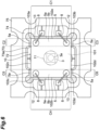
- a light detection device 1A includes a wiring substrate 2, a light detector 3, a plurality of spacers 4, a plurality of adhesive members 5, and a Fabry-Perot interference filter 10.
- the Fabry-Perot interference filter 10 has a first mirror 31 and a second mirror 41 with variable distance therebetween.
- the light detection device 1A is a spectroscopic sensor capable of obtaining a spectral spectrum.
- the light detection device 1A if light is externally incident on a light transmission region 11 of the Fabry-Perot interference filter 10, light having a predetermined wavelength is selectively transmitted according to a distance between the first mirror 31 and the second mirror 41 in the light transmission region 11 and the light transmitted through the light transmission region 11 of the Fabry-Perot interference filter 10 is detected by the light detector 3.
- the light detector 3 and a temperature compensation element such as a thermistor are mounted on the wiring substrate 2.
- a substrate material of the wiring substrate silicon, ceramic, quartz, glass, plastic, or the like, for example can be used.
- the light detector 3 has a light reception unit 3a that receives the light transmitted through the light transmission region 11 of the Fabry-Perot interference filter 10.
- the light transmission region 11 and the light reception unit 3a face each other in a direction A in which the light transmits the light transmission region 11.
- an infrared detector can be used.
- the infrared detector a quantum-type sensor using InGaAs and a thermal-type sensor using a thermopile or a bolometer can be used.
- a silicon photodiode can be used as the light detector 3.
- one light reception unit 3a may be provided or a plurality of light reception units 3a may be provided in an array shape.
- the plurality of light detectors 3 may be mounted on the wiring substrate 2.
- the plurality of spacers 4 are fixed on the wiring substrate 2 by adhesive members (not illustrated in the drawings).
- the Fabry-Perot interference filter 10 is fixed on the plurality of spacers 4 by the adhesive members 5.
- the plurality of spacers 4 function as support members to support the Fabry-Perot interference filter 10 on the wiring substrate 2.
- the light detector 3 is disposed in a space formed between the wiring substrate 2 and the Fabry-Perot interference filter 10 by the plurality of spacers 4.
- silicon, ceramic, quartz, glass, and plastic or the like for example can be used.
- a material of each spacer 4 is preferably a material of which a thermal expansion coefficient is equal to a thermal expansion coefficient of the material of the Fabry-Perot interference filter 10.
- the wiring substrate 2 and the spacers 4 may be integrally formed.
- the Fabry-Perot interference filter 10 may be supported by one spacer 4, not the plurality of spacers 4.
- flexible resin materials for example, resin materials such as silicone resins, urethane resins, epoxy resins, acrylic resins, and hybrid resins, which may be conductive or non-conductive
- resin materials are preferably selected from materials of which Young's modulus is less than 1000 MPa and are more preferably selected from materials of which Young's modulus is less than 10 MPa.
- the resin materials are preferably selected from materials of which glass transition temperatures are out of use environment temperatures of the light detection device 1A.
- Young's modulus after curing becomes less than 10 MPa and a glass transition temperature becomes about -50 to -40°C lower than the use environment temperatures (for example, about 5 to 40°C).
- elastic modulus of the adhesive members 5 to adhere the Fabry-Perot interference filter 10 and the individual spacers 4 to each other is smaller than elastic modulus of the spacers 4.
- the elastic modulus of the adhesive members 5 to adhere the Fabry-Perot interference filter 10 and the individual spacers 4 to each other is smaller than elastic modulus of the adhesive members (not illustrated in the drawings) to adhere the wiring substrate 2 and the individual spacers 4 to each other.
- Young's modulus after curing becomes 100 MPa or more.
- the Young's modulus of the spacer 4 becomes 100 GPa or more when the spacer is made of silicon, becomes 100 GPa or more when the spacer is made of ceramic, becomes 10 GPa or more (generally, 70 to 80 GPa) when the spacer is made of glass, and becomes 0.1 GPa or more when the spacer is made of plastic.
- the elastic modulus is a generic term for the Young's modulus (longitudinal elastic modulus: a relation of tensile/compression stress and distortion), horizontal elastic modulus (a relation of shearing stress and distortion), and volume elastic modulus (a relation of a pressure and volumetric distortion under uniform compression). That is, the Young's modulus is a specific example of the elastic modulus.
- the light detection device 1A further includes a CAN package 6.
- the CAN package 6 accommodates the wiring substrate 2, the light detector 3, the temperature compensation element (not illustrated in the drawings), the plurality of spacers 4, the plurality of adhesive members 5, and the Fabry-Perot interference filter 10.
- the CAN package 6 has a stem 61 and a cap 62.
- An opening 62a is provided in the cap 62 and a plate-like light transmission member 63 is fixed on the opening 62a from the inner side.
- the light transmission region 11 and the opening 62a face each other in the direction A.
- a material of the light transmission member 63 a material (for example, glass, silicon, and germanium) corresponding to a measurement wavelength range of the light detection device 1A can be used.
- a light reflection prevention layer may be formed on at least one of a surface and a back surface of the light transmission member 63.
- a band-pass filter to transmit only light in the measurement wavelength range may be used as the light transmission member 63.
- the wiring substrate 2 is fixed on the stem 61.
- Each of an electrode pad provided in the wiring substrate 2, a terminal of the light detector 3, a terminal of the temperature compensation element, and terminals 12 and 13 of the Fabry-Perot interference filter 10 is electrically connected to each of a plurality of lead pins 9 penetrating the stem 61 by wires 8.
- an input/output of an electric signal with respect to each of the light detector 3, the temperature compensation element, and the Fabry-Perot interference filter 10 is enabled.
- the spacers 4 are disposed right below the terminals 12 and 13 of the Fabry-Perot interference filter 10, wire bonding can be surely performed.
- the light detection device 1A configured as described above, if light is incident on the light transmission region 11 of the Fabry-Perot interference filter 10 through the opening 62a and the light transmission member 63 from the outside, light having a predetermined wavelength is selectively transmitted according to the distance between the first mirror 31 and the second mirror 41 in the light transmission region 11.
- the light transmitted through the first mirror 31 and the second mirror 41 is incident on the light reception unit 3a of the light detector 3 and is detected by the light detector 3.
- the light transmitted through the first mirror 31 and the second mirror 41 is detected by the light detector 3 while a voltage applied to the Fabry-Perot interference filter 10 is changed (that is, while the distance between the first mirror 31 and the second mirror 41 is changed), so that a spectral spectrum can be obtained.
- the Fabry-Perot interference filter 10 includes a substrate 14. A reflection prevention layer 15, a first laminate 30, a sacrificial layer 16, and a second laminate 40 are laminated in this order on a surface 14a of a light incidence side of the substrate 14. An air gap S is formed between the first laminate 30 and the second laminate 40 by the sacrificial layer 16 of a frame shape. In the Fabry-Perot interference filter 10, the light is incident on the second laminate 40 from the side opposite to the substrate 14. In addition, light having a predetermined wavelength transmits the light transmission region 11 defined in a center portion of the Fabry-Perot interference filter 10.
- the substrate 14 is made of silicon, quartz, and glass, or the like, for example.
- the reflection prevention layer 15 and the sacrificial layer 16 are made of silicon oxide, for example.
- a thickness of the sacrificial layer 16 is preferably the integral multiple of 1/2 of a center transmission wavelength (that is, a center wavelength of a transmission wavelength range of the Fabry-Perot interference filter 10).
- a portion corresponding to the light transmission region 11 in the first laminate 30 functions as the first mirror 31.
- the first laminate 30 is configured by laminating a plurality of polysilicon layers and a plurality of silicon nitride layers alternately.
- An optical thickness of each of the polysilicon layer and the silicon nitride layer configuring the first mirror 31 is preferably the integral multiple of 1/4 of the center transmission wavelength.
- a silicon oxide layer may be used instead of the silicon nitride layer.
- a portion corresponding to the light transmission region 11 in the second laminate 40 functions as the second mirror 41 facing the first mirror 31 with the air gap S therebetween.
- the second laminate 40 is configured by laminating a plurality of polysilicon layers and a plurality of silicon nitride layers alternately.
- An optical thickness of each of the polysilicon layer and the silicon nitride layer configuring the second mirror 41 is preferably the integral multiple of 1/4 of the center transmission wavelength.
- a silicon oxide layer may be used instead of the silicon nitride layer.
- a plurality of through-holes 40b extending from a surface 40a of the second laminate 40 to the air gap S are provided to be distributed uniformly in a portion corresponding to the air gap S in the second laminate 40.
- the plurality of through-holes 40b are formed not to substantially affect a function of the second mirror 41.
- An inner diameter of each through-hole 40b is 100 nm to 5 ⁇ m.
- an opening area of the plurality of through-holes 40b occupies 0.01 to 10% of an area of the second mirror 41.
- the first mirror 31 and the second mirror 41 are supported on the substrate 14.
- the first mirror 31 is disposed on a light incidence side of the substrate 14.
- the second mirror 41 is disposed on a light incidence side of the first mirror 31 with the air gap S therebetween.
- a first electrode 17 is formed to surround the light transmission region 11.
- a second electrode 18 is formed to include the light transmission region 11.
- the first electrode 17 and the second electrode 18 are formed by doping impurities into the polysilicon layer and decreasing resistance.
- a size of the second electrode 18 is preferably a size including an entire region of the light transmission region 11. However, the size of the second electrode 18 may be nearly equal to a size of the light transmission region 11.
- a third electrode 19 is formed in the second mirror 41.
- the third electrode 19 faces the first electrode 17 and the second electrode 18 with the air gap S therebetween, in the direction A.
- the third electrode 19 is formed by doping the impurities into the polysilicon layer and decreasing resistance.
- the second electrode 18 is located at the side opposite to the third electrode 19 with respect to the first electrode 17, in the direction A. That is, the first electrode 17 and the second electrode 18 are not disposed on the same plane in the first mirror 31. The second electrode 18 is farther from the third electrode 19 than the first electrode 17.
- the terminals 12 apply a voltage to the Fabry-Perot interference filter 10.
- the pair of terminals 12 is provided to face each other with the light transmission region 11 therebetween.
- Each terminal 12 is disposed in the through-hole extending from the surface 40a of the second laminate 40 to the first laminate 30.
- Each terminal 12 is electrically connected to the first electrode 17 via a wiring line 21.
- the terminals 13 apply a voltage to the Fabry-Perot interference filter 10.
- the pair of terminals 13 is provided to face each other with the light transmission region 11 therebetween.
- a facing direction of the pair of terminals 12 and a facing direction of the pair of terminals 13 are orthogonal to each other.
- Each terminal 13 is electrically connected to the third electrode 19 via a wiring line 22.
- the third electrode 19 is electrically connected to the second electrode 18 via a wiring line 23.
- Trenches 26 and 27 are provided in the surface 30a of the first laminate 30.
- the trench 26 extends annularly to surround the wiring line 23 extending along the direction A from the terminal 13.
- the trench 26 electrically insulates the first electrode 17 and the wiring line 23 from each other.
- the trench 27 extends annularly along an inner edge of the first electrode 17.
- the trench 27 electrically insulates the first electrode 17 and an inner region of the first electrode 17 from each other.
- a region in each of the trenches 26 and 27 may be an insulating material and may be an air gap.
- a trench 28 is provided in the surface 40a of the second laminate 40.
- the trench 28 extends annularly to surround the terminal 12.
- a bottom surface of the trench 28 reaches the sacrificial layer 16.
- the trench 28 electrically insulates the terminal 12 and the third electrode 19 from each other.
- a region in the trench 28 may be an insulating material and may be an air gap.
- a reflection prevention layer 51, a third laminate 52, an intermediate layer 53, and a fourth laminate 54 are laminated in this order on a surface 14b of a light emission side of the substrate 14.
- the reflection prevention layer 51 and the intermediate layer 53 have the same configurations as the configurations of the reflection prevention layer 15 and the sacrificial layer 16.
- the third laminate 52 and the fourth laminate 54 have lamination structures symmetrical to lamination structures of the first laminate 30 and the second laminate 40, on the basis of the substrate 14.
- a laminate 50 is configured by the reflection prevention layer 5 1, the third laminate 52, the intermediate layer 53, and the fourth laminate 54.
- the laminate 50 is disposed on the light emission side of the substrate 14 and has a function of suppressing a warp of the substrate 14.
- a columnar opening 50a is provided to include the light transmission region 11.
- the opening 50a is opened to the light emission side and a bottom surface of the opening 50a reaches the reflection prevention layer 51.
- a light shielding layer 29a is formed on a surface 50b of the light emission side of the laminate 50.
- the light shielding layer 29a is made of aluminum.
- a protection layer 29b is formed on a surface of the light shielding layer 29a and an inner surface of the opening 50a.
- the protection layer 29b is made of aluminum oxide, for example.
- a thickness of the protection layer 29b is set to 1 to 100 nm (preferably, about 30 nm), so that an optical influence by the protection layer 29b can be ignored.
- the second mirror 41 is driven to be attracted to the side of the first mirror 31 fixed on the substrate 14.
- the wavelength of the light transmitting the Fabry-Perot interference filter 10 depends on the distance between the first mirror 31 and the second mirror 41 in the light transmission region 11. Therefore, the wavelength of the transmitting light can be appropriately selected by adjusting the voltage applied between the first electrode 17 and the third electrode 19.
- the second electrode 18 has the same potential as the potential of the third electrode 19 electrically connected to the second electrode 18. Therefore, the second electrode 18 functions as a compensation electrode to maintain the first mirror 31 and the second mirror 41 flat in the light transmission region 11.
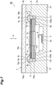
- FIGS. 3 and 4 A configuration of the adhesive members 5 will be described in detail with reference to FIGS. 3 and 4 .
- the wire 8 and the stem 61 are omitted and in FIG 4 , the wiring substrate 2, the wire 8, and the stem 61 are omitted.
- the Fabry-Perot interference filter 10 is supported by the pair of spacers 4A and 4B.
- a portion outside the light transmission region 11, which is a portion along a lateral surface 102a of the Fabry-Perot interference filter 10 is placed on a placement surface 4a of one spacer 4A.
- a portion outside the light transmission region 11, which is a portion along a lateral surface 102b of the Fabry-Perot interference filter 10 is placed on a placement surface 4a of the other spacer 4B.
- the Fabry-Perot interference filter 10 has a rectangular lateral surface 102 when viewed from the direction A.
- the lateral surface (first or second lateral surface) 102a and the lateral surface (first or third lateral surface) 102b face each other with the light transmission region 11 therebetween.
- the lateral surface 102a is located on the placement surface 4a of the spacer 4A, such that a part of the placement surface 4a of the spacer 4A is disposed outside the lateral surface 102a (outside the lateral surface 102 when viewed from the direction A).
- a corner portion C1 space in an end portion where the lateral surface 102a and a part of the placement surface 4a of the spacer 4A cross each other
- a portion (exposed portion on which the Fabry-Perot interference filter 10 is not placed) outside the lateral surface 102a in the placement surface 4a of the spacer 4A.
- One end portion of the side of an angular portion 103a of the lateral surface (fifth lateral surface) 102c forming the angular portion 103a with the lateral surface (fourth lateral surface) 102a in the lateral surface 102 is located on the placement surface 4a of the spacer 4A, such that a part of the placement surface 4a of the spacer 4A is disposed outside the lateral surface 102c.
- a corner portion C2 (space in an end portion where the lateral surface 102c and the part of the placement surface 4a of the spacer 4A cross each other) is formed by one end portion of the lateral surface 102c and a portion (exposed portion on which the Fabry-Perot interference filter 10 is not placed) outside one end portion of the lateral surface 102c in the placement surface 4a of the spacer 4A.
- One end portion of the side of an angular portion 103b of the lateral surface (fifth lateral surface) 102d forming the angular portion 103b with the lateral surface (fourth lateral surface) 102a in the lateral surface 102 is located on the placement surface 4a of the spacer 4A, such that a part of the placement surface 4a of the spacer 4A is disposed outside the lateral surface 102d.
- a corner portion C3 (space in an end portion where the lateral surface 102d and the part of the placement surface 4a of the spacer 4A cross each other) is formed by one end portion of the lateral surface 102d and a portion (exposed portion on which the Fabry-Perot interference filter 10 is not placed) outside one end portion of the lateral surface 102d in the placement surface 4a of the spacer 4A.
- the lateral surface 102a, one end portion of the lateral surface 102c, and one end portion of the lateral surface 102d correspond to a part of an outer edge of the Fabry-Perot interference filter 10, when viewed from the direction A.
- the lateral surface 102b is located on the placement surface 4a of the spacer 4B, such that a part of the placement surface 4a of the spacer 4B is disposed outside the lateral surface 102b.
- a corner portion C4 space in an end portion where the lateral surface 102b and the part of the placement surface 4a of the spacer 4B cross each other is formed by the lateral surface 102b and a portion (exposed portion on which the Fabry-Perot interference filter 10 is not placed) outside the lateral surface 102b in the placement surface 4a of the spacer 4B.
- the other end portion of the side of an angular portion 103c of the lateral surface (fifth lateral surface) 102c forming the angular portion 103c with the lateral surface (fourth lateral surface) 102b in the lateral surface 102 is located on the placement surface 4a of the spacer 4B, such that the part of the placement surface 4a of the spacer 4B is disposed outside the lateral surface 102c.
- a corner portion C5 space in an end portion where the lateral surface 102c and the part of the placement surface 4a of the spacer 4B cross each other
- a portion is formed by the other end portion of the lateral surface 102c and a portion (exposed portion on which the Fabry-Perot interference filter 10 is not placed) outside the other end portion of the lateral surface 102c in the placement surface 4a of the spacer 4B.
- the other end portion of the side of an angular portion 103d of the lateral surface (fifth lateral surface) 102d forming the angular portion 103d with the lateral surface (fourth lateral surface) 102b in the lateral surface 102 is located on the placement surface 4a of the spacer 4B, such that the part of the placement surface 4a of the spacer 4B is disposed outside the lateral surface 102d.
- a corner portion C6 space in an end portion where the lateral surface 102d and the part of the placement surface 4a of the spacer 4B cross each other
- a corner portion C6 is formed by the other end portion of the lateral surface 102d and a portion (exposed portion on which the Fabry-Perot interference filter 10 is not placed) outside the other end portion of the lateral surface 102d in the placement surface 4a of the spacer 4B.
- the lateral surface 102b, the other end portion of the lateral surface 102c, and the other end portion of the lateral surface 102d correspond to a part of the outer edge of the Fabry-Perot interference filter 10, when viewed from the direction A.
- the adhesive members 5 are disposed in the individual corner portions C1, C2, and C3 and the adhesive members 5 disposed in the individual corner portions C1, C2, and C3 are continuous with each other. That is, the adhesive members 5 disposed on the placement surface 4a of the spacer 4A are continuous over the entire corner portion C1 and cover the individual angular portions 103a and 103b from the outside.
- the adhesive members 5 are disposed in the individual corner portions C4, C5, and C6 and the adhesive members 5 disposed in the individual corner portions C4, C5, and C6 are continuous with each other. That is, the adhesive members 5 disposed on the placement surface 4a of the spacer 4B are continuous over the entire corner portion C4 and cover the individual angular portions 103c and 103d from the outside.
- the adhesive member 5 disposed on the placement surface 4a of the spacer 4A includes a first portion 5a and a second portion 5b.
- the first portion 5a is a portion disposed along the individual corner portions C1, C2, and C3 and is continuous through the individual angular portions 103a and 103b.
- the second portion 5b is a portion disposed between the placement surface 4a of the spacer 4A and the bottom surface 101 of the Fabry-Perot interference filter 10.
- the first portion 5a contacts each of the lateral surface 102a and the placement surface 4a of the spacer 4A.
- the first portion 5a contacts each of one end portion of the lateral surface 102c and the placement surface 4a of the spacer 4A.
- the first portion 5a contacts each of one end portion of the lateral surface 102d and the placement surface 4a of the spacer 4A. That is, the adhesive member 5 disposed on the placement surface 4a of the spacer 4A contacts each of the lateral surface 102 and the placement surface 4a of the spacer 4A.
- the adhesive member 5 disposed on the placement surface 4a of the spacer 4B includes a first portion 5a and a second portion 5b.
- the first portion 5a is a portion disposed along the individual corner portions C4, C5, and C6 and is continuous through the individual angular portions 103c and 103d.
- the second portion 5b is a portion disposed between the placement surface 4a of the spacer 4B and the bottom surface 101 of the Fabry-Perot interference filter 10.
- the first portion 5a contacts each of the lateral surface 102b and the placement surface 4a of the spacer 4B.
- the first portion 5a contacts each of the other end portion of the lateral surface 102c and the placement surface 4a of the spacer 4B.
- the first portion 5a contacts each of the other end portion of the lateral surface 102d and the placement surface 4a of the spacer 4B. That is, the adhesive member 5 disposed on the placement surface 4a of the spacer 4B contacts each of the lateral surface 102 and the placement surface 4a of the spacer 4B.
- a highest edge portion 5c of the first portion 5a reaches the lateral surface of the substrate 14 of the Fabry-Perot interference filter 10. That is, the adhesive member 5 disposed on the placement surface 4a of the spacer 4A contacts the substrate 14 in the lateral surface 102.
- a highest edge portion 5c of the first portion 5a reaches the lateral surface of the substrate 14 of the Fabry-Perot interference filter 10. That is, the adhesive member 5 disposed on the placement surface 4a of the spacer 4B contacts the substrate 14 in the lateral surface 102.
- each of a height H of the first portion 5a in a direction vertical to the placement surface 4a of each of the spacers 4A and 4B and a width W of the first portion 5a in a direction vertical to the lateral surface 102 of the Fabry-Perot interference filter 10 is 10 to 1000 ⁇ m.
- a thickness of the Fabry-Perot interference filter 10 is 100 to 1000 ⁇ m.
- a width (width in the direction vertical to the lateral surface 102) of a portion of the placement surface 4a that protrudes to the outside of the lateral surface 102 is 10 to 1000 ⁇ m.
- the height H of the first portion 5a is preferably equal to or more than 1/10 of the thickness of the Fabry-Perot interference filter 10 and less than the thickness of the Fabry-Perot interference filter 10.
- a distance between the bottom surface 101 and the surface 14b of the light emission side of the substrate 14 is 0.1 to 10 ⁇ m. For this reason, if the height H of the first portion 5a is set to 10 ⁇ m or more, the highest edge portion 5c of the first portion 5a can be caused to reach the lateral surface of the substrate 14 of the Fabry-Perot interference filter 10.
- a value (corresponding to the height of the edge portion 5c from the bottom surface 101 of the Fabry-Perot interference filter 10) obtained by subtracting the thickness of the second portion 5b in the direction vertical to the placement surface 4a in the adhesive member 5 from the height H of the first portion 5a in the direction vertical to the placement surface 4a is larger than the thickness of the second portion 5b in the direction vertical to the placement surface 4a.
- the adhesive members 5 having the elastic modulus smaller than the elastic modulus of the individual spacers 4A and 4B are disposed in the corner portions C1, C2, C3, C4, C5, and C6 and contact each of the lateral surface 102 of the Fabry-Perot interference filter and the parts of the placement surfaces 4a of the individual spacers 4A and 4B.
- the stress generated in the Fabry-Perot interference filter 10 due to the difference of the thermal expansion coefficients between the Fabry-Perot interference filter 10 and other members (the wiring substrate 2, the stem 61, and the cap 62 as well as the individual spacers 4A and 4B) configuring the light detection device 1A can be sufficiently absorbed into the adhesive members 5, as compared with the case in which the adhesive members 5 are merely interposed between the bottom surface 101 of the Fabry-Perot interference filter 10 and the placement surfaces 4a of the individual spacers 4A and 4B, for example.
- the Fabry-Perot interference filter 10 can be held on the spacers 4A and 4B more firmly in a stable state, as compared with the case in which the adhesive members 5 are merely interposed between the bottom surface 101 of the Fabry-Perot interference filter 10 and the placement surfaces 4a of the individual spacers 4A and 4B, for example. Therefore, according to the light detection device 1A, a temperature characteristic of the transmission wavelength in the Fabry-Perot interference filter 10 can be sufficiently improved and a holding state of the Fabry-Perot interference filter 10 on the spacers 4A and 4B can be stabilized.
- the adhesive member 5 preferably has the elastic modulus smaller than the elastic modulus of other members (the Fabry-Perot interference filter 10, the wiring substrate 2, the stem 61, and the cap 62 as well as the individual spacers 4A and 4B) configuring the light detection device 1A.
- the second portions 5b are interposed between the placement surfaces 4a of the individual spacers 4A and 4B and the bottom surface 101 of the Fabry-Perot interference filter 10, so that the stress generated in the Fabry-Perot interference filter 10 due to the difference of the thermal expansion coefficients between the Fabry-Perot interference filter 10 and other members configuring the light detection device 1A is absorbed. As a result, the generation of the stress in the Fabry-Perot interference filter 10 is suppressed.
- the thermal stress (stress generated from various areas and directions) generated in the CAN package 6 can be sufficiently recovered (absorption amount of the thermal stress by the adhesive member 5 > generation amount of the thermal stress in the CAN package 6). Therefore, the temperature characteristic of the transmission wavelength in the Fabry-Perot interference filter 10 is improved.
- the Fabry-Perot interference filter 10 is held between the placement surfaces 4a of the individual spacers 4A and 4B and the bottom surface 101 of the Fabry-Perot interference filter 10 and from the outside of the lateral surface 102. Therefore, the holding state of the Fabry-Perot interference filter 10 on the spacers 4A and 4B is stabilized.
- the configuration of the adhesive member 5 in the light detection device 1A can realize both improvement of the temperature characteristic of the transmission wavelength in the Fabry-Perot interference filter 10 and stabilization of the holding state of the Fabry-Perot interference filter 10 on the spacers 4A and 4B.
- the value obtained by subtracting the thickness of the second portion 5b in the direction vertical to the placement surface 4a in the adhesive member 5 from the height H of the first portion 5a in the direction vertical to the placement surface 4a is larger than the thickness of the second portion 5b in the direction vertical to the placement surface 4a.
- the adhesive member 5 preferably contacts the portion of the placement surface 4a protruding to the outside of the lateral surface 102, over the entire width thereof.
- the adhesive members 5 disposed in the corner portions C1, C2, C3, C4, C5, and C6 contact the substrate 14 in the lateral surface 102 of the Fabry-Perot interference filter 10.
- the stress generated in the Fabry-Perot interference filter 10 due to the difference of the thermal expansion coefficients between the Fabry-Perot interference filter 10 and other members configuring the light detection device 1A can be sufficiently absorbed into the adhesive members 5.
- the substrate 14 supporting the first mirror 31 and the second mirror 41 is externally held by the adhesive member 5, the holding state of the Fabry-Perot interference filter 10 can be further stabilized.
- the adhesive member 5 is disposed in the corner portion C1 to be continuous over the entire corner portion C1 formed by the lateral surface 102a of the Fabry-Perot interference filter 10 and contacts the lateral surface 102a.
- the adhesive member 5 is disposed in the corner portion C4 to be continuous over the entire corner portion C4 formed by the lateral surface 102b of the Fabry-Perot interference filter 10 and contacts the lateral surface 102b.
- the stress generated in the Fabry-Perot interference filter 10 due to the difference of the thermal expansion coefficients between the Fabry-Perot interference filter 10 and other members configuring the light detection device 1A can be uniformly absorbed into the adhesive members 5, as compared with the case in which the plurality of adhesive members 5 are intermittently disposed in the individual corner portions C1 and C4 or the case in which the adhesive member 5 is disposed in only one place in the parts of the individual corner portions C1 and C4, for example.
- the adhesive member 5 is formed as follows. That is, an adhesive material including the silicone resin material is applied to the placement surface 4a of each of the spacers 4A and 4B at a uniform thickness, the Fabry-Perot interference filter 10 is placed thereon, and in this state, the adhesive material is thermally cured, for example.
- the thickness of the adhesive material existing between the placement surface 4a of each of the spacers 4A and 4B and the bottom surface 101 of the Fabry-Perot interference filter 10 becomes uniform by the weight of the Fabry-Perot interference filter 10.
- the adhesive material existing in the corner portions C1, C2, C3, C4, C5, and C6 creeps up the lateral surface 102 of the Fabry-Perot interference filter 10 and has the uniform height and width. In this way, the adhesive member 5 including the first portion 5a having the uniform height H and width W is formed.
- the adhesive material including the silicone resin material may be thermally cured, for example. Even in this case, when the adhesive material is applied along the corner portions C1, C2, C3, C4, C5, and C6, the adhesive material enters between the placement surface 4a of each of the spacers 4A and 4B and the bottom surface 101 of the Fabry-Perot interference filter 10 and the thickness of the adhesive material becomes uniform by the weight of the Fabry-Perot interference filter 10.
- the adhesive material existing in the corner portions C1, C2, C3, C4, C5, and C6 creeps up the lateral surface 102 of the Fabry-Perot interference filter 10 and has the uniform height and width.
- the adhesive material including the silicone resin material may be applied to only a region of the placement surface 4a of each of the spacers 4A and 4B where the bottom surface 101 of the Fabry-Perot interference filter 10 is placed, the Fabry-Perot interference filter 10 may be placed, the adhesive material may be thermally cured, for example, the adhesive material including the silicone resin material may be applied along the corner portions C1, C2, C3, C4, C5, and C6 at the uniform thickness, and the adhesive material may be thermally cured, for example.
- the thickness of the adhesive material existing between the placement surface 4a of each of the spacers 4A and 4B and the bottom surface 101 of the Fabry-Perot interference filter 10 becomes uniform by the weight of the Fabry-Perot interference filter 10.
- the adhesive material existing in the corner portions C1, C2, C3, C4, C5, and C6 has the uniform height and width in the lateral surface 102 of the Fabry-Perot interference filter 10.
- the adhesive member 5 is disposed in the corner portion C1 formed by the lateral surface 102a of the Fabry-Perot interference filter 10 and contacts the lateral surface 102a. Furthermore, the adhesive member 5 is disposed in the corner portion C4 formed by the lateral surface 102b of the Fabry-Perot interference filter 10 facing the lateral surface 102a with the light transmission region 11 therebetween and contacts the lateral surface 102b. As a result, the Fabry-Perot interference filter 10 can be held on the spacers 4A and 4B in a more stable state.
- the adhesive member 5 in the case in which a material (for example, the silicone resin material) having extremely small Young's modulus (Young's modulus of less than 10 MPa) is used as the material of the adhesive member 5, even if the adhesive member 5 is disposed in each of the corner portions C1 and C4 formed by the lateral surfaces 102a and 102b facing each other, respectively, the distortion is suppressed from being generated in the Fabry-Perot interference filter 10 by the thermal stress generated in the CAN package 6 and the thermal stress generated in the CAN package 6 is absorbed by the adhesive member 5.
- a material for example, the silicone resin material having extremely small Young's modulus (Young's modulus of less than 10 MPa)
- the adhesive members 5 disposed in the individual corner portions C1, C2, and C3 are continuous with each other and cover the individual angular portions 103a and 103b of the Fabry-Perot interference filter 10 from the outside.
- the adhesive members 5 disposed in the individual corner portions C4, C5, and C6 are continuous with each other and cover the individual angular portions 103c and 103d of the Fabry-Perot interference filter 10 from the outside.
- the stress can be sufficiently absorbed into the adhesive member 5.
- the adhesive member 5 is not provided on the entire bottom surface 101 of the Fabry-Perot interference filter 10 (in particular, because the adhesive member 5 is not provided in the light transmission region 11), the following effects are obtained. That is, because the light transmitted through the Fabry-Perot interference filter 10 does not transmit the adhesive member 5, it becomes unnecessary to select the adhesive member 5 having high light transmittance, and a degree of freedom in selecting the adhesive member 5 is improved.
- the light transmitting the Fabry-Perot interference filter 10 is not affected by the change in the optical characteristics (the refractive index and the transmittance) of the adhesive member 5 due to the change in the ambient temperature.
- the Fabry-Perot interference filter 10 is suppressed from being distorted or inclined due to the stress generated by the contraction of the adhesive member 5 at the time of curing and the expansion and contraction of the adhesive member 5 due to the change in the ambient temperature at the time of use.
- a light detection device 1B is different from the light detection device 1A in that the light detection device 1B is configured as a surface mount device (SMD).
- the light detection device 1B includes an SMD package 7 that accommodates a light detector 3, a temperature compensation element (not illustrated in the drawings), and a Fabry-Perot interference filter 10.
- the SMD package 7 has a first layer substrate 71, a second layer substrate 72, a third layer substrate 73, a fourth layer substrate 74, a fifth layer substrate 75, and a sixth layer substrate 76.
- the first layer substrate 71, the second layer substrate 72, the third layer substrate 73, the fourth layer substrate 74, the fifth layer substrate 75, and the sixth layer substrate 76 are laminated in this order.
- An opening is provided in a center portion of each of the second layer substrate 72, the third layer substrate 73, the fourth layer substrate 74, and the fifth layer substrate 75.
- the opening of the third layer substrate 73 includes the opening of the second layer substrate 72, when viewed from a direction A.
- the opening of the fourth layer substrate 74 includes the opening of the third layer substrate 73, when viewed from the direction A.
- the opening of the fifth layer substrate 75 includes the opening of the fourth layer substrate 74, when viewed from the direction A.
- the light detector 3 and the temperature compensation element (not illustrated in the drawings) are mounted on the exposed surface of the first layer substrate 71.
- a plurality of electrode pads 77 are provided on a back surface of the first layer substrate 71.
- Each terminal of the light detector 3 and each terminal of the temperature compensation element are electrically connected to the electrode pads 77 by wiring lines provided in the first layer substrate 71 or wires 8 and wiring lines provided in the individual substrates 71 and 72.
- the Fabry-Perot interference filter 10 is fixed on the exposed surface of the third layer substrate 73 by adhesive members 5. Heights of top surfaces of individual terminals 12 and 13 of the Fabry-Perot interference filter 10 are the same as a height of a top surface of the fourth layer substrate 74. Pads electrically connected to the electrode pads 77 are provided on the top surface of the fourth layer substrate 74 and the individual terminals 12 and 13 are connected to the pads on the top surface of the fourth layer substrate 74 by the wires 8. The individual terminals 12 and 13 of the Fabry-Perot interference filter 10 are electrically connected to the electrode pads 77 by the wires 8 and the wiring lines provided in the individual substrates 71, 72, 73, and 74.
- the third layer substrate 73 functions as a support member to support the Fabry-Perot interference filter 10 on the first layer substrate 71 and the second layer substrate 72.
- a thermal expansion coefficient of the material of the third layer substrate 73 is preferably the same as a thermal expansion coefficient of a material of the Fabry-Perot interference filter 10 to alleviate a difference of the thermal expansion coefficients between the Fabry-Perot interference filter 10 and the third layer substrate 73.
- flexible resin materials for example, resin materials such as silicone resins, urethane resins, epoxy resins, acrylic resins, and hybrid resins, which may be conductive or non-conductive
- resin materials are preferably selected from materials of which Young's modulus is less than 1000 MPa and are more preferably selected from materials of which Young's modulus is less than 10 MPa.
- the resin materials are preferably selected from materials of which glass transition temperatures are out of use environment temperatures of the light detection device 1B.
- Young's modulus after curing becomes less than 10 MPa and a glass transition temperature becomes about -50 to -40°C lower than the use environment temperatures (for example, about 5 to 40 °C).
- elastic modulus of the adhesive members 5 to adhere the Fabry-Perot interference filter 10 and the third layer substrate 73 to each other is smaller than elastic modulus of the third layer substrate 73.
- the elastic modulus of the adhesive members 5 to adhere the Fabry-Perot interference filter 10 and the third layer substrate 73 to each other is smaller than elastic modulus of adhesive members (not illustrated in the drawings) to adhere the first layer substrate 71, the second layer substrate 72, the third layer substrate 73, the fourth layer substrate 74, the fifth layer substrate 75, and the sixth layer substrate 76 to each other.
- Young's modulus after curing becomes 100 MPa or more.
- the sixth layer substrate 76 has a light transmission substrate 76a and a light shielding layer 76b.
- the light transmission substrate 76a is fixed on the fifth layer substrate 75 by an adhesive member (not illustrated in the drawings).
- a material of the light transmission substrate 76a a material (for example, glass, silicon, and germanium) corresponding to a measurement wavelength range of the light detection device 1B can be used.
- the light shielding layer 76b is formed on a surface of the light transmission substrate 76a.
- a light shielding material or a light absorption material for example, a metal such as aluminum, a metal oxide such as a chromium oxide, and a black resin.
- the light shielding layer 76b is provided with an opening 76c. A light transmission region 11 and the opening 76c face each other in the direction A.
- the light shielding layer 76b may be formed on a back surface of the light transmission substrate 76a.
- a light reflection prevention layer may be formed on at least one of the surface and the back surface of the light transmission substrate 76a.
- a band-pass filter transmitting only light in the measurement wavelength range may be used as the light transmission substrate 76a.
- the light detection device 1B configured as described above, if light is incident on the light transmission region 11 of the Fabry-Perot interference filter 10 through the opening 76c and the light transmission substrate 76a from the outside, light having a predetermined wavelength is selectively transmitted according to a distance between a first mirror 31 and a second mirror 41 in the light transmission region 11.
- the light transmitted through the first mirror 31 and the second mirror 41 is incident on a light reception unit 3a of the light detector 3 and is detected by the light detector 3.
- the light transmitted through the first mirror 31 and the second mirror 41 is detected by the light detector 3 while a voltage applied to the Fabry-Perot interference filter 10 is changed (that is, the distance between the first mirror 31 and the second mirror 41 is changed), so that a spectral spectrum can be obtained.
- FIG. 6 A configuration of the adhesive members 5 will be described in detail with reference to FIGS. 5 and 6 .
- the sixth layer substrate 76 is omitted.
- the Fabry-Perot interference filter 10 has the rectangular lateral surface 102 when viewed from the direction A.
- lateral surface (first or second lateral surface) 102a and lateral surface (first or third lateral surface) 102b face each other with the light transmission region 11 therebetween.
- the lateral surface 102a is located on the placement surface 73a, such that a part of the placement surface 73a is disposed outside the lateral surface 102a (outside the lateral surface 102 when viewed from the direction A). As a result, a corner portion C1 is formed by the lateral surface 102a and a portion (exposed portion on which the Fabry-Perot interference filter 10 is not placed) outside the lateral surface 102a in the placement surface 73a.
- One end portion of the side of an angular portion 103a of the lateral surface (fifth lateral surface) 102c forming the angular portion 103a with the lateral surface (fourth lateral surface) 102a in the lateral surface 102 is located on the placement surface 73a, such that a part of the placement surface 73a is disposed outside the lateral surface 102c.
- a corner portion C2 is formed by one end portion of the lateral surface 102c and a portion (exposed portion on which the Fabry-Perot interference filter 10 is not placed) outside one end portion of the lateral surface 102c in the placement surface 73a.
- One end portion of the side of an angular portion 103b of the lateral surface (fifth lateral surface) 102d forming the angular portion 103b with the lateral surface (fourth lateral surface) 102a in the lateral surface 102 is located on the placement surface 73a, such that a part of the placement surface 73a is disposed outside the lateral surface 102d.
- a corner portion C3 is formed by one end portion of the lateral surface 102d and a portion (exposed portion on which the Fabry-Perot interference filter 10 is not placed) outside one end portion of the lateral surface 102d in the placement surface 73a.
- the lateral surface 102a, one end portion of the lateral surface 102c, and one end portion of the lateral surface 102d correspond to a part of an outer edge of the Fabry-Perot interference filter 10, when viewed from the direction A.
- the lateral surface 102b is located on the placement surface 73a, such that a part of the placement surface 73a is disposed outside the lateral surface 102b.
- a corner portion C4 is formed by the lateral surface 102b and a portion (exposed portion on which the Fabry-Perot interference filter 10 is not placed) outside the lateral surface 102b in the placement surface 73a.
- the other end portion of the side of an angular portion 103c of the lateral surface (fifth lateral surface) 102c forming the angular portion 103c with the lateral surface (fourth lateral surface) 102b in the lateral surface 102 is located on the placement surface 73a, such that a part of the placement surface 73a is disposed outside the lateral surface 102c.
- a corner portion C5 is formed by the other end portion of the lateral surface 102c and a portion (exposed portion on which the Fabry-Perot interference filter 10 is not placed) outside the other end portion of the lateral surface 102c in the placement surface 73a.
- the other end portion of the side of an angular portion 103d of the lateral surface (fifth lateral surface) 102d forming the angular portion 103d with the lateral surface (fourth lateral surface) 102b in the lateral surface 102 is located on the placement surface 73a, such that a part of the placement surface 73a is disposed outside the lateral surface 102d.
- a corner portion C6 is formed by the other end portion of the lateral surface 102d and a portion (exposed portion on which the Fabry-Perot interference filter 10 is not placed) outside the other end portion of the lateral surface 102d in the placement surface 73a.
- the lateral surface 102b, the other end portion of the lateral surface 102c, and the other end portion of the lateral surface 102d correspond to a part of the outer edge of the Fabry-Perot interference filter 10, when viewed from the direction A.
- the adhesive members 5 are disposed in the individual corner portions C1, C2, and C3.
- the adhesive members 5 disposed in the individual corner portions C1, C2, and C3 are continuous with each other. That is, the adhesive members 5 disposed in the individual corner portions C1, C2, and C3 are continuous over the entire corner portion C1 and cover the individual angular portions 103a and 103b from the outside.
- the adhesive members 5 are disposed in the individual corner portions C4, C5, and C6.
- the adhesive members 5 disposed in the individual corner portions C4, C5, and C6 are continuous with each other. That is, the adhesive members 5 disposed in the individual corner portions C4, C5, and C6 are continuous over the entire corner portion C4 and cover the individual angular portions 103c and 103d from the outside.
- the adhesive member 5 disposed in the individual corner portions C1, C2, and C3 includes a first portion 5a and a second portion 5b.
- the first portion 5a is a portion disposed along the individual corner portions C1, C2, and C3 and is continuous through the individual angular portions 103a and 103b.
- the second portion 5b is a portion disposed between the placement surface 73a of the third layer substrate 73 and the bottom surface 101 of the Fabry-Perot interference filter 10.
- the first portion 5a contacts each of the lateral surface 102a, the placement surface 73a, and an inner surface 74a of the opening of the fourth layer substrate 74.
- the first portion 5a contacts each of one end portion of the lateral surface 102c, the placement surface 73a, and the inner surface 74a of the opening of the fourth layer substrate 74.
- the first portion 5a contacts each of one end portion of the lateral surface 102d, the placement surface 73a, and the inner surface 74a of the opening of the fourth layer substrate 74. That is, the adhesive member 5 disposed in the individual corner portions C1, C2, and C3 contacts each of the lateral surface 102, the placement surface 73a, and the inner surface 74a of the opening of the fourth layer substrate 74.
- the adhesive member 5 disposed in the individual corner portions C4, C5, and C6 includes a first portion 5a and a second portion 5b.
- the first portion 5a is a portion disposed along the individual corner portions C4, C5, and C6 and is continuous through the individual angular portions 103c and 103d.
- the second portion 5b is a portion disposed between the placement surface 73a of the third layer substrate 73 and the bottom surface 101 of the Fabry-Perot interference filter 10.
- the first portion 5a contacts each of the lateral surface 102b, the placement surface 73a, and the inner surface 74a of the opening of the fourth layer substrate 74.
- the first portion 5a contacts each of the other end portion of the lateral surface 102c, the placement surface 73a, and the inner surface 74a of the opening of the fourth layer substrate 74.
- the first portion 5a contacts each of the other end portion of the lateral surface 102d, the placement surface 73a, and the inner surface 74a of the opening of the fourth layer substrate 74. That is, the adhesive member 5 disposed in the individual corner portions C4, C5, and C6 contacts each of the lateral surface 102, the placement surface 73a, and the inner surface 74a of the opening of the fourth layer substrate 74.
- a highest edge portion 5c of the first portion 5a at the side of the lateral surface 102 reaches a lateral surface of a substrate 14 of the Fabry-Perot interference filter 10. That is, the adhesive member 5 disposed in the individual corner portions C1, C2, and C3 contacts the substrate 14 in the lateral surface 102.
- a highest edge portion 5c of the first portion 5a at the side of the lateral surface 102 reaches the lateral surface of the substrate 14 of the Fabry-Perot interference filter 10. That is, the adhesive member 5 disposed in the individual corner portions C4, C5, and C6 contacts the substrate 14 in the lateral surface 102.
- a height of the edge portion 5c is smaller than heights of the Fabry-Perot interference filter 10 and the fourth layer substrate 74.
- a value (corresponding to the height of the edge portion 5c from the bottom surface 101 of the Fabry-Perot interference filter 10) obtained by subtracting the thickness of the second portion 5b in a direction vertical to the placement surface 73a in the adhesive member 5 from the height H of the first portion 5a in the direction vertical to the placement surface 73a is larger than the thickness of the second portion 5b in the direction vertical to the placement surface 73a.
- the adhesive members 5 having the elastic modulus smaller than the elastic modulus of the third layer substrate 73 are disposed in the corner portions C1, C2, C3, C4, C5, and C6 and contact each of the lateral surface 102 of the Fabry-Perot interference filter and the part of the placement surface 73a of the third layer substrate 73.
- the Fabry-Perot interference filter 10 can be held on the third layer substrate 73 more firmly in a stable state, as compared with the case in which the adhesive members 5 are merely interposed between the bottom surface 101 of the Fabry-Perot interference filter 10 and the placement surface 73a of the third layer substrate 73, for example. Therefore, according to the light detection device 1B, a temperature characteristic of the transmission wavelength in the Fabry-Perot interference filter 10 can be sufficiently improved and a holding state of the Fabry-Perot interference filter 10 on the third layer substrate 73 can be stabilized.
- the adhesive member 5 preferably has the elastic modulus smaller than the elastic modulus of other members (the Fabry-Perot interference filter 10, the first layer substrate 71, the second layer substrate 72, the fourth layer substrate 74, the fifth layer substrate 75, and the sixth layer substrate 76 as well as the third layer substrate 73) configuring the light detection device 1B.
- the Fabry-Perot interference filter 10 the first layer substrate 71, the second layer substrate 72, the fourth layer substrate 74, the fifth layer substrate 75, and the sixth layer substrate 76 as well as the third layer substrate 73
- the value obtained by subtracting the thickness of the second portion 5b in the direction vertical to the placement surface 73a in the adhesive member 5 from the height H of the first portion 5a in the direction vertical to the placement surface 73a is larger than the thickness of the second portion 5b in the direction vertical to the placement surface 73a.
- the adhesive member 5 preferably contacts a portion of the placement surface 73a protruding to the outside of the lateral surface 102, over the entire width thereof.
- the adhesive members 5 disposed in the corner portions C1, C2, C3, C4, C5, and C6 contact the substrate 14 in the lateral surface 102 of the Fabry-Perot interference filter 10.
- the stress generated in the Fabry-Perot interference filter 10 due to the difference of the thermal expansion coefficients between the Fabry-Perot interference filter 10 and other members configuring the light detection device 1B can be sufficiently absorbed into the adhesive members 5.
- the substrate 14 supporting the first mirror 31 and the second mirror 41 is externally held by the adhesive member 5, the holding state of the Fabry-Perot interference filter 10 can be further stabilized.
- the adhesive member 5 is disposed in the corner portion C1 to be continuous over the entire corner portion C1 formed by the lateral surface 102a of the Fabry-Perot interference filter 10 and contacts the lateral surface 102a.
- the adhesive member 5 is disposed in the corner portion C4 to be continuous over the entire corner portion C4 formed by the lateral surface 102b of the Fabry-Perot interference filter 10 and contacts the lateral surface 102b.
- the stress generated in the Fabry-Perot interference filter 10 due to the difference of the thermal expansion coefficients between the Fabry-Perot interference filter 10 and other members configuring the light detection device 1B can be uniformly absorbed into the adhesive members 5, as compared with the case in which the plurality of adhesive members 5 are intermittently disposed in the individual corner portions C1 and C4 or the case in which the adhesive member 5 is disposed in only one place in the parts of the individual corner portions C1 and C4, for example.
- the adhesive member 5 is disposed in the corner portion C1 formed by the lateral surface 102a of the Fabry-Perot interference filter 10 and contacts the lateral surface 102a. Furthermore, the adhesive member 5 is disposed in the corner portion C4 formed by the lateral surface 102b of the Fabry-Perot interference filter 10 facing the lateral surface 102a with the light transmission region 11 therebetween and contacts the lateral surface 102b. As a result, the Fabry-Perot interference filter 10 can be held on the third layer substrate 73 in a more stable state.
- the adhesive members 5 disposed in the individual corner portions C1, C2, and C3 are continuous with each other and cover the individual angular portions 103a and 103b of the Fabry-Perot interference filter 10 from the outside.
- the adhesive members 5 disposed in the individual corner portions C4, C5, and C6 are continuous with each other and cover the individual angular portions 103c and 103d of the Fabry-Perot interference filter 10 from the outside.
- the stress can be sufficiently absorbed into the adhesive member 5.
- the adhesive member 5 is not provided on the entire bottom surface 101 of the Fabry-Perot interference filter 10 (particularly, because the adhesive member 5 is not provided in the light transmission region 11), the following effects are obtained. That is, because the light transmitted through the Fabry-Perot interference filter 10 does not transmit the adhesive member 5, it becomes unnecessary to select the adhesive member 5 having high light transmittance and a degree of freedom in selecting the adhesive member 5 is improved.
- the light transmitting the Fabry-Perot interference filter 10 is not affected by the change in the optical characteristics (the refractive index and the transmittance) of the adhesive member 5 due to the change in the ambient temperature.
- the Fabry-Perot interference filter 10 is suppressed from being distorted or inclined due to the stress generated by the contraction of the adhesive member 5 at the time of curing and the expansion and contraction of the adhesive member 5 due to the change in the ambient temperature at the time of use.
- the light detection device 1B horizontally long spaces (spaces where a width in a direction vertical to the direction A is larger than a width in a direction parallel to the direction A) are provided at both sides of the Fabry-Perot interference filter in the direction A.
- outer edges of the spaces provided at both sides of the Fabry-Perot interference filter in the direction A when viewed from the direction A are defined by an inner edge of the SMD package 7.
- the space provided at the light incidence side of the Fabry-Perot interference filter 10 is larger than the space provided at the light emission side of the Fabry-Perot interference filter 10 in the widths in the direction vertical to the direction A.
- the space provided at the light emission side of the Fabry-Perot interference filter 10 is larger than the space provided at the light incidence side of the Fabry-Perot interference filter 10 in the widths in the direction parallel to the direction A.
- the Fabry-Perot interference filter 10 is electrically connected to the plurality of electrode pads 77 provided on the bottom surface of the SMD package 7 via wiring lines provided in the SMD package 7.
- the light detection device 1B can be miniaturized.
- a distance between the opening 76c of the sixth layer substrate 76 and the Fabry-Perot interference filter 10 and a distance between the Fabry-Perot interference filter 10 and the light detector 3 can be decreased, as compared with the case in which vertically long spaces are provided. Therefore, even if light is incident from the opening 76c somewhat obliquely, the incidence light can be caused to transmit the light transmission region 11 of the Fabry-Perot interference filter 10 and the transmission light can be caused to be incident on the light reception unit 3a of the light detector 3.
- a volume of the SMD package 7 can be decreased by decreasing a height of a member configuring the SMD package 7, as compared with the case in which the vertically long spaces are provided. Therefore, the stress can be suppressed from being generated due to a difference of thermal expansion coefficients between the Fabry-Perot interference filter 10 and the SMD package 7.
- the adhesive member 5 includes the second portion 5b disposed between the placement surface 4a of the spacer 4A and the bottom surface 101 of the Fabry-Perot interference filter 10. However, if the adhesive member 5 includes the first portion 5a, the adhesive member 5 may not include the second portion 5b. Likewise, in the example, the adhesive member 5 includes the second portion 5b disposed between the placement surface 73a of the third layer substrate 73 and the bottom surface 101 of the Fabry-Perot interference filter 10. However, if the adhesive member 5 includes the first portion 5a, the adhesive member 5 may not include the second portion 5b.
- the adhesive member 5 includes the first portion 5a, the temperature characteristic of the transmission wavelength in the Fabry-Perot interference filter 10 can be sufficiently improved and the holding state of the Fabry-Perot interference filter 10 can be stabilized.
- a material and a shape of each configuration are not limited to the material and the shape described above and various materials and shapes can be adopted.
- the first layer substrate 71, the second layer substrate 72, the third layer substrate 73, the fourth layer substrate 74, and the fifth layer substrate 75 are formed separately.
- the bottom surface 101 of the Fabry-Perot interference filter 10 may be placed on a placement surface 70a of a support object (support object) 70 corresponding to an object obtained by integrally forming the substrates.
- a shape variation for every SMD package 7 formed is small as compared with the case where the first layer substrate 71, the second layer substrate 72, the third layer substrate 73, the fourth layer substrate 74, and the fifth layer substrate 75 are overlapped and adhered to each other.
- the adhesive members to adhere the first layer substrate 71, the second layer substrate 72, the third layer substrate 73, the fourth layer substrate 74, the fifth layer substrate 75, and the sixth layer substrate 76 to each other are unnecessary, a change in the shape of the SMD package 7 caused by the expansion and contraction of the adhesive member due to the change in the ambient temperature is suppressed.
- the adhesive member 5 between the Fabry-Perot interference filter 10 and the SMD package 7 can be suppressed from being deteriorated due to an influence of the moisture. Therefore, in this case, the SMD package 7 with a more stable shape can be obtained.
- the edge portion 5c of the adhesive member 5 reaches the lateral surface of the substrate 14 of the Fabry-Perot interference filter 10.
- the edge portion 5c of the adhesive member 5 does not reach the lateral surface of the substrate 14 and may reach the lateral surface of the laminate 50 of the Fabry-Perot interference filter 10. That is, the adhesive member 5 does not contact the lateral surface of the substrate 14 and may contact the lateral surface of the laminate 50.
- a light detection device capable of sufficiently improving a temperature characteristic of a transmission wavelength in a Fabry-Perot interference filter and stabilizing a holding state of the Fabry-Perot interference filter on a support member can be provided.
- 1A, 1B Optical detection device, 3: Light detector, 4, 4A, 4B: Spacer (support member), 4a: Placement surface, 5: Adhesive member, 5a: First portion, 5b: Second portion, 10: Fabry-Perot interference filter, 11: Light transmission region, 14: Substrate, 31: First mirror, 41: Second mirror, 70: Support object (support member), 70a: Placement surface, 73: Third layer substrate (support member), 73a: Placement surface, 101: Bottom surface, 102: Lateral surface, 102a: Lateral surface (first lateral surface, second lateral surface, fourth lateral surface), 102b: Lateral surface (first lateral surface, third lateral surface, fourth lateral surface), 102c, 102d: Lateral surface (fifth lateral surface), C1, C2, C3, C4, C5, C6: Corner portion.
Description
- The present invention relates to a light detection device including a Fabry-Perot interference filter that has a first mirror and a second mirror with variable distance therebetween.
- An optical module including an interference filter that has a first reflection film and a second reflection film with variable distance therebetween, a substrate that supports the interference filter, and an adhesive layer that is interposed between the interference filter and the substrate is described in Patent Literature 1. In the optical module described in Patent Literature 1, a gel-like resin is used in the adhesive layer to alleviate stress generated in the interference filter due to a difference of thermal expansion coefficients between the interference filter and the substrate.
US 2015/092274 A1 discloses an optical filter device including a wavelength variable interference filter stored in a housing and a bonding member that fixes a movable substrate to the housing.
US 2012/0212824 A1 relates to a colorimetry sensor including an interference filter which is fixed to a transparent substrate through an adhesive layer made of gel-like resin.
WO 01/22128 A1 - Patent Literature 1:
Japanese Unexamined Patent Publication No. 2012-173347 - However, when the Fabry-Perot interference filter that has the first mirror and the second mirror with the variable distance therebetween and a support member are fixed, it is necessary to control a distance between the first mirror and the second mirror with high precision. For this reason, if the adhesive layer made of the gel-like resin between is merely interposed between the Fabry-Perot interference filter and the support member, a variation in the stress generated in the Fabry-Perot interference filter due to a change in use environment temperatures cannot be sufficiently suppressed. As a result, a temperature characteristic of a transmission wavelength in the Fabry-Perot interference filter (a temperature characteristic for a wavelength of light transmitted by the Fabry-Perot interference filter) may not be sufficiently improved. If the adhesive layer made of the gel-like resin is used to fix the Fabry-Perot interference filter and the support member, a holding state of the Fabry-Perot interference filter on the support member may become unstable.
- Accordingly, an object of the present invention is to provide a light detection device capable of sufficiently improving a temperature characteristic of a transmission wavelength in a Fabry-Perot interference filter and stabilizing a holding state of the Fabry-Perot interference filter on a support member.
- A light detection device of an aspect of the present invention includes: a Fabry-Perot interference filter that has a first mirror and a second mirror with variable distance therebetween and is provided with a light transmission region to transmit light according to a distance between the first mirror and the second mirror; a light detector that detects the light transmitted through the light transmission region; a support member that has a placement surface on which a portion outside the light transmission region in a bottom surface of the Fabry-Perot interference filter is placed; and an adhesive member that adheres the Fabry-Perot interference filter and the support member to each other, wherein elastic modulus of the adhesive member is smaller than elastic modulus of the support member, at least a part of a lateral surface of the Fabry-Perot interference filter is located on the placement surface such that a part of the placement surface is disposed outside the lateral surface, and the adhesive member is disposed in a corner portion formed by the lateral surface and the part of the placement surface and contacts each of the lateral surface and the part of the placement surface.
- In the light detection device, the adhesive member having the elastic modulus smaller than the elastic modulus of the support member is disposed in the corner portion formed by the lateral surface of the Fabry-Perot interference filter and the part of the placement surface of the support member and contacts each of the lateral surface of the Fabry-Perot interference filter and the part of the placement surface of the support member. As a result, stress generated in the Fabry-Perot interference filter due to a difference of thermal expansion coefficients between the Fabry-Perot interference filter and the support member can be sufficiently absorbed into the adhesive member, as compared with the case in which the adhesive member is merely interposed between the bottom surface of the Fabry-Perot interference filter and the placement surface of the support member, for example. In addition, the Fabry-Perot interference filter can be held on the support member more firmly in a stable state, as compared with the case in which the adhesive member is merely interposed between the bottom surface of the Fabry-Perot interference filter and the placement surface of the support member, for example. Therefore, according to the light detection device, a temperature characteristic of a transmission wavelength in the Fabry-Perot interference filter can be sufficiently improved and a holding state of the Fabry-Perot interference filter on the support member can be stabilized.
- In the light detection device of an aspect of the present invention, the adhesive member may include a first portion disposed in the corner portion and a second portion disposed between the placement surface and the bottom surface, and a value obtained by subtracting a thickness of the second portion in a direction vertical to the placement surface from a height of the first portion in the direction vertical to the placement surface may be larger than the thickness of the second portion. As a result, the stress generated in the Fabry-Perot interference filter due to the difference of the thermal expansion coefficients between the Fabry-Perot interference filter and the support member can be sufficiently absorbed into the adhesive member.
- In the light detection device of an aspect of the present invention, the Fabry-Perot interference filter may further have a substrate supporting the first mirror and the second mirror, and the adhesive member disposed in the corner portion may contact the substrate in the lateral surface. As a result, the stress generated in the Fabry-Perot interference filter due to the difference of the thermal expansion coefficients between the Fabry-Perot interference filter and the support member can be sufficiently absorbed into the adhesive member. In addition, because the substrate supporting the first mirror and the second mirror is externally held by the adhesive member, the holding state of the Fabry-Perot interference filter can be further stabilized.
- In the light detection device of an aspect of the present invention, the lateral surface may include a first lateral surface, and the adhesive member may be disposed in the corner portion formed by the first lateral surface to be continuous over the entire corner portion formed by the first lateral surface and may contact the first lateral surface. As a result, the stress generated in the Fabry-Perot interference filter due to the difference of the thermal expansion coefficients between the Fabry-Perot interference filter and the support member can be uniformly absorbed into the adhesive member, as compared with the case in which a plurality of adhesive members are intermittently disposed in the corner portion formed by the first lateral surface, for example.
- In the light detection device of an aspect of the present invention, the lateral surface may include a second lateral surface and a third lateral surface facing each other with the light transmission region therebetween, and the adhesive member may be disposed in each of the corner portion formed by the second lateral surface and the corner portion formed by the third lateral surface and may contact each of the second lateral surface and the third lateral surface. As a result, the Fabry-Perot interference filter can be held on the support member in a more stable state.
- In the light detection device of an aspect of the present invention, the lateral surface may include a fourth lateral surface and a fifth lateral surface forming an angular portion, and the adhesive member may be disposed in each of the corner portion formed by the fourth lateral surface and the corner portion formed by the fifth lateral surface and may contact each of the fourth lateral surface and the fifth lateral surface. As a result, in the angular portion on which the stress generated in the Fabry-Perot interference filter due to the difference of the thermal expansion coefficients between the Fabry-Perot interference filter and the support member easily concentrates, the stress can be sufficiently absorbed into the adhesive member.
- In the light detection device of an aspect of the present invention, the adhesive member disposed in the corner portion formed by the fourth lateral surface and the adhesive member disposed in the corner portion formed by the fifth lateral surface may be continuous with each other. As a result, in the angular portion on which the stress generated in the Fabry-Perot interference filter due to the difference of the thermal expansion coefficients between the Fabry-Perot interference filter and the support member easily concentrates, the stress can be sufficiently absorbed into the adhesive member.
- According to the present invention, a light detection device capable of sufficiently improving a temperature characteristic of a transmission wavelength in a Fabry-Perot interference filter and stabilizing a holding state of the Fabry-Perot interference filter on a support member can be provided.
-
-
FIG 1 is a cross-sectional view of a light detection device according to a first embodiment. -
FIG. 2 is a cross-sectional view of a Fabry-Perot interference filter of the light detection device ofFIG. 1 . -
FIG. 3 is a plan view of a portion including the Fabry-Perot interference filter, spacers, and adhesive members in the light detection device ofFIG. 1 . -
FIG. 4 is a cross-sectional view of the portion including the Fabry-Perot interference filter, the spacers, and the adhesive members in the light detection device ofFIG. 1 . -
FIG. 5 is a cross-sectional view of a light detection device according to an example. -
FIG. 6 is a plan view of a portion including a Fabry-Perot interference filter, a third layer substrate, and adhesive members in the light detection device ofFIG. 5 . -
FIG. 7 is a cross-sectional view of a modification of the light detection device according to the example. - Hereinafter, a preferred embodiment of the present invention and an embodiment not claimed as the invention will be described in detail with reference to the drawings. In the individual drawings, the same or equivalent portions are denoted with the same reference numerals and overlapped portions are omitted.
- As illustrated in
FIG. 1 , alight detection device 1A includes awiring substrate 2, alight detector 3, a plurality ofspacers 4, a plurality ofadhesive members 5, and a Fabry-Perot interference filter 10. The Fabry-Perot interference filter 10 has afirst mirror 31 and asecond mirror 41 with variable distance therebetween. Thelight detection device 1A is a spectroscopic sensor capable of obtaining a spectral spectrum. That is, in thelight detection device 1A, if light is externally incident on alight transmission region 11 of the Fabry-Perot interference filter 10, light having a predetermined wavelength is selectively transmitted according to a distance between thefirst mirror 31 and thesecond mirror 41 in thelight transmission region 11 and the light transmitted through thelight transmission region 11 of the Fabry-Perot interference filter 10 is detected by thelight detector 3. - The
light detector 3 and a temperature compensation element (not illustrated in the drawings) such as a thermistor are mounted on thewiring substrate 2. As examples of a substrate material of thewiring substrate 2, silicon, ceramic, quartz, glass, plastic, or the like, for example can be used. Thelight detector 3 has alight reception unit 3a that receives the light transmitted through thelight transmission region 11 of the Fabry-Perot interference filter 10. Thelight transmission region 11 and thelight reception unit 3a face each other in a direction A in which the light transmits thelight transmission region 11. As an example of thelight detector 3, an infrared detector can be used. As examples of the infrared detector, a quantum-type sensor using InGaAs and a thermal-type sensor using a thermopile or a bolometer can be used. When light of individual wavelength regions such as an ultraviolet wavelength region, a visible wavelength region, and a near-infrared wavelength region is detected, a silicon photodiode can be used as thelight detector 3. In thelight detector 3, onelight reception unit 3a may be provided or a plurality oflight reception units 3a may be provided in an array shape. In addition, the plurality oflight detectors 3 may be mounted on thewiring substrate 2. - The plurality of
spacers 4 are fixed on thewiring substrate 2 by adhesive members (not illustrated in the drawings). The Fabry-Perot interference filter 10 is fixed on the plurality ofspacers 4 by theadhesive members 5. The plurality ofspacers 4 function as support members to support the Fabry-Perot interference filter 10 on thewiring substrate 2. Thelight detector 3 is disposed in a space formed between thewiring substrate 2 and the Fabry-Perot interference filter 10 by the plurality ofspacers 4. As examples of a material of eachspacer 4, silicon, ceramic, quartz, glass, and plastic or the like, for example can be used. Particularly, to alleviate a difference of thermal expansion coefficients between the Fabry-Perot interference filter 10 and eachspacer 4, a material of eachspacer 4 is preferably a material of which a thermal expansion coefficient is equal to a thermal expansion coefficient of the material of the Fabry-Perot interference filter 10. in addition, thewiring substrate 2 and thespacers 4 may be integrally formed. In addition, the Fabry-Perot interference filter 10 may be supported by onespacer 4, not the plurality ofspacers 4. - As materials of the
adhesive members 5 to adhere the Fabry-Perot interference filter 10 and theindividual spacers 4 to each other, flexible resin materials (for example, resin materials such as silicone resins, urethane resins, epoxy resins, acrylic resins, and hybrid resins, which may be conductive or non-conductive) can be used. The resin materials are preferably selected from materials of which Young's modulus is less than 1000 MPa and are more preferably selected from materials of which Young's modulus is less than 10 MPa. In addition, the resin materials are preferably selected from materials of which glass transition temperatures are out of use environment temperatures of thelight detection device 1A. For example, if an adhesive material including the silicone resin material is used as the material of theadhesive member 5, Young's modulus after curing becomes less than 10 MPa and a glass transition temperature becomes about -50 to -40°C lower than the use environment temperatures (for example, about 5 to 40°C). - Here, elastic modulus of the
adhesive members 5 to adhere the Fabry-Perot interference filter 10 and theindividual spacers 4 to each other is smaller than elastic modulus of thespacers 4. In addition, the elastic modulus of theadhesive members 5 to adhere the Fabry-Perot interference filter 10 and theindividual spacers 4 to each other is smaller than elastic modulus of the adhesive members (not illustrated in the drawings) to adhere thewiring substrate 2 and theindividual spacers 4 to each other. For example, if an adhesive material including the epoxy resin material is used as the material of the adhesive members to adhere thewiring substrate 2 and theindividual spacers 4 to each other, Young's modulus after curing becomes 100 MPa or more. In addition, the Young's modulus of thespacer 4 becomes 100 GPa or more when the spacer is made of silicon, becomes 100 GPa or more when the spacer is made of ceramic, becomes 10 GPa or more (generally, 70 to 80 GPa) when the spacer is made of glass, and becomes 0.1 GPa or more when the spacer is made of plastic. In addition, the elastic modulus is a generic term for the Young's modulus (longitudinal elastic modulus: a relation of tensile/compression stress and distortion), horizontal elastic modulus (a relation of shearing stress and distortion), and volume elastic modulus (a relation of a pressure and volumetric distortion under uniform compression). That is, the Young's modulus is a specific example of the elastic modulus. - The
light detection device 1A further includes aCAN package 6. TheCAN package 6 accommodates thewiring substrate 2, thelight detector 3, the temperature compensation element (not illustrated in the drawings), the plurality ofspacers 4, the plurality ofadhesive members 5, and the Fabry-Perot interference filter 10. TheCAN package 6 has astem 61 and acap 62. Anopening 62a is provided in thecap 62 and a plate-likelight transmission member 63 is fixed on theopening 62a from the inner side. Thelight transmission region 11 and theopening 62a face each other in the direction A. As a material of thelight transmission member 63, a material (for example, glass, silicon, and germanium) corresponding to a measurement wavelength range of thelight detection device 1A can be used. In addition, a light reflection prevention layer may be formed on at least one of a surface and a back surface of thelight transmission member 63. In addition, a band-pass filter to transmit only light in the measurement wavelength range may be used as thelight transmission member 63. - The
wiring substrate 2 is fixed on thestem 61. Each of an electrode pad provided in thewiring substrate 2, a terminal of thelight detector 3, a terminal of the temperature compensation element, andterminals Perot interference filter 10 is electrically connected to each of a plurality oflead pins 9 penetrating thestem 61 bywires 8. As a result, an input/output of an electric signal with respect to each of thelight detector 3, the temperature compensation element, and the Fabry-Perot interference filter 10 is enabled. In thelight detection device 1A, because thespacers 4 are disposed right below theterminals Perot interference filter 10, wire bonding can be surely performed. - In the
light detection device 1A configured as described above, if light is incident on thelight transmission region 11 of the Fabry-Perot interference filter 10 through theopening 62a and thelight transmission member 63 from the outside, light having a predetermined wavelength is selectively transmitted according to the distance between thefirst mirror 31 and thesecond mirror 41 in thelight transmission region 11. The light transmitted through thefirst mirror 31 and thesecond mirror 41 is incident on thelight reception unit 3a of thelight detector 3 and is detected by thelight detector 3. In thelight detection device 1A, the light transmitted through thefirst mirror 31 and thesecond mirror 41 is detected by thelight detector 3 while a voltage applied to the Fabry-Perot interference filter 10 is changed (that is, while the distance between thefirst mirror 31 and thesecond mirror 41 is changed), so that a spectral spectrum can be obtained. - As illustrated in
FIG 2 , the Fabry-Perot interference filter 10 includes asubstrate 14. Areflection prevention layer 15, afirst laminate 30, asacrificial layer 16, and asecond laminate 40 are laminated in this order on asurface 14a of a light incidence side of thesubstrate 14. An air gap S is formed between thefirst laminate 30 and thesecond laminate 40 by thesacrificial layer 16 of a frame shape. In the Fabry-Perot interference filter 10, the light is incident on thesecond laminate 40 from the side opposite to thesubstrate 14. In addition, light having a predetermined wavelength transmits thelight transmission region 11 defined in a center portion of the Fabry-Perot interference filter 10. - In addition, the
substrate 14 is made of silicon, quartz, and glass, or the like, for example. When thesubstrate 14 is made of the silicon, thereflection prevention layer 15 and thesacrificial layer 16 are made of silicon oxide, for example. A thickness of thesacrificial layer 16 is preferably the integral multiple of 1/2 of a center transmission wavelength (that is, a center wavelength of a transmission wavelength range of the Fabry-Perot interference filter 10). - A portion corresponding to the
light transmission region 11 in thefirst laminate 30 functions as thefirst mirror 31. Thefirst laminate 30 is configured by laminating a plurality of polysilicon layers and a plurality of silicon nitride layers alternately. An optical thickness of each of the polysilicon layer and the silicon nitride layer configuring thefirst mirror 31 is preferably the integral multiple of 1/4 of the center transmission wavelength. In addition, instead of the silicon nitride layer, a silicon oxide layer may be used. - A portion corresponding to the
light transmission region 11 in thesecond laminate 40 functions as thesecond mirror 41 facing thefirst mirror 31 with the air gap S therebetween. Similar to thefirst laminate 30, thesecond laminate 40 is configured by laminating a plurality of polysilicon layers and a plurality of silicon nitride layers alternately. An optical thickness of each of the polysilicon layer and the silicon nitride layer configuring thesecond mirror 41 is preferably the integral multiple of 1/4 of the center transmission wavelength. In addition, instead of the silicon nitride layer, a silicon oxide layer may be used. - A plurality of through-
holes 40b extending from asurface 40a of thesecond laminate 40 to the air gap S are provided to be distributed uniformly in a portion corresponding to the air gap S in thesecond laminate 40. The plurality of through-holes 40b are formed not to substantially affect a function of thesecond mirror 41. An inner diameter of each through-hole 40b is 100 nm to 5 µm. In addition, an opening area of the plurality of through-holes 40b occupies 0.01 to 10% of an area of thesecond mirror 41. - In the Fabry-
Perot interference filter 10, thefirst mirror 31 and thesecond mirror 41 are supported on thesubstrate 14. In addition, thefirst mirror 31 is disposed on a light incidence side of thesubstrate 14. Thesecond mirror 41 is disposed on a light incidence side of thefirst mirror 31 with the air gap S therebetween. - In the
first mirror 31, afirst electrode 17 is formed to surround thelight transmission region 11. In addition, in thefirst mirror 31, asecond electrode 18 is formed to include thelight transmission region 11. Thefirst electrode 17 and thesecond electrode 18 are formed by doping impurities into the polysilicon layer and decreasing resistance. A size of thesecond electrode 18 is preferably a size including an entire region of thelight transmission region 11. However, the size of thesecond electrode 18 may be nearly equal to a size of thelight transmission region 11. - In the
second mirror 41, athird electrode 19 is formed. Thethird electrode 19 faces thefirst electrode 17 and thesecond electrode 18 with the air gap S therebetween, in the direction A. Thethird electrode 19 is formed by doping the impurities into the polysilicon layer and decreasing resistance. - In the Fabry-
Perot interference filter 10, thesecond electrode 18 is located at the side opposite to thethird electrode 19 with respect to thefirst electrode 17, in the direction A. That is, thefirst electrode 17 and thesecond electrode 18 are not disposed on the same plane in thefirst mirror 31. Thesecond electrode 18 is farther from thethird electrode 19 than thefirst electrode 17. - The
terminals 12 apply a voltage to the Fabry-Perot interference filter 10. The pair ofterminals 12 is provided to face each other with thelight transmission region 11 therebetween. Each terminal 12 is disposed in the through-hole extending from thesurface 40a of thesecond laminate 40 to thefirst laminate 30. Each terminal 12 is electrically connected to thefirst electrode 17 via awiring line 21. - The
terminals 13 apply a voltage to the Fabry-Perot interference filter 10. The pair ofterminals 13 is provided to face each other with thelight transmission region 11 therebetween. A facing direction of the pair ofterminals 12 and a facing direction of the pair ofterminals 13 are orthogonal to each other. Each terminal 13 is electrically connected to thethird electrode 19 via awiring line 22. In addition, thethird electrode 19 is electrically connected to thesecond electrode 18 via awiring line 23. -
Trenches surface 30a of thefirst laminate 30. Thetrench 26 extends annularly to surround thewiring line 23 extending along the direction A from the terminal 13. Thetrench 26 electrically insulates thefirst electrode 17 and thewiring line 23 from each other. Thetrench 27 extends annularly along an inner edge of thefirst electrode 17. Thetrench 27 electrically insulates thefirst electrode 17 and an inner region of thefirst electrode 17 from each other. A region in each of thetrenches - A
trench 28 is provided in thesurface 40a of thesecond laminate 40. Thetrench 28 extends annularly to surround the terminal 12. A bottom surface of thetrench 28 reaches thesacrificial layer 16. Thetrench 28 electrically insulates the terminal 12 and thethird electrode 19 from each other. A region in thetrench 28 may be an insulating material and may be an air gap. - A
reflection prevention layer 51, a third laminate 52, anintermediate layer 53, and afourth laminate 54 are laminated in this order on asurface 14b of a light emission side of thesubstrate 14. Thereflection prevention layer 51 and theintermediate layer 53 have the same configurations as the configurations of thereflection prevention layer 15 and thesacrificial layer 16. The third laminate 52 and thefourth laminate 54 have lamination structures symmetrical to lamination structures of thefirst laminate 30 and thesecond laminate 40, on the basis of thesubstrate 14. A laminate 50 is configured by thereflection prevention layer 5 1, the third laminate 52, theintermediate layer 53, and thefourth laminate 54. The laminate 50 is disposed on the light emission side of thesubstrate 14 and has a function of suppressing a warp of thesubstrate 14. - In the laminate 50, a
columnar opening 50a is provided to include thelight transmission region 11. Theopening 50a is opened to the light emission side and a bottom surface of theopening 50a reaches thereflection prevention layer 51. Alight shielding layer 29a is formed on asurface 50b of the light emission side of the laminate 50. Thelight shielding layer 29a is made of aluminum. Aprotection layer 29b is formed on a surface of thelight shielding layer 29a and an inner surface of theopening 50a. Theprotection layer 29b is made of aluminum oxide, for example. In addition, a thickness of theprotection layer 29b is set to 1 to 100 nm (preferably, about 30 nm), so that an optical influence by theprotection layer 29b can be ignored. - In the Fabry-
Perot interference filter 10 configured as described above, if a voltage is applied between thefirst electrode 17 and thethird electrode 19 through theterminals first electrode 17 and thethird electrode 19. By the electrostatic force, thesecond mirror 41 is driven to be attracted to the side of thefirst mirror 31 fixed on thesubstrate 14. By the drive, the distance between thefirst mirror 31 and thesecond mirror 41 is adjusted. The wavelength of the light transmitting the Fabry-Perot interference filter 10 depends on the distance between thefirst mirror 31 and thesecond mirror 41 in thelight transmission region 11. Therefore, the wavelength of the transmitting light can be appropriately selected by adjusting the voltage applied between thefirst electrode 17 and thethird electrode 19. At this time, because thesecond electrode 18 has the same potential as the potential of thethird electrode 19 electrically connected to thesecond electrode 18. Therefore, thesecond electrode 18 functions as a compensation electrode to maintain thefirst mirror 31 and thesecond mirror 41 flat in thelight transmission region 11. - A configuration of the
adhesive members 5 will be described in detail with reference toFIGS. 3 and4 . InFIG 3 , thewire 8 and thestem 61 are omitted and inFIG 4 , thewiring substrate 2, thewire 8, and thestem 61 are omitted. - As illustrated in
FIG 3 , the Fabry-Perot interference filter 10 is supported by the pair ofspacers bottom surface 101 of the Fabry-Perot interference filter 10, a portion outside thelight transmission region 11, which is a portion along alateral surface 102a of the Fabry-Perot interference filter 10, is placed on aplacement surface 4a of onespacer 4A. In thebottom surface 101 of the Fabry-Perot interference filter 10, a portion outside thelight transmission region 11, which is a portion along alateral surface 102b of the Fabry-Perot interference filter 10, is placed on aplacement surface 4a of theother spacer 4B. The Fabry-Perot interference filter 10 has a rectangularlateral surface 102 when viewed from the direction A. In thelateral surface 102, the lateral surface (first or second lateral surface) 102a and the lateral surface (first or third lateral surface) 102b face each other with thelight transmission region 11 therebetween. - The
lateral surface 102a is located on theplacement surface 4a of thespacer 4A, such that a part of theplacement surface 4a of thespacer 4A is disposed outside thelateral surface 102a (outside thelateral surface 102 when viewed from the direction A). As a result, a corner portion C1 (space in an end portion where thelateral surface 102a and a part of theplacement surface 4a of thespacer 4A cross each other) is formed by thelateral surface 102a and a portion (exposed portion on which the Fabry-Perot interference filter 10 is not placed) outside thelateral surface 102a in theplacement surface 4a of thespacer 4A. One end portion of the side of anangular portion 103a of the lateral surface (fifth lateral surface) 102c forming theangular portion 103a with the lateral surface (fourth lateral surface) 102a in thelateral surface 102 is located on theplacement surface 4a of thespacer 4A, such that a part of theplacement surface 4a of thespacer 4A is disposed outside thelateral surface 102c. As a result, a corner portion C2 (space in an end portion where thelateral surface 102c and the part of theplacement surface 4a of thespacer 4A cross each other) is formed by one end portion of thelateral surface 102c and a portion (exposed portion on which the Fabry-Perot interference filter 10 is not placed) outside one end portion of thelateral surface 102c in theplacement surface 4a of thespacer 4A. One end portion of the side of anangular portion 103b of the lateral surface (fifth lateral surface) 102d forming theangular portion 103b with the lateral surface (fourth lateral surface) 102a in thelateral surface 102 is located on theplacement surface 4a of thespacer 4A, such that a part of theplacement surface 4a of thespacer 4A is disposed outside thelateral surface 102d. As a result, a corner portion C3 (space in an end portion where thelateral surface 102d and the part of theplacement surface 4a of thespacer 4A cross each other) is formed by one end portion of thelateral surface 102d and a portion (exposed portion on which the Fabry-Perot interference filter 10 is not placed) outside one end portion of thelateral surface 102d in theplacement surface 4a of thespacer 4A. In addition, thelateral surface 102a, one end portion of thelateral surface 102c, and one end portion of thelateral surface 102d correspond to a part of an outer edge of the Fabry-Perot interference filter 10, when viewed from the direction A. - The
lateral surface 102b is located on theplacement surface 4a of thespacer 4B, such that a part of theplacement surface 4a of thespacer 4B is disposed outside thelateral surface 102b. As a result, a corner portion C4 (space in an end portion where thelateral surface 102b and the part of theplacement surface 4a of thespacer 4B cross each other) is formed by thelateral surface 102b and a portion (exposed portion on which the Fabry-Perot interference filter 10 is not placed) outside thelateral surface 102b in theplacement surface 4a of thespacer 4B. The other end portion of the side of anangular portion 103c of the lateral surface (fifth lateral surface) 102c forming theangular portion 103c with the lateral surface (fourth lateral surface) 102b in thelateral surface 102 is located on theplacement surface 4a of thespacer 4B, such that the part of theplacement surface 4a of thespacer 4B is disposed outside thelateral surface 102c. As a result, a corner portion C5 (space in an end portion where thelateral surface 102c and the part of theplacement surface 4a of thespacer 4B cross each other) is formed by the other end portion of thelateral surface 102c and a portion (exposed portion on which the Fabry-Perot interference filter 10 is not placed) outside the other end portion of thelateral surface 102c in theplacement surface 4a of thespacer 4B. The other end portion of the side of anangular portion 103d of the lateral surface (fifth lateral surface) 102d forming theangular portion 103d with the lateral surface (fourth lateral surface) 102b in thelateral surface 102 is located on theplacement surface 4a of thespacer 4B, such that the part of theplacement surface 4a of thespacer 4B is disposed outside thelateral surface 102d. As a result, a corner portion C6 (space in an end portion where thelateral surface 102d and the part of theplacement surface 4a of thespacer 4B cross each other) is formed by the other end portion of thelateral surface 102d and a portion (exposed portion on which the Fabry-Perot interference filter 10 is not placed) outside the other end portion of thelateral surface 102d in theplacement surface 4a of thespacer 4B. In addition, thelateral surface 102b, the other end portion of thelateral surface 102c, and the other end portion of thelateral surface 102d correspond to a part of the outer edge of the Fabry-Perot interference filter 10, when viewed from the direction A. - In the
placement surface 4a of thespacer 4A, theadhesive members 5 are disposed in the individual corner portions C1, C2, and C3 and theadhesive members 5 disposed in the individual corner portions C1, C2, and C3 are continuous with each other. That is, theadhesive members 5 disposed on theplacement surface 4a of thespacer 4A are continuous over the entire corner portion C1 and cover the individualangular portions - In the
placement surface 4a of thespacer 4B, theadhesive members 5 are disposed in the individual corner portions C4, C5, and C6 and theadhesive members 5 disposed in the individual corner portions C4, C5, and C6 are continuous with each other. That is, theadhesive members 5 disposed on theplacement surface 4a of thespacer 4B are continuous over the entire corner portion C4 and cover the individualangular portions - As illustrated in
FIG 4 , theadhesive member 5 disposed on theplacement surface 4a of thespacer 4A includes afirst portion 5a and asecond portion 5b. Thefirst portion 5a is a portion disposed along the individual corner portions C1, C2, and C3 and is continuous through the individualangular portions second portion 5b is a portion disposed between theplacement surface 4a of thespacer 4A and thebottom surface 101 of the Fabry-Perot interference filter 10. In the corner portion C1, thefirst portion 5a contacts each of thelateral surface 102a and theplacement surface 4a of thespacer 4A. In the corner portion C2, thefirst portion 5a contacts each of one end portion of thelateral surface 102c and theplacement surface 4a of thespacer 4A. In the corner portion C3, thefirst portion 5a contacts each of one end portion of thelateral surface 102d and theplacement surface 4a of thespacer 4A. That is, theadhesive member 5 disposed on theplacement surface 4a of thespacer 4A contacts each of thelateral surface 102 and theplacement surface 4a of thespacer 4A. - Likewise, the
adhesive member 5 disposed on theplacement surface 4a of thespacer 4B includes afirst portion 5a and asecond portion 5b. Thefirst portion 5a is a portion disposed along the individual corner portions C4, C5, and C6 and is continuous through the individualangular portions second portion 5b is a portion disposed between theplacement surface 4a of thespacer 4B and thebottom surface 101 of the Fabry-Perot interference filter 10. In the corner portion C4, thefirst portion 5a contacts each of thelateral surface 102b and theplacement surface 4a of thespacer 4B. In the corner portion C5, thefirst portion 5a contacts each of the other end portion of thelateral surface 102c and theplacement surface 4a of thespacer 4B. In the corner portion C6, thefirst portion 5a contacts each of the other end portion of thelateral surface 102d and theplacement surface 4a of thespacer 4B. That is, theadhesive member 5 disposed on theplacement surface 4a of thespacer 4B contacts each of thelateral surface 102 and theplacement surface 4a of thespacer 4B. - In the individual corner portions C1, C2, and C3, a
highest edge portion 5c of thefirst portion 5a reaches the lateral surface of thesubstrate 14 of the Fabry-Perot interference filter 10. That is, theadhesive member 5 disposed on theplacement surface 4a of thespacer 4A contacts thesubstrate 14 in thelateral surface 102. Likewise, in the individual corner portions C4, C5, and C6, ahighest edge portion 5c of thefirst portion 5a reaches the lateral surface of thesubstrate 14 of the Fabry-Perot interference filter 10. That is, theadhesive member 5 disposed on theplacement surface 4a of thespacer 4B contacts thesubstrate 14 in thelateral surface 102. - As an example, each of a height H of the
first portion 5a in a direction vertical to theplacement surface 4a of each of thespacers first portion 5a in a direction vertical to thelateral surface 102 of the Fabry-Perot interference filter 10 is 10 to 1000 µm. In addition, a thickness of the Fabry-Perot interference filter 10 is 100 to 1000 µm. A width (width in the direction vertical to the lateral surface 102) of a portion of theplacement surface 4a that protrudes to the outside of thelateral surface 102 is 10 to 1000 µm. Here, the height H of thefirst portion 5a is preferably equal to or more than 1/10 of the thickness of the Fabry-Perot interference filter 10 and less than the thickness of the Fabry-Perot interference filter 10. In addition, in the Fabry-Perot interference filter 10, a distance between thebottom surface 101 and thesurface 14b of the light emission side of thesubstrate 14 is 0.1 to 10 µm. For this reason, if the height H of thefirst portion 5a is set to 10 µm or more, thehighest edge portion 5c of thefirst portion 5a can be caused to reach the lateral surface of thesubstrate 14 of the Fabry-Perot interference filter 10. In addition, a value (corresponding to the height of theedge portion 5c from thebottom surface 101 of the Fabry-Perot interference filter 10) obtained by subtracting the thickness of thesecond portion 5b in the direction vertical to theplacement surface 4a in theadhesive member 5 from the height H of thefirst portion 5a in the direction vertical to theplacement surface 4a is larger than the thickness of thesecond portion 5b in the direction vertical to theplacement surface 4a. - In the
light detection device 1A, theadhesive members 5 having the elastic modulus smaller than the elastic modulus of theindividual spacers lateral surface 102 of the Fabry-Perot interference filter and the parts of the placement surfaces 4a of theindividual spacers Perot interference filter 10 due to the difference of the thermal expansion coefficients between the Fabry-Perot interference filter 10 and other members (thewiring substrate 2, thestem 61, and thecap 62 as well as theindividual spacers light detection device 1A can be sufficiently absorbed into theadhesive members 5, as compared with the case in which theadhesive members 5 are merely interposed between thebottom surface 101 of the Fabry-Perot interference filter 10 and the placement surfaces 4a of theindividual spacers Perot interference filter 10 can be held on thespacers adhesive members 5 are merely interposed between thebottom surface 101 of the Fabry-Perot interference filter 10 and the placement surfaces 4a of theindividual spacers light detection device 1A, a temperature characteristic of the transmission wavelength in the Fabry-Perot interference filter 10 can be sufficiently improved and a holding state of the Fabry-Perot interference filter 10 on thespacers adhesive member 5 preferably has the elastic modulus smaller than the elastic modulus of other members (the Fabry-Perot interference filter 10, thewiring substrate 2, thestem 61, and thecap 62 as well as theindividual spacers light detection device 1A. - Here, the reason why the temperature characteristic of the transmission wavelength in the Fabry-
Perot interference filter 10 is improved when the elastic modulus of theadhesive member 5 decreases and the amount (volume) of theadhesive member 5 increases will be described. First, thesecond portions 5b are interposed between the placement surfaces 4a of theindividual spacers bottom surface 101 of the Fabry-Perot interference filter 10, so that the stress generated in the Fabry-Perot interference filter 10 due to the difference of the thermal expansion coefficients between the Fabry-Perot interference filter 10 and other members configuring thelight detection device 1A is absorbed. As a result, the generation of the stress in the Fabry-Perot interference filter 10 is suppressed. Next, when the amount of thefirst portions 5a disposed in the corner portions C1, C2, C3, C4, C5, and C6 increases, the thermal stress (stress generated from various areas and directions) generated in theCAN package 6 can be sufficiently recovered (absorption amount of the thermal stress by theadhesive member 5 > generation amount of the thermal stress in the CAN package 6). Therefore, the temperature characteristic of the transmission wavelength in the Fabry-Perot interference filter 10 is improved. - In addition, because the
first portions 5a disposed in the corner portions C1, C2, C3, C4, C5, and C6 are formed in a fillet shape to creep up thelateral surface 102 of the Fabry-Perot interference filter 10, the Fabry-Perot interference filter 10 is held between the placement surfaces 4a of theindividual spacers bottom surface 101 of the Fabry-Perot interference filter 10 and from the outside of thelateral surface 102. Therefore, the holding state of the Fabry-Perot interference filter 10 on thespacers adhesive member 5 in thelight detection device 1A can realize both improvement of the temperature characteristic of the transmission wavelength in the Fabry-Perot interference filter 10 and stabilization of the holding state of the Fabry-Perot interference filter 10 on thespacers - In addition, the value obtained by subtracting the thickness of the
second portion 5b in the direction vertical to theplacement surface 4a in theadhesive member 5 from the height H of thefirst portion 5a in the direction vertical to theplacement surface 4a is larger than the thickness of thesecond portion 5b in the direction vertical to theplacement surface 4a. As a result, the stress generated in the Fabry-Perot interference filter 10 due to the difference of the thermal expansion coefficients between the Fabry-Perot interference filter 10 and other members configuring thelight detection device 1A can be sufficiently absorbed into theadhesive members 5. - If the width W of the
first portion 5a in the direction vertical to thelateral surface 102 of the Fabry-Perot interference filter 10 is larger than the height H of thefirst portion 5a in the direction vertical to theplacement surface 4a of each of thespacers Perot interference filter 10 and the stabilization of the holding state of the Fabry-Perot interference filter 10 on thespacers adhesive member 5 preferably contacts the portion of theplacement surface 4a protruding to the outside of thelateral surface 102, over the entire width thereof. - In addition, in the
light detection device 1A, theadhesive members 5 disposed in the corner portions C1, C2, C3, C4, C5, and C6 contact thesubstrate 14 in thelateral surface 102 of the Fabry-Perot interference filter 10. As a result, the stress generated in the Fabry-Perot interference filter 10 due to the difference of the thermal expansion coefficients between the Fabry-Perot interference filter 10 and other members configuring thelight detection device 1A can be sufficiently absorbed into theadhesive members 5. In addition, because thesubstrate 14 supporting thefirst mirror 31 and thesecond mirror 41 is externally held by theadhesive member 5, the holding state of the Fabry-Perot interference filter 10 can be further stabilized. - In addition, in the
light detection device 1A, theadhesive member 5 is disposed in the corner portion C1 to be continuous over the entire corner portion C1 formed by thelateral surface 102a of the Fabry-Perot interference filter 10 and contacts thelateral surface 102a. Likewise, theadhesive member 5 is disposed in the corner portion C4 to be continuous over the entire corner portion C4 formed by thelateral surface 102b of the Fabry-Perot interference filter 10 and contacts thelateral surface 102b. As a result, the stress generated in the Fabry-Perot interference filter 10 due to the difference of the thermal expansion coefficients between the Fabry-Perot interference filter 10 and other members configuring thelight detection device 1A can be uniformly absorbed into theadhesive members 5, as compared with the case in which the plurality ofadhesive members 5 are intermittently disposed in the individual corner portions C1 and C4 or the case in which theadhesive member 5 is disposed in only one place in the parts of the individual corner portions C1 and C4, for example. - Particularly, if the height H and the width W of the
first portion 5a are uniform in theadhesive member 5, the thermal stress generated in theCAN package 6 can be more uniformly absorbed into theadhesive member 5. Theadhesive member 5 is formed as follows. That is, an adhesive material including the silicone resin material is applied to theplacement surface 4a of each of thespacers Perot interference filter 10 is placed thereon, and in this state, the adhesive material is thermally cured, for example. When the Fabry-Perot interference filter 10 is placed, the thickness of the adhesive material existing between theplacement surface 4a of each of thespacers bottom surface 101 of the Fabry-Perot interference filter 10 becomes uniform by the weight of the Fabry-Perot interference filter 10. In addition, the adhesive material existing in the corner portions C1, C2, C3, C4, C5, and C6 creeps up thelateral surface 102 of the Fabry-Perot interference filter 10 and has the uniform height and width. In this way, theadhesive member 5 including thefirst portion 5a having the uniform height H and width W is formed. - After the Fabry-
Perot interference filter 10 is placed on theplacement surface 4a of each of thespacers placement surface 4a of each of thespacers bottom surface 101 of the Fabry-Perot interference filter 10 and the thickness of the adhesive material becomes uniform by the weight of the Fabry-Perot interference filter 10. In addition, the adhesive material existing in the corner portions C1, C2, C3, C4, C5, and C6 creeps up thelateral surface 102 of the Fabry-Perot interference filter 10 and has the uniform height and width. Alternatively, the adhesive material including the silicone resin material may be applied to only a region of theplacement surface 4a of each of thespacers bottom surface 101 of the Fabry-Perot interference filter 10 is placed, the Fabry-Perot interference filter 10 may be placed, the adhesive material may be thermally cured, for example, the adhesive material including the silicone resin material may be applied along the corner portions C1, C2, C3, C4, C5, and C6 at the uniform thickness, and the adhesive material may be thermally cured, for example. Even in this case, when the Fabry-Perot interference filter 10 is placed, the thickness of the adhesive material existing between theplacement surface 4a of each of thespacers bottom surface 101 of the Fabry-Perot interference filter 10 becomes uniform by the weight of the Fabry-Perot interference filter 10. In addition, the adhesive material existing in the corner portions C1, C2, C3, C4, C5, and C6 has the uniform height and width in thelateral surface 102 of the Fabry-Perot interference filter 10. - In addition, in the
light detection device 1A, theadhesive member 5 is disposed in the corner portion C1 formed by thelateral surface 102a of the Fabry-Perot interference filter 10 and contacts thelateral surface 102a. Furthermore, theadhesive member 5 is disposed in the corner portion C4 formed by thelateral surface 102b of the Fabry-Perot interference filter 10 facing thelateral surface 102a with thelight transmission region 11 therebetween and contacts thelateral surface 102b. As a result, the Fabry-Perot interference filter 10 can be held on thespacers - Particularly, in the case in which a material (for example, the silicone resin material) having extremely small Young's modulus (Young's modulus of less than 10 MPa) is used as the material of the
adhesive member 5, even if theadhesive member 5 is disposed in each of the corner portions C1 and C4 formed by thelateral surfaces Perot interference filter 10 by the thermal stress generated in theCAN package 6 and the thermal stress generated in theCAN package 6 is absorbed by theadhesive member 5. - In addition, in the
light detection device 1A, theadhesive members 5 disposed in the individual corner portions C1, C2, and C3 are continuous with each other and cover the individualangular portions Perot interference filter 10 from the outside. Likewise, theadhesive members 5 disposed in the individual corner portions C4, C5, and C6 are continuous with each other and cover the individualangular portions Perot interference filter 10 from the outside. As a result, in theangular portions Perot interference filter 10 due to the difference of the thermal expansion coefficients between the Fabry-Perot interference filter 10 and other members configuring thelight detection device 1A easily concentrates, the stress can be sufficiently absorbed into theadhesive member 5. - In addition, in the
light detection device 1A, because theadhesive member 5 is not provided on the entirebottom surface 101 of the Fabry-Perot interference filter 10 (in particular, because theadhesive member 5 is not provided in the light transmission region 11), the following effects are obtained. That is, because the light transmitted through the Fabry-Perot interference filter 10 does not transmit theadhesive member 5, it becomes unnecessary to select theadhesive member 5 having high light transmittance, and a degree of freedom in selecting theadhesive member 5 is improved. In addition, because the light transmitted through the Fabry-Perot interference filter 10 does not transmit theadhesive member 5, the light transmitting the Fabry-Perot interference filter 10 is not affected by the change in the optical characteristics (the refractive index and the transmittance) of theadhesive member 5 due to the change in the ambient temperature. In addition, the Fabry-Perot interference filter 10 is suppressed from being distorted or inclined due to the stress generated by the contraction of theadhesive member 5 at the time of curing and the expansion and contraction of theadhesive member 5 due to the change in the ambient temperature at the time of use. - As illustrated in
FIG. 5 , alight detection device 1B is different from thelight detection device 1A in that thelight detection device 1B is configured as a surface mount device (SMD). Thelight detection device 1B includes anSMD package 7 that accommodates alight detector 3, a temperature compensation element (not illustrated in the drawings), and a Fabry-Perot interference filter 10. TheSMD package 7 has afirst layer substrate 71, asecond layer substrate 72, athird layer substrate 73, afourth layer substrate 74, afifth layer substrate 75, and asixth layer substrate 76. - The
first layer substrate 71, thesecond layer substrate 72, thethird layer substrate 73, thefourth layer substrate 74, thefifth layer substrate 75, and thesixth layer substrate 76 are laminated in this order. An opening is provided in a center portion of each of thesecond layer substrate 72, thethird layer substrate 73, thefourth layer substrate 74, and thefifth layer substrate 75. The opening of thethird layer substrate 73 includes the opening of thesecond layer substrate 72, when viewed from a direction A. The opening of thefourth layer substrate 74 includes the opening of thethird layer substrate 73, when viewed from the direction A. The opening of thefifth layer substrate 75 includes the opening of thefourth layer substrate 74, when viewed from the direction A. As a result, a part of a surface of each of thefirst layer substrate 71, thesecond layer substrate 72, thethird layer substrate 73, and thefourth layer substrate 74 is exposed to the opening of thefifth layer substrate 75. - The
light detector 3 and the temperature compensation element (not illustrated in the drawings) are mounted on the exposed surface of thefirst layer substrate 71. A plurality ofelectrode pads 77 are provided on a back surface of thefirst layer substrate 71. Each terminal of thelight detector 3 and each terminal of the temperature compensation element are electrically connected to theelectrode pads 77 by wiring lines provided in thefirst layer substrate 71 orwires 8 and wiring lines provided in theindividual substrates - The Fabry-
Perot interference filter 10 is fixed on the exposed surface of thethird layer substrate 73 byadhesive members 5. Heights of top surfaces ofindividual terminals Perot interference filter 10 are the same as a height of a top surface of thefourth layer substrate 74. Pads electrically connected to theelectrode pads 77 are provided on the top surface of thefourth layer substrate 74 and theindividual terminals fourth layer substrate 74 by thewires 8. Theindividual terminals Perot interference filter 10 are electrically connected to theelectrode pads 77 by thewires 8 and the wiring lines provided in theindividual substrates third layer substrate 73 functions as a support member to support the Fabry-Perot interference filter 10 on thefirst layer substrate 71 and thesecond layer substrate 72. - As examples of materials of the
first layer substrate 71, thesecond layer substrate 72, thethird layer substrate 73, thefourth layer substrate 74, and thefifth layer substrate 75, ceramic and a resin can be used. Particularly, a thermal expansion coefficient of the material of thethird layer substrate 73 is preferably the same as a thermal expansion coefficient of a material of the Fabry-Perot interference filter 10 to alleviate a difference of the thermal expansion coefficients between the Fabry-Perot interference filter 10 and thethird layer substrate 73. - As materials of the
adhesive members 5 to adhere the Fabry-Perot interference filter 10 and thethird layer substrate 73 to each other, flexible resin materials (for example, resin materials such as silicone resins, urethane resins, epoxy resins, acrylic resins, and hybrid resins, which may be conductive or non-conductive) can be used. The resin materials are preferably selected from materials of which Young's modulus is less than 1000 MPa and are more preferably selected from materials of which Young's modulus is less than 10 MPa. In addition, the resin materials are preferably selected from materials of which glass transition temperatures are out of use environment temperatures of thelight detection device 1B. For example, if an adhesive material including the silicone resin material is used as the material of theadhesive member 5, Young's modulus after curing becomes less than 10 MPa and a glass transition temperature becomes about -50 to -40°C lower than the use environment temperatures (for example, about 5 to 40 °C). - Here, elastic modulus of the
adhesive members 5 to adhere the Fabry-Perot interference filter 10 and thethird layer substrate 73 to each other is smaller than elastic modulus of thethird layer substrate 73. In addition, the elastic modulus of theadhesive members 5 to adhere the Fabry-Perot interference filter 10 and thethird layer substrate 73 to each other is smaller than elastic modulus of adhesive members (not illustrated in the drawings) to adhere thefirst layer substrate 71, thesecond layer substrate 72, thethird layer substrate 73, thefourth layer substrate 74, thefifth layer substrate 75, and thesixth layer substrate 76 to each other. For example, if an adhesive material including the epoxy resin material is used as the material of the adhesive members to adhere thefirst layer substrate 71, thesecond layer substrate 72, thethird layer substrate 73, thefourth layer substrate 74, thefifth layer substrate 75, and thesixth layer substrate 76 to each other, Young's modulus after curing becomes 100 MPa or more. - The
sixth layer substrate 76 has alight transmission substrate 76a and alight shielding layer 76b. Thelight transmission substrate 76a is fixed on thefifth layer substrate 75 by an adhesive member (not illustrated in the drawings). As a material of thelight transmission substrate 76a, a material (for example, glass, silicon, and germanium) corresponding to a measurement wavelength range of thelight detection device 1B can be used. Thelight shielding layer 76b is formed on a surface of thelight transmission substrate 76a. As a material of thelight shielding layer 76b, a light shielding material or a light absorption material (for example, a metal such as aluminum, a metal oxide such as a chromium oxide, and a black resin) can be used. Thelight shielding layer 76b is provided with anopening 76c. Alight transmission region 11 and theopening 76c face each other in the direction A. In addition, thelight shielding layer 76b may be formed on a back surface of thelight transmission substrate 76a. In addition, a light reflection prevention layer may be formed on at least one of the surface and the back surface of thelight transmission substrate 76a. In addition, a band-pass filter transmitting only light in the measurement wavelength range may be used as thelight transmission substrate 76a. - In the
light detection device 1B configured as described above, if light is incident on thelight transmission region 11 of the Fabry-Perot interference filter 10 through theopening 76c and thelight transmission substrate 76a from the outside, light having a predetermined wavelength is selectively transmitted according to a distance between afirst mirror 31 and asecond mirror 41 in thelight transmission region 11. The light transmitted through thefirst mirror 31 and thesecond mirror 41 is incident on alight reception unit 3a of thelight detector 3 and is detected by thelight detector 3. In thelight detection device 1B, the light transmitted through thefirst mirror 31 and thesecond mirror 41 is detected by thelight detector 3 while a voltage applied to the Fabry-Perot interference filter 10 is changed (that is, the distance between thefirst mirror 31 and thesecond mirror 41 is changed), so that a spectral spectrum can be obtained. - A configuration of the
adhesive members 5 will be described in detail with reference toFIGS. 5 and6 . InFIG 6 , thesixth layer substrate 76 is omitted. - As illustrated in
FIGS. 5 and6 , in abottom surface 101 of the Fabry-Perot interference filter 10, a portion outside thelight transmission region 11, which is a portion along alateral surface 102 of the Fabry-Perot interference filter 10, is placed on aplacement surface 73a of thethird layer substrate 73. The Fabry-Perot interference filter 10 has the rectangularlateral surface 102 when viewed from the direction A. In thelateral surface 102, lateral surface (first or second lateral surface) 102a and lateral surface (first or third lateral surface) 102b face each other with thelight transmission region 11 therebetween. - The
lateral surface 102a is located on theplacement surface 73a, such that a part of theplacement surface 73a is disposed outside thelateral surface 102a (outside thelateral surface 102 when viewed from the direction A). As a result, a corner portion C1 is formed by thelateral surface 102a and a portion (exposed portion on which the Fabry-Perot interference filter 10 is not placed) outside thelateral surface 102a in theplacement surface 73a. One end portion of the side of anangular portion 103a of the lateral surface (fifth lateral surface) 102c forming theangular portion 103a with the lateral surface (fourth lateral surface) 102a in thelateral surface 102 is located on theplacement surface 73a, such that a part of theplacement surface 73a is disposed outside thelateral surface 102c. As a result, a corner portion C2 is formed by one end portion of thelateral surface 102c and a portion (exposed portion on which the Fabry-Perot interference filter 10 is not placed) outside one end portion of thelateral surface 102c in theplacement surface 73a. One end portion of the side of anangular portion 103b of the lateral surface (fifth lateral surface) 102d forming theangular portion 103b with the lateral surface (fourth lateral surface) 102a in thelateral surface 102 is located on theplacement surface 73a, such that a part of theplacement surface 73a is disposed outside thelateral surface 102d. As a result, a corner portion C3 is formed by one end portion of thelateral surface 102d and a portion (exposed portion on which the Fabry-Perot interference filter 10 is not placed) outside one end portion of thelateral surface 102d in theplacement surface 73a. In addition, thelateral surface 102a, one end portion of thelateral surface 102c, and one end portion of thelateral surface 102d correspond to a part of an outer edge of the Fabry-Perot interference filter 10, when viewed from the direction A. - The
lateral surface 102b is located on theplacement surface 73a, such that a part of theplacement surface 73a is disposed outside thelateral surface 102b. As a result, a corner portion C4 is formed by thelateral surface 102b and a portion (exposed portion on which the Fabry-Perot interference filter 10 is not placed) outside thelateral surface 102b in theplacement surface 73a. The other end portion of the side of anangular portion 103c of the lateral surface (fifth lateral surface) 102c forming theangular portion 103c with the lateral surface (fourth lateral surface) 102b in thelateral surface 102 is located on theplacement surface 73a, such that a part of theplacement surface 73a is disposed outside thelateral surface 102c. As a result, a corner portion C5 is formed by the other end portion of thelateral surface 102c and a portion (exposed portion on which the Fabry-Perot interference filter 10 is not placed) outside the other end portion of thelateral surface 102c in theplacement surface 73a. The other end portion of the side of anangular portion 103d of the lateral surface (fifth lateral surface) 102d forming theangular portion 103d with the lateral surface (fourth lateral surface) 102b in thelateral surface 102 is located on theplacement surface 73a, such that a part of theplacement surface 73a is disposed outside thelateral surface 102d. As a result, a corner portion C6 is formed by the other end portion of thelateral surface 102d and a portion (exposed portion on which the Fabry-Perot interference filter 10 is not placed) outside the other end portion of thelateral surface 102d in theplacement surface 73a. In addition, thelateral surface 102b, the other end portion of thelateral surface 102c, and the other end portion of thelateral surface 102d correspond to a part of the outer edge of the Fabry-Perot interference filter 10, when viewed from the direction A. - The
adhesive members 5 are disposed in the individual corner portions C1, C2, and C3. Theadhesive members 5 disposed in the individual corner portions C1, C2, and C3 are continuous with each other. That is, theadhesive members 5 disposed in the individual corner portions C1, C2, and C3 are continuous over the entire corner portion C1 and cover the individualangular portions adhesive members 5 are disposed in the individual corner portions C4, C5, and C6. Theadhesive members 5 disposed in the individual corner portions C4, C5, and C6 are continuous with each other. That is, theadhesive members 5 disposed in the individual corner portions C4, C5, and C6 are continuous over the entire corner portion C4 and cover the individualangular portions - The
adhesive member 5 disposed in the individual corner portions C1, C2, and C3 includes afirst portion 5a and asecond portion 5b. Thefirst portion 5a is a portion disposed along the individual corner portions C1, C2, and C3 and is continuous through the individualangular portions second portion 5b is a portion disposed between theplacement surface 73a of thethird layer substrate 73 and thebottom surface 101 of the Fabry-Perot interference filter 10. In the corner portion C1, thefirst portion 5a contacts each of thelateral surface 102a, theplacement surface 73a, and aninner surface 74a of the opening of thefourth layer substrate 74. In the corner portion C2, thefirst portion 5a contacts each of one end portion of thelateral surface 102c, theplacement surface 73a, and theinner surface 74a of the opening of thefourth layer substrate 74. In the corner portion C3, thefirst portion 5a contacts each of one end portion of thelateral surface 102d, theplacement surface 73a, and theinner surface 74a of the opening of thefourth layer substrate 74. That is, theadhesive member 5 disposed in the individual corner portions C1, C2, and C3 contacts each of thelateral surface 102, theplacement surface 73a, and theinner surface 74a of the opening of thefourth layer substrate 74. - Likewise, the
adhesive member 5 disposed in the individual corner portions C4, C5, and C6 includes afirst portion 5a and asecond portion 5b. Thefirst portion 5a is a portion disposed along the individual corner portions C4, C5, and C6 and is continuous through the individualangular portions second portion 5b is a portion disposed between theplacement surface 73a of thethird layer substrate 73 and thebottom surface 101 of the Fabry-Perot interference filter 10. In the corner portion C4, thefirst portion 5a contacts each of thelateral surface 102b, theplacement surface 73a, and theinner surface 74a of the opening of thefourth layer substrate 74. In the corner portion C5, thefirst portion 5a contacts each of the other end portion of thelateral surface 102c, theplacement surface 73a, and theinner surface 74a of the opening of thefourth layer substrate 74. In the corner portion C6, thefirst portion 5a contacts each of the other end portion of thelateral surface 102d, theplacement surface 73a, and theinner surface 74a of the opening of thefourth layer substrate 74. That is, theadhesive member 5 disposed in the individual corner portions C4, C5, and C6 contacts each of thelateral surface 102, theplacement surface 73a, and theinner surface 74a of the opening of thefourth layer substrate 74. - In the individual corner portions C1, C2, and C3, a
highest edge portion 5c of thefirst portion 5a at the side of thelateral surface 102 reaches a lateral surface of asubstrate 14 of the Fabry-Perot interference filter 10. That is, theadhesive member 5 disposed in the individual corner portions C1, C2, and C3 contacts thesubstrate 14 in thelateral surface 102. Likewise, in the individual corner portions C4, C5, and C6, ahighest edge portion 5c of thefirst portion 5a at the side of thelateral surface 102 reaches the lateral surface of thesubstrate 14 of the Fabry-Perot interference filter 10. That is, theadhesive member 5 disposed in the individual corner portions C4, C5, and C6 contacts thesubstrate 14 in thelateral surface 102. In addition, a height of theedge portion 5c is smaller than heights of the Fabry-Perot interference filter 10 and thefourth layer substrate 74. In addition, a value (corresponding to the height of theedge portion 5c from thebottom surface 101 of the Fabry-Perot interference filter 10) obtained by subtracting the thickness of thesecond portion 5b in a direction vertical to theplacement surface 73a in theadhesive member 5 from the height H of thefirst portion 5a in the direction vertical to theplacement surface 73a is larger than the thickness of thesecond portion 5b in the direction vertical to theplacement surface 73a. - In the
light detection device 1B, theadhesive members 5 having the elastic modulus smaller than the elastic modulus of thethird layer substrate 73 are disposed in the corner portions C1, C2, C3, C4, C5, and C6 and contact each of thelateral surface 102 of the Fabry-Perot interference filter and the part of theplacement surface 73a of thethird layer substrate 73. As a result, stress generated in the Fabry-Perot interference filter 10 due to the difference of the thermal expansion coefficients between the Fabry-Perot interference filter 10 and other members (thefirst layer substrate 71, thesecond layer substrate 72, thefourth layer substrate 74, thefifth layer substrate 75, and thesixth layer substrate 76 as well as the third layer substrate 73) configuring thelight detection device 1B can be sufficiently absorbed into theadhesive members 5, as compared with the case in which theadhesive members 5 are merely interposed between thebottom surface 101 of the Fabry-Perot interference filter 10 and theplacement surface 73a of thethird layer substrate 73, for example. In addition, the Fabry-Perot interference filter 10 can be held on thethird layer substrate 73 more firmly in a stable state, as compared with the case in which theadhesive members 5 are merely interposed between thebottom surface 101 of the Fabry-Perot interference filter 10 and theplacement surface 73a of thethird layer substrate 73, for example. Therefore, according to thelight detection device 1B, a temperature characteristic of the transmission wavelength in the Fabry-Perot interference filter 10 can be sufficiently improved and a holding state of the Fabry-Perot interference filter 10 on thethird layer substrate 73 can be stabilized. In addition, theadhesive member 5 preferably has the elastic modulus smaller than the elastic modulus of other members (the Fabry-Perot interference filter 10, thefirst layer substrate 71, thesecond layer substrate 72, thefourth layer substrate 74, thefifth layer substrate 75, and thesixth layer substrate 76 as well as the third layer substrate 73) configuring thelight detection device 1B. - In addition, the value obtained by subtracting the thickness of the
second portion 5b in the direction vertical to theplacement surface 73a in theadhesive member 5 from the height H of thefirst portion 5a in the direction vertical to theplacement surface 73a is larger than the thickness of thesecond portion 5b in the direction vertical to theplacement surface 73a. As a result, the stress generated in the Fabry-Perot interference filter 10 due to the difference of the thermal expansion coefficients between the Fabry-Perot interference filter 10 and other members configuring thelight detection device 1B can be sufficiently absorbed into theadhesive members 5. - If a width W of the
first portion 5a in the direction vertical to thelateral surface 102 of the Fabry-Perot interference filter 10 is larger than the height H of thefirst portion 5a in the direction vertical to theplacement surface 73a of thethird layer substrate 73, both improvement of the temperature characteristic of the transmission wavelength in the Fabry-Perot interference filter 10 and stabilization of the holding state of the Fabry-Perot interference filter 10 on thethird layer substrate 73 can be realized more surely. Therefore, theadhesive member 5 preferably contacts a portion of theplacement surface 73a protruding to the outside of thelateral surface 102, over the entire width thereof. - In addition, in the
light detection device 1B, theadhesive members 5 disposed in the corner portions C1, C2, C3, C4, C5, and C6 contact thesubstrate 14 in thelateral surface 102 of the Fabry-Perot interference filter 10. As a result, the stress generated in the Fabry-Perot interference filter 10 due to the difference of the thermal expansion coefficients between the Fabry-Perot interference filter 10 and other members configuring thelight detection device 1B can be sufficiently absorbed into theadhesive members 5. In addition, because thesubstrate 14 supporting thefirst mirror 31 and thesecond mirror 41 is externally held by theadhesive member 5, the holding state of the Fabry-Perot interference filter 10 can be further stabilized. - In addition, in the
light detection device 1B, theadhesive member 5 is disposed in the corner portion C1 to be continuous over the entire corner portion C1 formed by thelateral surface 102a of the Fabry-Perot interference filter 10 and contacts thelateral surface 102a. Likewise, theadhesive member 5 is disposed in the corner portion C4 to be continuous over the entire corner portion C4 formed by thelateral surface 102b of the Fabry-Perot interference filter 10 and contacts thelateral surface 102b. As a result, the stress generated in the Fabry-Perot interference filter 10 due to the difference of the thermal expansion coefficients between the Fabry-Perot interference filter 10 and other members configuring thelight detection device 1B can be uniformly absorbed into theadhesive members 5, as compared with the case in which the plurality ofadhesive members 5 are intermittently disposed in the individual corner portions C1 and C4 or the case in which theadhesive member 5 is disposed in only one place in the parts of the individual corner portions C1 and C4, for example. - In addition, in the
light detection device 1B, theadhesive member 5 is disposed in the corner portion C1 formed by thelateral surface 102a of the Fabry-Perot interference filter 10 and contacts thelateral surface 102a. Furthermore, theadhesive member 5 is disposed in the corner portion C4 formed by thelateral surface 102b of the Fabry-Perot interference filter 10 facing thelateral surface 102a with thelight transmission region 11 therebetween and contacts thelateral surface 102b. As a result, the Fabry-Perot interference filter 10 can be held on thethird layer substrate 73 in a more stable state. - In addition, in the
light detection device 1B, theadhesive members 5 disposed in the individual corner portions C1, C2, and C3 are continuous with each other and cover the individualangular portions Perot interference filter 10 from the outside. Likewise, theadhesive members 5 disposed in the individual corner portions C4, C5, and C6 are continuous with each other and cover the individualangular portions Perot interference filter 10 from the outside. As a result, in theangular portions Perot interference filter 10 due to the difference of the thermal expansion coefficients between the Fabry-Perot interference filter 10 and other members configuring thelight detection device 1B easily concentrates, the stress can be sufficiently absorbed into theadhesive member 5. - In addition, in the
light detection device 1B, because theadhesive member 5 is not provided on the entirebottom surface 101 of the Fabry-Perot interference filter 10 (particularly, because theadhesive member 5 is not provided in the light transmission region 11), the following effects are obtained. That is, because the light transmitted through the Fabry-Perot interference filter 10 does not transmit theadhesive member 5, it becomes unnecessary to select theadhesive member 5 having high light transmittance and a degree of freedom in selecting theadhesive member 5 is improved. In addition, because the light transmitted through the Fabry-Perot interference filter 10 does not transmit theadhesive member 5, the light transmitting the Fabry-Perot interference filter 10 is not affected by the change in the optical characteristics (the refractive index and the transmittance) of theadhesive member 5 due to the change in the ambient temperature. In addition, the Fabry-Perot interference filter 10 is suppressed from being distorted or inclined due to the stress generated by the contraction of theadhesive member 5 at the time of curing and the expansion and contraction of theadhesive member 5 due to the change in the ambient temperature at the time of use. - In addition, in the
light detection device 1B, horizontally long spaces (spaces where a width in a direction vertical to the direction A is larger than a width in a direction parallel to the direction A) are provided at both sides of the Fabry-Perot interference filter in the direction A. In addition, in thelight detection device 1B, outer edges of the spaces provided at both sides of the Fabry-Perot interference filter in the direction A when viewed from the direction A are defined by an inner edge of theSMD package 7. In addition, in thelight detection device 1B, the space provided at the light incidence side of the Fabry-Perot interference filter 10 is larger than the space provided at the light emission side of the Fabry-Perot interference filter 10 in the widths in the direction vertical to the direction A. Meanwhile, in thelight detection device 1B, the space provided at the light emission side of the Fabry-Perot interference filter 10 is larger than the space provided at the light incidence side of the Fabry-Perot interference filter 10 in the widths in the direction parallel to the direction A. In addition, in thelight detection device 1B, the Fabry-Perot interference filter 10 is electrically connected to the plurality ofelectrode pads 77 provided on the bottom surface of theSMD package 7 via wiring lines provided in theSMD package 7. - From the above, the
light detection device 1B can be miniaturized. By providing the horizontally long spaces at both sides of the Fabry-Perot interference filter in the direction A, a distance between the opening 76c of thesixth layer substrate 76 and the Fabry-Perot interference filter 10 and a distance between the Fabry-Perot interference filter 10 and thelight detector 3 can be decreased, as compared with the case in which vertically long spaces are provided. Therefore, even if light is incident from theopening 76c somewhat obliquely, the incidence light can be caused to transmit thelight transmission region 11 of the Fabry-Perot interference filter 10 and the transmission light can be caused to be incident on thelight reception unit 3a of thelight detector 3. In addition, by providing the horizontally long spaces at both sides of the Fabry-Perot interference filter in the direction A, a volume of theSMD package 7 can be decreased by decreasing a height of a member configuring theSMD package 7, as compared with the case in which the vertically long spaces are provided. Therefore, the stress can be suppressed from being generated due to a difference of thermal expansion coefficients between the Fabry-Perot interference filter 10 and theSMD package 7. - The first embodiment and the example have been described. However, the present invention is not limited to the first embodiment. For example, in the first embodiment, the
adhesive member 5 includes thesecond portion 5b disposed between theplacement surface 4a of thespacer 4A and thebottom surface 101 of the Fabry-Perot interference filter 10. However, if theadhesive member 5 includes thefirst portion 5a, theadhesive member 5 may not include thesecond portion 5b. Likewise, in the example, theadhesive member 5 includes thesecond portion 5b disposed between theplacement surface 73a of thethird layer substrate 73 and thebottom surface 101 of the Fabry-Perot interference filter 10. However, if theadhesive member 5 includes thefirst portion 5a, theadhesive member 5 may not include thesecond portion 5b. If theadhesive member 5 includes thefirst portion 5a, the temperature characteristic of the transmission wavelength in the Fabry-Perot interference filter 10 can be sufficiently improved and the holding state of the Fabry-Perot interference filter 10 can be stabilized. In addition, a material and a shape of each configuration are not limited to the material and the shape described above and various materials and shapes can be adopted. - In addition, in the example, the
first layer substrate 71, thesecond layer substrate 72, thethird layer substrate 73, thefourth layer substrate 74, and thefifth layer substrate 75 are formed separately. However, as illustrated inFIG. 7 , thebottom surface 101 of the Fabry-Perot interference filter 10 may be placed on aplacement surface 70a of a support object (support object) 70 corresponding to an object obtained by integrally forming the substrates. In this case, a shape variation for everySMD package 7 formed is small as compared with the case where thefirst layer substrate 71, thesecond layer substrate 72, thethird layer substrate 73, thefourth layer substrate 74, and thefifth layer substrate 75 are overlapped and adhered to each other. In addition, because the adhesive members to adhere thefirst layer substrate 71, thesecond layer substrate 72, thethird layer substrate 73, thefourth layer substrate 74, thefifth layer substrate 75, and thesixth layer substrate 76 to each other are unnecessary, a change in the shape of theSMD package 7 caused by the expansion and contraction of the adhesive member due to the change in the ambient temperature is suppressed. In addition, because moisture included in external air can be prevented from intruding into the inside of theSMD package 7 through theadhesive member 5, theadhesive member 5 between the Fabry-Perot interference filter 10 and theSMD package 7 can be suppressed from being deteriorated due to an influence of the moisture. Therefore, in this case, theSMD package 7 with a more stable shape can be obtained. - In addition, in the first embodiment and the example, the
edge portion 5c of theadhesive member 5 reaches the lateral surface of thesubstrate 14 of the Fabry-Perot interference filter 10. However, theedge portion 5c of theadhesive member 5 does not reach the lateral surface of thesubstrate 14 and may reach the lateral surface of thelaminate 50 of the Fabry-Perot interference filter 10. That is, theadhesive member 5 does not contact the lateral surface of thesubstrate 14 and may contact the lateral surface of the laminate 50. - According to the present invention, a light detection device capable of sufficiently improving a temperature characteristic of a transmission wavelength in a Fabry-Perot interference filter and stabilizing a holding state of the Fabry-Perot interference filter on a support member can be provided.
- 1A, 1B: Optical detection device, 3: Light detector, 4, 4A, 4B: Spacer (support member), 4a: Placement surface, 5: Adhesive member, 5a: First portion, 5b: Second portion, 10: Fabry-Perot interference filter, 11: Light transmission region, 14: Substrate, 31: First mirror, 41: Second mirror, 70: Support object (support member), 70a: Placement surface, 73: Third layer substrate (support member), 73a: Placement surface, 101: Bottom surface, 102: Lateral surface, 102a: Lateral surface (first lateral surface, second lateral surface, fourth lateral surface), 102b: Lateral surface (first lateral surface, third lateral surface, fourth lateral surface), 102c, 102d: Lateral surface (fifth lateral surface), C1, C2, C3, C4, C5, C6: Corner portion.
Claims (8)
- A light detection device (1A) comprising:a Fabry-Perot interference filter (10) that has a first mirror (31) and a second mirror (41) with variable distance therebetween and is provided with a light transmission region (11) to transmit light according to a distance between the first mirror (31) and the second mirror (41);a light detector (3) that detects the light transmitted through the light transmission region (11);a support member (4, 4A, 4B) that has a placement surface (4a) on which a portion of a bottom surface (101) of the Fabry-Perot interference filter (10) outside the light transmission region (11) in the bottom surface (101) is placed; andan adhesive member (5) that adheres the Fabry-Perot interference filter (10) and the support member (4, 4A, 4B) to each other,wherein an elastic modulus of the adhesive member (5) is smaller than an elastic modulus of the support member (4, 4A, 4B),at least a part of a lateral surface (102, 102a, 102b, 102c, 102d) of the Fabry-Perot interference filter (10) is located at the placement surface (4a) such that a part of the placement surface (4a) extends beyond the lateral surface (102, 102a, 102b, 102c, 102d) to its outside, andthe adhesive member (5) is disposed in a corner portion (C1, C2, C3, C4, C5, C6) formed by the lateral surface (102, 102a, 102b, 102c, 102d) and the part of the placement surface (4a) that extends beyond the lateral surface (102, 102a, 102b, 102c, 102d) to its outside and contacts each of the lateral surface (102, 102a, 102b, 102c, 102d) and the part of the placement surface (4a) that extends beyond the lateral surface (102, 102a, 102b, 102c, 102d) to its outside so that the surface of the adhesive member (5) extending from the placement surface (4a) to the lateral surface (102, 102a, 102b, 102c, 102d) of the Fabry-Perot interference filter (10) is exposed to air.
- The light detection device (1A) according to claim 1, whereinthe adhesive member (5) includes a first portion (5a) disposed in the corner portion (C1, C2, C3, C4, C5, C6) and a second portion (5b) disposed between the placement surface (4a) and the bottom surface (101), anda value obtained by subtracting a thickness of the second portion (5b) in a direction vertical to the placement surface (4a) from a height (H) of the first portion (5a) in the direction vertical to the placement surface (4a) is larger than the thickness of the second portion (5b).
- The light detection device (1A) according to claim 1 or 2, whereinthe Fabry-Perot interference filter (10) further has a substrate (14) supporting the first mirror (31) and the second mirror (41), andthe adhesive member (5) disposed in the corner portion (C1, C2, C3, C4, C5, C6) contacts the substrate (14) in the lateral surface (102, 102a, 102b, 102c, 102d).
- The light detection device (1A) according to any one of claims 1 to 3, whereinthe lateral surface (102, 102a, 102b, 102c, 102d) includes a first lateral surface (102a, 102b), andthe adhesive member (5) is disposed in the corner portion (C1, C4) formed by the first lateral surface (102a, 102b) and the part of the placement surface (4a) that extends beyond the first lateral surface (102a, 102b) to its outside to be continuous over the entire corner portion (C1, C4) formed by the first lateral surface (102a, 102b) and the part of the placement surface (4a) that extends beyond the first lateral surface (102a, 102b) to its outside and contacts the first lateral surface (102a, 102b).
- The light detection device (1A) according to any one of claims 1 to 4, whereinthe lateral surface (102, 102a, 102b, 102c, 102d) includes a second lateral surface (102a) and a third lateral surface (102b) facing each other with the light transmission region (11) therebetween, andthe adhesive member (5) is disposed in each of the corner portion (C1) formed by the second lateral surface (102a) and the part of the placement surface (4a) that extends beyond the second lateral surface (102a) to its outside and the corner portion (C4) formed by the third lateral surface (102b) and the part of the placement surface (4a) that extends beyond the third lateral surface (102b) to its outside and contacts each of the second lateral surface (102a) and the third lateral surface (102b).
- The light detection device (1A) according to any one of claims 1 to 5, whereinthe lateral surface (102, 102a, 102b, 102c, 102d) includes a fourth lateral surface (102a, 102b) and a fifth lateral surface (102c, 102d) forming an angular portion, andthe adhesive member (5) is disposed in each of the corner portion (C1, C4) formed by the fourth lateral surface (102a, 102b) and the part of the placement surface (4a) that extends beyond the fourth lateral surface (102a, 102b) to its outside and the corner portion (C2, C3, C5, C6) formed by the fifth lateral surface (102c, 102d) and the part of the placement surface (4a) that extends beyond the fifth lateral surface (102c, 102d) to its outside and contacts each of the fourth lateral surface (102a, 102b) and the fifth lateral surface (102c, 102d).
- The light detection device (1A) according to claim 6, wherein
the adhesive member (5) disposed in the corner portion (C1, C4) formed by the fourth lateral surface (102a, 102b) and the adhesive member (5) disposed in the corner portion (C2, C3, C5, C6) formed by the fifth lateral surface (102c, 102d) are continuous with each other. - The light detection device (1A) according to any one of claims 1 to 7, wherein the adhesive member (5) is formed in a fillet shape at the corner portions (C1, C2, C3, C4, C5, C6).
Priority Applications (1)
| Application Number | Priority Date | Filing Date | Title |
|---|---|---|---|
| EP23159368.2A EP4212836A1 (en) | 2015-04-28 | 2016-04-19 | Optical detection device |
Applications Claiming Priority (2)
| Application Number | Priority Date | Filing Date | Title |
|---|---|---|---|
| JP2015092360A JP6671860B2 (en) | 2015-04-28 | 2015-04-28 | Photodetector |
| PCT/JP2016/062414 WO2016175089A1 (en) | 2015-04-28 | 2016-04-19 | Optical detection device |
Related Child Applications (2)
| Application Number | Title | Priority Date | Filing Date |
|---|---|---|---|
| EP23159368.2A Division-Into EP4212836A1 (en) | 2015-04-28 | 2016-04-19 | Optical detection device |
| EP23159368.2A Division EP4212836A1 (en) | 2015-04-28 | 2016-04-19 | Optical detection device |
Publications (3)
| Publication Number | Publication Date |
|---|---|
| EP3290880A1 EP3290880A1 (en) | 2018-03-07 |
| EP3290880A4 EP3290880A4 (en) | 2018-12-19 |
| EP3290880B1 true EP3290880B1 (en) | 2023-04-12 |
Family
ID=57198304
Family Applications (2)
| Application Number | Title | Priority Date | Filing Date |
|---|---|---|---|
| EP23159368.2A Pending EP4212836A1 (en) | 2015-04-28 | 2016-04-19 | Optical detection device |
| EP16786366.1A Active EP3290880B1 (en) | 2015-04-28 | 2016-04-19 | Optical detection device |
Family Applications Before (1)
| Application Number | Title | Priority Date | Filing Date |
|---|---|---|---|
| EP23159368.2A Pending EP4212836A1 (en) | 2015-04-28 | 2016-04-19 | Optical detection device |
Country Status (7)
| Country | Link |
|---|---|
| US (2) | US11118972B2 (en) |
| EP (2) | EP4212836A1 (en) |
| JP (1) | JP6671860B2 (en) |
| KR (1) | KR20170140170A (en) |
| CN (2) | CN107532941B (en) |
| TW (2) | TWI769594B (en) |
| WO (1) | WO2016175089A1 (en) |
Families Citing this family (21)
| Publication number | Priority date | Publication date | Assignee | Title |
|---|---|---|---|---|
| FR3050831B1 (en) * | 2016-04-29 | 2018-04-27 | Silios Technologies | MULTISPECTRAL IMAGING DEVICE |
| CN110121634B (en) * | 2016-12-30 | 2022-04-08 | 海曼传感器有限责任公司 | Infrared thermopile sensor supporting SMD |
| JP2018137284A (en) * | 2017-02-20 | 2018-08-30 | ソニーセミコンダクタソリューションズ株式会社 | Sensor, solid-state imaging apparatus and electronic apparatus |
| JP6862216B2 (en) | 2017-02-28 | 2021-04-21 | 浜松ホトニクス株式会社 | Photodetector |
| JP7155498B2 (en) * | 2017-03-29 | 2022-10-19 | セイコーエプソン株式会社 | optical filter device |
| JP6526771B1 (en) | 2017-11-24 | 2019-06-05 | 浜松ホトニクス株式会社 | Wafer |
| JP6517309B1 (en) | 2017-11-24 | 2019-05-22 | 浜松ホトニクス株式会社 | Foreign matter removing method and manufacturing method of light detection device |
| JP7313115B2 (en) * | 2017-11-24 | 2023-07-24 | 浜松ホトニクス株式会社 | Optical inspection device and optical inspection method |
| JP6902571B2 (en) * | 2017-11-24 | 2021-07-14 | 浜松ホトニクス株式会社 | Wafer |
| JP7043885B2 (en) * | 2018-02-26 | 2022-03-30 | セイコーエプソン株式会社 | Spectroscopic device, temperature characteristic derivation device, spectroscopic system, spectroscopic method, and temperature characteristic derivation method |
| US11012160B2 (en) | 2018-04-12 | 2021-05-18 | Raytheon Company | Phase change detection in optical signals |
| TW201947894A (en) * | 2018-04-12 | 2019-12-16 | 美商雷神公司 | Integrated optically resonant detector |
| JP7351610B2 (en) * | 2018-10-30 | 2023-09-27 | 浜松ホトニクス株式会社 | light detection device |
| JP7388815B2 (en) * | 2018-10-31 | 2023-11-29 | 浜松ホトニクス株式会社 | Spectroscopic unit and spectroscopic module |
| JP7181784B2 (en) * | 2018-12-18 | 2022-12-01 | 浜松ホトニクス株式会社 | MONITORING DEVICE, OPTICAL FILTER SYSTEM, MONITORING METHOD, CURRENT GENERATOR |
| JP2020098258A (en) * | 2018-12-18 | 2020-06-25 | セイコーエプソン株式会社 | Optical module and electronic apparatus |
| JP7051746B2 (en) * | 2019-04-17 | 2022-04-11 | 浜松ホトニクス株式会社 | Manufacturing method of optical equipment |
| JP7345404B2 (en) * | 2020-01-22 | 2023-09-15 | 京セラ株式会社 | MEMS device |
| CN111474618A (en) * | 2020-05-20 | 2020-07-31 | 腾景科技股份有限公司 | Wide-band temperature tuning filter of air gap etalon structure |
| JP7114766B2 (en) * | 2021-02-19 | 2022-08-08 | 浜松ホトニクス株式会社 | Photodetector |
| CN113703119B (en) * | 2021-09-02 | 2022-06-07 | 中国科学院长春光学精密机械与物理研究所 | Optical filter precision packaging mechanism of optical detector |
Family Cites Families (32)
| Publication number | Priority date | Publication date | Assignee | Title |
|---|---|---|---|---|
| US4822998A (en) | 1986-05-15 | 1989-04-18 | Minolta Camera Kabushiki Kaisha | Spectral sensor with interference filter |
| JPS6348424A (en) | 1986-08-18 | 1988-03-01 | Horiba Ltd | Fitting method for window material of optical detector |
| JPH06201454A (en) | 1992-12-30 | 1994-07-19 | Horiba Ltd | Infrared detector |
| JP3047379B2 (en) | 1992-12-30 | 2000-05-29 | 株式会社堀場製作所 | Infrared detector |
| US5559358A (en) * | 1993-05-25 | 1996-09-24 | Honeywell Inc. | Opto-electro-mechanical device or filter, process for making, and sensors made therefrom |
| JP3210795B2 (en) | 1993-12-11 | 2001-09-17 | 株式会社堀場製作所 | Infrared detector |
| US5550373A (en) | 1994-12-30 | 1996-08-27 | Honeywell Inc. | Fabry-Perot micro filter-detector |
| US6043492A (en) | 1997-10-27 | 2000-03-28 | Industrial Technology Research Institute | Non-invasive blood glucose meter |
| CA2348381A1 (en) * | 1998-11-04 | 2000-05-11 | National Research Council Of Canada | Laser-ultrasonic measurement of elastic properties of a thin sheet and of tension applied thereon |
| JP2000298063A (en) | 1999-04-14 | 2000-10-24 | Tdk Corp | Infrared ray detector |
| JP3700467B2 (en) | 1999-05-20 | 2005-09-28 | 松下電工株式会社 | Infrared human body detector |
| US6304383B1 (en) * | 1999-09-17 | 2001-10-16 | Corning Incorporated | Controlled stress thermal compensation for filters |
| JP3835525B2 (en) * | 2001-03-19 | 2006-10-18 | ホーチキ株式会社 | Wavelength tunable filter controller |
| JP2002286934A (en) * | 2001-03-28 | 2002-10-03 | Kyocera Corp | Optical filter, imaging unit using the same and imaging appliance using the same |
| CN1323980A (en) * | 2001-07-03 | 2001-11-28 | 大连理工大学 | Light wavelength measuring technology based on wedged Fabry-Perot interference filter |
| JP4222059B2 (en) | 2002-09-24 | 2009-02-12 | 日亜化学工業株式会社 | Light emitting device |
| JP4292383B2 (en) | 2003-05-19 | 2009-07-08 | セイコーエプソン株式会社 | Optical device manufacturing method |
| JP2007043063A (en) | 2005-06-28 | 2007-02-15 | Kyocera Corp | Package for storing solid state imaging device, substrate for mounting the device, and solid state imaging apparatus |
| JP2007142044A (en) | 2005-11-16 | 2007-06-07 | Stanley Electric Co Ltd | Semiconductor light emitting device, and planar light source using same |
| WO2010028319A2 (en) * | 2008-09-05 | 2010-03-11 | Board Of Regents, The University Of Texas System | Optical fiber based polymer core sensor |
| JP2010238821A (en) | 2009-03-30 | 2010-10-21 | Sony Corp | Multilayer wiring substrate, stack structure sensor package, and method of manufacturing the same |
| JP2011169943A (en) | 2010-02-16 | 2011-09-01 | Seiko Epson Corp | Tunable interference filter, optical sensor, and analytical instrument |
| JP5708009B2 (en) | 2011-02-17 | 2015-04-30 | セイコーエプソン株式会社 | Optical module and electronic equipment |
| JP5878723B2 (en) * | 2011-10-04 | 2016-03-08 | 浜松ホトニクス株式会社 | Spectroscopic sensor |
| JP5875936B2 (en) * | 2012-05-18 | 2016-03-02 | 浜松ホトニクス株式会社 | Spectroscopic sensor |
| JP5465288B2 (en) | 2012-08-08 | 2014-04-09 | Necトーキン株式会社 | Infrared sensor |
| JP6003605B2 (en) | 2012-12-12 | 2016-10-05 | Tdk株式会社 | Infrared detector |
| EP2951621B1 (en) * | 2013-01-29 | 2021-01-27 | Viavi Solutions Inc. | A variable optical filter and a wavelength-selective sensor based thereon |
| JP6211833B2 (en) | 2013-07-02 | 2017-10-11 | 浜松ホトニクス株式会社 | Fabry-Perot interference filter |
| JP6201484B2 (en) | 2013-07-26 | 2017-09-27 | セイコーエプソン株式会社 | Optical filter device, optical module, electronic apparatus, and MEMS device |
| JP2015052629A (en) | 2013-09-05 | 2015-03-19 | セイコーエプソン株式会社 | Optical device, optical module, electronic device, optical case, and manufacturing method of optical case |
| JP2015068887A (en) * | 2013-09-27 | 2015-04-13 | セイコーエプソン株式会社 | Optical filter device, optical module, electronic device, and mems device |
-
2015
- 2015-04-28 JP JP2015092360A patent/JP6671860B2/en active Active
-
2016
- 2016-04-19 WO PCT/JP2016/062414 patent/WO2016175089A1/en active Application Filing
- 2016-04-19 KR KR1020177026042A patent/KR20170140170A/en not_active Application Discontinuation
- 2016-04-19 CN CN201680024252.5A patent/CN107532941B/en active Active
- 2016-04-19 EP EP23159368.2A patent/EP4212836A1/en active Pending
- 2016-04-19 CN CN202110473132.6A patent/CN113049100B/en active Active
- 2016-04-19 US US15/569,101 patent/US11118972B2/en active Active
- 2016-04-19 EP EP16786366.1A patent/EP3290880B1/en active Active
- 2016-04-27 TW TW109141163A patent/TWI769594B/en active
- 2016-04-27 TW TW105113159A patent/TWI714577B/en active
-
2021
- 2021-08-10 US US17/398,261 patent/US11555741B2/en active Active
Also Published As
| Publication number | Publication date |
|---|---|
| US20180113024A1 (en) | 2018-04-26 |
| EP3290880A1 (en) | 2018-03-07 |
| US11118972B2 (en) | 2021-09-14 |
| TW201643390A (en) | 2016-12-16 |
| CN107532941B (en) | 2021-05-25 |
| TW202111295A (en) | 2021-03-16 |
| TW202234030A (en) | 2022-09-01 |
| TWI714577B (en) | 2021-01-01 |
| CN113049100B (en) | 2023-11-28 |
| US20210372854A1 (en) | 2021-12-02 |
| CN113049100A (en) | 2021-06-29 |
| KR20170140170A (en) | 2017-12-20 |
| CN107532941A (en) | 2018-01-02 |
| JP6671860B2 (en) | 2020-03-25 |
| US11555741B2 (en) | 2023-01-17 |
| TWI769594B (en) | 2022-07-01 |
| EP3290880A4 (en) | 2018-12-19 |
| EP4212836A1 (en) | 2023-07-19 |
| JP2016211860A (en) | 2016-12-15 |
| WO2016175089A1 (en) | 2016-11-03 |
Similar Documents
| Publication | Publication Date | Title |
|---|---|---|
| EP3290880B1 (en) | Optical detection device | |
| US10895501B2 (en) | Light-detecting device | |
| US11835388B2 (en) | Light detection device | |
| US10184832B2 (en) | Light-detecting device | |
| EP3428589B1 (en) | Light detection device | |
| US10935419B2 (en) | Light detecting device | |
| JP7049296B2 (en) | Photodetector | |
| JP7015285B2 (en) | Photodetector | |
| JP6713589B1 (en) | Photo detector |
Legal Events
| Date | Code | Title | Description |
|---|---|---|---|
| STAA | Information on the status of an ep patent application or granted ep patent |
Free format text: STATUS: THE INTERNATIONAL PUBLICATION HAS BEEN MADE |
|
| PUAI | Public reference made under article 153(3) epc to a published international application that has entered the european phase |
Free format text: ORIGINAL CODE: 0009012 |
|
| STAA | Information on the status of an ep patent application or granted ep patent |
Free format text: STATUS: REQUEST FOR EXAMINATION WAS MADE |
|
| 17P | Request for examination filed |
Effective date: 20171114 |
|
| AK | Designated contracting states |
Kind code of ref document: A1 Designated state(s): AL AT BE BG CH CY CZ DE DK EE ES FI FR GB GR HR HU IE IS IT LI LT LU LV MC MK MT NL NO PL PT RO RS SE SI SK SM TR |
|
| AX | Request for extension of the european patent |
Extension state: BA ME |
|
| DAV | Request for validation of the european patent (deleted) | ||
| DAX | Request for extension of the european patent (deleted) | ||
| A4 | Supplementary search report drawn up and despatched |
Effective date: 20181119 |
|
| RIC1 | Information provided on ipc code assigned before grant |
Ipc: G01J 3/26 20060101AFI20181113BHEP Ipc: G02B 26/00 20060101ALI20181113BHEP Ipc: G02B 5/28 20060101ALI20181113BHEP |
|
| STAA | Information on the status of an ep patent application or granted ep patent |
Free format text: STATUS: EXAMINATION IS IN PROGRESS |
|
| STAA | Information on the status of an ep patent application or granted ep patent |
Free format text: STATUS: EXAMINATION IS IN PROGRESS |
|
| 17Q | First examination report despatched |
Effective date: 20201002 |
|
| STAA | Information on the status of an ep patent application or granted ep patent |
Free format text: STATUS: EXAMINATION IS IN PROGRESS |
|
| REG | Reference to a national code |
Ref country code: DE Ref legal event code: R079 Ref document number: 602016078807 Country of ref document: DE Free format text: PREVIOUS MAIN CLASS: G01J0003260000 Ipc: G01J0003020000 Ref country code: DE Ref legal event code: R079 Free format text: PREVIOUS MAIN CLASS: G01J0003260000 Ipc: G01J0003020000 |
|
| GRAP | Despatch of communication of intention to grant a patent |
Free format text: ORIGINAL CODE: EPIDOSNIGR1 |
|
| RIC1 | Information provided on ipc code assigned before grant |
Ipc: G02B 26/00 20060101ALI20220923BHEP Ipc: G01J 3/26 20060101ALI20220923BHEP Ipc: G02B 5/28 20060101ALI20220923BHEP Ipc: G01J 5/10 20060101ALI20220923BHEP Ipc: G01J 5/0802 20220101ALI20220923BHEP Ipc: G01J 5/06 20060101ALI20220923BHEP Ipc: G01J 5/04 20060101ALI20220923BHEP Ipc: G01J 5/02 20060101ALI20220923BHEP Ipc: G01J 3/02 20060101AFI20220923BHEP |
|
| STAA | Information on the status of an ep patent application or granted ep patent |
Free format text: STATUS: GRANT OF PATENT IS INTENDED |
|
| INTG | Intention to grant announced |
Effective date: 20221103 |
|
| GRAS | Grant fee paid |
Free format text: ORIGINAL CODE: EPIDOSNIGR3 |
|
| GRAA | (expected) grant |
Free format text: ORIGINAL CODE: 0009210 |
|
| STAA | Information on the status of an ep patent application or granted ep patent |
Free format text: STATUS: THE PATENT HAS BEEN GRANTED |
|
| AK | Designated contracting states |
Kind code of ref document: B1 Designated state(s): AL AT BE BG CH CY CZ DE DK EE ES FI FR GB GR HR HU IE IS IT LI LT LU LV MC MK MT NL NO PL PT RO RS SE SI SK SM TR |
|
| REG | Reference to a national code |
Ref country code: GB Ref legal event code: FG4D |
|
| REG | Reference to a national code |
Ref country code: CH Ref legal event code: EP |
|
| REG | Reference to a national code |
Ref country code: DE Ref legal event code: R096 Ref document number: 602016078807 Country of ref document: DE |
|
| REG | Reference to a national code |
Ref country code: IE Ref legal event code: FG4D |
|
| REG | Reference to a national code |
Ref country code: AT Ref legal event code: REF Ref document number: 1560028 Country of ref document: AT Kind code of ref document: T Effective date: 20230515 |
|
| PGFP | Annual fee paid to national office [announced via postgrant information from national office to epo] |
Ref country code: FR Payment date: 20230524 Year of fee payment: 8 Ref country code: DE Payment date: 20230516 Year of fee payment: 8 |
|
| P01 | Opt-out of the competence of the unified patent court (upc) registered |
Effective date: 20230625 |
|
| REG | Reference to a national code |
Ref country code: LT Ref legal event code: MG9D |
|
| REG | Reference to a national code |
Ref country code: NL Ref legal event code: MP Effective date: 20230412 |
|
| REG | Reference to a national code |
Ref country code: AT Ref legal event code: MK05 Ref document number: 1560028 Country of ref document: AT Kind code of ref document: T Effective date: 20230412 |
|
| PG25 | Lapsed in a contracting state [announced via postgrant information from national office to epo] |
Ref country code: NL Free format text: LAPSE BECAUSE OF FAILURE TO SUBMIT A TRANSLATION OF THE DESCRIPTION OR TO PAY THE FEE WITHIN THE PRESCRIBED TIME-LIMIT Effective date: 20230412 |
|
| PG25 | Lapsed in a contracting state [announced via postgrant information from national office to epo] |
Ref country code: SE Free format text: LAPSE BECAUSE OF FAILURE TO SUBMIT A TRANSLATION OF THE DESCRIPTION OR TO PAY THE FEE WITHIN THE PRESCRIBED TIME-LIMIT Effective date: 20230412 Ref country code: PT Free format text: LAPSE BECAUSE OF FAILURE TO SUBMIT A TRANSLATION OF THE DESCRIPTION OR TO PAY THE FEE WITHIN THE PRESCRIBED TIME-LIMIT Effective date: 20230814 Ref country code: NO Free format text: LAPSE BECAUSE OF FAILURE TO SUBMIT A TRANSLATION OF THE DESCRIPTION OR TO PAY THE FEE WITHIN THE PRESCRIBED TIME-LIMIT Effective date: 20230712 Ref country code: ES Free format text: LAPSE BECAUSE OF FAILURE TO SUBMIT A TRANSLATION OF THE DESCRIPTION OR TO PAY THE FEE WITHIN THE PRESCRIBED TIME-LIMIT Effective date: 20230412 Ref country code: AT Free format text: LAPSE BECAUSE OF FAILURE TO SUBMIT A TRANSLATION OF THE DESCRIPTION OR TO PAY THE FEE WITHIN THE PRESCRIBED TIME-LIMIT Effective date: 20230412 |
|
| PGFP | Annual fee paid to national office [announced via postgrant information from national office to epo] |
Ref country code: GB Payment date: 20230518 Year of fee payment: 8 |
|
| PG25 | Lapsed in a contracting state [announced via postgrant information from national office to epo] |
Ref country code: RS Free format text: LAPSE BECAUSE OF FAILURE TO SUBMIT A TRANSLATION OF THE DESCRIPTION OR TO PAY THE FEE WITHIN THE PRESCRIBED TIME-LIMIT Effective date: 20230412 Ref country code: PL Free format text: LAPSE BECAUSE OF FAILURE TO SUBMIT A TRANSLATION OF THE DESCRIPTION OR TO PAY THE FEE WITHIN THE PRESCRIBED TIME-LIMIT Effective date: 20230412 Ref country code: LV Free format text: LAPSE BECAUSE OF FAILURE TO SUBMIT A TRANSLATION OF THE DESCRIPTION OR TO PAY THE FEE WITHIN THE PRESCRIBED TIME-LIMIT Effective date: 20230412 Ref country code: LT Free format text: LAPSE BECAUSE OF FAILURE TO SUBMIT A TRANSLATION OF THE DESCRIPTION OR TO PAY THE FEE WITHIN THE PRESCRIBED TIME-LIMIT Effective date: 20230412 Ref country code: IS Free format text: LAPSE BECAUSE OF FAILURE TO SUBMIT A TRANSLATION OF THE DESCRIPTION OR TO PAY THE FEE WITHIN THE PRESCRIBED TIME-LIMIT Effective date: 20230812 Ref country code: HR Free format text: LAPSE BECAUSE OF FAILURE TO SUBMIT A TRANSLATION OF THE DESCRIPTION OR TO PAY THE FEE WITHIN THE PRESCRIBED TIME-LIMIT Effective date: 20230412 Ref country code: GR Free format text: LAPSE BECAUSE OF FAILURE TO SUBMIT A TRANSLATION OF THE DESCRIPTION OR TO PAY THE FEE WITHIN THE PRESCRIBED TIME-LIMIT Effective date: 20230713 Ref country code: AL Free format text: LAPSE BECAUSE OF FAILURE TO SUBMIT A TRANSLATION OF THE DESCRIPTION OR TO PAY THE FEE WITHIN THE PRESCRIBED TIME-LIMIT Effective date: 20230412 |
|
| REG | Reference to a national code |
Ref country code: CH Ref legal event code: PL |
|
| PG25 | Lapsed in a contracting state [announced via postgrant information from national office to epo] |
Ref country code: LU Free format text: LAPSE BECAUSE OF NON-PAYMENT OF DUE FEES Effective date: 20230419 Ref country code: FI Free format text: LAPSE BECAUSE OF FAILURE TO SUBMIT A TRANSLATION OF THE DESCRIPTION OR TO PAY THE FEE WITHIN THE PRESCRIBED TIME-LIMIT Effective date: 20230412 |
|
| REG | Reference to a national code |
Ref country code: BE Ref legal event code: MM Effective date: 20230430 |
|
| REG | Reference to a national code |
Ref country code: DE Ref legal event code: R097 Ref document number: 602016078807 Country of ref document: DE |
|
| PG25 | Lapsed in a contracting state [announced via postgrant information from national office to epo] |
Ref country code: SK Free format text: LAPSE BECAUSE OF FAILURE TO SUBMIT A TRANSLATION OF THE DESCRIPTION OR TO PAY THE FEE WITHIN THE PRESCRIBED TIME-LIMIT Effective date: 20230412 |
|
| PG25 | Lapsed in a contracting state [announced via postgrant information from national office to epo] |
Ref country code: MC Free format text: LAPSE BECAUSE OF FAILURE TO SUBMIT A TRANSLATION OF THE DESCRIPTION OR TO PAY THE FEE WITHIN THE PRESCRIBED TIME-LIMIT Effective date: 20230412 |
|
| PG25 | Lapsed in a contracting state [announced via postgrant information from national office to epo] |
Ref country code: SM Free format text: LAPSE BECAUSE OF FAILURE TO SUBMIT A TRANSLATION OF THE DESCRIPTION OR TO PAY THE FEE WITHIN THE PRESCRIBED TIME-LIMIT Effective date: 20230412 Ref country code: SK Free format text: LAPSE BECAUSE OF FAILURE TO SUBMIT A TRANSLATION OF THE DESCRIPTION OR TO PAY THE FEE WITHIN THE PRESCRIBED TIME-LIMIT Effective date: 20230412 Ref country code: RO Free format text: LAPSE BECAUSE OF FAILURE TO SUBMIT A TRANSLATION OF THE DESCRIPTION OR TO PAY THE FEE WITHIN THE PRESCRIBED TIME-LIMIT Effective date: 20230412 Ref country code: MC Free format text: LAPSE BECAUSE OF FAILURE TO SUBMIT A TRANSLATION OF THE DESCRIPTION OR TO PAY THE FEE WITHIN THE PRESCRIBED TIME-LIMIT Effective date: 20230412 Ref country code: LI Free format text: LAPSE BECAUSE OF NON-PAYMENT OF DUE FEES Effective date: 20230430 Ref country code: EE Free format text: LAPSE BECAUSE OF FAILURE TO SUBMIT A TRANSLATION OF THE DESCRIPTION OR TO PAY THE FEE WITHIN THE PRESCRIBED TIME-LIMIT Effective date: 20230412 Ref country code: DK Free format text: LAPSE BECAUSE OF FAILURE TO SUBMIT A TRANSLATION OF THE DESCRIPTION OR TO PAY THE FEE WITHIN THE PRESCRIBED TIME-LIMIT Effective date: 20230412 Ref country code: CZ Free format text: LAPSE BECAUSE OF FAILURE TO SUBMIT A TRANSLATION OF THE DESCRIPTION OR TO PAY THE FEE WITHIN THE PRESCRIBED TIME-LIMIT Effective date: 20230412 Ref country code: CH Free format text: LAPSE BECAUSE OF NON-PAYMENT OF DUE FEES Effective date: 20230430 |
|
| REG | Reference to a national code |
Ref country code: IE Ref legal event code: MM4A |
|
| PLBE | No opposition filed within time limit |
Free format text: ORIGINAL CODE: 0009261 |
|
| STAA | Information on the status of an ep patent application or granted ep patent |
Free format text: STATUS: NO OPPOSITION FILED WITHIN TIME LIMIT |
|
| PG25 | Lapsed in a contracting state [announced via postgrant information from national office to epo] |
Ref country code: BE Free format text: LAPSE BECAUSE OF NON-PAYMENT OF DUE FEES Effective date: 20230430 |
|
| 26N | No opposition filed |
Effective date: 20240115 |
|
| PG25 | Lapsed in a contracting state [announced via postgrant information from national office to epo] |
Ref country code: IE Free format text: LAPSE BECAUSE OF NON-PAYMENT OF DUE FEES Effective date: 20230419 |