WO2016174937A1 - 成形回路部品、および電気的接続構造 - Google Patents
成形回路部品、および電気的接続構造 Download PDFInfo
- Publication number
- WO2016174937A1 WO2016174937A1 PCT/JP2016/057382 JP2016057382W WO2016174937A1 WO 2016174937 A1 WO2016174937 A1 WO 2016174937A1 JP 2016057382 W JP2016057382 W JP 2016057382W WO 2016174937 A1 WO2016174937 A1 WO 2016174937A1
- Authority
- WO
- WIPO (PCT)
- Prior art keywords
- contact
- sliding
- circuit component
- molded circuit
- electrical connection
- Prior art date
- Legal status (The legal status is an assumption and is not a legal conclusion. Google has not performed a legal analysis and makes no representation as to the accuracy of the status listed.)
- Ceased
Links
Images





Classifications
-
- H—ELECTRICITY
- H01—ELECTRIC ELEMENTS
- H01R—ELECTRICALLY-CONDUCTIVE CONNECTIONS; STRUCTURAL ASSOCIATIONS OF A PLURALITY OF MUTUALLY-INSULATED ELECTRICAL CONNECTING ELEMENTS; COUPLING DEVICES; CURRENT COLLECTORS
- H01R13/00—Details of coupling devices of the kinds covered by groups H01R12/70 or H01R24/00 - H01R33/00
- H01R13/02—Contact members
- H01R13/26—Pin or blade contacts for sliding co-operation on one side only
Definitions
- the present invention relates to a molded circuit component and an electrical connection structure using the molded circuit component.
- molded circuit components Molded Interconnect Device, hereinafter referred to as “MID”) in which a three-dimensional circuit is formed in the main body of a three-dimensional structure for the purpose of reducing the size of the device and reducing the number of parts and assembly man-hours are electronic components It is used as
- a circuit portion formed on the surface of a molded circuit component can be used as a sliding contact portion of a switch (see, for example, Patent Document 1).
- a smooth plating surface can be formed by performing a base treatment of a molded circuit component by a wet blast method.
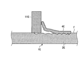
- the contact portion is formed by the method of Patent Document 1, as shown in FIG. 1A, the contact portion 4E is formed so as to rise from the sliding surface f of the molded circuit component 1E, and the contact terminal 11E is connected to the contact portion.
- the contact terminal 11E is applied to the side surface of the contact portion 4E.
- the contact part 4E may be peeled off from the sliding surface f of the molded circuit component 1E by repeating the sliding operation (see FIG. 1B).
- the present invention has been made in view of the above, and when used in a connection structure that is electrically connected by sliding, it can suppress peeling of the circuit portion that functions as a contact portion,
- An object of the present invention is to provide a molded circuit component having high durability and an electrical connection structure.
- the molded circuit component according to the present invention is a molded circuit component used as a fixed contact of an electrical connection structure having a sliding contact and a fixed contact.
- a concave portion is formed on the sliding surface of the circuit component, and a circuit portion serving as a contact portion is provided on the bottom surface of the concave portion.
- the molded circuit component of the present invention is characterized in that, in the above invention, the height from the bottom surface of the recess to the surface of the contact portion is not more than the height from the bottom surface of the recess to the sliding surface. .
- the molded circuit component of the present invention is characterized in that, in the above invention, the outer shape of the concave portion is larger than the outer shape of the contact portion.
- the molded circuit component of the present invention is characterized in that, in the above invention, the side surface of the recess has an inclination.
- the electrical connection structure of the present invention comprises a molded circuit component according to any one of the above, wherein the sliding surface includes a recess, and a contact portion formed on the bottom surface of the recess functions as a fixed contact.
- the molded circuit includes a contact terminal that is in contact with and electrically connected to the contact portion, and a holding portion that holds the contact terminal, and presses the contact terminal in a direction orthogonal to the sliding surface. And a sliding contact that slides on the sliding surface of the component in a direction parallel to the sliding surface.
- the contact terminal has a shape that does not contact the side surface of the contact portion when the sliding contact is slid from the surface of the molded circuit component into the recess. It is characterized by doing.
- the contact terminal has a columnar shape, and a bottom surface having the same shape as a cross-sectional shape of the contact terminal in a direction parallel to the sliding surface is in contact with the contact portion.
- the length of the contact surface in the sliding direction is not less than the length from the end of the contact portion to the side surface of the recess in the sliding direction at the surface height of the contact portion.
- the contact terminal has a columnar shape, an end portion on the side in contact with the contact portion has a convex shape, and a contact surface in contact with the contact portion is formed.
- the sum of the length in the sliding direction and the length of the outer peripheral portion of the contact surface is not less than the length from the end of the contact portion to the upper end of the recess in the sliding direction at the height of the sliding surface. It is characterized by being.
- the electrical connection structure of the present invention is the above-described invention, wherein the contact terminal is columnar and the end portion on the side in contact with the contact portion has an arc shape, and the radius of the contact terminal is a sliding surface It is more than the length from the edge part of the contact part in the sliding direction in the height to the upper end part of a recessed part, It is characterized by the above-mentioned.
- the contact portion in the concave portion, it is possible to prevent the contact portion from being peeled off by applying the contact terminal to the side surface of the contact portion.
- FIG. 1A is a diagram for explaining a case where a molded circuit component manufactured by a conventional technique is used for an electrical connection structure.
- FIG. 1B is a diagram for explaining a case where a molded circuit component manufactured by a conventional technique is used for an electrical connection structure.
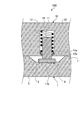
- FIG. 2 is a cross-sectional view of an electrical connection structure using the molded circuit component according to the first embodiment of the present invention.
- FIG. 3 is a perspective view of an electrical connection structure using the molded circuit component according to the first embodiment of the present invention.
- FIG. 4 is a cross-sectional view for explaining the configuration of the concave portion of the molded circuit component according to the first embodiment of the present invention.
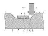
- FIG. 5A is a cross-sectional view for explaining sliding of the contact terminal when the molded circuit component according to the first exemplary embodiment of the present invention is used in the electrical connection structure.
- FIG. 5B is a cross-sectional view for explaining sliding of the contact terminal when the molded circuit component according to Embodiment 1 of the present invention is used in the electrical connection structure.
- FIG. 5C is a cross-sectional view illustrating sliding of the contact terminals when the molded circuit component according to Embodiment 1 of the present invention is used for an electrical connection structure.
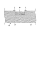
- FIG. 6 is a cross-sectional view for explaining the configuration of the concave portion of the molded circuit component according to the modification of the first embodiment of the present invention.
- FIG. 7 is a cross-sectional view of the electrical connection structure according to the second embodiment of the present invention.
- FIG. 8 is a cross-sectional view of the electrical connection structure according to the third embodiment of the present invention.
- FIG. 2 is a cross-sectional view of an electrical connection structure using the molded circuit component according to the first embodiment of the present invention.
- FIG. 3 is a perspective view of an electrical connection structure using the molded circuit component according to the first embodiment of the present invention.
- the electrical connection structure 100 according to the first embodiment includes a molded circuit component 1 that functions as a fixed contact and a sliding contact 10.
- the molded circuit component 1 includes a main body 2 having a three-dimensional circuit formed on the surface, a recess 3 formed on the sliding surface f of the main body 2, and a bottom surface of the recess 3.
- the contact part 4 and the circuit part 5 which are electrically connected are provided.
- the main body 2 is formed by molding a non-conductive resin material such as a liquid crystal polymer or polycarbonate into a desired shape by injection molding.
- the recess 3 is formed when the main body 2 is injection molded.
- the resin material constituting the main body 2 includes carrier particles that carry a heavy metal complex salt on a microporous or microrough surface. After molding a resin material containing carrier particles supporting a heavy metal complex salt, the surface of the main body part 2 is ablated by irradiation with electromagnetic radiation, the heavy metal complex salt is decomposed to generate a heavy metal nucleus, and then the contact part 4 and the circuit are formed by plating. Part 5 is formed.
- a known method for producing a molded circuit component for example, Japanese Patent No. 336652 can be referred to.
- the sliding contact 10 is in contact with the contact portion 4 and electrically connected thereto, the holding portion 12 holding the contact terminal 11, and the holding portion 12 orthogonal to the sliding surface f of the molded circuit component 1.
- a drive unit (not shown) that slides the contact terminal 11 on the sliding surface f of the molded circuit component 1 by moving in the direction perpendicular to the sliding surface f while pressing in the direction.
- the contact terminal 11 has a cylindrical shape, and the bottom surface is a contact surface 11 b that contacts the contact portion 4.
- a flange portion 11a is formed on the contact surface 11b side.
- the holding part 12 has a groove part 13 for accommodating the contact terminal 11 on the surface in contact with the molded circuit component 1.
- a positioning portion 13a is formed at the opening end of the groove portion 13, and the contact terminal 11 is positioned by engaging the flange portion 11a with the positioning portion 13a.
- the contact terminal 11 is pressed against the opening end side of the groove 13 by the spring member 14 and comes into contact with the sliding surface f of the molded circuit component 1 and the contact portion 4.
- FIG. 3 when the contact terminal 11 is in contact with the surface of the main body 2 made of a non-conductive resin material, it is not electrically connected, and the contact terminal 11 is slid by sliding the sliding contact 10. Is in electrical contact with the contact portion 4.
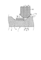
- FIG. 4 is a cross-sectional view illustrating the configuration of the recess 3 of the molded circuit component 1 according to the first embodiment of the present invention.
- 5A to 5C are cross-sectional views illustrating sliding of the contact terminals 11 when the molded circuit component 1 according to the first embodiment of the present invention is used in the electrical connection structure 100.
- FIG. 4 is a cross-sectional view illustrating the configuration of the recess 3 of the molded circuit component 1 according to the first embodiment of the present invention.
- 5A to 5C are cross-sectional views illustrating sliding of the contact terminals 11 when the molded circuit component 1 according to the first embodiment of the present invention is used in the electrical connection structure 100.
- FIG. 4 is a cross-sectional view illustrating the configuration of the recess 3 of the molded circuit component 1 according to the first embodiment of the present invention.
- 5A to 5C are cross-sectional views illustrating sliding of the contact terminals 11 when the molded circuit component 1 according to the first embodiment of the present invention is used in the
- the height t 2 of the recess 3, that is, the height t 2 of the bottom surface 3b to the sliding surface f of the molded circuit component 1 of the recess 3, the height t 1 of the contact portion 4, or recess 3 is preferably a height t 1 or more from the bottom surface 3 b of the contact 3 to the surface 4 a of the contact portion 4.
- the side surface 3a of the recess 3 is preferably an inclined surface.
- the contact terminal 11 can be smoothly slid by making the side surface 3a in contact with the inclined surface.
- the contact surface of the contact terminal 11 is a plane parallel to the surface 4a of the contact portion 4, the effect of making the contacting side surface 3a as an inclined surface is great, and the contact terminal 11 can be smoothly slid.
- a part of the outer peripheral surface of the contact surface 11 b is recessed 3 as shown in FIG. 5B. In a state in which it is in contact with the side surface 3a and pressed downward in the vertical direction by the spring member 14, it slides to the left as indicated by the arrow in FIG. 5B.
- the contact terminal 11 has a shape that does not come into contact with the side surface 4b of the contact portion 4 when the contact terminal 11 is slid into the recess 3 from the surface of the molded circuit component 1, that is, the contact surface 11b is a contact terminal.
- 11 has the same shape as the horizontal cross-sectional shape, and the length r 2 of the contact surface 11b in the sliding direction is the end of the contact portion 4 in the sliding direction at the height of the surface 4a of the contact portion 4. is the length r 1 or more to the intersection 3d side 3a of the virtual line and the concave portion 3 that extends in the sliding direction from 4c.
- the outer shape of the concave portion 3 is preferably larger than the outer shape of the contact portion 4 in consideration of the accuracy of electromagnetic radiation when forming the contact portion 4 in the concave portion 3.
- the outer shapes of the concave portion 3 and the contact portion 4 are substantially the same, there is a possibility that the metal plating 6 is formed outside the concave portion 4 as shown in FIG.
- the contact portion 4A formed in the recess 3A is prevented from being peeled off by sliding of the contact terminals, but the metal plating 6 causes the sliding surface f to be convex and smooth.
- the outer shape of the concave portion 3 is larger than the outer shape of the contact portion 4 because there is a risk of inhibiting the sliding.
- FIG. 7 is a cross-sectional view of the electrical connection structure according to the second embodiment of the present invention.
- the end of the contact terminal 11B on the side in contact with the contact part 4 has an arc shape.
- the contact terminal 11B is in electrical contact with the contact portion 4 at a contact point 11b 'serving as a vertex.
- the contact terminal 11B slides smoothly even when there is a height difference between the surface 4a of the contact portion 4 and the sliding surface f because the end on the side in contact with the contact portion 4 has an arc shape. be able to.
- the end of the contact terminal 11 ⁇ / b> B on the side in contact with the contact portion 4 has a shape that does not come into contact with the side surface 4 b of the contact portion 4 when it is slid into the recess 3 from the surface of the molded circuit component 1.
- End of the contact terminal 11B which is in contact with the contact portion 4 the end portion 4c of the surface 4a in the sliding direction, a arc shape passing through the upper portion 3c of recess 3, the radius r 4 of the contact pin 11B is , the recess 3 of the upper end portion to 3c length r 3 or more from the end portion 4c of the contact portion 4 in the sliding direction of the height of the sliding surface f.
- the contact terminal 11B contacts the surface 4a of the contact part 4 without contacting the side surface 4b of the contact part 4, the contact part 4 is prevented from peeling and the arc-shaped end part of the contact terminal 11B is centered. Therefore, a stable contact function can be maintained without wearing asymmetrically.
- the edge part of the side in contact with the contact part 4 of the contact terminal 11B should just be a convex curve shape, and is not limited to circular arc shape. If convex surface is not a circular arc shape, taking the radius r 4 based on the lowest point of the contact terminal 11B (point closest to the bottom surface of the recess).
- FIG. 8 is a cross-sectional view of the electrical connection structure according to the third embodiment of the present invention. In FIG. 8, illustration of a holding part etc. is omitted for convenience.
- the end on the side in contact with the contact part 4 has a truncated cone shape.
- the end portion of the contact terminal 11D on the side in contact with the contact portion 4 has a shape that does not come into contact with the side surface 4b of the contact portion 4 when being slid into the recess 3 from the surface of the molded circuit component 1.
- the contact terminal 11D contacts the surface 4a of the contact part 4 without contacting the side surface 4b of the contact part 4, so that the contact part 4 is prevented from peeling and the end of the contact terminal 11D is not targeted from the center.
- a stable contact function can be maintained without being worn.
- each embodiment has been described.
- the contact terminal is formed in the concave portion by forming the contact portion in the concave portion. Stress at the time of contact with the side surface is easily reduced, and the effect of suppressing peeling of the contact portion is exhibited. The effect is particularly remarkable when the contact terminals to be used are convex.
- the shape of the end of the contact terminal on the side in contact with the contact portion ensures electrical connection with the contact portion.
- the contact terminal Is not limited to the shape of Embodiments 1 to 3 above, and the effect of suppressing peeling is further enhanced.
- the molded circuit component and the electrical connection structure according to the present invention are useful for a contact portion of an electronic component that involves sliding, and particularly for a dial switch, a mode changeover switch, and a lens mounting portion of a digital camera or the like. Is suitable.
Landscapes
- Coupling Device And Connection With Printed Circuit (AREA)
- Manufacturing Of Electrical Connectors (AREA)
- Contacts (AREA)
Abstract
摺動により電気的に接続される接続構造に使用される際にも、接点部として機能する回路部の剥離を抑制することができ、耐久性の高い成形回路部品、および電気的接続構造を提供する。本発明における成形回路部品1は、摺動接点と固定接点とを有する電気的接続構造の固定接点として使用される成形回路部品1において、摺動面fに凹部3を備え、凹部3の底面3bに接点部4が形成されることを特徴とする。
Description
本発明は、成形回路部品、および前記成形回路部品を使用する電気的接続構造に関する。
近年、デバイスの小型化、ならびに部品点数および組み立て工数の削減を目的として、三次元構造の本体部に三次元回路が形成された成形回路部品(Molded Interconnect Device、以下「MID」という)が電子部品として使用されている。
成形回路部品の使用用途として、例えば、成形回路部品の表面に形成された回路部を、スイッチの摺動接点部として使用できることが開示されている(例えば、特許文献1参照)。
特許文献1では、成形回路部品の下地処理をウエットブラスト法で行うことにより、平滑なめっき面を形成できるとしている。しかしながら、特許文献1の方法で接点部を形成した場合、図1Aに示すように、接点部4Eは成形回路部品1Eの摺動面fから盛り上がるように形成されており、接触端子11Eを接点部4Eの方に摺動させると、接点部4Eの側面に接触端子11Eが当て付けられる。このため、摺動動作の繰り返しにより、接点部4Eが成形回路部品1Eの摺動面fから剥離するおそれがある(図1B参照)。
本発明は、上記に鑑みてなされたものであって、摺動により電気的に接続される接続構造に使用される際にも、接点部として機能する回路部の剥離を抑制することができ、耐久性の高い成形回路部品、および電気的接続構造を提供することを目的とする。
上述した課題を解決し、目的を達成するために、本発明にかかる成形回路部品は、摺動接点と固定接点とを有する電気的接続構造の固定接点として使用される成形回路部品において、前記成形回路部品の摺動面に凹部が形成され、前記凹部の底面に接点部となる回路部が設けられることを特徴とする。
また、本発明の成形回路部品は、上記発明において、前記凹部の底面から前記接点部表面までの高さは、前記凹部の底面から前記摺動面までの高さ以下であることを特徴とする。
また、本発明の成形回路部品は、上記発明において、前記凹部の外形は、前記接点部の外形より大きいことを特徴とする。
また、本発明の成形回路部品は、上記発明において、前記凹部の側面は傾斜を有することを特徴とする。
また、本発明の電気的接続構造は、前記摺動面に凹部を備え、前記凹部の底面に形成された接点部が固定接点として機能する上記のいずれか一つに記載の成形回路部品と、前記接点部と接触して電気的に接続する接触端子と、前記接触端子を保持する保持部と、を有し、前記接触端子を前記摺動面と直交する方向に押圧しながら、前記成形回路部品の摺動面上を摺動面と平行方向に摺動させる摺動接点と、を備えることを特徴とする。
また、本発明の電気的接続構造は、上記発明において、前記接触端子は、前記摺動接点を前記成形回路部品の表面から凹部内に摺動させる際、前記接点部の側面と接触しない形状をなすことを特徴とする。
また、本発明の電気的接続構造は、上記発明において、前記接触端子が柱状であって、前記摺動面と平行方向の前記接触端子の断面形状と同一形状の底面が前記接点部と接する接触面をなし、前記接触面の摺動方向の長さは、前記接点部の表面高さにおける摺動方向での前記接点部の端部から前記凹部の側面までの長さ以上であることを特徴とする。
また、本発明の電気的接続構造は、上記発明において、前記接触端子が柱状であって、前記接点部と接触する側の端部が凸部形状であり、前記接点部と接触する接触面の摺動方向の長さと前記接触面の外周部の長さの和は、前記摺動面の高さにおける摺動方向での前記接点部の端部から前記凹部の上端部までの長さ以上であることを特徴とする。
また、本発明の電気的接続構造は、上記発明において、前記接触端子が柱状、かつ、前記接点部との接触する側の端部形状が円弧状をなし、接触端子の半径は、摺動面の高さにおける摺動方向での接点部の端部から凹部の上端部までの長さ以上であることを特徴とする。
本発明では、接点部を凹部内に形成することにより、接点部の側面への接触端子の当て付けによる接点部の剥離を防止することができる。
以下の説明では、本発明を実施するための形態(以下、「実施の形態」という)として、成形回路部品および成形回路部品を用いた回路モジュールについて説明する。また、この実施の形態により、この発明が限定されるものではない。さらに、図面の記載において、同一部分には同一の符号を付している。さらにまた、図面は、模式的なものであり、各部材の厚みと幅との関係、各部材の比率等は、現実と異なることに留意する必要がある。また、図面の相互間においても、互いの寸法や比率が異なる部分が含まれている。
(実施の形態1)
図2は、本発明の実施の形態1にかかる成形回路部品を用いた電気的接続構造の断面図である。図3は、本発明の実施の形態1にかかる成形回路部品を用いた電気的接続構造の斜視図である。実施の形態1にかかる電気的接続構造100は、固定接点として機能する成形回路部品1と摺動接点10とを備える。
図2は、本発明の実施の形態1にかかる成形回路部品を用いた電気的接続構造の断面図である。図3は、本発明の実施の形態1にかかる成形回路部品を用いた電気的接続構造の斜視図である。実施の形態1にかかる電気的接続構造100は、固定接点として機能する成形回路部品1と摺動接点10とを備える。
成形回路部品1は、三次元回路が表面に形成された本体部2と、本体部2の摺動面fに形成された凹部3と、凹部3の底面上に設けられ、摺動接点10と電気的に接続される接点部4と、回路部5とを備える。
本体部2は、例えば液晶ポリマー、ポリカーボネートなどの非導電性の樹脂材料を射出成型により所望の形状に成形したものである。凹部3は、本体部2を射出成型する際に形成される。本体部2を構成する樹脂材料は、重金属錯塩を微小多孔質または微小粗面に担持する担体粒子を含む。重金属錯塩を担持する担体粒子を含有する樹脂材料を成形した後、電磁線照射により本体部2の表面をアブレーションし、重金属錯塩を分解して重金属核を生成した後、めっきにより接点部4および回路部5を形成する。回路形成は、公知の成形回路部品の製造方法、たとえば、特許第3366652号公報等を参照することができる。
摺動接点10は、接点部4と接触して電気的に接続する接触端子11と、接触端子11を保持する保持部12と、保持部12を成形回路部品1の摺動面fと直交する方向に押圧しながら摺動面fと垂直方向に移動することにより、接触端子11を成形回路部品1の摺動面f上を摺動させる図示しない駆動部とを備える。接触端子11は円柱状をなし、底面が接点部4と接触する接触面11bとなる。接触端子11の側面には、接触面11b側にフランジ部11aが形成されている。
保持部12は、成形回路部品1と接する面に、接触端子11を収容する溝部13を有する。溝部13の開口端には位置止部13aが形成され、接触端子11はフランジ部11aが位置止部13aに係合されて位置止めされる。接触端子11は、バネ部材14により溝部13の開口端側に押圧され、成形回路部品1の摺動面fおよび接点部4と接触する。図3に示すように、接触端子11が非導電性の樹脂材料からなる本体部2の表面に接触している場合は電気的に接続されず、摺動接点10を摺動して接触端子11が接点部4と接触すると、電気的に接続される。なお、図3では、便宜上保持部12等の図示を省略している。
次に凹部3の形状について、図を参照して説明する。図4は、本発明の実施の形態1にかかる成形回路部品1の凹部3の構成を説明する断面図である。図5A~図5Cは、本発明の実施の形態1にかかる成形回路部品1を電気的接続構造100に使用した場合の接触端子11の摺動を説明する断面図である。
図4に示すように、凹部3の高さt2、すなわち凹部3の底面3bから成形回路部品1の摺動面fまでの高さt2は、接点部4の高さt1、すなわち凹部3の底面3bから接点部4の表面4aまでの高さt1以上であることが好ましい。凹部3の高さt2を接点部4の高さt1以上とすることにより、摺動接点10を摺動させた際に、接触端子11が接点部4の側面4bに接触しないため、接点部4の剥離を防止できるためである。
また、凹部3の側面3aは、傾斜面とすることが好ましい。摺動接点10が摺動する際、接触する側面3aを傾斜面とすることにより接触端子11を滑らかに摺動させることができる。特に、接触端子11の接触面が接点部4の表面4aと平行な平面である場合、接触する側面3aを傾斜面とする効果が大きく、接触端子11の滑らかな摺動が可能となる。接触端子11は、本体部2の表面に接触した状態から、図5A中の矢印で示す左側に摺動されると、図5Bに示すように、接触面11bの外周面の一部が凹部3の側面3aと接触した状態で、バネ部材14により鉛直方向下方に押圧された状態で、図5B中の矢印で示す左側に摺動する。
さらに、図5Cに示すように、接触端子11は、成形回路部品1の表面から凹部3内に摺動させた際、接点部4の側面4bと接触しない形状、すなわち、接触面11bは接触端子11の水平方向の断面形状と同一形状であって、接触面11bの摺動方向の長さr2、は、接点部4の表面4aの高さにおける摺動方向での接点部4の端部4cから摺動方向に延長した仮想線と凹部3の側面3aの交点3dまでの長さr1以上である。接触端子11の形状を上記のようにすることにより、接触端子11が接点部4の側面4bに接触しないため、接点部4の剥離を防止できる。
なお、凹部3内に接点部4を形成する際の電磁線照射の精度等を考慮すると、凹部3の外形は接点部4の外形より大きくすることが好ましい。凹部3と接点部4の外形を略同一にした場合、電磁線照射の位置ずれにより意図しない部分、例えば、図6に示すように、凹部4外に金属めっき6が形成されるおそれがある。図6に示す成形回路部品1Aにおいても、凹部3A内に形成される接点部4Aは接触端子の摺動による剥離が抑制されるが、金属めっき6により摺動面fに凸が生じ、滑らかな摺動を阻害するおそれがあるため、凹部3の外形は接点部4の外形より大きくすることが好ましい。
(実施の形態2)
図7は、本発明の実施の形態2にかかる電気的接続構造の断面図である。実施の形態2にかかる電気的接続構造100Bにおいて、接触端子11Bの接点部4と接する側の端部は円弧状をなしている。
図7は、本発明の実施の形態2にかかる電気的接続構造の断面図である。実施の形態2にかかる電気的接続構造100Bにおいて、接触端子11Bの接点部4と接する側の端部は円弧状をなしている。
接触端子11Bは、頂点となる接触点11b’で接点部4と電気的に接触する。接触端子11Bは、接点部4と接する側の端部が円弧状をなしているため、接点部4の表面4aと摺動面fとの間に高低差がある場合にも滑らかに摺動することができる。
接触端子11Bの接点部4と接する側の端部は、成形回路部品1の表面から凹部3内に摺動させた際、接点部4の側面4bと接触しない形状である。接点部4と接する側の接触端子11Bの端部は、摺動方向における表面4aの端部4cと、凹部3の上端部3cとを通る円弧状であって、接触端子11Bの半径r4は、摺動面fの高さにおける摺動方向での接点部4の端部4cから凹部3の上端部3cまでの長さr3以上とする。これにより、接触端子11Bは、接点部4の側面4bに接することなく接点部4の表面4aに接触するため、接点部4の剥離を抑制するとともに、接触端子11Bの円弧状の端部が中心から非対称に摩耗することなく安定した接触機能を保つことができる。
また、接触端子11Bの接点部4と接する側の端部は、凸曲面形状であればよく、円弧状に限定されるものではない。円弧形状ではない凸曲面の場合、接触端子11Bの最も低い点(凹部底面に最も近い点)を基準に半径r4をとる。
(実施の形態3)
図8は、本発明の実施の形態3にかかる電気的接続構造の断面図である。図8では、便宜上保持部等の図示を省略している。
図8は、本発明の実施の形態3にかかる電気的接続構造の断面図である。図8では、便宜上保持部等の図示を省略している。
本発明の実施の形態3にかかる接触端子11Dは、接点部4と接する側の端部が円錐台状をなしている。
接触端子11Dの接点部4と接する側の端部は、成形回路部品1の表面から凹部3内に摺動させた際、接点部4の側面4bと接触しない形状である。接触端子11Dの接点部4と接触する接触面11bの摺動方向の長さr2と接触面11bの外周側面11cの長さr5の和は、摺動面fの高さにおける摺動方向での接点部4の端部4cから凹部3の上端部3cまでの長さr4以上とする。これにより、接触端子11Dは、接点部4の側面4bに接することなく接点部4の表面4aに接触するため、接点部4の剥離を抑制するとともに、接触端子11Dの端部が中心から非対象に摩耗することなく安定した接触機能を保つことができる。
以上、各実施形態を説明してきたが、成形回路部品は、凹部の高さが接点部の高さより小さい場合であっても、凹部内に接点部を形成することにより、接触端子が接点部の側面に接触する際の応力が低減されやすくなり、接点部の剥離抑制効果を発揮する。特に利用する接触端子が凸形状のときに顕著に効果を発揮する。
なお、接触端子の接点部と接する側の端部の形状は、接点部との電気的な接続が確保でき、摺動接点を成形回路部品の表面から凹部内に摺動させた際、接触端子が接点部の側面と接触しないものであれば、上記の実施形態1~3の形状に限定されず、さらに剥離抑制効果が高まる。
以上のように、本発明にかかる成形回路部品および電気的接続構造は、摺動を伴う電子部品の接点部に有用であり、特に、デジタルカメラ等のダイヤルスイッチ、モード切替スイッチ、レンズ取付け部に適している。
1、1A、1E 成形回路部品
2、2A、2E 本体部
3、3A 凹部
3a 側面
3b 底面
3c 上端部
3d 摺動方向に延長した仮想線と凹部3の側面上の交点
4、4A、4E 接点部
4a 表面
4b 側面
4c 端部
5 回路部
6 金属めっき
10 摺動接点
11、11B、11D、11E 接触端子
11a フランジ部
11b 接触面
11b’ 接触点
11c 外周側面
12、12B 保持部
13、13B 溝部
13a 位置止部
14、14B バネ部材
100、100B 電気的接続構造
2、2A、2E 本体部
3、3A 凹部
3a 側面
3b 底面
3c 上端部
3d 摺動方向に延長した仮想線と凹部3の側面上の交点
4、4A、4E 接点部
4a 表面
4b 側面
4c 端部
5 回路部
6 金属めっき
10 摺動接点
11、11B、11D、11E 接触端子
11a フランジ部
11b 接触面
11b’ 接触点
11c 外周側面
12、12B 保持部
13、13B 溝部
13a 位置止部
14、14B バネ部材
100、100B 電気的接続構造
Claims (9)
- 摺動接点と固定接点とを有する電気的接続構造の固定接点として使用される成形回路部品において、
前記成形回路部品の摺動面に凹部が形成され、前記凹部の底面に接点部となる回路部が設けられることを特徴とする成形回路部品。 - 前記凹部の底面から前記接点部表面までの高さは、前記凹部の底面から前記摺動面までの高さ以下であることを特徴とする請求項1に記載の成形回路部品。
- 前記凹部の外形は、前記接点部の外形より大きいことを特徴とする請求項1または2に記載の成形回路部品。
- 前記凹部の側面は傾斜を有することを特徴とする請求項1~3のいずれか一つに記載の成形回路部品。
- 前記摺動面に凹部が形成され、前記凹部の底面に設けられた接点部が固定接点として機能する請求項1~4のいずれか一つに記載の成形回路部品と、
前記接点部と接触して電気的に接続する接触端子と、前記接触端子を保持する保持部と、を有し、前記接触端子を前記摺動面と直交する方向に押圧しながら、前記成形回路部品の摺動面上を摺動面と平行方向に摺動させる摺動接点と、を備えることを特徴とする電気的接続構造。 - 前記接触端子は、前記摺動接点を前記成形回路部品の表面から凹部内に摺動させる際、前記接点部の側面と接触しない形状をなすことを特徴とする請求項5に記載の電気的接続構造。
- 前記接触端子が柱状であって、摺動面と平行方向の前記接触端子の断面形状と同一形状の底面が前記接点部と接する接触面をなし、
前記接触面の摺動方向の長さは、前記接点部の表面高さにおける摺動方向での前記接点部の端部から前記凹部の側面までの長さ以上であることを特徴とする請求項6に記載の電気的接続構造。 - 前記接触端子が柱状であって、前記接点部と接触する側の端部が凸部形状であり、
前記接点部と接触する接触面の摺動方向の長さと前記接触面の外周部の摺動方向の長さの和は、前記摺動面の高さにおける摺動方向での前記接点部の端部から前記凹部の上端部までの長さ以上であることを特徴とする請求項6に記載の電気的接続構造。 - 前記接触端子が柱状、かつ、前記接点部との接触する側の端部形状が円弧状をなし、接触端子の半径は、摺動面の高さにおける摺動方向での接点部の端部から凹部の上端部までの長さ以上であることを特徴とする請求項6または8に記載の電気的接続構造。
Applications Claiming Priority (2)
| Application Number | Priority Date | Filing Date | Title |
|---|---|---|---|
| JP2015-093386 | 2015-04-30 | ||
| JP2015093386A JP2016213003A (ja) | 2015-04-30 | 2015-04-30 | 成形回路部品、および電気的接続構造 |
Publications (1)
| Publication Number | Publication Date |
|---|---|
| WO2016174937A1 true WO2016174937A1 (ja) | 2016-11-03 |
Family
ID=57199312
Family Applications (1)
| Application Number | Title | Priority Date | Filing Date |
|---|---|---|---|
| PCT/JP2016/057382 Ceased WO2016174937A1 (ja) | 2015-04-30 | 2016-03-09 | 成形回路部品、および電気的接続構造 |
Country Status (2)
| Country | Link |
|---|---|
| JP (1) | JP2016213003A (ja) |
| WO (1) | WO2016174937A1 (ja) |
Citations (3)
| Publication number | Priority date | Publication date | Assignee | Title |
|---|---|---|---|---|
| JPS5076373U (ja) * | 1973-11-15 | 1975-07-03 | ||
| JPH08339734A (ja) * | 1995-06-12 | 1996-12-24 | Tokai Rika Hanbai Kk | スイッチ装置 |
| JP2011210452A (ja) * | 2010-03-29 | 2011-10-20 | Panasonic Electric Works Asahi Co Ltd | 回転スイッチ |
Family Cites Families (3)
| Publication number | Priority date | Publication date | Assignee | Title |
|---|---|---|---|---|
| JPS5710033Y2 (ja) * | 1974-10-16 | 1982-02-26 | ||
| JPS5855629B2 (ja) * | 1975-12-31 | 1983-12-10 | 松下電工株式会社 | ブラシソウチ |
| JPS56115887U (ja) * | 1980-02-06 | 1981-09-05 |
-
2015
- 2015-04-30 JP JP2015093386A patent/JP2016213003A/ja active Pending
-
2016
- 2016-03-09 WO PCT/JP2016/057382 patent/WO2016174937A1/ja not_active Ceased
Patent Citations (3)
| Publication number | Priority date | Publication date | Assignee | Title |
|---|---|---|---|---|
| JPS5076373U (ja) * | 1973-11-15 | 1975-07-03 | ||
| JPH08339734A (ja) * | 1995-06-12 | 1996-12-24 | Tokai Rika Hanbai Kk | スイッチ装置 |
| JP2011210452A (ja) * | 2010-03-29 | 2011-10-20 | Panasonic Electric Works Asahi Co Ltd | 回転スイッチ |
Also Published As
| Publication number | Publication date |
|---|---|
| JP2016213003A (ja) | 2016-12-15 |
Similar Documents
| Publication | Publication Date | Title |
|---|---|---|
| JP5881666B2 (ja) | リセプタクルコネクタの製造方法 | |
| US9703173B2 (en) | Camera module structure having electronic device connections formed therein | |
| JP2022033394A (ja) | 基板接続コネクタ | |
| JP6074402B2 (ja) | 3d立体回路構造の端子脚に板バネが結合された構造 | |
| JP4710627B2 (ja) | 基板間接続コネクタ | |
| JP6133258B2 (ja) | 防水コネクタ | |
| KR200489678Y1 (ko) | 박막형 마그네틱 커넥터 모듈 | |
| JP2023036857A (ja) | 基板接続コネクタ向けの端子、コネクタ及びコネクタ製造方法 | |
| US20190006779A1 (en) | Connector terminal assembly | |
| US8460014B2 (en) | Electronic device and pin thereof | |
| US8761595B2 (en) | Camera including mount for flash | |
| KR20160138666A (ko) | 전자 장치 | |
| KR20160005084A (ko) | 전자 장치 | |
| JP6974556B2 (ja) | 基板接続コネクタ向けの端子、コネクタ及びコネクタ製造方法 | |
| KR20160090018A (ko) | 카메라 모듈 | |
| CN113708117B (zh) | 电连接器组合 | |
| WO2016174937A1 (ja) | 成形回路部品、および電気的接続構造 | |
| US20140050469A1 (en) | Camera module | |
| US20150138420A1 (en) | Liquid crystal cell connection to lens mount of camera module | |
| JP2011233485A (ja) | スパイラル状接触子を備えた電子部品 | |
| JP6055939B2 (ja) | リセプタクルコネクタ及びリセプタクルコネクタの製造方法 | |
| CN1319217C (zh) | 用于便携式电话机的压接触型连接器及其连接结构 | |
| US9059544B2 (en) | Electrical connector | |
| KR102040290B1 (ko) | 탄성 전기단자의 장착 구조 | |
| JP6150854B2 (ja) | リセプタクルコネクタ |
Legal Events
| Date | Code | Title | Description |
|---|---|---|---|
| 121 | Ep: the epo has been informed by wipo that ep was designated in this application |
Ref document number: 16786214 Country of ref document: EP Kind code of ref document: A1 |
|
| NENP | Non-entry into the national phase |
Ref country code: DE |
|
| 122 | Ep: pct application non-entry in european phase |
Ref document number: 16786214 Country of ref document: EP Kind code of ref document: A1 |