WO2016167285A1 - 構造制御されたハロゲン化金属結晶とペロブスカイト化合物結晶 - Google Patents
構造制御されたハロゲン化金属結晶とペロブスカイト化合物結晶 Download PDFInfo
- Publication number
- WO2016167285A1 WO2016167285A1 PCT/JP2016/061905 JP2016061905W WO2016167285A1 WO 2016167285 A1 WO2016167285 A1 WO 2016167285A1 JP 2016061905 W JP2016061905 W JP 2016061905W WO 2016167285 A1 WO2016167285 A1 WO 2016167285A1
- Authority
- WO
- WIPO (PCT)
- Prior art keywords
- metal halide
- crystal
- perovskite compound
- general formula
- crystals
- Prior art date
- Legal status (The legal status is an assumption and is not a legal conclusion. Google has not performed a legal analysis and makes no representation as to the accuracy of the status listed.)
- Ceased
Links
Images




Classifications
-
- C—CHEMISTRY; METALLURGY
- C07—ORGANIC CHEMISTRY
- C07F—ACYCLIC, CARBOCYCLIC OR HETEROCYCLIC COMPOUNDS CONTAINING ELEMENTS OTHER THAN CARBON, HYDROGEN, HALOGEN, OXYGEN, NITROGEN, SULFUR, SELENIUM OR TELLURIUM
- C07F7/00—Compounds containing elements of Groups 4 or 14 of the Periodic Table
- C07F7/24—Lead compounds
-
- D—TEXTILES; PAPER
- D01—NATURAL OR MAN-MADE THREADS OR FIBRES; SPINNING
- D01D—MECHANICAL METHODS OR APPARATUS IN THE MANUFACTURE OF ARTIFICIAL FILAMENTS, THREADS, FIBRES, BRISTLES OR RIBBONS
- D01D5/00—Formation of filaments, threads, or the like
- D01D5/08—Melt spinning methods
-
- D—TEXTILES; PAPER
- D01—NATURAL OR MAN-MADE THREADS OR FIBRES; SPINNING
- D01F—CHEMICAL FEATURES IN THE MANUFACTURE OF ARTIFICIAL FILAMENTS, THREADS, FIBRES, BRISTLES OR RIBBONS; APPARATUS SPECIALLY ADAPTED FOR THE MANUFACTURE OF CARBON FILAMENTS
- D01F1/00—General methods for the manufacture of artificial filaments or the like
- D01F1/02—Addition of substances to the spinning solution or to the melt
-
- D—TEXTILES; PAPER
- D01—NATURAL OR MAN-MADE THREADS OR FIBRES; SPINNING
- D01F—CHEMICAL FEATURES IN THE MANUFACTURE OF ARTIFICIAL FILAMENTS, THREADS, FIBRES, BRISTLES OR RIBBONS; APPARATUS SPECIALLY ADAPTED FOR THE MANUFACTURE OF CARBON FILAMENTS
- D01F6/00—Monocomponent artificial filaments or the like of synthetic polymers; Manufacture thereof
- D01F6/44—Monocomponent artificial filaments or the like of synthetic polymers; Manufacture thereof from mixtures of polymers obtained by reactions only involving carbon-to-carbon unsaturated bonds as major constituent with other polymers or low-molecular-weight compounds
- D01F6/50—Monocomponent artificial filaments or the like of synthetic polymers; Manufacture thereof from mixtures of polymers obtained by reactions only involving carbon-to-carbon unsaturated bonds as major constituent with other polymers or low-molecular-weight compounds of polyalcohols, polyacetals or polyketals
-
- D—TEXTILES; PAPER
- D01—NATURAL OR MAN-MADE THREADS OR FIBRES; SPINNING
- D01F—CHEMICAL FEATURES IN THE MANUFACTURE OF ARTIFICIAL FILAMENTS, THREADS, FIBRES, BRISTLES OR RIBBONS; APPARATUS SPECIALLY ADAPTED FOR THE MANUFACTURE OF CARBON FILAMENTS
- D01F9/00—Artificial filaments or the like of other substances; Manufacture thereof; Apparatus specially adapted for the manufacture of carbon filaments
- D01F9/08—Artificial filaments or the like of other substances; Manufacture thereof; Apparatus specially adapted for the manufacture of carbon filaments of inorganic material
-
- D—TEXTILES; PAPER
- D04—BRAIDING; LACE-MAKING; KNITTING; TRIMMINGS; NON-WOVEN FABRICS
- D04H—MAKING TEXTILE FABRICS, e.g. FROM FIBRES OR FILAMENTARY MATERIAL; FABRICS MADE BY SUCH PROCESSES OR APPARATUS, e.g. FELTS, NON-WOVEN FABRICS; COTTON-WOOL; WADDING ; NON-WOVEN FABRICS FROM STAPLE FIBRES, FILAMENTS OR YARNS, BONDED WITH AT LEAST ONE WEB-LIKE MATERIAL DURING THEIR CONSOLIDATION
- D04H3/00—Non-woven fabrics formed wholly or mainly of yarns or like filamentary material of substantial length
- D04H3/016—Non-woven fabrics formed wholly or mainly of yarns or like filamentary material of substantial length characterised by the fineness
-
- D—TEXTILES; PAPER
- D06—TREATMENT OF TEXTILES OR THE LIKE; LAUNDERING; FLEXIBLE MATERIALS NOT OTHERWISE PROVIDED FOR
- D06M—TREATMENT, NOT PROVIDED FOR ELSEWHERE IN CLASS D06, OF FIBRES, THREADS, YARNS, FABRICS, FEATHERS OR FIBROUS GOODS MADE FROM SUCH MATERIALS
- D06M11/00—Treating fibres, threads, yarns, fabrics or fibrous goods made from such materials, with inorganic substances or complexes thereof; Such treatment combined with mechanical treatment, e.g. mercerising
Definitions
- the present invention relates to nanofibers containing metal halide, metal halide crystals, fibrous aggregates and films of metal halide crystals, fibrous aggregates and films of perovskite compound crystals, and to photoelectric conversion devices.
- the present invention relates to control of the crystal structure of a suitably used material, and particularly relates to control of the crystal structure of a novel material for a photoelectric conversion device using a lead iodide-based perovskite compound as a photoelectric conversion element.
- the present invention provides a nanofiber-like metal halide such as lead iodide, a perovskite compound crystal, or a perovskite compound crystal having a uniform crystal size and a one-dimensional arrangement, and fibrous assemblies and film-like bodies thereof. This is the issue.
- the divalent metal ion M of the general formula MX 2 metal halide crystal represented by is Pb (4) metal halide crystal according to. (6) (4) or (5) the formula metal halide crystal represented by MX 2 fibrous assembly of the metal halide crystals aggregate align the long axis of the crystal according. (7) film-like member made of a fibrous aggregate of metal halide crystals represented by the general formula MX 2 according to (6).
- a method for producing a fibrous aggregate of perovskite compound crystals comprising a step of obtaining a granular aggregate.
- a film-like body comprising the fibrous aggregate of perovskite compound crystals according to (10) is obtained.
- a method for producing a film-like body comprising a fibrous aggregate of perovskite compound crystals comprising a step.
- a metal halide such as nanofiber-like lead iodide, a perovskite compound crystal, or a perovskite compound crystal having a uniform crystal size and a one-dimensional arrangement, and a fibrous aggregate and a film-like body thereof. I can do things.
- the nanofiber of the present invention is a nanofiber containing the aforementioned metal halide.
- the fiber diameter of the nanofiber is 1 nm or more and 1 ⁇ m or less, and more preferably 500 nm or less.
- the metal halide is preferably oriented in the fiber axis direction of the nanofiber in a crystalline state. The presence or absence of orientation and its state can be confirmed by morphological observation with a scanning electron microscope (SEM) or transmission electron microscope (TEM), and the crystal state can be confirmed by X-ray crystal structure analysis (XRD). Is possible.
- the metal halide is a precursor of the perovskite compound crystal, and the structure of the perovskite compound crystal is controlled by forming the metal halide into a nanofiber form.
- the aspect ratio is a halogenated metal crystal represented by one or more of the general formula MX 2.
- the metal halide crystal can be made into a fibrous aggregate of metal halide crystals assembled by aligning the long axes of the crystal by the production method described later, and is made into a film-like body composed of the fibrous aggregate. You can also.
- One of the characteristics of a solar cell using a perovskite compound is that it can be produced by printing.
- the metal halide crystal which is the precursor of the perovskite compound
- the metal halide crystal which is the precursor of the perovskite compound
- it can be produced by printing when it is industrialized, and the perovskite compound crystal by vapor deposition or solution method depending on the process The manufacturing method can be selected.
- the crystallite size is 1 nm or more and 100 nm or less
- the general formula CH 3 NH 3 MX 3 contains a structure in which the crystallites are arranged in the fiber axis direction. It is a metal ion, and X is any one of F, Cl, Br, and I.) is a fibrous aggregate of perovskite compound crystals.
- the metal ion M in the general formula CH 3 NH 3 MX 3 is preferably Pb, and may be a film-like body composed of the fibrous aggregate.
- the method for producing a metal halide-containing nanofiber of the present invention is a method for spinning a polymer solution containing a metal halide.
- Methods for spinning polymer solutions containing metal halides include electrospinning, self-assembly, and phase separation methods, but can be used for many types of polymers, and fiber shape at the nano level.
- the electrospinning method is preferred because it is easy to adjust.
- the electrospinning method employed in the production method of the present invention is a method of forming nanofibers by spraying the solution by applying a high voltage to the spinnable polymer solution.
- Various devices are known as electrospinning devices based on conventional knowledge.
- these devices are supplied with means such as a syringe and a syringe pump for supplying a spinnable polymer solution.
- Means such as a syringe and a syringe pump for supplying a spinnable polymer solution.
- Single or multiple needle parts for spraying the spinnable polymer solution, a collector part for collecting the formed nanofibers, and high voltage generation for applying a high voltage between the needle part and the collector part
- a device with means is used.
- a voltage of about 10 to 30 kV is usually applied.
- electrostatic attraction is generated in the collector, and when the electrostatic attraction exceeds the surface tension of the spinnable polymer solution, the polymer solution is sprayed from the needle portion.
- the sprayed polymer solution is volatilized and removed before reaching the collector, becomes nanofibers, and is sucked onto the collector.
- a spinnable organic substance solution is used.
- the spinnable organic substance is not particularly limited as long as it is an organic substance having spinnability in a solution state, and any of organic polymers and organic low-molecular compounds can be used.
- the organic polymer is suitable as described above.
- any organic solvent-soluble one or water-based medium-soluble one can be used as long as it has spinnability in a solution state and the contained metal halide can be dissolved.
- organic solvent-soluble spinnable polymer examples include polyamides such as polyamide 6, polyamide 46, polyamide 66, polyamide 610, polyamide 612, polyamide 11, polyamide 12, polyamide 6/66 copolymer, and aromatic polyamide.
- Polyesters such as polyethylene terephthalate, polybutylene terephthalate and polyethylene 2,6-naphthalate; polyolefins such as polypropylene and polyethylene; chlorinated olefin polymers such as polyvinyl chloride and vinyl chloride / vinylidene chloride copolymer; polyurethanes And polyacrylonitrile. These may be used individually by 1 type and may be used in combination of 2 or more type.
- examples of the spinnable organic polymer soluble in an aqueous medium include polyvinyl alcohol, polyethylene glycol, and polypropylene glycol. These may be used individually by 1 type and may be used in combination of 2 or more type.
- the organic solvent used for preparing the solution by dissolving the organic solvent-soluble spinnable polymer can dissolve the polymer, dissolves the metal halide contained therein, and performs electrospinning.
- the polymer solution sprayed from the needle part is not particularly limited as long as it can be volatilized and removed before reaching the collector, and various organic solvents are used.
- the aqueous medium used for dissolving the aqueous medium-soluble spinnable polymer and preparing the solution includes water, lower alcohol, or water and lower ketone such as acetone. A mixed solvent or the like can be used.
- the concentration of the spinnable polymer solution depends on the combination of the solvent and the organic substance, but is usually about 5 to 30% by mass, preferably 7 to 20% from the viewpoint of forming organic nanofibers having a desired diameter. % By mass. If the concentration is less than 5% by mass, fibers may not be obtained and particulate matter may be formed. On the other hand, if it exceeds 30% by mass, the fiber diameter becomes too large and nanofibers may not be formed. The average diameter of the formed nanofiber is usually about 1 nm or more and 1 ⁇ m or less.
- the nanofibers formed on the collector are usually formed into a nanofiber aggregate shape such as a film shape.
- the metal halide concentration in the spinnable polymer solution depends on the combination of the solvent and the spinnable polymer, but is preferably a saturated concentration from the viewpoint of obtaining nanofiber-like metal halide crystals. .
- Method for producing a nanofiber-shaped metal halide crystal represented by the general formula MX 2 is a metal halide-containing nanofiber obtained by the production method of the metal halide-containing nanofibers, polymer without melting the metal halide Is removed using a solvent that dissolves, to obtain a metal halide crystal.
- the solvent used is not particularly limited, but 2-propanol is preferably used when polyvinyl butyral is used as the polymer.
- a method of treating a metal halide-containing nanofiber represented by the general formula MX 2 or a metal halide crystal with a vapor or solution of the general formula CH 3 NH 3 X can be carried out, for example, as follows. First, when treating with steam, a general formula CH 3 NH 3 X source is placed on a hot plate at 200 ° C. or less, preferably 150 ° C., and metal halide-containing nanofibers or metal halide crystals are preferably 15 cm or less on the hot plate. Is installed at a distance of 6 cm. The whole is covered and vapor deposition is performed under atmospheric pressure or reduced pressure.
- the perovskite compound crystals are not dissolved but washed with a solvent that dissolves the general formula CH 3 NH 3 X, preferably 2-propanol, and dried.
- a solvent that dissolves the general formula CH 3 NH 3 X preferably 2-propanol
- the perovskite compound crystals are not dissolved but washed with a solvent that dissolves the general formula CH 3 NH 3 X, preferably 2-propanol, and dried. From the viewpoint of obtaining aligned crystals, a method of treating with steam is preferred.
- X in the general formula CH 3 NH 3 X is any halogen of F, Cl, Br, or I, but it is not necessarily required to match the halogen X of the metal halide represented by the general formula MX 2 to be processed. Absent. These halogens are preferably Cl, Br, and I, and more preferably I.
- Sample preparation and observation of a scanning electron microscope (SEM) were performed as follows.
- the nanofibers produced on the aluminum foil base material were pasted together with the aluminum base material on a SEM base with a conductive double-sided tape, and thinly coated with Pt to prepare a sample for SEM observation.
- SEM used Hitachi High-Technologies S-4500 at an acceleration voltage of 5.0 kV. Observation was performed at an enlargement magnification of about 5,000 to 30,000 times.
- TEM Transmission electron microscope observation
- Nanofibers were prepared on a copper 300 mesh with a carbon film and subjected to necessary treatments such as washing and perovskite crystallization, and then thinly deposited with carbon to prepare a sample for TEM observation.
- JEM-2100 manufactured by JEOL Ltd. was used at an acceleration voltage of 200 kV.
- Observation was performed at an enlargement ratio of about 10,000 to 100,000 times, and an image was taken and recorded with a CCD camera (SC1000 Model 832) manufactured by Gatan.
- Nanofibers are fabricated on an aluminum foil substrate, and when measuring the diffraction peaks of metal halide crystals and perovskite compound crystals, the diffraction from the substrate is strong, making it difficult to measure accurately with a concentrated optical system. Often. Therefore, it is desirable to use a thin film method in which the influence of the substrate is suppressed as much as possible by restricting the penetration depth by making X-rays incident on the sample surface at a very shallow angle.
- the X-ray diffractometer was measured using a Rigaku thin film evaluation sample horizontal X-ray diffractometer SmartLab.
- a parallel beam optical system using a multilayer mirror was used, and a CuK ⁇ ray (wavelength: 1.54186 ⁇ ) was used as a light source at an output of 40 kV and 30 mA.
- the incident side slit system was a solar slit of 5.0 °, the incident slit was 0.2 mm, and the longitudinal control slit was 10 mm, and the parallel slit analyzer (PSA) 0.114 deg was used as the light receiving side slit.
- the sample may be fixed to the stage with double-sided tape, or may be adsorbed and fixed using a porous adsorption sample holder.
- the incident angle of X-ray was 1.0 °
- the scintillation counter detector was scanned in the out-of-plane direction, and the measurement was performed at a step interval of 0.02 ° and a measurement speed of 2.0 ° / min.
- Example 1 (Production of lead iodide-containing nanofibers) 5.25 g of lead iodide was dissolved in 13 mL of N-dimethylformamide (DMF), stirred at 100 ° C. for 30 minutes on a hot stirrer, and kept at 70 ° C. 0.3 g of polyvinyl butyral (PVB) [manufactured by Kuraray Co., Ltd. Mobital B60T] was added to 3 mL of this lead iodide-DMF solution, and the mixture was stirred and kept warm at 70 ° C. on a hot stirrer. This solution was injected into a side mouth syringe.
- PVB polyvinyl butyral
- a voltage of 15 kV is applied to an anode (syringe) heated to 70 ° C. using a rubber heater, and lead iodide / PVB nanofibers are deposited on the cathode (collector part) to form a lead iodide / PVB nanofiber aggregate. Obtained.
- the spinning time was 15 minutes, and aluminum foil was used for the cathode.
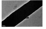
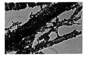
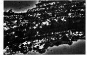
- a scanning electron microscope (SEM) photograph of the obtained film-like lead iodide / PVB nanofiber aggregate is shown in FIG.
- FIG. 1 a transmission electron microscope (TEM) photograph is shown in FIG.
- TEM transmission electron microscope
- Example 2 Production of fibrous aggregates of lead iodide crystals
- 2-propanol was added dropwise to the film-like lead iodide / PVB nanofiber assembly obtained in Example 1 so that the whole was wet, and dried on a hot plate at 70 ° C.
- the PVB was washed to obtain a fibrous aggregate of lead iodide crystals.
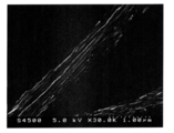
- FIG. 3 shows a fibrous aggregate SEM photograph of this lead iodide crystal
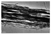
- FIG. 4 shows a TEM photograph
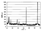
- FIG. 5 shows the result of X-ray crystal structure analysis (XRD). From the SEM image of FIG. 3 and the TEM image of FIG. 4, it can be seen that about 10 nm lead iodide nanofibers are assembled with the long axis of the crystal aligned.
- XRD X-ray crystal structure analysis
- Example 3 (Preparation of fibrous aggregate of perovskite compound crystal 1) Methylammonium iodide was vapor-deposited on the film-like lead iodide / PVB nanofiber aggregate obtained in Example 1. The distance between the target lead iodide / PVB nanofiber aggregate and methylammonium iodide was 6 cm, and 0.1 g of methylammonium iodide was heated to 150 ° C. under reduced pressure and reacted for 3 hours. To this, 2-propanol was added dropwise using a Pasteur pipette so as to be wet, and dried on a hot plate at 70 ° C.
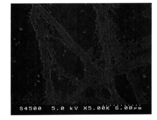
- FIG. 6 A fibrous aggregate SEM photograph of this perovskite compound crystal is shown in FIG. 6, a TEM photograph is shown in FIG. 7, and a result of XRD is shown in FIG. From the SEM image in FIG. 6 and the TEM image in FIG. 7, it can be seen that the crystallite size is 1 nm or more and 100 nm or less, and the crystallite contains a structure arranged in the fiber axis direction. Comparing the XRD result of lead iodide in FIG. 5 with FIG. 8, it can be seen that the peak indicating the lead iodide crystal completely disappeared and all changed to a perovskite compound crystal.
- Example 4 (Preparation of fibrous aggregates of perovskite compound crystals 2) Methylammonium iodide was vapor-deposited on the fibrous aggregate of film-like lead iodide crystals obtained in Example 2. The distance between the target lead iodide / PVB nanofiber aggregate and methylammonium iodide was 12 cm, and 0.1 g of methylammonium iodide was heated to 150 ° C. under reduced pressure and reacted for 8 hours.
- nanofiber-like lead iodide, perovskite compound crystals, or perovskite compound crystals having a uniform crystal size and one-dimensional arrangement.
Landscapes
- Engineering & Computer Science (AREA)
- Textile Engineering (AREA)
- Chemical & Material Sciences (AREA)
- Chemical Kinetics & Catalysis (AREA)
- General Chemical & Material Sciences (AREA)
- Organic Chemistry (AREA)
- Manufacturing & Machinery (AREA)
- Mechanical Engineering (AREA)
- Inorganic Fibers (AREA)
- Artificial Filaments (AREA)
- Nonwoven Fabrics (AREA)
Abstract
ペロブスカイト化合物の結晶サイズ及びその配置を規則正しく制御する技術を提供することを課題とする。 ナノファイバー状のヨウ化鉛などのハロゲン化金属、ペロブスカイト化合物結晶、もしくは結晶サイズが揃い一次元に配列したペロブスカイト化合物結晶及びそれらの繊維状集合体と膜状体を提供する。
Description
本発明は、ハロゲン化金属を含有するナノファイバー、ハロゲン化金属結晶、ハロゲン化金属結晶の繊維状集合体及び膜状体、ペロブスカイト化合物結晶の繊維状集合体及び膜状体に関し、光電変換装置に好適に用いられる材料の結晶構造制御に属し、特にヨウ化鉛系ペロブスカイト化合物を光電変換素子とする新規な光電変換装置用材料の結晶構造制御に関する。
近年、二酸化炭素による地球温暖化及び化石燃料の枯渇の懸念から、環境に対しよりクリーンな再生可能エネルギーが求められている。バイオマス由来の燃料は、既存の燃料から代替が可能であるが、生産のエネルギー及び製造コストが問題となっている。電気エネルギーに限定されるが、太陽光エネルギーは無尽蔵であり、安価なエネルギーとなりうるポテンシャルを秘めている。またシリコン結晶、シリコン薄膜、銅・インジウム・セレン接合(CIS型)などの無機材料を用いる物理接合型の太陽電池に対し、有機材料を発電層及び電荷輸送層に用いる有機系太陽電池は、分子設計によって特性のチューニングが可能であり、印刷によって製造コストを下げる事ができる可能性を秘めている。
有機アンモニウム分子層と金属ハライド層とが交互に積層した超格子構造を有するハライド系層状ペロブスカイト化合物は、従来から発光素子として利用できることが報告されている(特許文献1)。近年、金属ハライドとしてヨウ化鉛を採用したヨウ化鉛系層状ペロブスカイト化合物を太陽電池の光吸収層の材料として利用した例が報告されている(非特許文献1)。これは色素増感型太陽電池と有機薄膜型太陽電池の原理を融合した新しい材料であり、塗布で作製できる太陽電池として大変有望である。ペロブスカイト化合物の結晶成長とその構造は、光電子の伝達機構に影響する。ペロブスカイト化合物の前駆体であるヨウ化鉛のN-ジメチルホルムアミド溶媒中での結晶構造はあきらかになっているが(非特許文献2)、その構造及びペロブスカイト化合物の結晶構造を制御する方法は開発されていない。
Scientific Reports 2, Article number: 591, 2012
Chem. Lett. 2014, 43, 711-713
ペロブスカイト化合物を光吸収層の材料として用いる太陽電池の多くはコーティングによって作製され、結晶サイズ及びその配置を規則正しく制御する技術は確立されていない。そこで、本発明は、ナノファイバー状のヨウ化鉛などのハロゲン化金属、ペロブスカイト化合物結晶、もしくは結晶サイズが揃い一次元に配列したペロブスカイト化合物結晶及びそれらの繊維状集合体と膜状体を提供することを課題とする。
本発明者らは鋭意検討の結果、以下の手段により、課題を解決しうる発明をなした。
(1)一般式MX2(式中、Mは、2価の金属イオンであり、Xは、F,Cl,Br,Iのいずれかである。)で示されるハロゲン化金属を含有する繊維径1nm以上1μm以下のナノファイバー。
(2)一般式MX2で示されるハロゲン化金属結晶の2価の金属イオンMがPbである(1)に記載のナノファイバー。
(3)一般式MX2で示されるハロゲン化金属が繊維軸方向に配向している(1)または(2)に記載のナノファイバー。
(4)アスペクト比が1以上の一般式MX2(式中、Mは、2価の金属イオンであり、Xは、F,Cl,Br,Iのいずれかである。)で示されるハロゲン化金属結晶。
(5)一般式MX2で示されるハロゲン化金属結晶の2価の金属イオンMがPbである(4)に記載のハロゲン化金属結晶。
(6)(4)または(5)に記載の一般式MX2で示されるハロゲン化金属結晶がその結晶の長軸を揃えて集合したハロゲン化金属結晶の繊維状集合体。
(7)(6)に記載の一般式MX2で示されるハロゲン化金属結晶の繊維状集合体よりなる膜状体。
(8)結晶子のサイズが1nm以上100nm以下であり、結晶子が繊維軸方向に配列した構造を含有する一般式CH3NH3MX3(式中、Mは、2価の金属イオンであり、Xは、F,Cl,Br,Iのいずれかである。)で示されるペロブスカイト化合物結晶の繊維状集合体。
(9)一般式CH3NH3MX3で示されるペロブスカイト化合物結晶の2価の金属イオンMがPbである(8)に記載のペロブスカイト化合物結晶の繊維状集合体。
(10)(8)または(9)に記載の一般式CH3NH3MX3で示されるペロブスカイト化合物結晶の繊維状集合体よりなる膜状体。
(11)一般式MX2(式中、Mは、2価の金属イオンであり、Xは、F,Cl,Br,Iのいずれかである。)で示されるハロゲン化金属を含有する高分子溶液を荷電紡糸する事によって(1)~(3)のいずれかに記載のナノファイバーを得る工程を含む、ハロゲン化金属含有ナノファイバーの製造方法。
(12)(11)の高分子溶液に用いる高分子がポリビニルブチラールであるハロゲン化金属含有ナノファイバーの製造方法。
(13)(11)または(12)に記載の製造方法で得られたハロゲン化金属含有ナノファイバーの高分子を、ハロゲン化金属を溶かさず高分子を溶かす溶媒を用いて除去し、(4)または(5)に記載のハロゲン化金属結晶を得る工程を含む、ハロゲン化金属結晶の製造方法。
(14)(13)に記載の製造方法で得られたハロゲン化金属結晶を繊維状集合体として、(6)に記載のハロゲン化金属結晶の繊維状集合体を得る工程を含む、ハロゲン化金属結晶の繊維状集合体の製造方法。
(15)(14)に記載の製造方法で得られたハロゲン化金属結晶の繊維状集合体を膜状体として、(7)に記載の膜状体を得る工程を含む、ハロゲン化金属結晶の繊維状集合体よりなる膜状体の製造方法。
(16)(11)または(12)に記載のハロゲン化金属含有ナノファイバーの製造方法により得られたハロゲン化金属含有ナノファイバーを一般式CH3NH3X(式中、Xは、F,Cl,Br,Iのいずれかである。)の蒸気で処理する事により一般式CH3NH3MX3(式中、Mは、2価の金属イオンであり、Xは、F,Cl,Br,Iのいずれかである。)で示されるペロブスカイト化合物結晶を生成させ、ペロブスカイト化合物結晶を溶かさず高分子を溶かす溶媒を用いて除去し、(8)または(9)に記載のペロブスカイト化合物結晶の繊維状集合体を得る工程を含む、ペロブスカイト化合物結晶の繊維状集合体の製造方法。
(17)(16)に記載の製造方法で得られたペロブスカイト化合物結晶の繊維状集合体を膜状体として、(10)に記載のペロブスカイト化合物結晶の繊維状集合体よりなる膜状体を得る工程を含む、ペロブスカイト化合物結晶の繊維状集合体よりなる膜状体の製造方法。
(18)(6)の一般式MX2で示されるハロゲン化金属結晶の繊維状集合体を一般式CH3NH3Xの蒸気(式中、Xは、F,Cl,Br,Iのいずれかである。)で処理する事により一般式CH3NH3MX3(式中、Mは、2価の金属イオンであり、Xは、F,Cl,Br,Iのいずれかである。)で示されるペロブスカイト化合物結晶を生成させ、(8)または(9)に記載のペロブスカイト化合物結晶の繊維状集合体を得る工程を含む、ペロブスカイト化合物結晶の繊維状集合体の製造方法。
(19)(7)に記載の一般式MX2で示されるハロゲン化金属結晶の繊維状集合体よりなる膜状体を一般式CH3NH3Xの蒸気(式中、Xは、F,Cl,Br,Iのいずれかである。)で処理する事により一般式CH3NH3MX3(式中、Mは、2価の金属イオンであり、Xは、F,Cl,Br,Iのいずれかである。)で示されるペロブスカイト化合物結晶を生成させ、(10)に記載のペロブスカイト化合物結晶の繊維状集合体よりなる膜状体を得る工程を含む、ペロブスカイト化合物結晶の繊維状集合体よりなる膜状体の製造方法。
(2)一般式MX2で示されるハロゲン化金属結晶の2価の金属イオンMがPbである(1)に記載のナノファイバー。
(3)一般式MX2で示されるハロゲン化金属が繊維軸方向に配向している(1)または(2)に記載のナノファイバー。
(4)アスペクト比が1以上の一般式MX2(式中、Mは、2価の金属イオンであり、Xは、F,Cl,Br,Iのいずれかである。)で示されるハロゲン化金属結晶。
(5)一般式MX2で示されるハロゲン化金属結晶の2価の金属イオンMがPbである(4)に記載のハロゲン化金属結晶。
(6)(4)または(5)に記載の一般式MX2で示されるハロゲン化金属結晶がその結晶の長軸を揃えて集合したハロゲン化金属結晶の繊維状集合体。
(7)(6)に記載の一般式MX2で示されるハロゲン化金属結晶の繊維状集合体よりなる膜状体。
(8)結晶子のサイズが1nm以上100nm以下であり、結晶子が繊維軸方向に配列した構造を含有する一般式CH3NH3MX3(式中、Mは、2価の金属イオンであり、Xは、F,Cl,Br,Iのいずれかである。)で示されるペロブスカイト化合物結晶の繊維状集合体。
(9)一般式CH3NH3MX3で示されるペロブスカイト化合物結晶の2価の金属イオンMがPbである(8)に記載のペロブスカイト化合物結晶の繊維状集合体。
(10)(8)または(9)に記載の一般式CH3NH3MX3で示されるペロブスカイト化合物結晶の繊維状集合体よりなる膜状体。
(11)一般式MX2(式中、Mは、2価の金属イオンであり、Xは、F,Cl,Br,Iのいずれかである。)で示されるハロゲン化金属を含有する高分子溶液を荷電紡糸する事によって(1)~(3)のいずれかに記載のナノファイバーを得る工程を含む、ハロゲン化金属含有ナノファイバーの製造方法。
(12)(11)の高分子溶液に用いる高分子がポリビニルブチラールであるハロゲン化金属含有ナノファイバーの製造方法。
(13)(11)または(12)に記載の製造方法で得られたハロゲン化金属含有ナノファイバーの高分子を、ハロゲン化金属を溶かさず高分子を溶かす溶媒を用いて除去し、(4)または(5)に記載のハロゲン化金属結晶を得る工程を含む、ハロゲン化金属結晶の製造方法。
(14)(13)に記載の製造方法で得られたハロゲン化金属結晶を繊維状集合体として、(6)に記載のハロゲン化金属結晶の繊維状集合体を得る工程を含む、ハロゲン化金属結晶の繊維状集合体の製造方法。
(15)(14)に記載の製造方法で得られたハロゲン化金属結晶の繊維状集合体を膜状体として、(7)に記載の膜状体を得る工程を含む、ハロゲン化金属結晶の繊維状集合体よりなる膜状体の製造方法。
(16)(11)または(12)に記載のハロゲン化金属含有ナノファイバーの製造方法により得られたハロゲン化金属含有ナノファイバーを一般式CH3NH3X(式中、Xは、F,Cl,Br,Iのいずれかである。)の蒸気で処理する事により一般式CH3NH3MX3(式中、Mは、2価の金属イオンであり、Xは、F,Cl,Br,Iのいずれかである。)で示されるペロブスカイト化合物結晶を生成させ、ペロブスカイト化合物結晶を溶かさず高分子を溶かす溶媒を用いて除去し、(8)または(9)に記載のペロブスカイト化合物結晶の繊維状集合体を得る工程を含む、ペロブスカイト化合物結晶の繊維状集合体の製造方法。
(17)(16)に記載の製造方法で得られたペロブスカイト化合物結晶の繊維状集合体を膜状体として、(10)に記載のペロブスカイト化合物結晶の繊維状集合体よりなる膜状体を得る工程を含む、ペロブスカイト化合物結晶の繊維状集合体よりなる膜状体の製造方法。
(18)(6)の一般式MX2で示されるハロゲン化金属結晶の繊維状集合体を一般式CH3NH3Xの蒸気(式中、Xは、F,Cl,Br,Iのいずれかである。)で処理する事により一般式CH3NH3MX3(式中、Mは、2価の金属イオンであり、Xは、F,Cl,Br,Iのいずれかである。)で示されるペロブスカイト化合物結晶を生成させ、(8)または(9)に記載のペロブスカイト化合物結晶の繊維状集合体を得る工程を含む、ペロブスカイト化合物結晶の繊維状集合体の製造方法。
(19)(7)に記載の一般式MX2で示されるハロゲン化金属結晶の繊維状集合体よりなる膜状体を一般式CH3NH3Xの蒸気(式中、Xは、F,Cl,Br,Iのいずれかである。)で処理する事により一般式CH3NH3MX3(式中、Mは、2価の金属イオンであり、Xは、F,Cl,Br,Iのいずれかである。)で示されるペロブスカイト化合物結晶を生成させ、(10)に記載のペロブスカイト化合物結晶の繊維状集合体よりなる膜状体を得る工程を含む、ペロブスカイト化合物結晶の繊維状集合体よりなる膜状体の製造方法。
本発明によれば、ナノファイバー状のヨウ化鉛などのハロゲン化金属、ペロブスカイト化合物結晶、もしくは結晶サイズが揃い一次元に配列したペロブスカイト化合物結晶及びそれらの繊維状集合体と膜状体を提供する事ができる。
本発明で用いられるハロゲン化金属は、一般式MX2で示される。式中、Mは、2価の金属イオンである。これらの2価の金属イオンは、Sn及びPbであることが好ましく、Pbであることがさらに好ましい。Xは、F,Cl,Br,Iいずれかのハロゲンである。これらのハロゲンは、Cl,Br,Iであることが好ましく、Iであることがさらに好ましい。
本発明のナノファイバーは、前記のハロゲン化金属を含有するナノファイバーである。ナノファイバーの繊維径は1nm以上1μm以下であり、より好ましくは500nm以下である。該ナノファイバーにおいて、ハロゲン化金属は結晶状態でナノファイバーの繊維軸方向に配向していることが好ましい。配向の有無及びその状態は、走査型電子顕微鏡(SEM)あるいは透過型電子顕微鏡(TEM)での形態観察により確認が可能であり、結晶状態はX線結晶構造解析(XRD)で確認することが可能である。
ハロゲン化金属はペロブスカイト化合物結晶の前駆体であり、ハロゲン化金属をナノファイバー状にすることでペロブスカイト化合物結晶の構造を制御する。
ハロゲン化金属はペロブスカイト化合物結晶の前駆体であり、ハロゲン化金属をナノファイバー状にすることでペロブスカイト化合物結晶の構造を制御する。
本発明においては、アスペクト比が1以上の前記一般式MX2で示されるハロゲン化金属結晶であることも発明の一様態である。該ハロゲン化金属結晶は、後述の製造方法によりその結晶の長軸を揃えて集合したハロゲン化金属結晶の繊維状集合体とすることができ、該繊維状集合体よりなる膜状体とすることもできる。ペロブスカイト化合物を用いた太陽電池は、印刷によって作製できる事が特徴の一つである。ペロブスカイト化合物の前駆体であるハロゲン化金属結晶を繊維状集合体、膜状体にすることにより、産業化した場合に、印刷によって作製でき、工程に応じて蒸着法及び溶液法でのペロブスカイト化合物結晶の製法を選択できる。
本発明の好ましい様態は、結晶子のサイズが1nm以上100nm以下であり、結晶子が繊維軸方向に配列した構造を含有する一般式CH3NH3MX3(式中、Mは、2価の金属イオンであり、Xは、F,Cl,Br,Iのいずれかである。)で示されるペロブスカイト化合物結晶の繊維状集合体である。該一般式CH3NH3MX3における金属イオンMは、Pbであることが好ましく、該繊維状集合体よりなる膜状体とすることもできる。
本発明のハロゲン化金属含有ナノファイバーの製造方法は、ハロゲン化金属を含有する高分子溶液を紡糸する製造方法である。ハロゲン化金属を含有する高分子溶液を紡糸する方法には、エレクトロスピニング法、セルフアセンブリ法、フェイズセパレーション法などが挙げられるが、多種類のポリマーに使用できる点、及び、ナノレベルでのファイバー形状の調節も容易な点でエレクトロスピニング法が好ましい。
本発明の製造方法において採用されるエレクトロスピニング法とは、曳糸性高分子溶液に高電圧を印加することによって、該溶液をスプレーし、ナノファイバーを形成させる方法である。
エレクトロスピニングのための装置としては、従来の知見から各種の様々な装置が知られているが、基本的には、曳糸性高分子溶液を供給するシリンジ及びシリンジポンプなどの手段と、供給される曳糸性高分子溶液をスプレーする単一又は複数のニードル部と、形成したナノファイバーを捕集するコレクター部、及び前記のニードル部とコレクター部との間に高電圧を印加する高電圧発生手段を備えた装置が用いられる。電圧としては、通常10~30kV程度印加される。これにより、コレクターに静電引力が発生し、静電引力が曳糸性高分子溶液の表面張力を上回ったとき、高分子溶液がニードル部よりスプレーされる。スプレーされた高分子溶液は、コレクターに到達するまでに溶媒が揮発除去され、ナノファイバーとなって、コレクター上に吸い寄せられる。
さらに、近年では、エレクトロスピニング法として、量産化のために、シリンジポンプを複数本並べて、ナノファイバーを作製する方法や、ニードルタイプのシリンジポンプを用いるのではなく、ロールタイプやフラットノズルタイプの方法も開発されており、本発明においては、これら方法も採用することが可能である。
本発明の製造方法において採用されるエレクトロスピニング法とは、曳糸性高分子溶液に高電圧を印加することによって、該溶液をスプレーし、ナノファイバーを形成させる方法である。
エレクトロスピニングのための装置としては、従来の知見から各種の様々な装置が知られているが、基本的には、曳糸性高分子溶液を供給するシリンジ及びシリンジポンプなどの手段と、供給される曳糸性高分子溶液をスプレーする単一又は複数のニードル部と、形成したナノファイバーを捕集するコレクター部、及び前記のニードル部とコレクター部との間に高電圧を印加する高電圧発生手段を備えた装置が用いられる。電圧としては、通常10~30kV程度印加される。これにより、コレクターに静電引力が発生し、静電引力が曳糸性高分子溶液の表面張力を上回ったとき、高分子溶液がニードル部よりスプレーされる。スプレーされた高分子溶液は、コレクターに到達するまでに溶媒が揮発除去され、ナノファイバーとなって、コレクター上に吸い寄せられる。
さらに、近年では、エレクトロスピニング法として、量産化のために、シリンジポンプを複数本並べて、ナノファイバーを作製する方法や、ニードルタイプのシリンジポンプを用いるのではなく、ロールタイプやフラットノズルタイプの方法も開発されており、本発明においては、これら方法も採用することが可能である。
エレクトロスピニング法においては、曳糸性有機物質溶液が用いられる。曳糸性有機物質としては、溶液状態で曳糸性を有する有機物質であればよく、特に制限されず、有機高分子及び有機低分子化合物のいずれも用いることができるが、得られる繊維状物の物性や用途などを考慮すると、前述したように、有機高分子が好適である。
この有機高分子としては、溶液状態で曳糸性を有し、含有するハロゲン化金属が溶解するのであれば、有機溶媒可溶性のもの及び水系媒体可溶性のもの、いずれも用いることができる。
この有機高分子としては、溶液状態で曳糸性を有し、含有するハロゲン化金属が溶解するのであれば、有機溶媒可溶性のもの及び水系媒体可溶性のもの、いずれも用いることができる。
有機溶媒可溶性の曳糸性高分子としては、例えばポリアミド6、ポリアミド46、ポリアミド66、ポリアミド610、ポリアミド612、ポリアミド11、ポリアミド12、ポリアミド6/66共重合体、及び芳香族ポリアミドなどのポリアミド類;ポリエチレンテレフタレート、ポリブチレンテレフタレート、ポリエチレン2,6-ナフタレートなどのポリエステル類;ポリプロピレン及びポリエチレンなどのポリオレフィン類;ポリ塩化ビニル及び塩化ビニル/塩化ビニリデン共重合体などの塩素化オレフィン重合体類;ポリウレタン類、及びポリアクリロニトリルなどを挙げることができる。これらは1種を単独で用いてもよく、2種以上を組み合わせて用いてもよい。
一方、水系媒体可溶性の曳糸性有機高分子としては、例えばポリビニルアルコール、ポリエチレングリコール、ポリプロピレングリコールなどを挙げることができる。これらは1種を単独で用いてもよく、2種以上を組み合わせて用いてもよい。
一方、水系媒体可溶性の曳糸性有機高分子としては、例えばポリビニルアルコール、ポリエチレングリコール、ポリプロピレングリコールなどを挙げることができる。これらは1種を単独で用いてもよく、2種以上を組み合わせて用いてもよい。
前記有機溶媒可溶性の曳糸性高分子を溶解して、その溶液を調製するのに用いる有機溶媒としては、上記高分子を溶解することができ、含有するハロゲン化金属が溶解し、かつエレクトロスピニング時において、ニードル部からスプレーされた、高分子溶液が、コレクターに到達するまでに、揮発除去し得るものであれば特に制限されず、各種の有機溶媒が用いられる。
一方、前記水系媒体可溶性の曳糸性高分子を溶解して、その溶液を調製するのに用いる水系媒体としては、水の他、水と低級アルコール、あるいは水とアセトンのような低級ケトンとの混合溶媒などを用いることができる。
一方、前記水系媒体可溶性の曳糸性高分子を溶解して、その溶液を調製するのに用いる水系媒体としては、水の他、水と低級アルコール、あるいは水とアセトンのような低級ケトンとの混合溶媒などを用いることができる。
太陽電池光吸収層のペロブスカイト化合物結晶前駆体としてハロゲン化金属含有ナノファイバーを作製するのであれば、含水率を極力減らす事が好ましく、その曳糸性高分子は、有機溶媒可溶性の曳糸性高分子を用いる事が好ましい。一般式MX2で示されるハロゲン化金属結晶の2価の金属イオンMがPbであるハロゲン化金属結晶を得る場合、曳糸性高分子にはポリビニルブチラール、ポリビニルピロリドン、ポリスチレン、ポリメタクリル酸メチル、ポリアクリロニトリルなどを用いることが好ましく、ポリビニルブチラールであることがさらに好ましい。有機溶媒としては、ジメチルホルムアミド、ジメチルスルホキシド、ジメチルアセトアミド、N-メチル-2-ピロリドンなどを用いることが好ましい。
曳糸性高分子溶液の濃度は、溶媒と有機物質との組み合わせによって左右されるが、所望の径を有する有機ナノファイバーを形成する観点から、通常5~30質量%程度、好ましくは7~20質量%である。該濃度が5質量%未満では、ファイバーが得られずに、粒状物が形成するおそれがあり、一方30質量%を超えると、ファイバーの径が太くなりすぎてナノファイバーが形成されないおそれが生じる。形成されるナノファイバーの平均直径は、通常1nm以上1μm以下程度である。
エレクトロスピニング法により、コレクター上に形成されるナノファイバーは、通常膜状などのナノファイバーの集合体形状に形成される。
エレクトロスピニング法により、コレクター上に形成されるナノファイバーは、通常膜状などのナノファイバーの集合体形状に形成される。
曳糸性高分子溶液中のハロゲン化金属濃度は、溶媒と曳糸性高分子との組み合わせによって左右されるが、ナノファイバー状のハロゲン化金属結晶を得る観点から、飽和濃度とする事が好ましい。
一般式MX2で示されるナノファイバー状のハロゲン化金属結晶の製造方法は、上記ハロゲン化金属含有ナノファイバーの製造方法により得られたハロゲン化金属含有ナノファイバーを、ハロゲン化金属を溶かさず高分子を溶かす溶媒を用いて除去し、ハロゲン化金属結晶を得る製造方法である。
用いる溶媒に特に制限はないが、高分子にポリビニルブチラールを用いる場合は、2-プロパノールを用いるのが好ましい。
用いる溶媒に特に制限はないが、高分子にポリビニルブチラールを用いる場合は、2-プロパノールを用いるのが好ましい。
ペロブスカイト化合物結晶の製造方法は、二通りの方法が可能である。
一般式MX2で示されるハロゲン化金属含有ナノファイバーの製造方法により得られたハロゲン化金属含有ナノファイバーを一般式CH3NH3X(式中、Xは、F,Cl,Br,Iのいずれかである。)の蒸気もしくは溶液で処理する事により一般式CH3NH3MX3(式中、Mは、2価の金属イオンであり、Xは、F,Cl,Br,Iのいずれかである。)で示されるペロブスカイト化合物結晶を生成させ、ペロブスカイト化合物結晶を溶かさず高分子を溶かす溶媒を用いて除去し、ペロブスカイト化合物結晶を得る方法。
一般式MX2で示されるハロゲン化金属結晶を一般式CH3NH3X(式中、Xは、F,Cl,Br,Iのいずれかである。)の蒸気もしくは溶液で処理する事により一般式CH3NH3MX3(式中、Mは、2価の金属イオンであり、Xは、F,Cl,Br,Iのいずれかである。)で示されるペロブスカイト化合物結晶を生成させる方法。
一般式MX2で示されるハロゲン化金属含有ナノファイバーの製造方法により得られたハロゲン化金属含有ナノファイバーを一般式CH3NH3X(式中、Xは、F,Cl,Br,Iのいずれかである。)の蒸気もしくは溶液で処理する事により一般式CH3NH3MX3(式中、Mは、2価の金属イオンであり、Xは、F,Cl,Br,Iのいずれかである。)で示されるペロブスカイト化合物結晶を生成させ、ペロブスカイト化合物結晶を溶かさず高分子を溶かす溶媒を用いて除去し、ペロブスカイト化合物結晶を得る方法。
一般式MX2で示されるハロゲン化金属結晶を一般式CH3NH3X(式中、Xは、F,Cl,Br,Iのいずれかである。)の蒸気もしくは溶液で処理する事により一般式CH3NH3MX3(式中、Mは、2価の金属イオンであり、Xは、F,Cl,Br,Iのいずれかである。)で示されるペロブスカイト化合物結晶を生成させる方法。
一般式MX2で示されるハロゲン化金属含有ナノファイバーもしくは、ハロゲン化金属結晶を一般式CH3NH3Xの蒸気もしくは溶液で処理する方法は、例えば下記のようにして実施する事ができる。
まず蒸気で処理する場合、200℃以下、好ましくは150℃のホットプレート上に一般式CH3NH3X源を置き、ハロゲン化金属含有ナノファイバーもしくは、ハロゲン化金属結晶をホットプレート上15cm以下好ましくは6cmの距離に設置する。全体を覆い、大気圧下もしくは減圧下で蒸着処理を行う。ペロブスカイト化合物結晶を溶かさず一般式CH3NH3Xを溶かす溶媒、好ましくは2-プロパノールを用いて洗浄し、乾燥する。
溶液で処理する場合、ペロブスカイト化合物結晶を溶かさず一般式CH3NH3Xを溶かす溶媒に一般式CH3NH3Xを溶かし、ハロゲン化金属含有ナノファイバーもしくは、ハロゲン化金属結晶を浸漬させる。ペロブスカイト化合物結晶を溶かさず一般式CH3NH3Xを溶かす溶媒、好ましくは2-プロパノールを用いて洗浄し、乾燥する。
配列した結晶を得る観点から蒸気で処理する方法が好ましい。一般式CH3NH3XのXは、F,Cl,Br,Iいずれかのハロゲンであるが、必ずしも処理をする一般式MX2で示されるハロゲン化金属のハロゲンXと一致している必要はない。これらのハロゲンは、Cl,Br,Iであることが好ましく、Iであることがさらに好ましい。
まず蒸気で処理する場合、200℃以下、好ましくは150℃のホットプレート上に一般式CH3NH3X源を置き、ハロゲン化金属含有ナノファイバーもしくは、ハロゲン化金属結晶をホットプレート上15cm以下好ましくは6cmの距離に設置する。全体を覆い、大気圧下もしくは減圧下で蒸着処理を行う。ペロブスカイト化合物結晶を溶かさず一般式CH3NH3Xを溶かす溶媒、好ましくは2-プロパノールを用いて洗浄し、乾燥する。
溶液で処理する場合、ペロブスカイト化合物結晶を溶かさず一般式CH3NH3Xを溶かす溶媒に一般式CH3NH3Xを溶かし、ハロゲン化金属含有ナノファイバーもしくは、ハロゲン化金属結晶を浸漬させる。ペロブスカイト化合物結晶を溶かさず一般式CH3NH3Xを溶かす溶媒、好ましくは2-プロパノールを用いて洗浄し、乾燥する。
配列した結晶を得る観点から蒸気で処理する方法が好ましい。一般式CH3NH3XのXは、F,Cl,Br,Iいずれかのハロゲンであるが、必ずしも処理をする一般式MX2で示されるハロゲン化金属のハロゲンXと一致している必要はない。これらのハロゲンは、Cl,Br,Iであることが好ましく、Iであることがさらに好ましい。
本願は、2015年4月13日に出願された日本国特許出願第2015-081661号に基づく優先権の利益を主張するものである。2015年4月13日に出願された日本国特許出願第2015-081661号の明細書の全内容が、本願に参考のため援用される。
以下、本発明について実施例を用いて具体的に説明するが、本発明はこれらの実施例に限定されることはない。
(走査型電子顕微鏡観察)
走査型電子顕微鏡(SEM)の試料作製及び観察は下記のように実施した。アルミ箔基材上に作製したナノファイバーをアルミ基材ごとSEM台に導電性両面テープで張り付け、薄くPtコーティングを施してSEM観察用試料とした。SEMは日立ハイテクノロジーズ社製S-4500を加速電圧5.0kVにて使用した。観察は、5,000~30,000倍程度の拡大倍率にて実施した。
走査型電子顕微鏡(SEM)の試料作製及び観察は下記のように実施した。アルミ箔基材上に作製したナノファイバーをアルミ基材ごとSEM台に導電性両面テープで張り付け、薄くPtコーティングを施してSEM観察用試料とした。SEMは日立ハイテクノロジーズ社製S-4500を加速電圧5.0kVにて使用した。観察は、5,000~30,000倍程度の拡大倍率にて実施した。
(透過型電子顕微鏡観察)
透過型電子顕微鏡(TEM)の試料作製及び観察は下記のように実施した。カーボン膜を貼った銅300メッシュの上にナノファイバーを作製し、洗浄及びペロブスカイト結晶化などの必要な処理を施した後に、薄くカーボン蒸着を施してTEM観察用試料とした。
TEMは日本電子社製JEM-2100を加速電圧200kVにて使用した。観察は、10,000~100,000倍程度の拡大倍率にて実施し、Gatan社製CCDカメラ(SC1000Model832)にて画像を撮影し、記録した。
透過型電子顕微鏡(TEM)の試料作製及び観察は下記のように実施した。カーボン膜を貼った銅300メッシュの上にナノファイバーを作製し、洗浄及びペロブスカイト結晶化などの必要な処理を施した後に、薄くカーボン蒸着を施してTEM観察用試料とした。
TEMは日本電子社製JEM-2100を加速電圧200kVにて使用した。観察は、10,000~100,000倍程度の拡大倍率にて実施し、Gatan社製CCDカメラ(SC1000Model832)にて画像を撮影し、記録した。
(X線構造解析)
ナノファイバーはアルミ箔基材上に作製しており、ハロゲン化金属結晶及びペロブスカイト化合物結晶の回折ピークを測定する場合、基材からの回折が強いため集中法光学系では精密に測定することが困難となることが多い。そこで試料表面に対してX線をごく浅い角度で入射し侵入深さを制限することにより基材の影響を出来るだけ抑えた薄膜法を用いることが望ましい。
X線回折装置はRigaku製 薄膜評価用試料水平型X線回折装置SmartLabを用いて測定した。多層膜ミラーを用いた平行ビーム光学系を用い、光源にはCuKα線(波長:1.54186Å)を40kV、30mAの出力で用いた。入射側スリット系はソーラスリット5.0°、入射スリット0.2mm,長手制御スリット10mmを用い、受光側スリットにはパラレルスリットアナライザー(PSA)0.114degを用いた。試料はステージに両面テープで固定するか、または多孔質吸着試料ホルダを用いて吸着固定してもよい。X線の入射角1.0°とし、アウトオブプレーン方向にシンチレーションカウンター検出器を走査し,ステップ間隔0.02°、測定スピード2.0°/minで測定した。
ナノファイバーはアルミ箔基材上に作製しており、ハロゲン化金属結晶及びペロブスカイト化合物結晶の回折ピークを測定する場合、基材からの回折が強いため集中法光学系では精密に測定することが困難となることが多い。そこで試料表面に対してX線をごく浅い角度で入射し侵入深さを制限することにより基材の影響を出来るだけ抑えた薄膜法を用いることが望ましい。
X線回折装置はRigaku製 薄膜評価用試料水平型X線回折装置SmartLabを用いて測定した。多層膜ミラーを用いた平行ビーム光学系を用い、光源にはCuKα線(波長:1.54186Å)を40kV、30mAの出力で用いた。入射側スリット系はソーラスリット5.0°、入射スリット0.2mm,長手制御スリット10mmを用い、受光側スリットにはパラレルスリットアナライザー(PSA)0.114degを用いた。試料はステージに両面テープで固定するか、または多孔質吸着試料ホルダを用いて吸着固定してもよい。X線の入射角1.0°とし、アウトオブプレーン方向にシンチレーションカウンター検出器を走査し,ステップ間隔0.02°、測定スピード2.0°/minで測定した。
(ヨウ化メチルアンモニウムの作製)
氷上に置いた40%メチルアミンメタノール溶液13.93mLに、55%ヨウ化水素酸水溶液15mLを加え、氷上のまま4時間攪拌した。これを55℃でエバポレートし、減圧下55℃で10分乾燥させた。得られた粉体をエタノール100mLに溶解し、ジエチルエーテル300mLに再沈殿させた。濾過後60℃で24時間真空乾燥した。
氷上に置いた40%メチルアミンメタノール溶液13.93mLに、55%ヨウ化水素酸水溶液15mLを加え、氷上のまま4時間攪拌した。これを55℃でエバポレートし、減圧下55℃で10分乾燥させた。得られた粉体をエタノール100mLに溶解し、ジエチルエーテル300mLに再沈殿させた。濾過後60℃で24時間真空乾燥した。
(実施例1)
(ヨウ化鉛含有ナノファイバーの作製)
ヨウ化鉛5.25gをN-ジメチルホルムアミド(DMF)13mLに溶解して、ホットスターラー上100℃で30分攪拌し、70℃で保温した。このヨウ化鉛-DMF溶液3mLに、ポリビニルブチラール(PVB)[(株)クラレ製 モビタールB60T]0.3gを加え、ホットスターラー上70℃で攪拌、保温した。この溶液を横口シリンジに注入した。シリンジポンプ、ニードル部、コレクター部が水平方向に設置されたエレクトロスピニングを用い、横口シリンジのノズルを上向きに設置した。ラバーヒーターを用いて70℃に温めた陽極(シリンジ)へ15kVの電圧を印加し、陰極(コレクター部)へヨウ化鉛/PVBナノファイバーを堆積させて、ヨウ化鉛/PVBナノファイバー集合体を得た。紡糸時間は15分であり、また陰極にはアルミ箔を用いた。
得られた膜状のヨウ化鉛/PVBナノファイバー集合体の走査型電子顕微鏡(SEM)写真を図1に、透過型電子顕微鏡(TEM)の写真を図2に示す。約300nmヨウ化鉛含有PVBナノファイバー得られ、図2のTEM画像からPVB内でヨウ化鉛が繊維軸方向に配向していることがわかる。
(ヨウ化鉛含有ナノファイバーの作製)
ヨウ化鉛5.25gをN-ジメチルホルムアミド(DMF)13mLに溶解して、ホットスターラー上100℃で30分攪拌し、70℃で保温した。このヨウ化鉛-DMF溶液3mLに、ポリビニルブチラール(PVB)[(株)クラレ製 モビタールB60T]0.3gを加え、ホットスターラー上70℃で攪拌、保温した。この溶液を横口シリンジに注入した。シリンジポンプ、ニードル部、コレクター部が水平方向に設置されたエレクトロスピニングを用い、横口シリンジのノズルを上向きに設置した。ラバーヒーターを用いて70℃に温めた陽極(シリンジ)へ15kVの電圧を印加し、陰極(コレクター部)へヨウ化鉛/PVBナノファイバーを堆積させて、ヨウ化鉛/PVBナノファイバー集合体を得た。紡糸時間は15分であり、また陰極にはアルミ箔を用いた。
得られた膜状のヨウ化鉛/PVBナノファイバー集合体の走査型電子顕微鏡(SEM)写真を図1に、透過型電子顕微鏡(TEM)の写真を図2に示す。約300nmヨウ化鉛含有PVBナノファイバー得られ、図2のTEM画像からPVB内でヨウ化鉛が繊維軸方向に配向していることがわかる。
(実施例2)
(ヨウ化鉛結晶の繊維状集合体作製)
実施例1で得られた膜状のヨウ化鉛/PVBナノファイバー集合体に、パスツールピペットを用いて、2-プロパノールを全体が濡れるように滴下し、70℃のホットプレートで乾燥した。これを3回繰り返すことで、PVBを洗浄し、ヨウ化鉛結晶の繊維状集合体を得た。このヨウ化鉛結晶の繊維状集合体SEM写真を図3に、TEM写真を図4に、X線結晶構造解析(XRD)の結果を図5に示す。図3のSEM画像、図4のTEM画像から、約10nmヨウ化鉛ナノファイバーが結晶の長軸を揃えて集合していることがわかる。
(ヨウ化鉛結晶の繊維状集合体作製)
実施例1で得られた膜状のヨウ化鉛/PVBナノファイバー集合体に、パスツールピペットを用いて、2-プロパノールを全体が濡れるように滴下し、70℃のホットプレートで乾燥した。これを3回繰り返すことで、PVBを洗浄し、ヨウ化鉛結晶の繊維状集合体を得た。このヨウ化鉛結晶の繊維状集合体SEM写真を図3に、TEM写真を図4に、X線結晶構造解析(XRD)の結果を図5に示す。図3のSEM画像、図4のTEM画像から、約10nmヨウ化鉛ナノファイバーが結晶の長軸を揃えて集合していることがわかる。
(実施例3)
(ペロブスカイト化合物結晶の繊維状集合体作製1)
実施例1で得られた膜状のヨウ化鉛/PVBナノファイバー集合体に、ヨウ化メチルアンモニウムを蒸着させた。ターゲットであるヨウ化鉛/PVBナノファイバー集合体とヨウ化メチルアンモニウムの距離を6cmにし、減圧下でヨウ化メチルアンモニウム0.1gを150℃に加熱し3時間反応させた。これに、パスツールピペットを用いて、2-プロパノールを全体が濡れるように滴下し、70℃のホットプレートで乾燥した。これを3回繰り返すことで、PVBを洗浄し、ペロブスカイト化合物結晶の繊維状集合体を得た。このペロブスカイト化合物結晶の繊維状集合体SEM写真を図6に、TEM写真を図7に、XRDの結果を図8に示す。図6のSEM画像、図7のTEM画像から、結晶子のサイズが1nm以上100nm以下であり、結晶子が繊維軸方向に配列した構造を含有することがわかる。先の図5のヨウ化鉛のXRDの結果と図8を比較する事で、ヨウ化鉛の結晶を示すピークが完全に消え、すべてペロブスカイト化合物結晶に変化していることがわかる。
(ペロブスカイト化合物結晶の繊維状集合体作製1)
実施例1で得られた膜状のヨウ化鉛/PVBナノファイバー集合体に、ヨウ化メチルアンモニウムを蒸着させた。ターゲットであるヨウ化鉛/PVBナノファイバー集合体とヨウ化メチルアンモニウムの距離を6cmにし、減圧下でヨウ化メチルアンモニウム0.1gを150℃に加熱し3時間反応させた。これに、パスツールピペットを用いて、2-プロパノールを全体が濡れるように滴下し、70℃のホットプレートで乾燥した。これを3回繰り返すことで、PVBを洗浄し、ペロブスカイト化合物結晶の繊維状集合体を得た。このペロブスカイト化合物結晶の繊維状集合体SEM写真を図6に、TEM写真を図7に、XRDの結果を図8に示す。図6のSEM画像、図7のTEM画像から、結晶子のサイズが1nm以上100nm以下であり、結晶子が繊維軸方向に配列した構造を含有することがわかる。先の図5のヨウ化鉛のXRDの結果と図8を比較する事で、ヨウ化鉛の結晶を示すピークが完全に消え、すべてペロブスカイト化合物結晶に変化していることがわかる。
(実施例4)
(ペロブスカイト化合物結晶の繊維状集合体作製2)
実施例2で得られた膜状のヨウ化鉛結晶の繊維状集合体に、ヨウ化メチルアンモニウムを蒸着させた。ターゲットであるヨウ化鉛/PVBナノファイバー集合体とヨウ化メチルアンモニウムの距離を12cmにし、減圧下でヨウ化メチルアンモニウム0.1gを150℃に加熱し8時間反応させた。これに、パスツールピペットを用いて、2-プロパノールを全体が濡れるように滴下し、70℃のホットプレートで乾燥し、余分なヨウ化メチルアンモニウムを洗浄し、ペロブスカイト化合物結晶の繊維状集合体を得た。ペロブスカイト化合物結晶の繊維状集合体を得た。このペロブスカイト化合物結晶の繊維状集合体SEM写真を図9に、TEM写真を図10に、XRDの結果を図11に示す。図9のSEM画像、図10のTEM画像から、結晶子のサイズが1nm以上100nm以下であり、結晶子が繊維軸方向に配列した構造を含有することがわかる。
(ペロブスカイト化合物結晶の繊維状集合体作製2)
実施例2で得られた膜状のヨウ化鉛結晶の繊維状集合体に、ヨウ化メチルアンモニウムを蒸着させた。ターゲットであるヨウ化鉛/PVBナノファイバー集合体とヨウ化メチルアンモニウムの距離を12cmにし、減圧下でヨウ化メチルアンモニウム0.1gを150℃に加熱し8時間反応させた。これに、パスツールピペットを用いて、2-プロパノールを全体が濡れるように滴下し、70℃のホットプレートで乾燥し、余分なヨウ化メチルアンモニウムを洗浄し、ペロブスカイト化合物結晶の繊維状集合体を得た。ペロブスカイト化合物結晶の繊維状集合体を得た。このペロブスカイト化合物結晶の繊維状集合体SEM写真を図9に、TEM写真を図10に、XRDの結果を図11に示す。図9のSEM画像、図10のTEM画像から、結晶子のサイズが1nm以上100nm以下であり、結晶子が繊維軸方向に配列した構造を含有することがわかる。
本発明によれば、ナノファイバー状のヨウ化鉛、ペロブスカイト化合物結晶、もしくは結晶サイズが揃い一次元に配列したペロブスカイト化合物結晶を提供する事ができる。この結晶を用いる事で、ペロブスカイト化合物を光吸収層に用いた太陽電池の更なる高効率化及びその発電メカニズムの解明に寄与できると考える。
Claims (19)
- 一般式MX2(式中、Mは、2価の金属イオンであり、Xは、F,Cl,Br,Iのいずれかである。)で示されるハロゲン化金属を含有する繊維径1nm以上1μm以下のナノファイバー。
- 一般式MX2で示されるハロゲン化金属結晶の2価の金属イオンMがPbである請求項1に記載のナノファイバー。
- 一般式MX2で示されるハロゲン化金属が繊維軸方向に配向している請求項1または2に記載のナノファイバー。
- アスペクト比が1以上の一般式MX2(式中、Mは、2価の金属イオンであり、Xは、F,Cl,Br,Iのいずれかである。)で示されるハロゲン化金属結晶。
- 一般式MX2で示されるハロゲン化金属結晶の2価の金属イオンMがPbである請求項4に記載のハロゲン化金属結晶。
- 請求項4又は5に記載の一般式MX2で示されるハロゲン化金属結晶がその結晶の長軸を揃えて集合したハロゲン化金属結晶の繊維状集合体。
- 請求項6に記載の一般式MX2で示されるハロゲン化金属結晶の繊維状集合体よりなる膜状体。
- 結晶子のサイズが1nm以上100nm以下であり、結晶子が繊維軸方向に配列した構造を含有する一般式CH3NH3MX3(式中、Mは、2価の金属イオンであり、Xは、F,Cl,Br,Iのいずれかである。)で示されるペロブスカイト化合物結晶の繊維状集合体。
- 一般式CH3NH3MX3で示されるペロブスカイト化合物結晶の2価の金属イオンMがPbである請求項8に記載のペロブスカイト化合物結晶の繊維状集合体。
- 請求項8または9に記載の一般式CH3NH3MX3で示されるペロブスカイト化合物結晶の繊維状集合体よりなる膜状体。
- 一般式MX2(式中、Mは、2価の金属イオンであり、Xは、F,Cl,Br,Iのいずれかである。)で示されるハロゲン化金属を含有する高分子溶液を荷電紡糸する事によって請求項1~3のいずれかに記載のナノファイバーを得る工程を含む、ハロゲン化金属含有ナノファイバーの製造方法。
- 請求項11の高分子溶液に用いる高分子がポリビニルブチラールであるハロゲン化金属含有ナノファイバーの製造方法。
- 請求項11または12に記載の製造方法で得られたハロゲン化金属含有ナノファイバーの高分子を、ハロゲン化金属を溶かさず高分子を溶かす溶媒を用いて除去し、請求項4または5に記載のハロゲン化金属結晶を得る工程を含む、ハロゲン化金属結晶の製造方法。
- 請求項13に記載の製造方法で得られたハロゲン化金属結晶を繊維状集合体として、請求項6に記載のハロゲン化金属結晶の繊維状集合体を得る工程を含む、ハロゲン化金属結晶の繊維状集合体の製造方法。
- 請求項14に記載の製造方法で得られたハロゲン化金属結晶の繊維状集合体を膜状体として、請求項7に記載の膜状体を得る工程を含む、ハロゲン化金属結晶の繊維状集合体よりなる膜状体の製造方法。
- 請求項11または12に記載のハロゲン化金属含有ナノファイバーの製造方法により得られたハロゲン化金属含有ナノファイバーを一般式CH3NH3X(式中、Xは、F,Cl,Br,Iのいずれかである。)の蒸気で処理する事により一般式CH3NH3MX3(式中、Mは、2価の金属イオンであり、Xは、F,Cl,Br,Iのいずれかである。)で示されるペロブスカイト化合物結晶を生成させ、ペロブスカイト化合物結晶を溶かさず高分子を溶かす溶媒を用いて除去し、請求項8または9に記載のペロブスカイト化合物結晶の繊維状集合体を得る工程を含む、ペロブスカイト化合物結晶の繊維状集合体の製造方法。
- 請求項16に記載の製造方法で得られたペロブスカイト化合物結晶の繊維状集合体を膜状体として、請求項10に記載のペロブスカイト化合物結晶の繊維状集合体よりなる膜状体を得る工程を含む、ペロブスカイト化合物結晶の繊維状集合体よりなる膜状体の製造方法。
- 請求項6の一般式MX2で示されるハロゲン化金属結晶の繊維状集合体を一般式CH3NH3Xの蒸気(式中、Xは、F,Cl,Br,Iのいずれかである。)で処理する事により一般式CH3NH3MX3(式中、Mは、2価の金属イオンであり、Xは、F,Cl,Br,Iのいずれかである。)で示されるペロブスカイト化合物結晶を生成させ、請求項8または9に記載のペロブスカイト化合物結晶の繊維状集合体を得る工程を含む、ペロブスカイト化合物結晶の繊維状集合体の製造方法。
- 請求項7に記載の一般式MX2で示されるハロゲン化金属結晶の繊維状集合体よりなる膜状体を一般式CH3NH3Xの蒸気(式中、Xは、F,Cl,Br,Iのいずれかである。)で処理する事により一般式CH3NH3MX3(式中、Mは、2価の金属イオンであり、Xは、F,Cl,Br,Iのいずれかである。)で示されるペロブスカイト化合物結晶を生成させ、請求項10に記載のペロブスカイト化合物結晶の繊維状集合体よりなる膜状体を得る工程を含む、ペロブスカイト化合物結晶の繊維状集合体よりなる膜状体の製造方法。
Priority Applications (1)
| Application Number | Priority Date | Filing Date | Title |
|---|---|---|---|
| JP2017512560A JPWO2016167285A1 (ja) | 2015-04-13 | 2016-04-13 | 構造制御されたハロゲン化金属結晶とペロブスカイト化合物結晶 |
Applications Claiming Priority (2)
| Application Number | Priority Date | Filing Date | Title |
|---|---|---|---|
| JP2015-081661 | 2015-04-13 | ||
| JP2015081661 | 2015-04-13 |
Publications (1)
| Publication Number | Publication Date |
|---|---|
| WO2016167285A1 true WO2016167285A1 (ja) | 2016-10-20 |
Family
ID=57125972
Family Applications (1)
| Application Number | Title | Priority Date | Filing Date |
|---|---|---|---|
| PCT/JP2016/061905 Ceased WO2016167285A1 (ja) | 2015-04-13 | 2016-04-13 | 構造制御されたハロゲン化金属結晶とペロブスカイト化合物結晶 |
Country Status (2)
| Country | Link |
|---|---|
| JP (1) | JPWO2016167285A1 (ja) |
| WO (1) | WO2016167285A1 (ja) |
Cited By (3)
| Publication number | Priority date | Publication date | Assignee | Title |
|---|---|---|---|---|
| CN107747212A (zh) * | 2017-11-24 | 2018-03-02 | 福州大学 | 一种基于钙钛矿量子点的荧光纤维的制备方法 |
| CN115072768A (zh) * | 2022-07-04 | 2022-09-20 | 广州医科大学 | 一种CsPbI3钙钛矿纳米线及其制备方法和应用 |
| CN116145324A (zh) * | 2022-10-27 | 2023-05-23 | 温州大学 | 一种深蓝光圆偏振发光薄膜及其制备方法和应用 |
Families Citing this family (1)
| Publication number | Priority date | Publication date | Assignee | Title |
|---|---|---|---|---|
| CN112745831B (zh) * | 2020-12-25 | 2022-12-23 | 温州大学 | 一种PVB包覆CsPbBr3量子点薄膜材料的制备方法 |
Citations (3)
| Publication number | Priority date | Publication date | Assignee | Title |
|---|---|---|---|---|
| JPH06263444A (ja) * | 1993-03-09 | 1994-09-20 | Res Inst For Prod Dev | 繊維状酸化鉛及びその製造方法 |
| JP2009197351A (ja) * | 2008-02-19 | 2009-09-03 | National Institute Of Advanced Industrial & Technology | 機能性セラミックス繊維 |
| JP2014055367A (ja) * | 2012-09-12 | 2014-03-27 | Kao Corp | ナノファイバの製造方法 |
-
2016
- 2016-04-13 JP JP2017512560A patent/JPWO2016167285A1/ja active Pending
- 2016-04-13 WO PCT/JP2016/061905 patent/WO2016167285A1/ja not_active Ceased
Patent Citations (3)
| Publication number | Priority date | Publication date | Assignee | Title |
|---|---|---|---|---|
| JPH06263444A (ja) * | 1993-03-09 | 1994-09-20 | Res Inst For Prod Dev | 繊維状酸化鉛及びその製造方法 |
| JP2009197351A (ja) * | 2008-02-19 | 2009-09-03 | National Institute Of Advanced Industrial & Technology | 機能性セラミックス繊維 |
| JP2014055367A (ja) * | 2012-09-12 | 2014-03-27 | Kao Corp | ナノファイバの製造方法 |
Non-Patent Citations (2)
| Title |
|---|
| LI-MIN CHAO ET AL.: "Fabrication of CH 3NH3PbI3/PVP Composite Fibers via Electrospinning and Deposition", MATERIALS, vol. 8, no. 8, 21 August 2015 (2015-08-21), pages 5467 - 5478, XP055308116, ISSN: 1996-1944 * |
| T. HAYASHI ET AL.: "Growth of PbI2 single crystals from stoichiometric and Pb excess melts", JOURNAL OF CRYSTAL GROWTH, vol. 310, no. 1, 2008, pages 47 - 50, XP022374927, ISSN: 0022-0248, DOI: doi:10.1016/j.jcrysgro.2007.10.004 * |
Cited By (3)
| Publication number | Priority date | Publication date | Assignee | Title |
|---|---|---|---|---|
| CN107747212A (zh) * | 2017-11-24 | 2018-03-02 | 福州大学 | 一种基于钙钛矿量子点的荧光纤维的制备方法 |
| CN115072768A (zh) * | 2022-07-04 | 2022-09-20 | 广州医科大学 | 一种CsPbI3钙钛矿纳米线及其制备方法和应用 |
| CN116145324A (zh) * | 2022-10-27 | 2023-05-23 | 温州大学 | 一种深蓝光圆偏振发光薄膜及其制备方法和应用 |
Also Published As
| Publication number | Publication date |
|---|---|
| JPWO2016167285A1 (ja) | 2018-02-08 |
Similar Documents
| Publication | Publication Date | Title |
|---|---|---|
| Deng et al. | Elastic perovskite solar cells | |
| Tzounis et al. | Perovskite solar cells from small scale spin coating process towards roll-to-roll printing: optical and morphological studies | |
| TR201904847T4 (tr) | Fotovoltai̇k ci̇haz | |
| CN110106633B (zh) | 无机钙钛矿/聚合物复合纳米纤维膜及其制备方法和应用 | |
| KR20170117466A (ko) | 용액-가공성 금속 산화물 완충 층을 포함하는 광전자 장치 | |
| CN110230108B (zh) | 一种钙钛矿复合纳米纤维膜及其制备方法和应用 | |
| TR201906638T4 (tr) | İyileştirilmiş kristaliniteye sahip bir organik perovskit malzeme tabakası üretme prosesi. | |
| WO2016021900A1 (ko) | 무 /유기 하이브리드 페로브스카이트 화합물 막의 제조방법 | |
| Fiz et al. | Electrochemical energy storage applications of CVD grown niobium oxide thin films | |
| Sami et al. | The Pine‐Needle‐Inspired Structure of Zinc Oxide Nanorods Grown on Electrospun Nanofibers for High‐Performance Flexible Supercapacitors | |
| Guo et al. | Morphology of X-ray detector Cs2TeI6 perovskite thick films grown by electrospray method | |
| JPWO2016167285A1 (ja) | 構造制御されたハロゲン化金属結晶とペロブスカイト化合物結晶 | |
| Zhong et al. | The impact of solvent vapor on the film morphology and crystallization kinetics of lead Halide perovskites during annealing | |
| WO2006129733A1 (ja) | 針状結晶の配列体を含む複合体およびその製造方法、ならびに光電変換素子、発光素子およびキャパシタ | |
| Laila et al. | Synthesis and characterization of ZnO nanorods by hydrothermal methods and its application on perovskite solar cells | |
| US20130284257A1 (en) | Microlens array for solar cells | |
| Dewalque et al. | TiO2 multilayer thick films (up to 4 µm) with ordered mesoporosity: influence of template on the film mesostructure and use as high efficiency photoelectrode in DSSCs | |
| Liu et al. | Enhanced perovskite photovoltaics with non-conjugated polymers: recent developments and future prospects | |
| Lu et al. | Preparation and characterization of CH3NH3PbI3 perovskite deposited onto polyacrylonitrile (PAN) nanofiber substrates | |
| KR101337914B1 (ko) | 다공성 주석산아연 나노섬유, 그 제조 방법 및 이를 이용한 가스센서 | |
| CN108373483B (zh) | 锡基钙钛矿及其制备方法、太阳能电池 | |
| Baji et al. | Engineering ceramic fiber nanostructures through polymer-mediated electrospinning | |
| KR101459945B1 (ko) | 계량 주입 h-딥 코팅 방법 및 그에 따라 제작된 유기무기박막 | |
| Tan et al. | Vertically standing, highly ordered, and dimension and morphology controllable TiO2 nanotube arrays via template-assisted atomic layer deposition | |
| US20170130326A1 (en) | Evaporating source for vacuum evaporation |
Legal Events
| Date | Code | Title | Description |
|---|---|---|---|
| 121 | Ep: the epo has been informed by wipo that ep was designated in this application |
Ref document number: 16780076 Country of ref document: EP Kind code of ref document: A1 |
|
| ENP | Entry into the national phase |
Ref document number: 2017512560 Country of ref document: JP Kind code of ref document: A |
|
| NENP | Non-entry into the national phase |
Ref country code: DE |
|
| 122 | Ep: pct application non-entry in european phase |
Ref document number: 16780076 Country of ref document: EP Kind code of ref document: A1 |