WO2016158296A1 - 内視鏡 - Google Patents
内視鏡 Download PDFInfo
- Publication number
- WO2016158296A1 WO2016158296A1 PCT/JP2016/057604 JP2016057604W WO2016158296A1 WO 2016158296 A1 WO2016158296 A1 WO 2016158296A1 JP 2016057604 W JP2016057604 W JP 2016057604W WO 2016158296 A1 WO2016158296 A1 WO 2016158296A1
- Authority
- WO
- WIPO (PCT)
- Prior art keywords
- unit
- image signal
- filter
- image
- signal
- Prior art date
- Legal status (The legal status is an assumption and is not a legal conclusion. Google has not performed a legal analysis and makes no representation as to the accuracy of the status listed.)
- Ceased
Links
Images




Classifications
-
- A—HUMAN NECESSITIES
- A61—MEDICAL OR VETERINARY SCIENCE; HYGIENE
- A61B—DIAGNOSIS; SURGERY; IDENTIFICATION
- A61B1/00—Instruments for performing medical examinations of the interior of cavities or tubes of the body by visual or photographical inspection, e.g. endoscopes; Illuminating arrangements therefor
- A61B1/04—Instruments for performing medical examinations of the interior of cavities or tubes of the body by visual or photographical inspection, e.g. endoscopes; Illuminating arrangements therefor combined with photographic or television appliances
- A61B1/045—Control thereof
-
- A—HUMAN NECESSITIES
- A61—MEDICAL OR VETERINARY SCIENCE; HYGIENE
- A61B—DIAGNOSIS; SURGERY; IDENTIFICATION
- A61B1/00—Instruments for performing medical examinations of the interior of cavities or tubes of the body by visual or photographical inspection, e.g. endoscopes; Illuminating arrangements therefor
- A61B1/00002—Operational features of endoscopes
- A61B1/00004—Operational features of endoscopes characterised by electronic signal processing
- A61B1/00009—Operational features of endoscopes characterised by electronic signal processing of image signals during a use of endoscope
- A61B1/000095—Operational features of endoscopes characterised by electronic signal processing of image signals during a use of endoscope for image enhancement
-
- A—HUMAN NECESSITIES
- A61—MEDICAL OR VETERINARY SCIENCE; HYGIENE
- A61B—DIAGNOSIS; SURGERY; IDENTIFICATION
- A61B1/00—Instruments for performing medical examinations of the interior of cavities or tubes of the body by visual or photographical inspection, e.g. endoscopes; Illuminating arrangements therefor
- A61B1/00163—Optical arrangements
- A61B1/00186—Optical arrangements with imaging filters
-
- A—HUMAN NECESSITIES
- A61—MEDICAL OR VETERINARY SCIENCE; HYGIENE
- A61B—DIAGNOSIS; SURGERY; IDENTIFICATION
- A61B1/00—Instruments for performing medical examinations of the interior of cavities or tubes of the body by visual or photographical inspection, e.g. endoscopes; Illuminating arrangements therefor
- A61B1/04—Instruments for performing medical examinations of the interior of cavities or tubes of the body by visual or photographical inspection, e.g. endoscopes; Illuminating arrangements therefor combined with photographic or television appliances
- A61B1/05—Instruments for performing medical examinations of the interior of cavities or tubes of the body by visual or photographical inspection, e.g. endoscopes; Illuminating arrangements therefor combined with photographic or television appliances characterised by the image sensor, e.g. camera, being in the distal end portion
-
- G—PHYSICS
- G02—OPTICS
- G02B—OPTICAL ELEMENTS, SYSTEMS OR APPARATUS
- G02B23/00—Telescopes, e.g. binoculars; Periscopes; Instruments for viewing the inside of hollow bodies; Viewfinders; Optical aiming or sighting devices
- G02B23/24—Instruments or systems for viewing the inside of hollow bodies, e.g. fibrescopes
- G02B23/2476—Non-optical details, e.g. housings, mountings, supports
- G02B23/2484—Arrangements in relation to a camera or imaging device
-
- H—ELECTRICITY
- H04—ELECTRIC COMMUNICATION TECHNIQUE
- H04N—PICTORIAL COMMUNICATION, e.g. TELEVISION
- H04N23/00—Cameras or camera modules comprising electronic image sensors; Control thereof
- H04N23/10—Cameras or camera modules comprising electronic image sensors; Control thereof for generating image signals from different wavelengths
- H04N23/12—Cameras or camera modules comprising electronic image sensors; Control thereof for generating image signals from different wavelengths with one sensor only
-
- H—ELECTRICITY
- H04—ELECTRIC COMMUNICATION TECHNIQUE
- H04N—PICTORIAL COMMUNICATION, e.g. TELEVISION
- H04N23/00—Cameras or camera modules comprising electronic image sensors; Control thereof
- H04N23/50—Constructional details
- H04N23/555—Constructional details for picking-up images in sites, inaccessible due to their dimensions or hazardous conditions, e.g. endoscopes or borescopes
-
- H—ELECTRICITY
- H04—ELECTRIC COMMUNICATION TECHNIQUE
- H04N—PICTORIAL COMMUNICATION, e.g. TELEVISION
- H04N23/00—Cameras or camera modules comprising electronic image sensors; Control thereof
- H04N23/80—Camera processing pipelines; Components thereof
- H04N23/84—Camera processing pipelines; Components thereof for processing colour signals
-
- H—ELECTRICITY
- H04—ELECTRIC COMMUNICATION TECHNIQUE
- H04N—PICTORIAL COMMUNICATION, e.g. TELEVISION
- H04N25/00—Circuitry of solid-state image sensors [SSIS]; Control thereof
- H04N25/60—Noise processing, e.g. detecting, correcting, reducing or removing noise
- H04N25/65—Noise processing, e.g. detecting, correcting, reducing or removing noise applied to reset noise, e.g. KTC noise related to CMOS structures by techniques other than CDS
-
- H—ELECTRICITY
- H04—ELECTRIC COMMUNICATION TECHNIQUE
- H04N—PICTORIAL COMMUNICATION, e.g. TELEVISION
- H04N25/00—Circuitry of solid-state image sensors [SSIS]; Control thereof
- H04N25/60—Noise processing, e.g. detecting, correcting, reducing or removing noise
- H04N25/67—Noise processing, e.g. detecting, correcting, reducing or removing noise applied to fixed-pattern noise, e.g. non-uniformity of response
- H04N25/671—Noise processing, e.g. detecting, correcting, reducing or removing noise applied to fixed-pattern noise, e.g. non-uniformity of response for non-uniformity detection or correction
- H04N25/677—Noise processing, e.g. detecting, correcting, reducing or removing noise applied to fixed-pattern noise, e.g. non-uniformity of response for non-uniformity detection or correction for reducing the column or line fixed pattern noise
-
- H—ELECTRICITY
- H04—ELECTRIC COMMUNICATION TECHNIQUE
- H04N—PICTORIAL COMMUNICATION, e.g. TELEVISION
- H04N25/00—Circuitry of solid-state image sensors [SSIS]; Control thereof
- H04N25/70—SSIS architectures; Circuits associated therewith
- H04N25/76—Addressed sensors, e.g. MOS or CMOS sensors
- H04N25/77—Pixel circuitry, e.g. memories, A/D converters, pixel amplifiers, shared circuits or shared components
- H04N25/778—Pixel circuitry, e.g. memories, A/D converters, pixel amplifiers, shared circuits or shared components comprising amplifiers shared between a plurality of pixels, i.e. at least one part of the amplifier must be on the sensor array itself
-
- H—ELECTRICITY
- H04—ELECTRIC COMMUNICATION TECHNIQUE
- H04N—PICTORIAL COMMUNICATION, e.g. TELEVISION
- H04N25/00—Circuitry of solid-state image sensors [SSIS]; Control thereof
- H04N25/70—SSIS architectures; Circuits associated therewith
- H04N25/76—Addressed sensors, e.g. MOS or CMOS sensors
- H04N25/78—Readout circuits for addressed sensors, e.g. output amplifiers or A/D converters
Definitions
- the present invention relates to an endoscope that is introduced into a living body and acquires an image in the living body.
- Patent Document 1 a technique for generating an image signal in which an outline of a subject is emphasized in an imaging apparatus such as an endoscope is known (see Patent Document 1).
- the first mixed signal obtained by alternately reading out and mixing the image signal from each of the odd lines and the even lines in the horizontal line of the image sensor provided with the color filter of the Bayer arrangement, and the odd lines
- the second mixed signal obtained by alternately reading and mixing the image signals from each of the even lines at the time of non-exposure, an image signal in which the contour of the subject is emphasized is generated.
- Patent Document 1 described above, only image processing of an endoscope provided with an image sensor provided with a color filter with a Bayer array is considered. For this reason, when image processing is performed on an image signal output from an endoscope having a pixel sharing type imaging device that shares a readout circuit for each predetermined number of pixels, imaging in the pixel sharing type is performed in the processing device. It is necessary to provide an image processing circuit corresponding to the element or to provide a processing device for each endoscope, which is not convenient for the user and lacks versatility.
- the present invention has been made in view of the above, and an object thereof is to provide an endoscope that is highly convenient for the user and excellent in versatility.
- the endoscope according to the present invention is arranged in a two-dimensional manner, receives a light from the outside, and generates a plurality of pixels that generate an image signal according to the amount of light received And an image sensor having a plurality of readout circuits that are shared for each predetermined number of pixels and read out the image signal to a transfer line, and is connected to a processing device that performs image processing on the image signal
- a format conversion unit that is a mirror and converts the image signal output from the image sensor into a predetermined format according to the processing device to be connected; and the format conversion unit; and the processing device And a connector portion connected to the connector.
- the imaging element is provided for each transfer line in the arrangement of the plurality of pixels, and generates a dummy signal used for the correction process of the image signal.
- a plurality of dummy pixels to be output, and a statistical value for each transfer line of the output value of the dummy signal output from the dummy pixel a plurality of times is calculated, and the image signal is based on the calculated calculation result
- a correction data generation unit that generates correction data for correcting each transfer line, and a correction unit that corrects the image signal based on the correction data generated by the correction data generation unit,
- the format conversion unit converts the image signal corrected by the correction unit into the predetermined format.
- the endoscope according to the present invention is the endoscope according to the first aspect, wherein the imaging device includes a red filter that transmits a red component and a green component that are transmitted through an even-numbered horizontal line of the plurality of pixels. Bayer arrangement in which green filters are alternately arranged, and second green filters that transmit green components and blue filters that transmit blue components are alternately disposed in odd lines of the horizontal lines in the plurality of pixels. And the readout circuit receives the image signal from the pixel corresponding to the red filter and the image signal from the pixel corresponding to the first green filter in an even line of a horizontal line in the image sensor. Each of the second green fills is read out at an odd line of the image sensor.
- the image signal is read from the pixel corresponding to the image signal and the image signal is read from the pixel corresponding to the blue filter, and the format conversion unit corresponds to the red filter in the even lines of the image sensor read by the read circuit.
- the arrangement is changed so that the plurality of image signals read from the pixels and the plurality of image signals read from the pixels corresponding to the first green filter are alternated, and the readout circuit includes A plurality of the image signals read from the pixels corresponding to the second green filter and a plurality of the image signals read from the pixels corresponding to the blue filter in the read odd number lines of the image sensor.
- the endoscope according to the present invention further includes an acquisition unit that acquires identification information including type information indicating a type of color filter that can be processed by the processing device from the connected processing device; A filter conversion unit that converts the image signal converted by the format conversion unit into an image signal of a color filter that can be supported by the processing device based on the identification information acquired by the unit; To do.
- FIG. 1 is a diagram schematically showing an overall configuration of an endoscope system according to Embodiment 1 of the present invention.
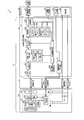
- FIG. 2 is a block diagram showing functions of main parts of the endoscope system according to Embodiment 1 of the present invention.
- FIG. 3 is a diagram schematically showing the configuration of the color filter.
- FIG. 4 is a circuit diagram showing a configuration of the first chip.
- FIG. 5 is a schematic diagram showing an outline of format conversion processing performed by the format conversion unit for even lines of the light receiving unit.
- FIG. 6 is a schematic diagram showing an outline of format conversion processing performed by the format conversion unit for odd lines of the light receiving unit.
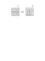
- FIG. 7 is a diagram schematically illustrating the conversion method of the filter conversion unit.
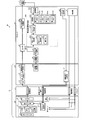
- FIG. 8 is a block diagram showing functions of main parts of the endoscope system according to Embodiment 2 of the present invention.
- an endoscope system including an imaging device will be described as a mode for carrying out the present invention (hereinafter referred to as “embodiment”). Further, the present invention is not limited by this embodiment. Further, in the description of the drawings, the same portions will be described with the same reference numerals. Furthermore, the drawings are schematic, and it should be noted that the relationship between the thickness and width of each member, the ratio of each member, and the like are different from the actual ones. Moreover, the part from which a mutual dimension and ratio differ also in between drawings.
- FIG. 1 is a diagram schematically showing an overall configuration of an endoscope system according to Embodiment 1 of the present invention.
- An endoscope system 1 shown in FIG. 1 includes an endoscope 2, a transmission cable 3, a connector unit 5, a processor 6 (processing device), a display device 7, and a light source device 8.
- the endoscope 2 captures an in-vivo image of the subject by inserting the insertion portion 100 which is a part of the transmission cable 3 into the body cavity of the subject, and outputs an image signal (image data) to the processor 6.
- the endoscope 2 is provided on one end side of the transmission cable 3 and on the distal end 101 side of the insertion unit 100 that is inserted into the body cavity of the subject, an imaging unit 20 (imaging device) that captures in-vivo images.
- the operation unit 4 that receives various operations on the endoscope 2 is connected to the proximal end 102 side of the insertion unit 100.
- the imaging unit 20 is connected to the connector unit 5 via the operation unit 4 by the transmission cable 3.
- the image signal of the image captured by the imaging unit 20 is output to the connector unit 5 through the transmission cable 3 having a length of several meters, for example.
- the connector unit 5 is connected to the endoscope 2, the processor 6, and the light source device 8, performs predetermined signal processing on the image signal output from the connected endoscope 2, and converts the imaging signal from an analog signal to a digital signal.
- the image is converted (A / D converted) and output to the processor 6 as an image signal.
- the processor 6 is configured by using a CPU (Central Processing Unit) or the like, performs predetermined image processing on the image signal output from the connector unit 5, and comprehensively controls the entire endoscope system 1.
- the processor 6 functions as a processing device.
- the display device 7 displays an image corresponding to the image signal subjected to image processing by the processor 6.
- the display device 7 displays various information related to the endoscope system 1.
- the light source device 8 is configured using, for example, a halogen lamp, a white LED (Light Emitting Diode), or the like, and is connected to the subject from the distal end 101 side of the insertion unit 100 of the endoscope 2 via the connector unit 5 and the transmission cable 3. Irradiate with illumination light.
- FIG. 2 is a block diagram showing functions of a main part of the endoscope system 1. With reference to FIG. 2, the detail of each part structure of the endoscope system 1 and the path
- the imaging unit 20 includes a first chip 21 (imaging element) and a second chip 22.
- the first chip 21 is two-dimensionally arranged in the matrix direction, receives light from the outside, generates an image signal corresponding to the amount of received light, and outputs the unit pixel 230 and the plurality of unit pixels 230.
- a light receiving unit 23 having a plurality of dummy pixels 247 that is provided for each transfer line (for each vertical transfer line) and generates and outputs a dummy signal used for image signal correction processing, and a predetermined unit pixel 230 in the light receiving unit 23.
- a readout unit 24 (readout circuit) that reads out an image signal and a dummy signal that are shared every time and photoelectrically converted by the light receiving unit 23 for each predetermined number of pixels, and a reference clock signal that is input from the connector unit 5 and synchronization
- a timing generation unit 25 that generates a timing signal based on the signal and outputs the timing signal to the reading unit 24; and a color detector provided on each light receiving surface of the plurality of unit pixels 230. It has a filter 26, a.
- the color filter 26 includes a red filter (hereinafter referred to as “R filter”) that transmits a red light component, and a first green filter (hereinafter referred to as “G r filter”) that transmits a green light component. ”), A Bayer composed of a second green filter that transmits a green light component (hereinafter referred to as“ Gb filter ”) and a blue filter that transmits a blue light component (hereinafter referred to as“ B filter ”).
- Gb filter green light component
- B filter blue filter that transmits a blue light component
- This is realized by using an array of Bayer filters T1 (RG r BG b ), and an R filter, a G r filter, a B filter, and a G b filter are arranged in each unit pixel 230.
- the color filter 26, in the even lines of the light receiving portion 23, are arranged alternately in the order of R filter and G r filters in the odd lines of the light receiving portion 23, alternately in the order of G b filter
- the second chip 22 includes a buffer 27 that functions as a transmission unit that transmits the image signal output from the first chip 21 to the processor 6 via the transmission cable 3 and the connector unit 5.
- the combination of the circuits mounted on the first chip 21 and the second chip 22 can be changed as appropriate according to the convenience of setting.
- the imaging unit 20 receives the power supply voltage VDD generated by the power supply unit 61 in the processor 6 through the transmission cable 3 together with the ground GND.
- a power supply stabilizing capacitor C1 is provided between the power supply voltage VDD supplied to the imaging unit 20 and the ground GND.
- the connector unit 5 includes an analog front end unit 51 (hereinafter referred to as “AFE unit 51”), an A / D conversion unit 52, an image signal processing unit 53, and a drive signal generation unit 57. Yes.
- the connector unit 5 is connected to the processor 6, electrically connects the endoscope 2 (imaging unit 20) and the processor 6, and functions as a relay processing unit that relays an electrical signal.
- the connector unit 5 and the imaging unit 20 are connected by a transmission cable 3, and the connector unit 5 and the processor 6 are connected by, for example, a coil cable.
- the connector unit 5 is also connected to the light source device 8.
- the AFE unit 51 receives the image signal transmitted from the imaging unit 20, performs impedance matching with a passive element such as a resistor, extracts an AC component with a capacitor, and determines an operating point with a voltage dividing resistor. Thereafter, the AFE unit 51 corrects the image signal (analog signal) and outputs it to the A / D conversion unit 52.
- the A / D conversion unit 52 converts the analog image signal input from the AFE unit 51 into a digital image signal and outputs the digital image signal to the image signal processing unit 53.
- the image signal processing unit 53 is configured by, for example, an FPGA (Field Programmable Gate Array), a reference clock signal (for example, a 27 MHz clock) serving as a reference for the operation of each component of the endoscope 2, and the start position of each frame Is generated and supplied to the timing generation unit 25, and predetermined signal processing such as noise removal, format conversion processing, and filter conversion processing is performed on the digital image signal input from the A / D conversion unit 52. I do.
- FPGA Field Programmable Gate Array
- a reference clock signal for example, a 27 MHz clock
- the image signal processing unit 53 includes at least a vertical line noise correction unit 531, a format conversion unit 532, a recording unit 533, a filter conversion unit 534, an endoscope control unit 535, and an ID information recording unit 536. Have.
- the vertical streak noise correction unit 531 corrects the vertical streak noise generated in the image signal input via the A / D conversion unit 52. Specifically, the vertical line noise correction unit 531 calculates a statistical value for each transfer line (vertical transfer line described later) in the output value of the dummy signal within a predetermined range output from the dummy pixel 247 a plurality of times.
- the correction data generation unit 531a that generates correction data for correcting the image signal output from the unit pixel 230 based on the calculation result for each transfer line, and the correction data for each transfer line generated by the correction data generation unit 531a.
- the correction of correcting the image signal by subtracting the correction data of the corresponding transfer line from the image signal output by the unit pixel 230 for each transfer line, and outputting the corrected image signal to the format conversion unit 532 Part 531b.
- the statistical value is one of an average value, a median value, and a mode value for each transfer line in the output value of the dummy signal within a predetermined range (normal value).
- the correction data generation unit 531a may generate correction data for each frame in which each of the plurality of unit pixels 230 generates an image signal, based on the output value of the dummy signal within a predetermined range.
- the format conversion unit 532 converts the image signal output from the first chip 21 into a predetermined format corresponding to the connected processor 6 and outputs it. Specifically, the format conversion unit 532 performs format conversion for converting the image signal input by correcting the vertical stripe noise from the vertical stripe noise correction unit 531 into an array of Bayer images.
- the format conversion unit 532 the 1-line horizontal signal in the even lines of the light receiving portion 23 reading unit 24 has read a plurality of image signals read out from pixels corresponding to the R filter and the G r filters
- the arrangement is converted so that a plurality of image signals read out from the pixels corresponding to 1 and 2 are alternated, and in the 1-line horizontal signal in the odd lines of the light receiving unit 23 read out by the reading unit 24, the Gb filter is used.
- the arrangement so that a plurality of image signals read out from the corresponding pixels and a plurality of image signals read out from the pixels corresponding to the B filter alternate, it is converted into a Bayer array image format. To do.
- the format conversion unit 532 converts each of the plurality of image signals read from the pixels corresponding to the R filter into odd-numbered vertical lines (in the one-line horizontal signal in the even lines of the light receiving unit 23 read by the reading unit 24. 2m + 1, 2n) in place, placing each of a plurality of image signals read out from pixels corresponding to G r filters to the even vertical lines (2m, 2n), and a light receiving portion for reading portion 24 has read in one line horizontal signal in 23 odd lines of the pixels arranged each of the plurality of image signals read out from pixels corresponding to G b filter odd vertical lines (2m + 1,2n + 1), corresponding to the B filter
- odd vertical lines 2m + 1,2n + 1
- a first line memory 533a for recording the image signal of the R filters format conversion is converted into an array of Bayer image by the format conversion unit 532, the second line memory 533b for recording an image signal of the G r filters When, and a third line memory 533c for recording an image signal of the B filter, and a fourth line memory 533d for recording an image signal of the G b filter, the.
- the filter conversion unit 534 converts the filter format of the image signal under the control of the endoscope control unit 535. Specifically, the filter conversion unit 534 converts the image signal of the Bayer filter into the image signal of the complementary color filter under the control of the endoscope control unit 535.
- the endoscope control unit 535 controls each unit constituting the image signal processing unit 53.
- the endoscope control unit 535 acquires the ID information of the processor 6 from the ID information recording unit 64 of the processor 6 and controls each unit based on the acquired information.
- the endoscope control unit 535 functions as an acquisition unit according to the first embodiment.
- the information necessary for controlling each unit is not limited to the ID information recording unit 64 described above, and a voltage level of a connector pin (not shown) or a combination thereof may be used as ID information.
- the ID information recording unit 536 includes identification information indicating the type of the endoscope 2, the type of the first chip 21 (for example, information on the color filter 26, a shared pixel method, etc.), format information and year type of the output image signal, etc. Record.
- the drive signal generator 57 is supplied from the processor 6, and is a synchronization that represents the start position of each frame based on a reference clock signal (for example, a 27 MHz clock signal) that serves as a reference for the operation of each component of the endoscope 2.
- a signal is generated and output to the timing generation unit 25 of the imaging unit 20 via the transmission cable 3 together with the reference clock signal.
- the synchronization signal generated by the drive signal generation unit 57 includes a horizontal synchronization signal and a vertical synchronization signal.
- the processor 6 is a control device that comprehensively controls the entire endoscope system 1.
- the processor 6 includes a power supply unit 61, an image signal processing unit 62, a clock generation unit 63, and an ID information recording unit 64.
- the power supply unit 61 generates a power supply voltage VDD, and supplies the generated power supply voltage VDD to the imaging unit 20 through the connector unit 5 and the transmission cable 3 together with the ground GND.
- the image signal processing unit 62 performs synchronization processing, white balance (WB) adjustment processing, gain adjustment processing, gamma correction processing, digital analog (for digital image signals subjected to signal processing by the image signal processing unit 53).
- WB white balance
- gamma correction processing digital analog (for digital image signals subjected to signal processing by the image signal processing unit 53).
- D / A) Image processing such as conversion processing and format conversion processing is performed to convert it into an image signal, and this image signal is output to the display device 7.
- the clock generation unit 63 outputs a reference clock signal to the drive signal generation unit 57.
- the ID information recording unit 64 records identification information indicating the type of the processor 6, type information indicating the type of color filter that can be processed by the image signal processing unit 62, format information and year that can be processed by the image signal processing unit 62. ID information to be recorded is recorded.
- the display device 7 displays the image captured by the imaging unit 20 based on the image signal input from the image signal processing unit 62.
- the display device 7 is configured using a display panel such as liquid crystal or organic EL (Electro Luminescence).
- FIG. 4 is a circuit diagram showing a configuration of the first chip 21.
- the first chip 21 includes a timing generation unit 25, an output unit 31 (amplifier), a vertical scanning unit 241 (row selection circuit), a constant current source 242 and a noise removal unit 243 (noise). Removal circuit), a column source follower transistor 244, and a horizontal scanning unit 245.
- a timing generation unit 25 an output unit 31 (amplifier), a vertical scanning unit 241 (row selection circuit), a constant current source 242 and a noise removal unit 243 (noise). Removal circuit), a column source follower transistor 244, and a horizontal scanning unit 245.
- the timing generation unit 25 generates various drive signals based on the reference clock signal and the synchronization signal, and sends them to the vertical scanning unit 241 (row selection circuit), the noise removal unit 243, and the horizontal scanning unit 245 of the reading unit 24 described later. Output each.
- the data is transferred to the vertical transfer line 239 and output to the noise removal unit 243.
- the vertical scanning unit 241 functions as a readout circuit, and reads out image signals from the two unit pixels 230 in a shared manner. Further, in the first embodiment, the vertical transfer line 239 functions as a transfer line.
- the noise removing unit 243 removes output variation of each unit pixel 230 and a noise signal at the time of pixel reset, and outputs an image signal photoelectrically converted by each unit pixel 230. Details of the noise removing unit 243 will be described later.
- the column selection signal ⁇ HCLK ⁇ N> is applied to the image signal, and the image signal photoelectrically converted by each unit pixel 230 is transferred to the horizontal transfer line 258 (second transfer line) via the noise removing unit 243 and output.
- the horizontal transfer line 258 functions as a transfer unit that transfers an image signal output from each unit pixel 230.
- Each unit pixel 230 includes a photoelectric conversion element 231 (photodiode) and a photoelectric conversion element 232, a charge conversion unit 233, a transfer transistor 234 (first transfer unit) and a transfer transistor 235, and a charge conversion unit reset unit 236 ( Transistor), a pixel source follower transistor 237, a pixel output switch 238 (signal output unit), and a dummy pixel 247 (reference signal generation unit).
- one or a plurality of photoelectric conversion elements and a transfer transistor for transferring signal charges from the respective photoelectric conversion elements to the charge conversion unit 233 are referred to as a unit cell. That is, the unit cell includes a set of one or a plurality of photoelectric conversion elements and transfer transistors, and each unit pixel 230 includes one unit cell.
- the photoelectric conversion element 231 and the photoelectric conversion element 232 photoelectrically convert incident light into a signal charge amount corresponding to the amount of light, and accumulate it.
- the photoelectric conversion element 231 and the photoelectric conversion element 232 have a cathode side connected to one end side of the transfer transistor 234 and the transfer transistor 235, respectively, and an anode side connected to the ground GND.
- the charge conversion unit 233 includes a floating diffusion capacitance (FD), and converts charges accumulated in the photoelectric conversion element 231 and the photoelectric conversion element 232 into a voltage.
- FD floating diffusion capacitance
- the transfer transistor 234 and the transfer transistor 235 transfer charges from the photoelectric conversion element 231 and the photoelectric conversion element 232 to the charge conversion unit 233, respectively.
- Signal lines to which drive pulses (row selection pulses) ⁇ Ta and ⁇ Tb are supplied are connected to the gates of the transfer transistor 234 and the transfer transistor 235, and the charge conversion unit 233 is connected to the other end side.
- the transfer transistor 234 and the transfer transistor 235 are turned on when the drive pulses ⁇ Ta and ⁇ Tb are supplied from the vertical scanning unit 241 via the signal lines, and signals are transmitted from the photoelectric conversion element 231 and the photoelectric conversion element 232 to the charge conversion unit 233. Transfer charge.
- the charge conversion unit reset unit 236 resets the charge conversion unit 233 to a predetermined potential.
- the charge conversion unit reset unit 236 has one end connected to the power supply voltage VDD, the other end connected to the charge conversion unit 233, and a gate connected to a signal line to which a drive pulse ⁇ R is supplied.
- ⁇ R is supplied from the vertical scanning unit 241 via the signal line from the vertical scanning unit 241
- the charge conversion unit reset unit 236 is turned on, releases the signal charge accumulated in the charge conversion unit 233, and causes the charge conversion unit 233 to have a predetermined potential. Reset to.
- One end of the pixel source follower transistor 237 is connected to the power supply voltage VDD, the other end is connected to one end of the pixel output switch 238, and a signal (image signal or reset signal) that has been voltage-converted by the charge conversion unit 233 is connected to the gate. Signal) is input.
- the pixel output switch 238 outputs the signal voltage-converted by the charge conversion unit 233 to the vertical transfer line 239.
- the other end of the pixel output switch 238 is connected to the vertical transfer line 239, and a signal line to which the drive pulse ⁇ X is supplied is connected to the gate.
- the pixel output switch 238 is turned on when the drive pulse ⁇ X is supplied to the gate of the pixel output switch 238 from the vertical scanning unit 241 via the signal line, and transfers the image signal or the reset signal to the vertical transfer line 239. To do.
- the dummy pixel 247 is provided for each transfer line of the unit pixel 230.
- the dummy pixel 247 includes a pixel reset unit 236a and a pixel source follower transistor 237a. That is, the photoelectric conversion element 231 (photodiode), the charge conversion unit 233, and the transfer transistor 234 (first transfer unit) are omitted from the unit pixel 230.
- the pixel reset unit 236a fixes the gate of the pixel source follower transistor 237a at a predetermined potential.
- the pixel reset unit 236a has one end connected to the power supply voltage VR, the other end connected to the gate of the pixel source follower transistor 237a, and a signal line to which the drive signal ⁇ Rdmy is supplied connected to the gate.
- One end of the pixel source follower transistor 237a is connected to the power supply voltage VR supplied from a reference voltage generator (not shown), the other end is connected to the vertical transfer line 239, and a predetermined potential (VRdmy) is input to the gate. Is done.
- a dummy signal columnumn reference signal
- a dummy signal columnumn reference signal
- the gate of the pixel reset unit 236a is input.
- VDD level for example, 3.3V
- VRdmy for example, 2V
- the gate of the pixel reset unit 236a is input.
- the drive signal ⁇ Rdmy is supplied, the pixel source follower transistor 237a is turned on, and the dummy pixel 247 including the pixel reset unit 236a is selected (selection operation).
- the drive signal ⁇ Rdmy is supplied to the gate of the pixel reset unit 236a when the power supply voltage VR is at the non-selection voltage level (eg, 1V) and VRdmy (eg, 1V)
- the pixel source follower transistor 237a is turned off. The selection of the dummy pixel 247 including the pixel reset unit 236a is released (non-selection operation).
- the constant current source 242 has one end connected to the vertical transfer line 239, the other end connected to the ground GND, and a bias voltage Vbias1 applied to the gate.
- the constant current source 242 drives the unit pixel 230 with the constant current source 242 and reads the output of the unit pixel 230 to the vertical transfer line 239.
- the signal read to the vertical transfer line 239 is input to the noise removing unit 243.
- the noise removing unit 243 includes a transfer capacitor 252 (AC coupling capacitor) and a clamp switch 253 (transistor).
- the transfer capacitor 252 has one end connected to the vertical transfer line 239 and the other end connected to the column source follower transistor 244.
- the clamp switch 253 has one end connected to a signal line to which a clamp voltage Vclp is supplied from a reference voltage generator (not shown). The other end side of the clamp switch 253 is connected between the transfer capacitor 252 and the column source follower transistor 244, and the drive signal ⁇ VCL is input from the timing generation unit 25 to the gate.
- the image signal input to the noise removing unit 243 is an optical noise sum signal including a noise component.
- the transfer capacitor 252 turns on the clamp switch 253, and the clamp voltage Vclp supplied from the reference voltage generation unit (not shown). It is reset by.
- the image signal from which noise is removed by the noise removing unit 243 is input to the gate of the column source follower transistor 244.
- the noise removing unit 243 configured as described above does not require a sampling capacitor (sampling capacity), the capacity of the transfer capacity (AC coupling capacitor) 252 is sufficient with respect to the input capacity of the column source follower transistor 244. If it is. In addition, the noise removing unit 243 can reduce the area occupied by the first chip 21 because of the absence of the sampling capacity.
- One end of the column source follower transistor 244 is connected to the power supply voltage VDD, the other end is connected to one end of the column selection switch 254 (second transfer unit), and noise is removed by the noise removing unit 243 at the gate. A signal is input.
- the column selection switch 254 has one end connected to the other end of the column source follower transistor 244, the other end connected to the horizontal transfer line 258 (second transfer line), and a gate from the horizontal scanning unit 245 to the drive signal ⁇ HCLK.
- a signal line for supplying ⁇ M> is connected.
- the column selection switch 254 is turned on when the drive signal ⁇ HCLK ⁇ M> is supplied from the horizontal scanning unit 245 to the gate of the column selection switch 254 of the column ⁇ M>, and the signal of the vertical transfer line 239 of the column ⁇ M>.
- the image signal from which noise has been removed by the noise removing unit 243 is transferred to the horizontal transfer line 258.
- the horizontal reset transistor 256 has one end connected to the ground GND, the other end connected to the horizontal transfer line 258, and a gate to which the drive signal ⁇ HCLR is input from the timing generator 25.
- the horizontal reset transistor 256 is turned on when the drive signal ⁇ HCLR is input from the timing generation unit 25 to the gate of the horizontal reset transistor 256 and resets the horizontal transfer line 258.
- the constant current source 257 has one end connected to the horizontal transfer line 258, the other end connected to the ground GND, and a bias voltage Vbias2 applied to the gate.
- the constant current source 257 reads the image signal from the vertical transfer line 239 to the horizontal transfer line 258.
- the image signal or dummy signal read to the horizontal transfer line 258 is input to the output unit 31.
- the output unit 31 amplifies and outputs the image signal from which noise has been removed and a dummy signal (a reference signal serving as a reference when correcting the transfer line) as necessary (Vout).
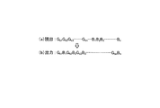
- FIG. 5 is a schematic diagram illustrating an outline of the format conversion process performed by the format conversion unit 532 for the even lines of the light receiving unit 23.
- FIG. 6 is a schematic diagram showing an outline of format conversion processing performed by the format conversion unit 532 for odd lines of the light receiving unit 23.
- 5 (a) and 6 (a) show an example of an image signal inputted by correcting vertical streak noise from the vertical streak noise correcting unit 531
- FIGS. 5 (b) and 6 (b) show format conversion. An example of the image signal after the format conversion by the unit 532 is shown.
- FIG. 5 is a schematic diagram illustrating an outline of the format conversion process performed by the format conversion unit 532 for the even lines of the light receiving unit 23.
- FIG. 6 is a schematic diagram showing an outline of format conversion processing performed by the format conversion unit 532 for odd lines of the light receiving unit 23.
- 5 (a) and 6 (a) show an example of an image signal inputted by correcting vertical streak noise from the vertical streak noise correcting unit 531
- the format conversion unit 532 performs format conversion for converting the image signal input by correcting the vertical streak noise from the vertical streak noise correction unit 531 into an array of Bayer images. Specifically, the format conversion unit 532 converts the image signals of all R filters into odd lines (2m + 1, 2n) of odd vertical lines in one line horizontal signal in the even lines (2n) of the light receiving unit 23 (imaging device). together it is recorded in the first line memory 533a disposed in), even lines (2m of all image signals vertical line G r filters, is recorded in the second line memory 533b arranged in 2n). More specifically, as shown in FIG.
- the format conversion unit 532 generates a vertical signal from the vertical streak noise correction unit 531 in the 1-line horizontal signal in the even line (2n) of the light receiving unit 23 (imaging device).
- An array of Bayer images by alternately switching the image signals (R 1 to R n ) of the R filter and the image signals (G r1 to G rn ) of the G r filter of the image signal input after correcting the streak noise (R 1 G r1 R 2 G r2 ... R n G rn ).
- the format conversion unit 532 records the image signal converted into the Bayer array in each of the first line memory 533a and the second line memory 533b.
- the format conversion unit 532 converts the image signals of all the B filters to the odd lines (2m + 1, 2n + 1) of the vertical lines in one line horizontal signal in the odd lines (2n + 1) of the light receiving unit 23 (imaging device). causes recorded arranged to third line memories 533c in), even lines (2m all G b filters an image signal vertical lines, 2n + 1) disposed in is recorded in the fourth line memory 533d. More specifically, as shown in FIG.
- the format conversion unit 532 receives a vertical signal from the vertical streak noise correction unit 531 in the 1-line horizontal signal in the odd-numbered line (2n + 1) of the light receiving unit 23 (imaging device).
- An array of Bayer images by alternately switching the image signals (B 1 to B n ) of the B filter and the image signals (G b1 to G bn ) of the G r filter of the input image signal with the line noise corrected. (G b1 B 1 G b2 B 2 ... G bn B n ).
- the format conversion unit 532 records the image signal converted into the Bayer array in each of the third line memory 533c and the fourth line memory 533d.
- the format conversion unit 532 converts the image signals of all the R filters in the horizontal signal of one line in the even-numbered line (2n) of the image signal input by correcting the vertical stripe noise from the vertical stripe noise correction unit 531.
- second line arranged with is recorded in the first line memory 533a disposed in the odd lines (2m + 1, 2n) of the vertical line, the image signals of all G r filters to the even lines in the vertical line (2m, 2n) In the 1-line horizontal signal in the odd line (2n + 1) of the light receiving unit 23 (image sensor), all the B filter image signals are arranged in the odd line (2m + 1, 2n + 1) of the vertical line.
- the filter conversion unit 534 Under the control of the endoscope control unit 535, the filter conversion unit 534 outputs a Bayer array image signal from each of the first line memory 533a, the second line memory 533b, the third line memory 533c, and the fourth line memory 533d.
- the acquired Bayer array image signal is converted into a color filter compatible with the processor 6.
- the endoscope control unit 535 uses the filter conversion unit 534 based on the color filter type that can be processed by the image signal processing unit 62 included in the ID information acquired from the ID information recording unit 64 of the processor 6.
- the processor 6 converts the filter into a compatible type. More specifically, as shown in FIG. 7, when the image signal processing unit 62 of the processor 6 is compatible with the complementary color filter, the filter conversion unit 534 converts the image signal of the Bayer filter into the image signal of the complementary color filter. And output to the image signal processing unit 62.
- the filter conversion unit 534 generates an odd number that configures an image based on Bayer array image signals acquired from each of the first line memory 533a, the second line memory 533b, the third line memory 533c, and the fourth line memory 533d.
- image signals of complementary colors of cyan hereinafter referred to as “Cy filter” and green (hereinafter referred to as “G filter”) are generated, and in an even line, yellow (hereinafter referred to as “Y filter”) and magenta.
- Y filter yellow
- Mg filter A complementary color image signal
- the filter converter 534 the G b filters recorded in the image signal of the B filters recorded in the third line memory 533c (the blue component)
- the fourth line memory 533d By using the image signal (second green component) and calculating the image signal of the Cy filter and the image signal of the G filter in the complementary color filter, the image signal of the Bayer filter T1 is converted to the image signal of the complementary color filter T2. .
- the filter conversion unit 534 an image signal of Cy filter in a complementary color filter, the image signal of the B filters recorded in the third line memory 533c and G b filters recorded in the fourth line memory 533d calculated by adding the image signal is calculated by using the G b image signals of filters recorded G filter in the fourth line memory 533d in complementary color filter T2.
- the filter conversion unit 534 image signals of R filters recorded in the first line memory 533a (the red component), the image signal of the G r filters recorded in the second line memory 533b (first green component) And the image signal of the B filter (blue component) recorded in the third line memory 533c, and the image signal of the Mg filter (magenta component) and the image signal of the Y filter (yellow component) in the complementary color filter.
- the image signal of the Bayer filter T1 is converted into the image signal of the complementary color filter T2.
- the filter conversion unit 534 an image signal of the Y filter in a complementary color filter, the image signal of the R filters recorded in the first line memory 533a and G r filters recorded in the second line memory 533b image calculated by adding the signal, the image signal and an image signal of the G r filters recorded in the second line memory 533b of R filters recording picture signals of Mg filter in a complementary color filter T2 in the first line memory 533a And the image signal of the B filter recorded in the third line memory 533c are calculated.
- the filter conversion unit 534 is configured to perform Bayer array from each of the first line memory 533a, the second line memory 533b, the third line memory 533c, and the fourth line memory 533d under the control of the endoscope control unit 535. And the acquired Bayer array image signal is converted into an image signal of a color filter compatible with the processor 6.
- the filter conversion unit 534 does not perform the filter conversion, and the image of the color components in the first line memory 533a to the fourth line memory 533d.
- the image signal is output to the processor 6 without converting the signal.
- the processor 6 does not have to be provided with the image signal processing unit 62 corresponding to the Bayer array filter, which is convenient for the user and excellent in versatility.
- all the 1-line horizontal signals of the even lines (2n) of the image signal input by the format conversion unit 532 with the vertical stripe noise corrected from the vertical stripe noise correction unit 531 are all included.
- the R filter image signal in the vertical line odd lines of (2m + 1, 2n) causes recorded in the first line memory 533a disposed on
- all G r filtered image signal vertical lines of the even lines of the (2m, 2n) Are arranged in the second line memory 533b and recorded in the odd line (2m + 1, 2n + 1) in the odd line (2m + 1, 2n + 1) of the vertical line.
- the filter conversion unit 534 is controlled by the endoscope control unit 535, and the first line memory 533a, the second line memory 533b, the third line memory 533c, and the fourth line memory.
- the Bayer array image signal is acquired from each of 533d, and the acquired Bayer array image signal is converted into a filter compatible with the processor 6.
- the image signal of the Bayer filter is converted into the image signal of the complementary color filter, which is convenient for the user and excellent in versatility.
- the format conversion unit 532 performs format conversion on the image signal input with the vertical stripe noise corrected from the vertical stripe noise correction unit 531, and thus a high-quality image is obtained. be able to.
- the endoscope 2 changes the content of the image signal to be output according to the type of the processor 6.
- the processor changes the image according to the endoscope. Change the content of the process.
- the same components as those in the endoscope system 1 according to Embodiment 1 described above are denoted by the same reference numerals, and description thereof is omitted.
- FIG. 8 is a block diagram showing functions of main parts of the endoscope system according to Embodiment 2 of the present invention.
- the endoscope system 1a includes an endoscope 2a, a processor 6a, and a display device 7.
- the endoscope 2a has a color filter 26a and a connector part 5a instead of the color filter 26 and the connector part 5 of the first chip 21 of the endoscope 2 according to the first embodiment described above.
- the color filter 26a is configured using a complementary color filter (CyGYMg) (for example, the complementary color filter T2 in FIG. 7).
- the connector unit 5a includes an AFE unit 51, an A / D conversion unit 52, an image signal processing unit 53a, an ID information recording unit 536, and a drive signal generation unit 57.
- the image signal processing unit 53a is configured by, for example, an FPGA, and generates a reference clock signal (for example, a 27 MHz clock) serving as a reference for the operation of each component of the endoscope 2a and a synchronization signal indicating the start position of each frame. Then, the signal is supplied to the timing generation unit 25 and predetermined signal processing such as noise removal is performed on the digital image signal input from the A / D conversion unit 52.
- a reference clock signal for example, a 27 MHz clock
- the processor 6a includes a power supply unit 61, a first image signal processing unit 62a, a second image signal processing unit 62b, a clock generation unit 63, an ID information acquisition unit 65, a switching unit 66, and an image processing control unit 67. .
- the first image signal processing unit 62a performs a synchronization process on the digital image signal (image signal of the complementary color filter) subjected to the signal processing by the image signal processing unit 53a input via the switching unit 66, and performs white processing.
- Image processing such as balance (WB) adjustment processing, gain adjustment processing, gamma correction processing, digital analog (D / A) conversion processing, format conversion processing, etc. is performed and converted into an image signal, and this image signal is output to the display device 7 To do.
- the second image signal processing unit 62b performs format conversion processing and filtering on the digital image signal (Bayer filter image signal) subjected to signal processing by the image signal processing unit 53a input via the switching unit 66.
- Image processing such as conversion processing, synchronization processing, white balance (WB) adjustment processing, gain adjustment processing, gamma correction processing, and digital analog (D / A) conversion processing is performed to convert the image signal, and this image signal is displayed.
- the second image signal processing unit 62b includes at least the vertical streak noise correction unit 531, the format conversion unit 532, the recording unit 533, and the filter conversion unit 534 according to Embodiment 1 described above.
- the ID information acquisition unit 65 acquires the ID information of the endoscope 2a from the ID information recording unit 536 of the endoscope 2a connected to the processor 6a, and outputs the acquired ID information to the image processing control unit 67.
- the switching unit 66 switches the output destination of the image signal input from the endoscope 2a according to the type of the endoscope 2a connected to the processor 6a under the control of the image processing control unit 67.
- the image processing control unit 67 is configured using a CPU or the like, and comprehensively controls the operation of each component of the processor 6a. Further, the image processing control unit 67 switches the output destination of the image signal input from the endoscope 2 a by controlling the switching unit 66 based on the ID information input from the ID information acquisition unit 65. Specifically, when the filter information of the endoscope 2a included in the ID information input from the ID information recording unit 536 is a complementary color filter, the image processing control unit 67 outputs an image signal input from the endoscope 2a.
- the switching unit 66 When the switching unit 66 is switched so as to be input to the first image signal processing unit 62a, and the filter information of the endoscope 2a included in the ID information input from the ID information acquisition unit 65 is a Bayer filter, the endoscope 2a The switching unit 66 is switched so that the image signal input from is input to the second image signal processing unit 62b.
- the two first image signal processing units 62a and the second image signal processing unit 62b that can respectively correspond to the Bayer filter and the complementary color filter are provided, and image processing control is performed.
- the output destination to which the switching unit 66 outputs the image signal is the first image signal processing unit 62a or the second image signal processing unit 62b. Switch to.
- the image signal processing unit is provided in the connector unit, but may be provided, for example, in the operation unit of the endoscope.
- the present invention can include various embodiments not described herein, and various design changes can be made within the scope of the technical idea specified by the claims. It is.
Landscapes
- Engineering & Computer Science (AREA)
- Health & Medical Sciences (AREA)
- Life Sciences & Earth Sciences (AREA)
- Surgery (AREA)
- Multimedia (AREA)
- Signal Processing (AREA)
- Physics & Mathematics (AREA)
- Optics & Photonics (AREA)
- Biomedical Technology (AREA)
- General Health & Medical Sciences (AREA)
- Radiology & Medical Imaging (AREA)
- Nuclear Medicine, Radiotherapy & Molecular Imaging (AREA)
- Biophysics (AREA)
- Heart & Thoracic Surgery (AREA)
- Medical Informatics (AREA)
- Molecular Biology (AREA)
- Animal Behavior & Ethology (AREA)
- Pathology (AREA)
- Public Health (AREA)
- Veterinary Medicine (AREA)
- Astronomy & Astrophysics (AREA)
- General Physics & Mathematics (AREA)
- Endoscopes (AREA)
- Color Television Image Signal Generators (AREA)
- Instruments For Viewing The Inside Of Hollow Bodies (AREA)
- Studio Devices (AREA)
Abstract
使用者にとって利便性が高く、汎用性に優れる内視鏡を提供する。2次元状に配置された単位画素(230)を有し、単位画素(230)の各々が光を受光して画像信号を生成する第1チップ(21)を備え、画像信号に対して画像処理を施して表示装置(7)に出力する複数のプロセッサ(6)のいずれかに接続される内視鏡(2)であって、第1チップ(21)が出力した 画像信号を所定のフォーマットに変換して出力するフォーマット変換部(532)と、フォーマット変換部(532)が設けられ、プロセッサ(6)に接続されるコネクタ部(5)と、を備える。
Description
本発明は、生体内に導入され、該生体内の画像を取得する内視鏡に関する。
近年、内視鏡等の撮像装置において、被写体の輪郭を強調した画像信号を生成する技術が知られている(特許文献1参照)。この技術によれば、ベイヤー配列のカラーフィルタが設けられた撮像素子の水平ラインにおける奇数ラインおよび偶数ラインの各々から画像信号を露光時に交互に読み出して混合した第1の混合信号と、奇数ラインおよび偶数ラインの各々から画像信号を非露光時に交互に読み出して混合した第2の混合信号と、を用いることによって、被写体の輪郭を強調した画像信号を生成する。
しかしながら、上述した特許文献1では、ベイヤー配列のカラーフィルタが設けられた撮像素子を備えた内視鏡の画像処理しか考慮されていなかった。このため、所定の画素数毎に読み出し回路を共有する画素共有方式の撮像素子を備えた内視鏡が出力する画像信号に対して、画像処理を行う場合、処理装置内に画素共有方式の撮像素子に対応可能な画像処理の回路を設けたり、内視鏡毎に処理装置を設けたりしなければならず、使用者にとって利便性が低く、汎用性に乏しかった。
本発明は、上記に鑑みてなされたものであって、使用者にとって利便性が高く、汎用性に優れる内視鏡を提供することを目的とする。
上述した課題を解決し、目的を達成するために、本発明に係る内視鏡は、2次元状に配置され、外部から光を受光し、受光量に応じた画像信号を生成する複数の画素と、所定の画素数毎に共有されて前記画像信号を転送線に読み出す複数の読み出し回路と、を有する撮像素子を備え、前記画像信号に対して画像処理を施す処理装置に接続される内視鏡であって、前記撮像素子が出力した前記画像信号を、接続される前記処理装置に応じた所定のフォーマットに変換して出力するフォーマット変換部と、前記フォーマット変換部が設けられ、前記処理装置に接続されるコネクタ部と、を備えたことを特徴とする。
また、本発明に係る内視鏡は、上記発明において、前記撮像素子は、前記複数の画素の配置における前記転送線毎に設けられ、前記画像信号の補正処理に用いられるダミー信号を生成して出力する複数のダミー画素と、を有し、前記ダミー画素から複数回出力された前記ダミー信号の出力値の前記転送線毎の統計値を算出し、該算出した算出結果に基づいて前記画像信号を補正するための補正データを前記転送線毎に生成する補正データ生成部と、前記補正データ生成部が生成した前記補正データに基づいて、前記画像信号を補正する補正部と、を備え、前記フォーマット変換部は、前記補正部が補正した前記画像信号を前記所定のフォーマットに変換することを特徴とする。
また、本発明に係る内視鏡は、上記発明において、前記撮像素子は、前記複数の画素における水平ラインの偶数ラインにおいて、赤色の成分を透過させる赤色フィルタおよび緑色の成分を透過させる第1の緑色フィルタが交互に配置され、かつ、前記複数の画素における水平ラインの奇数ラインにおいて、緑色の成分を透過させる第2の緑色フィルタおよび青色の成分を透過させる青色フィルタが交互に配置されたベイヤー配列のカラーフィルタを有し、前記読み出し回路は、前記撮像素子における水平ラインの偶数ラインにおいて、前記赤色フィルタに対応する画素から前記画像信号および前記第1の緑色フィルタに対応する画素から前記画像信号をそれぞれ読み出し、かつ、前記撮像素子の奇数ラインにおいて、前記第2の緑色フィルタに対応する画素から前記画像信号および前記青色フィルタに対応する画素から前記画像信号をそれぞれ読み出し、前記フォーマット変換部は、前記読み出し回路が読み出した前記撮像素子の偶数ラインにおいて、前記赤色フィルタに対応する画素から読み出された複数の前記画像信号と前記第1の緑色フィルタに対応する画素から読み出された複数の前記画像信号とが交互になるように配置を変換し、かつ、前記読み出し回路が読み出した前記撮像素子の奇数ラインにおいて、前記第2の緑色フィルタに対応する画素から読み出された複数の前記画像信号と前記青色フィルタに対応する画素から読み出された複数の前記画像信号とが交互になるように配置を変換することによって、ベイヤー配列の画像のフォーマットに変換することを特徴とする。
また、本発明に係る内視鏡は、上記発明において、接続される前記処理装置から該処理装置の処理可能なカラーフィルタの種別を示す種別情報を含む識別情報を取得する取得部と、前記取得部が取得した前記識別情報に基づいて、前記フォーマット変換部が変換した前記画像信号を前記処理装置が対応可能なカラーフィルタの画像信号に変換するフィルタ変換部と、をさらに備えたことを特徴とする。
本発明によれば、使用者にとって利便性が高く、汎用性に優れるという効果を奏する。
以下、本発明を実施するための形態(以下、「実施の形態」という)として、撮像装置を備えた内視鏡システムについて説明する。また、この実施の形態により、本発明が限定されるものではない。さらに、図面の記載において、同一の部分には同一の符号を付して説明する。さらにまた、図面は、模式的なものであり、各部材の厚みと幅との関係、各部材の比率等は、現実と異なることに留意する必要がある。また、図面の相互間においても、互いの寸法や比率が異なる部分が含まれている。
(実施の形態1)
〔内視鏡システムの構成〕
図1は、本発明の実施の形態1に係る内視鏡システムの全体構成を模式的に示す図である。図1に示す内視鏡システム1は、内視鏡2と、伝送ケーブル3と、コネクタ部5と、プロセッサ6(処理装置)と、表示装置7と、光源装置8と、を備える。
〔内視鏡システムの構成〕
図1は、本発明の実施の形態1に係る内視鏡システムの全体構成を模式的に示す図である。図1に示す内視鏡システム1は、内視鏡2と、伝送ケーブル3と、コネクタ部5と、プロセッサ6(処理装置)と、表示装置7と、光源装置8と、を備える。
内視鏡2は、伝送ケーブル3の一部である挿入部100を被検体の体腔内に挿入することによって被検体の体内画像を撮像して画像信号(画像データ)をプロセッサ6へ出力する。また、内視鏡2は、伝送ケーブル3の一端側であり、被検体の体腔内に挿入される挿入部100の先端101側に、体内画像の撮像を行う撮像部20(撮像装置)が設けられ、挿入部100の基端102側に、内視鏡2に対する各種操作を受け付ける操作部4が接続される。撮像部20は、伝送ケーブル3により、操作部4を介してコネクタ部5に接続される。撮像部20が撮像した画像の画像信号は、例えば、数mの長さを有する伝送ケーブル3を通り、コネクタ部5に出力される。
コネクタ部5は、内視鏡2、プロセッサ6および光源装置8に接続され、接続された内視鏡2が出力する画像信号に所定の信号処理を施すとともに、撮像信号をアナログ信号からデジタル信号に変換(A/D変換)して画像信号としてプロセッサ6へ出力する。
プロセッサ6は、CPU(Central Processing Unit)等を用いて構成され、コネクタ部5から出力される画像信号に所定の画像処理を施すとともに、内視鏡システム1全体を統括的に制御する。なお、本実施の形態1では、プロセッサ6が処理装置として機能する。
表示装置7は、プロセッサ6が画像処理を施した画像信号に対応する画像を表示する。また、表示装置7は、内視鏡システム1に関する各種情報を表示する。
光源装置8は、例えばハロゲンランプや白色LED(Light Emitting Diode)等を用いて構成され、コネクタ部5、伝送ケーブル3を経由して内視鏡2の挿入部100の先端101側から被検体へ向けて照明光を照射する。
図2は、内視鏡システム1の要部の機能を示すブロック図である。図2を参照して、内視鏡システム1の各部構成の詳細および内視鏡システム1内の電気信号の経路を説明する。
図2に示すように、撮像部20は、第1チップ21(撮像素子)と、第2チップ22と、を備える。
第1チップ21は、行列方向に2次元状に配置され、外部から光を受光し、受光量に応じた画像信号を生成して出力する複数の単位画素230および複数の単位画素230の配置における転送線毎(垂直転送線毎)に設けられ、画像信号の補正処理に用いられるダミー信号を生成して出力する複数のダミー画素247を有する受光部23と、受光部23における所定の単位画素230毎に共用されて受光部23で光電変換された画像信号およびダミー信号を所定の画素数毎に共用されて読み出す読み出し部24(読み出し回路)と、コネクタ部5から入力された基準クロック信号および同期信号に基づきタイミング信号を生成して読み出し部24に出力するタイミング生成部25と、複数の単位画素230の各々の受光面に設けられたカラーフィルタ26と、を有する。なお、第1チップ21のより詳細な構成については、図4を参照して後述する。
カラーフィルタ26は、図3に示すように、赤色の光成分を透過させる赤色フィルタ(以下、「Rフィルタ」という)、緑色の光成分を透過させる第1の緑色フィルタ(以下、「Grフィルタ」という)、緑色の光成分を透過させる第2の緑色フィルタ(以下、「Gbフィルタ」という)および青色の光成分を透過させる青色フィルタ(以下、「Bフィルタ」という)で構成されたベイヤー配列のベイヤーフィルタT1(RGrBGb)を用いて実現され、各単位画素230にRフィルタ、Grフィルタ、BフィルタおよびGbフィルタが配置される。具体的には、カラーフィルタ26は、受光部23の偶数ラインにおいて、RフィルタおよびGrフィルタの順で交互に配置され、受光部23の奇数ラインにおいて、GbフィルタおよびBフィルタの順で交互に配置される。
第2チップ22は、伝送ケーブル3およびコネクタ部5を介して、第1チップ21から出力される画像信号をプロセッサ6へ送信する送信部として機能するバッファ27を有する。なお、第1チップ21と第2チップ22に搭載される回路の組み合わせは設定の都合に合わせて適宜変更可能である。
また、撮像部20は、伝送ケーブル3を介してプロセッサ6内の電源部61で生成された電源電圧VDDをグランドGNDとともに受け取る。撮像部20に供給される電源電圧VDDとグランドGNDとの間には、電源安定用のコンデンサC1が設けられている。
コネクタ部5は、アナログ・フロント・エンド部51(以下、「AFE部51」という)と、A/D変換部52と、画像信号処理部53と、駆動信号生成部57と、が設けられている。コネクタ部5は、プロセッサ6に接続され、内視鏡2(撮像部20)とプロセッサ6とを電気的に接続し、電気信号を中継する中継処理部として機能する。コネクタ部5と撮像部20とは、伝送ケーブル3で接続され、コネクタ部5とプロセッサ6とは、例えば、コイルケーブルにより接続される。また、コネクタ部5は、光源装置8にも接続されている。
AFE部51は、撮像部20から伝送される画像信号を受信し、抵抗などの受動素子でインピーダンスマッチングを行った後、コンデンサで交流成分を取り出し、分圧抵抗で動作点を決定する。その後、AFE部51は、画像信号(アナログ信号)を補正してA/D変換部52へ出力する。
A/D変換部52は、AFE部51から入力されたアナログの画像信号をデジタルの画像信号に変換して画像信号処理部53へ出力する。
画像信号処理部53は、例えば、FPGA(Field Programmable Gate Array)により構成され、内視鏡2の各構成部の動作の基準となる基準クロック信号(例えば、27MHzのクロック)および各フレームのスタート位置を表す同期信号を生成して、タイミング生成部25に供給するとともに、A/D変換部52から入力されるデジタル画像信号に対してノイズ除去、フォーマット変換処理、フィルタ変換処理等の所定の信号処理を行う。
ここで、画像信号処理部53の詳細な構成について説明する。画像信号処理部53は、少なくとも、縦筋ノイズ補正部531と、フォーマット変換部532と、記録部533と、フィルタ変換部534と、内視鏡制御部535と、ID情報記録部536と、を有する。
縦筋ノイズ補正部531は、A/D変換部52を介して入力される画像信号に生じている縦筋ノイズを補正する。具体的には、縦筋ノイズ補正部531は、ダミー画素247から複数回出力された所定の範囲内であるダミー信号の出力値における転送線毎(後述する垂直転送線)の統計値を算出し、この算出結果に基づいて単位画素230が出力した画像信号を補正するための補正データを転送線毎に生成する補正データ生成部531aと、補正データ生成部531aが生成した転送線毎の補正データに基づいて、転送線毎の単位画素230が出力する画像信号から該当する転送線の補正データを減算することによって、画像信号を補正し、この補正した画像信号をフォーマット変換部532へ出力する補正部531bと、を有する。ここで、統計値とは、所定の範囲内(正常値)であるダミー信号の出力値における転送線毎の平均値、中央値および最頻値のいずれかである。なお、補正データ生成部531aは、所定の範囲内であるダミー信号の出力値を、複数の単位画素230の各々が画像信号を生成する1フレーム毎に補正データを生成してもよい。
フォーマット変換部532は、第1チップ21が出力した画像信号を、接続されるプロセッサ6に応じた所定のフォーマットに変換して出力する。具体的には、フォーマット変換部532は、縦筋ノイズ補正部531から縦筋ノイズが補正されて入力された画像信号をベイヤー画像の配列に変換するフォーマット変換を行う。より具体的には、フォーマット変換部532は、読み出し部24が読み出した受光部23の偶数ラインにおける1ライン水平信号において、Rフィルタに対応する画素から読み出された複数の画像信号とGrフィルタに対応する画素から読み出された複数の画像信号とが交互になるように配置を変換し、かつ、読み出し部24が読み出した受光部23の奇数ラインにおける1ライン水平信号において、Gbフィルタに対応する画素から読み出された複数の画像信号とBフィルタに対応する画素から読み出された複数の画像信号とが交互になるように配置を変換することによって、ベイヤー配列の画像のフォーマットに変換する。たとえば、フォーマット変換部532は、読み出し部24が読み出した受光部23の偶数ラインにおける1ライン水平信号において、Rフィルタに対応する画素から読み出された複数の画像信号の各々を奇数の垂直ライン(2m+1,2n)に配置し、Grフィルタに対応する画素から読み出された複数の画像信号の各々を偶数の垂直ライン(2m,2n)に配置し、かつ、読み出し部24が読み出した受光部23の奇数ラインにおける1ライン水平信号において、Gbフィルタに対応する画素から読み出された複数の画像信号の各々を奇数の垂直ライン(2m+1,2n+1)に配置し、Bフィルタに対応する画素から読み出された複数の画像信号の各々を偶数の垂直ライン(2m,2n+1)に配置することによって、ベイヤー配列の画像のフォーマットに変換する。
記録部533は、フォーマット変換部532によってフォーマット変換がベイヤー画像の配列に変換されたRフィルタの画像信号を記録する第1ラインメモリ533aと、Grフィルタの画像信号を記録する第2ラインメモリ533bと、Bフィルタの画像信号を記録する第3ラインメモリ533cと、Gbフィルタの画像信号を記録する第4ラインメモリ533dと、を有する。
フィルタ変換部534は、内視鏡制御部535の制御のもと、画像信号のフィルタのフォーマットを変換する。具体的には、フィルタ変換部534は、内視鏡制御部535の制御のもと、ベイヤーフィルタの画像信号を補色フィルタの画像信号に変換する。
内視鏡制御部535は、画像信号処理部53を構成する各部を制御する。内視鏡制御部535は、プロセッサ6のID情報記録部64からプロセッサ6のID情報を取得し、取得した情報に基づいて、各部を制御する。なお、内視鏡制御部535が本実施の形態1に係る取得部として機能する。また、各部制御に必要な情報を取得するのは、上述したID情報記録部64に限らず、図示しないコネクタピンの電圧レベルやその組み合せをID情報として使用しても良い。
ID情報記録部536は、内視鏡2の種別を示す識別情報、第1チップ21の種別(例えば、カラーフィルタ26の情報や共有画素方式等)、出力する画像信号のフォーマット情報および年式等を記録する。
駆動信号生成部57は、プロセッサ6から供給され、内視鏡2の各構成部の動作の基準となる基準クロック信号(例えば、27MHzのクロック信号)に基づいて、各フレームのスタート位置を表す同期信号を生成して、基準クロック信号とともに、伝送ケーブル3を介して撮像部20のタイミング生成部25へ出力する。ここで、駆動信号生成部57が生成する同期信号は、水平同期信号と垂直同期信号と、を含む。
プロセッサ6は、内視鏡システム1の全体を統括的に制御する制御装置である。プロセッサ6は、電源部61と、画像信号処理部62と、クロック生成部63と、ID情報記録部64と、を備える。
電源部61は、電源電圧VDDを生成し、この生成した電源電圧VDDをグランドGNDとともに、コネクタ部5および伝送ケーブル3を介して、撮像部20に供給する。
画像信号処理部62は、画像信号処理部53で信号処理が施されたデジタルの画像信号に対して、同時化処理、ホワイトバランス(WB)調整処理、ゲイン調整処理、ガンマ補正処理、デジタルアナログ(D/A)変換処理、フォーマット変換処理等の画像処理を行って画像信号に変換し、この画像信号を表示装置7へ出力する。
クロック生成部63は、駆動信号生成部57に基準クロック信号を出力する。
ID情報記録部64は、プロセッサ6の種別を示す識別情報、画像信号処理部62が処理可能なカラーフィルタの種別を示す種別情報、画像信号処理部62が処理可能なフォーマット情報および年式を記録するID情報を記録する。
ID情報記録部64は、プロセッサ6の種別を示す識別情報、画像信号処理部62が処理可能なカラーフィルタの種別を示す種別情報、画像信号処理部62が処理可能なフォーマット情報および年式を記録するID情報を記録する。
表示装置7は、画像信号処理部62から入力される画像信号に基づいて、撮像部20が撮像した画像を表示する。表示装置7は、液晶や有機EL(Electro Luminescence)等の表示パネル等を用いて構成される。
〔第1チップの構成〕
次に、上述した第1チップ21の詳細な構成について説明する。図4は、第1チップ21の構成を示す回路図である。
次に、上述した第1チップ21の詳細な構成について説明する。図4は、第1チップ21の構成を示す回路図である。
図4に示すように、第1チップ21は、タイミング生成部25と、出力部31(アンプ)と、垂直走査部241(行選択回路)と、定電流源242と、ノイズ除去部243(ノイズ除去回路)と、列ソースフォロアトランジスタ244と、水平走査部245と、を含む。
タイミング生成部25は、基準クロック信号および同期信号に基づいて、各種の駆動信号を生成し、後述する読み出し部24の垂直走査部241(行選択回路)、ノイズ除去部243および水平走査部245へそれぞれ出力する。
垂直走査部241は、タイミング生成部25から入力される駆動信号(φT,φR等)に基づいて、受光部23の選択された行<M>(M=0,1,2…,m-1,m)に行選択パルスφT<M>およびφR<M>を印可して、受光部23の各単位画素230を定電流源242で駆動することによって、画像信号および画素リセット時のノイズ信号を垂直転送線239に転送し、ノイズ除去部243に出力する。なお、本実施の形態1では、垂直走査部241が読み出し回路として機能し、2つの単位画素230から画像信号を共有して読み出す。さらに、本実施の形態1では、垂直転送線239が転送線として機能する。
ノイズ除去部243は、各単位画素230の出力ばらつきと、画素リセット時のノイズ信号とを除去し、各単位画素230で光電変換された画像信号を出力する。なお、ノイズ除去部243の詳細は、後述する。
水平走査部245は、タイミング生成部25から供給される駆動信号(φHCLK)に基づいて、受光部23の選択された列<N>(N=0,1,2…,n-1,n)に列選択信号φHCLK<N>を印可し、各単位画素230で光電変換された画像信号を、ノイズ除去部243を介して水平転送線258(第2の転送線)に転送して出力する。なお、本実施の形態1では、水平転送線258が各単位画素230から出力される画像信号を転送する転送部として機能する。
第1チップ21の受光部23には、多数の単位画素230が二次元マトリクス状に配列される。各単位画素230は、光電変換素子231(フォトダイオード)および光電変換素子232と、電荷変換部233と、転送トランジスタ234(第1の転送部)および転送トランジスタ235と、電荷変換部リセット部236(トランジスタ)と、画素ソースフォロアトランジスタ237と、画素出力スイッチ238(信号出力部)と、ダミー画素247(基準信号生成部)と、を含む。なお、本明細書では、1または複数の光電変換素子と、それぞれの光電変換素子から信号電荷を電荷変換部233に転送するための転送トランジスタとを単位セルと呼ぶ。すなわち、単位セルには1または複数の光電変換素子と転送トランジスタの組が含まれ、各単位画素230には、1つの単位セルが含まれる。
光電変換素子231および光電変換素子232は、入射光をその光量に応じた信号電荷量に光電変換して蓄積する。光電変換素子231および光電変換素子232は、カソード側がそれぞれ転送トランジスタ234および転送トランジスタ235の一端側に接続され、アノード側がグランドGNDに接続される。電荷変換部233は、浮遊拡散容量(FD)からなり、光電変換素子231および光電変換素子232で蓄積された電荷を電圧に変換する。
転送トランジスタ234および転送トランジスタ235は、それぞれ光電変換素子231および光電変換素子232から電荷変換部233に電荷を転送する。転送トランジスタ234および転送トランジスタ235のそれぞれのゲートには、駆動パルス(行選択パルス)φTaおよびφTbが供給される信号線が接続され、他端側には、電荷変換部233が接続される。転送トランジスタ234および転送トランジスタ235は、垂直走査部241から信号線を介して駆動パルスφTaおよびφTbが供給されると、オン状態となり、光電変換素子231および光電変換素子232から電荷変換部233に信号電荷を転送する。
電荷変換部リセット部236は、電荷変換部233を所定電位にリセットする。電荷変換部リセット部236は、一端側が電源電圧VDDに接続され、他端側が電荷変換部233に接続され、ゲートには駆動パルスφRが供給される信号線が接続される。電荷変換部リセット部236は、垂直走査部241から信号線を介してφRが供給されると、オン状態となり、電荷変換部233に蓄積された信号電荷を放出させ、電荷変換部233を所定電位にリセットする。
画素ソースフォロアトランジスタ237は、一端側が電源電圧VDDに接続され、他端側が画素出力スイッチ238の一端側に接続され、ゲートには電荷変換部233で電圧変換された信号(画像信号またはリセット時の信号)が入力される。
画素出力スイッチ238は、電荷変換部233で電圧変換された信号を垂直転送線239に出力する。画素出力スイッチ238は、他端側が垂直転送線239に接続され、ゲートには、駆動パルスφXが供給される信号線が接続される。画素出力スイッチ238は、画素出力スイッチ238のゲートに垂直走査部241から信号線を介して駆動パルスφXが供給されると、オン状態となり、画像信号またはリセット時の信号を垂直転送線239に転送する。
ダミー画素247は、単位画素230の転送線毎に設けられる。ダミー画素247は、画素リセット部236aと、画素ソースフォロアトランジスタ237aと、を含む。すなわち、単位画素230から光電変換素子231(フォトダイオード)と、電荷変換部233と、転送トランジスタ234(第1の転送部)と、を省略した構成である。
画素リセット部236aは、画素ソースフォロアトランジスタ237aのゲートを所定電位に固定する。画素リセット部236aは、一端側が電源電圧VRに接続され、他端側が画素ソースフォロアトランジスタ237aのゲートに接続され、ゲートには駆動信号φRdmyが供給される信号線が接続される。
画素リセット部236aのゲートに、タイミング生成部25から信号線を介して駆動信号φRdmyが供給されると、画素リセット部236aがオン状態となり、画素ソースフォロアトランジスタ237aのゲートが所定電位(VRdmy)に固定される。
画素ソースフォロアトランジスタ237aは、一端側が基準電圧生成部(図示せず)から供給される電源電圧VRに接続され、他端側が垂直転送線239に接続され、ゲートには所定電位(VRdmy)が入力される。このように構成された画素ソースフォロアトランジスタ237aは、後述する選択動作が行われると、所定電位VRdmyに応じたダミー信号(列基準信号)が、画素ソースフォロアトランジスタ237aを介して、垂直転送線239に転送される。
通常の単位画素230と同様に、本実施の形態1では、電源電圧VRが電源電圧VDDレベル(例えば、3.3V)かつVRdmy(例えば、2V)が入力された時に画素リセット部236aのゲートに駆動信号φRdmyが供給されると、画素ソースフォロアトランジスタ237aがオン状態となり、当該画素リセット部236aを含むダミー画素247が選択される(選択動作)。また、電源電圧VRが非選択用電圧レベル(例えば、1V)かつVRdmy(例えば、1V)の時に画素リセット部236aのゲートに駆動信号φRdmyが供給されると、画素ソースフォロアトランジスタ237aがオフ状態となり、当該画素リセット部236aを含むダミー画素247の選択が解除される(非選択動作)。
定電流源242は、一端側が垂直転送線239に接続され、他端側がグランドGNDに接続され、ゲートにはバイアス電圧Vbias1が印加される。定電流源242は、単位画素230を定電流源242で駆動し、単位画素230の出力を垂直転送線239へ読み出す。垂直転送線239へ読み出された信号は、ノイズ除去部243に入力される。
ノイズ除去部243は、転送容量252(AC結合コンデンサ)と、クランプスイッチ253(トランジスタ)と、を含む。
転送容量252は、一端側が垂直転送線239に接続され、他端側が列ソースフォロアトランジスタ244に接続される。
クランプスイッチ253は、一端側が基準電圧生成部(図示せず)からクランプ電圧Vclpが供給される信号線に接続される。クランプスイッチ253の他端側は、転送容量252と列ソースフォロアトランジスタ244間に接続され、ゲートには、タイミング生成部25から駆動信号φVCLが入力される。ノイズ除去部243に入力される画像信号はノイズ成分を含んだ光ノイズ和信号である。
転送容量252は、タイミング生成部25から、駆動信号φVCLがクランプスイッチ253のゲートに入力されると、クランプスイッチ253がオン状態となり、基準電圧生成部(図示せず)から供給されるクランプ電圧Vclpによりリセットされる。ノイズ除去部243でノイズ除去された画像信号は、列ソースフォロアトランジスタ244のゲートに入力される。
このように構成されたノイズ除去部243は、サンプリング用のコンデンサ(サンプリング容量)を必要としないため、転送容量(AC結合コンデンサ)252の容量は、列ソースフォロアトランジスタ244の入力容量に対する十分な容量であればよい。加えて、ノイズ除去部243は、サンプリング容量の無い分、第1チップ21における占有面積を小さくすることができる。
列ソースフォロアトランジスタ244は、一端側が電源電圧VDDに接続され、他端側が列選択スイッチ254(第2の転送部)の一端側に接続され、ゲートにはノイズ除去部243でノイズ除去された画像信号が入力される。
列選択スイッチ254は、一端側が列ソースフォロアトランジスタ244の他端側に接続され、他端側が水平転送線258(第2の転送線)に接続され、ゲートには水平走査部245から駆動信号φHCLK<M>を供給するための信号線が接続される。列選択スイッチ254は、列<M>の列選択スイッチ254のゲートに水平走査部245から駆動信号φHCLK<M>が供給されると、オン状態となり、列<M>の垂直転送線239の信号(ノイズ除去部243でノイズ除去された画像信号)を水平転送線258に転送する。
水平リセットトランジスタ256は、一端側がグランドGNDに接続され、他端側が水平転送線258に接続され、ゲートにはタイミング生成部25から駆動信号φHCLRが入力される。水平リセットトランジスタ256は、タイミング生成部25から駆動信号φHCLRが水平リセットトランジスタ256のゲートに入力されると、オン状態となり、水平転送線258をリセットする。
定電流源257は、一端側が水平転送線258に接続され、他端側がグランドGNDに接続され、ゲートにはバイアス電圧Vbias2が印加される。定電流源257は、画像信号を垂直転送線239から水平転送線258へ読み出す。水平転送線258へ読み出された画像信号またはダミー信号は、出力部31に入力される。
出力部31は、ノイズ除去された画像信号とダミー信号(転送線を補正する際に基準となる基準信号)とを必要に応じて信号増幅して出力する(Vout)。
〔フォーマット変換処理〕
次に、フォーマット変換部532が行うフォーマット変換処理について説明する。図5は、受光部23の偶数ラインに対して、フォーマット変換部532が行うフォーマット変換処理の概要を示す模式図である。図6は、受光部23の奇数ラインに対して、フォーマット変換部532が行うフォーマット変換処理の概要を示す模式図である。図5(a)および図6(a)が縦筋ノイズ補正部531から縦筋ノイズが補正されて入力された画像信号の一例を示し、図5(b)および図6(b)がフォーマット変換部532によってフォーマット変換された後の画像信号の一例を示す。なお、図5においては、単位画素230において、光電変換素子231にRフィルタおよび光電変換素子232にGrフィルタが配置されている場合について説明する。また、図6においては、単位画素230において、光電変換素子231にGbフィルタおよび光電変換素子232にBフィルタが配置されている場合について説明する。さらに、図5および図6において、nは整数を示す。
次に、フォーマット変換部532が行うフォーマット変換処理について説明する。図5は、受光部23の偶数ラインに対して、フォーマット変換部532が行うフォーマット変換処理の概要を示す模式図である。図6は、受光部23の奇数ラインに対して、フォーマット変換部532が行うフォーマット変換処理の概要を示す模式図である。図5(a)および図6(a)が縦筋ノイズ補正部531から縦筋ノイズが補正されて入力された画像信号の一例を示し、図5(b)および図6(b)がフォーマット変換部532によってフォーマット変換された後の画像信号の一例を示す。なお、図5においては、単位画素230において、光電変換素子231にRフィルタおよび光電変換素子232にGrフィルタが配置されている場合について説明する。また、図6においては、単位画素230において、光電変換素子231にGbフィルタおよび光電変換素子232にBフィルタが配置されている場合について説明する。さらに、図5および図6において、nは整数を示す。
まず、受光部23の偶数ラインに対して、フォーマット変換部532が行うフォーマット変換処理について説明する。図5に示すように、フォーマット変換部532は、縦筋ノイズ補正部531から縦筋ノイズが補正されて入力された画像信号をベイヤー画像の配列に変換するフォーマット変換を行う。具体的には、フォーマット変換部532は、受光部23(撮像素子)の偶数ライン(2n)における1ライン水平信号において、全てのRフィルタの画像信号を奇数の垂直ラインの奇数ライン(2m+1,2n)に配置して第1ラインメモリ533aに記録させるとともに、全てのGrフィルタの画像信号を垂直ラインの偶数ライン(2m,2n)に配置して第2ラインメモリ533bに記録させる。より具体的には、図5(b)に示すように、フォーマット変換部532は、受光部23(撮像素子)の偶数ライン(2n)における1ライン水平信号において、縦筋ノイズ補正部531から縦筋ノイズが補正されて入力された画像信号のRフィルタの画像信号(R1~Rn)とGrフィルタの画像信号(Gr1~Grn)とを交互に入れて換えてベイヤー画像の配列に変換する(R1Gr1R2Gr2・・・RnGrn)。その後、フォーマット変換部532は、ベイヤー配列に変換した画像信号を第1ラインメモリ533aおよび第2ラインメモリ533bそれぞれへ記録させる。
次に、受光部23の奇数ラインに対して、フォーマット変換部532が行うフォーマット変換処理について説明する。図6に示すように、フォーマット変換部532は、受光部23(撮像素子)の奇数ライン(2n+1)における1ライン水平信号において、全てのBフィルタの画像信号を垂直ラインの奇数ライン(2m+1,2n+1)に配置して第3ラインメモリ533cに記録させるとともに、全てのGbフィルタの画像信号を垂直ラインの偶数ライン(2m,2n+1)に配置して第4ラインメモリ533dに記録させる。より具体的には、図6(b)に示すように、フォーマット変換部532は、受光部23(撮像素子)の奇数ライン(2n+1)における1ライン水平信号において、縦筋ノイズ補正部531から縦筋ノイズが補正されて入力された画像信号のBフィルタの画像信号(B1~Bn)とGrフィルタの画像信号(Gb1~Gbn)とを交互に入れて換えてベイヤー画像の配列に変換する(Gb1B1Gb2B2・・・GbnBn)。その後、フォーマット変換部532は、ベイヤー配列に変換した画像信号を第3ラインメモリ533cおよび第4ラインメモリ533dそれぞれへ記録させる。
このようにフォーマット変換部532は、縦筋ノイズ補正部531から縦筋ノイズが補正されて入力された画像信号の偶数ライン(2n)における1ラインの水平信号において、全てのRフィルタの画像信号を垂直ラインの奇数ライン(2m+1,2n)に配置して第1ラインメモリ533aに記録させるとともに、全てのGrフィルタの画像信号を垂直ラインの偶数ライン(2m,2n)に配置して第2ラインメモリ533bに記録させ、かつ、受光部23(撮像素子)の奇数ライン(2n+1)における1ライン水平信号において、全てのBフィルタの画像信号を垂直ラインの奇数ライン(2m+1,2n+1)に配置して第3ラインメモリ533cに記録させるとともに、全てのGbフィルタの画像信号を垂直ラインの偶数ライン(2m,2n+1)に配置して第4ラインメモリ533dに記録させる。これにより、画素共有方式で読み出された第1チップ21の画像信号に対して、ベイヤーフォーマットへ変換することができる。この結果、プロセッサ6に、画素共有方式に対応する画像信号処理部62を設けなくてもよいので、使用者の利便性が高く、汎用性に優れる。
(フィルタ変換部の変換方法)
次に、フィルタ変換部534の変換方法について説明する。フィルタ変換部534は、内視鏡制御部535の制御のもと、第1ラインメモリ533a、第2ラインメモリ533b、第3ラインメモリ533cおよび第4ラインメモリ533dの各々からベイヤー配列の画像信号を取得し、取得したベイヤー配列の画像信号をプロセッサ6に対応可能なカラーフィルタに変換する。具体的には、内視鏡制御部535は、プロセッサ6のID情報記録部64から取得したID情報に含まれる画像信号処理部62の処理可能なカラーフィルタ種別に基づいて、フィルタ変換部534によってプロセッサ6が対応可能な方式のフィルタに変換させる。より具体的には、図7に示すように、フィルタ変換部534は、プロセッサ6の画像信号処理部62が補色フィルタに対応可能なものである場合、ベイヤーフィルタの画像信号を補色フィルタの画像信号に変換して画像信号処理部62へ出力する。
次に、フィルタ変換部534の変換方法について説明する。フィルタ変換部534は、内視鏡制御部535の制御のもと、第1ラインメモリ533a、第2ラインメモリ533b、第3ラインメモリ533cおよび第4ラインメモリ533dの各々からベイヤー配列の画像信号を取得し、取得したベイヤー配列の画像信号をプロセッサ6に対応可能なカラーフィルタに変換する。具体的には、内視鏡制御部535は、プロセッサ6のID情報記録部64から取得したID情報に含まれる画像信号処理部62の処理可能なカラーフィルタ種別に基づいて、フィルタ変換部534によってプロセッサ6が対応可能な方式のフィルタに変換させる。より具体的には、図7に示すように、フィルタ変換部534は、プロセッサ6の画像信号処理部62が補色フィルタに対応可能なものである場合、ベイヤーフィルタの画像信号を補色フィルタの画像信号に変換して画像信号処理部62へ出力する。
例えば、フィルタ変換部534は、第1ラインメモリ533a、第2ラインメモリ533b、第3ラインメモリ533cおよび第4ラインメモリ533dの各々から取得したベイヤー配列の画像信号に基づいて、画像を構成する奇数ラインにおいて、シアン(以下、「Cyフィルタ」という)と緑(以下、「Gフィルタ」という)の補色の画像信号を生成するとともに、偶数ラインにおいて、イエロー(以下、「Yフィルタ」という)とマゼンダ(以下、「Mgフィルタ」という)の補色の画像信号を生成する。
具体的には、図7に示すように、フィルタ変換部534は、第3ラインメモリ533cに記録されたBフィルタの画像信号(青色成分)と第4ラインメモリ533dに記録されたGbフィルタの画像信号(第2の緑色成分)とを用いて、補色フィルタにおけるCyフィルタの画像信号とGフィルタの画像信号を算出することによって、ベイヤーフィルタT1の画像信号を補色フィルタT2の画像信号に変換する。より具体的には、フィルタ変換部534は、補色フィルタにおけるCyフィルタの画像信号を、第3ラインメモリ533cに記録されたBフィルタの画像信号と第4ラインメモリ533dに記録されたGbフィルタの画像信号とを加算することによって算出し、補色フィルタT2におけるGフィルタを第4ラインメモリ533dに記録されたGbフィルタの画像信号を用いて算出する。
また、フィルタ変換部534は、第1ラインメモリ533aに記録されたRフィルタの画像信号(赤色成分)と、第2ラインメモリ533bに記録されたGrフィルタの画像信号(第1の緑色成分)と、第3ラインメモリ533cに記録されたBフィルタの画像信号(青色成分)と、を用いて、補色フィルタにおけるMgフィルタの画像信号(マゼンダ成分)とYフィルタの画像信号(イエロー成分)とを算出することによって、ベイヤーフィルタT1の画像信号を補色フィルタT2の画像信号に変換する。
具体的には、フィルタ変換部534は、補色フィルタにおけるYフィルタの画像信号を、第1ラインメモリ533aに記録されたRフィルタの画像信号と第2ラインメモリ533bに記録されたGrフィルタの画像信号とを加算することによって算出し、補色フィルタT2におけるMgフィルタの画像信号を第1ラインメモリ533aに記録されたRフィルタの画像信号と第2ラインメモリ533bに記録されたGrフィルタの画像信号と第3ラインメモリ533cに記録されたBフィルタの画像信号とを加算することによって算出する。
このように、フィルタ変換部534は、内視鏡制御部535の制御のもと、第1ラインメモリ533a、第2ラインメモリ533b、第3ラインメモリ533cおよび第4ラインメモリ533dの各々からベイヤー配列の画像信号を取得し、取得したベイヤー配列の画像信号をプロセッサ6に対応可能なカラーフィルタの画像信号に変換する。なお、プロセッサ6の画像信号処理部62がベイヤーフィルタの画像信号に対応可能な場合、フィルタ変換部534は、フィルタ変換を行わず、第1ラインメモリ533a~第4ラインメモリ533dの色成分の画像信号を変換することなく、その画像信号をプロセッサ6へ出力する。この結果、プロセッサ6に、ベイヤー配列のフィルタに対応する画像信号処理部62を設けなくてもよいので、使用者にとって利便性が高く、汎用性に優れる。
以上説明した本実施の形態1によれば、フォーマット変換部532が縦筋ノイズ補正部531から縦筋ノイズが補正されて入力された画像信号の偶数ライン(2n)の1ライン水平信号において、全てのRフィルタの画像信号を垂直ラインの奇数ライン(2m+1,2n)に配置して第1ラインメモリ533aに記録させるとともに、全てのGrフィルタの画像信号を垂直ラインの偶数ライン(2m,2n)に配置して第2ラインメモリ533bに記録させ、かつ、奇数ライン(2n+1)の1ライン水平信号において、全てのBフィルタの画像信号を垂直ラインの奇数ライン(2m+1,2n+1)に配置して第3ラインメモリ533cに記録させるとともに、全てのGbフィルタの画像信号を垂直ラインの偶数ライン(2m,2n+1)に配置して第4ラインメモリ533dに記録させる。これにより、画素共有方式で読み出された画像信号に対して、ベイヤーフォーマットへ変換することができる。この結果、プロセッサ6に、画素共有方式に対応する画像信号処理部62を設けなくてもよいので、使用者にとって利便性が高く、汎用性に優れる。
また、本実施の形態1によれば、フィルタ変換部534が内視鏡制御部535の制御のもと、第1ラインメモリ533a、第2ラインメモリ533b、第3ラインメモリ533cおよび第4ラインメモリ533dの各々からベイヤー配列の画像信号を取得し、取得したベイヤー配列の画像信号をプロセッサ6に対応可能なフィルタに変換する。この結果、プロセッサ6が補色フィルタの画像信号に対応可能であっても、ベイヤーフィルタの画像信号から補色フィルタの画像信号に変換するので、使用者にとって利便性が高く、汎用性に優れる。
また、本実施の形態1によれば、フォーマット変換部532が縦筋ノイズ補正部531から縦筋ノイズが補正されて入力された画像信号に対してフォーマット変換を行うので、高画質な画像を得ることができる。
(実施の形態2)
次に、本発明の実施の形態2について説明する。上述した実施の形態1では、内視鏡2がプロセッサ6の種別に応じて、出力する画像信号の内容を変更していたが、本実施の形態2では、プロセッサが内視鏡に応じて画像処理の内容を変更する。また、以下においては、上述した実施の形態1に係る内視鏡システム1と同一の構成には同一の符号を付して説明を省略する。
次に、本発明の実施の形態2について説明する。上述した実施の形態1では、内視鏡2がプロセッサ6の種別に応じて、出力する画像信号の内容を変更していたが、本実施の形態2では、プロセッサが内視鏡に応じて画像処理の内容を変更する。また、以下においては、上述した実施の形態1に係る内視鏡システム1と同一の構成には同一の符号を付して説明を省略する。
〔内視鏡システムの構成〕
図8は、本発明の実施の形態2に係る内視鏡システムの要部の機能を示すブロック図である。図8に示すように、内視鏡システム1aは、内視鏡2aと、プロセッサ6aと、表示装置7と、を備える。
図8は、本発明の実施の形態2に係る内視鏡システムの要部の機能を示すブロック図である。図8に示すように、内視鏡システム1aは、内視鏡2aと、プロセッサ6aと、表示装置7と、を備える。
〔内視鏡の構成〕
まず、内視鏡2aの構成について説明する。内視鏡2aは、上述した実施の形態1に係る内視鏡2の第1チップ21のカラーフィルタ26およびコネクタ部5に換えて、カラーフィルタ26aおよびコネクタ部5aを有する。カラーフィルタ26aは、補色フィルタ(CyGYMg)を用いて構成される(例えば図7の補色フィルタT2)。
まず、内視鏡2aの構成について説明する。内視鏡2aは、上述した実施の形態1に係る内視鏡2の第1チップ21のカラーフィルタ26およびコネクタ部5に換えて、カラーフィルタ26aおよびコネクタ部5aを有する。カラーフィルタ26aは、補色フィルタ(CyGYMg)を用いて構成される(例えば図7の補色フィルタT2)。
コネクタ部5aは、AFE部51と、A/D変換部52と、画像信号処理部53aと、ID情報記録部536と、駆動信号生成部57と、を有する。
画像信号処理部53aは、例えば、FPGAにより構成され、内視鏡2aの各構成部の動作の基準となる基準クロック信号(例えば、27MHzのクロック)および各フレームのスタート位置を表す同期信号を生成して、タイミング生成部25に供給するとともに、A/D変換部52から入力されるデジタル画像信号に対してノイズ除去等の所定の信号処理を行う。
〔プロセッサの構成〕
次に、プロセッサ6aの構成について説明する。プロセッサ6aは、電源部61、第1画像信号処理部62aと、第2画像信号処理部62bと、クロック生成部63と、ID情報取得部65と、切替部66と、画像処理制御部67と、を備える。
次に、プロセッサ6aの構成について説明する。プロセッサ6aは、電源部61、第1画像信号処理部62aと、第2画像信号処理部62bと、クロック生成部63と、ID情報取得部65と、切替部66と、画像処理制御部67と、を備える。
第1画像信号処理部62aは、切替部66を介して入力された画像信号処理部53aによって信号処理が施されたデジタルの画像信号(補色フィルタの画像信号)に対して、同時化処理、ホワイトバランス(WB)調整処理、ゲイン調整処理、ガンマ補正処理、デジタルアナログ(D/A)変換処理、フォーマット変換処理等の画像処理を行って画像信号に変換し、この画像信号を表示装置7へ出力する。
第2画像信号処理部62bは、切替部66を介して入力された画像信号処理部53aによって信号処理が施されたデジタルの画像信号(ベイヤーフィルタの画像信号)に対して、フォーマット変換処理、フィルタ変換処理、同時化処理、ホワイトバランス(WB)調整処理、ゲイン調整処理、ガンマ補正処理、デジタルアナログ(D/A)変換処理等の画像処理を行って画像信号に変換し、この画像信号を表示装置7へ出力する。第2画像信号処理部62bは、少なくとも、上述した実施の形態1に係る縦筋ノイズ補正部531、フォーマット変換部532、記録部533およびフィルタ変換部534と、を有する。
ID情報取得部65は、プロセッサ6aに接続される内視鏡2aのID情報記録部536から内視鏡2aのID情報を取得し、取得したID情報を画像処理制御部67へ出力する。
切替部66は、画像処理制御部67の制御のもと、プロセッサ6aに接続される内視鏡2aの種別に応じて、内視鏡2aから入力される画像信号の出力先を切り替える。
画像処理制御部67は、CPU等を用いて構成され、プロセッサ6aの各構成部の動作を統括的に制御する。また、画像処理制御部67は、ID情報取得部65から入力されるID情報に基づいて、切替部66を制御することによって、内視鏡2aから入力される画像信号の出力先を切り替える。具体的には、画像処理制御部67は、ID情報記録部536から入力されるID情報に含まれる内視鏡2aのフィルタ情報が補色フィルタの場合、内視鏡2aから入力される画像信号を第1画像信号処理部62aに入力するように切替部66を切り替える一方、ID情報取得部65から入力されるID情報に含まれる内視鏡2aのフィルタ情報がベイヤーフィルタの場合、内視鏡2aから入力される画像信号を第2画像信号処理部62bに入力するように切替部66を切り替える。
以上説明した本実施の形態2によれば、プロセッサ6a内に、ベイヤーフィルタおよび補色フィルタそれぞれに対応可能な2つの第1画像信号処理部62aおよび第2画像信号処理部62bを設け、画像処理制御部67がID情報取得部65から入力された内視鏡2aのID情報に基づいて、切替部66が画像信号を出力する出力先を第1画像信号処理部62aまたは第2画像信号処理部62bに切り替える。これにより、種別が異なる内視鏡2aがプロセッサ6aに接続された場合であっても、プロセッサ6aに接続された内視鏡2aに応じた画像処理を施して表示装置7へ画像信号を出力することができるので、汎用性を高めることができる。
(その他の実施の形態)
上述した実施の形態1,2では、コネクタ部に画像信号処理部が設けられていたが、例えば内視鏡の操作部に設けてもよい。
上述した実施の形態1,2では、コネクタ部に画像信号処理部が設けられていたが、例えば内視鏡の操作部に設けてもよい。
このように、本発明は、ここでは記載していない様々な実施の形態を含みうるものであり、請求の範囲によって特定される技術的思想の範囲内で種々の設計変更等を行うことが可能である。
1,1a 内視鏡システム
2,2a 内視鏡
3 伝送ケーブル
4 操作部
5,5a コネクタ部
6,6a プロセッサ
7 表示装置
8 光源装置
20 撮像部
21 第1チップ
22 第2チップ
23 受光部
24 読み出し部
25 タイミング生成部
26,26a カラーフィルタ
27 バッファ
31 出力部
51 AFE部
52 A/D変換部
53,53a 画像信号処理部
57 駆動信号生成部
61 電源部
62 画像信号処理部
62a 第1画像信号処理部
62b 第2画像信号処理部
63 クロック生成部
64,536 ID情報記録部
65 ID情報取得部
66 切替部
67 画像処理制御部
230 単位画素
231 光電変換素子
232 光電変換素子
233 電荷変換部
245 水平走査部
247 ダミー画素
252 転送容量
531 縦筋ノイズ補正部
531a 補正データ生成部
531b 補正部
532 フォーマット変換部
533 記録部
533a 第1ラインメモリ
533b 第2ラインメモリ
533c 第3ラインメモリ
533d 第4ラインメモリ
534 フィルタ変換部
535 内視鏡制御部
2,2a 内視鏡
3 伝送ケーブル
4 操作部
5,5a コネクタ部
6,6a プロセッサ
7 表示装置
8 光源装置
20 撮像部
21 第1チップ
22 第2チップ
23 受光部
24 読み出し部
25 タイミング生成部
26,26a カラーフィルタ
27 バッファ
31 出力部
51 AFE部
52 A/D変換部
53,53a 画像信号処理部
57 駆動信号生成部
61 電源部
62 画像信号処理部
62a 第1画像信号処理部
62b 第2画像信号処理部
63 クロック生成部
64,536 ID情報記録部
65 ID情報取得部
66 切替部
67 画像処理制御部
230 単位画素
231 光電変換素子
232 光電変換素子
233 電荷変換部
245 水平走査部
247 ダミー画素
252 転送容量
531 縦筋ノイズ補正部
531a 補正データ生成部
531b 補正部
532 フォーマット変換部
533 記録部
533a 第1ラインメモリ
533b 第2ラインメモリ
533c 第3ラインメモリ
533d 第4ラインメモリ
534 フィルタ変換部
535 内視鏡制御部
Claims (4)
- 2次元状に配置され、外部から光を受光し、受光量に応じた画像信号を生成する複数の画素と、所定の画素数毎に共有されて前記画像信号を転送線に読み出す複数の読み出し回路と、を有する撮像素子を備え、前記画像信号に対して画像処理を施す処理装置に接続される内視鏡であって、
前記撮像素子が出力した前記画像信号を、接続される前記処理装置に応じた所定のフォーマットに変換して出力するフォーマット変換部と、
前記フォーマット変換部が設けられ、前記処理装置に接続されるコネクタ部と、
を備えたことを特徴とする内視鏡。 - 前記撮像素子は、前記複数の画素の配置における前記転送線毎に設けられ、前記画像信号の補正処理に用いられるダミー信号を生成して出力する複数のダミー画素と、
を有し、
前記ダミー画素から複数回出力された前記ダミー信号の出力値の前記転送線毎の統計値を算出し、該算出した算出結果に基づいて前記画像信号を補正するための補正データを前記転送線毎に生成する補正データ生成部と、
前記補正データ生成部が生成した前記補正データに基づいて、前記画像信号を補正する補正部と、
を備え、
前記フォーマット変換部は、前記補正部が補正した前記画像信号を前記所定のフォーマットに変換することを特徴とする請求項1に記載の内視鏡。 - 前記撮像素子は、
前記複数の画素における水平ラインの偶数ラインにおいて、赤色の成分を透過させる赤色フィルタおよび緑色の成分を透過させる第1の緑色フィルタが交互に配置され、かつ、前記複数の画素における水平ラインの奇数ラインにおいて、緑色の成分を透過させる第2の緑色フィルタおよび青色の成分を透過させる青色フィルタが交互に配置されたベイヤー配列のカラーフィルタを有し、
前記読み出し回路は、
前記撮像素子における水平ラインの偶数ラインにおいて、前記赤色フィルタに対応する画素から前記画像信号および前記第1の緑色フィルタに対応する画素から前記画像信号をそれぞれ読み出し、かつ、前記撮像素子の奇数ラインにおいて、前記第2の緑色フィルタに対応する画素から前記画像信号および前記青色フィルタに対応する画素から前記画像信号をそれぞれ読み出し、
前記フォーマット変換部は、
前記読み出し回路が読み出した前記撮像素子の偶数ラインにおいて、前記赤色フィルタに対応する画素から読み出された複数の前記画像信号と前記第1の緑色フィルタに対応する画素から読み出された複数の前記画像信号とが交互になるように配置を変換し、かつ、前記読み出し回路が読み出した前記撮像素子の奇数ラインにおいて、前記第2の緑色フィルタに対応する画素から読み出された複数の前記画像信号と前記青色フィルタに対応する画素から読み出された複数の前記画像信号とが交互になるように配置を変換することによって、ベイヤー配列の画像のフォーマットに変換することを特徴とする請求項1に記載の内視鏡。 - 接続される前記処理装置から該処理装置の処理可能なカラーフィルタの種別を示す種別情報を含む識別情報を取得する取得部と、
前記取得部が取得した前記識別情報に基づいて、前記フォーマット変換部が変換した前記画像信号を前記処理装置が対応可能なカラーフィルタの画像信号に変換するフィルタ変換部と、
をさらに備えたことを特徴とする請求項1に記載の内視鏡。
Priority Applications (2)
| Application Number | Priority Date | Filing Date | Title |
|---|---|---|---|
| JP2016554753A JP6095868B2 (ja) | 2015-03-30 | 2016-03-10 | 内視鏡 |
| US15/493,774 US9876997B2 (en) | 2015-03-30 | 2017-04-21 | Endoscope |
Applications Claiming Priority (2)
| Application Number | Priority Date | Filing Date | Title |
|---|---|---|---|
| JP2015-069762 | 2015-03-30 | ||
| JP2015069762 | 2015-03-30 |
Related Child Applications (1)
| Application Number | Title | Priority Date | Filing Date |
|---|---|---|---|
| US15/493,774 Continuation US9876997B2 (en) | 2015-03-30 | 2017-04-21 | Endoscope |
Publications (1)
| Publication Number | Publication Date |
|---|---|
| WO2016158296A1 true WO2016158296A1 (ja) | 2016-10-06 |
Family
ID=57004923
Family Applications (1)
| Application Number | Title | Priority Date | Filing Date |
|---|---|---|---|
| PCT/JP2016/057604 Ceased WO2016158296A1 (ja) | 2015-03-30 | 2016-03-10 | 内視鏡 |
Country Status (3)
| Country | Link |
|---|---|
| US (1) | US9876997B2 (ja) |
| JP (1) | JP6095868B2 (ja) |
| WO (1) | WO2016158296A1 (ja) |
Families Citing this family (3)
| Publication number | Priority date | Publication date | Assignee | Title |
|---|---|---|---|---|
| JP6196900B2 (ja) * | 2013-12-18 | 2017-09-13 | オリンパス株式会社 | 内視鏡装置 |
| WO2017149932A1 (ja) * | 2016-03-03 | 2017-09-08 | ソニー株式会社 | 医療用画像処理装置、システム、方法及びプログラム |
| US12178389B2 (en) * | 2020-03-05 | 2024-12-31 | Stryker Corporation | Systems and methods for endoscope type detection |
Citations (4)
| Publication number | Priority date | Publication date | Assignee | Title |
|---|---|---|---|---|
| JP2012085715A (ja) * | 2010-10-18 | 2012-05-10 | Fujifilm Corp | 内視鏡装置 |
| JP2012147163A (ja) * | 2011-01-11 | 2012-08-02 | Olympus Corp | 固体撮像装置 |
| JP2013005397A (ja) * | 2011-06-21 | 2013-01-07 | Sony Corp | 電子機器、電子機器の駆動方法 |
| JP2013094269A (ja) * | 2011-10-28 | 2013-05-20 | Fujifilm Corp | 内視鏡装置 |
Family Cites Families (1)
| Publication number | Priority date | Publication date | Assignee | Title |
|---|---|---|---|---|
| JP2000115790A (ja) | 1998-09-30 | 2000-04-21 | Fuji Photo Optical Co Ltd | 撮像装置 |
-
2016
- 2016-03-10 JP JP2016554753A patent/JP6095868B2/ja not_active Expired - Fee Related
- 2016-03-10 WO PCT/JP2016/057604 patent/WO2016158296A1/ja not_active Ceased
-
2017
- 2017-04-21 US US15/493,774 patent/US9876997B2/en active Active
Patent Citations (4)
| Publication number | Priority date | Publication date | Assignee | Title |
|---|---|---|---|---|
| JP2012085715A (ja) * | 2010-10-18 | 2012-05-10 | Fujifilm Corp | 内視鏡装置 |
| JP2012147163A (ja) * | 2011-01-11 | 2012-08-02 | Olympus Corp | 固体撮像装置 |
| JP2013005397A (ja) * | 2011-06-21 | 2013-01-07 | Sony Corp | 電子機器、電子機器の駆動方法 |
| JP2013094269A (ja) * | 2011-10-28 | 2013-05-20 | Fujifilm Corp | 内視鏡装置 |
Also Published As
| Publication number | Publication date |
|---|---|
| JPWO2016158296A1 (ja) | 2017-04-27 |
| JP6095868B2 (ja) | 2017-03-15 |
| US9876997B2 (en) | 2018-01-23 |
| US20170230624A1 (en) | 2017-08-10 |
Similar Documents
| Publication | Publication Date | Title |
|---|---|---|
| CN105101865B (zh) | 摄像元件、摄像装置、内窥镜、内窥镜系统以及摄像元件的驱动方法 | |
| US9191591B2 (en) | Imaging device, endoscope system and method of eliminating noise | |
| JP6138406B1 (ja) | 撮像装置、内視鏡および内視鏡システム | |
| US9813645B2 (en) | Image sensor, imaging device, endoscope, and endoscopic system | |
| JP5861012B1 (ja) | 撮像素子、撮像装置、内視鏡、内視鏡システム | |
| JP6064097B2 (ja) | 内視鏡および内視鏡システム | |
| CN105009569A (zh) | 摄像元件、摄像装置以及内窥镜系统 | |
| US10441149B2 (en) | Imaging device, endoscope, and endoscope system | |
| JP6095868B2 (ja) | 内視鏡 | |
| JP6153676B1 (ja) | 撮像素子および内視鏡 | |
| US11039733B2 (en) | Image pickup apparatus and endoscope system | |
| JP6138401B1 (ja) | 撮像素子および内視鏡 | |
| WO2014175006A1 (ja) | 撮像素子、撮像装置、内視鏡、内視鏡システムおよび撮像素子の駆動方法 | |
| JP6313912B2 (ja) | 撮像素子、内視鏡および内視鏡システム | |
| JP2017123971A (ja) | 内視鏡 |
Legal Events
| Date | Code | Title | Description |
|---|---|---|---|
| ENP | Entry into the national phase |
Ref document number: 2016554753 Country of ref document: JP Kind code of ref document: A |
|
| 121 | Ep: the epo has been informed by wipo that ep was designated in this application |
Ref document number: 16772180 Country of ref document: EP Kind code of ref document: A1 |
|
| NENP | Non-entry into the national phase |
Ref country code: DE |
|
| 122 | Ep: pct application non-entry in european phase |
Ref document number: 16772180 Country of ref document: EP Kind code of ref document: A1 |