WO2016158179A1 - タッチパネル、タッチパネルの検査方法及びタッチパネルの製造方法 - Google Patents
タッチパネル、タッチパネルの検査方法及びタッチパネルの製造方法 Download PDFInfo
- Publication number
- WO2016158179A1 WO2016158179A1 PCT/JP2016/056454 JP2016056454W WO2016158179A1 WO 2016158179 A1 WO2016158179 A1 WO 2016158179A1 JP 2016056454 W JP2016056454 W JP 2016056454W WO 2016158179 A1 WO2016158179 A1 WO 2016158179A1
- Authority
- WO
- WIPO (PCT)
- Prior art keywords
- electrode pad
- electrode
- transparent electrode
- wiring
- transparent
- Prior art date
- Legal status (The legal status is an assumption and is not a legal conclusion. Google has not performed a legal analysis and makes no representation as to the accuracy of the status listed.)
- Ceased
Links
Images








Classifications
-
- G—PHYSICS
- G06—COMPUTING OR CALCULATING; COUNTING
- G06F—ELECTRIC DIGITAL DATA PROCESSING
- G06F3/00—Input arrangements for transferring data to be processed into a form capable of being handled by the computer; Output arrangements for transferring data from processing unit to output unit, e.g. interface arrangements
- G06F3/01—Input arrangements or combined input and output arrangements for interaction between user and computer
- G06F3/03—Arrangements for converting the position or the displacement of a member into a coded form
- G06F3/041—Digitisers, e.g. for touch screens or touch pads, characterised by the transducing means
-
- G—PHYSICS
- G06—COMPUTING OR CALCULATING; COUNTING
- G06F—ELECTRIC DIGITAL DATA PROCESSING
- G06F3/00—Input arrangements for transferring data to be processed into a form capable of being handled by the computer; Output arrangements for transferring data from processing unit to output unit, e.g. interface arrangements
- G06F3/01—Input arrangements or combined input and output arrangements for interaction between user and computer
- G06F3/03—Arrangements for converting the position or the displacement of a member into a coded form
- G06F3/041—Digitisers, e.g. for touch screens or touch pads, characterised by the transducing means
- G06F3/044—Digitisers, e.g. for touch screens or touch pads, characterised by the transducing means by capacitive means
- G06F3/0446—Digitisers, e.g. for touch screens or touch pads, characterised by the transducing means by capacitive means using a grid-like structure of electrodes in at least two directions, e.g. using row and column electrodes
Definitions
- the present invention relates to a touch panel that detects an operation position based on a change in capacitance, and an inspection method and a manufacturing method thereof.
- a resistive film type that detects a change in electric resistance
- a surface acoustic wave method that uses ultrasonic waves
- a capacitance that detects a change in capacitance The method is known.
- the electrostatic capacity method is attracting attention because it can detect a plurality of operation positions.
- a capacitive touch panel includes a transparent electrode that generates a capacitance and an external circuit that detects a change in the capacitance.
- Various proposals have already been made for the capacitive touch panel. Has been made.
- a first pad portion for connection is provided at one end of the transparent electrode layer, and at the other end of the transparent electrode layer.
- a second pad portion for electrical property inspection is provided (for example, refer to Patent Document 1).
- the operation position detection performance is inspected for any abnormalities.
- the cause of the operation position detection failure is easily and accurately determined in order to examine and execute countermeasures such as touch panel repair. It is important to identify.
- a touch panel includes a transparent electrode that is disposed in a touch area and a non-touch area and has one end in the non-touch area, a first electrode pad provided at one end of the transparent electrode, A second electrode pad provided at one end of the transparent electrode and spaced from the first electrode pad; and a wiring disposed in the non-touch area and connected to the first electrode pad and spaced from the second electrode pad. It is provided.
- a touch panel inspection method is provided at one end of a transparent electrode located in a non-touch area and located in a non-touch area among transparent electrodes arranged in the touch area and the non-touch area.
- a first electrode pad connected to the wiring and a second electrode pad provided at one end of the transparent electrode and spaced from the first electrode pad and the wiring are prepared.
- the first electrode pad and the second electrode pad Are used as a pair of terminals for resistance measurement, and the electrical resistance of the transparent electrode, the first electrode pad, and the second electrode pad is measured.
- a transparent electrode is formed in a touch area and a non-touch area so as to have one end in the non-touch area, and a first electrode pad is formed on one end of the transparent electrode.
- Forming a second electrode pad at one end of the transparent electrode so as to be separated from the first electrode pad, and being connected to the first electrode pad and spaced apart from the second electrode pad in a non-touch area; Wiring is formed so that the electrical resistance of the transparent electrode, the first electrode pad, and the second electrode pad is measured using the first electrode pad and the second electrode pad as a pair of terminals for resistance measurement. is there.
- the “touch area” is an area in which an operation position can be sensed when touching with a finger or the like to operate the touch panel because there is no shielding such as a frame in the touch panel.
- the “non-touch area” is an area where the operation position cannot be detected when touched with a finger or the like.
- the “electrical resistance of the transparent electrode, the first electrode pad, and the second electrode pad” measured using the first electrode pad and the second electrode pad as a pair of terminals for resistance measurement is mainly the electrical resistance of the transparent electrode itself.
- a resistance, a contact resistance of the first electrode pad to the transparent electrode, and a contact resistance of the second electrode pad to the transparent electrode is mainly the electrical resistance of the transparent electrode itself.
- the first electrode pad connected to the wiring at the one end portion of the transparent electrode located in the non-touch area, and the second electrode separated from the first electrode pad and the wiring And a pad.
- the electrical resistance of the transparent electrode, the first electrode pad, and the second electrode pad can be measured using the first electrode pad and the second electrode pad as a pair of terminals for resistance measurement. Therefore, it is possible to easily and accurately specify the cause of the operation position detection failure.
- the first electrode pad provided at one end of the transparent electrode located in the non-touch area and connected to the wiring, and the transparent Electrical resistance of the transparent electrode, the first electrode pad, and the second electrode pad using the first electrode pad and the second electrode pad that is provided at one end of the electrode and spaced from the wiring as a pair of terminals for resistance measurement Is measuring. Therefore, it is possible to easily and accurately specify the cause of the operation position detection failure.
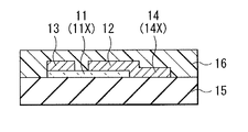
- FIG. 3 is a cross-sectional view of the main part of the touch panel shown in FIG. 2 along the line AA.
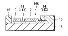
- FIG. 4 is another cross-sectional view taken along line AA of the main part of the touch panel shown in FIG.
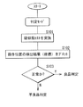
- It is a flowchart for demonstrating the inspection method of determination mode.
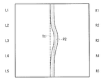
- It is a top view for demonstrating the content of a pseudo finger test (one touch line). It is the figure which plotted the detection result (coordinate) of the operation position at the time of normal. It is the figure which plotted the detection result (coordinate) of the operation position at the time of abnormality.
- FIG. 18 is a cross-sectional view taken along line AA of the main part of the touch panel shown in FIG. It is a top view showing the structure of the touchscreen of a 3rd comparative example. It is a top view for demonstrating the content of a pseudo finger test (three touch lines). It is the figure which plotted the detection result (coordinate) of the operation position.
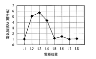
- FIG. 6 is a diagram showing a correlation between electrode positions R1 to R8 and electric resistance RA.
- FIG. 6 is a diagram illustrating a correlation between electrode positions L1 to L8 and an electric resistance RA. It is the figure which plotted the detection result (coordinate) of the operation position after a countermeasure.
- Touch panel first embodiment: two-layer electrode type
- Configuration 1-2 Manufacturing method (including inspection method) 1-3. Action and effect 1-4.
- Modification 2 Touch panel (second embodiment: one-layer electrode type) 2-1.
- Configuration 2-2 Manufacturing method (including inspection method) 2-3. Action and Effect 2-4. Modified example
- Touch panel (first embodiment: two-layer electrode type)> First, the touch panel according to the first embodiment of the present invention will be described.
- the touch panel described here is a so-called capacitive touch panel, and detects an operation position based on a change in capacitance.
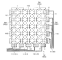
- FIG. 1 schematically shows a planar configuration of the touch panel.
- the touch panel includes a panel unit 10 that is operated with a finger or the like, and a control unit 30 that performs calculation according to a detection result of a change in capacitance generated in the panel unit 10. I have.
- the panel unit 10 includes, for example, a frame 1 and a display panel 2 surrounded by the frame 1. As a result, the panel unit 10 includes the touch area TA1 and the non-touch area TA2 as described above.
- the touch area TA1 is an area where the operation position can be sensed when touching the display panel 2 with a finger or the like to operate the panel unit 10 because the display panel 2 is not shielded by the frame 1.
- the non-touch area TA2 is an area where the operation position cannot be detected when the display panel 2 is touched with a finger or the like.
- the display panel 2 is, for example, one or more of a liquid crystal display panel, an organic electroluminescence (EL) panel, an electronic paper panel, and the like, and may be a panel of a display system other than those.
- EL organic electroluminescence
- the control unit 30 includes, for example, an integrated circuit (IC) and a flexible wiring board (FPC).
- IC integrated circuit
- FPC flexible wiring board
- FIG. 2 shows a planar configuration of the main part of the touch panel shown in FIG.
- FIG. 3 and FIG. 4 represents a cross-sectional configuration along the line AA of the main part shown in FIG.
- a line (dashed line) L shown in FIG. 2 indicates a boundary between the touch area TA1 and the non-touch area TA2. That is, the area inside the line L is the touch area TA1, and the area outside the line L is the non-touch area TA2.
- the touch panel is electrically connected to the transparent electrode 11, the first electrode pad 12 and the second electrode pad 13 provided on the transparent electrode 11, and the transparent electrode 11. Wiring 14 is provided.
- each of the first electrode pad 12 and the second electrode pad 13 is shaded for easy identification.
- the transparent electrode 11 is an electrode having optical transparency, and is used for detecting a change in capacitance (operation position) caused by a touch body (contact object) such as a finger and detecting a displacement of the operation position. It is done.
- the thickness of the transparent electrode 11 is, for example, about 10 nm to about 50 nm.
- the touch panel described here includes a plurality of transparent electrodes 11, and the plurality of transparent electrodes 11 has, for example, a two-layer structure. That is, the touch panel is a two-layer electrode type.
- the plurality of transparent electrodes 11 are arranged in the touch area TA1 and the non-touch area TA2.
- the plurality of transparent electrodes 11 include, for example, a plurality of lower transparent electrodes 11X extending in the horizontal direction and arranged in the vertical direction, and a plurality of layers extending in the vertical direction and arranged in the horizontal direction. And the upper transparent electrode 11Y.
- the non-touch area TA2 is, for example, on the non-touch area TA21 (first non-touch area) located on one side (right side) of the touch area TA1 in the horizontal direction and on the other side (left side) of the touch area TA1 in the horizontal direction. It includes a non-touch area TA22 (second non-touch area) located.
- the lower transparent electrode 11X extends from the non-touch area TA21 to the non-touch area TA22 via the touch area TA1.
- the planar shape of the lower transparent electrode 11X is not particularly limited.
- the lower transparent electrode 11X has, for example, a planar shape in which the wide portions 11M and the narrow portions 11N are alternately connected and the wide portions 11M are disposed at both ends.
- the planar shape of the wide part 11M located at both ends is not particularly limited, for example, it is a trapezoid in which an upper base and a lower base are arranged in the horizontal direction.
- the planar shape of the wide portion 11M located at other than both ends is not particularly limited, but is, for example, a rectangle in which the extending directions of two sides facing each other are inclined with respect to the lateral direction.
- the planar shape of the narrow portion 11N is not particularly limited, but is, for example, a rectangle extending in the horizontal direction.
- the lower transparent electrode 11X includes, for example, one or more of transparent conductive materials having high light transmittance and low electrical resistance.
- the transparent conductive material include a transparent electrode material and metal nanowires.
- a specific example of the transparent electrode material is indium tin oxide (ITO).
- ITO indium tin oxide
- metal nanowires include silver nanowires and copper nanowires.
- the lower transparent electrode 11X including the metal nanowire may further include any one kind or two or more kinds of polymer compounds (so-called binders).
- the kind of the polymer compound is arbitrary.
- metal nanowires are dispersed in the polymer compound, and the metal nanowires are held by the polymer compound.
- the mixing ratio of the metal nanowire and the polymer compound is arbitrary.
- the non-touch area TA2 is, for example, a non-touch area TA23 (first non-touch area) positioned on one side (lower side) of the touch area TA1 in the vertical direction and the other side (upper side) of the touch area TA1 in the vertical direction. And a non-touch area TA24 (second non-touch area) located in the area.
- the upper transparent electrode 11Y extends from the non-touch area TA23 to the non-touch area TA24 via the touch area TA1.
- the configuration and forming material of the upper transparent electrode 11Y are, for example, the same as those of the lower transparent electrode 11X described above.
- the plurality of lower transparent electrodes 11X extending in the horizontal direction and the plurality of upper transparent electrodes 11Y extending in the vertical direction intersect each other.
- the plurality of lower transparent electrodes 11X and the plurality of upper transparent electrodes 11Y are arranged so that the narrow portions 11N overlap each other.
- the first electrode pad 12 is an electrode pad (connection electrode pad) used for connecting the transparent electrode 11 and the wiring 14, and the second electrode pad 13 is used for measuring an electrical resistance RA described later. It is an electrode pad (electrode pad for measurement) used.
- the “electric resistance RA” mainly includes an electric resistance RC of a transparent electrode 11 itself, which will be described later, a contact resistance of the first electrode pad 12 with respect to the transparent electrode pad 11, and a second resistance with respect to the transparent electrode 11. Contact resistance of the electrode pad 13.
- the first electrode pad 12 and the second electrode pad 13 are used as a pair of terminals for resistance measurement.
- the first electrode pad 12 and the second electrode pad 13 are both provided at one end portion of the transparent electrode 11 located in the non-touch area TA2, and are separated (separated) from each other.
- the reason why the first electrode pad 12 and the second electrode pad 13 are arranged in the non-touch area TA2 is to avoid the first electrode pad 12 and the second electrode pad 13 being visually recognized by the operator of the touch panel. is there.
- the lower transparent electrode 11X extends from the non-touch area TA21 to the non-touch area TA22 via the touch area TA1. Therefore, the lower transparent electrode 11X has one end 11X1 located in the non-touch area TA21 and one end 11X2 located in the non-touch area TA22.
- the first electrode pad 12 and the second electrode pad 13 are provided on one of the one end portions 11X1 and 11X2.
- the 1st electrode pad 12 and the 2nd electrode pad 13 are provided in one end 11X1 located in non-touch field TA21, for example.
- the upper transparent electrode 11Y extends from the non-touch area TA23 to the non-touch area TA24 via the touch area TA1. For this reason, the upper transparent electrode 11Y has one end portion 11Y1 located in the non-touch area TA23 and one end portion 11Y2 located in the non-touch area TA24.
- the first electrode pad 12 and the second electrode pad 13 are provided on one of the one end portions 11Y1 and 11Y2.
- the first electrode pad 12 and the second electrode pad 13 are provided, for example, at one end 11Y1 located in the non-touch area TA23.
- the planar shape of the first electrode pad 12 is not particularly limited, but is, for example, a rectangle extending in the vertical direction.
- the planar shape of the second electrode pad 13 is not particularly limited, but is, for example, a rectangle extending in the vertical direction.
- the planar shape of the first electrode pad 12 and the planar shape of the second electrode pad 13 may be the same or different.
- the relationship between the area of the planar shape of the first electrode pad 12 and the area of the planar shape of the second electrode pad 13 is not particularly limited.
- FIG. 2 shows a case where the area of the planar shape of the first electrode pad 12 is larger than the area of the planar shape of the second electrode pad 13.
- the area of the planar shape of the first electrode pad 12 may be smaller than the area of the planar shape of the second electrode pad 13.
- the planar area of the first electrode pad 12 and the planar area of the second electrode pad 13 may be the same.
- each of the first electrode pad 12 and the second electrode pad 13 is provided at the one end portion 11X1.
- the position is not particularly limited.
- the 1st electrode pad 12 and the 2nd electrode pad 13 are provided in one surface (for example, upper surface or lower surface) of lower layer transparent electrode 11X (one end part 11X1).
- the first electrode pad 12 and the second electrode pad 13 are arranged in a plurality of surfaces (upper surface, side surface, and lower surface) of the one end portion 11X1 rather than being arranged on two different surfaces.
- the first electrode pad 12 and the second electrode pad 13 are arranged so as to approach each other on the same surface. This is because a resistance measurement probe (probe pin) is easily brought into contact with each of the first electrode pad 12 and the second electrode pad 13 when measuring the electric resistance RA.
- the positional relationship between the first electrode pad 12 and the second electrode pad 13 is not particularly limited.
- the 1st electrode pad 12 and the 2nd electrode pad 13 are arrange
- the first electrode pad 12 and the second electrode pad 13 are arranged in parallel means that the first electrode pad 12 and the second electrode pad 13 are arranged close to each other so as to be adjacent to each other. means. More specifically, for example, when each of the planar shape of the first electrode pad 12 and the planar shape of the second electrode pad 13 is rectangular, the first electrode is such that the sides facing each other are substantially parallel to each other. A pad 12 and a second electrode pad 13 are disposed.
- the first electrode pads 12 and the second electrode pads 13 are arranged in the vertical direction, for example.
- the details regarding the installation position and positional relationship of the first electrode pad 12 and the second electrode pad 13 provided at the one end 11X1 of the lower transparent electrode 11X are, for example, the first electrode 11Y1 provided at the one end 11Y1 of the upper transparent electrode 11Y. The same applies to the installation position and positional relationship of the first electrode pad 12 and the second electrode pad 13.
- Each of the first electrode pad 12 and the second electrode pad 13 includes, for example, any one type or two or more types of conductive materials having low electrical resistance.
- the conductive material include a metal paste and a carbon paste.
- Specific examples of the metal paste include silver paste and copper paste.
- Each of the first electrode pad 12 and the second electrode pad 13 may be a thin film containing the above-described conductive material.
- the forming material of the first electrode pad 12 and the forming material of the second electrode pad 13 may be the same or different.
- the wiring 14 is disposed in the non-touch area TA2, and is, for example, a so-called signal wiring.
- the reason why the wiring 14 is arranged in the non-touch area TA2 is to prevent the touch panel operator from visually recognizing the wiring 14 like the first electrode pad 12 and the second electrode pad 13 described above. .
- the touch panel described here includes a plurality of wirings 14.
- the plurality of wirings 14 have a two-layer structure, for example, like the plurality of transparent electrodes 11 described above.
- the plurality of wirings 14 include, for example, a plurality of lower layer wirings 14X electrically connected to the plurality of lower layer transparent electrodes 11X and a plurality of upper layer wirings electrically connected to the plurality of upper layer transparent electrodes 11Y. 14Y.
- the plurality of lower-layer wirings 14X are included in the non-touch areas TA21 and TA22. It is arranged in either one.
- the first electrode pad 12 is provided at one end portion 11X1 of the lower transparent electrode 11X located in the non-touch area TA21, the lower wiring 14X is also arranged in the non-touch area TA21.
- the lower layer wiring 14 ⁇ / b> X is connected to the first electrode pad 12. For this reason, the lower layer wiring 14 ⁇ / b> X is electrically connected to the lower layer transparent electrode 11 ⁇ / b> X through the first electrode pad 12. On the other hand, the lower layer wiring 14 ⁇ / b> X is separated from the second electrode pad 13. However, the second electrode pad 13 is electrically connected to the first electrode pad 12 through the lower transparent electrode 11X.
- the lower layer wiring 14X includes, for example, the same conductive material as that of the lower layer transparent electrode 11X.
- the material for forming the lower wiring 14X and the material for forming the lower transparent electrode 11X may be the same or different.
- the plurality of upper-layer wirings 14Y are included in the non-touch areas TA23 and TA24. It is arranged in either one.
- the upper wiring 14Y is also arranged in the non-touch area TA23.
- the upper layer wiring 14Y is connected to the first electrode pad 12. For this reason, the upper layer wiring 14 ⁇ / b> Y is electrically connected to the upper layer transparent electrode 11 ⁇ / b> Y via the first electrode pad 12. On the other hand, the upper layer wiring 14 ⁇ / b> Y is separated from the second electrode pad 13. However, the second electrode pad 13 is electrically connected to the first electrode pad 12 via the upper transparent electrode 11Y.
- the upper layer wiring 14Y includes, for example, the same conductive material as that of the upper layer transparent electrode 11Y.
- the material for forming the upper wiring 14Y and the material for forming the upper transparent electrode 11Y may be the same or different.
- the lower layer wiring 14X is provided so as to be integrated with the first electrode pad 12, for example, as shown in FIG. That is, the first electrode pad 12 and the wiring 14X are formed in the same process. This is because the first electrode pad 12 and the wiring 14X are formed in one process, which simplifies the manufacturing process of the touch panel.
- the upper layer wiring 14Y is provided so as to be integrated with the first electrode pad 12 for the same reason as the lower layer wiring 14X, for example.
- the transparent electrode 11 lower layer transparent electrode 11X
- the first electrode pad 12 the second electrode pad 13
- the wiring 14 lower layer wiring 14X
- the base 15 is not shown.
- the substrate 15 is, for example, one or more of polymer compounds such as polyethylene terephthalate (PET), polycarbonate (PC), polymethyl methacrylate (PMMA) and cycloolefin resin (COP, COC). Is included. This is because the specific gravity of these polymer compounds is smaller than the specific gravity of glass, so that the weight of the touch panel can be reduced.
- PET polyethylene terephthalate
- PC polycarbonate
- PMMA polymethyl methacrylate
- COC cycloolefin resin
- the base 15 may be a rigid substrate or a flexible film.
- the substrate 15 may be a single layer or a multilayer.
- the lower transparent electrode 11X, the first electrode pad 12 and the second electrode pad 13 provided on the lower transparent electrode 11X, and the lower wiring 14X are provided.
- the upper transparent electrode 11Y, the first electrode pad 12 and the second electrode pad 13 provided on the upper transparent electrode 11Y, and the upper wiring 14Y are bonded to the substrate 15.
- the surface of the substrate 15 may be coated with an adhesive 16 such as a double-sided tape.
- an adhesive 16 such as a double-sided tape.
- a needle-like probe is used as a resistance measurement probe. That's fine. That is, a needle-like probe is pierced into the adhesive 16 and the needle-like probe is brought into contact with each of the first electrode pad 12 and the second electrode pad 13.
- an opening 16K may be provided in the adhesive 16, and the first electrode pad 12 and the second electrode pad 13 may be exposed in the opening 16K.
- the degree of freedom regarding the shape of the probe is increased.
- capacitance is generated between the lower transparent electrode 11X and the upper transparent electrode 11Y at the intersection of the lower transparent electrode 11X and the upper transparent electrode 11Y.
- capacitive coupling occurs between the finger or the like and the upper transparent electrode 11Y. Therefore, at the position (operation position) where the finger touches, the electrostatic capacitance described above is generated. The capacity changes. Since the change in capacitance is detected by the control unit 30, the operation position is detected based on the change in capacitance.
- This touch panel is manufactured by the following procedure, for example. Since the touch panel inspection method is a part of the touch panel manufacturing method described here, the touch panel inspection method will also be described below.
- the transparent electrode 11 is formed on the substrate 15 (touch area TA1 and non-touch area TA2).
- the transparent conductive material is patterned to form a plurality of lower transparent electrodes 11X.
- the transparent conductive material is patterned to form a plurality of upper transparent electrodes 11Y.
- the adhesive 16 or the like may be interposed between the lower transparent electrode 11X and the upper transparent electrode 11Y in order to separate the lower transparent electrode 11X and the upper transparent electrode 11Y from each other. .
- the method for depositing the transparent conductive material is not particularly limited, and for example, any one or two or more of a sputtering method, a coating method, a printing method, and the like can be used.
- the patterning method of the transparent conductive material is not particularly limited, but may be one or more of dry etching method and wet etching method.
- the first electrode pad 12 and the second electrode pad 13 are formed at one end of the transparent electrode 11 located in the non-touch area TA2 so as to be separated from each other.
- the conductive material is patterned to form the first electrode pad 12 and the second electrode pad 13. . Further, after depositing a conductive material on the surface of the one end portion 11Y1 of the upper transparent electrode 11Y, the conductive material is patterned to form the first electrode pad 12 and the second electrode pad 13.
- the deposition method and patterning method of the conductive material are the same as, for example, the above-described deposition method and etching method of the transparent conductive material.
- the first electrode pad 12 and the second electrode pad 13 may be formed using a pattern printing technique such as a screen printing method.
- the wiring 14 is formed on the base body 15 (non-touch area TA2).
- the conductive material is patterned to form a plurality of lower layer wirings 14X. Further, after depositing a conductive material on the surface of the substrate 15, the conductive material is patterned to form a plurality of upper layer wirings 14Y.
- a plurality of lower layer wirings 14X and a plurality of upper layer wirings 14Y may be formed using a pattern printing technique such as a screen printing method. Note that, as described above, the adhesive 16 or the like may be interposed between the lower layer wiring 14X and the upper layer wiring 14Y in order to separate the lower layer wiring 14X and the upper layer wiring 14Y from each other.
- the second electrode pad 12 and the second electrode pad 13 formed on the one end portion 11X1 of the lower layer transparent electrode 11X are connected to the first electrode pad 12 and the second electrode pad 12X.
- the electrode pad 13 is separated from the electrode pad 13.
- the second electrode pad 12 and the second electrode pad 13 formed on the one end 11Y1 of the upper transparent electrode 11Y are connected to the first electrode pad 12 and the second electrode pad 12Y.
- the electrode pad 13 is separated from the electrode pad 13.
- the order of forming the transparent electrode 11, the first electrode pad 12, the second electrode pad 13 and the wiring 14 can be arbitrarily changed.
- the first electrode pad 12 and the second electrode pad 13 may be formed in separate steps.
- the first electrode pad 12 and the second electrode pad 13 provided on the one end portion 11X1 of the lower transparent electrode 11X and the lower wiring 14X are formed in one step.
- the conductive material is patterned, and the first electrode pad 12, the second electrode pad 13, and the lower layer wiring 14X are collectively connected.
- the first electrode pad 12 and the lower layer wiring 14X are formed so as to be integrated.
- the first electrode pad 12, the second electrode pad 13, and the lower layer wiring 14X may be collectively formed by using a pattern printing technique such as a screen printing method.
- the first electrode pad 12 and the second electrode pad 13 provided on the one end portion 11Y1 of the upper transparent electrode 11Y and the upper wiring 14Y are formed in one step.
- the conductive material is patterned, and the first electrode pad 12, the second electrode pad 13, and the upper layer wiring 14Y are collectively.
- the first electrode pad 12 and the upper layer wiring 14Y are formed so as to be integrated.
- the first electrode pad 12, the second electrode pad 13, and the upper layer wiring 14Y may be collectively formed by using a pattern printing technique such as a screen printing method.
- the base 15 is made of glass or the like through the adhesive 16. Affixed to a transparent substrate (not shown).
- the lower transparent electrode 11X and the upper transparent electrode 11Y and the like are pasted using the adhesive 16. You may combine them. Specifically, first, the lower transparent electrode 11X, the first electrode pad 12 and the second electrode pad 13 provided on the lower transparent electrode 11X, and the lower wiring 14X are formed on the substrate 15. Subsequently, on a transparent substrate (not shown) such as a glass plate, the upper transparent electrode 11Y, the first electrode pad 12 and the second electrode pad 13 provided on the upper transparent electrode 11Y, and the upper wiring 14Y Form. Finally, the substrate 15 and the transparent substrate are bonded together via the adhesive 16.
- the panel unit 10 (the frame 1 and the display panel 2) is manufactured using the base body 15 on which the transparent electrode 11, the first electrode pad 12, the second electrode pad 13, and the wiring 14 are provided.
- the control unit 30 is connected to the panel unit 10 using an adhesive or the like.
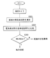
- FIG. 5 shows the flow of the inspection method in the judgment mode.
- FIG. 6 shows a plan configuration of the main part of the touch panel corresponding to FIG. 2 in order to explain the procedure of the pseudo finger test (one touch line).
- FIG. 7 and FIG. 8 is a plot of the detection result (coordinates) of the operation position.
- the wiring 14 is not shown in order to simplify the illustration.
- R1 to R5 and L1 to L5 shown in FIGS. 7 and 8 represent electrode positions. Specifically, the electrode positions R1 to R5 are the rightmost positions of the plurality of lower transparent electrodes 11X shown in FIG. The electrode positions L1 to L5 are the left end positions of the plurality of lower transparent electrodes 11X.
- a pseudo finger test is performed using the touch panel (step S101 in FIG. 5).
- a pseudo finger test is performed using the touch panel (step S101 in FIG. 5).
- the touch panel for example, as shown in FIG. 6, from the upper end to the lower end of the touch area TA ⁇ b> 1 using a pseudo finger along the linear touch line T ⁇ b> 1 drawn in the center area of the touch area TA ⁇ b> 1.
- the display panel 2 (see FIG. 1) is continuously touched.
- the position to be touched is not particularly limited as long as it is one of the touch areas TA1.
- the number of touches that is, the number of touch lines T1 is not particularly limited as long as it is one or more.
- the operation position that is, the detection result (coordinates) of the pseudo finger contact position with respect to the display panel 2 is plotted (step S102 in FIG. 5). Thereby, as shown in FIG. 7 and FIG. 8, plot lines P1 and P2 are obtained.
- the plot line P1 does not have to exactly match the touch line T1.
- a margin may be provided in order to determine whether or not the plot line P1 matches the touch line T1 in consideration of detection errors and the like. Specifically, for example, when the deviation of the plot line P1 from the touch line T1 is 0.5 mm, it may be determined that the plot line P1 matches the touch line T1.
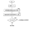
- FIGS. 9 to 11 shows the flow of the inspection method in the analysis mode.
- the inspection method in the analysis mode described here includes, for example, three inspection steps (analysis modes 1 to 3).
- an electrical resistance measuring device such as a tester including a pair of probes for resistance measurement
- one probe is brought into contact with the first electrode pad 12 and the other probe is connected to the second electrode pad. 13 is contacted.
- the electric resistance RA (measured value) is compared with the reference resistance RAS (reference value) (step S202 in FIG. 9).
- the reference resistance RAS is an electrical resistance RA measured when the contact state between the transparent electrode 11, the first electrode pad 12, and the second electrode pad 13 is normal. More specifically, the value of the reference resistor RAS is measured when the detection performance of the operation position is normal because the plot line P1 coincides with the touch line T as shown in FIG. The value of the electrical resistance that should be. This reference resistance RAS is set in advance.
- the electrical resistance RA does not have to exactly match the reference resistance RAS.
- a margin may be provided in order to determine whether or not the electrical resistance RA matches the reference resistance RAS in consideration of measurement errors and the like. Specifically, for example, when the deviation of the electrical resistance RA with respect to the reference resistance RAS is ⁇ 10%, it may be determined that the electrical resistance RA and the reference resistance RAS match.
- the cause may be an abnormal state of the first electrode pad 12 and the second electrode pad 13 (step S203N in FIG. 9).
- This “abnormality of contact state” refers to, for example, damage to the first electrode pad 12, damage to the second electrode pad 13, poor contact of the first electrode pad 12 with the transparent electrode 11, and the second electrode pad 13 with respect to the transparent electrode 11. Such as poor contact.
- measures are taken to repair the touch panel.
- This countermeasure includes, for example, replacement (re-formation) of the first electrode pad 12 and replacement (re-formation) of the second electrode pad 13.
- the electrical resistance RA is set using all the first electrode pads 12 and all the second electrode pads 13 among the plurality of first electrode pads 12 and the plurality of second electrode pads 13.
- the electrical resistance RA may be measured using some of the first electrode pads 12 and some of the second electrode pads 13.
- the occurrence of a defect is based on the result of the pseudo finger test (plot shown in FIG. 8) performed in the determination mode. It is preferable to anticipate the first electrode pad 12 and the second electrode pad 13 that are the cause.
- the plot line P2 greatly deviates from the touch line T1 particularly at the electrode positions R3 and L3, and the plot line P2 at the electrode positions R2, R4, L2 and L4. Is slightly out of touch line T1.
- the first electrode pads R3 and L3 located at the electrode positions R3 and L3 are used.
- the electrical resistance RA is measured using the electrode pad 12 and the second electrode pad 13.
- the first electrode pad 12 and the second electrode pad 13 positioned at the electrode positions R3 and L3 are the cause of the detection failure
- the electrical resistance RA may be measured using the first electrode pad 12 and the second electrode pad 13 located at the electrode positions R2 and L2, or the first position located at the electrode positions R4 and L4.
- the electrical resistance RA may be measured using the electrode pad 12 and the second electrode pad 13.
- step S203Y in FIG. 9 If the cause of the detection failure is another cause (step S203Y in FIG. 9), then it is examined whether or not the state of the wiring 14 is abnormal (analysis mode 2). In this case, the electrical resistance RB of the wiring 14 is measured using an electrical resistance measuring device such as a tester (step S301 in FIG. 10).
- the electric resistance RB (measured value) is compared with the reference resistance RBS (reference value) (step S302 in FIG. 10).
- This reference resistance RBS is an electrical resistance RB that is measured when the state of the wiring 14 is normal, like the above-described reference resistance RAS, and is set in advance.
- step S303 in FIG. 10 it is determined whether or not the electrical resistance RB matches the reference resistance RBS.
- the electrical resistance RB matches the reference resistance RBS, it is determined that the cause of the detection failure is other than the wiring 14 because there is no abnormality in the state of the wiring 14 (step S303Y in FIG. 10). It should be noted that, as with the case described with respect to the electrical resistance RA and the reference resistance RAS, if the margin is used, the electrical resistance RB may not exactly match the reference resistance RBS.
- Step S303N This “abnormal state of the wiring 14” is, for example, disconnection of the wiring 14 or the like. In this case, measures are taken to repair the touch panel. This measure is, for example, replacement (re-formation) of the wiring 14 or the like.
- the electrical resistances RB of all the wirings 14 may be measured, or the electrical resistances RB of some of the wirings 14 are measured. May be.
- the detection failure is detected based on the result of the pseudo finger test (plot shown in FIG. 8). It is preferable to measure the electrical resistance RB of the wiring 14 after predicting the wiring 14 that is the cause of the occurrence.
- step S303Y in FIG. 10 If the cause of the detection failure is another cause (step S303Y in FIG. 10), then it is examined whether or not the state of the transparent electrode 11 is normal (analysis mode 3). In this case, the electrical resistance RC of the transparent electrode 11 is measured using an electrical resistance measuring device such as a tester (step S401 in FIG. 11).
- an electrical resistance measuring device such as a tester
- one probe is brought into contact with the first electrode pad 12 arranged in the non-touch area TA21 out of a pair of resistance measurement probes. At the same time, the other probe is brought into contact with one end 11X2 arranged in the non-touch area TA22.
- one probe When measuring the electrical resistance RC of the upper transparent electrode 11Y, for example, one probe is brought into contact with the first electrode pad 12 arranged in the non-touch area TA23 and arranged in the non-touch area TA24. The other probe is brought into contact with the one end portion 11Y2.
- the electric resistance RC (measured value) is compared with the reference resistance RCS (reference value) (step S402 in FIG. 11).
- This reference resistance RCS is an electrical resistance RC measured when the state of the transparent electrode 11 is normal, like the reference resistance RAS described above, and is set in advance.
- the electrical resistance RC matches the reference resistance RCS, the state of the transparent electrode 11 is not abnormal, so it is determined that the cause of the detection failure is a cause other than the transparent electrode 11 (step S403Y in FIG. 11). It should be noted that, as long as a margin is used, the electrical resistance RC may not exactly match the reference resistance RCS, as in the case described with respect to the electrical resistance RA and the reference resistance RAS.
- the electrical resistance RC does not match the reference resistance RCS, it is determined that there is a possibility that the cause of the detection failure is the state abnormality of the transparent electrode 11 because the state of the transparent electrode 11 is abnormal (see FIG. 11 step S403N).
- This “abnormal state of the transparent electrode 11” is, for example, damage or deterioration of the transparent electrode 11.
- measures are taken to repair the touch panel.
- This countermeasure is, for example, replacement (re-formation) of the transparent electrode 11 or the like.
- the electrical resistance RC of all the transparent electrodes 11 may be measured, or the electrical resistance RC of some of the transparent electrodes 11 is measured. May be measured.
- the detection failure is based on the result of the pseudo finger test (plot shown in FIG. 8). It is preferable to measure the electrical resistance RC of the transparent electrode 11 after predicting the transparent electrode 11 that is the cause of the occurrence of this.
- the state of the transparent electrode 11 is observed using a microscope or the like.
- the transparent electrode 11 is transparent. It is determined that no abnormality has occurred in the state of the electrode 11.
- the wiring 14 (lower layer wiring 14X, upper layer wiring 14Y) is connected to one end portions 11X1, 11Y1 of the transparent electrode 11 (lower layer transparent electrode 11X and upper layer transparent electrode 11Y) located in the non-touch area TA2.
- a connected first electrode pad 12 and a second electrode pad 13 spaced from the first electrode pad 12 and the wiring 14 are provided. Therefore, it is possible to easily and accurately identify the cause of the operation position detection failure for the reason described below.
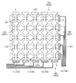
- FIG. 12 represents the configuration of the touch panel of the first comparative example (planar configuration corresponding to FIG. 2)
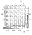
- FIG. 13 represents the configuration of the touch panel of the second comparative example (planar configuration corresponding to FIG. 2). ing.
- the touch panel of the first comparative example is such that only the first electrode pad 12 is provided at one end 11X1, 11Y1 of the transparent electrode 11 (the lower transparent electrode 11X and the upper transparent electrode 11Y). Except for this, it has the same configuration as the touch panel of this embodiment.
- the touch panel of the second comparative example is provided with the first electrode pad 12 at one end portions 11X1 and 11Y1 of the transparent electrode 11 (the lower transparent electrode 11X and the upper transparent electrode 11Y).
- the touch panel has the same configuration as that of the touch panel of the present embodiment except that the second electrode pad 13 is provided at one end 11X2 and 11Y2 opposite to the one end 11X1 and 11Y1.
- the second electrode pad 13, that is, another electrode pad separated from the first electrode pad 12 is not provided on the transparent electrode 11. .
- the thickness of the transparent electrode 11 is thin and the strength of the transparent electrode 11 is weak, it is difficult to directly measure the electric resistance RC of the transparent electrode 11, and only the first electrode pad 12 is used. This is because it is practically difficult to measure the electric resistance RA. For this reason, even if an abnormality occurs in the contact state of the first electrode pad 12 with respect to the transparent electrode 11, it is easy and accurate that the cause of the defective detection of the operation position is an abnormality in the contact state of the first electrode pad 12. It is difficult to specify.
- the transparent electrode 11 is provided with the second electrode pad 13 together with the first electrode pad 12, the first electrode pad 12 and the second electrode pad 13 are connected to a pair of terminals for resistance measurement. Can be used to measure the electrical resistance RA.
- the first electrode pad 12 is provided at one end 11X1, 11Y1, whereas the second electrode pad 13 is provided at one end 11X2, 11Y2 opposite to the one end 11X1, 11Y1. Therefore, the first electrode pad 12 and the second electrode pad 13 are greatly separated via the transparent electrode 11.
- the electric resistance of the transparent electrode 11 is larger than the electric resistance of the first electrode pad 12 and the electric resistance of the second electrode pad 13, the electric resistance of the transparent electrode 11 has a great influence on the electric resistance RA. Therefore, it is difficult to accurately measure the electric resistance RA. Such a tendency that it is difficult to accurately measure the electric resistance RA becomes particularly remarkable as the electric resistance of the transparent electrode 11 is increased.
- the first cause is that the influence of the electrical resistance of the transparent electrode 11 on the electrical resistance RA is large even though the contact state of the first electrode pad 12 and the second electrode pad 13 with respect to the transparent electrode 11 does not occur. This is a case where the electrical resistance RA becomes large.
- the second cause is a case where the electrical resistance RA increases because of an abnormality in the contact state of the first electrode pad 12 and the second electrode pad 13 with respect to the transparent electrode 11.
- the cause of the defective detection of the operation position is the cause of the first electrode pad 12 and the second electrode pad 13. It is difficult to easily and accurately specify that the contact state is abnormal.
- both the first electrode pad 12 and the second electrode pad 13 are provided at the one end portions 11X1 and 11Y1, the first electrode pad 12 and the second electrode pad 13 Is approaching through the transparent electrode 11.
- the electric resistance of the transparent electrode 11 is larger than the electric resistance of the first electrode pad 12 and the electric resistance of the second electrode pad 13, the influence of the electric resistance of the transparent electrode 11 on the electric resistance RA is small. Therefore, it becomes easy to accurately measure the electric resistance RA.
- the cause of the operation position detection failure is the first even without using the control unit 30. It is possible to easily and accurately specify that the contact state between the electrode pad 12 and the second electrode pad 13 is abnormal.
- the first electrode pad 12 and the second electrode pad 13 are provided on one surface of the transparent electrode 11, the first electrode pad 12 and the second electrode pad 13 are used for resistance measurement. Since it becomes easy to make a probe contact, a higher effect can be acquired. In this case, if the first electrode pad 12 and the second electrode pad 13 are arranged in parallel, it becomes easier to bring the resistance measurement probe into contact with the first electrode pad 12 and the second electrode pad 13. Even higher effects can be obtained.
- the first electrode pad 12 and the wiring 14 are provided so as to be integrated, the first electrode pad 12 and the wiring 14 are formed in one step.
- the touch panel manufacturing process can be simplified.
- the first electrode pad 12 provided at one end portions 11X1 and 11Y1 of the transparent electrode 11 located in the non-touch area TA2 and connected to the wiring 14.
- the second electrode pad 13 provided at one end 11X1 and 11Y1 of the transparent electrode 11 and spaced from the first electrode pad 12 and the wiring 14, and the electrical resistance RA is measured. Therefore, for the same reason as the touch panel of the present embodiment described above, it is possible to easily and accurately identify the cause of the operation position detection failure.
- the electric resistance RA is compared with the reference resistance RAS.
- the contact failure is improved by implementing the above measures.
- the cause of the defective detection of the operation position can be specified only by measuring the electric resistance RA and comparing the electric resistance RA with the reference resistance RAS. That is, in addition to measuring the electrical resistance RA, the cause of the operation position detection failure can be identified without measuring the electrical resistance RB of the wiring 14 and the electrical resistance RC of the transparent electrode 11. Therefore, when a defective touch panel is generated, it takes less time to specify the cause of the operation position detection failure, so that the cause can be quickly identified. Along with this, measures such as repair can be executed at an early stage so that a defective touch panel becomes a non-defective product.
- the first electrode pads 12 and the second electrode pads 13 may be arranged in the lateral direction on one surface of the lower transparent electrode 11X (one end portion 11X1).
- the first electrode pad 12 and the second electrode pad 13 are preferably arranged in parallel. Even in this case, since the resistance measurement probe is easily brought into contact with the first electrode pad 12 and the second electrode pad 13, the first electrode pad 12 and the second electrode pad 13 are arranged in the vertical direction (FIG. 2)).
- Modification 1 regarding the arrangement direction of the first electrode pad 12 and the second electrode pad 13 provided on the lower transparent electrode 11X (one end 11X1) is the first electrode provided on the upper transparent electrode 11Y (one end 11Y1).
- the present invention can also be applied to the arrangement direction of the pad 12 and the second electrode pad 13. In this case, the same effect can be obtained.
- the extending direction of the first electrode pad 12 and the extending direction of the second electrode pad 13 may be different.
- the first electrode pad 12 and the second electrode pad 13 provided in the lower transparent electrode 11X the first electrode pad 12 extends in the vertical direction, whereas the second electrode pad 13 Extends laterally.
- the first electrode pad 12 extends in the lateral direction, whereas the second electrode pad 13 It extends in the vertical direction.
- the resistance measurement probe is easily brought into contact with the first electrode pad 12 and the second electrode pad 13, the first electrode pad 12 and the second electrode pad 13 are arranged in the vertical direction (FIG. 2)).
- the first electrode pad 12 and the second electrode pad 13 may not be provided on one surface of the lower transparent electrode 11X (one end portion 11X1).
- the first electrode pad 12 is provided on one surface (for example, the upper surface) of the lower transparent electrode 11X
- the second electrode pad 13 is provided on the other surface of the lower transparent electrode 11X (for example, the upper surface) It may be provided on the lower surface.
- the first electrode pad 12 and the second electrode pad 13 are formed of the lower transparent electrode 11X. It is preferable to be provided on one surface of (one end portion 11X1).
- the first electrode pad 12 and the second electrode pad 13 do not have to be provided on one surface. The same applies to the first electrode pad 12 and the second electrode pad 13 provided on the upper transparent electrode 11Y. is there.
- the first electrode pad 12 and the lower layer wiring 14 ⁇ / b> X may be provided separately. That is, the first electrode pad 12 and the lower layer wiring 14X may be formed in separate steps. In this case, since the forming material of the first electrode pad 12 and the forming material of the lower layer wiring 14X can be made different, the degree of freedom regarding the forming material of the first electrode pad 12 and the forming material of the lower layer wiring 14X is expanded. In FIG. 16, illustration of the adhesive 16 is omitted.
- first electrode pad 12 and the upper layer wiring 14Y may be provided separately.
- touch panel manufacturing method and inspection method described above can be changed as appropriate, as exemplified below.
- the analysis mode 3 is inspected first to determine whether or not the state of the transparent electrode 11 is normal, and then the analysis mode 2 is inspected to determine the state of the wiring 14. It may be determined whether or not there is any abnormality. Even in this case, since the inspection in the analysis mode 1 is performed before the inspection in the analysis modes 2 and 3, the same effect can be obtained.
- Touch panel (second embodiment: one-layer electrode type)> Next, a touch panel according to a second embodiment of the present invention will be described. In the following description, the components of the first embodiment already described are referred to as needed.
- FIG. 17 shows a planar configuration of the main part of the touch panel, and corresponds to FIG.
- FIG. 18 shows a cross-sectional configuration along the AA line of the main part shown in FIG. 17, and corresponds to FIG.
- the first electrode pad 18 and the second electrode pad 19 are shaded for easy identification.
- the touch panel of the present embodiment replaces the transparent electrode 11, the first electrode pad 12, the second electrode pad 13, and the wiring 14 with the transparent electrode 17, the first electrode pad 18, Except that the second electrode pad 19 and the wiring 20 are provided, the touch panel has the same configuration as the touch panel of the first embodiment.
- the transparent electrode 17 described here includes a plurality of transparent electrodes 17, and the plurality of transparent electrodes 17 has, for example, a single-layer structure. That is, the touch panel is a one-layer electrode type.
- the transparent electrode 17 is disposed in the touch area TA1 and the non-touch area TA2.
- the plurality of transparent electrodes 17 include, for example, a plurality of right transparent electrodes 17R extending in the horizontal direction and a plurality of left transparent electrodes 17L extending in the horizontal direction.
- the plurality of right transparent electrodes 17R and the plurality of left transparent electrodes 17L are arranged in the vertical direction and are alternately arranged.
- the right transparent electrode 17R mainly extends from the non-touch area TA2 (TA21) to the touch area TA1.
- the planar shape of the right transparent electrode 17R is not particularly limited, but is, for example, a right triangle.
- the width of the right transparent electrode 17R gradually decreases from the non-touch area TA21 toward the touch area TA1.
- the left transparent electrode 17L mainly extends from the non-touch area TA2 (TA22) to the touch area TA1.
- the planar shape of the left transparent electrode 17L is not particularly limited, but is, for example, a right triangle.
- the width of the left transparent electrode 17L gradually decreases from the non-touch area TA22 toward the touch area TA1.
- the right transparent electrode 17R and the left transparent electrode 17L adjacent to each other are arranged so that the hypotenuses face each other, for example.
- the distance between the right transparent electrode 17R and the left transparent electrode 17L is, for example, substantially uniform regardless of the position.
- the planar shape of the right transparent electrode 17R and the planar shape of the left transparent electrode 17L are other than a right triangle.
- Other shapes may be used.
- the other shape is, for example, a rectangle. Note that the planar shape of the right transparent electrode 17R and the planar shape of the left transparent electrode 17L may be the same or different.
- the configurations of the right transparent electrode 17R and the left transparent electrode 17L other than those described above are the same as the configurations of the lower transparent electrode 11X and the upper transparent electrode 11Y, for example.
- the first electrode pad 18 and the second electrode pad 19 are both provided at one end of the transparent electrode 17 arranged in the non-touch area TA2, and are separated from each other.
- the right transparent electrode 17R extends from the non-touch area TA21 to the touch area TA1. For this reason, the right transparent electrode 17R has a wide end portion 17R1 located in the non-touch area TA21 and a sharp end portion 17R2 located in the touch area TA1. In this case, the first electrode pad 18 and the second electrode pad 19 are provided at the one end portion 17R1.
- the left transparent electrode 17L extends from the non-touch area TA22 to the touch area TA1. For this reason, the left transparent electrode 17L has a wide end 17L1 located in the non-touch area TA22 and a sharp one end 17L2 located in the touch area TA1. In this case, the first electrode pad 18 and the second electrode pad 19 are provided at the one end portion 17L1.
- FIG. 18 shows a case where, for example, the first electrode pad 18 and the wiring 20 are provided so as to be integrated.
- the wiring 20 is disposed in the non-touch area TA2.
- the touch panel described here includes a plurality of wirings 20, and the plurality of wirings 20 have a single-layer structure, for example, like the plurality of transparent electrodes 17 described above.
- the plurality of wirings 20 include, for example, a plurality of right wirings 20R electrically connected to the plurality of right transparent electrodes 17R and a plurality of left wirings electrically connected to the plurality of left transparent electrodes 17L. 20L.
- the right wiring 20R is also arranged in the non-touch area TA21.
- the right wiring 20R is connected to the first electrode pad 18. For this reason, the right wiring 20 ⁇ / b> R is electrically connected to the right transparent electrode 17 ⁇ / b> R via the first electrode pad 18. On the other hand, the right wiring 20 ⁇ / b> R is separated from the second electrode pad 19. However, the second electrode pad 19 is electrically connected to the first electrode pad 18 via the right transparent electrode 17R.
- the left wiring 20L is also arranged in the non-touch area TA22.
- the left wiring 20L is connected to the first electrode pad 18. For this reason, the left wiring 20L is electrically connected to the left transparent electrode 17L via the first electrode pad 18. On the other hand, the left wiring 20 ⁇ / b> L is separated from the second electrode pad 19. However, the second electrode pad 19 is electrically connected to the first electrode pad 18 through the left transparent electrode 17L.
- the configurations of the right side wiring 20R and the left side wiring 20L other than the above are the same as the configurations of the lower layer wiring 14X and the upper layer wiring 14Y, for example.
- a capacitance is generated between the adjacent right transparent electrode 17R and the left transparent electrode 17L.
- the capacitance described above changes at a position (operation position) where the finger touches. Since the change in capacitance is detected by the control unit 30, the operation position is detected based on the change in capacitance.
- a transparent electrode 17, a first electrode pad 18, a second electrode pad 19 and a wiring 20 are formed instead of the transparent electrode 11, the first electrode pad 12, the second electrode pad 13 and the wiring 14. Is manufactured in the same procedure as the touch panel of the first embodiment.
- the transparent electrode 17 is formed on the base 15 (touch area TA1 and non-touch area TA2).
- the transparent conductive material is patterned to form a plurality of right transparent electrodes 17R and a plurality of left transparent electrodes 17L. Details regarding each of the transparent conductive material deposition method and the patterning method are the same as in the first embodiment, for example.
- the first electrode pad 18 and the second electrode pad 19 are formed at one end of the transparent electrode 17 disposed in the non-touch area TA2 so as to be separated from each other.
- the conductive material is patterned to form a plurality of second electrodes.
- One electrode pad 18 and a plurality of second electrode pads 19 are formed. Details regarding each of the conductive material deposition method and the patterning method are the same as in the first embodiment, for example.
- the first electrode pad 18 and the second electrode pad 19 may be formed using a pattern printing technique such as a screen printing method.
- the wiring 20 is formed on the base body 15 (non-touch area TA2).
- the transparent conductive material is patterned to form a plurality of right wirings 20R and a plurality of left wirings 20L.
- the right wiring 20R and the left wiring 20L may be formed using a pattern printing technique such as a screen printing method.
- the right wiring 20R when the right wiring 20R is formed, the right wiring 20R is connected to the first electrode pad 18 among the first electrode pad 18 and the second electrode pad 19 provided in the one end portion 17R1 of the right transparent electrode 17R. In addition, the right wiring 20 ⁇ / b> R is separated from the second electrode pad 19.
- the left wiring 20L When the left wiring 20L is formed, the left wiring 20L is connected to the first electrode pad 18 among the first electrode pad 18 and the second electrode pad 19 provided at the one end portion 17L1 of the left transparent electrode 17L. In addition, the left wiring 20L is separated from the second electrode pad 19.
- the first electrode pad 18 and the second electrode pad 19 provided at the one end portion 17R1 of the right transparent electrode 17R, and the first electrode pad 18 and the second electrode pad provided at the one end portion 17L1 of the left transparent electrode 17L. 19, the right wiring 20R, and the left wiring 20L are formed in one step.
- the conductive material is patterned to form the first electrode pad 18, the second electrode pad 19, and the right wiring 20R.
- the left wiring 20L is formed in a lump.
- the first electrode pad 18 and the right wiring 20R are formed so as to be integrated, and the first electrode pad 18 and the left wiring 20L are formed so as to be integrated.
- R1 to R5 and L1 to L5 shown in FIG. 17 represent electrode positions. Specifically, the electrode positions R1 to R5 are the right end positions of the plurality of right transparent electrodes 17R. The electrode positions L1 to L5 are the left end positions of the plurality of left transparent electrodes 11L.
- a pseudo finger test is performed using the touch panel (step S101 in FIG. 5).
- the upper end of the touch area TA ⁇ b> 1 is used with a pseudo finger along a linear touch line T ⁇ b> 1 drawn in the center area of the touch area TA ⁇ b> 1.
- the display panel 2 (see FIG. 1) is continuously touched from the bottom to the bottom.
- the operation position that is, the detection result (coordinates) of the pseudo finger contact position with respect to the display panel 2 is plotted (step S102 in FIG. 5). Thereby, as shown in FIG. 7 and FIG. 8, plot lines P1 and P2 are obtained.
- an electrical resistance measuring device such as a tester provided with a pair of resistance measuring probes
- the electric resistance RA (measured value) is compared with the reference resistance RAS (reference value) (step S202 in FIG. 9).
- the reference resistance RAS is an electrical resistance RA measured when the contact state between the transparent electrode 17, the first electrode pad 18, and the second electrode pad 19 is normal, and is set in advance.
- a margin may be provided in order to determine whether or not the electrical resistance RA matches the reference resistance RAS in consideration of measurement errors and the like.
- an abnormality has occurred in the contact state of the first electrode pad 18 and the second electrode pad 19 with respect to the transparent electrode 17, so that an operation position detection failure has occurred. It is determined that the cause may be an abnormal state of the first electrode pad 18 and the second electrode pad 19 (step S203N in FIG. 9).
- This “abnormality of contact state” refers to, for example, damage to the first electrode pad 18, damage to the second electrode pad 19, poor contact of the first electrode pad 18 with the transparent electrode 17, and the second electrode pad 19 with respect to the transparent electrode 17. Such as poor contact.
- measures are taken to repair the touch panel.
- This countermeasure includes, for example, replacement (re-formation) of the first electrode pad 18 and replacement (re-formation) of the second electrode pad 19.
- the electrical resistance RA is set using all the first electrode pads 18 and all the second electrode pads 19 among the plurality of first electrode pads 18 and the plurality of second electrode pads 19.
- the electrical resistance RA may be measured using some of the first electrode pads 18 and some of the second electrode pads 19.
- the result of the pseudo finger test performed in the determination mode plot shown in FIG. 8 Based on the above, it is preferable to predict the first electrode pad 18 and the second electrode pad 19 that are the cause of the occurrence of defects.
- step S203Y in FIG. 9 If the cause of the detection failure is another cause (step S203Y in FIG. 9), then it is examined whether or not the state of the wiring 20 is abnormal (analysis mode 2). In this case, the electrical resistance RB of the wiring 20 is measured using an electrical resistance measuring device such as a tester (step S301 in FIG. 10).
- the electric resistance RB (measured value) is compared with the reference resistance RBS (reference value) (step S302 in FIG. 10).
- This reference resistance RBS is an electrical resistance RB measured when the state of the wiring 20 is normal, as with the above-described reference resistance RAS, and is set in advance.
- step S303 in FIG. 10 it is determined whether or not the electrical resistance RB matches the reference resistance RBS.
- the electrical resistance RB matches the reference resistance RBS, it is determined that the cause of the detection failure is other than the wiring 20 because there is no abnormality in the state of the wiring 20 (step S303Y in FIG. 10). It should be noted that, as with the case described with respect to the electrical resistance RA and the reference resistance RAS, if the margin is used, the electrical resistance RB may not exactly match the reference resistance RBS.
- Step S303N This “abnormal state of the wiring 20” is, for example, disconnection of the wiring 20 or the like. In this case, measures are taken to repair the touch panel. This countermeasure is, for example, replacement (re-formation) of the wiring 20 or the like.
- the electrical resistances RB of all the wirings 20 may be measured, or the electrical resistances RB of some of the wirings 20 are measured. May be. Of course, in the latter case, it is preferable to predict the wiring 20 that is the cause of the detection failure based on the result of the pseudo finger test (plot shown in FIG. 8).
- step S303Y in FIG. 10 If the cause of the detection failure is another cause (step S303Y in FIG. 10), then it is examined whether or not the state of the transparent electrode 17 is abnormal (analysis mode 3). In this case, the electrical resistance RC of the transparent electrode 17 is measured using an electrical resistance measuring device such as a tester (step S401 in FIG. 11).
- the electric resistance RC (measured value) is compared with the reference resistance RCS (reference value) (step S402 in FIG. 11).
- This reference resistance RCS is an electrical resistance RC measured when the state of the transparent electrode 11 is normal, like the reference resistance RAS described above, and is set in advance.
- the electrical resistance RC matches the reference resistance RCS, the state of the transparent electrode 17 is not abnormal, and it is determined that the cause of the detection failure is other than the transparent electrode 17 (step S403Y in FIG. 11). It should be noted that, as long as a margin is used, the electrical resistance RC may not exactly match the reference resistance RCS, as in the case described with respect to the electrical resistance RA and the reference resistance RAS.
- the state of the transparent electrode 17 is abnormal, so that it is determined that the cause of the detection failure may be the state of the transparent electrode 17 (see FIG. 11 step S403N).
- This “abnormal state of the transparent electrode 17” is, for example, damage or deterioration of the transparent electrode 17.
- measures are taken to repair the touch panel. This measure is, for example, replacement (re-formation) of the transparent electrode 17 or the like.
- the electrical resistance RC of all the transparent electrodes 17 may be measured, or the electrical resistance RC of some of the transparent electrodes 17 may be measured. May be measured. Of course, in the latter case, it is preferable to predict the transparent electrode 17 that is the cause of the detection failure based on the result of the pseudo finger test (plot shown in FIG. 8).
- the wiring 20 (the right wiring 20R and the left wiring 20L) is connected to the one end portions 17R1, 17L1 of the transparent electrode 17 (the right transparent electrode 17R and the left transparent electrode 17L) located in the non-touch area TA2.
- a connected first electrode pad 18 and a second electrode pad 19 spaced from the first electrode pad 18 and the wiring 20 are provided. Therefore, it is possible to easily and accurately identify the cause of the operation position detection failure for the reason described below.
- FIG. 19 shows the configuration of the touch panel of the third comparative example (planar configuration corresponding to FIG. 17).
- the touch panel of the third comparative example is the touch panel of the present embodiment except that only the first electrode pad 18 is provided at one end portions 17R1, 17L1 of the transparent electrode 17 (the right transparent electrode 17R and the left transparent electrode 17L). It has the same composition as.
- the one end portion 17R2 opposite to the wide end portion 17R1 is sharp, and the first electrode pad 18 is formed on the one end portion 17R2. It is difficult to provide the second electrode pad 19. Thus, it is difficult to provide the first electrode pad 18 and the second electrode pad 19 as well with respect to the one end portion 17L2 on the side opposite to the one end portion 17L1.
- the second electrode pad 19 spaced from the first electrode pad 18 is not provided on the transparent electrode 17, so the first comparative example shown in FIG.
- the touch panel of this embodiment since both the first electrode pad 18 and the second electrode pad 19 are provided at the one end portions 17R1 and 17L1, the touch panel of the first embodiment shown in FIG. For the same reason, it is easy to accurately measure the electric resistance RA. Therefore, when an abnormality occurs in the contact state of the first electrode pad 18 and the second electrode pad 19 with respect to the transparent electrode 17, the cause of the operation position detection failure is the first without using the control unit 30. It is possible to easily and accurately specify that the contact state between the electrode pad 18 and the second electrode pad 19 is abnormal.
- the first electrode pad 18 provided at the one end portions 17R1 and 17L1 of the transparent electrode 17 located in the non-touch area TA2 and connected to the wiring 20.
- the electrical resistance RA is measured using the first electrode pad 18 and the second electrode pad 19 provided at the one end portions 17R1 and 17L1 and separated from the wiring 20. Therefore, for the same reason as the touch panel of the present embodiment described above, it is possible to easily and accurately identify the cause of the operation position detection failure.
- a transparent conductive material ITO was deposited on one surface (touch area TA1 and non-touch area TA2) of the substrate 15 (PET substrate) by using a sputtering method. Then, the transparent conductive material was patterned using the wet etching method, and the transparent electrode 17 (the right side transparent electrode 17R and the left side transparent electrode 17L) was formed. In this case, the number of each of the right transparent electrode 17R and the left transparent electrode 17L was eight, and the thickness of each of the right transparent electrode 17R and the left transparent electrode 17L was 20 nm.
- a conductive material (silver paste) is pattern-printed on the non-touch area TA2 using a screen printing method, and the first electrode pad 18, the second electrode pad 19, and the wiring 20 (the right wiring 20R and the left wiring 20L).
- the first electrode pad 18 provided on the one end portion 17R1 and the right wiring 20R are integrally formed, and the first electrode pad 18 provided on the one end portion 17L1 and the left wiring 20L are integrated. It was formed to become.
- the thickness of each of the first electrode pad 18 and the second electrode pad 19 is 6 ⁇ m
- the thickness of each of the right wiring 20R and the left wiring 20L is 6 ⁇ m.
- an adhesive 16 double-sided tape
- the substrate 15 was attached to a transparent substrate (glass plate).
- the panel unit 10 (the frame 1 and the display panel 2) was manufactured using the substrate 15 attached to the transparent substrate, and then the touch panel was assembled using the control unit 30 and the like together with the panel unit 10.
- FIG. 20 shows a planar configuration of the main part of the touch panel corresponding to FIG. 17 in order to explain the contents of the pseudo finger test (three touch lines).
- FIG. 21 is a plot of operation position detection results (coordinates).
- electrode positions R1 to R8 represent the right end positions of the eight right transparent electrodes 17R
- electrode positions L1 to L8 represent the left end positions of the eight left transparent electrodes 17L.
- a pseudo finger test was performed using three linear touch lines T2 to T4 as shown in FIG.
- the display panel 2 is continuously touched from the upper end to the lower end of the touch area TA1 along the touch line T2 in the left area, the touch line T3 in the central area, and the touch line T4 in the right area. did.
- the plot line P2 deviates from the touch line T2 mainly in the vicinity of the electrode positions R2 to R4 and L2 to L4.
- the plot line P3 deviates from the touch line T2 mainly in the vicinity of the electrode positions R1 to R4 and L1 to L4.
- the plot line P4 deviates from the touch line T2 mainly in the vicinity of the electrode positions R1 to R3 and L1 to L3.
- the operation position detection performance was found to be abnormal.
- the cause of the operation position detection failure is a contact failure between the transparent electrode 17 and the first electrode pad 18 and the second electrode pad 19, the location where the contact failure has occurred,
- the first electrode pad 18 and the second electrode pad 19 can be predicted.
- an abnormality occurs in the contact state between the first electrode pad 18 and the second electrode pad 19 located at the electrode positions R2 and R3. It is expected that Further, it is expected that an abnormality has occurred in the contact state between the first electrode pad 18 and the second electrode pad 19 located at the electrode positions L2 to L4.
- the electrical resistance RA was measured using the first electrode pad 18 and the second electrode pad 19, and then the electrical resistance RA was compared with the reference resistance RAS.
- the electrical resistance RA of the right transparent electrode 17R, the first electrode pad 18 and the second electrode pad 19 is measured, and the left transparent electrode 17L, the first electrode pad 18 and the second electrode are measured.
- the electrical resistance RA of the pad 19 was measured.
- FIG. 22 shows the correlation between the electrode positions R1 to R8 and the electric resistance RA
- FIG. 23 shows the correlation between the electrode positions L1 to L8 and the electric resistance RA.
- the electric resistance RA a value normalized by setting the reference resistance RAS to 1 is shown.
- the electric resistance RA was significantly larger than 1 mainly at the electrode positions R1 and R2. Further, in the correlation between the electrode positions L1 to L8 and the electric resistance RA, as shown in FIG. 23, the electric resistance RA is significantly larger than 1 mainly at the electrode positions L2 to L4. From this result, it is considered that the contact state of the first electrode pad 18 and the second electrode pad 19 located at the electrode positions R1, R2, L2 to L4 is abnormal.
- FIG. 24 is a plot of the operation position detection results (coordinates) after the above countermeasures.
- the plot line P2 coincides with the touch line T2
- the plot line P3 coincides with the touch line T3
- the plot line P4 coincides with the touch line T4. That is, since the cause of the abnormality in the operation position detection performance has been eliminated, the operation position detection performance has been restored to normal.
- the first electrode pad 18 provided at one end 17R1, 17L1 of the transparent electrode 17 located in the non-touch area TA2 and connected to the wiring 20, and the one end 17R1. , 17L1, and the first electrode pad 18 and the second electrode pad 19 separated from the wiring 20 are used to measure the electrical resistance RA, thereby easily and accurately identifying the cause of the operation position detection failure. did it. As a result, the cause of the defective detection of the operation position could be quickly resolved, so that the defective product could be quickly recovered so as to become a non-defective product.
Landscapes
- Engineering & Computer Science (AREA)
- General Engineering & Computer Science (AREA)
- Theoretical Computer Science (AREA)
- Human Computer Interaction (AREA)
- Physics & Mathematics (AREA)
- General Physics & Mathematics (AREA)
- Position Input By Displaying (AREA)
Abstract
タッチパネルは、タッチ領域および非タッチ領域に配置されると共に非タッチ領域に一端部を有する透明電極と、その透明電極の一端部に設けられた第1電極パッドと、その透明電極の一端部に設けられると共に第1電極パッドから離間された第2電極パッドと、非タッチ領域に配置され、第1電極パッドに接続されると共に第2電極パッドから離間された配線とを備える。
Description
本発明は、静電容量の変化に基づいて操作位置を検出するタッチパネル、ならびにその検査方法および製造方法に関する。
近年、指などで容易かつ感覚的に操作できるタッチバネルが広く普及しており、そのタッチパネルの小型化、薄型化、軽量化、省電力化および低コスト化などに関する多様な研究および開発が行われている。
タッチパネルにおいて指などの位置(操作位置)を検出する方式としては、電気抵抗の変化を検出する抵抗膜式、超音波などを利用する表面弾性波方式、静電容量の変化を検出する静電容量方式などが知られている。中でも、複数の操作位置を検出できる点などにおいて、静電容量方式が注目されている。
静電容量方式のタッチパネルは、静電容量を発生させる透明電極と、その静電容量の変化を検出する外部回路とを備えており、その静電容量方式のタッチパネルに関しては、既にさまざまな提案がなされている。
具体的には、透明電極層の電気特性検査を容易に行うために、その透明電極層の一端部に接続用の第1パッド部が設けられていると共に、その透明電極層の他端部に電気特性検査用の第2パッド部が設けられている(例えば、特許文献1参照。)。
タッチパネルの製造工程などでは、操作位置の検出性能に異常がないか否かを検査している。この検査において、操作位置の検出不良が発生していることを確認した場合には、タッチパネルの修理などの対策を検討および実行するために、その操作位置の検出不良の発生原因を容易かつ正確に特定することが重要である。
したがって、操作位置の検出不良の発生原因を容易かつ正確に特定することが可能なタッチパネル、タッチパネルの検査方法およびタッチパネルの製造方法を提供することが望まれている。
本発明の一実施形態のタッチパネルは、タッチ領域および非タッチ領域に配置されると共に非タッチ領域に一端部を有する透明電極と、その透明電極の一端部に設けられた第1電極パッドと、その透明電極の一端部に設けられると共に第1電極パッドから離間された第2電極パッドと、非タッチ領域に配置され、第1電極パッドに接続されると共に第2電極パッドから離間された配線とを備えたものである。
本発明の一実施形態のタッチパネルの検査方法は、タッチ領域および非タッチ領域に配置された透明電極のうち、その非タッチ領域に位置する透明電極の一端部に設けられると共に非タッチ領域に位置する配線と接続された第1電極パッドと、その透明電極の一端部に設けられると共に第1電極パッドおよび配線から離間された第2電極パッドとを用意し、その第1電極パッドおよび第2電極パッドを抵抗測定用の一対の端子として用いて、透明電極、第1電極パッドおよび第2電極パッドの電気抵抗を測定するものである。
本発明の一実施形態のタッチパネルの製造方法は、タッチ領域および非タッチ領域に、その非タッチ領域に一端部を有するように透明電極を形成し、その透明電極の一端部に第1電極パッドを形成し、その透明電極の一端部に、第1電極パッドから離間されるように第2電極パッドを形成し、非タッチ領域に、第1電極パッドに接続されると共に第2電極パッドから離間されるように配線を形成し、その第1電極パッドおよび第2電極パッドを抵抗測定用の一対の端子として用いて、透明電極、第1電極パッドおよび第2電極パッドの電気抵抗を測定するものである。
ここで、「タッチ領域」とは、タッチパネルのうち、フレームなどの遮蔽物が存在しないため、そのタッチパネルを操作するために指などで触れた際に操作位置を感知できる領域である。一方、「非タッチ領域」とは、指などで触れた際に操作位置を感知できない領域である。
第1電極パッドおよび第2電極パッドを抵抗測定用の一対の端子として用いて測定される「透明電極、第1電極パッドおよび第2電極パッドの電気抵抗」は、主に、透明電極自体の電気抵抗と、透明電極に対する第1電極パッドの接触抵抗と、透明電極に対する第2電極パッドの接触抵抗とを含む。
本発明の一実施形態のタッチパネルによれば、非タッチ領域に位置する透明電極の一端部に、配線に接続された第1電極パッドと、その第1電極パッドおよび配線から離間された第2電極パッドとが設けられている。これにより、第1電極パッドおよび第2電極パッドを抵抗測定用の一対の端子として用いて、透明電極、第1電極パッドおよび第2電極パッドの電気抵抗が測定可能になる。よって、操作位置の検出不良の発生原因を容易かつ正確に特定できる。
また、本発明の一実施形態のタッチパネルの検査方法およびタッチパネルの製造方法によれば、非タッチ領域に位置する透明電極の一端部に設けられると共に配線に接続された第1電極パッドと、その透明電極の一端部に設けられると共に第1電極パッドおよび配線から離間された第2電極パッドとを抵抗測定用の一対の端子として用いて、透明電極、第1電極パッドおよび第2電極パッドの電気抵抗を測定している。よって、操作位置の検出不良の発生原因を容易かつ正確に特定できる。
以下、本発明の一実施形態に関して、図面を参照しながら詳細に説明する。なお、説明する順序は、下記の通りである。
1.タッチパネル(第1実施形態:2層電極型)
1-1.構成
1-2.製造方法(検査方法を含む。)
1-3.作用および効果
1-4.変形例
2.タッチパネル(第2実施形態:1層電極型)
2-1.構成
2-2.製造方法(検査方法を含む。)
2-3.作用および効果
2-4.変形例
1.タッチパネル(第1実施形態:2層電極型)
1-1.構成
1-2.製造方法(検査方法を含む。)
1-3.作用および効果
1-4.変形例
2.タッチパネル(第2実施形態:1層電極型)
2-1.構成
2-2.製造方法(検査方法を含む。)
2-3.作用および効果
2-4.変形例
<1.タッチパネル(第1実施形態:2層電極型)>
まず、本発明の第1実施形態のタッチパネルに関して説明する。
まず、本発明の第1実施形態のタッチパネルに関して説明する。
ここで説明するタッチパネルは、いわゆる静電容量方式のタッチパネルであり、静電容量の変化に基づいて操作位置を検出する。
<1-1.構成>
[タッチパネルの全体構成]
図1は、タッチパネルの平面構成を模式的に表している。
[タッチパネルの全体構成]
図1は、タッチパネルの平面構成を模式的に表している。
このタッチパネルは、例えば、図1に示したように、指などで操作されるパネル部10と、そのパネル部10において発生した静電容量の変化の検出結果に応じて演算する制御部30とを備えている。
パネル部10は、例えば、フレーム1と、そのフレーム1により周囲を囲まれた表示パネル2とを含んでいる。これにより、パネル部10は、上記したように、タッチ領域TA1および非タッチ領域TA2を含んでいる。
タッチ領域TA1は、表示パネル2がフレーム1により遮蔽されていないため、パネル部10を操作するために指などで表示パネル2に触れた際に操作位置を感知できる領域である。一方、非タッチ領域TA2は、指などで表示パネル2に触れた際に操作位置を感知できない領域である。
表示パネル2は、例えば、液晶表示パネル、有機エレクトロルミネッセンス(EL)パネルおよび電子ペーパーパネルなどのうちのいずれか1種類または2種類以上であり、それら以外の表示方式のパネルでもよい。
制御部30は、例えば、集積回路(IC)およびフレキシブル配線基板(FPC)などを含んでいる。
[タッチパネルの詳細な構成]
図2は、図1に示したタッチパネルの主要部の平面構成を表している。図3および図4のそれぞれは、図2に示した主要部のA-A線に沿った断面構成を表している。
図2は、図1に示したタッチパネルの主要部の平面構成を表している。図3および図4のそれぞれは、図2に示した主要部のA-A線に沿った断面構成を表している。
なお、図2に示した線(一点鎖線)Lは、タッチ領域TA1と非タッチ領域TA2との境界を示している。すなわち、線Lよりも内側の領域がタッチ領域TA1であると共に、その線Lよりも外側の領域が非タッチ領域TA2である。
タッチパネルは、例えば、図2に示したように、透明電極11と、その透明電極11に設けられた第1電極パッド12および第2電極パッド13と、その透明電極11に電気的に接続された配線14とを備えている。なお、図2では、識別しやすくするために、第1電極パッド12および第2電極パッド13のそれぞれに網掛けしている。
[透明電極]
透明電極11は、光透過性を有する電極であり、指などのタッチ体(接触物)に起因する静電容量の変化(操作位置)を検出すると共にその操作位置の変位を検出するために用いられる。この透明電極11の厚さは、例えば、約10nm~約50nmである。
透明電極11は、光透過性を有する電極であり、指などのタッチ体(接触物)に起因する静電容量の変化(操作位置)を検出すると共にその操作位置の変位を検出するために用いられる。この透明電極11の厚さは、例えば、約10nm~約50nmである。
ここで説明するタッチパネルは、複数の透明電極11を備えており、その複数の透明電極11は、例えば、2層構造を有している。すなわち、タッチパネルは、2層電極型である。この複数の透明電極11は、タッチ領域TA1および非タッチ領域TA2に配置されている。
具体的には、複数の透明電極11は、例えば、横方向に延在すると共に縦方向に配列された複数の下層透明電極11Xと、縦方向に延在すると共に横方向に配列された複数の上層透明電極11Yとを含んでいる。
非タッチ領域TA2は、例えば、横方向においてタッチ領域TA1の一方側(右側)に位置する非タッチ領域TA21(第1非タッチ領域)と、その横方向においてタッチ領域TA1の他方側(左側)に位置する非タッチ領域TA22(第2非タッチ領域)とを含んでいる。
この場合において、下層透明電極11Xは、例えば、非タッチ領域TA21からタッチ領域TA1を経由して非タッチ領域TA22まで延在している。
この下層透明電極11Xの平面形状は、特に限定されない。ここでは、下層透明電極11Xは、例えば、広幅部11Mと狭幅部11Nとが交互に連結されると共に両端に広幅部11Mが配置された平面形状を有している。両端に位置する広幅部11Mの平面形状は、特に限定されないが、例えば、横方向に上底および下底が配列された台形である。両端以外に位置する広幅部11Mの平面形状は、特に限定されないが、例えば、互いに対向する2つの辺の延在方向が横方向に対して傾いた矩形である。狭幅部11Nの平面形状は、特に限定されないが、例えば、横方向に延在する矩形である。
また、下層透明電極11Xは、例えば、高い光透過性および低い電気抵抗を有する透明導電性材料のうちのいずれか1種類または2種類以上を含んでいる。この透明導電性材料は、例えば、透明電極材料および金属ナノワイヤなどである。透明電極材料の具体例は、酸化インジウムスズ(ITO)などである。金属ナノワイヤの具体例は、銀ナノワイヤおよび銅ナノワイヤなどである。
なお、金属ナノワイヤを含んでいる下層透明電極11Xは、さらに、高分子化合物(いわゆるバインダ)のうちのいずれか1種類または2種類以上を含んでいてもよい。この高分子化合物の種類は、任意である。この下層透明電極11Xでは、高分子化合物中に金属ナノワイヤが分散されると共に、その高分子化合物により金属ナノワイヤが保持される。金属ナノワイヤと高分子化合物との混合比は、任意である。
非タッチ領域TA2は、例えば、縦方向においてタッチ領域TA1の一方側(下側)に位置する非タッチ領域TA23(第1非タッチ領域)と、その縦方向においてタッチ領域TA1の他方側(上側)に位置する非タッチ領域TA24(第2非タッチ領域)とを含んでいる。
この場合において、上層透明電極11Yは、例えば、非タッチ領域TA23からタッチ領域TA1を経由して非タッチ領域TA24まで延在している。
上層透明電極11Yの構成および形成材料は、例えば、上記した下層透明電極11Xの構成および形成材料と同様である。
横方向に延在する複数の下層透明電極11Xと、縦方向に延在する複数の上層透明電極11Yとは、互いに交差している。この場合には、例えば、狭幅部11N同士が重なるように、複数の下層透明電極11Xおよび複数の上層透明電極11Yが配置されている。
[第1電極パッドおよび第2電極パッド]
第1電極パッド12は、透明電極11と配線14とを接続させるために用いられる電極パッド(接続用電極パッド)であると共に、第2電極パッド13は、後述する電気抵抗RAを測定するために用いられる電極パッド(測定用電極パッド)である。この「電気抵抗RA」とは、上記したように、主に、後述する透明電極11自体の電気抵抗RCと、透明電極パッド11に対する第1電極パッド12の接触抵抗と、透明電極11に対する第2電極パッド13の接触抵抗とを含んでいる。この電気抵抗RAを測定する場合には、第1電極パッド12および第2電極パッド13は、抵抗測定用の一対の端子として用いられる。
第1電極パッド12は、透明電極11と配線14とを接続させるために用いられる電極パッド(接続用電極パッド)であると共に、第2電極パッド13は、後述する電気抵抗RAを測定するために用いられる電極パッド(測定用電極パッド)である。この「電気抵抗RA」とは、上記したように、主に、後述する透明電極11自体の電気抵抗RCと、透明電極パッド11に対する第1電極パッド12の接触抵抗と、透明電極11に対する第2電極パッド13の接触抵抗とを含んでいる。この電気抵抗RAを測定する場合には、第1電極パッド12および第2電極パッド13は、抵抗測定用の一対の端子として用いられる。
第1電極パッド12および第2電極パッド13は、いずれも非タッチ領域TA2に位置する透明電極11の一端部に設けられていると共に、互いに離間(分離)されている。第1電極パッド12および第2電極パッド13が非タッチ領域TA2に配置されているのは、タッチパネルの操作者により第1電極パッド12および第2電極パッド13が視認されることを回避するためである。
具体的には、上記したように、下層透明電極11Xは、非タッチ領域TA21からタッチ領域TA1を経由して非タッチ領域TA22まで延在している。このため、下層透明電極11Xは、非タッチ領域TA21に位置する一端部11X1と、非タッチ領域TA22に位置する一端部11X2とを有している。
この場合において、第1電極パッド12および第2電極パッド13は、一端部11X1,11X2のうちのいずれか一方に設けられている。ここでは、第1電極パッド12および第2電極パッド13は、例えば、非タッチ領域TA21に位置する一端部11X1に設けられている。
また、上記したように、上層透明電極11Yは、非タッチ領域TA23からタッチ領域TA1を経由して非タッチ領域TA24まで延在している。このため、上層透明電極11Yは、非タッチ領域TA23に位置する一端部11Y1と、非タッチ領域TA24に位置する一端部11Y2とを有している。
この場合において、第1電極パッド12および第2電極パッド13は、一端部11Y1,11Y2のうちのいずれか一方に設けられている。ここでは、第1電極パッド12および第2電極パッド13は、例えば、非タッチ領域TA23に位置する一端部11Y1に設けられている。
第1電極パッド12の平面形状は、特に限定されないが、例えば、縦方向に延在する矩形である。また、第2電極パッド13の平面形状は、特に限定されないが、例えば、縦方向に延在する矩形である。第1電極パッド12の平面形状と第2電極パッド13の平面形状とは、同じでもよいし、異なってもよい。
第1電極パッド12の平面形状の面積と第2電極パッド13の平面形状の面積との関係は、特に限定されない。図2では、例えば、第1電極パッド12の平面形状の面積が第2電極パッド13の平面形状の面積よりも大きい場合を示している。ただし、第1電極パッド12の平面形状の面積は、第2電極パッド13の平面形状の面積より小さくてもよい。または、第1電極パッド12の平面形状の面積と第2電極パッド13の平面形状の面積とは、同じでもよい。
ここで、下層透明電極11Xの一端部11X1に第1電極パッド12および第2電極パッド13が設けられていれば、第1電極パッド12および第2電極パッド13のそれぞれが一端部11X1に設けられている位置は、特に限定されない。
中でも、第1電極パッド12および第2電極パッド13は、下層透明電極11X(一端部11X1)の一面(例えば、上面または下面)に設けられていることが好ましい。すなわち、一端部11X1が有する複数の面(上面、側面および下面)のうち、2つの異なる面に互いに離れるように第1電極パッド12および第2電極パッド13が配置されているよりも、1つの同じ面に互いに近づくように第1電極パッド12および第2電極パッド13が配置されていることが好ましい。電気抵抗RAの測定時において、第1電極パッド12および第2電極パッド13のそれぞれに抵抗測定用のプローブ(プローブピン)を接触させやすいからである。
この場合において、第1電極パッド12と第2電極パッド13との位置関係は、特に限定されない。
中でも、第1電極パッド12と第2電極パッド13とは、並列に配置されていることが好ましい。第1電極パッド12および第2電極パッド13のそれぞれに抵抗測定用のプローブをより接触させやすいからである。この「第1電極パッド12と第2電極パッド13とが並列に配置されている」とは、第1電極パッド12と第2電極パッド13とが互いに隣り合うように近接配置されていることを意味する。より具体的には、例えば、第1電極パッド12の平面形状および第2電極パッド13の平面形状のそれぞれが矩形である場合には、互いに対向する辺同士が略平行となるように第1電極パッド12および第2電極パッド13が配置される。
この場合において、第1電極パッド12および第2電極パッド13は、例えば、縦方向に配列されている。
なお、下層透明電極11Xの一端部11X1に設けられた第1電極パッド12および第2電極パッド13の設置位置および位置関係に関する詳細は、例えば、上層透明電極11Yの一端部11Y1に設けられた第1電極パッド12および第2電極パッド13の設置位置および位置関係に関しても同様である。
第1電極パッド12および第2電極パッド13のそれぞれは、例えば、低い電気抵抗を有する導電性材料のうちのいずれか1種類または2種類以上を含んでいる。この導電性材料は、例えば、金属ペーストおよびカーボンペーストなどである。金属ペーストの具体例は、銀ペーストおよび銅ペーストなどである。なお、第1電極パッド12および第2電極パッド13のそれぞれは、上記した導電性材料を含む薄膜でもよい。第1電極パッド12の形成材料と第2電極パッド13の形成材料とは、同じでもよいし、異なってもよい。
[配線]
配線14は、非タッチ領域TA2に配置されており、例えば、いわゆる信号配線である。配線14が非タッチ領域TA2に配置されているのは、上記した第1電極パッド12および第2電極パッド13と同様に、タッチパネルの操作者により配線14が視認されることを回避するためである。
配線14は、非タッチ領域TA2に配置されており、例えば、いわゆる信号配線である。配線14が非タッチ領域TA2に配置されているのは、上記した第1電極パッド12および第2電極パッド13と同様に、タッチパネルの操作者により配線14が視認されることを回避するためである。
ここで説明するタッチパネルは、複数の配線14を備えており、その複数の配線14は、例えば、上記した複数の透明電極11と同様に、2層構造を有している。
具体的には、複数の配線14は、例えば、複数の下層透明電極11Xに電気的に接続された複数の下層配線14Xと、複数の上層透明電極11Yに電気的に接続された複数の上層配線14Yとを含んでいる。
上記したように、下層透明電極11Xが非タッチ領域TA21からタッチ領域TA1を経由して非タッチ領域TA22まで延在している場合において、複数の下層配線14Xは、非タッチ領域TA21,TA22のうちのいずれか一方に配置されている。ここでは、例えば、非タッチ領域TA21に位置する下層透明電極11Xの一端部11X1に第1電極パッド12が設けられているため、下層配線14Xも非タッチ領域TA21に配置されている。
下層配線14Xは、第1電極パッド12に接続されている。このため、下層配線14Xは、第1電極パッド12を介して下層透明電極11Xと電気的に接続されている。一方、下層配線14Xは、第2電極パッド13から離間されている。ただし、第2電極パッド13は、下層透明電極11Xを介して第1電極パッド12と電気的に接続されている。
なお、下層配線14Xは、例えば、下層透明電極11Xと同様の導電性材料を含んでいる。下層配線14Xの形成材料と下層透明電極11Xの形成材料とは、同じでもよいし、異なってもよい。
上記したように、上層透明電極11Yが非タッチ領域TA23からタッチ領域TA1を経由して非タッチ領域TA24まで延在している場合において、複数の上層配線14Yは、非タッチ領域TA23,TA24のうちのいずれか一方に配置されている。ここでは、例えば、非タッチ領域TA23に位置する上層透明電極11Yの一端部11Y1に第1電極パッド12が設けられているため、上層配線14Yも非タッチ領域TA23に配置されている。
上層配線14Yは、第1電極パッド12に接続されている。このため、上層配線14Yは、第1電極パッド12を介して上層透明電極11Yと電気的に接続されている。一方、上層配線14Yは、第2電極パッド13から離間されている。ただし、第2電極パッド13は、上層透明電極11Yを介して第1電極パッド12と電気的に接続されている。
なお、上層配線14Yは、例えば、上層透明電極11Yと同様の導電性材料を含んでいる。上層配線14Yの形成材料と上層透明電極11Yの形成材料とは、同じでもよいし、異なってもよい。
ここで、下層配線14Xは、例えば、図3に示したように、第1電極パッド12と一体になるように設けられている。すなわち、第1電極パッド12および配線14Xは、同一の工程において形成されている。第1電極パッド12と配線14Xとが一工程において形成されるため、タッチパネルの製造工程が簡略化するからである。
なお、上層配線14Yは、例えば、上記した下層配線14Xと同様の理由により、第1電極パッド12と一体になるように設けられている。
[その他]
なお、例えば、図3に示したように、透明電極11(下層透明電極11X)、第1電極パッド12、第2電極パッド13および配線14(下層配線14X)は、例えば、基体15の上に形成されている。ただし、図2では、基体15の図示を省略している。
なお、例えば、図3に示したように、透明電極11(下層透明電極11X)、第1電極パッド12、第2電極パッド13および配線14(下層配線14X)は、例えば、基体15の上に形成されている。ただし、図2では、基体15の図示を省略している。
この基体15は、例えば、ポリエチレンテレフタレート(PET)、ポリカーボネート(PC)、ポリメチルメタクリレート(PMMA)およびシクロオレフィン系樹脂(COP,COC)などの高分子化合物のうちのいずれか1種類または2種類以上を含んでいる。これらの高分子化合物の比重はガラスの比重よりも小さいため、タッチパネルの軽量化が図られるからである。
なお、基体15は、剛性を有する基板などでもよいし、柔軟性(可撓性)を有するフィルムなどでもよい。また、基体15は、単層でもよいし、多層でもよい。
ここで、図1に示した表示パネル2では、例えば、下層透明電極11Xと、その下層透明電極11Xに設けられた第1電極パッド12および第2電極パッド13と、下層配線14Xとが設けられた基体15に対して、上層透明電極11Yと、その上層透明電極11Yに設けられた第1電極パッド12および第2電極パッド13と、上層配線14Yとが貼り合わされる場合がある。
この場合には、例えば、図3に示したように、両面テープなどの接着剤16を用いて基体15の表面を被覆してもよい。この場合には、接着剤16により第1電極パッド12および第2電極パッド13が埋設されるため、電気抵抗RAを測定する場合には、例えば、抵抗測定用のプローブとして針状のプローブを用いればよい。すなわち、針状のプローブを接着剤16に突き刺して、その針状のプローブを第1電極パッド12および第2電極パッド13のそれぞれに接触させる。
または、例えば、図3に対応する図4に示したように、接着剤16に開口16Kを設けて、その開口16Kに第1電極パッド12および第2電極パッド13を露出させてもよい。この場合には、抵抗測定用のプローブとして針状のプローブを用いなくてもよいため、そのプローブの形状に関する自由度が広がる。
このタッチパネルでは、下層透明電極11Xと上層透明電極11Yとの交点において、その下層透明電極11Xと上層透明電極11Yとの間に静電容量が発生している。表示パネル2(タッチ領域TA1)に指などが触れると、その指などと上層透明電極11Yとの間に容量結合が発生するため、その指が触れた位置(操作位置)において、上記した静電容量が変化する。この静電容量の変化が制御部30により検出されるため、その静電容量の変化に基づいて操作位置が検出される。
<1-2.製造方法(検査方法を含む。)>
このタッチパネルは、例えば、以下の手順により製造される。なお、タッチパネルの検査方法は、ここで説明するタッチパネルの製造方法の一部であるため、そのタッチパネルの検査方法に関しては、以下で併せて説明する。
このタッチパネルは、例えば、以下の手順により製造される。なお、タッチパネルの検査方法は、ここで説明するタッチパネルの製造方法の一部であるため、そのタッチパネルの検査方法に関しては、以下で併せて説明する。
[タッチパネルの組み立て工程]
まず、以下の手順により、タッチパネルを組み立てる。
まず、以下の手順により、タッチパネルを組み立てる。
最初に、基体15の上(タッチ領域TA1および非タッチ領域TA2)に、透明電極11を形成する。
この場合には、例えば、基体15の表面に透明導電性材料を堆積させたのち、その透明導電性材料をパターニングして、複数の下層透明電極11Xを形成する。続いて、基体15および下層透明電極11Xを覆うように透明導電性材料を堆積させたのち、その透明導電性材料をパターニングして、複数の上層透明電極11Yを形成する。ただし、下層透明電極11Xと上層透明電極11Yとの間には、その下層透明電極11Xと上層透明電極11Yとを互いに離間させるために、上記したように、接着剤16などが介在する場合がある。
透明導電性材料の堆積方法は、特に限定されないが、例えば、スパッタリング法、塗布法および印刷法などのうちのいずれか1種類または2種類以上である。また、透明導電性材料のパターニング方法は、特に限定されないが、ドライエッチング法およびウェットエッチング法などのうちのいずれか1種類または2種類以上である。
続いて、非タッチ領域TA2に位置する透明電極11の一端部に、互いに離間されるように第1電極パッド12および第2電極パッド13を形成する。
この場合には、例えば、下層透明電極11Xの一端部11X1の表面に導電性材料を堆積させたのち、その導電性材料をパターニングして、第1電極パッド12および第2電極パッド13を形成する。また、上層透明電極11Yの一端部11Y1の表面に導電性材料を堆積させたのち、その導電性材料をパターニングして、第1電極パッド12および第2電極パッド13を形成する。
導電性材料の堆積方法およびパターニング方法に関する詳細は、例えば、上記した透明導電性材料の堆積方法およびエッチング方法と同様である。ただし、スクリーン印刷法などのパターン印刷技術を用いて、第1電極パッド12および第2電極パッド13を形成してもよい。
続いて、基体15の上(非タッチ領域TA2)に、配線14を形成する。
この場合には、例えば、基体15の表面に導電性材料を堆積させたのち、その導電性材料をパターニングして、複数の下層配線14Xを形成する。また、基体15の表面に導電性材料を堆積させたのち、その導電性材料をパターニングして、複数の上層配線14Yを形成する。ただし、スクリーン印刷法などのパターン印刷技術を用いて、複数の下層配線14Xおよび複数の上層配線14Yを形成してもよい。なお、下層配線14Xと上層配線14Yとの間には、その下層配線14Xと上層配線14Yとを互いに離間させるために、上記したように、接着剤16などが介在する場合がある。
特に、下層配線14Xを形成する場合には、下層透明電極11Xの一端部11X1に形成された第1電極パッド12および第2電極パッド13のうち、第1電極パッド12に接続されると共に第2電極パッド13から離間されるようにする。また、上層配線14Yを形成する場合には、上層透明電極11Yの一端部11Y1に形成された第1電極パッド12および第2電極パッド13のうち、第1電極パッド12に接続されると共に第2電極パッド13から離間されるようにする。
なお、上記した透明電極11、第1電極パッド12、第2電極パッド13および配線14のそれぞれを形成する順序は、任意に変更可能である。この場合には、もちろん、第1電極パッド12および第2電極パッド13を別工程において形成してもよい。
ここでは、例えば、下層透明電極11Xの一端部11X1に設けられる第1電極パッド12および第2電極パッド13と、下層配線14Xとを一工程において形成する。この場合には、基体15および一端部11X1を覆うように導電性材料を堆積させたのち、その導電性材料をパターニングして、第1電極パッド12、第2電極パッド13および下層配線14Xを一括形成する。これにより、第1電極パッド12と下層配線14Xとは、一体となるように形成される。ただし、スクリーン印刷法などのパターン印刷技術を用いて、第1電極パッド12、第2電極パッド13および下層配線14Xを一括形成してもよい。
同様に、例えば、上層透明電極11Yの一端部11Y1に設けられる第1電極パッド12および第2電極パッド13と、上層配線14Yとを一工程において形成する。この場合には、基体15および一端部11Y1を覆うように導電性材料を堆積させたのち、その導電性材料をパターニングして、第1電極パッド12、第2電極パッド13および上層配線14Yを一括形成する。これにより、第1電極パッド12と上層配線14Yとは、一体となるように形成される。ただし、スクリーン印刷法などのパターン印刷技術を用いて、第1電極パッド12、第2電極パッド13および上層配線14Yを一括形成してもよい。
続いて、透明電極11、第1電極パッド12、第2電極パッド13および配線14が設けられた基体15の一面に接着剤16を供給したのち、その接着剤16を介して基体15をガラスなどの透明基体(図示せず)に貼り付ける。
この場合には、上記したように、下層透明電極11Xなどを形成すると共に、上層透明電極11Yなどを形成したのち、接着剤16を用いて下層透明電極11Xなどと上層透明電極11Yなどとを貼り合わせてもよい。具体的には、最初に、基体15の上に、下層透明電極11Xと、その下層透明電極11Xに設けられた第1電極パッド12および第2電極パッド13と、下層配線14Xとを形成する。続いて、ガラス板などの透明基体(図示せず)の上に、上層透明電極11Yと、その上層透明電極11Yに設けられた第1電極パッド12および第2電極パッド13と、上層配線14Yとを形成する。最後に、接着剤16を介して基体15と透明基体とを貼り合わせる。
最後に、透明電極11、第1電極パッド12、第2電極パッド13および配線14が設けられた基体15を用いてパネル部10(フレーム1および表示パネル2)を作製したのち、異方性導電性接着剤などを用いてパネル部10に制御部30を接続させる。
[タッチパネルの検査工程]
次に、以下の手順により、タッチパネルを検査する。
次に、以下の手順により、タッチパネルを検査する。
[判定モード]
最初に、操作位置の検出性能が正常であるか否かを調べるために、判定モードの検査を実施する。
最初に、操作位置の検出性能が正常であるか否かを調べるために、判定モードの検査を実施する。
図5は、判定モードの検査方法の流れを表している。図6は、疑似指テスト(1本のタッチライン)の手順を説明するために、図2に対応するタッチパネルの主要部の平面構成を表している。図7および図8のそれぞれは、操作位置の検出結果(座標)のプロットである。なお、図6では、図示内容を簡略化するために、配線14の図示を省略している。
なお、図7および図8に示したR1~R5,L1~L5は、電極位置を表している。具体的には、電極位置R1~R5は、図6に示した複数の下層透明電極11Xの右端の位置である。電極位置L1~L5は、複数の下層透明電極11Xの左端の位置である。
判定モードの検査工程では、最初に、タッチパネルを用いて疑似指テストを実施する(図5のステップS101)。この場合には、例えば、図6に示したように、タッチ領域TA1のうちの中央領域に描かれた直線状のタッチラインT1に沿って、疑似指を用いてタッチ領域TA1の上端から下端まで表示パネル2(図1参照)を連続的にタッチする。
ただし、タッチする位置は、タッチ領域TA1のうちのいずれかの領域であれば、特に限定されない。また、タッチする数、すなわちタッチラインT1の本数は、1本以上であれば、特に限定されない。
続いて、上記した疑似指テストの結果に基づいて、操作位置、すなわち表示パネル2に対する疑似指の接触位置の検出結果(座標)をプロットする(図5のステップS102)。これにより、図7および図8に示したように、プロットラインP1,P2が得られる。
最後に、上記したプロットに基づいて、操作位置の検出性能が正常であるか否かを判定する(図5のステップS103)。
図7に示したように、プロットラインP1がタッチラインT1と一致している場合には、操作位置の検出性能が正常であるため、タッチパネルを良品であると判断する(図5のステップS103Y)。
一方、図8に示したように、プロットラインP1がタッチラインT1から外れている場合には、操作位置の検出性能が異常であり、すなわち操作位置の検出不良が発生しているため、タッチパネルを不良品であると判断する(図5のステップS103N)。
ただし、操作位置の検出性能が正常であるか否かを判定する場合には、プロットラインP1がタッチラインT1に正確に一致していなければならないわけではない。この場合には、検出誤差などを考慮して、プロットラインP1がタッチラインT1に一致しているか否かを判定するために、マージンを設けてもよい。具体的には、例えば、タッチラインT1に対するプロットラインP1のずれが0.5mmである場合には、そのプロットラインP1がタッチラインT1に一致していると判定してもよい。
[解析モード]
タッチパネルの不良品が得られた場合(図5のステップS103N)には、操作位置の検出不良の発生原因を調べるために、解析モードの検査を実施する。
タッチパネルの不良品が得られた場合(図5のステップS103N)には、操作位置の検出不良の発生原因を調べるために、解析モードの検査を実施する。
図9~図11のそれぞれは、解析モードの検査方法の流れを表している。ここで説明する解析モードの検査方法は、例えば、3つの検査工程(解析モード1~3)を含んでいる。
[解析モード1]
解析モードの検査工程では、最初に、透明電極11に対する第1電極パッド12および第2電極パッド13の接触状態に異常がないか否かを調べる(解析モード1)。この場合には、第1電極パッド12および第2電極パッド13を抵抗測定用の一対の端子として用いて、透明電極11、第1電極パッド12および第2電極パッド13の電気抵抗RAを測定する(図9のステップS201)。
解析モードの検査工程では、最初に、透明電極11に対する第1電極パッド12および第2電極パッド13の接触状態に異常がないか否かを調べる(解析モード1)。この場合には、第1電極パッド12および第2電極パッド13を抵抗測定用の一対の端子として用いて、透明電極11、第1電極パッド12および第2電極パッド13の電気抵抗RAを測定する(図9のステップS201)。
具体的には、例えば、抵抗測定用の一対のプローブを備えたテスタなどの電気抵抗測定機器を用いて、一方のプローブを第1電極パッド12に接触させると共に、他方のプローブを第2電極パッド13に接触させる。
続いて、電気抵抗RA(測定値)を基準抵抗RAS(基準値)と比較する(図9のステップS202)。
この基準抵抗RASは、透明電極11と第1電極パッド12および第2電極パッド13との接触状態が正常である場合に測定される電気抵抗RAである。より具体的には、基準抵抗RASの値は、例えば、図7に示したように、プロットラインP1がタッチラインTと一致しているため、操作位置の検出性能が正常である場合に測定されるはずである電気抵抗の値である。この基準抵抗RASは、あらかじめ設定されている。
続いて、上記した電気抵抗RAおよび基準抵抗RASに基づいて、その電気抵抗RAが基準抵抗RASに一致するか否かを判定する(図9のステップS203)。
電気抵抗RAが基準抵抗RASに一致する場合には、透明電極11に対する第1電極パッド12および第2電極パッド13の接触状態に異常が発生していないため、操作位置の検出不良の発生原因が第1電極パッド12および第2電極パッド13以外の他の原因であると判断する(図9のステップS203Y)。
ただし、電気抵抗RAは、基準抵抗RASに正確に一致していなければならないわけではない。この場合には、測定誤差などを考慮して、電気抵抗RAが基準抵抗RASに一致しているか否かを判定するために、マージンを設けてもよい。具体的には、例えば、基準抵抗RASに対する電気抵抗RAのずれが±10%である場合には、その電気抵抗RAと基準抵抗RASとが一致していると判定してもよい。
一方、電気抵抗RAが基準抵抗RASに一致しない場合には、透明電極11に対する第1電極パッド12および第2電極パッド13の接触状態に異常が発生しているため、操作位置の検出不良の発生原因が第1電極パッド12および第2電極パッド13の状態異常である可能性があると判断する(図9のステップS203N)。この「接触状態の異常」とは、例えば、第1電極パッド12の破損、第2電極パッド13の破損、透明電極11に対する第1電極パッド12の接触不良、透明電極11に対する第2電極パッド13の接触不良などである。この場合には、タッチパネルを修理するために、対策を実行する。この対策とは、例えば、第1電極パッド12の交換(再形成)および第2電極パッド13の交換(再形成)などである。
なお、解析モード1の検査工程では、複数の第1電極パッド12および複数の第2電極パッド13のうち、全ての第1電極パッド12および全ての第2電極パッド13を用いて電気抵抗RAを測定してもよいし、一部の第1電極パッド12および一部の第2電極パッド13を用いて電気抵抗RAを測定してもよい。
一部の第1電極パッド12および一部の第2電極パッド13を用いる場合には、中でも、判定モードにおいて実施した疑似指テストの結果(図8に示したプロット)に基づいて、不良の発生原因である第1電極パッド12および第2電極パッド13を予想することが好ましい。
具体的には、例えば、図8に示したプロットでは、特に、電極位置R3,L3においてプロットラインP2がタッチラインT1から大きく外れていると共に、電極位置R2,R4,L2,L4においてプロットラインP2がタッチラインT1からやや外れている。この場合には、電極位置R3,L3に位置する第1電極パッド12および第2電極パッド13が検出不良の発生原因である可能性が高いため、まず、電極位置R3,L3に位置する第1電極パッド12および第2電極パッド13を用いて電気抵抗RAを測定する。電極位置R3,L3に位置する第1電極パッド12および第2電極パッド13が検出不良の発生原因である場合において、その電極位置R3,L3に位置する第1電極パッド12および第2電極パッド13が検出不良の発生原因であることを容易かつ正確に特定できるからである。
もちろん、確認のために、電極位置R2,L2に位置する第1電極パッド12および第2電極パッド13を用いて電気抵抗RAを測定してもよいし、電極位置R4,L4に位置する第1電極パッド12および第2電極パッド13を用いて電気抵抗RAを測定してもよい。
[解析モード2]
検出不良の発生原因が他の原因である場合(図9のステップS203Y)には、続いて、配線14の状態に異常がないか否かを調べる(解析モード2)。この場合には、テスタなどの電気抵抗測定機器を用いて、配線14の電気抵抗RBを測定する(図10のステップS301)。
検出不良の発生原因が他の原因である場合(図9のステップS203Y)には、続いて、配線14の状態に異常がないか否かを調べる(解析モード2)。この場合には、テスタなどの電気抵抗測定機器を用いて、配線14の電気抵抗RBを測定する(図10のステップS301)。
続いて、電気抵抗RB(測定値)を基準抵抗RBS(基準値)と比較する(図10のステップS302)。この基準抵抗RBSは、上記した基準抵抗RASと同様に、配線14の状態が正常である場合に測定される電気抵抗RBであり、あらかじめ設定されている。
続いて、上記した電気抵抗RBおよび基準抵抗RBSに基づいて、その電気抵抗RBが基準抵抗RBSに一致するか否かを判定する(図10のステップS303)。
電気抵抗RBが基準抵抗RBSに一致する場合には、配線14の状態に異常がないため、検出不良の発生原因が配線14以外の他の原因であると判断する(図10のステップS303Y)。なお、マージンを用いれば、電気抵抗RBが基準抵抗RBSに正確に一致していなくてもよいことは、電気抵抗RAおよび基準抵抗RASに関して説明した場合と同様である。
一方、電気抵抗RBが基準抵抗RBSに一致しない場合には、配線14の状態に異常があるため、検出不良の発生原因が配線14の状態異常である可能性があると判断する(図10のステップS303N)。この「配線14の状態異常」とは、例えば、配線14の断線などである。この場合には、タッチパネルを修理するために、対策を実行する。この対策とは、例えば、配線14の交換(再形成)などである。
なお、解析モード2の検査工程においても、上記した解析モード1の検査工程と同様に、全ての配線14の電気抵抗RBを測定してもよいし、一部の配線14の電気抵抗RBを測定してもよい。もちろん、後者の場合には、特定の配線14が検出不良の発生原因であることを容易かつ正確に特定するために、疑似指テストの結果(図8に示したプロット)に基づいて検出不良の発生原因である配線14を予想したのち、その配線14の電気抵抗RBを測定することが好ましい。
[解析モード3]
検出不良の発生原因が他の原因である場合(図10のステップS303Y)には、続いて、透明電極11の状態に異常がないか否かを調べる(解析モード3)。この場合には、テスタなどの電気抵抗測定機器を用いて、透明電極11の電気抵抗RCを測定する(図11のステップS401)。なお、下層透明電極11Xの電気抵抗RCを測定する場合には、例えば、抵抗測定用の一対のプローブのうち、非タッチ領域TA21に配置されている第1電極パッド12に一方のプローブを接触させると共に、非タッチ領域TA22に配置されている一端部11X2に他方のプローブを接触させる。また、上層透明電極11Yの電気抵抗RCを測定する場合には、例えば、非タッチ領域TA23に配置されている第1電極パッド12に一方のプローブを接触させると共に、非タッチ領域TA24に配置されている一端部11Y2に他方のプローブを接触させる。
検出不良の発生原因が他の原因である場合(図10のステップS303Y)には、続いて、透明電極11の状態に異常がないか否かを調べる(解析モード3)。この場合には、テスタなどの電気抵抗測定機器を用いて、透明電極11の電気抵抗RCを測定する(図11のステップS401)。なお、下層透明電極11Xの電気抵抗RCを測定する場合には、例えば、抵抗測定用の一対のプローブのうち、非タッチ領域TA21に配置されている第1電極パッド12に一方のプローブを接触させると共に、非タッチ領域TA22に配置されている一端部11X2に他方のプローブを接触させる。また、上層透明電極11Yの電気抵抗RCを測定する場合には、例えば、非タッチ領域TA23に配置されている第1電極パッド12に一方のプローブを接触させると共に、非タッチ領域TA24に配置されている一端部11Y2に他方のプローブを接触させる。
続いて、電気抵抗RC(測定値)を基準抵抗RCS(基準値)と比較する(図11のステップS402)。この基準抵抗RCSは、上記した基準抵抗RASと同様に、透明電極11の状態が正常である場合に測定される電気抵抗RCであり、あらかじめ設定されている。
最後に、上記した電気抵抗RCおよび基準抵抗RCSに基づいて、その電気抵抗RCが基準抵抗RCSに一致するか否かを判定する(図11のステップS403)。
電気抵抗RCが基準抵抗RCSに一致する場合には、透明電極11の状態に異常がないため、検出不良の発生原因が透明電極11以外の他の原因であると判断する(図11のステップS403Y)。なお、マージンを用いれば、電気抵抗RCが基準抵抗RCSに正確に一致していなくてもよいことは、電気抵抗RAおよび基準抵抗RASに関して説明した場合と同様である。
一方、電気抵抗RCが基準抵抗RCSに一致しない場合には、透明電極11の状態に異常があるため、検出不良の発生原因が透明電極11の状態異常である可能性があると判断する(図11のステップS403N)。この「透明電極11の状態異常」とは、例えば、透明電極11の破損および劣化などである。この場合には、タッチパネルを修理するために、対策を実行する。この対策とは、例えば、透明電極11の交換(再形成)などである。
なお、解析モード3の検査工程においても、上記した解析モード1の検査工程と同様に、全ての透明電極11の電気抵抗RCを測定してもよいし、一部の透明電極11の電気抵抗RCを測定してもよい。もちろん、後者の場合には、特定の透明電極11が検出不良の発生原因であることを容易かつ正確に特定するために、疑似指テストの結果(図8に示したプロット)に基づいて検出不良の発生原因である透明電極11を予想したのち、その透明電極11の電気抵抗RCを測定することが好ましい。
ただし、透明電極11の厚さが著しく薄いため、その透明電極11の電気抵抗RCを直接測定することが困難である場合には、透明電極11の状態に異常がないか否かを調べるために、他の方法を用いてもよい。具体的には、例えば、制御部30(例えばIC)の出力値などに基づいて、状態異常が発生している透明電極11を予想したのち、顕微鏡などを用いて透明電極11の状態を観察する。この場合には、例えば、破損などの欠陥を観察できた場合には、透明電極11の状態に異常が発生している可能性があると判断すると共に、その欠陥を観察できない場合には、透明電極11の状態に異常が発生していないと判断する。
これにより、タッチパネルの製造工程が完了する。なお、解析モード3の検査工程において、検出不良の発生原因が他の原因である場合(図11のステップS403Y)には、さらに他の原因を検討および調査すると共に、その他の原因を解消するために対策を実行する。この「他の原因」とは、ここでは詳細に説明しないが、例えば、制御部30の異常などである。
<1-3.作用および効果>
本実施形態のタッチパネルによれば、非タッチ領域TA2に位置する透明電極11(下層透明電極11Xおよび上層透明電極11Y)の一端部11X1,11Y1に、配線14(下層配線14X,上層配線14Y)に接続された第1電極パッド12と、その第1電極パッド12および配線14から離間された第2電極パッド13とが設けられている。よって、以下で説明する理由により、操作位置の検出不良の発生原因を容易かつ正確に特定できる。
本実施形態のタッチパネルによれば、非タッチ領域TA2に位置する透明電極11(下層透明電極11Xおよび上層透明電極11Y)の一端部11X1,11Y1に、配線14(下層配線14X,上層配線14Y)に接続された第1電極パッド12と、その第1電極パッド12および配線14から離間された第2電極パッド13とが設けられている。よって、以下で説明する理由により、操作位置の検出不良の発生原因を容易かつ正確に特定できる。
図12は、第1比較例のタッチパネルの構成(図2に対応する平面構成)を表していると共に、図13は、第2比較例のタッチパネルの構成(図2に対応する平面構成)を表している。
第1比較例のタッチパネルは、図12に示したように、透明電極11(下層透明電極11Xおよび上層透明電極11Y)の一端部11X1,11Y1に第1電極パッド12だけが設けられていることを除き、本実施形態のタッチパネルと同様の構成を有している。
第2比較例のタッチパネルは、図13に示したように、透明電極11(下層透明電極11Xおよび上層透明電極11Y)の一端部11X1,11Y1に第1電極パッド12が設けられていると共に、その一端部11X1,11Y1とは反対側の一端部11X2,11Y2に第2電極パッド13が設けられていることを除き、本実施形態のタッチパネルと同様の構成を有している。
第1比較例のタッチパネルでは、第2電極パッド13、すなわち第1電極パッド12から離間された他の電極パッドが透明電極11に設けられていないため、電気抵抗RAを測定することが困難である。なぜなら、透明電極11の厚さは薄いと共に、その透明電極11の強度は弱いため、その透明電極11の電気抵抗RCを直接測定することが困難である場合には、第1電極パッド12だけを用いて電気抵抗RAを測定することは、実質的に困難だからである。このため、透明電極11に対する第1電極パッド12の接触状態に異常が発生していても、操作位置の検出不良の発生原因が第1電極パッド12の接触状態の異常であることを容易かつ正確に特定することが困難である。
第2比較例のタッチパネルでは、透明電極11に第1電極パッド12と共に第2電極パッド13が設けられているため、その第1電極パッド12および第2電極パッド13を抵抗測定用の一対の端子として用いて電気抵抗RAを測定可能である。
しかしながら、第1電極パッド12が一端部11X1,11Y1に設けられているのに対して、その一端部11X1,11Y1とは反対側の一端部11X2,11Y2に第2電極パッド13が設けられているため、第1電極パッド12と第2電極パッド13とが透明電極11を介して大きく離れている。この場合には、透明電極11の電気抵抗が第1電極パッド12の電気抵抗および第2電極パッド13の電気抵抗よりも大きいと、その透明電極11の電気抵抗が電気抵抗RAに大きな影響を及ぼすため、その電気抵抗RAを正確に測定することが困難である。このように電気抵抗RAを正確に測定しにくい傾向は、特に、透明電極11の電気抵抗が大きいほど顕著になる。
これにより、解析モード1の検査工程において電気抵抗RAが基準抵抗RASより大きくなったとしても、操作位置の検出不良が本当に発生しているか否かを正確に判定することは困難である。なぜなら、電気抵抗RAが基準抵抗RASより大きくなる原因としては2つの原因が考えられるが、その2つの原因のうちのどちらが本当の原因であるかを判別しにくいからである。1つ目の原因は、透明電極11に対する第1電極パッド12および第2電極パッド13の接触状態の異常は発生していないのに、電気抵抗RAに対する透明電極11の電気抵抗の影響が大きいため、その電気抵抗RAが大きくなる場合である。2つ目の原因は、透明電極11に対する第1電極パッド12および第2電極パッド13の接触状態の異常が発生しているため、電気抵抗RAが大きくなる場合である。
よって、透明電極11に対する第1電極パッド12および第2電極パッド13の接触状態に異常が発生していても、操作位置の検出不良の発生原因が第1電極パッド12および第2電極パッド13の接触状態の異常であることを容易かつ正確に特定することが困難である。
これに対して、本実施形態のタッチパネルでは、第1電極パッド12および第2電極パッド13がいずれも一端部11X1,11Y1に設けられているため、第1電極パッド12と第2電極パッド13とが透明電極11を介して接近している。この場合には、透明電極11の電気抵抗が第1電極パッド12の電気抵抗および第2電極パッド13の電気抵抗より大きくても、その透明電極11の電気抵抗が電気抵抗RAに及ぼす影響は小さいため、その電気抵抗RAを正確に測定しやすくなる。
これにより、解析モード1の検査工程において電気抵抗RAが基準抵抗RASより大きくなった場合において、第2比較例のタッチパネルに関して説明した2つの原因のうちのどちらの原因が本当の原因であるかを判別しやすいため、操作位置の検出不良が本当に発生しているか否かを正確に判定しやすくなる。
よって、透明電極11に対する第1電極パッド12および第2電極パッド13の接触状態に異常が発生している場合において、制御部30を用いなくても、操作位置の検出不良の発生原因が第1電極パッド12および第2電極パッド13の接触状態の異常であることを容易かつ正確に特定可能である。
特に、本実施形態のタッチパネルでは、第1電極パッド12および第2電極パッド13が透明電極11の一面に設けられていれば、その第1電極パッド12および第2電極パッド13に抵抗測定用のプローブを接触させやすくなるため、より高い効果を得ることができる。この場合には、第1電極パッド12および第2電極パッド13が並列に配置されていれば、その第1電極パッド12および第2電極パッド13に抵抗測定用のプローブをより接触させやすくなるため、さらに高い効果を得ることができる。
また、第1電極パッド12と配線14(下層配線14Xおよび上層配線14Y)とが一体となるように設けられていれば、その第1電極パッド12と配線14とが一工程において形成されるため、タッチパネルの製造工程を簡略化できる。
この他、本実施形態のタッチパネルの製造方法およびその検査方法によれば、非タッチ領域TA2に位置する透明電極11の一端部11X1,11Y1に設けられると共に配線14に接続された第1電極パッド12と、その透明電極11の一端部11X1,11Y1に設けられると共に第1電極パッド12および配線14から離間された第2電極パッド13とを用いて、電気抵抗RAを測定している。よって、上記した本実施形態のタッチパネルと同様の理由により、操作位置の検出不良の発生原因を容易かつ正確に特定できる。
この場合には、特に、電気抵抗RAを基準抵抗RASと比較したのち、その比較結果に基づいて透明電極11と第1電極パッド12および第2電極パッド13との接触不良が発生しているかを判定すれば、より高い効果を得ることができる。
詳細には、判定モードの検査工程において、操作位置の検出不良が発生していることを確認したのち、その操作位置の検出不良の発生原因を調べるために、まず、解析モード1の検査工程において、上記したように、電気抵抗RAを基準抵抗RASと比較する。この比較の結果、透明電極11と第1電極パッド12および第2電極パッド13との接触不良が発生していると判断した場合には、上記した対策を実行することで接触不良を改善したのち、再び判定モードの検査工程において、操作位置の検出不良が発生しているか否かを再判定する。この再判定の結果、操作位置の検出不良が発生していない場合には、その操作位置の検出不良の発生原因が接触不良だけだったことになる。この場合には、電気抵抗RAを測定すると共に、その電気抵抗RAを基準抵抗RASと比較しただけで、操作位置の検出不良の発生原因を特定できる。すなわち、電気抵抗RAを測定する他に、配線14の電気抵抗RBおよび透明電極11の電気抵抗RCまで測定しなくても、操作位置の検出不良の発生原因を特定できる。よって、タッチパネルの不良品が発生した場合において、操作位置の検出不良の発生原因を特定するために要する時間が少なくて済むため、その発生原因を迅速に特定できる。これに伴い、不良品であるタッチパネルが良品となるように、修理などの対策を早期に実行できる。
<1-4.変形例>
上記したタッチパネルの構成は、以下で例示するように、適宜変更可能である。
上記したタッチパネルの構成は、以下で例示するように、適宜変更可能である。
[変形例1]
例えば、図2に対応する図14に示したように、下層透明電極11X(一端部11X1)の一面において、第1電極パッド12および第2電極パッド13が横方向に配列されていてもよい。この場合には、第1電極パッド12と第2電極パッド13とは並列に配置されていることが好ましい。この場合においても、第1電極パッド12および第2電極パッド13に抵抗測定用のプローブを接触させやすいため、第1電極パッド12および第2電極パッド13が縦方向に配置されている場合(図2参照)と同様の効果を得ることができる。
例えば、図2に対応する図14に示したように、下層透明電極11X(一端部11X1)の一面において、第1電極パッド12および第2電極パッド13が横方向に配列されていてもよい。この場合には、第1電極パッド12と第2電極パッド13とは並列に配置されていることが好ましい。この場合においても、第1電極パッド12および第2電極パッド13に抵抗測定用のプローブを接触させやすいため、第1電極パッド12および第2電極パッド13が縦方向に配置されている場合(図2参照)と同様の効果を得ることができる。
この下層透明電極11X(一端部11X1)に設けられた第1電極パッド12および第2電極パッド13の配列方向に関する変形例1は、上層透明電極11Y(一端部11Y1)に設けられた第1電極パッド12および第2電極パッド13の配列方向に関しても適用可能である。この場合においても、同様の効果を得ることができる。
[変形例2]
また、図2に対応する図15に示したように、第1電極パッド12の延在方向と第2電極パッド13の延在方向とが異なってもよい。ここでは、例えば、下層透明電極11Xに設けられた第1電極パッド12および第2電極パッド13では、第1電極パッド12が縦方向に延在しているのに対して、第2電極パッド13が横方向に延在している。また、例えば、上層透明電極11Yに設けられた第1電極パッド12および第2電極パッド13では、第1電極パッド12が横方向に延在しているのに対して、第2電極パッド13が縦方向に延在している。この場合においても、第1電極パッド12および第2電極パッド13に抵抗測定用のプローブを接触させやすいため、第1電極パッド12および第2電極パッド13が縦方向に配置されている場合(図2参照)と同様の効果を得ることができる。
また、図2に対応する図15に示したように、第1電極パッド12の延在方向と第2電極パッド13の延在方向とが異なってもよい。ここでは、例えば、下層透明電極11Xに設けられた第1電極パッド12および第2電極パッド13では、第1電極パッド12が縦方向に延在しているのに対して、第2電極パッド13が横方向に延在している。また、例えば、上層透明電極11Yに設けられた第1電極パッド12および第2電極パッド13では、第1電極パッド12が横方向に延在しているのに対して、第2電極パッド13が縦方向に延在している。この場合においても、第1電極パッド12および第2電極パッド13に抵抗測定用のプローブを接触させやすいため、第1電極パッド12および第2電極パッド13が縦方向に配置されている場合(図2参照)と同様の効果を得ることができる。
[変形例3]
ここでは具体的に図示しないが、第1電極パッド12および第2電極パッド13は、下層透明電極11X(一端部11X1)の一面に設けられていなくてもよい。具体的には、例えば、第1電極パッド12が下層透明電極11Xの一面(例えば、上面)に設けられているのに対して、第2電極パッド13が下層透明電極11Xの他面(例えば、下面)に設けられていてもよい。ただし、上記したように、第1電極パッド12および第2電極パッド13に抵抗測定用のプローブを接触させやすくするためには、その第1電極パッド12および第2電極パッド13は下層透明電極11X(一端部11X1)の一面に設けられていることが好ましい。
ここでは具体的に図示しないが、第1電極パッド12および第2電極パッド13は、下層透明電極11X(一端部11X1)の一面に設けられていなくてもよい。具体的には、例えば、第1電極パッド12が下層透明電極11Xの一面(例えば、上面)に設けられているのに対して、第2電極パッド13が下層透明電極11Xの他面(例えば、下面)に設けられていてもよい。ただし、上記したように、第1電極パッド12および第2電極パッド13に抵抗測定用のプローブを接触させやすくするためには、その第1電極パッド12および第2電極パッド13は下層透明電極11X(一端部11X1)の一面に設けられていることが好ましい。
このように第1電極パッド12および第2電極パッド13が一面に設けられていなくてもよいことは、上層透明電極11Yに設けられた第1電極パッド12および第2電極パッド13に関しても同様である。
[変形例4]
例えば、図3および図4に対応する図16に示したように、第1電極パッド12と下層配線14Xとは、別体となるように設けられていてもよい。すなわち、第1電極パッド12および下層配線14Xは、別工程において形成されていてもよい。この場合には、第1電極パッド12の形成材料と下層配線14Xの形成材料とを異ならせることができるため、第1電極パッド12の形成材料および下層配線14Xの形成材料に関する自由度が広がる。なお、図16では、接着剤16の図示を省略している。
例えば、図3および図4に対応する図16に示したように、第1電極パッド12と下層配線14Xとは、別体となるように設けられていてもよい。すなわち、第1電極パッド12および下層配線14Xは、別工程において形成されていてもよい。この場合には、第1電極パッド12の形成材料と下層配線14Xの形成材料とを異ならせることができるため、第1電極パッド12の形成材料および下層配線14Xの形成材料に関する自由度が広がる。なお、図16では、接着剤16の図示を省略している。
このように別体となるように設けられていてもよいことは、第1電極パッド12および上層配線14Yに関しても同様である。
また、上記したタッチパネルの製造方法および検査方法は、以下で例示するように、適宜変更可能である。
[変形例5]
解析モードの検査工程では、先に解析モード3の検査を実施して、透明電極11の状態に異常がないか否かを判断したのち、解析モード2の検査を実施して、配線14の状態に異常がないか否かを判断してもよい。この場合においても、解析モード1の検査が解析モード2,3の検査よりも先に実施されるため、同様の効果を得ることができる。
解析モードの検査工程では、先に解析モード3の検査を実施して、透明電極11の状態に異常がないか否かを判断したのち、解析モード2の検査を実施して、配線14の状態に異常がないか否かを判断してもよい。この場合においても、解析モード1の検査が解析モード2,3の検査よりも先に実施されるため、同様の効果を得ることができる。
なお、上記した一連の変形例のうちの2種類以上を適宜組み合わせてもよい。
<2.タッチパネル(第2実施形態:1層電極型)>
次に、本発明の第2実施形態のタッチパネルに関して説明する。なお、以下の説明では、既に説明した第1実施形態の構成要素などを随時引用する。
次に、本発明の第2実施形態のタッチパネルに関して説明する。なお、以下の説明では、既に説明した第1実施形態の構成要素などを随時引用する。
<2-1.構成>
図17は、タッチパネルの主要部の平面構成を表しており、図2に対応している。図18は、図17に示した主要部のA-A線に沿った断面構成を表しており、図3に対応している。なお、図17では、識別しやすくするために、第1電極パッド18および第2電極パッド19のそれぞれに網掛けしている。
図17は、タッチパネルの主要部の平面構成を表しており、図2に対応している。図18は、図17に示した主要部のA-A線に沿った断面構成を表しており、図3に対応している。なお、図17では、識別しやすくするために、第1電極パッド18および第2電極パッド19のそれぞれに網掛けしている。
本実施形態のタッチパネルは、図17および図18に示したように、透明電極11、第1電極パッド12、第2電極パッド13および配線14に代えて、透明電極17、第1電極パッド18、第2電極パッド19および配線20を備えていることを除き、第1実施形態のタッチパネルと同様の構成を有している。
[透明電極]
ここで説明する透明電極17は、複数の透明電極17を備えており、その複数の透明電極17は、例えば、1層構造を有している。すなわち、タッチパネルは、1層電極型である。この透明電極17は、タッチ領域TA1および非タッチ領域TA2に配置されている。
ここで説明する透明電極17は、複数の透明電極17を備えており、その複数の透明電極17は、例えば、1層構造を有している。すなわち、タッチパネルは、1層電極型である。この透明電極17は、タッチ領域TA1および非タッチ領域TA2に配置されている。
具体的には、複数の透明電極17は、例えば、横方向に延在する複数の右側透明電極17Rと、横方向に延在する複数の左側透明電極17Lとを含んでいる。複数の右側透明電極17Rおよび複数の左側透明電極17Lは、縦方向に配列されていると共に、交互に配置されている。
右側透明電極17Rは、主に、非タッチ領域TA2(TA21)からタッチ領域TA1まで延在している。この右側透明電極17Rの平面形状は、特に限定されないが、例えば、直角三角形である。右側透明電極17Rの幅は、非タッチ領域TA21からタッチ領域TA1に向かって次第に小さくなっている。
左側透明電極17Lは、主に、非タッチ領域TA2(TA22)からタッチ領域TA1まで延在している。この左側透明電極17Lの平面形状は、特に限定されないが、例えば、直角三角形である。左側透明電極17Lの幅は、非タッチ領域TA22からタッチ領域TA1に向かって次第に小さくなっている。
互いに隣り合う右側透明電極17Rおよび左側透明電極17Lは、例えば、斜辺同士を互いに対向させるように配置されている。右側透明電極17Rと左側透明電極17Lとの間の距離は、例えば、位置によらずにほぼ均一である。このように辺同士を互いに対向させるように右側透明電極17Rおよび左側透明電極17Lが配置されていれば、その右側透明電極17Rの平面形状および左側透明電極17Lの平面形状のそれぞれは、直角三角形以外の他の形状でもよい。この他の形状は、例えば、矩形などである。なお、右側透明電極17Rの平面形状と左側透明電極17Lの平面形状とは、同じでもよいし、異なってもよい。
上記以外の右側透明電極17Rおよび左側透明電極17Lのそれぞれの構成は、例えば、下層透明電極11Xおよび上層透明電極11Yのそれぞれの構成と同様である。
[第1電極パッドおよび第2電極パッド]
第1電極パッド18および第2電極パッド19は、いずれも非タッチ領域TA2に配置された透明電極17の一端部に設けられていると共に、互いに離間されている。
具体的には、上記したように、右側透明電極17Rは、非タッチ領域TA21からタッチ領域TA1まで延在している。このため、右側透明電極17Rは、非タッチ領域TA21に位置する広幅の一端部17R1と、タッチ領域TA1に位置する先鋭状の一端部17R2とを有している。この場合において、第1電極パッド18および第2電極パッド19は、一端部17R1に設けられている。
また、上記したように、左側透明電極17Lは、非タッチ領域TA22からタッチ領域TA1まで延在している。このため、左側透明電極17Lは、非タッチ領域TA22に位置する広幅の一端部17L1と、タッチ領域TA1に位置する先鋭状の一端部17L2とを有している。この場合において、第1電極パッド18および第2電極パッド19は、一端部17L1に設けられている。
上記以外の第1電極パッド18および第2電極パッド19のそれぞれの構成は、例えば、第1電極パッド12および第2電極パッド13のそれぞれの構成と同様である。ただし、図18では、例えば、第1電極パッド18と配線20とが一体となるように設けられている場合を示している。
[配線]
配線20は、非タッチ領域TA2に配置されている。ここで説明するタッチパネルは、複数の配線20を備えており、その複数の配線20は、例えば、上記した複数の透明電極17と同様に、1層構造を有している。
配線20は、非タッチ領域TA2に配置されている。ここで説明するタッチパネルは、複数の配線20を備えており、その複数の配線20は、例えば、上記した複数の透明電極17と同様に、1層構造を有している。
具体的には、複数の配線20は、例えば、複数の右側透明電極17Rに電気的に接続された複数の右側配線20Rと、複数の左側透明電極17Lに電気的に接続された複数の左側配線20Lとを含んでいる。
上記したように、非タッチ領域TA21に位置する右側透明電極17Rの一端部17R1に第1電極パッド18が配置されているため、右側配線20Rも非タッチ領域TA21に配置されている。
右側配線20Rは、第1電極パッド18に接続されている。このため、右側配線20Rは、第1電極パッド18を介して右側透明電極17Rと電気的に接続されている。一方、右側配線20Rは、第2電極パッド19から離間されている。ただし、第2電極パッド19は、右側透明電極17Rを介して第1電極パッド18と電気的に接続されている。
上記したように、非タッチ領域TA22に位置する左側透明電極17Lの一端部17L1に第1電極パッド18が配置されているため、左側配線20Lも非タッチ領域TA22に配置されている。
左側配線20Lは、第1電極パッド18に接続されている。このため、左側配線20Lは、第1電極パッド18を介して左側透明電極17Lと電気的に接続されている。一方、左側配線20Lは、第2電極パッド19から離間されている。ただし、第2電極パッド19は、左側透明電極17Lを介して第1電極パッド18と電気的に接続されている。
上記外の右側配線20Rおよび左側配線20Lのそれぞれの構成は、例えば、下層配線14Xおよび上層配線14Yのそれぞれの構成と同様である。
このタッチパネルでは、隣り合う右側透明電極17Rと左側透明電極17Lとの間に静電容量が発生している。表示パネル2(タッチ領域TA1)に指などが触れると、その指などが触れた位置(操作位置)において、上記した静電容量が変化する。この静電容量の変化が制御部30により検出されるため、その静電容量の変化に基づいて操作位置が検出される。
<2-2.製造方法(検査方法を含む。)>
このタッチパネルは、例えば、透明電極11、第1電極パッド12、第2電極パッド13および配線14に代えて、透明電極17、第1電極パッド18、第2電極パッド19および配線20を形成することを除き、第1実施形態のタッチパネルと同様の手順により製造される。
このタッチパネルは、例えば、透明電極11、第1電極パッド12、第2電極パッド13および配線14に代えて、透明電極17、第1電極パッド18、第2電極パッド19および配線20を形成することを除き、第1実施形態のタッチパネルと同様の手順により製造される。
[タッチパネルの組み立て工程]
タッチパネルを組み立てる場合には、基体15の上(タッチ領域TA1および非タッチ領域TA2)に、透明電極17を形成する。この場合には、例えば、基体15の表面に透明導電性材料を堆積させたのち、その透明導電性材料をパターニングして、複数の右側透明電極17Rおよび複数の左側透明電極17Lを形成する。透明導電性材料の堆積方法およびパターニング方法のそれぞれに関する詳細は、例えば、第1実施形態と同様である。
タッチパネルを組み立てる場合には、基体15の上(タッチ領域TA1および非タッチ領域TA2)に、透明電極17を形成する。この場合には、例えば、基体15の表面に透明導電性材料を堆積させたのち、その透明導電性材料をパターニングして、複数の右側透明電極17Rおよび複数の左側透明電極17Lを形成する。透明導電性材料の堆積方法およびパターニング方法のそれぞれに関する詳細は、例えば、第1実施形態と同様である。
続いて、非タッチ領域TA2に配置された透明電極17の一端部に、互いに離間されるように第1電極パッド18および第2電極パッド19を形成する。この場合には、例えば、右側透明電極17Rの一端部17R1の表面および左側透明電極17Lの一端部17L1の表面に導電性材料を堆積させたのち、その導電性材料をパターニングして、複数の第1電極パッド18および複数の第2電極パッド19を形成する。導電性材料の堆積方法およびパターニング方法のそれぞれに関する詳細は、例えば、第1実施形態と同様である。ただし、スクリーン印刷法などのパターン印刷技術を用いて、第1電極パッド18および第2電極パッド19を形成してもよい。
続いて、基体15の上(非タッチ領域TA2)に、配線20を形成する。この場合には、例えば、基体15の表面に導電性材料を堆積させたのち、その透明導電性材料をパターニングして、複数の右側配線20Rおよび複数の左側配線20Lを形成する。ただし、スクリーン印刷法などのパターン印刷技術を用いて、右側配線20Rおよび左側配線20Lを形成してもよい。
特に、右側配線20Rを形成する場合には、右側透明電極17Rの一端部17R1に設けられた第1電極パッド18および第2電極パッド19のうち、第1電極パッド18に右側配線20Rが接続されると共に第2電極パッド19から右側配線20Rが離間されるようにする。また、左側配線20Lを形成する場合には、左側透明電極17Lの一端部17L1に設けられた第1電極パッド18および第2電極パッド19のうち、第1電極パッド18に左側配線20Lが接続されると共に第2電極パッド19から左側配線20Lが離間されるようにする。
ここでは、例えば、右側透明電極17Rの一端部17R1に設けられる第1電極パッド18および第2電極パッド19と、左側透明電極17Lの一端部17L1に設けられる第1電極パッド18および第2電極パッド19と、右側配線20Rと、左側配線20Lとを一工程において形成する。この場合には、基体15および一端部17R1,17L1を覆うように導電性材料を堆積させたのち、その導電性材料をパターニングして、第1電極パッド18、第2電極パッド19、右側配線20Rおよび左側配線20Lを一括形成する。これにより、第1電極パッド18と右側配線20Rとは一体となるように形成されると共に、第1電極パッド18と左側配線20Lとは一体となるように形成される。
上記以外のタッチパネルの組み立て工程に関する詳細は、例えば、第1実施形態と同様である。
[タッチパネルの検査工程]
タッチパネルを検査する手順は、第1実施形態において説明した検査手順と同様である。以下では、図5~図11および図17を参照しながら、タッチパネルの検査手順に関して説明する。
タッチパネルを検査する手順は、第1実施形態において説明した検査手順と同様である。以下では、図5~図11および図17を参照しながら、タッチパネルの検査手順に関して説明する。
[判定モード]
最初に、操作位置の検出性能が正常であるか否かを調べるために、判定モードの検査を実施する。なお、図17に示したR1~R5,L1~L5は、電極位置を表している。具体的には、電極位置R1~R5は、複数の右側透明電極17Rの右端の位置である。電極位置L1~L5は、複数の左側透明電極11Lの左端の位置である。
最初に、操作位置の検出性能が正常であるか否かを調べるために、判定モードの検査を実施する。なお、図17に示したR1~R5,L1~L5は、電極位置を表している。具体的には、電極位置R1~R5は、複数の右側透明電極17Rの右端の位置である。電極位置L1~L5は、複数の左側透明電極11Lの左端の位置である。
判定モードの検査工程では、最初に、タッチパネルを用いて疑似指テストを実施する(図5のステップS101)。この場合には、例えば、図6および図17に示したように、タッチ領域TA1のうちの中央領域に描かれた直線状のタッチラインT1に沿って、疑似指を用いてタッチ領域TA1の上端から下端まで表示パネル2(図1参照)を連続的にタッチする。
続いて、上記した疑似指テストの結果に基づいて、操作位置、すなわち表示パネル2に対する疑似指の接触位置の検出結果(座標)をプロットする(図5のステップS102)。これにより、図7および図8に示したように、プロットラインP1,P2が得られる。
最後に、上記したプロットに基づいて、操作位置の検出性能が正常であるか否かを判定する(図5のステップS103)。
図7に示したように、プロットラインP1がタッチラインT1と一致している場合には、操作位置の検出性能が正常であるため、タッチパネルを良品であると判断する(図5のステップS103Y)。
一方、図8に示したように、プロットラインP1がタッチラインT1から外れている場合には、操作位置の検出性能が異常であり、すなわち操作位置の検出不良が発生しているため、タッチパネルを不良品であると判断する(図5のステップS103N)。
ただし、操作位置の検出性能が正常であるか否かを判定する場合には、例えば、上記したように、検出誤差などを考慮して、プロットラインP1がタッチラインT1に一致しているか否かを判定するためにマージンを設けてもよい。
[解析モード]
タッチパネルの不良品が得られた場合(図5のステップS103N)には、操作位置の検出不良の発生原因を調べるために、解析モードの検査を実施する。
タッチパネルの不良品が得られた場合(図5のステップS103N)には、操作位置の検出不良の発生原因を調べるために、解析モードの検査を実施する。
[解析モード1]
解析モードの検査工程では、最初に、透明電極17に対する第1電極パッド18および第2電極パッド19の接触状態に異常がないか否かを調べる(解析モード1)。この場合には、第1電極パッド18および第2電極パッド19を抵抗測定用の一対の端子として用いて、透明電極17、第1電極パッド18および第2電極パッド19の電気抵抗RAを測定する(図9のステップS201)。この場合には、例えば、抵抗測定用の一対のプローブを備えたテスタなどの電気抵抗測定機器を用いて、一方のプローブを第1電極パッド18に接触させると共に、他方のプローブを第2電極パッド19に接触させる。
解析モードの検査工程では、最初に、透明電極17に対する第1電極パッド18および第2電極パッド19の接触状態に異常がないか否かを調べる(解析モード1)。この場合には、第1電極パッド18および第2電極パッド19を抵抗測定用の一対の端子として用いて、透明電極17、第1電極パッド18および第2電極パッド19の電気抵抗RAを測定する(図9のステップS201)。この場合には、例えば、抵抗測定用の一対のプローブを備えたテスタなどの電気抵抗測定機器を用いて、一方のプローブを第1電極パッド18に接触させると共に、他方のプローブを第2電極パッド19に接触させる。
続いて、電気抵抗RA(測定値)を基準抵抗RAS(基準値)と比較する(図9のステップS202)。この基準抵抗RASは、透明電極17と第1電極パッド18および第2電極パッド19との接触状態が正常である場合に測定される電気抵抗RAであり、あらかじめ設定されている。
続いて、上記した電気抵抗RAおよび基準抵抗RASに基づいて、その電気抵抗RAが基準抵抗RASに一致するか否かを判定する(図9のステップS203)。
電気抵抗RAが基準抵抗RASに一致する場合には、透明電極17に対する第1電極パッド18および第2電極パッド19の接触状態に異常が発生していないため、操作位置の検出不良の発生原因が第1電極パッド18および第2電極パッド19以外の他の原因であると判断する(図9のステップS203Y)。
ただし、例えば、上記したように、測定誤差などを考慮して、電気抵抗RAが基準抵抗RASに一致しているか否かを判定するためにマージンを設けてもよい。
一方、電気抵抗RAが基準抵抗RASに一致しない場合には、透明電極17に対する第1電極パッド18および第2電極パッド19の接触状態に異常が発生しているため、操作位置の検出不良の発生原因が第1電極パッド18および第2電極パッド19の状態異常である可能性があると判断する(図9のステップS203N)。この「接触状態の異常」とは、例えば、第1電極パッド18の破損、第2電極パッド19の破損、透明電極17に対する第1電極パッド18の接触不良、透明電極17に対する第2電極パッド19の接触不良などである。この場合には、タッチパネルを修理するために、対策を実行する。この対策とは、例えば、第1電極パッド18の交換(再形成)および第2電極パッド19の交換(再形成)などである。
なお、解析モード1の検査工程では、複数の第1電極パッド18および複数の第2電極パッド19のうち、全ての第1電極パッド18および全ての第2電極パッド19を用いて電気抵抗RAを測定してもよいし、一部の第1電極パッド18および一部の第2電極パッド19を用いて電気抵抗RAを測定してもよい。中でも、一部の第1電極パッド18および一部の第2電極パッド19を用いる場合には、例えば、上記したように、判定モードにおいて実施した疑似指テストの結果(図8に示したプロット)に基づいて、不良の発生原因である第1電極パッド18および第2電極パッド19を予想することが好ましい。
[解析モード2]
検出不良の発生原因が他の原因である場合(図9のステップS203Y)には、続いて、配線20の状態に異常がないか否かを調べる(解析モード2)。この場合には、テスタなどの電気抵抗測定機器を用いて、配線20の電気抵抗RBを測定する(図10のステップS301)。
検出不良の発生原因が他の原因である場合(図9のステップS203Y)には、続いて、配線20の状態に異常がないか否かを調べる(解析モード2)。この場合には、テスタなどの電気抵抗測定機器を用いて、配線20の電気抵抗RBを測定する(図10のステップS301)。
続いて、電気抵抗RB(測定値)を基準抵抗RBS(基準値)と比較する(図10のステップS302)。この基準抵抗RBSは、上記した基準抵抗RASと同様に、配線20の状態が正常である場合に測定される電気抵抗RBであり、あらかじめ設定されている。
続いて、上記した電気抵抗RBおよび基準抵抗RBSに基づいて、その電気抵抗RBが基準抵抗RBSに一致するか否かを判定する(図10のステップS303)。
電気抵抗RBが基準抵抗RBSに一致する場合には、配線20の状態に異常がないため、検出不良の発生原因が配線20以外の他の原因であると判断する(図10のステップS303Y)。なお、マージンを用いれば、電気抵抗RBが基準抵抗RBSに正確に一致していなくてもよいことは、電気抵抗RAおよび基準抵抗RASに関して説明した場合と同様である。
一方、電気抵抗RBが基準抵抗RBSに一致しない場合には、配線20の状態に異常があるため、検出不良の発生原因が配線20の状態異常である可能性があると判断する(図10のステップS303N)。この「配線20の状態異常」とは、例えば、配線20の断線などである。この場合には、タッチパネルを修理するために、対策を実行する。この対策とは、例えば、配線20の交換(再形成)などである。
なお、解析モード2の検査工程においても、上記した解析モード1の検査工程と同様に、全ての配線20の電気抵抗RBを測定してもよいし、一部の配線20の電気抵抗RBを測定してもよい。もちろん、後者の場合には、疑似指テストの結果(図8に示したプロット)に基づいて、検出不良の発生原因である配線20を予想することが好ましい。
[解析モード3]
検出不良の発生原因が他の原因である場合(図10のステップS303Y)には、続いて、透明電極17の状態に異常がないか否かを調べる(解析モード3)。この場合には、テスタなどの電気抵抗測定機器を用いて、透明電極17の電気抵抗RCを測定する(図11のステップS401)。
検出不良の発生原因が他の原因である場合(図10のステップS303Y)には、続いて、透明電極17の状態に異常がないか否かを調べる(解析モード3)。この場合には、テスタなどの電気抵抗測定機器を用いて、透明電極17の電気抵抗RCを測定する(図11のステップS401)。
続いて、電気抵抗RC(測定値)を基準抵抗RCS(基準値)と比較する(図11のステップS402)。この基準抵抗RCSは、上記した基準抵抗RASと同様に、透明電極11の状態が正常である場合に測定される電気抵抗RCであり、あらかじめ設定されている。
最後に、上記した電気抵抗RCおよび基準抵抗RCSに基づいて、その電気抵抗RCが基準抵抗RCSに一致するか否かを判定する(図11のステップS403)。
電気抵抗RCが基準抵抗RCSに一致する場合には、透明電極17の状態に異常がないため、検出不良の発生原因が透明電極17以外の他の原因であると判断する(図11のステップS403Y)。なお、マージンを用いれば、電気抵抗RCが基準抵抗RCSに正確に一致していなくてもよいことは、電気抵抗RAおよび基準抵抗RASに関して説明した場合と同様である。
一方、電気抵抗RCが基準抵抗RCSに一致しない場合には、透明電極17の状態に異常があるため、検出不良の発生原因が透明電極17の状態異常である可能性があると判断する(図11のステップS403N)。この「透明電極17の状態異常」とは、例えば、透明電極17の破損および劣化などである。この場合には、タッチパネルを修理するために、対策を実行する。この対策とは、例えば、透明電極17の交換(再形成)などである。
なお、解析モード3の検査工程においても、上記した解析モード1の検査工程と同様に、全ての透明電極17の電気抵抗RCを測定してもよいし、一部の透明電極17の電気抵抗RCを測定してもよい。もちろん、後者の場合には、疑似指テストの結果(図8に示したプロット)に基づいて、検出不良の発生原因である透明電極17を予想することが好ましい。
これにより、タッチパネルの製造工程が完了する。なお、解析モード3の検査工程において、検出不良の発生原因が他の原因である場合(図11のステップS403Y)には、上記したように、さらに他の原因を検討および調査すると共に、その他の原因を解消するために対策を実行する。
上記以外のタッチパネルの検査工程に関する詳細は、例えば、第1実施形態と同様である。
<2-3.作用および効果>
本実施形態のタッチパネルによれば、非タッチ領域TA2に位置する透明電極17(右側透明電極17Rおよび左側透明電極17L)の一端部17R1,17L1に、配線20(右側配線20Rおよび左側配線20L)に接続された第1電極パッド18と、その第1電極パッド18および配線20から離間された第2電極パッド19とが設けられている。よって、以下で説明する理由により、操作位置の検出不良の発生原因を容易かつ正確に特定できる。
本実施形態のタッチパネルによれば、非タッチ領域TA2に位置する透明電極17(右側透明電極17Rおよび左側透明電極17L)の一端部17R1,17L1に、配線20(右側配線20Rおよび左側配線20L)に接続された第1電極パッド18と、その第1電極パッド18および配線20から離間された第2電極パッド19とが設けられている。よって、以下で説明する理由により、操作位置の検出不良の発生原因を容易かつ正確に特定できる。
図19は、第3比較例のタッチパネルの構成(図17に対応する平面構成)を表している。この第3比較例のタッチパネルは、透明電極17(右側透明電極17Rおよび左側透明電極17L)の一端部17R1,17L1に第1電極パッド18だけが設けられていることを除き、本実施形態のタッチパネルと同様の構成を有している。
右側透明電極17Rの平面形状が直角三角形である1層電極型のタッチパネルでは、広幅の一端部17R1とは反対側の一端部17R2が先鋭状であるため、その一端部17R2に第1電極パッド18および第2電極パッド19を設けることは困難である。このように第1電極パッド18および第2電極パッド19を設けることが困難であることは、一端部17L1とは反対側の一端部17L2に関しても同様である。
第3比較例のタッチパネルでは、図19に示したように、第1電極パッド18から離間された第2電極パッド19が透明電極17に設けられていないため、図12に示した第1比較例のタッチパネルと同様の理由により、電気抵抗RAを測定することが困難である。このため、透明電極17に対する第1電極パッド18の接触状態に異常が発生していても、操作位置の検出不良の発生原因が第1電極パッド18の接触状態の異常であることを容易かつ正確に特定することが困難である。
これに対して、本実施形態のタッチパネルでは、第1電極パッド18および第2電極パッド19がいずれも一端部17R1,17L1に設けられているため、図2に示した第1実施形態のタッチパネルと同様の理由により、電気抵抗RAを正確に測定しやすい。よって、透明電極17に対する第1電極パッド18および第2電極パッド19の接触状態に異常が発生している場合において、制御部30を用いなくても、操作位置の検出不良の発生原因が第1電極パッド18および第2電極パッド19の接触状態の異常であることを容易かつ正確に特定可能である。
この他、本実施形態のタッチパネルの製造方法およびその検査方法によれば、非タッチ領域TA2に位置する透明電極17の一端部17R1,17L1に設けられると共に配線20に接続された第1電極パッド18と、その一端部17R1,17L1に設けられると共に第1電極パッド18および配線20から離間された第2電極パッド19とを用いて、電気抵抗RAを測定している。よって、上記した本実施形態のタッチパネルと同様の理由により、操作位置の検出不良の発生原因を容易かつ正確に特定できる。
本実施の形態に関する上記以外の作用および効果は、第1実施形態と同様である。
<2-4.変形例>
第1実施形態において説明した一連の変形例は、透明電極11、第1電極パッド12、第2電極パッド13および配線14に代えて、透明電極17、第1電極パッド18、第2電極パッド19および配線20を用いることを除き、本実施形態のタッチパネルに関しても同様に適用可能である。
第1実施形態において説明した一連の変形例は、透明電極11、第1電極パッド12、第2電極パッド13および配線14に代えて、透明電極17、第1電極パッド18、第2電極パッド19および配線20を用いることを除き、本実施形態のタッチパネルに関しても同様に適用可能である。
もちろん、上記した一連の変形例のうちの2種類以上を適宜組み合わせてもよい。
本発明の実施例に関して、詳細に説明する。なお、説明する順序は、下記の通りである。
1.タッチパネルの組み立て
2.タッチパネルの検査
1.タッチパネルの組み立て
2.タッチパネルの検査
<1.タッチパネルの組み立て>
まず、以下の手順により、図17および図18に示した1層電極型のタッチパネルを組み立てた。
まず、以下の手順により、図17および図18に示した1層電極型のタッチパネルを組み立てた。
最初に、基体15(PET基板)の一面(タッチ領域TA1および非タッチ領域TA2)に、スパッタリング法を用いて透明導電性材料(ITO)を堆積させた。続いて、ウェットエッチング法を用いて透明導電性材料をパターニングして、透明電極17(右側透明電極17Rおよび左側透明電極17L)を形成した。この場合には、右側透明電極17Rおよび左側透明電極17Lのそれぞれの数を8つ、右側透明電極17Rおよび左側透明電極17Lのそれぞれの厚さを20nmとした。
続いて、非タッチ領域TA2に、スクリーン印刷法を用いて導電性材料(銀ペースト)をパターン印刷して、第1電極パッド18、第2電極パッド19および配線20(右側配線20Rおよび左側配線20L)を一括形成した。これにより、一端部17R1に設けられた第1電極パッド18と右側配線20Rとが一体となるように形成されると共に、一端部17L1に設けられた第1電極パッド18と左側配線20Lとが一体となるように形成された。この場合には、第1電極パッド18および第2電極パッド19のそれぞれの厚さを6μm、右側配線20Rおよび左側配線20Lのそれぞれの厚さを6μmとした。
続いて、透明電極17、第1電極パッド18、第2電極19および配線20が設けられた基体15の一面に接着剤16(両面テープ)を貼り付けたのち、その接着剤16を介して基体15を透明基体(ガラス板)に貼り付けた。
最後に、透明基体に貼り付けられた基体15を用いてパネル部10(フレーム1および表示パネル2)を作製したのち、そのパネル部10と共に制御部30などを用いてタッチパネルを組み立てた。
<2.タッチパネルの検査>
次に、以下の手順により、タッチパネルを検査した。
次に、以下の手順により、タッチパネルを検査した。
図20は、疑似指テスト(3本のタッチライン)の内容を説明するために、図17に対応するタッチパネルの主要部の平面構成を表している。図21は、操作位置の検出結果(座標)のプロットである。
なお、図21において、電極位置R1~R8は、8つの右側透明電極17Rの右端の位置を表していると共に、電極位置L1~L8は、8つの左側透明電極17Lの左端の位置を表している。
最初に、判定モードの検査工程において、図20に示したように、3本の直線状のタッチラインT2~T4を用いて疑似指テストを実施した。この場合には、左側領域のタッチラインT2、中央領域のタッチラインT3および右側領域のタッチラインT4に沿って、疑似指を用いてタッチ領域TA1の上端から下端まで表示パネル2を連続的にタッチした。
この疑似指テストの結果、図21に示したように、3つのプロットラインP2~P4が得られた。プロットラインP2は、主に、電極位置R2~R4,L2~L4の近傍においてタッチラインT2から外れた。プロットラインP3は、主に、電極位置R1~R4,L1~L4の近傍においてタッチラインT2から外れた。プロットラインP4は、主に、電極位置R1~R3,L1~L3の近傍においてタッチラインT2から外れた。
このタッチラインT2~T4とプロットラインP2~P4との関係から、操作位置の検出性能は異常であることが判明した。この場合には、操作位置の検出不良の発生原因が透明電極17と第1電極パッド18および第2電極パッド19との接触不良であるならば、その接触不良が発生している場所、すなわちいずれの第1電極パッド18および第2電極パッド19が原因であるかを予想できる。具体的には、上記したタッチラインT2~T4とプロットラインP2~P4との関係から、電極位置R2,R3に位置する第1電極パッド18および第2電極パッド19の接触状態に異常が発生していると予想される。また、電極位置L2~L4に位置する第1電極パッド18および第2電極パッド19の接触状態に異常が発生していると予想される。
続いて、解析モード(解析モード1)の検査工程において、第1電極パッド18および第2電極パッド19を用いて電気抵抗RAを測定したのち、その電気抵抗RAを基準抵抗RASと比較した。この電気抵抗RAを測定する場合には、右側透明電極17R、第1電極パッド18および第2電極パッド19の電気抵抗RAを測定すると共に、左側透明電極17L、第1電極パッド18および第2電極パッド19の電気抵抗RAを測定した。
図22は、電極位置R1~R8と電気抵抗RAとの相関を表していると共に、図23は、電極位置L1~L8と電気抵抗RAとの相関を表している。ただし、電気抵抗RAとしては、基準抵抗RASを1として規格化した値を示している。
電極位置R1~R8と電気抵抗RAとの相関では、図22に示したように、主に、電極位置R1,R2において電気抵抗RAが1よりも大幅に大きくなった。また、電極位置L1~L8と電気抵抗RAとの相関では、図23に示したように、主に、電極位置L2~L4において電気抵抗RAが1よりも大幅に大きくなった。この結果から、電極位置R1,R2,L2~L4に位置する第1電極パッド18および第2電極パッド19の接触状態に異常があると考えられる。
最後に、電極位置R1,R2,L2~L4に位置する第1電極パッド18および第2電極パッド19を修理すると共に交換(再形成)するなどの対策を施したのち、再び疑似指テストを実施した。図24は、上記した対策後の操作位置の検出結果(座標)のプロットである。
対策の結果、図24に示したように、プロットラインP2はタッチラインT2に一致し、プロットラインP3はタッチラインT3に一致し、プロットラインP4はタッチラインT4に一致した。すなわち、操作位置の検出性能に異常が発生していた原因が解消されたため、その操作位置の検出性能が正常に回復した。
上記したように第1電極パッド18および第2電極パッド19に関する対策を施したのち、操作位置の検出性能が正常に回復したということは、その操作位置の検出性能が異常であった原因は、第1電極パッド18および第2電極パッド19の接触不良だけだったということになる。
よって、配線20(右側配線20Rおよび左側配線20L)の状態(電気抵抗RB)および透明電極17(右側透明電極17Rおよび左側透明電極17L)の状態(電気抵抗RC)まで調べなくても、第1電極パッド18および第2電極パッド19の接触状態(電気抵抗RA)を調べるだけで、操作位置の検出不良の発生原因を特定すると共に、その発生原因を解消できた。
これらの図20~図24に示した結果から、非タッチ領域TA2に位置する透明電極17の一端部17R1,17L1に設けられると共に配線20に接続された第1電極パッド18と、その一端部17R1,17L1に設けられると共に第1電極パッド18および配線20から離間された第2電極パッド19とを用いて電気抵抗RAを測定することで、操作位置の検出不良の発生原因を容易かつ正確に特定できた。これにより、操作位置の検出不良の発生原因を迅速に解消できたため、良品となるように不良品を迅速に回復させることもできた。
以上、一実施形態および実施例を挙げながら本発明に関して説明したが、その本発明は、一実施形態および実施例において説明した態様に限定されず、種々の変形が可能である。
本出願は、日本国特許庁において2015年3月27日に出願された日本特許出願番号第2015-066162号を基礎として優先権を主張するものであり、この出願のすべての内容を参照によって本出願に援用する。
当業者であれば、設計上の要件や他の要因に応じて、種々の修正、コンビネーション、サブコンビネーション、及び変更を想到し得るが、それらは添付の請求の範囲の趣旨やその均等物の範囲に含まれるものであることが理解される。
11,17…透明電極、11X…下層透明電極、11X1,11Y1…一端部、11Y…上層透明電極、12,18…第1電極パッド、13,19…第2電極パッド、14,20…配線、14X…下層配線、14Y…上層配線、17R…右側透明電極、17L…左側透明電極、20R…右側配線、20L…左側配線、TA1…タッチ領域、TA2(TA21~TA24)…非タッチ領域。
Claims (11)
- タッチ領域および非タッチ領域に配置されると共に前記非タッチ領域に一端部を有する透明電極と、
前記透明電極の一端部に設けられた第1電極パッドと、
前記透明電極の一端部に設けられると共に前記第1電極パッドから離間された第2電極パッドと、
前記非タッチ領域に配置され、前記第1電極パッドに接続されると共に前記第2電極パッドから離間された配線と
を備えた、タッチパネル。 - 前記第1電極パッドおよび前記第2電極パッドは、前記透明電極の一面に設けられている、
請求項1記載のタッチパネル。 - 前記第1電極パッドおよび前記第2電極パッドは、並列に配置されている、
請求項1記載のタッチパネル。 - 前記第1電極パッドと前記配線とは、一体となるように設けられている、
請求項1記載のタッチパネル。 - 前記第1電極パッドと前記配線とは、別体となるように設けられている、
請求項1記載のタッチパネル。 - 前記非タッチ領域は、第1非タッチ領域および第2非タッチ領域を含み、
前記タッチ領域は、前記第1非タッチ領域と前記第2非タッチ領域との間に位置し、
前記透明電極は、前記第1非タッチ領域から前記タッチ領域を経由して前記第2非タッチ領域まで延在し、
前記第1電極パッド、前記第2電極パッドおよび前記配線は、前記第1非タッチ領域および前記第2非タッチ領域のうちのいずれか一方に配置されている、
請求項1記載のタッチパネル。 - 前記透明電極は、前記非タッチ領域から前記タッチ領域まで延在し、
前記第1電極パッド、前記第2電極パッドおよび前記配線は、前記非タッチ領域に配置されている、
請求項1記載のタッチパネル。 - タッチ領域および非タッチ領域に配置された透明電極のうち、前記非タッチ領域に位置する前記透明電極の一端部に設けられると共に前記非タッチ領域に位置する配線と接続された第1電極パッドと、前記透明電極の一端部に設けられると共に前記第1電極パッドおよび前記配線から離間された第2電極パッドとを用意し、
前記第1電極パッドおよび前記第2電極パッドを抵抗測定用の一対の端子として用いて、前記透明電極、前記第1電極パッドおよび前記第2電極パッドの電気抵抗を測定する、
タッチパネルの検査方法。 - 前記電気抵抗の測定値を前記電気抵抗の基準値と比較し、
その比較結果に基づいて、前記透明電極と前記第1電極パッドおよび前記第2電極パッドとの接触不良が発生しているか否かを判定する、
請求項8記載のタッチパネルの検査方法。 - タッチ領域および非タッチ領域に、その非タッチ領域に一端部を有するように透明電極を形成し、
前記透明電極の一端部に、第1電極パッドを形成し、
前記透明電極の一端部に、前記第1電極パッドから離間されるように第2電極パッドを形成し、
前記非タッチ領域に、前記第1電極パッドに接続されると共に前記第2電極パッドから離間されるように配線を形成し、
前記第1電極パッドおよび前記第2電極パッドを抵抗測定用の一対の端子として用いて、前記透明電極、前記第1電極パッドおよび前記第2電極パッドの電気抵抗を測定する、
タッチパネルの製造方法。 - 前記電気抵抗の測定値を前記電気抵抗の基準値と比較し、
その比較結果に基づいて、前記透明電極と前記第1電極パッドおよび前記第2電極パッドとの接触不良が発生しているか否かを判定する、
請求項10記載のタッチパネルの製造方法。
Applications Claiming Priority (2)
| Application Number | Priority Date | Filing Date | Title |
|---|---|---|---|
| JP2015066162A JP2016186699A (ja) | 2015-03-27 | 2015-03-27 | タッチパネル、タッチパネルの検査方法及びタッチパネルの製造方法 |
| JP2015-066162 | 2015-03-27 |
Publications (1)
| Publication Number | Publication Date |
|---|---|
| WO2016158179A1 true WO2016158179A1 (ja) | 2016-10-06 |
Family
ID=57004219
Family Applications (1)
| Application Number | Title | Priority Date | Filing Date |
|---|---|---|---|
| PCT/JP2016/056454 Ceased WO2016158179A1 (ja) | 2015-03-27 | 2016-03-02 | タッチパネル、タッチパネルの検査方法及びタッチパネルの製造方法 |
Country Status (3)
| Country | Link |
|---|---|
| JP (1) | JP2016186699A (ja) |
| TW (1) | TW201635120A (ja) |
| WO (1) | WO2016158179A1 (ja) |
Families Citing this family (2)
| Publication number | Priority date | Publication date | Assignee | Title |
|---|---|---|---|---|
| TWI672626B (zh) * | 2017-11-01 | 2019-09-21 | 日商阿爾卑斯阿爾派股份有限公司 | 靜電電容式感測器 |
| KR102790460B1 (ko) * | 2019-12-30 | 2025-04-02 | 엘지디스플레이 주식회사 | 터치표시장치 및 그 제조방법 |
Citations (3)
| Publication number | Priority date | Publication date | Assignee | Title |
|---|---|---|---|---|
| JP2011258530A (ja) * | 2010-06-11 | 2011-12-22 | Hiroshima Univ | 透明導電薄膜、透明導電薄膜の形成方法、及びタッチパネル |
| JP2012208732A (ja) * | 2011-03-30 | 2012-10-25 | Alps Electric Co Ltd | 入力装置 |
| JP2014238318A (ja) * | 2013-06-07 | 2014-12-18 | 日本電産リード株式会社 | 検査装置、検査装置のキャリブレーション方法及び検査方法 |
-
2015
- 2015-03-27 JP JP2015066162A patent/JP2016186699A/ja active Pending
-
2016
- 2016-03-02 WO PCT/JP2016/056454 patent/WO2016158179A1/ja not_active Ceased
- 2016-03-17 TW TW105108195A patent/TW201635120A/zh unknown
Patent Citations (3)
| Publication number | Priority date | Publication date | Assignee | Title |
|---|---|---|---|---|
| JP2011258530A (ja) * | 2010-06-11 | 2011-12-22 | Hiroshima Univ | 透明導電薄膜、透明導電薄膜の形成方法、及びタッチパネル |
| JP2012208732A (ja) * | 2011-03-30 | 2012-10-25 | Alps Electric Co Ltd | 入力装置 |
| JP2014238318A (ja) * | 2013-06-07 | 2014-12-18 | 日本電産リード株式会社 | 検査装置、検査装置のキャリブレーション方法及び検査方法 |
Also Published As
| Publication number | Publication date |
|---|---|
| JP2016186699A (ja) | 2016-10-27 |
| TW201635120A (zh) | 2016-10-01 |
Similar Documents
| Publication | Publication Date | Title |
|---|---|---|
| CN102736810B (zh) | 输入装置 | |
| JP5334197B2 (ja) | 静電容量型入力装置、静電容量型入力装置の検査方法、静電容量型入力装置用駆動装置 | |
| JP5424209B2 (ja) | タッチパネル、および表示装置 | |
| CN102404931B (zh) | 柔性印刷电路板及具有其的触摸屏面板设备 | |
| US8847612B2 (en) | Integrated test system for a touch sensor | |
| JP5295914B2 (ja) | 表示装置 | |
| EP3001242B1 (en) | Liquid crystal display, detection method for liquid crystal display and electronic device | |
| JP6325085B2 (ja) | 表示パネル及び表示装置 | |
| TWI417779B (zh) | 觸控式面板以及具有該面板之液晶顯示裝置 | |
| US20100253646A1 (en) | Position input device | |
| CN109239960B (zh) | 显示装置 | |
| TW201337679A (zh) | 具有相對電極之感測器堆疊 | |
| JP2011081578A (ja) | 表示装置 | |
| CN109991769B (zh) | 显示装置、显示装置的制造方法、及显示装置的检查方法 | |
| CN102338945A (zh) | 触摸液晶显示器及彩色滤光片基板 | |
| TW201335826A (zh) | 雙基板感測器堆疊 | |
| KR101386306B1 (ko) | 정전 용량 방식의 터치 패널, 및 표시 장치 | |
| JP2010160604A (ja) | 入力装置 | |
| TW201344543A (zh) | 顯示器上感測器堆疊 | |
| WO2014176902A1 (zh) | 触控电极及制作方法、电容式触控装置和触摸显示装置 | |
| CN101655759A (zh) | 触控显示面板 | |
| JP2012022427A (ja) | 静電容量式入力装置 | |
| JP2011081524A (ja) | 表示装置 | |
| WO2016158179A1 (ja) | タッチパネル、タッチパネルの検査方法及びタッチパネルの製造方法 | |
| CN107977108A (zh) | 检测装置及显示装置 |
Legal Events
| Date | Code | Title | Description |
|---|---|---|---|
| 121 | Ep: the epo has been informed by wipo that ep was designated in this application |
Ref document number: 16772063 Country of ref document: EP Kind code of ref document: A1 |
|
| NENP | Non-entry into the national phase |
Ref country code: DE |
|
| 122 | Ep: pct application non-entry in european phase |
Ref document number: 16772063 Country of ref document: EP Kind code of ref document: A1 |