WO2016157870A1 - 接触型2次元イメージセンサ - Google Patents
接触型2次元イメージセンサ Download PDFInfo
- Publication number
- WO2016157870A1 WO2016157870A1 PCT/JP2016/001760 JP2016001760W WO2016157870A1 WO 2016157870 A1 WO2016157870 A1 WO 2016157870A1 JP 2016001760 W JP2016001760 W JP 2016001760W WO 2016157870 A1 WO2016157870 A1 WO 2016157870A1
- Authority
- WO
- WIPO (PCT)
- Prior art keywords
- tft
- insulating substrate
- image sensor
- gate electrode
- type
- Prior art date
Links
- 238000001514 detection method Methods 0.000 claims abstract description 59
- 239000000758 substrate Substances 0.000 claims abstract description 51
- 229920001721 polyimide Polymers 0.000 claims description 19
- 239000011521 glass Substances 0.000 claims description 18
- 239000009719 polyimide resin Substances 0.000 claims description 18
- 239000004065 semiconductor Substances 0.000 claims description 9
- 239000010409 thin film Substances 0.000 claims description 8
- 229910021417 amorphous silicon Inorganic materials 0.000 claims description 3
- 239000010408 film Substances 0.000 description 33
- 230000001681 protective effect Effects 0.000 description 19
- 230000015572 biosynthetic process Effects 0.000 description 9
- 238000004519 manufacturing process Methods 0.000 description 8
- 238000005530 etching Methods 0.000 description 7
- 238000009792 diffusion process Methods 0.000 description 4
- 238000005498 polishing Methods 0.000 description 4
- 238000010586 diagram Methods 0.000 description 3
- 238000009413 insulation Methods 0.000 description 3
- 239000000463 material Substances 0.000 description 3
- 239000003990 capacitor Substances 0.000 description 2
- 238000002834 transmittance Methods 0.000 description 2
- OKTJSMMVPCPJKN-UHFFFAOYSA-N Carbon Chemical compound [C] OKTJSMMVPCPJKN-UHFFFAOYSA-N 0.000 description 1
- 239000004642 Polyimide Substances 0.000 description 1
- VYPSYNLAJGMNEJ-UHFFFAOYSA-N Silicium dioxide Chemical compound O=[Si]=O VYPSYNLAJGMNEJ-UHFFFAOYSA-N 0.000 description 1
- 229910006404 SnO 2 Inorganic materials 0.000 description 1
- XLOMVQKBTHCTTD-UHFFFAOYSA-N Zinc monoxide Chemical compound [Zn]=O XLOMVQKBTHCTTD-UHFFFAOYSA-N 0.000 description 1
- 230000005540 biological transmission Effects 0.000 description 1
- 229910021389 graphene Inorganic materials 0.000 description 1
- AMGQUBHHOARCQH-UHFFFAOYSA-N indium;oxotin Chemical compound [In].[Sn]=O AMGQUBHHOARCQH-UHFFFAOYSA-N 0.000 description 1
- 230000001678 irradiating effect Effects 0.000 description 1
- 230000014759 maintenance of location Effects 0.000 description 1
- 230000003287 optical effect Effects 0.000 description 1
- 239000011347 resin Substances 0.000 description 1
- 229920005989 resin Polymers 0.000 description 1
- 230000035945 sensitivity Effects 0.000 description 1
- 229910052814 silicon oxide Inorganic materials 0.000 description 1
- 238000001179 sorption measurement Methods 0.000 description 1
- 239000000126 substance Substances 0.000 description 1
- OFIYHXOOOISSDN-UHFFFAOYSA-N tellanylidenegallium Chemical compound [Te]=[Ga] OFIYHXOOOISSDN-UHFFFAOYSA-N 0.000 description 1
- XOLBLPGZBRYERU-UHFFFAOYSA-N tin dioxide Chemical compound O=[Sn]=O XOLBLPGZBRYERU-UHFFFAOYSA-N 0.000 description 1
- 229910001887 tin oxide Inorganic materials 0.000 description 1
Images


Classifications
-
- H—ELECTRICITY
- H01—ELECTRIC ELEMENTS
- H01L—SEMICONDUCTOR DEVICES NOT COVERED BY CLASS H10
- H01L27/00—Devices consisting of a plurality of semiconductor or other solid-state components formed in or on a common substrate
- H01L27/14—Devices consisting of a plurality of semiconductor or other solid-state components formed in or on a common substrate including semiconductor components sensitive to infrared radiation, light, electromagnetic radiation of shorter wavelength or corpuscular radiation and specially adapted either for the conversion of the energy of such radiation into electrical energy or for the control of electrical energy by such radiation
- H01L27/144—Devices controlled by radiation
- H01L27/146—Imager structures
-
- H—ELECTRICITY
- H01—ELECTRIC ELEMENTS
- H01L—SEMICONDUCTOR DEVICES NOT COVERED BY CLASS H10
- H01L29/00—Semiconductor devices specially adapted for rectifying, amplifying, oscillating or switching and having potential barriers; Capacitors or resistors having potential barriers, e.g. a PN-junction depletion layer or carrier concentration layer; Details of semiconductor bodies or of electrodes thereof ; Multistep manufacturing processes therefor
- H01L29/66—Types of semiconductor device ; Multistep manufacturing processes therefor
- H01L29/68—Types of semiconductor device ; Multistep manufacturing processes therefor controllable by only the electric current supplied, or only the electric potential applied, to an electrode which does not carry the current to be rectified, amplified or switched
- H01L29/76—Unipolar devices, e.g. field effect transistors
- H01L29/772—Field effect transistors
- H01L29/78—Field effect transistors with field effect produced by an insulated gate
- H01L29/786—Thin film transistors, i.e. transistors with a channel being at least partly a thin film
Definitions
- the present invention relates to a contact type two-dimensional image sensor using a double gate type thin film transistor (DG-TFT) photosensor having both a sensor function and a selection (readout) transistor function.
- DG-TFT double gate type thin film transistor
- an image sensor has a distance between a detected object and a non-contact type image sensor that requires an optical system for forming an image of the detected object on the sensor, and the detected object is used as a sensor.
- a contact type image sensor to be in close contact.
- the contact image sensor there is a TFT drive image sensor using a TFT photosensor, which is used for a fingerprint sensor or the like.
- Fig. 5 shows an equivalent circuit of a conventional photosensor having a sensor function and a selection function.
- This photosensor is called a double gate TFT photosensor (DG-TFT photosensor), which is a combination of an inverted staggered thin film transistor (bottom transistor) and a coplanar thin film transistor (top transistor) with a single semiconductor layer.
- the DG-TFT photosensor controls a selected state and a non-selected state by controlling a voltage applied to a selection (readout) gate Gr that is a bottom gate and a voltage applied to a sense (storage) gate Gs that is a top gate.
- the sense state and the reset state can be controlled.
- FIG. 6A shows a pixel circuit of a two-dimensional image sensor using a transparent sense top gate type DG-TFT photosensor
- FIG. 6B shows a pixel circuit of a TFT two-dimensional image sensor using a photodiode as a sensor.
- the pixel circuit of the DG-TFT photosensor in FIG. 6A includes a transparent sense top gate type DG-TFT 61, a data line 62-1 that is a control line, a selection line 62-2, a storage line 62-3, and a storage capacitor 63. Is done.
- the pixel circuit of the photodiode sensor in FIG. 6B includes a photodiode 71, transistors 72-1 to 72-4, control lines 73-1 to 73-5, and a storage capacitor 74.
- the pixel circuit of the DG-TFT photosensor is simpler than the photodiode sensor and is suitable for high definition.
- FIG. 7 shows a conceptual diagram of a conventional contact TFT image sensor using a backlight as a light source.
- a TFT photosensor array 82 is formed on an insulating substrate 81 such as glass, a light-transmissive protective film 83 is formed thereon, and a backlight 84 is installed on the back surface of the insulating substrate 81.
- the detection object 85 is brought into close contact with the surface of the protective film 83 which is the detection surface, and the backlight 84 irradiates the detection object 85 with light through the TFT photosensor array 82, and the reflected light from the detection object 85 is reflected on the TFT photosensor array 82.
- a simple pixel circuit such as a DG-TFT photosensor can easily secure backlight transmittance and a sensor area, and can easily achieve high sensitivity.
- FIG. 8 shows the structure of a conventional DG-TFT photosensor.
- a light non-transmissive selective bottom gate electrode 91 and a selective gate insulating film 92 are formed on an insulating substrate 90.
- a semiconductor layer 93, an etching stopper 94, an ohmic contact layer 95, and source / drain electrodes are formed on the selective gate insulating film 92.
- 96, a sense gate insulating film 97 is formed.
- a light transmissive sense top gate electrode 98 is formed on the sense gate insulating film 97 so as to cover the source / drain electrodes 96, and a protective film 99 is formed thereon.
- the DG-TFT photosensor has a configuration in which a light-transmitting sense top gate electrode 98 is combined with a bottom gate type thin film transistor.
- the selected bottom gate electrode 91 controls the selected (read) state and the non-selected state
- the sense top gate electrode 98 controls the sense state and the reset state.
- the detection light passes through the protective film 99, the transparent sense top gate electrode 98, the sense gate insulating film 97, and the etching stopper 94, and is irradiated to the semiconductor layer 93 to be detected.
- FIG. 9A shows a top view showing a configuration of a fingerprint sensor module using a conventional DG-TFT photosensor
- FIG. 9B shows a cross-sectional view of IXB-IXB ′.
- a TFT photosensor array 104 and a protective film 103 are formed on an insulating substrate 105.
- a flexible printed wiring board (FPC) 101 and a TFT photosensor array 104 for connecting the TFT photosensor array 104 to an external circuit are formed on the protective film 103.
- a driver LSI 102 to be driven is mounted, and the FPC 101, the driver LSI 102, and the TFT photosensor array 104 are electrically connected through the opening of the protective film 103.
- a backlight 106 is installed on the back surface of the insulating substrate 105.
- the surface of the protective film 103 on the side where the sense top gate electrode of the TFT photosensor array 104 is formed serves as a detection surface.
- FIG. 10A and FIG. 10B show the situation when a detection object having a larger area than the TFT photosensor array in the IXB-IXB ′ cross-sectional view of FIG. 9A is taken in.
- FIG. 10A shows the case of the hard detection object 107-2
- FIG. 10B shows the case of the soft detection object 107-3.
- the interference with the driver LSI 102 prevents the detected objects 107-2 and 107-3 and the protective film 103 from being intimately adhered, and the detection image is entirely or partially blurred.
- the distance between the detection object and the detection surface changes depending on how the detection object is placed every time detection is performed, it is difficult to completely correct the image blur.
- the sensor surface in the structure of FIGS. 9A, 9B, 10A, and 10B is covered with a protective film 103 of 0.5 to several ⁇ m. Since the thickness of the protective film 103 is sufficiently smaller than the sensor pitch of several tens to several hundreds of ⁇ m of the TFT photosensor array 104, the image blur excluding the convex portion is remarkably reduced. However, on the other hand, the thin protective film 103 is vulnerable to mechanical damage such as scratches and easily breaks the sensor and the routing wiring.
- the present invention has been made in view of such problems, and the object of the present invention is to detect the surface opposite to the sensor forming surface of the substrate in order to protect the sensor from mechanical damage such as scratches.
- the contact type two-dimensional image sensor using the transparent selection bottom gate type DG-TFT is provided.
- a conventional DG-TFT photosensor which is a contact type two-dimensional image sensor using a transparent electrode as a selection bottom gate and an opaque electrode as a sense top gate, and is a TFT photosensor array on an insulating substrate on which a TFT photosensor array is formed.
- the back surface opposite to the formation surface is defined as the detection surface.
- the contact TFT two-dimensional image sensor of the present invention uses a DG-TFT photosensor in which a light non-transparent top gate electrode is added to a bottom gate thin film transistor having a light transmissive gate electrode. Since the back surface of the insulating substrate on which the TFT photosensor array is formed is opposite to the TFT formation surface, the detection surface has no convex portion due to FPC or driver LSI mounted on the TFT formation surface side. Realizes good adhesion to objects.
- a light-transmitting bottom gate electrode is added to a bottom-gate thin film transistor having a light-impermeable top gate electrode through a light-transmitting insulating film.
- a contact type two-dimensional image sensor having a pixel comprising a double gate type thin film transistor photosensor, wherein the bottom gate electrode is formed on a first surface of a light transmissive insulating substrate,
- a drive circuit for driving the pixels is mounted on a surface, and an image of a surface in close contact with the detection surface of a detection object, with the second surface of the insulating substrate facing the first surface of the insulating substrate as a detection surface Is detected.
- top gate electrode is a sense gate electrode
- bottom gate electrode is a selection gate electrode
- the insulating substrate is thin glass.
- the thin glass may be formed by thinning the glass by chemical polishing, physical polishing, or the like after the TFT photosensor array is formed on the thick glass or after mounting the driver LSI or FPC.
- Another embodiment of the present invention is characterized in that the insulating substrate is a polyimide resin layer.
- Another aspect of the present invention is characterized in that the semiconductor layer of the double-gate thin film transistor photosensor is i-type amorphous silicon.
- the present invention improves the adhesion between the detection surface of the image sensor and the detection object in the contact type two-dimensional TFT image sensor, and reduces the overall or partial image blur of the detection image.
- the present invention provides a sensor on a surface opposite to the detection surface of the substrate, and isolates the sensor surface from the detection surface by the substrate, thereby preventing damage to the sensor due to scratches or the like caused by the detected object.
- FIG. 2B is a sectional view taken along the line IIB-IIB ′ of FIG. 2A. It is a figure which shows the distance of a detected object and a TFT formation surface, and the diffusion range of reflected light and scattered light. It is a figure which shows the distance of a detected object and a TFT formation surface, and the diffusion range of reflected light and scattered light.
- FIG. 9B is a cross-sectional view taken along the line IXB-IXB ′ of FIG. 9A.
- FIG. 9B is a diagram showing a situation at the time of taking in a hard detection object having a wider area than the TFT photosensor array in the IXB-IXB ′ sectional view of FIG. 9A. It is a figure which shows the condition at the time of taking-in of the soft detection object which has an area
- FIG. 1 shows the structure of a transparent selection bottom gate type DG-TFT according to an embodiment of the present invention.
- a light non-transparent sense top gate electrode 9 is formed via a sense gate insulating film 8.
- the transparent bottom gate TFT comprises a light transmissive selective bottom gate electrode 2, a selective gate insulating film 3, a semiconductor layer 4, an etching stopper 5, an ohmic contact layer 6, and source / drain electrodes 7, and includes a sense gate insulating film 8,
- the protective film 10 is covered together with the light non-transparent sense top gate electrode 9.
- the detection light is taken into the transparent bottom gate TFT through the insulating substrate 1 and the light transmissive selective bottom gate electrode 2.
- ITO indium tin oxide
- ZnO zinc oxide
- graphene or the like can be used as the material of the light transmissive selective bottom gate electrode 2.
- the surface of the transparent bottom gate TFT that is in contact with the sensor surface is the surface facing the detection surface of the insulating substrate 1, and the sensor surface is isolated from the detection surface by the insulating substrate 1.
- Protect. As a material of the insulating substrate 1, various materials such as a resin such as silicon oxide and polyimide, and glass can be used. Further, since the thickness of the insulating substrate 1 is generally about several ⁇ m to 1 mm, which is larger than the protective film, mechanical damage to the sensor can be suppressed rather than using the protective film side as the detection surface.
- FIG. 2A shows a top view showing a structure of a contact type two-dimensional image sensor using a transparent selection bottom gate type DG-TFT
- FIG. 2B shows a cross-sectional view of IIB-IIB ′.
- a TFT photosensor array 24 composed of a transparent sense bottom gate type DG-TFT photosensor is formed on the insulating substrate 23, and the FPC 21 and the driver LSI 22 are mounted on the TFT forming surface side on the insulating substrate 23.
- a protective film 25 is formed on the TFT photosensor array 24, and a backlight 26 is installed thereon.
- the back surface opposite to the TFT formation surface on the insulating substrate 23 is used as the detection surface, it is possible to achieve good adhesion even to the detection object 27 larger than the TFT photosensor array 24.
- 3A and 3B show the distance between the detected object and the TFT formation surface and the diffusion range of reflected light and scattered light.
- the backlight is absorbed, reflected, and scattered on the surface of the detection object 27 and then captured as a two-dimensional image in each pixel.
- the thickness of the insulating substrate 23 is maintained even when the detection object is in close contact with the detection surface. Increases from t1 to t2, the diffusion range of reflected light and scattered light from the detection object 27 is expanded, crosstalk between sensors is increased, and image blur becomes stronger.
- the correction value can be estimated from the aperture ratio of the TFT photosensor, the distance from the detection object facing the TFT photosensor, the design value of the TFT photosensor interval, the transmittance of the insulating substrate 23, the degree of scattering, etc. it can.
- the correction value may be estimated from the difference between the standard pattern read in advance and the detected value, or may be estimated together with the design value.
- the insulating substrate 23 may be thinly formed by etching or polishing.
- Embodiment 2 of the present invention is a contact type two-dimensional image sensor using a transparent selective bottom gate type DG-TFT formed on a thin glass substrate.
- a thin glass sheet of 0.1 mm or less is attached to a 0.4 to 0.5 mm carrier glass substrate through an adsorption layer, and a transparent bottom gate type DG-TFT is formed on the thin glass substrate.
- a thin glass substrate is peeled off to produce a thin and flexible contact type two-dimensional TFT image sensor.
- the transparent sense bottom gate type DG-TFT formed on the thin glass substrate can be formed in the same manner as in the first embodiment.
- the distance between the TFT formation surface and the detection surface can be shortened without etching or polishing, and the thickness can be easily reduced.
- This thin type reduces image blur, and by separating the sensor surface from the detection surface with thin glass, the sensor can be protected from scratches due to detection objects, etc. An image sensor is realized.
- Embodiment 3 of the present invention is a contact type two-dimensional image sensor using a transparent selective bottom gate type DG-TFT formed on a polyimide resin layer as another embodiment of thinning and flexibility.
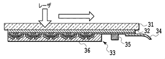
- FIG. 4A to 4G show the manufacturing process of the transparent selective bottom gate type DG-TFT formed on the polyimide resin layer.
- a polyimide resin layer 32 is formed on the carrier glass substrate 31, a transparent selection bottom gate type DG-TFT 33 is formed on the polyimide resin layer 32, and an FPC 34 and a driver LSI 35 are mounted (FIGS. 4A to 4C). Thereafter, a protective film 36 is formed so as to cover the transparent selection bottom gate type DG-TFT 33 (FIG. 4D).
- the polyimide resin layer 32 is lifted off from the carrier glass substrate 31 by irradiating laser light (line beam) from the surface of the carrier glass substrate 31 facing the polyimide resin layer 32 formation surface (FIGS. 4E to 4G). .
- the semiconductor layer of the transparent selection bottom gate type DG-TFT 33 formed on the polyimide resin layer 32 is preferably formed of i-type amorphous silicon, but the structure of the transparent selection bottom gate type DG-TFT 33 is the same as that of the first embodiment. The same.
- a film thickness of the polyimide resin layer of about several to several tens of ⁇ m is preferable because it is sufficient as an insulating substrate.
- the convexity on the detection surface of the image sensor is eliminated, thereby improving the adhesion between the detection surface and the detection object, and the distance between the detection object and the detection surface.
- it is difficult to change every time detection is performed.
Landscapes
- Engineering & Computer Science (AREA)
- Power Engineering (AREA)
- Physics & Mathematics (AREA)
- Microelectronics & Electronic Packaging (AREA)
- Condensed Matter Physics & Semiconductors (AREA)
- General Physics & Mathematics (AREA)
- Computer Hardware Design (AREA)
- Electromagnetism (AREA)
- Ceramic Engineering (AREA)
- Solid State Image Pick-Up Elements (AREA)
- Thin Film Transistor (AREA)
Abstract
検出面上に凸部を持たない透明選択ボトムゲート型DG-TFTを用いた接触型2次元イメージセンサを提供する。絶縁基板上に形成されたボトムゲート型TFTの上に、光非透過性トップゲート電極が形成されている。検出光は絶縁基板と光透過性選択ボトムゲート電極を介してボトムゲート型TFTに取り込まれる。絶縁基板(23)上に、透明選択ボトムゲート型DG-TFTフォトセンサからなるTFTフォトセンサアレイ(24)を形成し、絶縁基板(23)上のTFT形成面側にFPC(21)、ドライバLSI(22)を実装する。絶縁基板(23)上のTFT形成面と対向する裏面を検出面とするため、TFTフォトセンサアレイ(24)より大きな検出物(27)に対しても良好な密着性を実現すると共に、センサ表面を硬質な絶縁基板(23)によって検出面から隔離することで、検出物等によるスクラッチからセンサを保護する。
Description
本発明は、センサ機能と選択(読み出し)トランジスタの機能を兼ね備えたダブルゲート型薄膜トランジスタ(DG-TFT)フォトセンサを用いた、接触型2次元イメージセンサに関する。
現在、イメージセンサには、検出物とセンサとの間に距離があり、検出物の像をセンサ上に結像させるための光学系を必要とする非接触型イメージセンサと、検出物をセンサに密着させる接触型イメージセンサとがある。接触型イメージセンサとしては、TFTフォトセンサを用いたTFT駆動イメージセンサがあり、指紋センサ等に利用されている。
図5に、従来のセンサ機能と選択機能を持つフォトセンサの等価回路を示す。このフォトセンサは、ダブルゲートTFTフォトセンサ(DG-TFTフォトセンサ)と呼ばれるものであり、逆スタガー型薄膜トランジスタ(ボトムトランジスタ)とコプラナー型薄膜トランジスタ(トップトランジスタ)とを半導体層を単一層にして組み合わせたものである(特許文献1参照)。DG-TFTフォトセンサは、ボトムゲートである選択(読出し)ゲートGrに印加する電圧と、トップゲートであるセンス(蓄積)ゲートGsに印加する電圧を制御することにより、選択状態と非選択状態およびセンス状態とリセット状態とを制御することができる。このようにフォトセンサにフォトセンサ機能と選択機能とを持たせることにより、それまでフォトセンサ毎にフォトセンサとは別個に必要だった選択トランジスタを無くしてセンササイズを小さくすることができ、フォトセンサを高密度に実装することを可能にしている。
図6Aに、透明センストップゲート型DG-TFTフォトセンサを用いた2次元イメージセンサの画素回路を示し、図6Bに、フォトダイオードをセンサとして用いたTFT2次元イメージセンサの画素回路を示す。
図6AのDG-TFTフォトセンサの画素回路は、透明センストップゲート型DG-TFT61、制御線であるDataライン62-1、選択ライン62-2、蓄積ライン62-3、および保持容量63から構成される。一方、図6Bのフォトダイオードセンサの画素回路は、フォトダイオード71、トランジスタ72-1~72-4、制御線73-1~73-5、保持容量74から構成される。
このように、DG-TFTフォトセンサの画素回路は、フォトダイオードセンサに比べ単純であり高精細化に適している。
図7に、バックライトを光源とする従来の密着型TFTイメージセンサの概念図を示す。ガラス等の絶縁基板81上にTFTフォトセンサアレイ82が形成され、その上に光透過性の保護膜83が形成されて、絶縁基板81の裏面にバックライト84が設置されている。
検出面である保護膜83の表面に検出物85を密着させ、バックライト84でTFTフォトセンサアレイ82越しに検出物85に光を照射し、検出物85からの反射光をTFTフォトセンサアレイ82で検出する。DG-TFTフォトセンサのような単純な画素回路は、バックライト透過率やセンサ面積の確保が容易であり、高感度化が容易である。
図8に、従来のDG-TFTフォトセンサの構造を示す。絶縁基板90上に光非透過性選択ボトムゲート電極91、選択ゲート絶縁膜92が形成されており、選択ゲート絶縁膜92上に半導体層93、エッチングストッパ94、オーミックコンタクト層95、ソース・ドレイン電極96、センスゲート絶縁膜97が形成されている。さらにセンスゲート絶縁膜97上にソース・ドレイン電極96を覆うように光透過性センストップゲート電極98が形成され、その上に保護膜99が形成されている。
このようにDG-TFTフォトセンサは、ボトムゲート型薄膜トランジスタに光透過性のセンストップゲート電極98を組み合わせた構成を持つ。選択ボトムゲート電極91で選択(読出し)状態と非選択状態を制御し、センストップゲート電極98でセンス状態とリセット状態を制御する。検出光は、保護膜99、透明なセンストップゲート電極98、センスゲート絶縁膜97、エッチングストッパ94を透過して半導体層93に照射され、検出される。
図9Aに、従来のDG-TFTフォトセンサを用いた指紋センサモジュールの構成を示す上面図を示し、図9Bに、そのIXB-IXB’断面図を示す。
絶縁基板105上にTFTフォトセンサアレイ104、保護膜103が形成され、保護膜103上にはTFTフォトセンサアレイ104を外部回路へ接続するフレキシブルプリント配線板(FPC)101、TFTフォトセンサアレイ104を駆動するドライバLSI102が実装され、FPC101、ドライバLSI102、TFTフォトセンサアレイ104は保護膜103の開口部を介し電気的に接続されている。絶縁基板105の裏面にはバックライト106が設置されている。
DG-TFTフォトセンサは透明なセンストップゲートを有している為、TFTフォトセンサアレイ104のセンストップゲート電極が形成されている側の、保護膜103の表面が検出面となる。
しかしながら、従来のDG-TFTフォトセンサを用いたセンサモジュールにおいて、TFTフォトセンサアレイ104より広い領域をもつ検出物を取り込む際、検出面上のFPC101、ドライバLSI102等の凸部に検出物が乗り上がり、検出物と検出面との密着性が阻害されるという課題がある。
図10A、図10Bに、図9AのIXB-IXB’断面図においてTFTフォトセンサアレイより広い領域を持つ検出物の取り込み時の状況を示す。図10Aは硬質な検出物107-2の場合を示し、図10Bは軟質な検出物107-3の場合を示す。いずれの場合も、ドライバLSI102との干渉が検出物107-2、107-3と保護膜103との均質な密着を妨げ、検出像に対して全体的に、又は部分的にボケが生じる。このように、検出物と検出面との距離が検出を行う度毎に検出物の載せ方よって変化する場合、像ボケを完全に補正することは困難である。
図9A、図9B、図10A、図10Bの構造におけるセンサ表面は、0.5~数μmの保護膜103で覆われている。TFTフォトセンサアレイ104の数10~数100μmセンサピッチに比べ保護膜103の厚みは充分に小さい為、凸部を除いた像ボケは著しく小さくなる。しかし一方で、薄い保護膜103はスクラッチ等の機械的ダメージに弱く、センサや引き回し配線を破損させ易い。
本発明は、このような課題に鑑みてなされたもので、その目的とするところはセンサをスクラッチ等の機械的ダメージから保護する為に、基板のセンサ形成面に対し対抗側の表面を検出面とした、透明選択ボトムゲート型DG-TFTを用いた接触型2次元イメージセンサを提供することにある。
従来DG-TFTフォトセンサにおいて、選択ボトムゲートに透明電極、センストップゲートに不透明電極を用いた、接触型2次元イメージセンサであり、TFTフォトセンサアレイが形成された絶縁基板の、TFTフォトセンサアレイの形成面と対向する裏面を検出面とする。
本発明の接触型TFT2次元イメージセンサは、光透過性のゲート電極をもつボトムゲート型薄膜トランジスタに、光非透過性のトップゲート電極を加えたDG-TFTフォトセンサを用いる。TFTフォトセンサアレイが形成された絶縁基板のTFT形成面と対向する裏面を検出面とするため、検出面にTFT形成面側に実装されるFPCやドライバLSIによる凸部が無く、検出面と検出物との良好な密着性を実現する。
上記の課題を解決するために、本発明の一態様は、光非透過性のトップゲート電極を有するボトムゲート型薄膜トランジスタに、光透過性の絶縁膜を介して光透過性のボトムゲート電極を加えたダブルゲート型薄膜トランジスタフォトセンサからなる画素を有する接触型2次元イメージセンサであって、前記ボトムゲート電極が光透過性の絶縁基板の第1の面上に形成され、前記絶縁基板の第1の面上に前記画素を駆動する駆動回路が実装され、前記絶縁基板の第1の面と対向する前記絶縁基板の第2の面を検出面とし、検出物の前記検出面と密着した面の像を検出することを特徴とする。
本発明の別の態様は、前記トップゲート電極は、センスゲート電極であり、前記ボトムゲート電極は、選択ゲート電極であることを特徴とする。
本発明の別の態様は、前記絶縁基板は、薄板ガラスであることを特徴とする。なお、薄板ガラスは、厚いガラス上にTFTフォトセンサアレイを形成後、もしくはドライバLSIやFPC等を実装後に、化学研磨、物理研磨等によりガラスを薄型化したものでも良い。
本発明の別の態様は、前記絶縁基板は、ポリイミド樹脂層であることを特徴とする。
本発明の別の態様は、前記ダブルゲート型薄膜トランジスタフォトセンサの半導体層は、i型アモルファス・シリコンであることを特徴とする。
本発明は、密着型2次元TFTイメージセンサにおいて、イメージセンサの検出面と検出物との密着性を改善し、検出像の全体的な、又は部分的な像ボケを低減する。
また、本発明は、基板の検出面となる面と対向する面上にセンサを設け、センサ表面を基板によって検出面から隔離することにより、検出物によるスクラッチ等によるセンサの破損を防ぐ。
以下、本発明の実施の形態について、詳細に説明する。
(実施形態1)
図1に、本発明の一実施形態に係る透明選択ボトムゲート型DG-TFTの構造を示す。絶縁基板1上に形成された透明ボトムゲート型TFTの上に、センスゲート絶縁膜8を介して光非透過性センストップゲート電極9が形成されている。透明ボトムゲート型TFTは、光透過性選択ボトムゲート電極2、選択ゲート絶縁膜3、半導体層4、エッチングストッパ5、オーミックコンタクト層6、ソース・ドレイン電極7、からなり、センスゲート絶縁膜8、光非透過性センストップゲート電極9と共に保護膜10によって覆われている。検出光は絶縁基板1と光透過性選択ボトムゲート電極2を介して透明ボトムゲート型TFTに取り込まれる。光透過性選択ボトムゲート電極2の材料としては、例えば、酸化インジウムスズ(ITO)、酸化亜鉛(ZnO)、酸化スズ(SnO2)、グラフェン等を用いることができる。
図1に、本発明の一実施形態に係る透明選択ボトムゲート型DG-TFTの構造を示す。絶縁基板1上に形成された透明ボトムゲート型TFTの上に、センスゲート絶縁膜8を介して光非透過性センストップゲート電極9が形成されている。透明ボトムゲート型TFTは、光透過性選択ボトムゲート電極2、選択ゲート絶縁膜3、半導体層4、エッチングストッパ5、オーミックコンタクト層6、ソース・ドレイン電極7、からなり、センスゲート絶縁膜8、光非透過性センストップゲート電極9と共に保護膜10によって覆われている。検出光は絶縁基板1と光透過性選択ボトムゲート電極2を介して透明ボトムゲート型TFTに取り込まれる。光透過性選択ボトムゲート電極2の材料としては、例えば、酸化インジウムスズ(ITO)、酸化亜鉛(ZnO)、酸化スズ(SnO2)、グラフェン等を用いることができる。
このように、透明ボトムゲート型TFTのセンサ表面が接する面を絶縁基板1の検出面と対向する面として、センサ表面を絶縁基板1によって検出面から隔離することで、検出物等によるスクラッチからセンサを保護する。絶縁基板1の材料としては、酸化シリコンやポリイミド等の樹脂やガラス等、各種材料を使用することができる。また、絶縁基板1の厚さは一般的に数μm~1mm程度と保護膜よりも大きいため、保護膜側を検出面とするよりもセンサへの機械的ダメージを抑えることができる。
図2Aに、透明選択ボトムゲート型DG-TFTを用いた、接触型2次元イメージセンサの構造を示す上面図を示し、図2Bに、そのIIB-IIB’断面図を示す。絶縁基板23上に、透明センスボトムゲート型DG-TFTフォトセンサからなるTFTフォトセンサアレイ24を形成し、絶縁基板23上のTFT形成面側にFPC21、ドライバLSI22を実装する。TFTフォトセンサアレイ24上に保護膜25を形成し、その上にバックライト26を設置する。
絶縁基板23上のTFT形成面と対向する裏面を検出面とするため、TFTフォトセンサアレイ24より大きな検出物27に対しても良好な密着性を実現する事ができる。
図3A、図3Bに、検出物とTFT形成面との距離と反射光、散乱光の拡散範囲を示す。バックライト光は検出物27の表面で吸収、反射、散乱した後、各画素に2次元画像として取り込まれるが、検出物が検出面に密着している場合であっても絶縁基板23の厚さがt1からt2に増加すると、検出物27からの反射光、散乱光の拡散範囲が拡大し、センサ間のクロストークが増加して像ボケが強くなる。
しかしながら、像ボケは、TFTフォトセンサの開口率、TFTフォトセンサと対向する検出物との距離、TFTフォトセンサ間隔の設計値、絶縁基板23の透過率、散乱度等から補正値は見積もる事ができる。補正値は、予め読み込んだ標準パターンと、検出された値の差から見積もっても良いし、設計値と合わせて見積もってもよい。
また、よりボケの少ない画像を得る為に、エッチングや研磨等により、絶縁基板23を薄く形成しても良い。
(実施形態2)
本発明の実施形態2は、薄板ガラス基板上に形成した透明選択ボトムゲート型DG-TFTを用いた接触型2次元イメージセンサである。
本発明の実施形態2は、薄板ガラス基板上に形成した透明選択ボトムゲート型DG-TFTを用いた接触型2次元イメージセンサである。
0.4~0.5mmのキャリアガラス基板に吸着層を介して0.1mm以下の薄板ガラスを貼り付け、薄板ガラス基板上に透明選択ボトムゲート型DG-TFTを形成し、形成後キャリアガラスから薄板ガラス基板を剥離し、薄型化、フレキシブル化した密着型2次元TFTイメージセンサを製造する。薄板ガラス基板上に形成する透明センスボトムゲート型DG-TFTは、実施形態1と同様に形成可能である。
本実施形態では、エッチングや研磨等無しにTFT形成面と検出面との距離を短くでき、容易に薄型化が可能である。この薄型化により像ボケが低減すると共に、センサ表面を薄板ガラスによって検出面から隔離することで、検出物等によるスクラッチからセンサを保護し、フレキシブル化により曲面の読み込みが可能な、接触型2次元イメージセンサが実現する。
(実施形態3)
本発明の実施形態3は、薄型化、フレキシブル化の別の実施形態として、ポリイミド樹脂層上に形成した透明選択ボトムゲート型DG-TFTを用いた接触型2次元イメージセンサである。
本発明の実施形態3は、薄型化、フレキシブル化の別の実施形態として、ポリイミド樹脂層上に形成した透明選択ボトムゲート型DG-TFTを用いた接触型2次元イメージセンサである。
図4A~図4Gに、ポリイミド樹脂層上に形成された透明選択ボトムゲート型DG-TFTの製造過程を示す。キャリアガラス基板31上にポリイミド樹脂層32を形成し、ポリイミド樹脂層32上に透明選択ボトムゲート型DG-TFT33を形成し、FPC34やドライバLSI35を実装する(図4A~図4C)。その後、透明選択ボトムゲート型DG-TFT33を覆うように保護膜36を形成する(図4D)。
次に、キャリアガラス基板31のポリイミド樹脂層32形成面と対向する面からレーザ光(ラインビーム)を照射することにより、キャリアガラス基板31からポリイミド樹脂層32をリフトオフする(図4E~図4G)。
ポリイミド樹脂層32上に形成される透明選択ボトムゲート型DG-TFT33の半導体層は、i型アモルファス・シリコンで形成することが好ましいが、透明選択ボトムゲート型DG-TFT33の構造は実施形態1と同じである。ポリイミド樹脂層の膜厚としては、数~数10μm程度あれば絶縁基板として十分であり好ましい。
このように、本発明の密着型2次元TFTイメージセンサでは、イメージセンサの検出面に凸部を無くすことで、検出面と検出物との密着性を改善し、検出物と検出面との距離が検出を行う度毎に変化し難くい構成となっている。
1、23、81、105 絶縁基板
2 光透過性選択ボトムゲート電極
3 選択ゲート絶縁膜
4 半導体層
5 エッチングストッパ
6 オーミックコンタクト層
7 ソース・ドレイン電極
8 センスゲート絶縁膜
9 光非透過性センストップゲート電極
10、25、36、83、103 保護膜
21、34、101 FPC
22、35、102 ドライバLSI
24、82、104 TFTフォトセンサアレイ
26、84、106 バックライト
27、85、107 検出物
31 キャリアガラス基板
32 ポリイミド樹脂層
33 透明選択ボトムゲート型DG-TFT
61 透明センストップゲート型DG-TFT
62、73 制御線
63、74 保持容量
71 フォトダイオード
72 トランジスタ
90 絶縁基板
91 光非透過性選択ボトムゲート電極
92 選択ゲート絶縁膜
93 半導体層
94 エッチングストッパ
95 オーミックコンタクト層
96 ソース・ドレイン電極
97 センスゲート絶縁膜
98 光透過性センストップゲート電極
99 保護膜
Claims (5)
- 光透過性のボトムゲート電極を有するボトムゲート型薄膜トランジスタに、光非透過性のトップゲート電極を加えたダブルゲート型薄膜トランジスタフォトセンサからなる画素を有する接触型2次元イメージセンサであって、
前記ボトムゲート電極が光透過性の絶縁基板の第1の面上に形成され、
前記絶縁基板の第1の面上に前記画素を駆動する駆動回路が実装され、
前記絶縁基板の第1の面と対向する前記絶縁基板の第2の面を検出面とし、検出物の前記検出面と密着した面の像を検出することを特徴とする接触型2次元イメージセンサ。 - 前記トップゲート電極は、センスゲート電極であり、前記ボトムゲート電極は、選択ゲート電極であることを特徴とする請求項1に記載の接触型2次元イメージセンサ。
- 前記絶縁基板は、薄板ガラスであることを特徴とする請求項1又は2に記載の接触型2次元イメージセンサ。
- 前記絶縁基板は、ポリイミド樹脂層であることを特徴とする請求項1又は2に記載の接触型2次元イメージセンサ。
- 前記ダブルゲート型薄膜トランジスタフォトセンサの半導体層は、i型アモルファス・シリコンであることを特徴とする請求項4に記載の接触型2次元イメージセンサ。
Applications Claiming Priority (2)
| Application Number | Priority Date | Filing Date | Title |
|---|---|---|---|
| JP2015066806 | 2015-03-27 | ||
| JP2015-066806 | 2015-03-27 |
Publications (1)
| Publication Number | Publication Date |
|---|---|
| WO2016157870A1 true WO2016157870A1 (ja) | 2016-10-06 |
Family
ID=57006663
Family Applications (1)
| Application Number | Title | Priority Date | Filing Date |
|---|---|---|---|
| PCT/JP2016/001760 WO2016157870A1 (ja) | 2015-03-27 | 2016-03-25 | 接触型2次元イメージセンサ |
Country Status (1)
| Country | Link |
|---|---|
| WO (1) | WO2016157870A1 (ja) |
Cited By (1)
| Publication number | Priority date | Publication date | Assignee | Title |
|---|---|---|---|---|
| CN111943969A (zh) * | 2020-09-03 | 2020-11-17 | 山东海科新源材料科技股份有限公司 | 一种二氟草酸硼酸锂的制备方法 |
Citations (4)
| Publication number | Priority date | Publication date | Assignee | Title |
|---|---|---|---|---|
| JPS61230364A (ja) * | 1985-04-05 | 1986-10-14 | Casio Comput Co Ltd | 回路基板 |
| JPH11261047A (ja) * | 1998-03-16 | 1999-09-24 | Sharp Corp | イメージセンサ |
| JP2000208724A (ja) * | 1999-01-14 | 2000-07-28 | Casio Comput Co Ltd | 記憶素子、その駆動方法及び記憶装置、並びに撮像装置 |
| JP2003008826A (ja) * | 2001-06-26 | 2003-01-10 | Casio Comput Co Ltd | 読取装置 |
-
2016
- 2016-03-25 WO PCT/JP2016/001760 patent/WO2016157870A1/ja active Application Filing
Patent Citations (4)
| Publication number | Priority date | Publication date | Assignee | Title |
|---|---|---|---|---|
| JPS61230364A (ja) * | 1985-04-05 | 1986-10-14 | Casio Comput Co Ltd | 回路基板 |
| JPH11261047A (ja) * | 1998-03-16 | 1999-09-24 | Sharp Corp | イメージセンサ |
| JP2000208724A (ja) * | 1999-01-14 | 2000-07-28 | Casio Comput Co Ltd | 記憶素子、その駆動方法及び記憶装置、並びに撮像装置 |
| JP2003008826A (ja) * | 2001-06-26 | 2003-01-10 | Casio Comput Co Ltd | 読取装置 |
Cited By (2)
| Publication number | Priority date | Publication date | Assignee | Title |
|---|---|---|---|---|
| CN111943969A (zh) * | 2020-09-03 | 2020-11-17 | 山东海科新源材料科技股份有限公司 | 一种二氟草酸硼酸锂的制备方法 |
| CN111943969B (zh) * | 2020-09-03 | 2023-03-21 | 山东海科新源材料科技股份有限公司 | 一种二氟草酸硼酸锂的制备方法 |
Similar Documents
| Publication | Publication Date | Title |
|---|---|---|
| US10380404B2 (en) | Method and apparatus to detect three-dimensional pattern information of a touch object | |
| KR101908501B1 (ko) | 터치 스크린 일체형 유기 발광 표시 장치 및 이의 제조 방법 | |
| US20180129852A1 (en) | Display Panel And Electronic Device | |
| US8773622B2 (en) | Photodetector, liquid crystal display device, and light emitting device | |
| CN108388056B (zh) | 显示面板及其制作方法 | |
| US7999265B2 (en) | Photoelectric conversion device, electro-optic device, and electronic device | |
| TW200941087A (en) | Display device | |
| US9853164B2 (en) | Semiconductor device and display device | |
| KR20080001769A (ko) | 액정 표시 장치 및 이의 제조 방법 | |
| US9224900B2 (en) | Display device and manufacturing method thereof | |
| WO2019218715A1 (zh) | 指纹识别面板、指纹识别方法及显示装置 | |
| JP2018010829A (ja) | 表示装置 | |
| JP2020004935A (ja) | イメージセンサ | |
| WO2021261219A1 (ja) | 検出装置 | |
| WO2016157870A1 (ja) | 接触型2次元イメージセンサ | |
| US20150255616A1 (en) | Semiconductor device and display device | |
| US20150279865A1 (en) | Semiconductor device and display device | |
| WO2016092838A1 (ja) | 接触型2次元イメージセンサ | |
| CN107609542B (zh) | 光感器件、显示装置及指纹识别方法 | |
| US11997875B2 (en) | Display device and method of manufacturing the same | |
| TWI770750B (zh) | 畫素陣列基板 | |
| US12046688B2 (en) | Light sensing unit of light sensing device | |
| WO2021241051A1 (ja) | 検出装置 | |
| US20220284728A1 (en) | Detection device and method for manufacturing same | |
| KR100759273B1 (ko) | 콜리메이터가 포함된 보호필름층을 이용하여 센싱 성능과신뢰성을 높이는 접촉형 광 감지센서 장치 |
Legal Events
| Date | Code | Title | Description |
|---|---|---|---|
| 121 | Ep: the epo has been informed by wipo that ep was designated in this application |
Ref document number: 16771758 Country of ref document: EP Kind code of ref document: A1 |
|
| NENP | Non-entry into the national phase |
Ref country code: DE |
|
| NENP | Non-entry into the national phase |
Ref country code: JP |
|
| 122 | Ep: pct application non-entry in european phase |
Ref document number: 16771758 Country of ref document: EP Kind code of ref document: A1 |