WO2016157595A1 - 電子部品 - Google Patents
電子部品 Download PDFInfo
- Publication number
- WO2016157595A1 WO2016157595A1 PCT/JP2015/081368 JP2015081368W WO2016157595A1 WO 2016157595 A1 WO2016157595 A1 WO 2016157595A1 JP 2015081368 W JP2015081368 W JP 2015081368W WO 2016157595 A1 WO2016157595 A1 WO 2016157595A1
- Authority
- WO
- WIPO (PCT)
- Prior art keywords
- resin
- electronic component
- solder
- bonding material
- liquid
- Prior art date
- Legal status (The legal status is an assumption and is not a legal conclusion. Google has not performed a legal analysis and makes no representation as to the accuracy of the status listed.)
- Ceased
Links
Images



Classifications
-
- H—ELECTRICITY
- H01—ELECTRIC ELEMENTS
- H01G—CAPACITORS; CAPACITORS, RECTIFIERS, DETECTORS, SWITCHING DEVICES, LIGHT-SENSITIVE OR TEMPERATURE-SENSITIVE DEVICES OF THE ELECTROLYTIC TYPE
- H01G4/00—Fixed capacitors; Processes of their manufacture
- H01G4/002—Details
- H01G4/228—Terminals
- H01G4/232—Terminals electrically connecting two or more layers of a stacked or rolled capacitor
-
- H—ELECTRICITY
- H01—ELECTRIC ELEMENTS
- H01G—CAPACITORS; CAPACITORS, RECTIFIERS, DETECTORS, SWITCHING DEVICES, LIGHT-SENSITIVE OR TEMPERATURE-SENSITIVE DEVICES OF THE ELECTROLYTIC TYPE
- H01G4/00—Fixed capacitors; Processes of their manufacture
- H01G4/30—Stacked capacitors
-
- H—ELECTRICITY
- H05—ELECTRIC TECHNIQUES NOT OTHERWISE PROVIDED FOR
- H05K—PRINTED CIRCUITS; CASINGS OR CONSTRUCTIONAL DETAILS OF ELECTRIC APPARATUS; MANUFACTURE OF ASSEMBLAGES OF ELECTRICAL COMPONENTS
- H05K3/00—Apparatus or processes for manufacturing printed circuits
- H05K3/30—Assembling printed circuits with electric components, e.g. with resistors
- H05K3/32—Assembling printed circuits with electric components, e.g. with resistors electrically connecting electric components or wires to printed circuits
- H05K3/34—Assembling printed circuits with electric components, e.g. with resistors electrically connecting electric components or wires to printed circuits by soldering
Definitions
- the present invention relates to an electronic component, and more particularly to an electronic component that can be easily mounted.
- Solder-based bonding materials are widely used as bonding materials used in the case where electronic components including electrodes are bonded and mounted on a conductor (for example, a land electrode) on a circuit board.
- Patent Document 1 discloses a solder paste used for soldering a chip component (electronic component) having a liquidus temperature of 230 ° C. or lower and a differential thermal analysis.
- a solder paste is disclosed in which a heat absorption peak appears at the beginning of melting and then reappears when most of it melts, and then a solder alloy obtained by mixing the powder with a liquid or paste-like flux is disclosed.
- the soldering (mounting) of the chip-type electronic component can be surely performed at a low soldering temperature by using the solder paste.
- soldering is performed using the solder paste as described above (for example, the chip electronic component is mounted on the circuit board by soldering the electrode included in the chip electronic component to the land electrode on the circuit board.
- a method of mounting a chip-type electronic component on a circuit board by supplying solder paste onto a land electrode provided on the circuit board and placing the chip-type electronic component thereon and performing reflow Is widely practiced.
- the present invention solves the above problems, for example, when mounting on a mounting target, it is not necessary to prepare a bonding material such as solder separately, it is possible to simplify the mounting process, and An object is to provide an electronic component that can reduce the number of components and members to be managed in the manufacturing process and can be efficiently mounted.
- the electronic component of the present invention is characterized in that a mounting material including solder and resin is provided on the mounting surface.
- the resin constituting the bonding material includes a liquid crosslinkable resin at 15 ° C. or more and 25 ° C. or less and a solid crosslinkable resin at 15 ° C. or more and 25 ° C. or less. It is preferable.
- the resin constituting the bonding material is a liquid crosslinkable resin (hereinafter also simply referred to as “liquid resin”) at 15 ° C. or higher and 25 ° C or lower, and a solid crosslinkable resin (hereinafter referred to as “liquid resin”) at 15 ° C. or higher and 25 ° C or lower
- liquid resin a solid crosslinkable resin
- the bonding material can be appropriately molded and maintained by appropriately designing the types and blending ratios of the liquid resin and the solid resin according to the use and use conditions. It becomes possible to impart characteristics such as formability, flexibility, and adhesiveness. As a result, it is possible to provide a highly useful electronic component that has a bonding material having desirable characteristics and is excellent in handleability in a mounting process or the like.
- the crosslinkable resin is preferably a thermosetting resin.
- a thermosetting resin As the crosslinkable resin, it is possible to obtain an electronic component capable of performing highly reliable bonding only by heating, and the present invention can be more effectively realized. it can.
- thermosetting resin is preferably an epoxy resin.
- an epoxy resin as the thermosetting resin, it is possible to provide an electronic component including a bonding material capable of obtaining stable bonding reliability.
- the content ratio of the liquid crosslinkable resin and the solid crosslinkable resin is preferably in the range of 5:95 to 95: 5 by weight. Stable handling, sufficient storage stability, and high bonding reliability are realized by setting the content ratio of liquid crosslinkable resin and solid crosslinkable resin in the range of 5:95 to 95: 5 by weight.
- An electronic component including a bonding material that can be provided can be provided.
- solder is contained in a proportion of 2.5% by volume to 50% by volume. Equipped with a bonding material that can realize stable handling, sufficient storage stability, and high bonding reliability by containing solder in the bonding material at a ratio of 2.5 volume% or more and 50 volume% or less. Electronic components can be provided.
- the said solder is Sn type solder which uses Sn as one of the main components.
- Sn type solder which uses Sn as one of the main components.
- the Sn-based solder is preferably SnAgCu-based solder or SnBi-based solder.
- SnAgCu-based solder or SnBi-based solder As the Sn-based solder, it is possible to reliably provide an electronic component including a bonding material capable of realizing high bonding reliability.
- the electronic component of the present invention includes a bonding material containing solder and resin on the mounting surface, when the electronic component is mounted on a mounting target, the electronic component is prepared without separately preparing a bonding material such as solder. It is possible to easily mount the electronic component on the mounting target simply by placing the electronic component on the mounting target and heating it with a reflow furnace etc. Become.
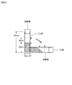
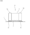
- FIG. 1 It is a front view which shows the electronic component concerning one Embodiment of this invention. It is a figure explaining the method of the liquid confirmation test done about the crosslinkable resin used in this invention. It is a figure explaining the method to mount the electronic component concerning one Embodiment of this invention on the circuit board provided with the land electrode. It is a figure which shows the other example of the electronic component of this invention, (a) is a front view, (b) is a figure which shows the state which mounts a surface mount type component. It is a figure which shows the other Example of this invention, Comprising: It is a figure which shows the state which mounts surface mount type components on a circuit board.
- FIG. 1 is a diagram showing a configuration of an electronic component according to an embodiment of the present invention.
- the electronic component body 11 constituting the electronic component 10 is a chip resistor in which a pair of external electrodes 12a and 12b are provided on both ends of the ceramic body 1, and the state shown in FIG. 1, a bonding material (a sheet-shaped bonding material in this embodiment) 3 including solder and resin is provided on the lower surface side (mounting surface) of the electronic component main body (chip resistor) 11.
- the electronic component 10 including the bonding material 3 having substantially the same size as the lower surface of the electronic component main body 11 is shown.
- the bonding material is, for example, on the lower surface side of the pair of external electrodes 12a and 12b.
- a pair of positioned bonding materials may be provided.
- the bonding material may be provided to the electronic component main body 11 in the form of being divided into three or more.
- the electronic component 10 is made of a sheet-like bonding material (sample) having a length of 0.6 mm and a width of 0.3 mm (the size of the mounting surface of the electronic component main body 11). It is formed by being cut into a corresponding dimension) and pasted on the lower surface of the electronic component main body 11.
- the bonding material 3 is made of the land electrode 2a on the circuit board 1 without separately preparing a bonding material such as solder. , 2b, the electronic component 10 can be easily mounted on the circuit board 1 simply by placing the electronic component 10 on the circuit board 1 and reflowing it. It is an electronic component.
- the bonding material constituting the electronic component 10 includes a liquid cross-linked resin (liquid resin) that is liquid at 15 ° C. or higher and 25 ° C. or lower, a solid cross-linked resin (solid resin) that is solid at 15 ° C. or higher and 25 ° C. or lower, and solder. And can be contained.
- liquid resin liquid cross-linked resin
- solid resin solid cross-linked resin
- Whether or not the cross-linked resin is “liquid at 15 ° C. or more and 25 ° C. or less” is determined by the following liquid confirmation test used for the dangerous goods determination of the Fire Service Act.
- Constant temperature water tank A stirrer, a heater, a thermometer, and an automatic temperature controller (which can be controlled at ⁇ 0.1 ° C) are prepared with a depth of 150 mm or more.
- Test tubes A flat bottom cylindrical transparent glass having an inner diameter of 30 mm and a height of 120 mm is prepared. Mark lines (hereinafter referred to as “A line” and “B line”) are attached to the test tubes at a height of 55 mm and 85 mm from the bottom of the tube.
- Thermometer (1) Prepare a freezing point (SOP-58) (scale range 20 ° C.
- test article (crosslinkable resin)
- the test article (crosslinkable resin) used for the test shall be stored at a temperature of 20 ⁇ 5 ° C. for 24 hours or more.
- thermometer is inserted so that the tip of the thermometer is 30 mm deep from the surface of the test article (crosslinked resin), and is upright with respect to the test tube.
- the two test tubes are placed in a thermostat so as to stand upright so that the line B is immersed under the water surface.
- the temperature of the test article (crosslinked resin) in the temperature measurement test tube reaches the liquid confirmation temperature ⁇ 0.1 ° C., the state is maintained for 10 minutes.
- liquid crosslinkable resin As a liquid crosslinkable resin (liquid resin) at 15 ° C. or more and 25 ° C. or less, epoxy resin, phenol resin, melamine resin, urea resin, unsaturated polyester resin, urea resin, urethane resin, polyimide resin having an appropriate molecular weight Silicone resin, acrylic resin, or the like can be used.
- Phenoxy resin epoxy resin, phenol resin, melamine resin, urea resin, unsaturated polyester, urea resin, urethane resin having an appropriate molecular weight as a solid cross-linkable resin (solid resin) at 15 ° C. or more and 25 ° C. or less,
- a polyimide resin, a silicone resin, an acrylic resin, or the like can be used.
- thermosetting resin it is usually desirable to use a thermosetting resin, but it is also possible to use a photocuring resin or a resin that crosslinks with a catalyst or the like.
- the mixing ratio of the liquid resin and the solid resin is desirably selected as the optimal mixing ratio depending on the resin to be used. However, from the viewpoint of ensuring good handleability even when the sheet is formed, the liquid resin and the solid resin
- solder constituting the bonding material it is preferable to use Sn-based solder having a relatively low melting point and capable of heat treatment at a low temperature, and among them, SnAgCu-based solder and SnBi-based solder are preferably used.
- solder materials having other compositions can be sufficiently used by applying processing conditions in accordance with their melting points.
- the amount of solder in the bonding material is preferably in the range of 2.5% by volume to 50% by volume.
- a substantially spherical shape is preferable from the viewpoint of easy material acquisition and, for example, ease of processing when processing into a sheet shape, but other shape such as a flake shape and a linear shape is preferable. It is also possible to use it.
- a substantially spherical thing as a solder, it is preferable to use a thing with an average particle diameter (D50) of 3 micrometers or more and 100 micrometers or less.
- the optimum size and blending amount can be selected according to the form of the joining object, the area and arrangement of the electrodes, and the like. However, from the viewpoint of not causing poor bonding such as open or short, it is preferable to blend a powder having an average particle diameter (D50) of 3 ⁇ m or more and 100 ⁇ m or less in a range of 2.5 volume% or more and 50 volume% or less. .
- D50 average particle diameter
- the distribution (arrangement) of the solder in the sheet-like bonding material may be uniformly distributed, and the electrodes facing each other to be bonded in consideration of the relationship with the position of the electrode in the bonding object, for example. You may make it distribute unevenly so that many may exist in between.
- an activator serves to remove solder (powder) and an oxide film on the electrode surface.
- an organic acid or amine having a function of efficiently removing solder (powder) or an oxide film on the electrode surface is used.
- organic acids are suitable from the viewpoint of activity and reliability, and adipic acid or sebacic acid is particularly preferred.
- the electronic component 10 (FIG. 1) provided with the bonding material 3 as described above is an electronic component in such a manner that the bonding material 3 faces the land electrodes 2a and 2b on the circuit board 1 as described above.
- the electronic component 10 can be easily mounted on the circuit board 1 simply by placing 10 on the circuit board 1 and heating it with a reflow furnace.
- the electrodes 12a and 12b included in the electronic component 10 and the land electrodes 2a and 2b on the circuit board 1 can be firmly bonded with solder, and the electronic component 10 and the circuit board 1 can be securely connected with resin. Therefore, highly reliable electrical connection and mechanical joining can be achieved.
- the electrodes that are to be conducted by melting the solder are securely connected via the solder, and the molten solder droplets coalesce and gather between the electrodes, so that the electrodes adjacent in the surface direction of the electrodes Short circuit between each other is also prevented.
- Example 1 Production of electronic component A
- a planar (mounting surface) dimension of a chip resistor (electronic component body) having a length of 0.6 mm and a width of 0.3 mm is formed on the mounting surface in the form of a sheet.
- An electronic component A according to an example of the present invention to which a bonding material was attached (the configuration is the same as that of the electronic component 10 according to the embodiment of the present invention illustrated in FIG. 1) was produced.
- a sheet-like bonding material prepared under the conditions described below was used as the bonding material.
- a solvent dipropylene glycol monomethyl ether acetate
- the viscosity-adjusted paste was thinly stretched using a doctor blade on a surface of a PET film that had been subjected to a release treatment on one side, and formed into a sheet shape. Then, it heat-processed on 90 degreeC and the conditions for 30 minutes in oven, and the sheet-like joining material was obtained by volatilizing a solvent. In this example, the squeegee thickness was adjusted so that the thickness of the sheet-like bonding material was about 40 ⁇ m.
- the sheet-like bonding material produced as described above is heated to 55 ° C. on a hot plate to generate an adhesive force, and the electronic component body is bonded to the sheet surface so that the mounting surface is on the lower surface side. Place on material.
- a bonding material containing solder and resin is provided on the lower surface side (mounting surface) of the electronic component body 11 in which the pair of external electrodes 12a and 12b are provided on both ends of the ceramic body.
- the electronic component A having the same structure as the electronic component 10 having the structure provided with the sheet-like bonding material 3 (in this embodiment) is obtained.
- the electronic component A according to the embodiment of the present invention formed by sticking the above-mentioned sheet-like bonding material to the electronic component main body is so arranged that the bonding material provided on the mounting surface faces the land electrode on the circuit board.
- the electronic component was placed on the circuit board and reflow heated at 245 ° C. or higher for 120 seconds or longer. As a result, it was confirmed that mounting with high electrical connection reliability and excellent mechanical joint strength can be performed.
- the phenol resin (curing agent) having the above weight average molecular weight mw 190 was used by dissolving in dipropylene glycol monomethyl ether acetate so that the proportion of the phenol resin was 65% by weight.
- This phenol resin (curing agent) is a material that also functions as a solid thermosetting resin before heating.
- the total amount of the bisphenol A type epoxy resin of the solid resin and the phenol resin (curing agent) is calculated.
- an electronic component provided with a sheet material is produced by applying a sheet-like bonding material to the electronic component body.
- An electronic component provided with a sheet material similar to the above-described electronic component A can also be produced by directly coating the substrate and heating it in an oven at 90 ° C. for 30 minutes. Even when the electronic component manufactured by this method is mounted under the same conditions as the electronic component A, the electrical connection reliability is high and the mechanical joint strength is the same as in the case of the electronic component A. It has been confirmed that excellent mounting can be achieved.
- the electronic component body constituting the electronic component (that is, the electronic component body that becomes an electronic component by providing the bonding material on the mounting surface) has special restrictions on the type, shape, structure, etc. There is no.
- the bonding material 3 can be provided on the mounting surface of the circuit board 1 provided with the land electrodes 2.
- the surface-mounted component 110 that does not include the bonding material is bonded to the circuit board 1 that includes the bonding material 3.
- FIG. 5 is a circuit diagram in which the electrodes 12 of the surface-mounted component 110 are bonded to the land electrodes 2 on the stages 20 a and 20 b of the circuit board 1 having the step 20 via the bonding material 3. A mode in which the surface-mounted component 110 is mounted on each of the stages 20a and 20b of the substrate 1 is shown.
- the mounting mode shown in FIG. 5 can be realized by mounting a surface-mounted component 110 such as a chip resistor or a ceramic capacitor that does not include a bonding material on the circuit board 1 including the bonding material 3.
- a surface-mounted component 110 such as a chip resistor or a ceramic capacitor that does not include a bonding material on the circuit board 1 including the bonding material 3.
- FIG. 6 shows a mode in which the electrode 12 of the surface-mounted component 110 is mounted on the land electrode 2 on the bottom surface 31 of the recess 30 of the circuit board 1 via the bonding material 3.
- FIG. 7 shows the case where the circuit board 1 includes a region 41 surrounded by the vertical wall 40, both main surfaces 40 a and 40 b of the vertical wall 40, and the bottom surface of the region 41 surrounded by the vertical wall 40.
- 42 shows an aspect in which the electrode 12 of the surface-mounted component 110 is mounted via the bonding material 3.
- an adhesive member such as a temporary fixing adhesive or an adhesive tape is required.
- the circuit board 1 provided with the sheet-like bonding material 3 having adhesiveness it is possible to perform mounting and bonding without particularly needing an adhesive for temporary fixing or an adhesive tape. It is particularly meaningful.
- FIG. 8 shows a mode in which the electrodes 12 of the surface-mounted component 110 are bonded to the land electrodes 2 provided on both the main surfaces 1a and 1b of the circuit board 1 with the bonding material 3 interposed therebetween.
- the bonding material used is characterized by excellent anisotropic connectivity. Therefore, the present invention is not limited by the number of terminals provided in the electronic component or the number of electrodes provided on a circuit board or the like to which the electronic component is connected (mounting target). It can be widely applied to electronic components having more terminals as well as passive components. The present invention can also be applied to various electronic module components.
- FIG. 5 shows a configuration for mounting a three-terminal type surface-mounted component 110 (110a)
- FIG. 6 shows a surface-mounted device having a large number of terminals such as an IC chip.
- a configuration for mounting the mold part 110 (110b) is shown.
Landscapes
- Engineering & Computer Science (AREA)
- Power Engineering (AREA)
- Manufacturing & Machinery (AREA)
- Microelectronics & Electronic Packaging (AREA)
- Electric Connection Of Electric Components To Printed Circuits (AREA)
Abstract
実装する場合に、別途はんだなどの接合材料を用意することが不要で、効率よく実装を行うことが可能な電子部品を提供する。 はんだと樹脂とを含む接合材料を実装面に備えた構成とする。 また、接合材料を構成する樹脂として、15℃以上、25℃以下において液状の架橋型樹脂と、15℃以上、25℃以下において固形の架橋型樹脂とを含むものを用いる。 また、架橋型樹脂として熱硬化型樹脂を用いる。 また、熱硬化型樹脂としてエポキシ樹脂を用いる。 また、液状の架橋型樹脂と固形の架橋型樹脂の含有割合を重量比で5:95~95:5の範囲とする。 はんだの含有量を、2.5体積%以上、50体積%以下の割合とする。 はんだとして、Snを主たる成分の1つとするSn系はんだを用いる。 Sn系はんだとして、SnAgCu系はんだ、またはSnBi系はんだを用いる。
Description
本発明は、電子部品に関し、詳しくは、実装を容易に行うことが可能な電子部品に関する。
電極を備える電子部品を回路基板上の導体(例えばランド電極)に接合して実装するような場合などに用いられる接合材料として、はんだ系の接合材料が広く用いられている。
そのような、はんだ系の接合材料として、特許文献1には、チップ部品(電子部品)のはんだ付けに用いられるソルダーペーストであって、液相線温度が230℃以下で、しかも示差熱分析における熱吸収のピークが溶け始めに現れ、その後大部分が溶ける際に再度ピークが現れるはんだ合金を粉末にし、該粉末と液状またはペースト状のフラックスとを混和して得たソルダーペーストが開示されている。
そして、上記ソルダーペーストを用いることにより、低いはんだ付け温度で、チップ型電子部品のはんだ付け(実装)を確実に行うことができるとされている。
そして、上記ソルダーペーストを用いることにより、低いはんだ付け温度で、チップ型電子部品のはんだ付け(実装)を確実に行うことができるとされている。
ところで、上述のようなソルダーペーストを用いてはんだ付けを行う場合(例えば、チップ型電子部品が備える電極を、回路基板上のランド電極にはんだ付けすることによりチップ型電子部品を回路基板に実装するような場合)、通常は、回路基板が備えるランド電極上にソルダーペーストを供給し、その上にチップ型電子部品を載置してリフローすることにより、チップ型電子部品を回路基板に実装する方法が広く行われている。
したがって、上述のような方法で電子部品を回路基板に実装する場合、リフローするまでに、ソルダーペーストを回路基板上に供給する工程と、チップ型電子部品をソルダーペースト上に載置する工程の2つの工程が必要になり、実装工程が複雑化するという問題点がある。
また、チップ型電子部品とソルダーペーストを別々に用意し、それぞれを保管しておくことが必要になるため、製造工程で管理すべき部品や部材など点数が多くなるという問題点がある。
本発明は、上記課題を解決するものであり、例えば、実装対象上に実装する場合に、別途はんだなどの接合材料を用意する必要がなく、実装工程を簡略化することが可能で、かつ、製造工程で管理すべき部品や部材など点数を削減することが可能で、効率よく実装を行うことができる電子部品を提供することを目的とする。
上記課題を解決するために、本発明の電子部品は、はんだと樹脂とを含む接合材料を、実装面に備えていることを特徴としている。
本発明の電子部品においては、前記接合材料を構成する前記樹脂が、15℃以上、25℃以下において液状の架橋型樹脂と、15℃以上、25℃以下において固形の架橋型樹脂とを含むものであることが好ましい。
接合材料を構成する樹脂が、15℃以上、25℃以下において液状の架橋型樹脂(以下、単に「液状樹脂」ともいう)と、15℃以上、25℃以下において固形の架橋型樹脂(以下、単に「固形樹脂」ともいう)とを含むものである場合、液状樹脂と固形樹脂の種類や配合割合などを用途や使用条件などに応じて適宜設計することにより、接合材料に、適度な成形性や保形性、柔軟性、粘着性などの特性を付与することが可能になる。
その結果、好ましい特性を有する接合材料を備えた、実装工程などにおける取り扱い性に優れた有用性の高い電子部品を提供することが可能になる。
その結果、好ましい特性を有する接合材料を備えた、実装工程などにおける取り扱い性に優れた有用性の高い電子部品を提供することが可能になる。
前記架橋型樹脂が熱硬化型樹脂であることが好ましい。
架橋型樹脂として、熱硬化型樹脂を用いることにより、加熱を行うだけで、信頼性の高い接合を行うことが可能な電子部品を得ることが可能になり、本発明をより実効あらしめることができる。
架橋型樹脂として、熱硬化型樹脂を用いることにより、加熱を行うだけで、信頼性の高い接合を行うことが可能な電子部品を得ることが可能になり、本発明をより実効あらしめることができる。
また、前記熱硬化型樹脂がエポキシ樹脂であることが好ましい。
熱硬化型樹脂としてエポキシ樹脂を用いることにより、安定した接合信頼性を得ることが可能な接合材料を備えた電子部品を提供することができる。
熱硬化型樹脂としてエポキシ樹脂を用いることにより、安定した接合信頼性を得ることが可能な接合材料を備えた電子部品を提供することができる。
前記液状の架橋型樹脂と前記固形の架橋型樹脂の含有割合が重量比で5:95~95:5の範囲にあることが好ましい。
液状の架橋型樹脂と固形の架橋型樹脂の含有割合を、重量比で5:95~95:5の範囲とすることにより、安定した取り扱い性、十分な保存安定性、高い接合信頼性を実現することが可能な接合材料を備えた電子部品を提供することができる。
液状の架橋型樹脂と固形の架橋型樹脂の含有割合を、重量比で5:95~95:5の範囲とすることにより、安定した取り扱い性、十分な保存安定性、高い接合信頼性を実現することが可能な接合材料を備えた電子部品を提供することができる。
前記はんだを2.5体積%以上、50体積%以下の割合で含むことが好ましい。
接合材料にはんだを2.5体積%以上、50体積%以下の割合で含有させることにより、安定した取り扱い性、十分な保存安定性、高い接合信頼性を実現することが可能な接合材料を備えた電子部品を提供することができる。
接合材料にはんだを2.5体積%以上、50体積%以下の割合で含有させることにより、安定した取り扱い性、十分な保存安定性、高い接合信頼性を実現することが可能な接合材料を備えた電子部品を提供することができる。
また、前記はんだがSnを主たる成分の1つとするSn系はんだであることが好ましい。
はんだを、Snを主たる成分の1つとするSn系はんだとすることにより、高い接合信頼性を実現することが可能な接合材料を備えた電子部品を提供することができる。
はんだを、Snを主たる成分の1つとするSn系はんだとすることにより、高い接合信頼性を実現することが可能な接合材料を備えた電子部品を提供することができる。
また、前記Sn系はんだがSnAgCu系はんだ、またはSnBi系はんだであることが好ましい。
Sn系はんだとしてSnAgCu系はんだ、またはSnBi系はんだを用いることにより、高い接合信頼性を実現することが可能な接合材料を備えた電子部品を確実に提供することができる。
Sn系はんだとしてSnAgCu系はんだ、またはSnBi系はんだを用いることにより、高い接合信頼性を実現することが可能な接合材料を備えた電子部品を確実に提供することができる。
本発明の電子部品は、はんだと樹脂とを含む接合材料を実装面に備えているので、電子部品を実装対象上に実装する場合に、はんだなどの接合材料を別途用意することなく、電子部品が備える接合材料が実装対象に対向するような態様で、電子部品を実装対象上に載置してリフロー炉などによって加熱するだけで、容易に電子部品を実装対象上に実装することが可能になる。
また、はんだによる電気的な接続および機械的結合と、樹脂による機械的な接合により、信頼性の高い実装を行うことが可能になる。
さらに、本発明の接合材料に液状樹脂と固形樹脂とを組み合わせて用い、液状樹脂と固形樹脂の割合を制御したり、液状樹脂および固形樹脂の種類を適切に選択したりすることにより、適度な変形性、形状保持性、柔軟性、粘着性などを付与することが可能で、さらに取り扱い性を向上させることができる。
以下に本発明を実施するための形態を示して、本発明の特徴とするところをさらに詳しく説明する。
[実施形態]
図1は、本発明の一実施形態にかかる電子部品の構成を示す図である。図1に示すように、この電子部品10を構成する電子部品本体11は、セラミック素体1の両端側に一対の外部電極12a,12bが設けられたチップ抵抗であり、図1に示した状態において、電子部品本体(チップ抵抗)11の下面側(実装面)には、はんだと樹脂とを含む接合材料(この実施形態ではシート状の接合材料)3が設けられている。
図1は、本発明の一実施形態にかかる電子部品の構成を示す図である。図1に示すように、この電子部品10を構成する電子部品本体11は、セラミック素体1の両端側に一対の外部電極12a,12bが設けられたチップ抵抗であり、図1に示した状態において、電子部品本体(チップ抵抗)11の下面側(実装面)には、はんだと樹脂とを含む接合材料(この実施形態ではシート状の接合材料)3が設けられている。
なお、この実施形態では、電子部品本体11の下面とほぼ同じ大きさの接合材料3を備えた電子部品10を示したが、接合材料は、例えば、一対の外部電極12a,12bの下面側に位置する一対の接合材料が設けられていてもよい。また、接合材料が3つ以上に分割されたかたちで電子部品本体11に対して設けられていてもよい。
この電子部品10は、例えば、図1に示すように、シート状の接合材料(試料)を、長さが0.6mm、幅が0.3mmの寸法(電子部品本体11の実装面の寸法に対応する寸法)にカットし、電子部品本体11の下面に貼り付けることにより形成される。なお、この電子部品10は、回路基板1(のランド電極2a,2b)上に実装する際に、はんだなどの接合材料を別途用意することなく、接合材料3が回路基板1上のランド電極2a,2bに対向するような態様で、電子部品10を回路基板1上に載置してリフローするだけで、容易に電子部品10の回路基板1への実装を行うことができるように構成された電子部品である。
この電子部品10を構成する接合材料は、15℃以上、25℃以下において液状の架橋型樹脂(液状樹脂)と、15℃以上、25℃以下において固形の架橋型樹脂(固形樹脂)と、はんだとを含有することができる。
架橋型樹脂について、「15℃以上、25℃以下において液状」のものであるか否かの判定は、消防法の危険物判定に用いる以下の液状確認試験により行う。
(架橋型樹脂についての液状確認試験)
[1]装置および器具
(1)恒温水槽
かくはん器、ヒーター、温度計、自動温度調節器(±0.1℃で温度制御が可能なもの)を備え、深さ150mm以上のものを用意する。
(2)試験管(2本)
内径30mm、高さ120mmの平底円筒型透明ガラス製のものを用意する。
試験管には管底から55mmおよび85mmの高さのところに標線(以下「A線」および「B線」という)を付す。
(3)温度計(1本)
「石油類試験用ガラス製温度計」(JIS B7410-1982)に規定する凝固点用(SOP-58)のもの(目盛範囲20℃~50℃)を用意する。
(4)ゴム栓(2個)
上記の(2)の試験管の口に合うものを用意する。そのうち1個には栓の中央に温度計を支える孔を設ける。
(5)ストップウォッチ
[1]装置および器具
(1)恒温水槽
かくはん器、ヒーター、温度計、自動温度調節器(±0.1℃で温度制御が可能なもの)を備え、深さ150mm以上のものを用意する。
(2)試験管(2本)
内径30mm、高さ120mmの平底円筒型透明ガラス製のものを用意する。
試験管には管底から55mmおよび85mmの高さのところに標線(以下「A線」および「B線」という)を付す。
(3)温度計(1本)
「石油類試験用ガラス製温度計」(JIS B7410-1982)に規定する凝固点用(SOP-58)のもの(目盛範囲20℃~50℃)を用意する。
(4)ゴム栓(2個)
上記の(2)の試験管の口に合うものを用意する。そのうち1個には栓の中央に温度計を支える孔を設ける。
(5)ストップウォッチ
[2]実施場所
(1)温度の調整
試験場所の温度は20±5℃に調整する。
(2)記録
温度は試験開始前および試験終了後に測定し、記録する。
(1)温度の調整
試験場所の温度は20±5℃に調整する。
(2)記録
温度は試験開始前および試験終了後に測定し、記録する。
[3]試験物品(架橋型樹脂)の調整
試験に供する試験物品(架橋型樹脂)は20±5℃の温度で24時間以上保存しているものとする。
試験に供する試験物品(架橋型樹脂)は20±5℃の温度で24時間以上保存しているものとする。
[4]確認方法
(1)恒温水槽中の水の温度を液状確認温度(液状であるか否かを確認する温度(20±5℃の範囲内の所定の温度))±0.1℃に設定する。
(2)試験物品(架橋型樹脂)を2本の試験管のA線まで注入する(図2参照)。
(3)一方の試験管を孔穴のないゴム栓で密栓する。(以下この試験管を「液状判断用試験管」という。)
(4)もう一方の試験管(以下この試験管を「温度測定用試験管」という。)は温度計をつけたゴム栓で密栓する。 ただし、温度計はその先端が試験物品(架橋型樹脂)表面より30mmの深さとなるよう挿入し、試験管に対し直立させる。
(5)2本の試験管を恒温槽中に、B線が水面下に没するよう直立させて静置させる。
(6)温度測定用試験管中の試験物品(架橋型樹脂)の温度が液状確認温度±0.1℃となってから、10分間そのままの状態を保持する。
(7)液状判断用試験管を恒温水槽から水平な台上に直立した状態のまま取り出し、直ちに台の上に水平に倒し、試験物品(架橋型樹脂)の先端がB線に到達するまでの時間を、ストップウォッチを用いて測定し、記録する。
(1)恒温水槽中の水の温度を液状確認温度(液状であるか否かを確認する温度(20±5℃の範囲内の所定の温度))±0.1℃に設定する。
(2)試験物品(架橋型樹脂)を2本の試験管のA線まで注入する(図2参照)。
(3)一方の試験管を孔穴のないゴム栓で密栓する。(以下この試験管を「液状判断用試験管」という。)
(4)もう一方の試験管(以下この試験管を「温度測定用試験管」という。)は温度計をつけたゴム栓で密栓する。 ただし、温度計はその先端が試験物品(架橋型樹脂)表面より30mmの深さとなるよう挿入し、試験管に対し直立させる。
(5)2本の試験管を恒温槽中に、B線が水面下に没するよう直立させて静置させる。
(6)温度測定用試験管中の試験物品(架橋型樹脂)の温度が液状確認温度±0.1℃となってから、10分間そのままの状態を保持する。
(7)液状判断用試験管を恒温水槽から水平な台上に直立した状態のまま取り出し、直ちに台の上に水平に倒し、試験物品(架橋型樹脂)の先端がB線に到達するまでの時間を、ストップウォッチを用いて測定し、記録する。
[5]結果の評価
上述の[4]の測定結果が90秒以内であるものを「液状」と判断する。
上述の[4]の測定結果が90秒以内であるものを「液状」と判断する。
15℃以上、25℃以下において液状の架橋型樹脂(液状樹脂)としては、適切な分子量を有するエポキシ樹脂、フェノール樹脂、メラミン樹脂、ユリア樹脂、不飽和ポリエステル樹脂、尿素樹脂、ウレタン樹脂、ポリイミド樹脂、シリコーン樹脂、アクリル樹脂などを用いることができる。
15℃以上、25℃以下において固形の架橋型樹脂(固形樹脂)としては、適切な分子量を有するフェノキシ樹脂、エポキシ樹脂、フェノール樹脂、メラミン樹脂、ユリア樹脂、不飽和ポリエステル、尿素樹脂、ウレタン樹脂、ポリイミド樹脂、シリコーン樹脂、アクリル樹脂などを用いることができる。
なお、液状樹脂および固形樹脂としては、通常、熱硬化型樹脂を用いることが望ましいが、光硬化樹脂や、触媒などにより架橋する樹脂を用いることも可能である。
液状樹脂と固形樹脂の配合割合は、使用する樹脂により最適な配合比を選択することが望ましいが、シート状にした場合にも良好な取り扱い性を確保する見地からは、液状樹脂と固形樹脂との配合割合は、液状樹脂:固形樹脂(重量比)=5:95~95:5の範囲とすることが望ましい。
液状樹脂と固形樹脂の配合割合の特に好ましい範囲は、液状樹脂:固形樹脂(重量比)=50:50~90:10の範囲である。
これは、液状樹脂の割合が50重量%未満になると、接合材料の柔軟性が低下する傾向があり、また、液状樹脂の割合が90重量%を超えると、粘性やタック性が増すため、より慎重な取り扱いが必要になることによる。
したがって、液状樹脂:固形樹脂(重量比)=50:50~90:10の範囲とすることにより、さらに取り扱い性の良好な接合材料を得ることができる。
これは、液状樹脂の割合が50重量%未満になると、接合材料の柔軟性が低下する傾向があり、また、液状樹脂の割合が90重量%を超えると、粘性やタック性が増すため、より慎重な取り扱いが必要になることによる。
したがって、液状樹脂:固形樹脂(重量比)=50:50~90:10の範囲とすることにより、さらに取り扱い性の良好な接合材料を得ることができる。
また、接合材料を構成するはんだとしては、比較的低い融点を有し、低温での熱処理が可能なSn系はんだを用いることが好ましく、その中でもSnAgCu系はんだやSnBi系はんだを用いることが好ましい。ただし、他の組成のはんだ材料でも、その融点に合わせた加工条件を適用することで十分に使用することができる。
接合材料におけるはんだの配合量は2.5体積%以上、50体積%以下の範囲とすることが望ましい。
接合材料におけるはんだの配合量は2.5体積%以上、50体積%以下の範囲とすることが望ましい。
はんだの形態としては、材料入手の容易性や、例えば、シート状に加工する際の加工の容易性の観点から略球状のものが好ましいが、リン片状、線状など別の形態のものを使用することも可能である。なお、はんだとして略球状のものを用いる場合には、平均粒径(D50)が3μm以上、100μm以下のものを用いることが好ましい。
はんだの粒径と配合量は、接合対象物の形態、電極の面積や配置などによって、最適な大きさおよび配合量を選択することができる。ただし、オープンやショートといった接合不良を起こさないという見地からは、平均粒径(D50)が3μm以上、100μm以下の粉末を2.5体積%以上、50体積%以下の範囲で配合することが好ましい。
シート状の接合材料中におけるはんだの分布(配置)については、均一に分布した状態としてもよく、また、例えば接合対象物における電極の位置との関係を考慮し、接合しようとする互いに対向する電極間に多く存在するように、不均一に分布させるようにしてもよい。
また、接合材料には、活性剤を配合することが好ましい。活性剤は、はんだ(粉末)や電極表面の酸化膜を除去する機能を果たすものである。活性剤としては、はんだ(粉末)や電極表面の酸化膜を効率よく除去する機能を有する有機酸やアミンなどが用いられる。それらのなかでも、活性度と信頼性の観点から、有機酸が適切であり、特にアジピン酸あるいはセバシン酸を用いることが好ましい。
また、上述のように接合材料3を備えた電子部品10(図1)は、上述のように、接合材料3が回路基板1上のランド電極2a,2bに対向するような態様で、電子部品10を回路基板1上に載置してリフロー炉により加熱するだけで、容易に電子部品10の回路基板1への実装を行うことができる。
すなわち、電子部品10が備える電極12a,12bと、回路基板1上のランド電極2a,2bとをはんだによって強固に接合することが可能になるとともに、電子部品10と回路基板1を、樹脂で確実に接着することができるため、電気的接続と、機械的接合の信頼性の高い実装を行うことが可能になる。
また、はんだが溶融して、導通させるべき電極どうしがはんだを介して確実に接続されるとともに、溶融したはんだの液滴が合一して電極間に集まるため、電極の面方向に隣り合う電極どうしの短絡も防止される。
[実施例]
(1)電子部品Aの作製
以下に説明する方法で、平面(実装面)寸法が、長さ0.6mm、幅が0.3mmのチップ抵抗(電子部品本体)の、実装面にシート状の接合材料が貼り付けられた本発明の実施例にかかる電子部品A(構成は図1に示した本発明の実施形態にかかる電子部品10と同じ)を作製した。
なお、この電子部品Aにおいては、接合材料として、以下に説明するような条件で調製されたシート状の接合材料を用いた。
(1)電子部品Aの作製
以下に説明する方法で、平面(実装面)寸法が、長さ0.6mm、幅が0.3mmのチップ抵抗(電子部品本体)の、実装面にシート状の接合材料が貼り付けられた本発明の実施例にかかる電子部品A(構成は図1に示した本発明の実施形態にかかる電子部品10と同じ)を作製した。
なお、この電子部品Aにおいては、接合材料として、以下に説明するような条件で調製されたシート状の接合材料を用いた。
<接合材料の組成>
(a)液状樹脂:ビスフェノールA型液状エポキシ樹脂(重量平均分子量mw380)
(b)固形樹脂:ビスフェノールA型エポキシ樹脂(重量平均分子量mw900)
(固形のビスフェノールA型エポキシ樹脂は、他の材料と混合することができるように、ジプロピレングリコールモノメチルエーテルアセテートに、ビスフェノールA型エポキシ樹脂が70重量%となるように溶かした樹脂溶液として使用)
(c)液状樹脂と固形樹脂の割合(液状樹脂/固形樹脂):90/10
(d)硬化剤:イミダゾール
(イミダゾールは、2-フェニル-4、5-ジヒドロキシメチルイミダゾールであり、液状樹脂と固形樹脂の合計量に対して6重量%になるように配合)
(e)はんだ:Sn3Ag0.5Cu
(Agが3重量%、Cuが0.5重量%、残りがSn)
(f)はんだの配合量:12体積%
(g)はんだ粒径:20μm
(h)活性剤:アジピン酸
(接合材料に含まれるはんだの量に対して一定の割合(この実施例では2重量%)となるように配合)
(a)液状樹脂:ビスフェノールA型液状エポキシ樹脂(重量平均分子量mw380)
(b)固形樹脂:ビスフェノールA型エポキシ樹脂(重量平均分子量mw900)
(固形のビスフェノールA型エポキシ樹脂は、他の材料と混合することができるように、ジプロピレングリコールモノメチルエーテルアセテートに、ビスフェノールA型エポキシ樹脂が70重量%となるように溶かした樹脂溶液として使用)
(c)液状樹脂と固形樹脂の割合(液状樹脂/固形樹脂):90/10
(d)硬化剤:イミダゾール
(イミダゾールは、2-フェニル-4、5-ジヒドロキシメチルイミダゾールであり、液状樹脂と固形樹脂の合計量に対して6重量%になるように配合)
(e)はんだ:Sn3Ag0.5Cu
(Agが3重量%、Cuが0.5重量%、残りがSn)
(f)はんだの配合量:12体積%
(g)はんだ粒径:20μm
(h)活性剤:アジピン酸
(接合材料に含まれるはんだの量に対して一定の割合(この実施例では2重量%)となるように配合)
<接合材料の成形(シート成形)>
上述の各素原料を混合して得たペーストにさらに溶剤(ジプロピレングリコールモノメチルエーテルアセテート)を加えて、塗膜形成するのに支障のない粘度に調整した。粘度調整したペーストを、片面に離形処理を施したPETフィルム上の、離形処理をした面に、ドクターブレードを用いて薄く引き延ばしてシート状に成形した。その後、オーブンで90℃、30分間の条件で加熱処理して、溶剤を揮発させることにより、シート状の接合材料を得た。この実施例では、シート状の接合材料の厚みが約40μmになるようにスキージ厚みを調整した。
上述の各素原料を混合して得たペーストにさらに溶剤(ジプロピレングリコールモノメチルエーテルアセテート)を加えて、塗膜形成するのに支障のない粘度に調整した。粘度調整したペーストを、片面に離形処理を施したPETフィルム上の、離形処理をした面に、ドクターブレードを用いて薄く引き延ばしてシート状に成形した。その後、オーブンで90℃、30分間の条件で加熱処理して、溶剤を揮発させることにより、シート状の接合材料を得た。この実施例では、シート状の接合材料の厚みが約40μmになるようにスキージ厚みを調整した。
<電子部品本体へのシート状の接合材料の付与>
上述のようにして作製した、シート状の接合材料を、ホットプレート上で55℃に加熱し、粘着力を発生させ、電子部品本体を、実装面が下面側となるように、シート状の接合材料上に載置する。
上述のようにして作製した、シート状の接合材料を、ホットプレート上で55℃に加熱し、粘着力を発生させ、電子部品本体を、実装面が下面側となるように、シート状の接合材料上に載置する。
そして、上から圧力を加えた状態で約10秒間加熱することで、シート状の接合材料と電子部品本体を十分密着させた後、シート状の接合材料を押さえながら、電子部品本体を持ち上げることにより、シート状の接合材料を電子部品本体の実装面に付与(転写)した。
これにより、図1に示すような、セラミック素体の両端側に一対の外部電極12a,12bが設けられた電子部品本体11の下面側(実装面)には、はんだと樹脂とを含む接合材料(この実施例ではシート状の接合材料)3が設けられた構造を有する電子部品10と同じ構造を有する電子部品Aが得られる。
<回路基板への電子部品Aの実装>
上述のシート状の接合材料を電子部品本体に貼り付けることにより形成した本発明の実施例にかかる電子部品Aを、その実装面に設けられた接合材料が回路基板上のランド電極に対向するような態様で、電子部品を回路基板上に載置し、245℃以上で120秒以上の条件でリフロー加熱した。
その結果、電気的な接続信頼性が高く、機械的な接合強度に優れた実装を行うことが可能になることが確認された。
上述のシート状の接合材料を電子部品本体に貼り付けることにより形成した本発明の実施例にかかる電子部品Aを、その実装面に設けられた接合材料が回路基板上のランド電極に対向するような態様で、電子部品を回路基板上に載置し、245℃以上で120秒以上の条件でリフロー加熱した。
その結果、電気的な接続信頼性が高く、機械的な接合強度に優れた実装を行うことが可能になることが確認された。
(2)変形例
(2-1)上述の電子部品Aを構成する接合材料と同じ液状樹脂と固形樹脂を用い、液状樹脂と固形樹脂の割合(液状樹脂/固形樹脂)を、80/20,70/30,60/40,50/50、30/70,10/90,5/95,95/5,0/100と変化させてシート状の接合材料を作製した。そして、このシート状の接合材料を用いて、上述の電子部品Aと同じ構成の電子部品を作製し、同じ条件で実装を行った。その結果、電気的な接続信頼性が高く、機械的な接合強度に優れた良好な実装が可能になることが確認された。
(2-1)上述の電子部品Aを構成する接合材料と同じ液状樹脂と固形樹脂を用い、液状樹脂と固形樹脂の割合(液状樹脂/固形樹脂)を、80/20,70/30,60/40,50/50、30/70,10/90,5/95,95/5,0/100と変化させてシート状の接合材料を作製した。そして、このシート状の接合材料を用いて、上述の電子部品Aと同じ構成の電子部品を作製し、同じ条件で実装を行った。その結果、電気的な接続信頼性が高く、機械的な接合強度に優れた良好な実装が可能になることが確認された。
(2-2)はんだをSn3Ag0.5Cuから、Sn58Bi(Biが58重量%、残りがSn)に代えてシート状の接合材料を作製した。そして、このシート状の接合材料を用いて、上述の電子部品Aと同じ構成の電子部品を作製し、同じ条件で実装を行った。その結果、上記電子部品Aの場合と同様に、電気的な接続信頼性と、機械的な接合強度に優れた良好な実装を行うことができることが確認された。
(2-3)はんだ(Sn3Ag0.5Cu、または、Sn58Bi)の割合を2.5体積%、6体積%、12体積%、50体積%と異ならせたシート状の接合材料、および、はんだの粒径を2.5μm、12μm、20μm、40μmと異ならせたシート状の接合材料を作製した。そして、上記接合材料を用いて電子部品Aと同じ構成の電子部品を作製し、同じ条件で実装を行った。その結果、上記電子部品Aの場合と同様に、電気的な接続信頼性が高く、機械的な接合強度に優れた良好な実装が可能になることが確認された。
(2-4)硬化剤として、フェノール樹脂(重量平均分子量mw190)を用いたシート状の接合材料を作製した。そして、このシート状の接合材料を用いて、上述の電子部品Aと同じ構成の電子部品を作製し、同じ条件で実装を行った。その結果、上記電子部品Aの場合と同様に、電気的な接続信頼性が高く、機械的な接合強度に優れた良好な実装が可能になることが確認された。
なお、上述の重量平均分子量mw190のフェノール樹脂(硬化剤)は、ジプロピレングリコールモノメチルエーテルアセテートに、フェノール樹脂の割合が65重量%となるように溶かして用いた。
このフェノール樹脂(硬化剤)は、加熱前は固形の熱硬化型樹脂としても機能する材料であり、ここでは、上記固形樹脂のビスフェノールA型エポキシ樹脂と、フェノール樹脂(硬化剤)の合計量を固形樹脂とした場合に、液状樹脂(ビスフェノールA型液状エポキシ樹脂(重量平均分子量mw380)と固形樹脂の割合が液状樹脂:固形樹脂=55:45となるようにした。
このフェノール樹脂(硬化剤)は、加熱前は固形の熱硬化型樹脂としても機能する材料であり、ここでは、上記固形樹脂のビスフェノールA型エポキシ樹脂と、フェノール樹脂(硬化剤)の合計量を固形樹脂とした場合に、液状樹脂(ビスフェノールA型液状エポキシ樹脂(重量平均分子量mw380)と固形樹脂の割合が液状樹脂:固形樹脂=55:45となるようにした。
(2-5)活性剤として、アジピン酸に代えてセバシン酸を用いたシート状の接合材料を作製した。そして、このシート状の接合材料を用いて、上述の電子部品Aと同じ構成の電子部品を作製し、同じ条件で実装を行った。その結果、上記電子部品Aの場合と同様に、電気的な接続信頼性が高く、機械的な接合強度に優れた良好な実装が可能になることが確認された。
(2-6)上記実施形態では、シート状の接合材料を電子部品本体に付与することにより、シート材料を備えた電子部品を作製するようにしたが、ペースト材料を、電子部品本体の実装面に直接塗布し、これをオーブンで90℃30分間加熱することによっても、上述の電子部品Aと同様の、シート材料を備えた電子部品を作製することができる。この方法で作製した電子部品を、上述の電子部品Aと同じ条件で実装を行った場合にも、上記電子部品Aの場合と同様に、電気的な接続信頼性が高く、機械的な接合強度に優れた良好な実装が可能になることが確認されている。
なお、本発明において、電子部品を構成する電子部品本体(すなわち、接合材料がその実装面に設けられることで電子部品となる電子部品本体)については、その種類、形状、構造などに特別の制約はない。
例えば、図4(a)に示すように、ランド電極2を備えた回路基板1の実装面に接合材料3を設けることも可能である。
この場合、図4(b)に示すように、接合材料3を備えた回路基板1に、接合材料を備えていない表面実装型部品110が接合されることになる。
図5は、段差20を有する回路基板1の各ステージ20a,20bに設けられた各ランド電極2に、表面実装型部品110の電極12が、接合材料3を介して接合されることにより、回路基板1の各ステージ20a,20bのそれぞれに、表面実装型部品110が搭載される態様を示している。
この図5に示す搭載の態様は、接合材料3を備えた回路基板1に、接合材料を備えていないチップ抵抗やセラミックコンデンサなどの表面実装型部品110を搭載することよって実現することができる。
段差20を有する回路基板1の各ステージ20a,20bに設けられた各ランド電極2に、従来のペースト状の接合材料を供給することは困難であり、生産性の低下や、実装不良などを招くおそれがあるが、実装面に接合材料3を備えた回路基板1(図5参照)を用いることにより、容易かつ確実に、信頼性の高い実装を行うことが可能になる。
図6は、回路基板1の凹部30の底面31のランド電極2に、表面実装型部品110の電極12が、接合材料3を介して搭載される態様を示している。
図6に示すように、回路基板1に接合材料3を設ける場合には、一つの接合材料3を、凹部30の底面31に備えることで、複数(2つ)の表面実装部品を一つの接合材料3で接合することが可能になり、部品点数を減らして構造を簡略化することができる。
図7は、回路基板1が、垂直壁40に囲まれた領域41を備えているような場合において、垂直壁40の両主面40a,40bと、垂直壁40に囲まれた領域41の底面42に、表面実装型部品110の電極12が、接合材料3を介して搭載される態様を示している。
図7に示すように、回路基板1の両主面40a,40b及び底面42に接合材料3を備えることにより、垂直壁40の両主面40a,40b、および、底面42に、従来のペースト状の接合材料を供給することを必要とせずに、容易かつ確実に実現することができる。
従来のペースト状の接合材料を用いて、垂直壁40の両主面40a,40bに表面実装型部品110を実装しようした場合、仮止め用の接着剤や粘着テープなどの接着部材が必要となるが、粘着性を備えたシート状の接合材料3を備えた回路基板1を用いることにより、特に仮止め用の接着剤や粘着テープなどを必要とすることなく、実装および接合を行うことが可能になり、特に有意義である。
図8は、表面実装型部品110の電極12が、接合材料3を介して、回路基板1の両主面1a,1bに設けられた各ランド電極2に接合される態様を示している。
図8に示す実装の態様の場合も、粘着性を備えた接合材料3を備えた回路基板1を用いることにより、仮止め用の接着剤や粘着テープなどを必要とすることなく、実装および接合を行うことが可能になり、特に有意義である。
本発明の電子部品においては、用いられている接合材料が、異方接続性に優れるという特徴を有している。したがって、本発明は、電子部品が備える端子の数や、電子部品が接続される対象(実装対象)である回路基板などに設けられている電極の数に制約されることがなく、2端子の受動部品はもちろん、さらに多くの端子を有する電子部品に広く適用することが可能である。また、本発明は、各種電子モジュール部品などにも適用することが可能である。
なお、図5には、3端子型の表面実装型部品110(110a)を実装する場合の構成が示されており、図6には、例えば、ICチップなどの多数の端子を備えた表面実装型部品110(110b)を実装する場合の構成が示されている。
なお、本発明は上記実施形態および実施例に限定されるものではなく、発明の範囲内において、種々の応用、変形を加えることが可能である。
1 回路基板
1a,1b 回路基板の両主面
2,2a,2b ランド電極
3 接合材料
10 電子部品
11 電子部品本体(チップ抵抗)
110 表面実装型部品
110a 3端子型の表面実装型部品
110b 多数の端子を備えた表面実装型部品
12,12a,12b 電極
20 段差
20a,20b 回路基板の各ステージ
30 回路基板の凹部
31 凹部の底面
40 回路基板の垂直壁
40a,40b 垂直壁の両主面
41 垂直壁に囲まれた領域
42 垂直壁に囲まれた領域の底面
1a,1b 回路基板の両主面
2,2a,2b ランド電極
3 接合材料
10 電子部品
11 電子部品本体(チップ抵抗)
110 表面実装型部品
110a 3端子型の表面実装型部品
110b 多数の端子を備えた表面実装型部品
12,12a,12b 電極
20 段差
20a,20b 回路基板の各ステージ
30 回路基板の凹部
31 凹部の底面
40 回路基板の垂直壁
40a,40b 垂直壁の両主面
41 垂直壁に囲まれた領域
42 垂直壁に囲まれた領域の底面
Claims (8)
- はんだと樹脂とを含む接合材料を実装面に備えていることを特徴とする電子部品。
- 前記接合材料を構成する前記樹脂が、15℃以上、25℃以下において液状の架橋型樹脂と、15℃以上、25℃以下において固形の架橋型樹脂とを含むものであることを特徴とする請求項1記載の電子部品。
- 前記架橋型樹脂が熱硬化型樹脂であることを特徴とする請求項2記載の電子部品。
- 前記熱硬化型樹脂がエポキシ樹脂であることを特徴とする請求項3記載の電子部品。
- 前記液状の架橋型樹脂と前記固形の架橋型樹脂の含有割合が重量比で5:95~95:5の範囲にあることを特徴とする請求項2~4のいずれかに記載の電子部品。
- 前記はんだを2.5体積%以上、50体積%以下の割合で含むことを特徴とする請求項1~5のいずれかに記載の電子部品。
- 前記はんだがSnを主たる成分の1つとするSn系はんだであることを特徴とする請求項1~6のいずれかに記載の電子部品。
- 前記Sn系はんだがSnAgCu系はんだ、またはSnBi系はんだであることを特徴とする請求項1~7のいずれかに記載の電子部品。
Applications Claiming Priority (4)
| Application Number | Priority Date | Filing Date | Title |
|---|---|---|---|
| JP2015-066897 | 2015-03-27 | ||
| JP2015066897 | 2015-03-27 | ||
| JP2015-106112 | 2015-05-26 | ||
| JP2015106112 | 2015-05-26 |
Publications (1)
| Publication Number | Publication Date |
|---|---|
| WO2016157595A1 true WO2016157595A1 (ja) | 2016-10-06 |
Family
ID=57006823
Family Applications (1)
| Application Number | Title | Priority Date | Filing Date |
|---|---|---|---|
| PCT/JP2015/081368 Ceased WO2016157595A1 (ja) | 2015-03-27 | 2015-11-06 | 電子部品 |
Country Status (1)
| Country | Link |
|---|---|
| WO (1) | WO2016157595A1 (ja) |
Citations (2)
| Publication number | Priority date | Publication date | Assignee | Title |
|---|---|---|---|---|
| JP2003234095A (ja) * | 2001-12-06 | 2003-08-22 | Rohm Co Ltd | 充電池用保護回路モジュール及びその製造方法 |
| JP2006110557A (ja) * | 2004-10-12 | 2006-04-27 | Matsushita Electric Ind Co Ltd | 半田ペーストおよび半田接合方法 |
-
2015
- 2015-11-06 WO PCT/JP2015/081368 patent/WO2016157595A1/ja not_active Ceased
Patent Citations (2)
| Publication number | Priority date | Publication date | Assignee | Title |
|---|---|---|---|---|
| JP2003234095A (ja) * | 2001-12-06 | 2003-08-22 | Rohm Co Ltd | 充電池用保護回路モジュール及びその製造方法 |
| JP2006110557A (ja) * | 2004-10-12 | 2006-04-27 | Matsushita Electric Ind Co Ltd | 半田ペーストおよび半田接合方法 |
Similar Documents
| Publication | Publication Date | Title |
|---|---|---|
| JP4247801B2 (ja) | ペースト状金属粒子組成物および接合方法 | |
| JP5869911B2 (ja) | 熱硬化性樹脂組成物 | |
| JP5093482B2 (ja) | 異方性導電材料、接続構造体及びその製造方法 | |
| JP5323996B2 (ja) | 加熱接合用材料、加熱接合用コーティング材料、及びコーティング物 | |
| EP0549159A2 (en) | Method and adhesive for making electrical and mechanical connections | |
| CN103907179A (zh) | 回流膜、焊料凸块形成方法、焊料接合的形成方法以及半导体装置 | |
| JP5463328B2 (ja) | パッケージ部品の接合方法およびその方法に用いる熱硬化性樹脂組成物 | |
| Liu | Reliability of surface‐mounted anisotropically conductive adhesive joints | |
| JP2018516755A (ja) | 熱可塑性ポリマーをベースとした金属導電性ホットメルトペースト | |
| KR100454861B1 (ko) | 도전성 수지, 도전성 수지를 사용한 전자 부품의 실장체,및 전자 부품의 실장체의 제조 방법 | |
| JP2009105117A (ja) | 異方性導電接着剤 | |
| JP5523454B2 (ja) | 電子部品実装構造体の製造方法 | |
| KR101733023B1 (ko) | 경화제, 그 경화제를 포함하는 열경화성 수지 조성물, 그것을 사용한 접합 방법, 및 열경화성 수지의 경화 온도의 제어 방법 | |
| JP2017126745A (ja) | 電気部品 | |
| JP5077684B2 (ja) | ピン転写用Au−Sn合金はんだペースト | |
| WO2016157595A1 (ja) | 電子部品 | |
| JP2012045617A (ja) | 導電性接合剤及びその接合方法 | |
| WO2016157594A1 (ja) | シート状の接合材料、それを備えた電子部品、接合方法、接合体 | |
| JP5370300B2 (ja) | 電子部品接合方法 | |
| JPH04190997A (ja) | 電子部品のハンダ付け用フラツクスおよび電子部品の半田付け方法 | |
| JPH0457436B2 (ja) | ||
| KR20190080250A (ko) | 솔더입자를 포함한 시트를 사용한 부품 실장 방법 | |
| JPWO2008114711A1 (ja) | 微細はんだボール配置用水溶性粘着剤 | |
| TWI885095B (zh) | 連接體、及連接體之製造方法 | |
| JPS6345892A (ja) | 面実装型電子素子の実装方法および面実装型電子素子を実装した電子装置 |
Legal Events
| Date | Code | Title | Description |
|---|---|---|---|
| 121 | Ep: the epo has been informed by wipo that ep was designated in this application |
Ref document number: 15887737 Country of ref document: EP Kind code of ref document: A1 |
|
| NENP | Non-entry into the national phase |
Ref country code: DE |
|
| NENP | Non-entry into the national phase |
Ref country code: JP |
|
| 122 | Ep: pct application non-entry in european phase |
Ref document number: 15887737 Country of ref document: EP Kind code of ref document: A1 |