WO2016157332A1 - 撮像装置 - Google Patents
撮像装置 Download PDFInfo
- Publication number
- WO2016157332A1 WO2016157332A1 PCT/JP2015/059762 JP2015059762W WO2016157332A1 WO 2016157332 A1 WO2016157332 A1 WO 2016157332A1 JP 2015059762 W JP2015059762 W JP 2015059762W WO 2016157332 A1 WO2016157332 A1 WO 2016157332A1
- Authority
- WO
- WIPO (PCT)
- Prior art keywords
- silicon substrate
- conversion film
- electrode
- container
- electron source
- Prior art date
- Legal status (The legal status is an assumption and is not a legal conclusion. Google has not performed a legal analysis and makes no representation as to the accuracy of the status listed.)
- Ceased
Links
Images

Classifications
-
- G—PHYSICS
- G01—MEASURING; TESTING
- G01T—MEASUREMENT OF NUCLEAR OR X-RADIATION
- G01T1/00—Measuring X-radiation, gamma radiation, corpuscular radiation, or cosmic radiation
- G01T1/16—Measuring radiation intensity
- G01T1/24—Measuring radiation intensity with semiconductor detectors
-
- H—ELECTRICITY
- H01—ELECTRIC ELEMENTS
- H01J—ELECTRIC DISCHARGE TUBES OR DISCHARGE LAMPS
- H01J31/00—Cathode ray tubes; Electron beam tubes
- H01J31/08—Cathode ray tubes; Electron beam tubes having a screen on or from which an image or pattern is formed, picked up, converted, or stored
- H01J31/49—Pick-up adapted for an input of electromagnetic radiation other than visible light and having an electric output, e.g. for an input of X-rays, for an input of infrared radiation
-
- H—ELECTRICITY
- H04—ELECTRIC COMMUNICATION TECHNIQUE
- H04N—PICTORIAL COMMUNICATION, e.g. TELEVISION
- H04N23/00—Cameras or camera modules comprising electronic image sensors; Control thereof
- H04N23/30—Cameras or camera modules comprising electronic image sensors; Control thereof for generating image signals from X-rays
Definitions
- the present invention relates to an imaging apparatus.
- Patent Document 1 describes an example of such an imaging apparatus.
- the imaging apparatus has a vacuum container that includes an electron source.
- the vacuum vessel has an opening connected to the space inside the vacuum vessel. This opening is closed by a glass substrate.
- a light-transmitting conductive film for example, tin oxide (SnO 2 ) or ITO (indium tin oxide)
- amorphous selenium is laminated on the translucent conductive film.
- An electrode for applying a voltage to the translucent conductive film is attached to the translucent conductive film. On the other hand, such an electrode is not attached to the outside of the substrate.
- X-rays In imaging using X-rays, it is preferable that X-rays can be detected in a wide energy range.
- An example of a problem to be solved by the present invention is that X-rays can be detected in a wide energy range in imaging using X-rays.
- a container having a space inside and having an opening connected to the space;
- a silicon substrate that closes the opening;
- An electron source provided in the space of the container and facing the silicon substrate;
- a conversion film located between the silicon substrate and the electron source, electrically connected to the silicon substrate, and converting X-rays into electric charges;
- a first electrode located on the opposite side of the conversion film through the silicon substrate and electrically connected to the silicon substrate; It is an imaging device provided with.
- FIG. 1 is a cross-sectional view illustrating a configuration of an imaging apparatus according to an embodiment.
- This imaging device includes a container 10, a silicon substrate 20, an electron source 30, a conversion film 40, and an electrode 50 (first electrode).
- the container 10 has a space inside. Furthermore, the container 10 has an opening connected to the above-described space.
- the silicon substrate 20 closes the opening of the container 10.
- the electron source 30 is provided in the above-described space of the container 10.
- the electron source 30 faces the silicon substrate 20.
- the conversion film 40 is located between the silicon substrate 20 and the electron source 30.
- the conversion film 40 is electrically connected to the silicon substrate 20.
- the conversion film 40 converts X-rays into electric charges.
- the electrode 50 is located on the opposite side of the conversion film 40 through the silicon substrate 20.
- the electrode 50 is electrically connected to the silicon substrate 20. Details will be described below.
- the container 10 includes a substrate 110 and a frame body 120.
- the substrate 110 is the bottom of the container 10, and the frame body 120 is the side surface of the container 10.
- the substrate 110 is an insulating substrate (for example, a glass substrate).
- the frame 120 has a cylindrical shape (for example, a cylindrical shape) and is mounted on the substrate 110.
- the frame body 120 is formed using an insulating member (for example, glass).
- the substrate 110 and the frame body 120 are bonded via a sealing material (for example, glass frit or indium).
- the silicon substrate 20 covers the opening of the container 10 (frame body 120) and the periphery of the opening. Thereby, the silicon substrate 20 closes the opening of the container 10.
- the silicon substrate 20 and the frame body 120 are bonded via a sealing material (for example, glass frit or indium).
- a sealing material for example, glass frit or indium.
- the electron source 30 is arranged in the space inside the container 10.
- the electron source 30 has a radiation surface 32 on the surface facing the silicon substrate 20.
- the electron source 30 can emit electrons from a plurality of regions (for example, a plurality of lattice points of m rows and n columns) arranged two-dimensionally on the emission surface 32.
- Such electrons may be emitted by scanning a surface electron source (for example, an electron source using carbon nanotubes, a Spindt-type electron source, or an electron source using HEED (High-efficiency Electron Emission Device)). it can.
- a plurality of electron guns may be arranged two-dimensionally.
- the grid electrode 14 is disposed between the silicon substrate 20 and the radiation surface 32 in the space inside the container 10. The edge of the grid electrode 14 is held on the inner surface of the frame body 120.
- the grid electrode 14 is formed of a metal (for example, Al) disposed so as to form a lattice in plan view.
- the electrons emitted from the radiation surface 32 pass through the openings of the grid electrode 14. The electrons are accelerated by the voltage applied to the grid electrode 14.
- the conversion film 40 is laminated on the silicon substrate 20.
- the conversion film 40 faces the radiation surface 32 through the grid electrode 14. Electrons radiated from the radiation surface 32 are accelerated by the grid electrode 14 and then collide with the conversion film 40.
- the conversion film 40 includes a material having an atomic weight larger than that of silicon. More specifically, the conversion film 40 is, for example, an amorphous selenium film.
- An electrode 50 is formed on the opposite side of the silicon substrate 20 to the conversion film 40.
- the conversion film 40 and the electrode 50 are opposed to each other with the silicon substrate 20 interposed therebetween. Further, a lead electrode 52 is attached to the electrode 50.
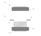
- FIG. 2 is a diagram for explaining a method of manufacturing the imaging device shown in FIG.
- an electrode 50 is formed on a silicon substrate 20 as shown in FIG.
- the electrode 50 is formed by lithography, for example. Thereby, the electrode 50 is selectively formed in a partial region of the surface of the silicon substrate 20.
- a conversion film 40 (for example, an amorphous selenium film) is deposited on the surface of the silicon substrate 20 opposite to the electrode 50.
- the conversion film 40 is formed by, for example, vacuum deposition.
- the conversion film 40 is deposited using a mask 62 having an opening. Thereby, the conversion film 40 is selectively formed in a partial region of the surface of the silicon substrate 20.
- a container 10 having an electron source 30 and a grid electrode 14 therein is prepared.
- the silicon substrate 20 is mounted on the frame body 120 (container 10) so that the conversion film 40 enters the space inside the container 10.
- the silicon substrate 20 covers the opening of the frame body 120 (container 10) and the periphery of the opening.
- the frame 120 (container 10) and the silicon substrate 20 are bonded via a sealing material (for example, glass frit or indium). Thereby, the opening of the frame 120 (container 10) is closed by the silicon substrate 20. In this way, the imaging device shown in FIG. 1 is manufactured.
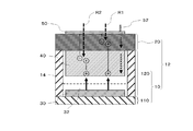
- FIG. 3 is a diagram for explaining an imaging method using the imaging apparatus shown in FIG.
- a voltage is applied to the electrode 50 via the lead electrode 52.
- an electric field is generated in the direction from the electrode 50 toward the electron source 30 in each of the silicon substrate 20 and the conversion film 40.
- X-rays are irradiated from the opposite side of the conversion film 40 through the silicon substrate 20. More specifically, in the example shown in this figure, X-ray R1 and X-ray R2 are irradiated.
- the X-ray R1 has a first energy equal to or lower than a reference energy (several keV) that can be converted into charges in the silicon substrate 20.
- the X-ray R2 has a second energy larger than the above reference energy.
- the X-ray R1 generates electron-hole pairs in the silicon substrate 20.
- the X-ray R2 passes through the silicon substrate 20 without being converted into electric charges in the silicon substrate 20 and then enters the conversion film 40.
- the conversion film 40 contains a material (for example, amorphous selenium) having an atomic weight larger than that of silicon. Therefore, the conversion film 40 can convert X-rays having energy that cannot be converted by the silicon substrate 20 (X-rays R2 in the example shown in the figure) into charges. Thereby, the X-ray R ⁇ b> 2 generates electron-hole pairs in the conversion film 40.
- a material for example, amorphous selenium
- the electrode 50 is formed using, for example, a material (for example, aluminum) that easily transmits X-rays.
- the electrode 50 may be thin enough to transmit X-rays.
- the holes generated in the silicon substrate 20 move toward the conversion film 40 side by an electric field inside the silicon substrate 20, and then enter the conversion film 40 through the interface between the silicon substrate 20 and the conversion film 40. Further, the holes move toward the electron source 30 side by the electric field inside the conversion film 40. On the other hand, the holes generated in the conversion film 40 move toward the electron source 30 side by the electric field inside the conversion film 40. Thus, in the conversion film 40, holes accumulate on the surface facing the electron source 30. And the hole pattern produced
- the holes accumulated on the surface of the conversion film 40 are scanned two-dimensionally by electrons emitted from the electron source 30.
- a current flows from the conversion film 40 to the electrode 50 through the silicon substrate 20. This current is read by the lead electrode 52.
- the hole pattern generated on the surface of the conversion film 40 can be read by reading from the electron source 30 which part of the electron source 30 has emitted electrons.
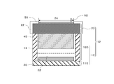
- FIG. 4 is a diagram showing a first modification of FIG.
- the imaging device may include an insulating material 22.
- the insulating material 22 is, for example, an insulating resin.
- the insulating material 22 is located around the electrode 50 and covers the silicon substrate 20. Furthermore, in the example shown in this drawing, the insulating material 22 is in contact with the side surface of the electrode 50. Thereby, the surface of the silicon substrate 20 exposed to the outside is covered with the insulating material 22 and the electrode 50. Thereby, the silicon substrate 20 can be electrically isolated from the external region. However, the insulating material 22 may be separated from the side surface of the electrode 50. Also in this case, when the surface area of the silicon substrate 20 exposed between the insulating material 22 and the electrode 50 is small to some extent, the silicon substrate 20 can be electrically separated from the external region.
- the insulating material 22 has an opening 24.
- the opening 24 includes the electrode 50 on the inner side in a plan view.
- the inner surface of the opening 24 is in contact with the side surface of the electrode 50.
- Such an opening 24 is formed, for example, by providing the insulating material 22 around the electrode 50 after providing the electrode 50 on the silicon substrate 20.
- the opening 24 may be formed by selectively removing the insulating film (insulating material 22) formed on the silicon substrate 20.
- the electrode 50 is provided on the silicon substrate 20 after the opening 24 is formed, for example.
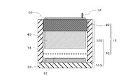
- FIG. 5 is a diagram showing a second modification of FIG.
- the side surface of the silicon substrate 20 may be fitted into the inner side surface of the frame body 120.
- a sealing material for example, glass frit or indium
- the silicon substrate 20 can block the opening of the container 10.
- the insulating material 22 (FIG. 4) may be provided on the upper surface of the silicon substrate 20 (for example, a portion not covered with the electrode 50).
- the conversion film 40 can convert X-rays having energy that cannot be converted by the silicon substrate 20 into electric charges. Thereby, even if the silicon substrate 20 is irradiated with X-rays having energy that cannot be converted by the silicon substrate 20, the X-rays can be converted in the conversion film 40. Thereby, X-rays can be detected in a wide energy range.
- the silicon substrate 20 is a part of the outer wall of the vacuum vessel 12. For this reason, electrodes (for example, the electrode 50 and the lead electrode 52) for applying a voltage to the silicon substrate 20 can be provided outside the vacuum container 12.
Landscapes
- Physics & Mathematics (AREA)
- Electromagnetism (AREA)
- Health & Medical Sciences (AREA)
- Life Sciences & Earth Sciences (AREA)
- General Physics & Mathematics (AREA)
- High Energy & Nuclear Physics (AREA)
- Molecular Biology (AREA)
- Spectroscopy & Molecular Physics (AREA)
- Measurement Of Radiation (AREA)
- Solid State Image Pick-Up Elements (AREA)
Abstract
X線を用いた撮像において、広いエネルギー範囲でX線を検出可能とする。 撮像装置は、容器(10)を備える。容器(10)は、内部に空間を有している。さらに、容器(10)は、上記した空間に繋がる開口を有している。シリコン基板(20)は、容器(10)の開口を塞いでいる。電子源(30)は、容器(10)の上記した空間内に設けられている。電子源(30)は、シリコン基板(20)に対向している。変換膜(40)は、シリコン基板(20)と電子源(30)の間に位置している。変換膜(40)は、シリコン基板(20)に電気的に接続している。変換膜(40)は、X線を電荷に変換する。電極(50)は、シリコン基板(20)を介して変換膜(40)の反対側に位置している。電極(50)は、シリコン基板(20)に電気的に接続している。
Description
本発明は、撮像装置に関する。
近年、電子源アレイと光電変換膜を用いた撮像装置が開発されている。特許文献1には、このような撮像装置の一例が記載されている。この例において、撮像装置は、電子源を内部に含む真空容器を有している。真空容器は、真空容器の内部の空間に繋がる開口を有している。この開口は、ガラス基板によって塞がれている。真空容器の内部の空間において、基板には、透光性導電膜(例えば、酸化スズ(SnO2)又はITO(酸化インジウムスズ))が積層されている。さらに、透光性導電膜には、アモルファスセレンが積層されている。透光性導電膜には、透光性導電膜に電圧を印加するための電極が取り付けられている。これに対して、基板の外部には、このような電極が取り付けられていない。
X線を用いた撮像では、広いエネルギー範囲でX線が検出可能であることが好ましい。
本発明が解決しようとする課題としては、X線を用いた撮像において、広いエネルギー範囲でX線を検出可能にすることが一例として挙げられる。
請求項1に記載の発明は、
内部に空間を有し、前記空間に繋がる開口を有する容器と、
前記開口を塞ぐシリコン基板と、
前記容器の前記空間内に設けられ、前記シリコン基板に対向する電子源と、
前記シリコン基板と前記電子源の間に位置し、前記シリコン基板に電気的に接続し、X線を電荷に変換する変換膜と、
前記シリコン基板を介して前記変換膜の反対側に位置し、前記シリコン基板に電気的に接続する第1電極と、
を備える撮像装置である。
内部に空間を有し、前記空間に繋がる開口を有する容器と、
前記開口を塞ぐシリコン基板と、
前記容器の前記空間内に設けられ、前記シリコン基板に対向する電子源と、
前記シリコン基板と前記電子源の間に位置し、前記シリコン基板に電気的に接続し、X線を電荷に変換する変換膜と、
前記シリコン基板を介して前記変換膜の反対側に位置し、前記シリコン基板に電気的に接続する第1電極と、
を備える撮像装置である。
上述した目的、およびその他の目的、特徴および利点は、以下に述べる好適な実施の形態、およびそれに付随する以下の図面によってさらに明らかになる。
以下、本発明の実施の形態について、図面を用いて説明する。尚、すべての図面において、同様な構成要素には同様の符号を付し、適宜説明を省略する。
図1は、実施形態に係る撮像装置の構成を示す断面図である。この撮像装置は、容器10、シリコン基板20、電子源30、変換膜40、及び電極50(第1電極)を備える。容器10は、内部に空間を有している。さらに、容器10は、上記した空間に繋がる開口を有している。シリコン基板20は、容器10の開口を塞いでいる。電子源30は、容器10の上記した空間内に設けられている。電子源30は、シリコン基板20に対向している。変換膜40は、シリコン基板20と電子源30の間に位置している。変換膜40は、シリコン基板20に電気的に接続している。変換膜40は、X線を電荷に変換する。電極50は、シリコン基板20を介して変換膜40の反対側に位置している。電極50は、シリコン基板20に電気的に接続している。以下、詳細に説明する。
本図に示す例において、容器10は、基板110及び枠体120を備えている。基板110は容器10の底となっており、枠体120は容器10の側面となっている。基板110は、絶縁性基板(例えば、ガラス基板)である。枠体120は、筒状(例えば、円筒状)の形状を有しており、基板110に搭載されている。なお、枠体120は、絶縁性部材(例えば、ガラス)を用いて形成されている。基板110と枠体120は、封止材(例えば、ガラスフリット又はインジウム)を介して接着している。
本図に示す例において、シリコン基板20は、容器10(枠体120)の上記した開口及びその開口の周囲を覆っている。これにより、シリコン基板20は、容器10の開口を塞いでいる。シリコン基板20と枠体120は、封止材(例えば、ガラスフリット又はインジウム)を介して接着している。このようにして、容器10及びシリコン基板20は、真空容器12を構成している。そして、真空容器12の内側の空間は、外部の空間から遮断される。
容器10の内部の空間には、電子源30が配置されている。電子源30は、シリコン基板20と対向する面に放射面32を有している。電子源30は、放射面32において2次元的に配列された複数の領域(例えば、m行n列の複数の格子点)それぞれから電子を放射することができる。このような電子は、面電子源(例えば、カーボンナノチューブを用いた電子源、Spindt型電子源、又はHEED(High-efficiency Electron Emission Device)を用いた電子源)を走査することにより放射することができる。他の例として、複数の電子銃を2次元的に配列してもよい。
容器10の内部の空間には、シリコン基板20と放射面32の間にグリッド電極14が配置されている。グリッド電極14は、縁が枠体120の内側面に保持されている。グリッド電極14は、平面視において格子を構成するように配置された金属(例えば、Al)により形成されている。放射面32から放射された電子は、グリッド電極14の開口を通過する。そしてこの電子は、グリッド電極14に印加された電圧によって加速する。
容器10の内部の空間では、シリコン基板20に変換膜40が積層されている。変換膜40は、グリッド電極14を介して放射面32と対向している。放射面32から放射された電子は、グリッド電極14によって加速され、その後、変換膜40に衝突する。変換膜40は、シリコンより原子量の大きい材料を含んでいる。より具体的には、変換膜40は、例えば、アモルファスセレン膜である。
シリコン基板20のうち変換膜40の反対側には、電極50が形成されている。変換膜40及び電極50は、シリコン基板20を介して互いに対向している。さらに、電極50には、リード電極52が取り付けられている。
図2は、図1に示した撮像装置の製造方法を説明するための図である。まず、本図(a)に示すように、シリコン基板20上に電極50を形成する。電極50は、例えば、リソグラフィにより形成される。これにより、電極50は、シリコン基板20の表面の一部の領域に選択的に形成される。
次いで、本図(b)に示すように、シリコン基板20のうち電極50とは反対側の面に変換膜40(例えば、アモルファスセレン膜)を堆積する。変換膜40は、例えば、真空蒸着により形成される。そして本図に示す例では、開口を有するマスク62を用いて変換膜40を堆積している。これにより、シリコン基板20の表面の一部の領域に変換膜40が選択的に形成される。
次いで、図1に示したように、電子源30及びグリッド電極14を内部に有する容器10を準備する。次いで、容器10の内部の空間に変換膜40が入り込む向きにシリコン基板20を枠体120(容器10)に搭載する。この場合、シリコン基板20が枠体120(容器10)の開口及びその開口の周囲を覆うようにする。そして枠体120(容器10)とシリコン基板20を、封止材(例えば、ガラスフリット又はインジウム)を介して接着する。これにより、枠体120(容器10)の開口がシリコン基板20によって塞がれる。このようにして、図1に示した撮像装置が製造される。
図3は、図1に示した撮像装置を用いた撮像方法を説明するための図である。本図に示す例では、リード電極52を介して電極50に電圧を印加している。これにより、シリコン基板20の内部及び変換膜40の内部それぞれにおいて電極50から電子源30に向かう方向に電界を発生させている。
本図に示す例において、X線は、シリコン基板20を介して変換膜40の反対側から照射される。より詳細には、本図に示す例では、X線R1及びX線R2が照射されている。X線R1は、シリコン基板20において電荷に変換可能な基準エネルギー(数keV)以下の第1エネルギーを有する。X線R2は、上記した基準エネルギーよりも大きい第2エネルギーを有する。本図に示すように、X線R1は、シリコン基板20において電子正孔対を生成する。一方、X線R2は、シリコン基板20において電荷に変換されることなくシリコン基板20を透過し、その後、変換膜40に入り込む。変換膜40は、シリコンより原子量の大きい材料(例えば、アモルファスセレン)を含んでいる。このため、変換膜40は、シリコン基板20によって変換することができないエネルギーを有するX線(本図に示す例では、X線R2)であっても電荷に変換することができる。これにより、X線R2は、変換膜40において電子正孔対を生成する。
なお、X線がシリコン基板20に入り込むためには、X線が電極50を透過する必要がある。このため、電極50は、例えば、X線が透過しやすい材料(例えば、アルミニウム)を用いて形成されている。その他の例として、電極50は、X線が透過することができる程膜厚を薄いものとしてもよい。
シリコン基板20において発生した正孔は、シリコン基板20の内部の電界によって、変換膜40側に向かって移動し、その後、シリコン基板20と変換膜40の界面を通過して変換膜40に入り込む。さらに、この正孔は、変換膜40の内部の電界によって、電子源30側に向かって移動する。一方、変換膜40において発生した正孔は、変換膜40の内部の電界によって、電子源30側に向かって移動する。このようにして、変換膜40では、電子源30と対向する表面に正孔が蓄積することになる。そしてこの場合に生成される正孔パターンは、撮像装置に入射したX線の像に対応したものとなる。
変換膜40の表面に蓄積した正孔は、電子源30から放射される電子によって2次元的に走査される。この場合、電子源30からの電子が正孔と結合すると、変換膜40からシリコン基板20を介して電極50に電流が流れる。そしてこの電流は、リード電極52によって読み出される。この場合、電子源30のいずれの部分から電子が放射されたかを電子源30から読み出すことにより、変換膜40の表面に生成された正孔パターンを読み出すことができる。
図4は、図1の第1の変形例を示す図である。本図に示すように、撮像装置は、絶縁材22を備えていてもよい。絶縁材22は、例えば、絶縁性樹脂である。絶縁材22は、電極50の周囲に位置し、シリコン基板20を覆っている。さらに、本図に示す例では、絶縁材22は、電極50の側面に接している。これにより、シリコン基板20は、外部に露出されている表面が絶縁材22及び電極50によって覆われる。これにより、シリコン基板20を外部の領域から電気的に分離することができる。ただし、絶縁材22は、電極50の側面から離れていてもよい。この場合においても、シリコン基板20のうち絶縁材22と電極50の間で露出する表面の面積がある程度小さいときは、シリコン基板20を外部の領域から電気的に分離することができる。
本図に示す例において、絶縁材22は、開口24を有している。開口24は、平面視において、電極50を内側に含んでいる。開口24の内側面は、電極50の側面に接している。このような開口24は、例えば、シリコン基板20に電極50を設けた後、電極50の周囲に絶縁材22を設けることで形成される。ただし、開口24は、シリコン基板20に形成された絶縁膜(絶縁材22)を選択的に除去することにより形成してもよい。この場合、電極50は、例えば、開口24が形成された後にシリコン基板20に設けられる。
図5は、図1の第2の変形例を示す図である。本図に示すように、シリコン基板20は、側面が枠体120の内側面にはめ込まれていてもよい。なお、シリコン基板20の側面と枠体120の内側面の間には、封止材(例えば、ガラスフリット又はインジウム)を設けてもよい。本図に示す例においても、シリコン基板20は、容器10の開口を塞ぐことができる。なお、本図に示す例においても、シリコン基板20の上面(例えば、電極50によって覆われていない部分)に絶縁材22(図4)を設けてもよい。
以上、本実施形態によれば、変換膜40は、シリコン基板20によって変換することができないエネルギーを有するX線を電荷に変換することができる。これにより、シリコン基板20によって変換することができないエネルギーを有するX線がシリコン基板20に照射されたとしても、このX線を変換膜40において変換することができる。これにより、広いエネルギー範囲でX線を検出することができる。
さらに、本実施形態によれば、シリコン基板20は、真空容器12の外壁の一部となっている。このため、シリコン基板20に電圧を印加するための電極(例えば、電極50及びリード電極52)を真空容器12の外側に設けることができる。
以上、図面を参照して実施形態及び実施例について述べたが、これらは本発明の例示であり、上記以外の様々な構成を採用することもできる。
Claims (7)
- 内部に空間を有し、前記空間に繋がる開口を有する容器と、
前記開口を塞ぐシリコン基板と、
前記容器の前記空間内に設けられ、前記シリコン基板に対向する電子源と、
前記シリコン基板と前記電子源の間に位置し、前記シリコン基板に電気的に接続し、X線を電荷に変換する変換膜と、
前記シリコン基板を介して前記変換膜の反対側に位置し、前記シリコン基板に電気的に接続する第1電極と、
を備える撮像装置。 - 請求項1に記載の撮像装置において、
前記変換膜は、シリコンより原子量の大きい材料を含む撮像装置。 - 請求項2に記載の撮像装置において、
前記材料は、セレンである撮像装置。 - 請求項1~3のいずれか一項に記載の撮像装置において、
前記シリコン基板は、前記開口及びその周囲を覆っている撮像装置。 - 請求項1~3のいずれか一項に記載の撮像装置において、
前記シリコン基板は、前記容器の内側面にはめ込まれている撮像装置。 - 請求項1~5のいずれか一項に記載の撮像装置において、
前記第1電極の周囲に位置し、前記シリコン基板を覆う絶縁材を備える撮像装置。 - 請求項6に記載の撮像装置において、
前記絶縁材は、前記第1電極の少なくとも一部に接する撮像装置。
Priority Applications (1)
| Application Number | Priority Date | Filing Date | Title |
|---|---|---|---|
| PCT/JP2015/059762 WO2016157332A1 (ja) | 2015-03-27 | 2015-03-27 | 撮像装置 |
Applications Claiming Priority (1)
| Application Number | Priority Date | Filing Date | Title |
|---|---|---|---|
| PCT/JP2015/059762 WO2016157332A1 (ja) | 2015-03-27 | 2015-03-27 | 撮像装置 |
Publications (1)
| Publication Number | Publication Date |
|---|---|
| WO2016157332A1 true WO2016157332A1 (ja) | 2016-10-06 |
Family
ID=57005870
Family Applications (1)
| Application Number | Title | Priority Date | Filing Date |
|---|---|---|---|
| PCT/JP2015/059762 Ceased WO2016157332A1 (ja) | 2015-03-27 | 2015-03-27 | 撮像装置 |
Country Status (1)
| Country | Link |
|---|---|
| WO (1) | WO2016157332A1 (ja) |
Citations (2)
| Publication number | Priority date | Publication date | Assignee | Title |
|---|---|---|---|---|
| JP2009186475A (ja) * | 2008-02-05 | 2009-08-20 | Panalytical Bv | 画像化検出器 |
| JP2010028267A (ja) * | 2008-07-16 | 2010-02-04 | Pioneer Electronic Corp | 撮像装置 |
-
2015
- 2015-03-27 WO PCT/JP2015/059762 patent/WO2016157332A1/ja not_active Ceased
Patent Citations (2)
| Publication number | Priority date | Publication date | Assignee | Title |
|---|---|---|---|---|
| JP2009186475A (ja) * | 2008-02-05 | 2009-08-20 | Panalytical Bv | 画像化検出器 |
| JP2010028267A (ja) * | 2008-07-16 | 2010-02-04 | Pioneer Electronic Corp | 撮像装置 |
Similar Documents
| Publication | Publication Date | Title |
|---|---|---|
| US10580630B2 (en) | Photomultiplier tube and method of making it | |
| US6720996B1 (en) | Imaging apparatus | |
| CN1415076A (zh) | 射线照相的方法与装置和辐射检测器 | |
| CN117642836A (zh) | 带电粒子检测器组件 | |
| US20160161426A1 (en) | Pillar Based Amorphous and Polycrystalline Photoconductors for X-ray Image Sensors | |
| KR20150024720A (ko) | 평판형 엑스선 발생기 및 이를 구비하는 엑스선 영상 시스템 | |
| KR20180065861A (ko) | 전계 방출 장치 | |
| JPH1050241A (ja) | 電界放出デバイス収納真空容器 | |
| EP3350825B1 (en) | A phototube and method of making it | |
| JP2010212087A (ja) | 撮像素子及び耐放射線カメラ | |
| WO2017017811A1 (ja) | 撮像装置 | |
| JP2005268722A (ja) | 放射線検出器およびその製造方法 | |
| US10804085B2 (en) | Photomultiplier and methods of making it | |
| JP2006524077A (ja) | 大面積検出器およびディスプレイ | |
| EP0760525B1 (en) | Electron tube | |
| WO2016139724A1 (ja) | 撮像装置 | |
| RU2324256C1 (ru) | Электронно-чувствительная матрица с переносом заряда для электронно-оптических преобразователей (варианты) | |
| JP5503387B2 (ja) | 光導電素子及び撮像デバイス | |
| RU2622397C2 (ru) | Высоковольтный гибридный фоточувствительный прибор для регистрации излучения малой интенсивности | |
| JP2009123423A (ja) | 撮像デバイス | |
| JP5000254B2 (ja) | 撮像装置 | |
| CN121816520A (zh) | 一种用于探测X射线、γ射线和中子的方法及装置 | |
| JPS61153934A (ja) | 焦点位置可変形x線管 | |
| JP2014082008A (ja) | 撮像デバイス | |
| KR101245526B1 (ko) | 집광렌즈를 이용한 pdp패널 기반의 디지털 엑스-선 영상검출기 |
Legal Events
| Date | Code | Title | Description |
|---|---|---|---|
| 121 | Ep: the epo has been informed by wipo that ep was designated in this application |
Ref document number: 15887485 Country of ref document: EP Kind code of ref document: A1 |
|
| NENP | Non-entry into the national phase |
Ref country code: DE |
|
| NENP | Non-entry into the national phase |
Ref country code: JP |
|
| 122 | Ep: pct application non-entry in european phase |
Ref document number: 15887485 Country of ref document: EP Kind code of ref document: A1 |