WO2016143608A1 - Motor control apparatus, heat pump system, and air conditioner - Google Patents
Motor control apparatus, heat pump system, and air conditioner Download PDFInfo
- Publication number
- WO2016143608A1 WO2016143608A1 PCT/JP2016/056249 JP2016056249W WO2016143608A1 WO 2016143608 A1 WO2016143608 A1 WO 2016143608A1 JP 2016056249 W JP2016056249 W JP 2016056249W WO 2016143608 A1 WO2016143608 A1 WO 2016143608A1
- Authority
- WO
- WIPO (PCT)
- Prior art keywords
- phase
- current
- duty
- current detection
- timing
- Prior art date
Links
Images


Classifications
-
- H—ELECTRICITY
- H02—GENERATION; CONVERSION OR DISTRIBUTION OF ELECTRIC POWER
- H02P—CONTROL OR REGULATION OF ELECTRIC MOTORS, ELECTRIC GENERATORS OR DYNAMO-ELECTRIC CONVERTERS; CONTROLLING TRANSFORMERS, REACTORS OR CHOKE COILS
- H02P27/00—Arrangements or methods for the control of AC motors characterised by the kind of supply voltage
- H02P27/04—Arrangements or methods for the control of AC motors characterised by the kind of supply voltage using variable-frequency supply voltage, e.g. inverter or converter supply voltage
- H02P27/06—Arrangements or methods for the control of AC motors characterised by the kind of supply voltage using variable-frequency supply voltage, e.g. inverter or converter supply voltage using dc to ac converters or inverters
- H02P27/08—Arrangements or methods for the control of AC motors characterised by the kind of supply voltage using variable-frequency supply voltage, e.g. inverter or converter supply voltage using dc to ac converters or inverters with pulse width modulation
- H02P27/085—Arrangements or methods for the control of AC motors characterised by the kind of supply voltage using variable-frequency supply voltage, e.g. inverter or converter supply voltage using dc to ac converters or inverters with pulse width modulation wherein the PWM mode is adapted on the running conditions of the motor, e.g. the switching frequency
-
- F—MECHANICAL ENGINEERING; LIGHTING; HEATING; WEAPONS; BLASTING
- F04—POSITIVE - DISPLACEMENT MACHINES FOR LIQUIDS; PUMPS FOR LIQUIDS OR ELASTIC FLUIDS
- F04B—POSITIVE-DISPLACEMENT MACHINES FOR LIQUIDS; PUMPS
- F04B49/00—Control, e.g. of pump delivery, or pump pressure of, or safety measures for, machines, pumps, or pumping installations, not otherwise provided for, or of interest apart from, groups F04B1/00 - F04B47/00
- F04B49/06—Control using electricity
-
- F—MECHANICAL ENGINEERING; LIGHTING; HEATING; WEAPONS; BLASTING
- F25—REFRIGERATION OR COOLING; COMBINED HEATING AND REFRIGERATION SYSTEMS; HEAT PUMP SYSTEMS; MANUFACTURE OR STORAGE OF ICE; LIQUEFACTION SOLIDIFICATION OF GASES
- F25B—REFRIGERATION MACHINES, PLANTS OR SYSTEMS; COMBINED HEATING AND REFRIGERATION SYSTEMS; HEAT PUMP SYSTEMS
- F25B49/00—Arrangement or mounting of control or safety devices
- F25B49/02—Arrangement or mounting of control or safety devices for compression type machines, plants or systems
- F25B49/025—Motor control arrangements
-
- H—ELECTRICITY
- H02—GENERATION; CONVERSION OR DISTRIBUTION OF ELECTRIC POWER
- H02P—CONTROL OR REGULATION OF ELECTRIC MOTORS, ELECTRIC GENERATORS OR DYNAMO-ELECTRIC CONVERTERS; CONTROLLING TRANSFORMERS, REACTORS OR CHOKE COILS
- H02P27/00—Arrangements or methods for the control of AC motors characterised by the kind of supply voltage
- H02P27/04—Arrangements or methods for the control of AC motors characterised by the kind of supply voltage using variable-frequency supply voltage, e.g. inverter or converter supply voltage
- H02P27/06—Arrangements or methods for the control of AC motors characterised by the kind of supply voltage using variable-frequency supply voltage, e.g. inverter or converter supply voltage using dc to ac converters or inverters
- H02P27/08—Arrangements or methods for the control of AC motors characterised by the kind of supply voltage using variable-frequency supply voltage, e.g. inverter or converter supply voltage using dc to ac converters or inverters with pulse width modulation
-
- H—ELECTRICITY
- H02—GENERATION; CONVERSION OR DISTRIBUTION OF ELECTRIC POWER
- H02P—CONTROL OR REGULATION OF ELECTRIC MOTORS, ELECTRIC GENERATORS OR DYNAMO-ELECTRIC CONVERTERS; CONTROLLING TRANSFORMERS, REACTORS OR CHOKE COILS
- H02P6/00—Arrangements for controlling synchronous motors or other dynamo-electric motors using electronic commutation dependent on the rotor position; Electronic commutators therefor
- H02P6/14—Electronic commutators
- H02P6/16—Circuit arrangements for detecting position
- H02P6/18—Circuit arrangements for detecting position without separate position detecting elements
-
- F—MECHANICAL ENGINEERING; LIGHTING; HEATING; WEAPONS; BLASTING
- F25—REFRIGERATION OR COOLING; COMBINED HEATING AND REFRIGERATION SYSTEMS; HEAT PUMP SYSTEMS; MANUFACTURE OR STORAGE OF ICE; LIQUEFACTION SOLIDIFICATION OF GASES
- F25B—REFRIGERATION MACHINES, PLANTS OR SYSTEMS; COMBINED HEATING AND REFRIGERATION SYSTEMS; HEAT PUMP SYSTEMS
- F25B2600/00—Control issues
- F25B2600/02—Compressor control
- F25B2600/021—Inverters therefor
Definitions
- Embodiments of the present invention provide a control device that controls a motor via an inverter circuit by PWM-controlling a plurality of switching elements connected in a three-phase bridge, a heat pump system including the control device, and an air conditioner About.
- the present invention provides a motor control device that can employ a current detection method using one current detection element while avoiding an increase in switching loss, and a heat pump system and an air conditioner including the control device.
- the current detection unit calculates the phase current of the motor based on the signal generated by the current detection element connected to the DC side of the inverter circuit corresponding to the current value and the PWM signal pattern. Then, the rotor position determination unit determines the rotor position based on the phase current, and the PWM signal generation unit generates a two-phase or three-phase PWM signal pattern so as to follow the rotor position.
- the current detection rate calculation unit obtains a current detection rate according to the two-phase or three-phase PWM signal pattern, and the timing adjustment unit fixes the two-phase current within the carrier wave period of the PWM signal. Or at a variable timing according to the magnitude of the output voltage to the inverter circuit.
- the PWM signal generation unit increases / decreases the duty in both directions of the delay side and the advance side with respect to the arbitrary phase of the carrier wave period for the first phase of the three-phase PWM signal patterns, and for the second phase. Increases or decreases the duty in one direction of the delay side and the advance side with respect to an arbitrary phase of the carrier wave cycle, and for the third phase, increases or decreases the duty in the opposite direction to the above direction with reference to the arbitrary phase of the carrier wave cycle A three-phase PWM signal pattern is generated so that
- the current detection control unit outputs a two-phase PWM signal pattern in a state where the current detection rate is high when the motor is in a low-speed rotation region, and the current detection unit outputs one phase at a fixed timing.
- One phase is a first detection method in which current is detected at variable timing.
- a three-phase PWM signal pattern is output and the current detection unit detects two-phase current at a fixed timing.
- the second detection method is used.
- the two-phase PWM signal pattern is output, and the two-phase in which the duty pulse is output within the carrier wave period is the second phase in the state where the one-phase current detection is set as the variable timing.
- the first phase duty pulse is generated by a predetermined value, and the second phase and the third phase are generated.
- the PWM signal generation unit and the timing adjustment unit are controlled to increase the third-phase duty pulse by the predetermined value and use the third detection method in which the other one-phase current detection is also variable.
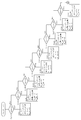
- step S13 The figure which shows the waveform example of the two-phase PWM pulse corresponding to the pattern (1-11) classified by the process of FIG.
- Flow chart showing processing contents of step S14 (A) is a diagram showing a three-phase PWM signal when the maximum duty is 95%, and (b) when the maximum duty is 105%, and sectors and patterns corresponding to them.
- step S15 The figure which shows the definition of U0, V0, W0 and V0_bai, W0_bai Flowchart showing the processing content of step S16 (part 1) Flowchart showing the processing content of step S16 (part 2) Flowchart showing processing contents of step S17 The figure which shows the example of a change of the two-phase PWM signal corresponding to the process of FIG.
- FIG. 23A is a diagram corresponding to FIG. 23A and is a diagram illustrating patterns (4 to 11).
- FIG. 2 is a diagram illustrating a third detection method (part 1) and illustrating a characteristic PWM signal pattern; 25 equivalent diagram 26 equivalent diagram 16 equivalent view (part 1) 17 equivalent diagram FIG.
- 16 equivalent diagram (2) 22 equivalent diagram The figure which illustrates a 3rd detection system (the 2), and shows the area where an electric current cannot be detected with the motor current waveform detected by the 3rd detection system (the 1)
- the figure which illustrates a characteristic PWM signal pattern The flowchart which shows the process performed following the process shown in FIG.
- the flowchart which shows the process performed following the process shown in FIG. 20 is a flowchart showing processing executed following the processing shown in FIG.
- the flowchart which shows the processing content of a part of step S11 The figure which illustrates a characteristic PWM signal pattern (the 1)
- FIG. 2 is a diagram illustrating a characteristic PWM signal pattern (part 2) The flowchart which shows the processing content of a part of step S9 The figure which illustrates a characteristic PWM signal pattern Diagram showing detected motor current waveform Flow chart illustrating the first and second detection methods, and showing interrupt processing executed for each carrier cycle when performing two-phase modulation.
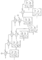
- A is a figure which shows the phase in which a PWM duty pulse is output in the case of two-phase modulation, and the timing at which A / D conversion is performed on the terminal voltage of the resistance element, and (b) is based on orthogonal voltages V ⁇ and V ⁇ .
- FIG. 51 is a figure which shows a sector on an alpha beta coordinate Flowchart showing interrupt processing executed every half of the carrier cycle when performing three-phase modulation Fig. 51
- Vector diagram showing areas where current detection is not possible
- Flow chart showing selection process of current detection method in low speed region
- Flow chart showing the current detection method selection process in the medium speed region
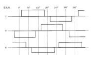
- the figure which shows the PWM signal waveform of the rectangular wave drive system by 120 degrees energization The figure which shows the output voltage waveform of each phase corresponding to FIG.
- FIG. 3 is a flowchart showing an interrupt process that is executed every half of the carrier period when phase modulation is performed.
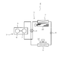
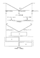
- the compressor (load) 2 constituting the heat pump system 1 is configured by accommodating the compression unit 3 and the motor 4 in the same iron hermetic container 5, and the rotor shaft of the motor 4 is connected to the compression unit 3.
- the compressor 2, the four-way valve 6, the indoor heat exchanger 7, the pressure reducing device 8, and the outdoor heat exchanger 9 are connected by a pipe serving as a heat transfer medium flow path so as to form a closed loop.
- the compressor 2 is, for example, a rotary compressor
- the motor 4 is, for example, a three-phase IPM (Interior Permanent Magnet) motor (brushless DC motor).
- the air conditioner E includes the heat pump system 1 described above.
- the four-way valve 6 is in a state indicated by a solid line during heating, and the high-temperature refrigerant compressed by the compression unit 3 of the compressor 2 is supplied from the four-way valve 6 to the indoor heat exchanger 7 and condensed. Thereafter, the refrigerant is depressurized by the decompression device 8, becomes a low temperature and flows into the outdoor heat exchanger 9, where it evaporates and returns to the compressor 2. On the other hand, at the time of cooling, the four-way valve 6 is switched to a state indicated by a broken line. For this reason, the high-temperature refrigerant
- the refrigerant is depressurized by the decompression device 8, becomes a low temperature and flows into the indoor heat exchanger 7, where it evaporates and returns to the compressor 2.
- the indoor and outdoor heat exchangers 7 and 9 are blown by the fans 10 and 11, respectively, so that the heat exchange between the heat exchangers 7 and 9 and the indoor air and the outdoor air is efficient. It is structured to be performed well.
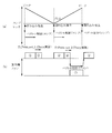
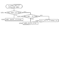
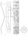
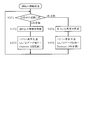
- FIG. 1 is a functional block diagram showing the configuration of the motor control device.
- the DC power supply unit 21 is indicated by a DC power supply symbol, but includes a rectifier circuit, a smoothing capacitor, and the like when a DC power supply is generated from a commercial AC power supply.
- An inverter circuit (DC AC converter) 23 is connected to the DC power supply unit 21 via a positive bus 22a and a negative bus 22b.
- a shunt resistor 24, which is a current detection element, is inserted on the negative bus 22b side.
- the inverter circuit 23 is configured by connecting, for example, N-channel power MOSFETs 25 (U +, V +, W +, U ⁇ , V ⁇ , W ⁇ ) as a switching element in a three-phase bridge connection. Each phase output terminal of the inverter circuit 23 is connected to each phase winding of the motor 4.
- the terminal voltage (signal corresponding to the current value) of the shunt resistor (current detection element) 24 is detected by a current detection unit (current detection unit, timing adjustment unit) 27.
- a current detection unit current detection unit, timing adjustment unit
- the current detection unit 27 performs A / D conversion and reads the terminal voltage
- the current Iu, Iv of each phase of U, V, W is output based on the two-phase or three-phase PWM signal pattern output to the inverter circuit 3.
- Iw is detected.
- Each phase current detected by the current detection unit 27 is input to a vector calculation unit (rotor position determination unit, PWM signal generation unit) 30.
- the torque current command Iqref is calculated based on the difference from the estimated actual rotational speed of the motor 4. Generated.
- the rotor position ⁇ of the motor 4 is determined from the phase currents Iu, Iv, and Iw of the motor 4, and the torque current Iq and the excitation current Id are calculated by vector control calculation using the rotor position ⁇ .
- a PI control calculation is performed to generate a voltage command Vq.
- the excitation current Id side is similarly processed to generate a voltage command Vd.
- the voltage commands Vq, Vd are converted into three-phase voltages Vu, Vv, Vw using the rotor position ⁇ .
- the three-phase voltages Vu, Vv, and Vw are input to a DUTY generation unit (PWM signal generation unit) 31, and duties U_DUTY, V_DUTY, and W_DUTY for generating PWM signals for each phase are determined.
- Each phase duty U, V, W_DUTY is given to the PWM signal generation unit (PWM signal generation unit) 32, and the level with the carrier is compared to generate a two-phase or three-phase PWM signal.
- a signal on the lower arm side is also generated by inverting the two-phase or three-phase PWM signal, and after a dead time is added as necessary, they are output to the drive circuit 33.
- the drive circuit 33 outputs a gate signal to each gate of the six power MOSFETs 25 (U +, V +, W +, U ⁇ , V ⁇ , W ⁇ ) constituting the inverter circuit 23 according to the given PWM signal.
- the gate signal on the upper arm side is output at a potential boosted by a necessary level.
- the vector calculation unit 30 outputs the torque current Iq and the excitation current Id to the power consumption calculation unit 34, calculates the estimated speed ⁇ e based on the torque current Iq, the excitation current Id, and the excitation voltage Vd, and the power consumption calculation unit. 34 and the detection method selection unit 35.
- the power consumption calculation unit 34 outputs the power consumption W to the detection method selection unit (current detection control unit) 35 when the power consumption W is calculated by the following equation based on each input current.
- T a motor output torque
- P the number of poles of the motor 4
- ⁇ an electric winding interlinkage magnetic flux
- Ld a d-axis inductance
- Lq a q-axis inductance.
- the current detection rate calculation unit (current detection rate calculation unit) 36 calculates a current detection rate for each carrier cycle in the current detection unit 27 based on the three-phase voltages Vu, Vv, and Vw input from the vector calculation unit 30. .
- the calculation result is output to the detection method selection unit 35.
- the speed fluctuation detection unit 37 detects the rotational speed of the motor 4 and the degree of speed fluctuation based on the phase current change period output by the current detection unit 27, and outputs the detection result to the detection method selection unit 35.
- the detection method selection unit 35 selects the detection method of the two-phase current in the current detection unit 27 based on the input information. Therefore, the detection method selection unit 35 also outputs a signal for switching between 2-phase modulation and 3-phase modulation to the PWM signal generation unit 32. Further, the PWM signal generation unit 32 outputs a current detection timing signal to the current detection unit 27.
- a rectangular wave drive calculation unit 38 is provided separately from the DUTY generation unit 31 .
- the PWM signal generation unit 32 outputs a 120 ° or 150 ° rectangular wave drive signal input from the rectangular wave drive calculation unit 38 to the drive circuit 33.
- the functions of the configurations 27 to 38 are functions realized by hardware and software of a microcomputer including a CPU.
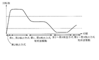
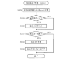
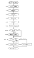
- FIG. 3 shows first to fourth detection methods to be described later for changes in the number of revolutions of the motor 4 built in the compressor 2 and two-phase current detection within the PWM carrier cycle when the cooling operation by the air conditioner is started. The switching state of which one is performed is shown.
- FIG. 4 is a flowchart schematically showing switching of the drive control method corresponding to FIG.
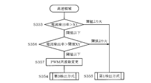
- PWM control is performed with three-phase modulation when the compressor 2 is started to operate the air conditioner (S301). Since the sensorless driving method cannot be executed in the region where the rotational speed of the motor 4 is low, the motor 4 is driven by forced commutation (S302). When the rotational speed increases to some extent, the position sensorless drive method is switched (S303). Thereafter, the detection method of the two-phase current in the current detection unit 27 is selected according to the rotation region (low speed, medium speed, high speed) of the motor 4 and the current detection rate as described later (S304 to S307).
- the rotation speed of the motor 4 is rapidly increased to reach the high speed region in order to rapidly decrease the temperature in the room where the air conditioner is installed.
- the second detection method is executed immediately after startup and while the rotation speed is increased until sensorless driving is possible (S301 to S303), and then the first or third detection method is executed (S307).
- the first or fourth detection method or the rectangular wave driving method is executed (S306).
- one of the first to third detection methods is executed (S305).
- the current detection method is determined according to the level of the rotation speed region of the motor 4 and the level of the current detection rate in each region.
- the threshold value X1 is set at a current detection rate of 90%, and the first detection method is switched to a threshold value X1 or higher, and the third detection method is switched below the threshold value X1.
- the threshold value X2 is set at a current detection rate of 85%, and the threshold is switched to the first detection method when the threshold value is X2 or more and to the fourth detection method when the threshold value is less than the threshold value X2.
- threshold values X3 and X4 are set to current detection rates of 90% and 80%, respectively, the first detection method is greater than or equal to threshold value X3, and the threshold value X4 is less than the third detection method and threshold value X4. If it is less, the second detection method is switched.
- First detection method> This is a general current detection method in two-phase modulation. One-phase current is detected at a fixed timing in the center phase of the carrier cycle, and the other one-phase current is detected at a variable timing according to the change in duty. (Conventional two-phase modulation, see Japanese Patent Application Laid-Open No. 2014-171321).
- ⁇ Third detection method> This is a mixture of two-phase modulation and three-phase modulation.
- one phase of current detection is a fixed timing and the other one phase of current detection is a variable timing.
- Duty pulses are output within the carrier cycle.
- the two phases are based on the center phase of the carrier cycle. Are the second phase and the third phase in which the duty is increased or decreased in the respective directions of the delay side and the advance side.
- a first-phase duty pulse for increasing or decreasing the duty in two directions with respect to the center phase is generated as well as a second value.
- the phase and third phase duty pulses are increased by the predetermined value to switch to three-phase modulation.
- other one-phase current detection that is detected at a fixed timing is also set to a variable timing. Details of this method will be described later.
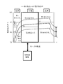
- FIG. 5 shows the current detection rate of the first detection method that has been conventionally performed for two-phase modulation increases and decreases as the motor speed changes. Therefore, an optimum detection method is selected and switched in consideration of power consumption, drive noise, and current detection rate for each rotation speed region.
- FIG. 6 shows the current detection rate by each detection method according to the level of the modulation rate. From the viewpoint of power consumption, it is desirable to employ two-phase modulation as much as possible.
- the current detection rate at the modulation rate corresponding to the medium speed region is higher in the second detection method than in the first detection method.
- the second detection method has a demerit that driving noise becomes larger. Therefore, in the medium speed region, the first detection method is preferentially selected, and the second detection method is selected when the current detection rate decreases.
- the current detection rates of the first and fourth detection methods are both low, and the current detection rates of the second and third detection methods are both 100%. If switching from 2-phase modulation to 3-phase modulation in this region, current detection may become impossible at the switching timing. Therefore, the detection method is selected in the order of first ⁇ third ⁇ second as the current detection rate decreases.
- the current detection rate is higher in the order of 3> 1> 4th. Further, in the high speed region shown in FIG. 5 where the modulation rate exceeds 100%, the current detection rate of the first detection method is lowered. Therefore, the first detection method is preferentially selected from the viewpoint of power consumption, and the third detection method is selected when the current detection rate decreases.
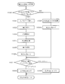
- FIG. 7 is a flowchart showing interrupt processing executed every half cycle of the carrier. That is, a PWM interrupt occurs at the peak and bottom of the triangular wave amplitude that is the carrier.
- S3 the A phase current is detected (S3).
- S3 a “Start F” process described later is executed.
- the A / D conversion processing of the terminal voltage of the shunt resistor 24 in the current detection unit 27 is executed twice within one carrier cycle separately from the processing shown in FIG. 3 (execution timing will be described later).
- the A / D converted data is stored in, for example, a register. Therefore, the process of step S2 reads the data stored in the register.
- the rotor position ( ⁇ ) of the motor 4 is estimated from the three-phase current by vector control calculation (S4), and frequency control (speed control, S5) and current control (PI control, etc.) are executed (S6). Then, the flag M_INT_flg is set to “1” (S7). The subsequent steps S8 to S10 are performed in the DUTY generation unit 31. With reference to the value of the carrier counter supplied from the PWM signal generation unit 32, it is determined whether the up-counting or down-counting is in progress (S8). If up-counting is in progress, D_Pwm_set_2 () is set (S9), and if down-counting is in progress, D_Pwm_set1_ () is set (S10). These will be described with reference to FIGS.
- step S1 If the flag M_INT_flg is “1 (set)” in step S1, a two-phase PWM signal is output (S11), and the flag M_INT_flg is set to “0” (S12). Then, when the processing of “Start A to E” is executed (S13 to S17), the process proceeds to step S8. That is, in the PWM interrupt process, steps S2 to S8 and S10 are executed in the first half of the cycle, and steps S11 to S17, S8, and S9 are executed in the second half of the cycle.
- FIG. 8 shows an execution time image of interrupt processing at the time of two-phase modulation together with a PWM carrier waveform.
- a motor for driving the fan 11 of the heat exchanger 9 corresponding to the outdoor unit is controlled in parallel with the compressor 2 by a single control circuit (microcomputer).
- the motor that drives the fan 10 of the heat exchanger 7 corresponding to the indoor unit is controlled by another control circuit, a driver IC, or the like.
- FIG. 8 shows processing times (1) to (4) related to motor control of the compressor 2 shown in FIG. 3, and (b) shows processing time related to motor (fan motor) control of the fan 11 ( 5). That is, when a PWM interrupt occurs at the bottom of the triangular wave amplitude, after executing the processing shown in FIG. 3, the motor current is also detected for the fan motor to perform vector control.
- the processes (1) to (4) indicated by circled numbers in the figure the processes (1) and (3) correspond to steps S2 to S8, and the processes (2) and (4) correspond to steps S9 and S10, respectively. It corresponds.
- the fan motor control (5) is performed after the processing (4) is executed.
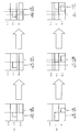
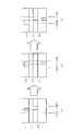
- FIG. 9 shows the output phase of each phase PWM duty pulse.
- the method disclosed in Patent Document 1 is used. That is, in the first phase among the three phases, the duty is increased / decreased in both directions of the delay side and the advance side with reference to the bottom of the triangular wave amplitude.
- the duty is increased or decreased on the leading phase side with respect to the bottom
- the duty is increased or decreased on the delayed phase side with respect to the bottom.
- the first, second, and third phases are the U, V, and W phases, respectively, but these correspondences are of course arbitrary.
- the carrier counter When an interrupt occurs at the peak of the triangular wave amplitude, the carrier counter is counting down, so the duty pulse of the first half of the current carrier cycle is output by D_Pwm_set_2 (). Note that the duty values of the U, V, and W phases are twice the duty values (U0, V0, and W0 described later) calculated in step S11.
- a pulse with half the duty is output from the timing after the interrupt at the peak to the bottom.
- the pulse is output in the period from the timing after the interruption at the peak to the bottom as in the U phase.
- the duty exceeds 50%, the excess pulses are output during the period from when the interrupt at the peak occurs until the bottom is reached. Therefore, it is these pulses that are output by D_Pwm_set_2 ().
- the carrier counter is counting up, so the D_Pwm_set_1 () outputs a duty pulse for the latter half of the current carrier cycle.
- a pulse having a duty of 1/2 is output in the period from the timing to the peak after the interruption at the bottom occurs.
- the duty exceeds 50%
- the excess pulses are output during the period from the timing when the interruption at the bottom occurs until the peak is reached.
- the W phase if the duty is less than 50%, the pulse is output in the period from the timing to the peak after the bottom interruption occurs, as in the U phase. Therefore, it is these pulses that are output by D_Pwm_set_1 ().
- FIG. 9 shows three-phase duty pulses, since the actual drive format is two-phase modulation, only two-phase duty pulses are output.
- the process (Start A) in step S13 will be described.
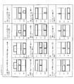
- the patterns are classified into patterns (0) to (11) according to the magnitude relationship of the respective phase duty pulses in the two-phase modulation PWM signal. These patterns are indicated by a variable ptn in the processing described later.
- the pattern division here is based on the following conditions.
- the current detection unit 27 sets a minimum duty that can be detected as a minimum width, and a maximum width (100%) obtained by subtracting the minimum width as a maximum width. For example, if the minimum time during which current can be detected is 10 ⁇ s and the carrier frequency is 4 kHz, the minimum width is 4% and the maximum width is 96%. If the duty that is less than the maximum width and exceeds the minimum width is an intermediate width, the output pattern of the two-phase PWM signal is divided into patterns according to the following combinations of U, V, and W phase duties.
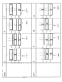
- FIG. 11 shows two-phase PWM signal patterns corresponding to patterns (1) to (11).
- patterns (4) to (11) correspond to an overmodulation state in which the output voltage is extremely large.
- the pattern (7) is shown when the W-phase duty is less than the minimum width.
- step S14 the process (Start B) in step S14 will be described.
- the sectors (0) to (5) are classified according to the relative magnitude relationship of the duty pulses of each phase in the PWM signal of two-phase modulation. These sectors are indicated by a variable sector in the processing described later.
- the sector division here is based on the following conditions. (0) U phase is maximum and V phase> W phase (1) U phase is maximum and V phase ⁇ W phase (2) V phase is maximum and U phase> W phase (3) V phase is maximum And U phase ⁇ W phase (4) W phase is maximum and U phase> V phase (5) W phase is maximum and U phase ⁇ V phase
- FIG. 13 shows sectors and patterns that change according to the actual output of a PWM signal.
- A is the case where the maximum duty is 95%, which is near the maximum width, the sector changes from (0) to (5), and the pattern changes from (0) to (3), (8) to (10). is doing.
- B is the case where the maximum duty exceeds 105% (overmodulation state), the sector changes from (0) to (5), but the pattern changes from (0) to (9). ing. That is, as the output voltage increases, the time span occupied by the patterns (0) to (3) is expanded, and the section where the patterns (4) to (11) are generated at the boundary where the patterns (0) to (3) are switched. It can be seen that is increasing.
- step S15 the current detection unit 27 determines the timing for A / D conversion of the terminal voltage of the shunt resistor 24 within the carrier period in accordance with the combination of the pattern and the sector.
- ⁇ in the figure is set in consideration of the above-described current detectable time, current detection accuracy, and the like (for example, duty 5 to 10%).
- PWM_MAX is the maximum value of duty: 100%.
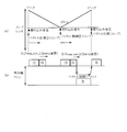
- U0, V0, and W0 in the figure correspond to 1/2 of the U, V, and W-phase duties that are initially determined with the intermediate point (bottom) of the carrier cycle as the base point, as shown in FIG. 15 (a). It is time to do.
- V0_bai and W0_bai are intermediate points of the carrier cycle when the V and W phase duty pulses are shifted in order to output the three-phase PWM signal in the pattern shown in FIG. This corresponds to the length of the pulse extending from the base point.
- Time is a variable indicating the A / D conversion timing of each phase of U, V, and W.
- Step S53 is the case of pattern (1) and sector (2), and the A / D conversion timing is set to (PWM_MAX- ⁇ ).
- Step S54 is the case of pattern (1) and sector (4), and the A / D conversion timing is set to (PWM_MAX- ⁇ ).
- Step S58 is the case of pattern (3) and sector (3) and overmodulation exceeding V0_bai (PWM_MAX ⁇ 2) (S57: YES), and the A / D conversion timing is set to ⁇ . Yes.
- Step S59 is a case of “NO” in Step S57, and the A / D conversion timing is set to (PWM_MAX ⁇ 2 ⁇ V0_bai + ⁇ ).
- Step S62 is a case of pattern (2) and sector (5), and a case of overmodulation in which W0_bai exceeds (PWM_MAX ⁇ 2) (S61: YES), and the A / D conversion timing is set to ⁇ . Yes.
- Step S63 is the case of “NO” in Step S61, and the A / D conversion timing is set to (PWM_MAX ⁇ 2 ⁇ W0_bai + ⁇ ).
- step S16 the process (Start D) in step S16 will be described.
- the timing at which the current detection unit 27 performs A / D conversion within the carrier period is reduced from the beginning (peak) to the half period (bottom) of the carrier period according to the combination of the pattern and the sector.
- the count period and the up-count period from the 1/2 period to the end of the carrier cycle, it is determined at which timing.
- the former is the first detection timing
- the latter is the second detection timing.
- the variable time for setting each timing is the one corresponding to the same combination in StartC.
- the down timing / up count AD timing is set to ⁇ (S72). That is, A / D conversion is performed at the timing when the remaining count value reaches ⁇ from the beginning of the carrier cycle and at the timing when time ⁇ passes from 1 ⁇ 2 of the carrier cycle.
- the U-phase A / D conversion timing is set to time in the up-count period, that is, (PWM_MAX- ⁇ ) determined in step S53. Further, the down-count period is set to ⁇ (S75).
- the up-count period ⁇ is set, and the down-count period is set to time, that is, (PWM_MAX ⁇ ) determined in step S54 ( S77). If the pattern is other than the sector (2-4) (S76: NO), the up-count period and the down-count period are set to ⁇ (S78).
- the up-count period is set to time, that is, ⁇ determined in step S58, or (PWM_MAX ⁇ 2-V0_bai + ⁇ ) determined in step S59. To do.
- the down-count period is set to ⁇ (S81).
- the timing of the up-count period is set to ⁇ . Further, the timing of the downcount period is set to time, that is, (PWM_MAX- ⁇ ) determined in step S60 (S83). If the pattern is (3) and other than sectors (3, 5) (S82: NO), the up-count period and the down-count period are set to ⁇ (S84).
- the timing of the up-count period is set to ⁇ , and the timing of the down-count period is determined to time, that is, determined in step S62.
- ⁇ or (PWM_MAX ⁇ 2-W0_bai + ⁇ ) determined in step S63 is set (S87).
- the timing of the up-count period is set to ⁇ , and the timing of the down-count period is set to ⁇ ⁇ 2 (S85b). If it is the pattern (11) (S85c: YES), the timing of the up count period is set to ⁇ ⁇ 2, and the timing of the down count period is set to ⁇ (S85d). If it is not the pattern (2) and the sector (5) (S86: NO), or if it is not the pattern (11) (S85c: NO), the timing of the up-count period and the down-count period is set to ⁇ , respectively. (S88).
- Step S17 the variable shift used to change the increasing / decreasing direction of the duty pulse is set to any one of “0 to 2” for either the second phase (V) or the third phase (W). .
- V-phase duty is greater than or equal to the maximum width and less than 100% (S91: YES)
- W0_bai is obtained by adding the minimum width to the difference obtained by subtracting V0_bai from PWM_MAX (MAX in the figure) ⁇ 2.
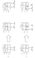
- FIGS. 19A and 19B illustrate the case of pattern (3).
- Pattern (3) is a case where the V-phase duty is greater than or equal to the maximum width and the W-phase duty is greater than or equal to the minimum width.
- a V-phase current is detected at a fixed first detection timing, and a negative U-phase current is detected at a variable second detection timing.
- a negative U phase current is detected. Therefore, the same V-phase current or W-phase current as the first detection timing is detected.
- the direction in which the W-phase duty is increased is changed to the same direction as the V-phase duty.
- the negative U-phase current is detected at the fixed first detection timing
- the V-phase current is detected at the variable second detection timing. Therefore, if the V-phase duty is reduced, the second detection timing may be shifted in the right direction in the drawing to cope with it. Further, even if the W-phase duty is reduced, if the width is equal to or greater than the minimum width, detection can be performed at the fixed first detection timing.
- FIG. 19C shows a case where the variable shift is set to “1” in the case of the pattern (3).
- the arrow with the circled number “1” in the figure indicates the value obtained by adding the minimum width to “the difference obtained by subtracting V0_bai from MAX ⁇ 2 (PWM_MAX ⁇ 2)” in the condition determination in step S92.
- the arrow with “2” indicates W0_bai.
- the variable shift is set to “1” in the case where the left end (variable end) side of the V-phase duty and the right end (variable end) side of the W-phase duty overlap in the up-count section.
- FIG. 19D shows a case where the variable shift is set to “2” in the case of the pattern (2).
- the arrow with the circled number “3” in the figure indicates the value obtained by adding the minimum width to “the difference obtained by subtracting W0_bai from MAX ⁇ 2” in the condition determination in step S96, and the circled number “4” is added.
- the indicated arrow indicates V0_bai.
- the variable shift is set to “2” because, like FIG. 19C, the left end (variable end) side of the V-phase duty and the right end (variable end) side of the W-phase duty in the down-count section are set. This is an overlapping case.
- Step S3 Start F
- the two-phase current is detected within the carrier period based on the combination of the pattern and sector determined in the above processes and the first and second detection timings of the phase current determined by the combination (A / D conversion). Then, a three-phase current is obtained from the detected two-phase current.
- patterns (4) to (11) shown in FIG. 20 are cases of an overmodulation state in which the output voltage of one or more phases is extremely large, and two-phase output is performed within the carrier period. Since it is difficult to detect the current, only the current of one phase is detected.
- the patterns (4), (7), (8), and (10) are down-count timing, and the patterns (5), (6), (9), and (11) are up-count timing, respectively.
- Phase (S102), U phase (S104), V phase (S106), U phase (S108), V phase (S110), W phase (S112), V phase (S114), and W phase (S116) currents are acquired. .
- the current detection timing is ⁇ ⁇ 2.
- step S122 it is determined whether or not it is pattern (1) (step S122). If it is pattern (1) (YES), W and V phase currents are detected at the first and second detection timings ( S123). On the other hand, if it is not the pattern (1) (NO), the W and U phase currents are detected at the first and second detection timings, and the V phase current is obtained by calculation (S124).
- step S125 if it is not the sector (3) in step S125 (NO), as shown in FIG. 22, it is further determined whether it is the sector (4) (S131) or the pattern (1) (S132). In the case of sector (4) and pattern (1) (S132: YES), W and V phase currents are detected at the first and second detection timings (S133). If the pattern is not the pattern (1) (S132: NO), the U and V phase currents are detected at the first and second detection timings (S134).
- step S135 it is determined whether variable shift is “2” (S135).
- the W and U phase currents are detected at the first and second detection timings (S136).
- “NO” it is determined whether or not the pattern is the pattern (2) (S137). If the pattern is the pattern (2) (YES), the U and W phase currents are determined at the first and second detection timings. Is detected (S138). If it is not the pattern (2) (S137: NO), the V and W phase currents are detected at the first and second detection timings (S141).
- FIG. 23 shows the case of pattern (0), and the sector can take all of (0 to 5).
- (B) shows a combination of an actual two-phase modulation PWM signal waveform and a corresponding pattern and sector. Although the phases to be detected are different depending on the sector, the first and second current detection timings are both fixed timings (both down count and up count are ⁇ ).
- FIG. 24 shows the case of pattern (1), and the sector is (2, 4).
- the first and second current detection timings are both fixed timings. However, one is ⁇ and the other is (PMW_MAX ⁇ ).
- FIG. 25 shows the case of pattern (2), and the sector is only (5).
- W0_bai exceeds PWM_MAX ⁇ 2 or shift (2).
- the first and second current detection timings are both fixed.
- W0_bai does not exceed PWM_MAX ⁇ 2
- the first current detection timing is variable, and in the case of shift (2), the V phase duty increase / decrease direction is made the same as the W phase. As a result, the phase to be detected is changed from (U, W) to (W, U).
- FIG. 26 shows the case of pattern (3), and the sector is only (3), but it is further divided into three cases depending on whether V0_bai exceeds PWM_MAX ⁇ 2 or shift (1).
- V0_bai exceeds PWM_MAX ⁇ 2 the first and second current detection timings are both fixed.
- V0_bai does not exceed PWM_MAX ⁇ 2 the second current detection timing is variable, and in the case of shift (1), the W phase duty increase / decrease direction is made the same as the V phase. As a result, the phase to be detected is changed from (V, U) to (U, V).
- FIG. 27 shows patterns (4) to (11) and corresponds to FIG.
- FIG. 28 shows an example of a characteristic change in detection timing in the case of pattern (2) or (3).
- the V and W phase duty pulses are output without a period in which they overlap each other, and the V and W phase currents are detected at the first and second detection timings, respectively.
- the W-phase duty exceeds 96%, a period in which the V and W-phase duty pulses overlap each other occurs in the first half of the carrier cycle. In this case, the phase of the current detected at the first detection timing is changed to the U phase ( ⁇ ).
- the V or W phase duty is reduced from this state, there is a possibility that the U phase current cannot be detected because the V and W phase duty pulses deviate from each other when the first detection timing remains fixed. Therefore, the first detection timing is made variable, and the U-phase current is detected continuously within the overlapping period of the V and W-phase duty pulses.
- FIG. 28 (b) shows a case where a period in which the V and W phase duty pulses overlap each other in the latter half of the carrier cycle due to the V phase duty exceeding 96%.
- the phase of the current detected at the second detection timing is changed to the U phase ( ⁇ ). If the V or W phase duty is reduced from this state, there is a possibility that the U phase current cannot be detected because the V and W phase duty pulses deviate from each other when the second detection timing remains fixed. Therefore, the second detection timing is made variable, and the U-phase current is detected continuously within the overlapping period of the V and W-phase duty pulses.
- FIG. 29 shows an example of a characteristic change in detection timing in the case of pattern (1).
- the period in which the U and V phase duty pulses overlap each other occurs only in the first half of the carrier cycle, and the W ( ⁇ ) and U phase currents are detected at the first and second detection timings, respectively.
- the current detected at the second detection timing is also the W phase ( ⁇ ). Therefore, the second detection timing is changed, and the V-phase current is detected in a period in which only the V-phase duty pulse is generated.
- the second detection timing is fixed at the changed timing (however, it may be variable depending on the change in the V-phase duty).
- FIG. 29 (b) is a case where a period in which the U and W phase duty pulses overlap each other in the first half of the carrier cycle occurs because the W phase duty exceeds 96%.
- the first detection timing is changed, and the W-phase current is detected during a period in which only the W-phase duty pulse is generated.
- the first detection timing is fixed at the changed timing (however, it may be made variable depending on the change in the W-phase duty).
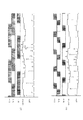
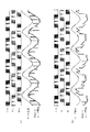
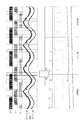
- FIG. 30 shows (a) a motor current waveform detected by the method of the present embodiment and (b) a motor current waveform detected by the method of Patent Document 1 when the modulation factor is approximately 1.0. Is shown. As is apparent from this figure, as a result of the current detection rate being improved in this embodiment, the current waveform is less distorted and closer to a sine wave.
- the current detection unit 27 is configured to operate the motor based on the signal generated by the shunt resistor 24 connected to the DC side of the inverter circuit 23 corresponding to the current value and the PWM signal pattern.
- 4 phase currents Iu, Iv, and Iw are detected, and the vector control unit 30 determines the rotor position ⁇ based on the phase current, and together with the PWM signal generation unit 32, any one of the three phases follows the rotor position ⁇ .
- a two-phase PWM signal pattern is generated.
- the PWM signal generation unit 32 increases or decreases the duty in both directions of the delay side and the advance side with respect to the bottom of the carrier cycle for the U phase of the three-phase PWM signal pattern, and the V phase is based on the bottom.
- the W phase increases or decreases the duty in the direction opposite to the above direction.
- the current detection timing adjustment unit 34 detects the current at a fixed timing for one phase in the two-phase modulation within the carrier cycle, and detects the current at a fixed timing for the other phase.
- the detection timing is adjusted so that the current can be detected at a variable timing corresponding to the magnitude of the output voltage to the inverter circuit 23. Therefore, the current detection rate can be improved even in a region where the output voltage is high and the overmodulation state occurs, and the control accuracy can be improved while suppressing the switching loss.
- the current detection timing adjustment unit 34 determines whether the current detection for the other phase is a predetermined fixed timing or a timing changed from the fixed timing according to the two-phase PWM signal pattern. decide. Specifically, the current detection unit 27 sets the minimum duty that can be detected as the minimum width, determines the maximum width and the intermediate width based on the minimum width, and sets the output pattern of the two-phase PWM signal to any one of the widths. The pattern is divided into patterns (0 to 11) according to the combination of the three-phase duty, and the sector (0 to 5) is classified according to the magnitude relationship of the three-phase duty. Then, depending on the combination of the pattern (0 to 11) and the sector (0 to 5), it is determined whether the current detection for the other phase is set to a predetermined fixed timing or a changed timing. To do.
- the current detection timing adjustment unit 34 sets current detection for the other phase to a predetermined fixed timing, and the two phases in which the duty pulse is output within the carrier cycle are the V and W phases, and both fixed timings.
- the current detection timing adjustment unit 34 may change the period in which the V or W phase duty pulses overlap each other after changing one of the detection target phases to the U phase within a range in which the U phase can be detected. Change the current detection timing. Thereby, it is possible to prevent the repeated change as much as possible while maintaining the changed detection target phase.
- the current detection timing adjustment unit 34 has two phases for which a duty pulse is output within the carrier cycle, the U phase and the V or W phase, and the two-phase current detected at both fixed timings.
- the current detection for the other phase is set as a variable timing, and one of the phases to be detected is set to V or W from the U phase. Change to phase. Therefore, also in this case, the two-phase current can be reliably detected.
- the current detection timing adjustment unit 34 changes the current detection timing for the other phase once, and then fixes the changed timing to detect the V or W phase current. Also in this case, it is possible to prevent the repeated change while maintaining the detection target phase after the change as much as possible.
- the current detection timing adjustment unit 34 is configured such that the two phases for which the duty pulse is output within the carrier cycle are the V and W phases, and when one of these duties decreases, the two-phase current cannot be detected.
- the duty increase / decrease direction of the phase with the smaller duty is changed to the same direction as the other phases. As a result, a period in which the two-phase duty pulses overlap each other is generated, and the two-phase current can be detected.
- the motor 4 which comprises the compressor 2 is controlled about the air conditioner E provided with the heat pump system 1 provided with the compressor 2, the outdoor side heat exchanger 9, the decompression device 8, and the indoor side heat exchanger 7. Since it makes it object, the operating efficiency of the heat pump system 1 and the air conditioner E can be improved.
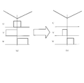
- ⁇ Third detection method (part 1)> In the fourth detection method, for example, as shown in FIG. 26, when the variable shift is “1” in the combination of the pattern (3) and the sector (3), the W phase duty increase / decrease direction is set to the same direction as the V phase. changed. In the third detection method (part 1), different actions are taken for the same case.
- a U-phase duty pulse is also output.
- the V-phase and W-phase duty pulses are increased by the amount of the duty pulse to temporarily enter a three-phase modulation state.
- the first current detection timing is also variable. As a result, the current detection rate is improved without changing the phase to be detected at the second detection timing.
- FIG. 31B corresponds to the case where the variable shift is “2” by the combination of the pattern (2) and the sector (5) shown in FIG. 25 in the description of the fourth detection method.
- a U-phase duty pulse is also output, and the V and W-phase duty pulses are increased by the amount corresponding to the duty pulse to temporarily enter a three-phase modulation state.
- FIGS. 32 and 33 A list including these processing patterns is shown in FIGS. 32 and 33 (corresponding to FIGS. 25 and 26).
- FIG. 34 to 36 are flowcharts of StartD corresponding to FIGS. 16 and 17. However, FIG. 34 shows only steps S71 to S79 in FIG. 16. If “YES” is determined in the step S79, the process proceeds to the process shown in FIG. 35, in the case of the pattern (2) and the sector (5) (S86: YES), it is determined whether or not the variable shift is “0” (S151). If the variable shift is “0” (YES). Step S87 is executed. On the other hand, if the variable shift is not “0” (NO), the first and second detection timings are set to a value obtained by adding ⁇ to the U-phase duty pulse (S152).
- FIG. 36 in the case of pattern (3) and sector (3) (S80: YES), it is determined whether or not the variable shift is “0” (S153), and if the variable shift is “0” (YES). Step S81 is executed. On the other hand, if the variable shift is not “0” (NO), the process is the same as S152 (S154). Also in the case of pattern (3) and sector (5) (S82: YES), it is determined whether or not the variable shift is “0” (S157). If the variable shift is “0” (YES), step S83. Execute. On the other hand, if the variable shift is not “0” (NO), the process is the same as S152 (S156).
- FIG. 37 is a diagram corresponding to FIG. 22 and is a part of the StartF process.
- the current detection timing adjustment unit 34 uses the current detection for the other phase as a variable timing, and the two phases for which the duty pulse is output within the carrier cycle are V
- the U-phase duty pulse is generated by a predetermined value, and the V- and W-phase duty pulses are generated. Is increased by the predetermined value.
- the current detection for one phase is also made variable timing. Thereby, a current detection rate can be improved.
- FIG. 40 shows a process (StartA +) executed after the flowchart of StartA shown in FIG. 10 is executed.
- the patterns are classified into patterns (0) to (5) indicated by the variable Ptn_3phs_ch according to the magnitude relationship of the duty pulses of the phases in the PWM signal of the two-phase modulation.
- the pattern division here is based on the following conditions.
- the minimum duty at which the current detection unit 27 can detect current is set as the minimum width, and the minimum width obtained by subtracting the minimum width from the maximum duty (100%) is set as the maximum width. For example, if the minimum time during which current can be detected is 10 ⁇ s and the carrier frequency is 4 kHz, the minimum width is 4% and the maximum width is 96%.
- the output pattern of the two-phase PWM signal is divided into patterns according to the following combinations of U, V, and W phase duties.
- U0bai_2, V0bai_2, and W0bai_2 are twice the duty values of the U, V, and W phases during the two-phase modulation calculated in step S11.
- W0bai_2 is less than maximum width or V0bai_2 is less than maximum width and U0bai_2 / 2 or V0bai_2 or W0bai_2 is less than minimum width and 0 or more
- W0bai_2 is more than maximum width or V0bai_2 is more than maximum width and U0bai_2 1/2 is less than the minimum width and V0bai_2 is less than the minimum width and 0 or more.
- W0bai_2 is more than the maximum width or V0bai_2 is more than the maximum width and 1/2 of U0bai_2 is more than the minimum width and W0bai_2 Is less than the minimum width and greater than or equal to 0.
- W0bai_2 is greater than or equal to the maximum width or V0bai_2 is greater than or equal to the maximum width and U0bai_2 is less than the minimum width and greater than or equal to 0 and V0bai_2 is greater than W0bai_2. Is greater than the maximum width or V0bai_2 is greater than the maximum width, 1/2 of U0bai_2 is less than the minimum width and greater than 0, and V0bai_2 is less than W0bai_2 (0) Other than the above Pattern (0) to (5); Variable Ptn We have separated the 3phs_ch.
- FIG. 41 is a process (StartD +) that is shifted to after the execution of step S88 in the flowchart of StartD shown in FIGS. 16 and 17, and the AD timing at the time of up-counting and down-counting is determined according to the variable Ptn_3phs_ch. .
- Ptn_3phs_ch is (2) to (5)
- the current detection timing is set to ⁇ ⁇ 3 during up-counting and down-counting (S172, S174) at the timing when the PWM pulse for one phase is ON. This is for detecting the current, and the magnification may be another value, for example, twice.
- the fixed timing ⁇ is set twice (S175).
- FIG. 42 is a process (StartF +) that is shifted to after the execution of step S141 in the flowchart of StartF shown in FIGS. 20 to 22, and two phases for detecting a current are determined according to Ptn_3phs_ch.
- FIG. 43 is a flowchart of PWM output corresponding to step S11.
- the duties U02, V02, and W02 for two-phase modulation are determined.
- Ptn_3phs_ch 0, the minimum of U, V, and W phases is calculated from the respective duty values U0, V0, and W0 calculated by three-phase modulation.
- the duty value Min_Duty is subtracted (S192).
- the U phase which has no pulse output in the two-phase modulation, is output with the pulse width ⁇ ⁇ 2, and the three-phase modulation is performed by adding the pulse width ⁇ ⁇ 2 to the V and W phase pulses. .
- FIG. 45 is a flowchart of a part for determining the U-phase duty value of D_Pwm_set_1 () corresponding to step S10.
- the duty of the V-phase pulse is a large value approaching 100%.
- V-phase current is detected twice during two-phase modulation, but (b) W-phase pulse is added.
- the U-phase pulse is further shifted leftward in the figure (output so as to extend the pulse in the advance direction from the center of the carrier period), and the current detection time is increased. This makes it possible to detect the W-phase current (negative).
- FIG. 47 is a flowchart of a portion for determining the U-phase duty value of D_Pwm_set_2 () corresponding to step S9.
- Ptn_3phs_ch 0 or 1
- the duty value is set to U0bai / 2 (S215).
- FIG. 48 shows a list including these processing patterns.
- FIG. 49 shows the waveform of the motor current detected by the third detection method (part 2). As is apparent from this figure, as a result of the current detection rate being improved by the three-phase modulation, the current waveform is less distorted and close to a sine wave.
- the third detection method (part 2), when one of the two-phase pulses in the two-phase modulation cannot be detected due to a decrease in one duty, the remaining one-phase is detected.
- a duty pulse is additionally generated by a predetermined value for three-phase modulation, and the two-phase duty pulse is increased by the predetermined value.
- the three-phase modulation is similarly performed to increase the maximum phase duty, and the PWM pulse The generation base point of the U-phase PWM pulse is shifted according to the magnitude. Thereby, a current detection rate can be improved.
- FIG. 50 is a flowchart showing interrupt processing executed for each carrier cycle when performing two-phase modulation.
- a / D converted data is extracted in the current detector 27 (S311)
- a three-phase current is detected based on the data (S312).
- the A / D conversion processing of the terminal voltage of the shunt resistor 24 in the current detection unit 27 is executed twice within one carrier cycle separately from the processing shown in FIG. 50 (execution timing will be described later).
- the A / D converted data is stored in, for example, a register. Therefore, the processing in step S211 reads the data stored in the register.
- the rotor position ( ⁇ ) of the motor 4 is estimated from the three-phase current by vector control calculation (S313), and frequency control (speed control, S314) and current control (PI control, etc.) are executed (S315).
- S313 vector control calculation
- S314 frequency control
- PI control current control
- S315 current control
- S316 a register, memory or the like
- the two-phase PWM duty obtained here is set in the output register in step S317 of the interrupt processing in the next carrier cycle.
- the two-phase PWM duty determined in the previous carrier cycle is used for output. It is set in the register (S317).
- FIG. 51A shows the phase at which a PWM duty pulse is output in the case of two-phase modulation, and the timing at which the current detector 27 A / D converts the terminal voltage of the shunt resistor 24.
- U and V phase duty pulses are output so that the bottom of the triangular wave is the center phase.
- the first A / D conversion is executed at the bottom timing.
- the current detected at this time is a W-phase negative current.
- the second A / D conversion is executed when a minute time ⁇ that further considers the switching delay has passed after the passage of the time D2 from the bottom.
- the current detected at this time is a U-phase positive current.
- the V-phase current is obtained by calculation based on the above two A / D conversion results.
- FIG. 51B is a table for calculating the two-phase PWM duty based on the orthogonal voltages V ⁇ and V ⁇ obtained in the vector control process.
- sectors 0 to 5 are determined according to the magnitude relationship between the voltages V ⁇ and V ⁇ , and pulse width values D1 and D2 are determined for each sector. Is determined based on the voltages V ⁇ and V ⁇ and the correction value H.
- the correction value H is a term for correcting the duty pulse width in accordance with the DC voltage that is the voltage of the DC power supply unit 21 and is expressed by the following equation.
- H ⁇ 3 ⁇ (PWM register maximum value) ⁇ 32768 / (DC voltage) (2)
- the “PWM register maximum value” is 65535 if the register is 16 bits, for example.
- the PWMa, PWMb and PWMc shown on the right side of FIG. 51 (b) correspond to the three-phase voltages Vu, Vv and Vw output from the vector calculation unit 30 in FIG. It becomes the sum of D1 and D2, or only the pulse width value D2, or “0”.
- FIG. 52 is a flowchart showing interrupt processing executed every half cycle of the carrier cycle when three-phase modulation is performed. Steps S321 to S325 are executed in the same manner as steps S311 to S315 shown in FIG. 50, but in the subsequent step S326, a three-phase PWM duty is output. The subsequent steps S327 to S329 are performed in the DUTY generation unit 31. With reference to the value of the carrier counter provided from the PWM signal generation unit 32, it is determined whether the up-counting or down-counting is in progress (S327). If up-counting is in progress, D_Pwm_set2 () is set (S328), and if down-counting is in progress, D_Pwm_set1 () is set (S329). These will be described with reference to FIGS.
- the two A / D conversion timings in the three-phase modulation are immediately before and after the triangular wave reaches the bottom.
- a W-phase current is obtained at the former timing
- a V-phase current is obtained at the latter timing.
- the former even if A / D conversion is performed at the timing that coincides with the bottom, it is possible to obtain the W-phase current due to the timing of each control, signal delay, and the like.
- FIG. 53 is a diagram corresponding to FIG. 51 (b), but conditions 1 to 3, sectors, D1 and D2 are exactly the same as in the case of two-phase modulation, and only the determined portions of PWMa, PWMb and PWMc are different. . These determinations include not only the pulse width values D1 and D2 but also the maximum value PD of the PWM register described in the explanation of the correction value H.
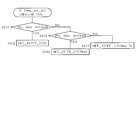
- FIG. 54 is a flowchart showing mainly the control contents executed by the detection method selection unit 36.
- the current detection rate is calculated (S331), and the calculation process is shown in FIG.
- the output duty is calculated for the PWM signal pattern of the first detection method (conventional two-phase modulation) (S334), it is determined whether or not two-phase current can be detected with the obtained duty (S335).
- FIG. 56 is a vector diagram in which current detection impossible periods are indicated by hatching. If the above PWM output duty vector is within the shaded range (for example, when the duty of one phase is around 100% and the duty of the other one phase is around 0%), it is determined that the current cannot be detected. (S335: YES), it counts as a carrier cycle in which current detection is impossible (current detection impossible cycle) (S336). Next, it is determined whether or not one electrical angle cycle has elapsed using the current estimated angle ⁇ Est (S337). When one cycle has elapsed (YES), the current detection rate in that cycle is calculated ( S338).
- S335 YES
- the current detection rate is obtained by the following equation.
- the current rotational speed of the motor 4 and the rotational speed threshold value, or the motor output voltage and the output voltage threshold value are compared, and the currently driven motor 4 rotational speed region (high speed / medium speed / low speed) is determined. judge.
- the output voltage Vm of the motor 4 is calculated as follows using the ⁇ -axis output voltage V ⁇ and the ⁇ -axis output voltage V ⁇ calculated by the vector calculation unit 30.
- Vm ⁇ (V ⁇ 2 + V ⁇ 2) (4)
- the low speed region is, for example, a rotational speed region near the minimum rotational speed
- the high speed region is, for example, a rotational speed region where overmodulation control is effective.
- the medium speed area is a speed area between the high speed area and the low speed area.
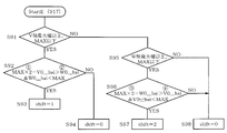
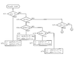
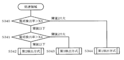
- FIG. 57 is a flowchart of processing for selecting a detection method in the low speed region.
- the current detection rate of the first detection method is compared with the threshold value X3 (S340). If the current detection rate is high (greater than the threshold value), the first detection method is selected (S344), and if the current detection rate is low ( The current detection rate of the first detection method is compared with the threshold value X4 (S341). If the current detection rate is high (greater than the threshold), the third detection method (2-phase + 3-phase modulation) is selected (S343), and if the current detection rate is low (below the threshold), the second detection method (new 3-phase modulation) is selected. Select (S342).
- the current detection rate of the first detection method tends to decrease, but it is preferable to adopt the first detection method in order to reduce power consumption. Therefore, when the current detection rate of the first detection method becomes equal to or less than the threshold value X3, the third detection method is selected to improve the current detection rate. Further, when the current detection rate of the third detection method becomes equal to or less than the threshold value X4, the second detection method is selected to improve the current detection rate again.
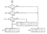
- FIG. 58 is a flowchart of processing for selecting a detection method in the medium speed region.
- the speed fluctuation detecting unit 37 detects the maximum value and the minimum value of the current estimated speed ⁇ Est during one mechanical angle rotation of the motor 4, and obtains the difference between them as a speed fluctuation width (S345).
- step S347 the above-described speed fluctuation width is compared with the fluctuation width threshold value. If the speed fluctuation width is small (below the threshold value), switching to rectangular wave driving (S348), and if the speed fluctuation width is large (greater than the threshold value), the process proceeds to step S349.
- step S349 the current detection rate of the first detection method is compared with the threshold value X2, and if the current detection rate is high (greater than the threshold value), the first detection method is selected (S351). On the other hand, if the current detection rate is low (below the threshold), the fourth detection method (new two-phase modulation) is selected (S350).
- the modulation rate is higher and the current detection rate is higher than in the low speed region. Therefore, the first detection method is adopted with an emphasis on reducing power consumption. However, the current detection rate is reduced when the motor load is reduced. Is equal to or lower than the threshold value X2, the fourth detection method is selected to improve the current detection rate. If the speed command is constant and the speed fluctuation range is equal to or less than the threshold value, switching to rectangular wave driving is performed to further reduce power consumption.
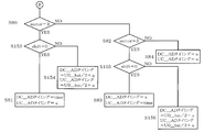
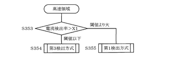
- FIG. 59 is a flowchart of a process for selecting a high-speed area detection method.
- step S353 the current detection rate of the first detection method is compared with the threshold value X1, and if the current detection rate is high (greater than the threshold value), the first detection method is selected (S355), and if the current detection rate is low (below the threshold value). )
- the third detection method is selected (S354).
- the current detection rate of the first detection method is reduced and controllability is deteriorated. Therefore, when the current detection rate of the first detection method becomes equal to or less than the threshold value X1, the third detection method is selected to improve the current detection rate.
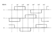
- FIGS. 60 to 63 show the PWM signal waveform and the output voltage waveform in the rectangular wave driving method selected in step S348.
- FIGS. 60 and 61 show the case of the 120 ° energization method in FIG.
- FIG. 63 shows the case of the 150 ° energization method.
- the waveform on the upper side of each phase indicates the ON section of the upper arm
- the waveform on the lower side indicates the ON section of the lower arm. Since the induced voltage of the motor 4 appears in the non-energized section of each phase, the rotor position can be detected by detecting the zero cross point of the induced voltage there. By selecting the rectangular wave driving method in this way, the switching loss is further reduced.
- FIG. 64 is a flowchart schematically showing a modulation method switching process during operation of the air conditioner.
- step S361 if the detection method currently being executed is the first detection method, the process proceeds to step S362, and the cycle for generating the PWM interrupt is set to the same cycle as the carrier cycle. Then, current data is acquired by the first detection method, vector control processing is performed, and a two-phase PWM signal pattern is generated and output (S363).
- step S361 If the currently executed detection method is the second to fourth detection methods, the process proceeds from step S361 to S364, and the cycle for generating the PWM interrupt is set every half cycle of the carrier cycle. Then, current data is acquired by the second to fourth detection methods, vector control processing is performed, and a three-phase PWM signal pattern is generated and output (S365).
- step S361 If the detection method currently being executed is rectangular wave drive control, the process proceeds from step S361 to S366, and the cycle for generating the PWM interrupt is set to the same cycle as the carrier cycle. Then, rectangular wave drive control processing is performed by a position detection method according to rectangular wave drive, and a two-phase PWM signal pattern is generated and output (S367). In the case of rectangular wave driving, it is not necessary to detect a two-phase current for position detection, but only a one-phase current is detected for overcurrent protection.
- the current detection unit 27 is configured so that the motor 4 is based on the signal generated by the shunt resistor 24 connected to the DC side of the inverter circuit 23 corresponding to the current value and the PWM signal pattern.
- the phase calculation unit 30 determines the rotor position ⁇ based on the phase current, and together with the PWM signal generation unit 32, the two-phase or three-phase currents Iu, Iv, Iw are detected. A PWM signal pattern is generated.
- the PWM signal generation unit 32 increases or decreases the duty in either of the delay side and the advance side with respect to the bottom of the carrier cycle with respect to the three-phase PWM signal pattern, Is to increase or decrease the duty in one direction on the delay side and the advance side with respect to the bottom, and in the remaining one phase in the direction opposite to the direction.
- the PWM signal generation unit 32 generates a three-phase PWM signal pattern so that the current detection unit 27 can detect a two-phase current at two fixed or variable timings within the PWM signal carrier cycle. Alternatively, all three phases are output symmetrically from the center of the carrier wave, and a two-phase PWM signal pattern for detecting current at a variable timing is generated. Then, when the motor 4 is in the high speed region, the detection method selection unit 35 selects the first and third detection methods according to the current detection rate in the DUTY generation unit 31 and the PWM signal generation unit 32. Is in the low speed region, one of the first to third detection methods is selected. When the motor 4 is in the medium speed region, the first and fourth detection methods are selected. Thereby, it is possible to improve the control accuracy while suppressing the switching loss while maintaining the necessary current detection rate according to the rotation speed region of the motor 4.
- the detection method selection unit 35 selects a current detection method based on the result of referring to the duty ratio of the PWM signal and the length of the current detectable period within the carrier cycle. Therefore, switching of the PWM signal pattern can be performed appropriately based on the interrupt processing time and the length of the current detectable period.
- the motor 4 which comprises the compressor 2 is controlled object. Therefore, the operation efficiency of the heat pump system 1 and the air conditioner can be improved.
- FIG. 65 is a view corresponding to FIG. 59 showing the second embodiment.
- steps S356 and S357 are inserted between steps S353 and S354. If it is determined in step S353 that it is “below the threshold value”, the current detection rate is compared with a threshold value X1 ′ ( ⁇ X1) (S356).
- the PWM frequency in the PWM signal generation unit 32 is changed to be higher (for example, from 4.5 kHz to 5 kHz) (S357), and the third detection method is executed. (S354).
- the carrier period is adjusted to be shorter. Can be improved.
- FIG. 66 and 67 show the third embodiment, and FIG. 66 corresponds to FIG.
- steps S320, S325a, and S326a are added to the flowchart shown in FIG. 52, and the place where step S326 is executed is changed. That is, when step S325 is executed, the flag M_Int_flg is set to “1” (S325a). The above flag indicates that the processing of steps S321 to S325 has already been executed in the half cycle of the carrier.
- the interrupt processing times (1) and (3) shown in FIG. 66 are slightly shorter than those in the case of processing according to FIG. 52 (corresponding to the case shown in FIG. 8). Since the fan motor control process (5) of the outdoor unit is also executed in the second half of the carrier cycle, the processing time in the second half of the cycle can be provided by dividing the interrupt processing as described above.
- the process of dividing the first half and the second half is not limited to the above example, and may be set as appropriate.
- step S371 of FIG. 68 it is determined whether the modulation method being executed is two-phase modulation or three-phase modulation. In either case, an interrupt is generated every half of the carrier cycle (S372, S374). .
- the two-phase modulation current data is acquired by the corresponding first or fourth detection method, vector control processing is performed, and a two-phase PWM signal pattern is generated and output (S373).
- the three-phase modulation current data is acquired by the corresponding second or third detection method, vector control processing is performed, and a three-phase PWM signal pattern is generated and output (S375).
- FIG. 69 is a diagram corresponding to FIG. 52, but adding steps S326b and S326c between steps S326 and S327 makes the processing common to the two-phase modulation and the three-phase modulation. That is, when step S326 is executed, it is determined whether the modulation method being executed is two-phase or three-phase (S326b), and if it is three-phase modulation (NO), the process proceeds to step S327. On the other hand, in the case of two-phase modulation (YES), the three-phase PWM duty obtained in step S326 is converted into a two-phase PWM duty (S326c), and the process proceeds to step S327.
- two-phase modulation YES
- FIG. 70 illustrates the processing content of step S326c.
- the three-phase PWM duty is obtained as shown in FIG. Among these, the minimum duty is set to MINduty (U phase in this example).
- the two-phase PWM duty is obtained by subtracting (MINduty + ⁇ ) from the duty of the other phases (V, W).
- ⁇ is the dead time equivalent time, but the duty is of course zero for the U phase. Therefore, in this case, the two-phase modulation is performed by the V and W phases.
- the two-phase modulation method can be set at 2 fixed timings as in the three-phase modulation method. The phase current can be detected.
- the PWM interrupt generation pattern is changed in both two-phase modulation and three-phase modulation. It can be said that it is more efficient to create programs.
- the DUTY generating unit 31 when generating the two-phase PWM signal pattern, the DUTY generating unit 31 generates a three-phase PWM signal pattern, and sets the duty of the phase having the smallest duty among these three phases to zero, The two-phase PWM signal pattern is obtained by subtracting the minimum phase duty from the other two-phase duty.
- FIG. 69 it is possible to make the interrupt processing performed by the two-phase modulation and the three-phase modulation as common as possible, and at the two fixed timings in any modulation system, the two-phase modulation is performed. Current can be detected.
- the correspondence between the first to third phases and the U, V, and W phases is arbitrary.
- the carrier period and the minimum width of the PWM duty may be appropriately changed according to individual design.
- the second to third embodiments may be similarly implemented.
- the fourth embodiment is not limited to the one that generates a three-phase PWM pattern and then converts it to a two-phase PWM pattern, but may generate a two-phase PWM pattern as shown in FIG. 51 from the beginning.
- the first to third embodiments of Patent Document 1 may be applied as a method for determining the arrangement of the duty pulses of each phase.
- the power consumption W is not limited to the value calculated by the equation (1), but may be determined by directly measuring the voltage and current.
- the peak of the triangular wave carrier may be the center of the cycle.
- the threshold values X1 to X4 related to the current detection rate may be changed according to individual products.
- the current detection method at the time of motor start-up, forced commutation, and sensorless drive shown in FIGS. 3 and 4 may be the first detection method.
- Embodiments of the present invention provide a control device that controls a motor by PWM controlling an inverter circuit composed of a plurality of switching elements connected in a three-phase bridge, and an air conditioner configured using the motor control device And heat pump systems, and those that control driving of a motor by switching between a two-phase modulation method and a three-phase modulation method.
Abstract
With a motor control apparatus according an embodiment of the present invention, a current detection control unit: sets a first detection scheme wherein a two-phase PWM signal is outputted if a current detection rate is high when the motor is in a low rotation range and wherein a current detection unit detects a current with one phase at fixed timing and the other one phase at variable timing; and that sets a second detection scheme wherein a three-phase PWM signal is outputted when the current detection rate is low and wherein the current detection unit detects the current of two phases at a fixed timing. The current detection control unit sets a third detection scheme wherein, when the current detection rate is in an intermediary state, the two-phase PWM signal is outputted, and wherein, in a state where current detection of one phase is set at a variable timing, two phases with a duty pulse outputted in a carrier wave period are a second phase and a third phase, and when the duty of one of these two phases decreases, making detection of the current of the two phases impossible, a duty pulse of a first phase is generated by a prescribed value, a duty pulse of the second phase and the third phase is increased by the prescribed value, and current detection of the other one phase is also set at a variable timing.
Description
本発明の実施形態は、3相ブリッジ接続された複数のスイッチング素子をPWM制御することで、インバータ回路を介してモータを制御する制御装置,及びその制御装置を備えてなるヒートポンプシステム並びに空気調和機に関する。
Embodiments of the present invention provide a control device that controls a motor via an inverter circuit by PWM-controlling a plurality of switching elements connected in a three-phase bridge, a heat pump system including the control device, and an air conditioner About.
モータを制御するためにU,V,W各相の電流を検出する場合、インバータ回路の直流部に挿入した1つのシャント抵抗を用いて電流検出を行う技術がある。この方式で3相の全ての電流を検出するには、PWM(Pulse Width Modulation,パルス幅変調)キャリア(搬送波)の1周期内において、2相以上の電流を検出できるように3相のPWM信号パターンを発生させる必要がある。そのため、1周期内におけるPWM信号の位相をシフトさせることで常に2相以上の電流を、騒音を増大させること無く検出できるモータ制御装置が提案されている。
When detecting the current of each phase of U, V, W in order to control the motor, there is a technique for detecting the current using one shunt resistor inserted in the DC part of the inverter circuit. To detect all three-phase currents using this method, a three-phase PWM signal can be detected so that two or more phases of current can be detected within one cycle of a PWM (pulse width modulation) carrier (carrier wave). It is necessary to generate a pattern. Therefore, there has been proposed a motor control device that can always detect two or more currents without increasing noise by shifting the phase of the PWM signal within one cycle.
また、3相モータをPWM制御する方式には、3相変調方式と2相変調方式とがある。3相変調方式ではインバータ回路におけるスイッチング損失が増加する。したがって、損失の増加を抑制する観点では2相変調方式を採用するのが望ましい。しかしながら、特許文献1に開示されている電流検出方式を採用すると、モータの低速回転領域では電流の検出が困難になるという問題がある。
Also, there are three-phase modulation method and two-phase modulation method for PWM control of a three-phase motor. In the three-phase modulation method, the switching loss in the inverter circuit increases. Therefore, it is desirable to adopt a two-phase modulation method from the viewpoint of suppressing an increase in loss. However, when the current detection method disclosed in Patent Document 1 is adopted, there is a problem that it becomes difficult to detect current in the low-speed rotation region of the motor.
そこで、スイッチング損失の増加を回避しつつ、1つの電流検出素子による電流検出方式を採用できるモータ制御装置,及びその制御装置を備えてなるヒートポンプシステム並びに空気調和機を提供する。
Therefore, the present invention provides a motor control device that can employ a current detection method using one current detection element while avoiding an increase in switching loss, and a heat pump system and an air conditioner including the control device.
実施形態のモータ制御装置によれば、電流検出部は、インバータ回路の直流側に接続される電流検出素子が電流値に対応して発生した信号とPWM信号パターンとに基づいてモータの相電流を検出し、ロータ位置決定部は、前記相電流に基づいてロータ位置を決定し、PWM信号生成部は、ロータ位置に追従するように2相又は3相のPWM信号パターンを生成する。
According to the motor control apparatus of the embodiment, the current detection unit calculates the phase current of the motor based on the signal generated by the current detection element connected to the DC side of the inverter circuit corresponding to the current value and the PWM signal pattern. Then, the rotor position determination unit determines the rotor position based on the phase current, and the PWM signal generation unit generates a two-phase or three-phase PWM signal pattern so as to follow the rotor position.
電流検出率算出部は、前記2相又は3相のPWM信号パターンに応じて電流検出率を求め、タイミング調整部は、電流検出部がPWM信号の搬送波周期内において、2相の電流を固定されたタイミングで検出するか、又はインバータ回路に対する出力電圧の大きさに応じた可変のタイミングで検出するように調整する。
The current detection rate calculation unit obtains a current detection rate according to the two-phase or three-phase PWM signal pattern, and the timing adjustment unit fixes the two-phase current within the carrier wave period of the PWM signal. Or at a variable timing according to the magnitude of the output voltage to the inverter circuit.
このとき、PWM信号生成部は、3相のPWM信号パターンのうち第1相については、搬送波周期の任意の位相を基準として遅れ側,進み側の双方向にデューティを増減させ、第2相については、搬送波周期の任意の位相を基準として遅れ側,進み側の一方向にデューティを増減させ、第3相については、搬送波周期の任意の位相を基準として前記方向とは逆方向にデューティを増減させるように3相のPWM信号パターンを生成する。
At this time, the PWM signal generation unit increases / decreases the duty in both directions of the delay side and the advance side with respect to the arbitrary phase of the carrier wave period for the first phase of the three-phase PWM signal patterns, and for the second phase. Increases or decreases the duty in one direction of the delay side and the advance side with respect to an arbitrary phase of the carrier wave cycle, and for the third phase, increases or decreases the duty in the opposite direction to the above direction with reference to the arbitrary phase of the carrier wave cycle A three-phase PWM signal pattern is generated so that
そして、電流検出制御部は、モータが低速回転領域にある際に、電流検出率が高い状態では2相のPWM信号パターンを出力させて、電流検出部に1相は固定のタイミングで、他の1相は可変のタイミングで電流を検出させる第1検出方式とし、電流検出率が低い状態では3相のPWM信号パターンを出力させて、電流検出部に固定のタイミングで2相の電流を検出させる第2検出方式とする。
The current detection control unit outputs a two-phase PWM signal pattern in a state where the current detection rate is high when the motor is in a low-speed rotation region, and the current detection unit outputs one phase at a fixed timing. One phase is a first detection method in which current is detected at variable timing. When the current detection rate is low, a three-phase PWM signal pattern is output and the current detection unit detects two-phase current at a fixed timing. The second detection method is used.
また、電流検出率が中間の状態では2相のPWM信号パターンを出力させて、1相の電流検出を可変タイミングとしている状態で、搬送波周期内にデューティパルスが出力されている2相が第2相及び第3相であり、前記2相のうち一方のデューティが減少することで2相の電流が検出できない状態になると、第1相のデューティパルスを所定値だけ発生させると共に、第2相及び第3相のデューティパルスを前記所定値だけ増加させ、且つ他の1相の電流検出も可変タイミングにする第3検出方式とするようにPWM信号生成部及びタイミング調整部を制御する。
Further, in the state where the current detection rate is intermediate, the two-phase PWM signal pattern is output, and the two-phase in which the duty pulse is output within the carrier wave period is the second phase in the state where the one-phase current detection is set as the variable timing. When the current of the two phases is decreased due to a decrease in the duty of one of the two phases, the first phase duty pulse is generated by a predetermined value, and the second phase and the third phase are generated. The PWM signal generation unit and the timing adjustment unit are controlled to increase the third-phase duty pulse by the predetermined value and use the third detection method in which the other one-phase current detection is also variable.
(第1実施形態)
以下、ヒートポンプシステムの一例として、空気調和機の圧縮機モータを駆動する第1実施形態について図1から図64を参照して説明する。図2において、ヒートポンプシステム1を構成する圧縮機(負荷)2は、圧縮部3とモータ4を同一の鉄製密閉容器5内に収容して構成され、モータ4のロータシャフトが圧縮部3に連結されている。そして、圧縮機2、四方弁6、室内側熱交換器7、減圧装置8、室外側熱交換器9は、熱伝達媒体流路たるパイプにより閉ループを構成するように接続されている。尚、圧縮機2は、例えばロータリ型の圧縮機であり、モータ4は、例えば3相IPM(Interior Permanent Magnet)モータ(ブラシレスDCモータ)である。空気調和機Eは、上記のヒートポンプシステム1を有して構成されている。 (First embodiment)
Hereinafter, as an example of a heat pump system, a first embodiment for driving a compressor motor of an air conditioner will be described with reference to FIGS. 1 to 64. In FIG. 2, the compressor (load) 2 constituting theheat pump system 1 is configured by accommodating the compression unit 3 and the motor 4 in the same iron hermetic container 5, and the rotor shaft of the motor 4 is connected to the compression unit 3. Has been. The compressor 2, the four-way valve 6, the indoor heat exchanger 7, the pressure reducing device 8, and the outdoor heat exchanger 9 are connected by a pipe serving as a heat transfer medium flow path so as to form a closed loop. The compressor 2 is, for example, a rotary compressor, and the motor 4 is, for example, a three-phase IPM (Interior Permanent Magnet) motor (brushless DC motor). The air conditioner E includes the heat pump system 1 described above.
以下、ヒートポンプシステムの一例として、空気調和機の圧縮機モータを駆動する第1実施形態について図1から図64を参照して説明する。図2において、ヒートポンプシステム1を構成する圧縮機(負荷)2は、圧縮部3とモータ4を同一の鉄製密閉容器5内に収容して構成され、モータ4のロータシャフトが圧縮部3に連結されている。そして、圧縮機2、四方弁6、室内側熱交換器7、減圧装置8、室外側熱交換器9は、熱伝達媒体流路たるパイプにより閉ループを構成するように接続されている。尚、圧縮機2は、例えばロータリ型の圧縮機であり、モータ4は、例えば3相IPM(Interior Permanent Magnet)モータ(ブラシレスDCモータ)である。空気調和機Eは、上記のヒートポンプシステム1を有して構成されている。 (First embodiment)
Hereinafter, as an example of a heat pump system, a first embodiment for driving a compressor motor of an air conditioner will be described with reference to FIGS. 1 to 64. In FIG. 2, the compressor (load) 2 constituting the
四方弁6は、暖房時には実線で示す状態にあり、圧縮機2の圧縮部3で圧縮された高温冷媒は、四方弁6から室内側熱交換器7に供給されて凝縮される。その後、冷媒は減圧装置8で減圧され、低温となって室外側熱交換器9に流れ、ここで蒸発して圧縮機2へと戻る。一方、冷房時には、四方弁6は破線で示す状態に切り替えられる。このため、圧縮機2の圧縮部3で圧縮された高温冷媒は、四方弁6から室外側熱交換器9に供給されて凝縮される。その後、冷媒は減圧装置8で減圧され、低温となって室内側熱交換器7に流れ、ここで蒸発して圧縮機2へと戻る。そして、室内側、室外側の各熱交換器7,9には、それぞれファン10,11により送風が行われ、その送風により各熱交換器7,9と室内空気、室外空気の熱交換が効率良く行われるように構成されている。
The four-way valve 6 is in a state indicated by a solid line during heating, and the high-temperature refrigerant compressed by the compression unit 3 of the compressor 2 is supplied from the four-way valve 6 to the indoor heat exchanger 7 and condensed. Thereafter, the refrigerant is depressurized by the decompression device 8, becomes a low temperature and flows into the outdoor heat exchanger 9, where it evaporates and returns to the compressor 2. On the other hand, at the time of cooling, the four-way valve 6 is switched to a state indicated by a broken line. For this reason, the high-temperature refrigerant | coolant compressed by the compression part 3 of the compressor 2 is supplied to the outdoor side heat exchanger 9 from the four-way valve 6, and is condensed. Thereafter, the refrigerant is depressurized by the decompression device 8, becomes a low temperature and flows into the indoor heat exchanger 7, where it evaporates and returns to the compressor 2. The indoor and outdoor heat exchangers 7 and 9 are blown by the fans 10 and 11, respectively, so that the heat exchange between the heat exchangers 7 and 9 and the indoor air and the outdoor air is efficient. It is structured to be performed well.
図1は、モータ制御装置の構成を示す機能ブロック図である。直流電源部21は、直流電源のシンボルで示しているが、商用交流電源から直流電源を生成している場合には、整流回路や平滑コンデンサ等を含んでいる。直流電源部21には、正側母線22a,負側母線22bを介してインバータ回路(直流交流変換器)23が接続されている。負側母線22b側には電流検出素子であるシャント抵抗24が挿入されている。インバータ回路23は、スイッチング素子として例えばNチャネル型のパワーMOSFET25(U+,V+,W+,U-,V-,W-)を3相ブリッジ接続して構成されている。インバータ回路23の各相出力端子は、それぞれモータ4の各相巻線に接続されている。
FIG. 1 is a functional block diagram showing the configuration of the motor control device. The DC power supply unit 21 is indicated by a DC power supply symbol, but includes a rectifier circuit, a smoothing capacitor, and the like when a DC power supply is generated from a commercial AC power supply. An inverter circuit (DC AC converter) 23 is connected to the DC power supply unit 21 via a positive bus 22a and a negative bus 22b. A shunt resistor 24, which is a current detection element, is inserted on the negative bus 22b side. The inverter circuit 23 is configured by connecting, for example, N-channel power MOSFETs 25 (U +, V +, W +, U−, V−, W−) as a switching element in a three-phase bridge connection. Each phase output terminal of the inverter circuit 23 is connected to each phase winding of the motor 4.
シャント抵抗(電流検出素子)24の端子電圧(電流値に対応した信号)は、電流検出部(電流検出部,タイミング調整部)27により検出される。電流検出部27は、前記端子電圧をA/D変換して読み込むと、インバータ回路3に出力される2相又は3相のPWM信号パターンに基づいてU,V,W各相の電流Iu,Iv,Iwを検出する。電流検出部27が検出した各相電流は、ベクトル演算部(ロータ位置決定部,PWM信号生成部)30に入力される。
The terminal voltage (signal corresponding to the current value) of the shunt resistor (current detection element) 24 is detected by a current detection unit (current detection unit, timing adjustment unit) 27. When the current detection unit 27 performs A / D conversion and reads the terminal voltage, the current Iu, Iv of each phase of U, V, W is output based on the two-phase or three-phase PWM signal pattern output to the inverter circuit 3. , Iw is detected. Each phase current detected by the current detection unit 27 is input to a vector calculation unit (rotor position determination unit, PWM signal generation unit) 30.
ベクトル演算部30では、制御条件を設定するマイクロコンピュータ等の機能部分よりモータ4の回転速度指令ωrefが与えられると、推定したモータ4の実際の回転速度との差分に基づいてトルク電流指令Iqrefが生成される。モータ4の各相電流Iu,Iv,Iwからはモータ4のロータ位置θが決定され、そのロータ位置θを用いるベクトル制御演算によりトルク電流Iq,励磁電流Idが算出される。
In the vector calculation unit 30, when the rotational speed command ωref of the motor 4 is given from a functional part such as a microcomputer that sets the control conditions, the torque current command Iqref is calculated based on the difference from the estimated actual rotational speed of the motor 4. Generated. The rotor position θ of the motor 4 is determined from the phase currents Iu, Iv, and Iw of the motor 4, and the torque current Iq and the excitation current Id are calculated by vector control calculation using the rotor position θ.
トルク電流指令Iqrefとトルク電流Iqとの差分に対しては、例えばPI制御演算が行われて電圧指令Vqが生成される。励磁電流Id側についても同様に処理されて電圧指令Vdが生成される。電圧指令Vq,Vdは、上記ロータ位置θを用いて三相電圧Vu,Vv,Vwに変換される。三相電圧Vu,Vv,Vwは、DUTY生成部(PWM信号生成部)31に入力され、各相のPWM信号を生成するためのデューティU_DUTY,V_DUTY,W_DUTYが決定される。
For the difference between the torque current command Iqref and the torque current Iq, for example, a PI control calculation is performed to generate a voltage command Vq. The excitation current Id side is similarly processed to generate a voltage command Vd. The voltage commands Vq, Vd are converted into three-phase voltages Vu, Vv, Vw using the rotor position θ. The three-phase voltages Vu, Vv, and Vw are input to a DUTY generation unit (PWM signal generation unit) 31, and duties U_DUTY, V_DUTY, and W_DUTY for generating PWM signals for each phase are determined.
各相デューティU,V,W_DUTYは、PWM信号生成部(PWM信号生成部)32に与えられ、キャリアとのレベルが比較されて2相又は3相PWM信号が生成される。また、2相又は3相PWM信号を反転させて下アーム側の信号も生成され、必要に応じてデッドタイムが付加された後、それらが駆動回路33に出力される。駆動回路33は、与えられたPWM信号に従い、インバータ回路23を構成する6つのパワーMOSFET25(U+,V+,W+,U-,V-,W-)の各ゲートにゲート信号を出力する。この時上アーム側のゲート信号については、必要なレベルだけ昇圧した電位で出力する。PWM信号生成部31が3相PWM信号を生成する方式については、例えば特許文献1に開示がある第4実施形態の方式を用いる。
Each phase duty U, V, W_DUTY is given to the PWM signal generation unit (PWM signal generation unit) 32, and the level with the carrier is compared to generate a two-phase or three-phase PWM signal. In addition, a signal on the lower arm side is also generated by inverting the two-phase or three-phase PWM signal, and after a dead time is added as necessary, they are output to the drive circuit 33. The drive circuit 33 outputs a gate signal to each gate of the six power MOSFETs 25 (U +, V +, W +, U−, V−, W−) constituting the inverter circuit 23 according to the given PWM signal. At this time, the gate signal on the upper arm side is output at a potential boosted by a necessary level. As a method in which the PWM signal generation unit 31 generates a three-phase PWM signal, for example, the method of the fourth embodiment disclosed in Patent Document 1 is used.
その他、ベクトル演算部30は、トルク電流Iq及び励磁電流Idを消費電力演算部34に出力し、トルク電流Iq,励磁電流Id及び励磁電圧Vdに基づいて推定速度ωeを演算し、消費電力演算部34及び検出方式選択部35に出力する。消費電力演算部34は、入力される各電流に基づいて消費電力Wを次式により演算すると、検出方式選択部(電流検出制御部)35に出力する。
In addition, the vector calculation unit 30 outputs the torque current Iq and the excitation current Id to the power consumption calculation unit 34, calculates the estimated speed ωe based on the torque current Iq, the excitation current Id, and the excitation voltage Vd, and the power consumption calculation unit. 34 and the detection method selection unit 35. The power consumption calculation unit 34 outputs the power consumption W to the detection method selection unit (current detection control unit) 35 when the power consumption W is calculated by the following equation based on each input current.
W=ωe×T=ωe×P/2×{φ×Iq+(Ld-Lq)}×Id×Iq…(1)
但し、Tはモータ出力トルク,Pはモータ4の極数,φは電気子巻線鎖交磁束,Ldはd軸インダクタンス,Lqはq軸インダクタンスである。尚、消費電力演算部34については、第3実施形態で説明する。 W = ωe × T = ωe × P / 2 × {φ × Iq + (Ld−Lq)} × Id × Iq (1)
However, T is a motor output torque, P is the number of poles of themotor 4, φ is an electric winding interlinkage magnetic flux, Ld is a d-axis inductance, and Lq is a q-axis inductance. The power consumption calculation unit 34 will be described in the third embodiment.
但し、Tはモータ出力トルク,Pはモータ4の極数,φは電気子巻線鎖交磁束,Ldはd軸インダクタンス,Lqはq軸インダクタンスである。尚、消費電力演算部34については、第3実施形態で説明する。 W = ωe × T = ωe × P / 2 × {φ × Iq + (Ld−Lq)} × Id × Iq (1)
However, T is a motor output torque, P is the number of poles of the
電流検出率算出部(電流検出率算出部)36は、ベクトル演算部30より入力される三相電圧Vu,Vv,Vwに基づいて、電流検出部27におけるキャリア周期毎の電流検出率を算出する。その算出結果は、検出方式選択部35に出力される。速度変動検出部37は、電流検出部27が出力する相電流の変化周期に基づいて、モータ4の回転速度及び速度の変動度合いを検出し、検出結果を検出方式選択部35に出力する。検出方式選択部35は、これらの入力情報に基づいて、電流検出部27における2相の電流の検出方式を選択する。そのため、検出方式選択部35は、PWM信号生成部32に対しても、2相変調/3相変調を切替えるための信号を出力する。また、PWM信号生成部32からは、電流検出部27に対して電流検出タイミング信号が出力される。
The current detection rate calculation unit (current detection rate calculation unit) 36 calculates a current detection rate for each carrier cycle in the current detection unit 27 based on the three-phase voltages Vu, Vv, and Vw input from the vector calculation unit 30. . The calculation result is output to the detection method selection unit 35. The speed fluctuation detection unit 37 detects the rotational speed of the motor 4 and the degree of speed fluctuation based on the phase current change period output by the current detection unit 27, and outputs the detection result to the detection method selection unit 35. The detection method selection unit 35 selects the detection method of the two-phase current in the current detection unit 27 based on the input information. Therefore, the detection method selection unit 35 also outputs a signal for switching between 2-phase modulation and 3-phase modulation to the PWM signal generation unit 32. Further, the PWM signal generation unit 32 outputs a current detection timing signal to the current detection unit 27.
また、DUTY生成部31とは別個に、矩形波駆動演算部38が設けられている。PWM信号生成部32は、後述する特定の速度領域においてモータ4の回転速度が安定すると、矩形波駆動演算部38より入力される120°又は150°矩形波の駆動信号を駆動回路33に出力する。尚、以上において、構成27~38(駆動回路33を除く)の機能は、CPUを含むマイクロコンピュータのハードウェア及びソフトウェアにより実現される機能である。
Further, separately from the DUTY generation unit 31, a rectangular wave drive calculation unit 38 is provided. When the rotational speed of the motor 4 is stabilized in a specific speed region to be described later, the PWM signal generation unit 32 outputs a 120 ° or 150 ° rectangular wave drive signal input from the rectangular wave drive calculation unit 38 to the drive circuit 33. . In the above description, the functions of the configurations 27 to 38 (excluding the drive circuit 33) are functions realized by hardware and software of a microcomputer including a CPU.
次に、本実施形態の作用について図3から図64を参照して説明する。図3は、エアコンによる冷房運転を開始させた場合の、圧縮機2に内蔵されるモータ4の回転数の変化と、PWMキャリア周期内における2相電流検出を後述する第1~第4検出方式の何れで行うかの切り換え状態を示している。また、図4は、図3に対応した駆動制御方式の切り換えを概略的に示すフローチャートである。
Next, the operation of this embodiment will be described with reference to FIGS. FIG. 3 shows first to fourth detection methods to be described later for changes in the number of revolutions of the motor 4 built in the compressor 2 and two-phase current detection within the PWM carrier cycle when the cooling operation by the air conditioner is started. The switching state of which one is performed is shown. FIG. 4 is a flowchart schematically showing switching of the drive control method corresponding to FIG.
図4に示すように、エアコンの運転が開始された圧縮機2の起動時には、3相変調でPWM制御を行う(S301)。モータ4の回転数が低い領域ではセンサレス駆動方式が実行できないため、強制転流によりモータ4を駆動する(S302)。そして、回転数がある程度上昇すると位置センサレス駆動方式に切り換える(S303)。その後は、モータ4の回転領域(低速,中速,高速),及び後述するように電流検出率に応じて、電流検出部27における2相の電流の検出方式を選択する(S304~S307)。
As shown in FIG. 4, PWM control is performed with three-phase modulation when the compressor 2 is started to operate the air conditioner (S301). Since the sensorless driving method cannot be executed in the region where the rotational speed of the motor 4 is low, the motor 4 is driven by forced commutation (S302). When the rotational speed increases to some extent, the position sensorless drive method is switched (S303). Thereafter, the detection method of the two-phase current in the current detection unit 27 is selected according to the rotation region (low speed, medium speed, high speed) of the motor 4 and the current detection rate as described later (S304 to S307).
図3に示すように、エアコンの運転開始直後は、エアコンが設置されている部屋内の温度を迅速に低下させるためモータ4の回転数を急激に上昇させて高速領域に至る。この場合、起動直後及びセンサレス駆動が可能になるまで回転数を上昇させる間は第2検出方式を実行し(S301~S303)、その後に第1又は第3検出方式を実行する(S307)。運転開始直後に急激に出力を上昇させたことで室内温度が低下すると、モータ4の回転数を低下させて中速領域に至る。この場合は第1若しくは第4検出方式又は矩形波駆動方式を実行する(S306)。そして、室内温度が安定して低速領域に至ると、第1~第3検出方式の何れかを実行する(S305)。
As shown in FIG. 3, immediately after the start of the operation of the air conditioner, the rotation speed of the motor 4 is rapidly increased to reach the high speed region in order to rapidly decrease the temperature in the room where the air conditioner is installed. In this case, the second detection method is executed immediately after startup and while the rotation speed is increased until sensorless driving is possible (S301 to S303), and then the first or third detection method is executed (S307). When the room temperature decreases due to a sudden increase in output immediately after the start of operation, the number of rotations of the motor 4 is decreased to reach the middle speed region. In this case, the first or fourth detection method or the rectangular wave driving method is executed (S306). When the room temperature stabilizes and the low speed region is reached, one of the first to third detection methods is executed (S305).
以降は、上述した電流検出方式の切り換え制御について、より詳細に説明する。電流検出方式は、図5に示すように、モータ4の回転速度領域の高低と、各領域における電流検出率の高低とに応じて決定される。高速領域では、電流検出率90%に閾値X1が設定されており、閾値X1以上では第1検出方式,閾値X1未満では第3検出方式に切り替える。中速領域では、電流検出率85%に閾値X2が設定されており、閾値X2以上では第1検出方式,閾値X2未満では第4検出方式に切り替える。また、中速領域では、前述のようにモータ4の回転速度が安定すると、矩形波駆動方式に切り替える。そして、低速領域では、電流検出率90%,80%にそれぞれ閾値X3,X4が設定されており、閾値X3以上では第1検出方式,閾値X3未満で且つ閾値X4では第3検出方式,閾値X4未満では第2検出方式に切り替える。
Hereinafter, the above-described current detection switching control will be described in more detail. As shown in FIG. 5, the current detection method is determined according to the level of the rotation speed region of the motor 4 and the level of the current detection rate in each region. In the high-speed region, the threshold value X1 is set at a current detection rate of 90%, and the first detection method is switched to a threshold value X1 or higher, and the third detection method is switched below the threshold value X1. In the medium speed region, the threshold value X2 is set at a current detection rate of 85%, and the threshold is switched to the first detection method when the threshold value is X2 or more and to the fourth detection method when the threshold value is less than the threshold value X2. Further, in the medium speed region, when the rotational speed of the motor 4 is stabilized as described above, the rectangular wave driving method is switched. In the low-speed region, threshold values X3 and X4 are set to current detection rates of 90% and 80%, respectively, the first detection method is greater than or equal to threshold value X3, and the threshold value X4 is less than the third detection method and threshold value X4. If it is less, the second detection method is switched.
ここで、第1~第4検出方式について説明する。
<第1検出方式>
一般的な2相変調における電流検出方式であり、1相の電流はキャリア周期の中心位相における固定のタイミングで検出し、他の1相の電流は、デューティの変化に応じた可変のタイミングで検出を行う(従来2相変調,特開2014-171321号公報参照)。 Here, the first to fourth detection methods will be described.
<First detection method>
This is a general current detection method in two-phase modulation. One-phase current is detected at a fixed timing in the center phase of the carrier cycle, and the other one-phase current is detected at a variable timing according to the change in duty. (Conventional two-phase modulation, see Japanese Patent Application Laid-Open No. 2014-171321).
<第2検出方式>
特許文献1に開示されている電流検出方式であり、3相変調において2相の電流共に固定のタイミングで検出する(新3相変調)。 <Second detection method>
This is a current detection method disclosed inPatent Document 1, and two-phase currents are detected at fixed timing in three-phase modulation (new three-phase modulation).
特許文献1に開示されている電流検出方式であり、3相変調において2相の電流共に固定のタイミングで検出する(新3相変調)。 <Second detection method>
This is a current detection method disclosed in
<第3検出方式>
2相変調と3相変調との混合である。2相変調において1相の電流検出を固定タイミングとし、他の1相の電流検出を可変タイミングとしている状態で、キャリア周期内にデューティパルスが出力されている2相がキャリア周期の中心位相を基準として遅れ側,進み側それぞれの方向にデューティを増減させる第2相及び第3相である。これら2相のうち一方のデューティが減少して2相の電流が検出できなくなると、中心位相を基準として双方向にデューティを増減させる第1相のデューティパルスを所定値だけ発生させると共に、第2相及び第3相のデューティパルスを前記所定値だけ増加させて3相変調に切替える。加えて、固定タイミングで検出を行っている他の1相の電流検出も、可変タイミングにする。この方式についての詳細は後述する。 <Third detection method>
This is a mixture of two-phase modulation and three-phase modulation. In two-phase modulation, one phase of current detection is a fixed timing and the other one phase of current detection is a variable timing. Duty pulses are output within the carrier cycle. The two phases are based on the center phase of the carrier cycle. Are the second phase and the third phase in which the duty is increased or decreased in the respective directions of the delay side and the advance side. When one of the two phases decreases and the two-phase current can no longer be detected, a first-phase duty pulse for increasing or decreasing the duty in two directions with respect to the center phase is generated as well as a second value. The phase and third phase duty pulses are increased by the predetermined value to switch to three-phase modulation. In addition, other one-phase current detection that is detected at a fixed timing is also set to a variable timing. Details of this method will be described later.
<第4検出方式>
これについても詳細を後述するが、上記「従来2相変調」に対して「新2相変調」となる方式である。 <Fourth detection method>
Although this will also be described in detail later, this is a “new two-phase modulation” method in contrast to the “conventional two-phase modulation”.
これについても詳細を後述するが、上記「従来2相変調」に対して「新2相変調」となる方式である。 <Fourth detection method>
Although this will also be described in detail later, this is a “new two-phase modulation” method in contrast to the “conventional two-phase modulation”.
図5に示しているように、従来、2相変調について行っている第1検出方式の電流検出率は、モータの回転数が変化するのに応じて増減する。そこで、回転数の領域ごとに消費電力,駆動騒音及び電流検出率を考慮して、最適となる検出方式を選択して切り換える。図6は、変調率の高低に応じた各検出方式により電流検出率を示す。消費電力の観点からは、極力2相変調を採用するのが望ましい。
As shown in FIG. 5, the current detection rate of the first detection method that has been conventionally performed for two-phase modulation increases and decreases as the motor speed changes. Therefore, an optimum detection method is selected and switched in consideration of power consumption, drive noise, and current detection rate for each rotation speed region. FIG. 6 shows the current detection rate by each detection method according to the level of the modulation rate. From the viewpoint of power consumption, it is desirable to employ two-phase modulation as much as possible.
中速領域に対応する変調率での電流検出率は、第2検出方式の方が第1検出方式よりも高くなっている。しかし、第2検出方式は駆動騒音がより大きくなるというデメリットがある。そこで、中速領域では、第1検出方式を優先的に選択し、電流検出率が低下した場合に第2検出方式を選択する。
The current detection rate at the modulation rate corresponding to the medium speed region is higher in the second detection method than in the first detection method. However, the second detection method has a demerit that driving noise becomes larger. Therefore, in the medium speed region, the first detection method is preferentially selected, and the second detection method is selected when the current detection rate decreases.
低速領域に対応する変調率では、第1及び第4検出方式の電流検出率は何れも低く、第2及び第3検出方式の電流検出率は何れも100%である。この領域で2相変調から3相変調に切替えると、その切り換えのタイミングで電流検出が不能になるおそれがある。そこで、電流検出率が低下するのに応じて、第1→第3→第2の順で検出方式を選択する。
At the modulation rate corresponding to the low speed region, the current detection rates of the first and fourth detection methods are both low, and the current detection rates of the second and third detection methods are both 100%. If switching from 2-phase modulation to 3-phase modulation in this region, current detection may become impossible at the switching timing. Therefore, the detection method is selected in the order of first → third → second as the current detection rate decreases.
そして、変調率が100%付近の領域では、第3>第1>第4の順で電流検出率が高い。また、変調率が100%を超える図5に示す高速領域では、第1検出方式の電流検出率が低下する。したがって、第1検出方式を消費電力の観点から優先的に選択し、電流検出率が低下した場合に第3検出方式を選択する。
In the region where the modulation rate is near 100%, the current detection rate is higher in the order of 3> 1> 4th. Further, in the high speed region shown in FIG. 5 where the modulation rate exceeds 100%, the current detection rate of the first detection method is lowered. Therefore, the first detection method is preferentially selected from the viewpoint of power consumption, and the third detection method is selected when the current detection rate decreases.
以降では、第3及び第4検出方式について説明するが、先に第4検出方式について説明する。
<第4検出方式>
図7は、キャリアの半周期毎に実行される割り込み処理を示すフローチャートである。すなわち、キャリアである三角波振幅のピークとボトムとにおいてPWM割り込みが発生する。先ず、フラグM_INT_flg=0(リセット)か否かを判断し(S1)、「0」であれば電流検出部27においてA/D変換されたデータを抽出すると(S2)、そのデータに基づいて3相電流を検出する(S3)。尚、ステップS3では、後述する「StartF」の処理が実行される。 Hereinafter, although the third and fourth detection methods will be described, the fourth detection method will be described first.
<Fourth detection method>
FIG. 7 is a flowchart showing interrupt processing executed every half cycle of the carrier. That is, a PWM interrupt occurs at the peak and bottom of the triangular wave amplitude that is the carrier. First, it is determined whether or not the flag M_INT_flg = 0 (reset) (S1). If “0”, the A / D converted data is extracted by the current detection unit 27 (S2). A phase current is detected (S3). In step S3, a “Start F” process described later is executed.
ここで、電流検出部27におけるシャント抵抗24の端子電圧のA/D変換処理は、図3に示す処理とは別個に1キャリア周期内で2回実行されており(実行タイミングについては後述する)、A/D変換されたデータは、例えばレジスタ等に格納されている。したがって、ステップS2の処理は、上記レジスタに格納されているデータを読み出すことになる。
Here, the A / D conversion processing of the terminal voltage of the shunt resistor 24 in the current detection unit 27 is executed twice within one carrier cycle separately from the processing shown in FIG. 3 (execution timing will be described later). The A / D converted data is stored in, for example, a register. Therefore, the process of step S2 reads the data stored in the register.
次に、3相電流からベクトル制御演算によりモータ4のロータ位置(θ)を推定し(S4)、周波数制御(速度制御,S5)及び電流制御(PI制御等)を実行する(S6)。それから、フラグM_INT_flgを「1」にする(S7)。続くステップS8~S10の処理は、DUTY生成部31において行われる。PWM信号生成部32より与えられるキャリアカウンタの値を参照し、アップカウント中か、ダウンカウント中かを判断する(S8)。アップカウント中であればD_Pwm_set_2()をセットし(S9)、ダウンカウント中であればD_Pwm_set1_()をセットする(S10)。これらについては図8及び図9を参照して説明する。
Next, the rotor position (θ) of the motor 4 is estimated from the three-phase current by vector control calculation (S4), and frequency control (speed control, S5) and current control (PI control, etc.) are executed (S6). Then, the flag M_INT_flg is set to “1” (S7). The subsequent steps S8 to S10 are performed in the DUTY generation unit 31. With reference to the value of the carrier counter supplied from the PWM signal generation unit 32, it is determined whether the up-counting or down-counting is in progress (S8). If up-counting is in progress, D_Pwm_set_2 () is set (S9), and if down-counting is in progress, D_Pwm_set1_ () is set (S10). These will be described with reference to FIGS.
また、ステップS1でフラグM_INT_flgが「1(セット)」であれば(NO)2相のPWM信号を出力し(S11)、フラグM_INT_flgを「0」にする(S12)。それから、「StartA~E」の処理が実行されると(S13~S17)、ステップS8に移行する。つまり、上記のPWM割り込み処理では、周期の前半でステップS2~S8,S10を実行し、周期の後半でステップS11~S17,S8,S9を実行することになる。
If the flag M_INT_flg is “1 (set)” in step S1, a two-phase PWM signal is output (S11), and the flag M_INT_flg is set to “0” (S12). Then, when the processing of “Start A to E” is executed (S13 to S17), the process proceeds to step S8. That is, in the PWM interrupt process, steps S2 to S8 and S10 are executed in the first half of the cycle, and steps S11 to S17, S8, and S9 are executed in the second half of the cycle.
図8は、2相変調時における割り込み処理の実行時間イメージを、PWMキャリア波形と共に示すものである。エアコンにおいては、1つの制御回路(マイコン)により、圧縮機2に並行して、室外機に対応する熱交換器9のファン11を駆動するモータも制御する。尚、室内機に対応する熱交換器7のファン10を駆動するモータは、別の制御回路やドライバICなどにより制御される。
FIG. 8 shows an execution time image of interrupt processing at the time of two-phase modulation together with a PWM carrier waveform. In the air conditioner, a motor for driving the fan 11 of the heat exchanger 9 corresponding to the outdoor unit is controlled in parallel with the compressor 2 by a single control circuit (microcomputer). The motor that drives the fan 10 of the heat exchanger 7 corresponding to the indoor unit is controlled by another control circuit, a driver IC, or the like.
そこで、図8では、(a)に図3に示す圧縮機2のモータ制御に関する処理時間(1)~(4)を、(b)に上記ファン11のモータ(ファンモータ)制御に関する処理時間(5)を示している。すなわち、三角波振幅のボトムでPWM割り込みが発生すると、図3に示す処理を実行した後に、ファンモータについてもモータ電流を検出してベクトル制御を行う。図中に丸数字で示す処理(1)~(4)については、処理(1)及び(3)はステップS2~S8に対応し、処理(2),(4)はそれぞれステップS9,S10に対応している。この場合、ファンモータの制御(5)は、処理(4)を実行した後に行われる。
Therefore, in FIG. 8, (a) shows processing times (1) to (4) related to motor control of the compressor 2 shown in FIG. 3, and (b) shows processing time related to motor (fan motor) control of the fan 11 ( 5). That is, when a PWM interrupt occurs at the bottom of the triangular wave amplitude, after executing the processing shown in FIG. 3, the motor current is also detected for the fan motor to perform vector control. In the processes (1) to (4) indicated by circled numbers in the figure, the processes (1) and (3) correspond to steps S2 to S8, and the processes (2) and (4) correspond to steps S9 and S10, respectively. It corresponds. In this case, the fan motor control (5) is performed after the processing (4) is executed.
図9は、各相PWMデューティパルスの出力位相を示したもので、前述したように特許文献1に開示されている方式を用いる。すなわち、3相のうち第1相は、三角波振幅のボトムを基準として遅れ側,進み側の双方向にデューティを増減させる。また、第2相については、前記ボトムを基準として例えば進み位相側にデューティを増減させ、第3相については、前記ボトムを基準として遅れ位相側にデューティを増減させる。この例では、第1,第2,第3相がそれぞれU,V,W相となっているが、勿論これらの対応は任意である。三角波振幅のピークで割り込みが発生するとキャリアカウンタはダウンカウント中であるから、D_Pwm_set_2()により、今回のキャリア周期前半分のデューティパルスを出力する。尚、U,V,W各相のデューティ値は、ステップS11で演算されたデューティ値(後述するU0,V0,W0)を2倍したものである。
FIG. 9 shows the output phase of each phase PWM duty pulse. As described above, the method disclosed in Patent Document 1 is used. That is, in the first phase among the three phases, the duty is increased / decreased in both directions of the delay side and the advance side with reference to the bottom of the triangular wave amplitude. For the second phase, for example, the duty is increased or decreased on the leading phase side with respect to the bottom, and for the third phase, the duty is increased or decreased on the delayed phase side with respect to the bottom. In this example, the first, second, and third phases are the U, V, and W phases, respectively, but these correspondences are of course arbitrary. When an interrupt occurs at the peak of the triangular wave amplitude, the carrier counter is counting down, so the duty pulse of the first half of the current carrier cycle is output by D_Pwm_set_2 (). Note that the duty values of the U, V, and W phases are twice the duty values (U0, V0, and W0 described later) calculated in step S11.
U相については、デューティの1/2のパルスが、ピークでの割り込みが発生した後のタイミングからボトムまでの期間に出力される。V相については、デューティが50%未満であれば、そのパルスは、U相と同様にピークでの割り込みが発生した後のタイミングからボトムまでの期間に出力される。また、W相については、デューティが50%を超えると、その超えた分のパルスは、ピークでの割り込みが発生したタイミングからボトムに達するまでの期間に出力される。したがって、D_Pwm_set_2()により出力されるのはこれらのパルスとなる。
For the U phase, a pulse with half the duty is output from the timing after the interrupt at the peak to the bottom. For the V phase, if the duty is less than 50%, the pulse is output in the period from the timing after the interruption at the peak to the bottom as in the U phase. For the W phase, when the duty exceeds 50%, the excess pulses are output during the period from when the interrupt at the peak occurs until the bottom is reached. Therefore, it is these pulses that are output by D_Pwm_set_2 ().
一方、三角波振幅のボトムで割り込みが発生するとキャリアカウンタはアップカウント中であるから、D_Pwm_set_1()により、今回のキャリア周期後半分のデューティパルスを出力する。U相については、前半と同様にデューティの1/2のパルスが、ボトムでの割り込みが発生した後のタイミングからピークまでの期間に出力される。V相については、デューティが50%を超えると、その超えた分のパルスは、ボトムでの割り込みが発生したタイミングからピークに達するまでの期間に出力される。また、W相については、デューティが50%未満であれば、そのパルスは、U相と同様にボトムでの割り込みが発生した後のタイミングからピークまでの期間に出力される。したがって、D_Pwm_set_1()により出力されるのはこれらのパルスとなる。
On the other hand, when an interrupt occurs at the bottom of the triangular wave amplitude, the carrier counter is counting up, so the D_Pwm_set_1 () outputs a duty pulse for the latter half of the current carrier cycle. As for the U phase, as in the first half, a pulse having a duty of 1/2 is output in the period from the timing to the peak after the interruption at the bottom occurs. For the V phase, when the duty exceeds 50%, the excess pulses are output during the period from the timing when the interruption at the bottom occurs until the peak is reached. For the W phase, if the duty is less than 50%, the pulse is output in the period from the timing to the peak after the bottom interruption occurs, as in the U phase. Therefore, it is these pulses that are output by D_Pwm_set_1 ().
尚、図9は3相のデューティパルスを示しているが、実際の駆動形式は2相変調であるため、これらのうち2相のデューティパルスだけが出力される。
次に、図10及び図11を参照して、ステップS13の処理(StartA)について説明する。この処理では、2相変調のPWM信号における各相デューティパルスの大小関係により、パターン(0)~(11)に分別している。尚、これらのパターンは後述する処理において、変数ptnで示されている。ここでのパターン分けは、以下の条件に基づいている。 Although FIG. 9 shows three-phase duty pulses, since the actual drive format is two-phase modulation, only two-phase duty pulses are output.
Next, with reference to FIGS. 10 and 11, the process (Start A) in step S13 will be described. In this process, the patterns are classified into patterns (0) to (11) according to the magnitude relationship of the respective phase duty pulses in the two-phase modulation PWM signal. These patterns are indicated by a variable ptn in the processing described later. The pattern division here is based on the following conditions.
前記電流検出部27が、電流検出可能な最小デューティを最小幅とし、最大デューティ(100%)より、前記最小幅を減じたものを最大幅としている。例えば、電流検出可能な最小時間が10μsであり、キャリア周波数が4kHzであれば、最小幅は4%,最大幅は96%となる。また、最大幅未満で且つ最小幅を超えるデューティを中間幅とすると、2相PWM信号の出力パターンを、U,V,W相のデューティの以下の組み合わせでパターン分けする。
The current detection unit 27 sets a minimum duty that can be detected as a minimum width, and a maximum width (100%) obtained by subtracting the minimum width as a maximum width. For example, if the minimum time during which current can be detected is 10 μs and the carrier frequency is 4 kHz, the minimum width is 4% and the maximum width is 96%. If the duty that is less than the maximum width and exceeds the minimum width is an intermediate width, the output pattern of the two-phase PWM signal is divided into patterns according to the following combinations of U, V, and W phase duties.
(1)U相が中間幅で、V又はW相が最大幅以上の場合
(2,3)V又はW相の何れか一方が中間幅で、他方が最大幅以上の場合
(4,6)U相と、V又はW相とが何れも最大幅以上の場合
(5)V相と、W相とが何れも最大幅以上の場合
(7)U相が0以上で、V又はW相の何れかが最小幅未満の場合
(8,9)V又はW相の何れかが0以上で、他方が最小幅未満の場合
(10,11)U相が最小幅未満で、V又はW相の何れかが0以上の場合
(0):(1)~(11)以外の場合 (1) When U phase is intermediate width and V or W phase is greater than maximum width (2, 3) When either V or W phase is intermediate width and the other is greater than maximum width (4, 6) When the U phase and the V or W phase are both greater than or equal to the maximum width (5) When both the V phase and the W phase are greater than or equal to the maximum width (7) The U phase is greater than or equal to 0 and the V or W phase When either is less than the minimum width (8, 9) When either V or W phase is 0 or more and the other is less than the minimum width (10, 11) The U phase is less than the minimum width and the V or W phase When either is 0 or more (0): When other than (1) to (11)
図10に示すステップS21~S33では、上記の条件に従いパターン(変数ptn)(0)~(11)を分別している。図11には、パターン(1)~(11)に対応する2相PWM信号パターンを示す。これらのうちパターン(4)~(11)については、出力電圧が極めて大きい過変調状態に対応する。尚、パターン(7)について示しているのは、W相のデューティが最小幅以下の場合である。
In steps S21 to S33 shown in FIG. 10, patterns (variable ptn) (0) to (11) are sorted according to the above conditions. FIG. 11 shows two-phase PWM signal patterns corresponding to patterns (1) to (11). Among these, patterns (4) to (11) correspond to an overmodulation state in which the output voltage is extremely large. The pattern (7) is shown when the W-phase duty is less than the minimum width.
次に、図12を参照して、ステップS14の処理(StartB)について説明する。この処理では、2相変調のPWM信号における各相デューティパルスの相対的な大小関係により、セクタ(0)~(5)に分別している。尚、これらのセクタは後述する処理において、変数sectorで示されている。ここでのセクタ分けは、以下の条件に基づいている。
(0)U相が最大で且つV相>W相
(1)U相が最大で且つV相<W相
(2)V相が最大で且つU相>W相
(3)V相が最大で且つU相<W相
(4)W相が最大で且つU相>V相
(5)W相が最大で且つU相<V相 Next, with reference to FIG. 12, the process (Start B) in step S14 will be described. In this process, the sectors (0) to (5) are classified according to the relative magnitude relationship of the duty pulses of each phase in the PWM signal of two-phase modulation. These sectors are indicated by a variable sector in the processing described later. The sector division here is based on the following conditions.
(0) U phase is maximum and V phase> W phase (1) U phase is maximum and V phase <W phase (2) V phase is maximum and U phase> W phase (3) V phase is maximum And U phase <W phase (4) W phase is maximum and U phase> V phase (5) W phase is maximum and U phase <V phase
図12に示すステップS41~S45では、上記の条件に従いsector(0)~(5)を判別している。図13は、実際にPWM信号を出力した場合に応じて変化するセクタとパターンとを示している。(a)は最大デューティが最大幅の近傍である95%の場合であり、セクタは(0)~(5)に、パターンは(0)~(3),(8)~(10)で変化している。(b)は最大デューティが最大幅を超えた105%(過変調状態)の場合であり、セクタは(0)~(5)で変化するが、パターンは(0)~(9)で変化している。すなわち、出力電圧が高くなるほど、パターン(0)~(3)が占める時間幅が拡がり、それらのパターン(0)~(3)が切り替わる境界で、パターン(4)~(11)が発生する区間が増えていることが判る。
In steps S41 to S45 shown in FIG. 12, sectors (0) to (5) are determined according to the above conditions. FIG. 13 shows sectors and patterns that change according to the actual output of a PWM signal. (A) is the case where the maximum duty is 95%, which is near the maximum width, the sector changes from (0) to (5), and the pattern changes from (0) to (3), (8) to (10). is doing. (B) is the case where the maximum duty exceeds 105% (overmodulation state), the sector changes from (0) to (5), but the pattern changes from (0) to (9). ing. That is, as the output voltage increases, the time span occupied by the patterns (0) to (3) is expanded, and the section where the patterns (4) to (11) are generated at the boundary where the patterns (0) to (3) are switched. It can be seen that is increasing.
次に、図14を参照して、ステップS15の処理(StartC)について説明する。この処理では、パターンとセクタとの組み合わせに応じて、電流検出部27が、キャリア周期内でシャント抵抗24の端子電圧をA/D変換するタイミングを決定している。尚、図中のαは、上述した電流検出可能時間や電流検出精度等を考慮して設定する(例えば、デューティ5~10%)。PWM_MAXはデューティの最大値:100%である。
Next, with reference to FIG. 14, the process (Start C) of step S15 will be described. In this process, the current detection unit 27 determines the timing for A / D conversion of the terminal voltage of the shunt resistor 24 within the carrier period in accordance with the combination of the pattern and the sector. Note that α in the figure is set in consideration of the above-described current detectable time, current detection accuracy, and the like (for example, duty 5 to 10%). PWM_MAX is the maximum value of duty: 100%.
また、図中のU0,V0,W0は、図15(a)に示すように、キャリア周期の中間点(ボトム)を基点として当初決定されたU,V,W相デューティの1/2に相当する時間である。そして、V0_bai,W0_baiは、図15(b)に示すように、図9に示すパターンで3相PWM信号を出力するためにV,W相のデューティパルスをシフトした際に、キャリア周期の中間点を基点として伸びるパルスの長さに相当する。そしてtimeは、U,V,W各相のA/D変換タイミングを示す変数である。
Further, U0, V0, and W0 in the figure correspond to 1/2 of the U, V, and W-phase duties that are initially determined with the intermediate point (bottom) of the carrier cycle as the base point, as shown in FIG. 15 (a). It is time to do. As shown in FIG. 15B, V0_bai and W0_bai are intermediate points of the carrier cycle when the V and W phase duty pulses are shifted in order to output the three-phase PWM signal in the pattern shown in FIG. This corresponds to the length of the pulse extending from the base point. Time is a variable indicating the A / D conversion timing of each phase of U, V, and W.
ステップS53は、パターン(1)且つセクタ(2)の場合であり、A/D変換タイミングを(PWM_MAX-α)に設定している。
ステップS54は、パターン(1)且つセクタ(4)の場合であり、A/D変換タイミングを(PWM_MAX-α)に設定している。 Step S53 is the case of pattern (1) and sector (2), and the A / D conversion timing is set to (PWM_MAX-α).
Step S54 is the case of pattern (1) and sector (4), and the A / D conversion timing is set to (PWM_MAX-α).
ステップS54は、パターン(1)且つセクタ(4)の場合であり、A/D変換タイミングを(PWM_MAX-α)に設定している。 Step S53 is the case of pattern (1) and sector (2), and the A / D conversion timing is set to (PWM_MAX-α).
Step S54 is the case of pattern (1) and sector (4), and the A / D conversion timing is set to (PWM_MAX-α).
ステップS58は、パターン(3)且つセクタ(3)の場合で、且つV0_baiが(PWM_MAX×2)を超える過変調の場合であり(S57:YES)、A/D変換タイミングをαに設定している。また、ステップS59は、ステップS57で「NO」の場合であり、A/D変換タイミングを(PWM_MAX×2-V0_bai+α)に設定している。
Step S58 is the case of pattern (3) and sector (3) and overmodulation exceeding V0_bai (PWM_MAX × 2) (S57: YES), and the A / D conversion timing is set to α. Yes. Step S59 is a case of “NO” in Step S57, and the A / D conversion timing is set to (PWM_MAX × 2−V0_bai + α).
ステップS62は、パターン(2)且つセクタ(5)の場合で、且つW0_baiが(PWM_MAX×2)を超える過変調の場合であり(S61:YES)、A/D変換タイミングをαに設定している。また、ステップS63は、ステップS61で「NO」の場合であり、A/D変換タイミングを(PWM_MAX×2-W0_bai+α)に設定している。
Step S62 is a case of pattern (2) and sector (5), and a case of overmodulation in which W0_bai exceeds (PWM_MAX × 2) (S61: YES), and the A / D conversion timing is set to α. Yes. Step S63 is the case of “NO” in Step S61, and the A / D conversion timing is set to (PWM_MAX × 2−W0_bai + α).
次に、図16及び図17を参照して、ステップS16の処理(StartD)について説明する。この処理では、パターンとセクタとの組み合わせに応じて、電流検出部27が、キャリア周期内でA/D変換するタイミングを、キャリア周期の冒頭(ピーク)から1/2期間(ボトム)までのダウンカウント期間と、1/2期間からキャリア周期の終わりまでのアップカウント期間とにおいて、それぞれ何れのタイミングで行うかを決定している。前者が第1検出タイミング,後者が第2検出タイミングとなる。
Next, with reference to FIGS. 16 and 17, the process (Start D) in step S16 will be described. In this processing, the timing at which the current detection unit 27 performs A / D conversion within the carrier period is reduced from the beginning (peak) to the half period (bottom) of the carrier period according to the combination of the pattern and the sector. In each of the count period and the up-count period from the 1/2 period to the end of the carrier cycle, it is determined at which timing. The former is the first detection timing, and the latter is the second detection timing.
尚、StartCのフローと、StartDのフローとでは、パターン及びセクタの組み合わせによる場合分けが一致している。したがって、それぞれのタイミングを設定する変数timeは、StartCにおける同じ組み合わせに対応するものを使用する。
In the Start C flow and the Start D flow, the case classification by the combination of patterns and sectors is the same. Therefore, the variable time for setting each timing is the one corresponding to the same combination in StartC.
パターン(0)の場合は(S71:YES)、図11に示すパターン(1)~(11)以外の場合であり、2相の電流をそれぞれ固定したタイミングで検出可能である。したがって、ダウンカウント/アップカウントのADタイミングを、それぞれαに設定する(S72)。すなわち、キャリア周期の冒頭から残カウント値がαに達したタイミングと、キャリア周期の1/2から時間αが経過したタイミングとでA/D変換を行う。
In the case of the pattern (0) (S71: YES), it is a case other than the patterns (1) to (11) shown in FIG. 11, and the two-phase currents can be detected at fixed timings. Therefore, the down timing / up count AD timing is set to α (S72). That is, A / D conversion is performed at the timing when the remaining count value reaches α from the beginning of the carrier cycle and at the timing when time α passes from ½ of the carrier cycle.
パターン(1)で且つセクタ(2)の場合は(S74:YES)、U相のA/D変換タイミングをアップカウント期間でtime、すなわちステップS53で決定された(PWM_MAX-α)に設定する。また、ダウンカウント期間はαに設定する(S75)。
In the case of pattern (1) and sector (2) (S74: YES), the U-phase A / D conversion timing is set to time in the up-count period, that is, (PWM_MAX-α) determined in step S53. Further, the down-count period is set to α (S75).
パターン(1)で且つセクタ(4)の場合は(S76:YES)、アップカウント期間αに設定し、ダウンカウント期間をtime、すなわち、ステップS54で決定された(PWM_MAX-α)に設定する(S77)。また、パターン(1)で且つセクタ(2~4)以外の場合は(S76:NO)、アップカウント期間,ダウンカウント期間をそれぞれαに設定する(S78)。
In the case of the pattern (1) and the sector (4) (S76: YES), the up-count period α is set, and the down-count period is set to time, that is, (PWM_MAX−α) determined in step S54 ( S77). If the pattern is other than the sector (2-4) (S76: NO), the up-count period and the down-count period are set to α (S78).
パターン(3)で且つセクタ(3)の場合は(S80:YES)、アップカウント期間をtime、すなわちステップS58で決定されたα,若しくはステップS59で決定された(PWM_MAX×2-V0_bai+α)に設定する。一方、ダウンカウント期間はαに設定する(S81)。
In the case of pattern (3) and sector (3) (S80: YES), the up-count period is set to time, that is, α determined in step S58, or (PWM_MAX × 2-V0_bai + α) determined in step S59. To do. On the other hand, the down-count period is set to α (S81).
パターン(3)で且つセクタ(5)の場合は(S82:YES)、アップカウント期間のタイミングをαに設定する。また、ダウンカウント期間のタイミングを、timeに、すなわちステップS60で決定された(PWM_MAX-α)に設定する(S83)。また、パターン(3)で且つセクタ(3,5)以外の場合は(S82:NO)、アップカウント期間,ダウンカウント期間をそれぞれαに設定する(S84)。
In the case of pattern (3) and sector (5) (S82: YES), the timing of the up-count period is set to α. Further, the timing of the downcount period is set to time, that is, (PWM_MAX-α) determined in step S60 (S83). If the pattern is (3) and other than sectors (3, 5) (S82: NO), the up-count period and the down-count period are set to α (S84).
図17において、パターン(2)で且つセクタ(5)の場合は(S86:YES)、アップカウント期間のタイミングをαに設定し、ダウンカウント期間のタイミングをtimeに、すなわちステップS62で決定されたα,若しくはステップS63で決定された(PWM_MAX×2-W0_bai+α)に設定する(S87)。
In FIG. 17, in the case of pattern (2) and sector (5) (S86: YES), the timing of the up-count period is set to α, and the timing of the down-count period is determined to time, that is, determined in step S62. α or (PWM_MAX × 2-W0_bai + α) determined in step S63 is set (S87).
また、パターン(2)でなければ(S85:NO)、更にパターン(10),(11)かを判断する(S85a,85c)。パターン(10)であれば(S85a:YES)、アップカウント期間のタイミングをαに,ダウンカウント期間のタイミングをα×2に設定する(S85b)。パターン(11)であれば(S85c:YES)、アップカウント期間のタイミングをα×2に,ダウンカウント期間のタイミングをαに設定する(S85d)。そして、パターン(2)で且つセクタ(5)でなければ(S86:NO)、又はパターン(11)でなければ(S85c:NO)、アップカウント期間,ダウンカウント期間のタイミングをそれぞれαに設定する(S88)。
If it is not the pattern (2) (S85: NO), it is further determined whether the pattern is (10), (11) (S85a, 85c). If it is pattern (10) (S85a: YES), the timing of the up-count period is set to α, and the timing of the down-count period is set to α × 2 (S85b). If it is the pattern (11) (S85c: YES), the timing of the up count period is set to α × 2, and the timing of the down count period is set to α (S85d). If it is not the pattern (2) and the sector (5) (S86: NO), or if it is not the pattern (11) (S85c: NO), the timing of the up-count period and the down-count period is set to α, respectively. (S88).
次に、図18及び図19を参照して、ステップS17の処理(StartE)について説明する。この処理では、第2相(V)と第3相(W)との何れか一方について、デューティパルスの増減方向を変更するために使用する変数shiftを「0~2」の何れかに設定する。先ず、V相のデューティが最大幅以上で且つ100%未満であれば(S91:YES)、W0_baiが、PWM_MAX(図中はMAX)×2よりV0_baiを減じた差に最小幅を加算した値よりも小さく、且つW0_baiが100%未満(=W相デューティ<50%)であるか否かを判断する(S92)。この条件が成立すると(YES)変数shiftを「1」に設定し(S93)、成立しなければ(NO)変数shiftを「0」に設定する(S94)。
Next, with reference to FIG. 18 and FIG. 19, the process of Step S17 (StartE) will be described. In this process, the variable shift used to change the increasing / decreasing direction of the duty pulse is set to any one of “0 to 2” for either the second phase (V) or the third phase (W). . First, if the V-phase duty is greater than or equal to the maximum width and less than 100% (S91: YES), W0_bai is obtained by adding the minimum width to the difference obtained by subtracting V0_bai from PWM_MAX (MAX in the figure) × 2. And W0_bai is less than 100% (= W-phase duty <50%) is determined (S92). If this condition is satisfied (YES), the variable shift is set to “1” (S93), and if not satisfied (NO), the variable shift is set to “0” (S94).
一方、ステップS91で「NO」と判断した場合で、W相のデューティが最大幅以上で且つ100%未満であれば(S95:YES)、V0_baiが、PWM_MAX×2よりW0_baiを減じた差に最小幅を加算した値よりも小さく、且つV0_baiが100%未満(=V相デューティ<50%)であるか否かを判断する(S96)。この条件が成立すると(YES)変数shiftを「2」に設定し(S97)、成立しなければ(NO)、変数shiftを「0」に設定する(S98)。
On the other hand, if “NO” is determined in step S91 and the W-phase duty is greater than or equal to the maximum width and less than 100% (S95: YES), V0_bai is the maximum difference obtained by subtracting W0_bai from PWM_MAX × 2. It is determined whether or not V0_bai is less than 100% (= V-phase duty <50%), which is smaller than the value obtained by adding the small width (S96). If this condition is satisfied (YES), the variable shift is set to “2” (S97). If not satisfied (NO), the variable shift is set to “0” (S98).
図19(a),(b)は、パターン(3)の場合を例示している。パターン(3)は、V相のデューティが最大幅以上であり、且つW相のデューティが最小幅以上の場合である。図19(a)に示すように、固定の第1検出タイミングではV相電流が検出され、可変の第2検出タイミングでは負のU相電流が検出される。しかし、この状態からV,W相デューティの少なくとも一方が減少する方向に変化することで、第2検出タイミングにおいてV,W相デューティパルスが重複する期間がなくなると、負のU相電流が検出されず、第1検出タイミングと同じV相電流若しくはW相電流が検出されてしまう。
FIGS. 19A and 19B illustrate the case of pattern (3). Pattern (3) is a case where the V-phase duty is greater than or equal to the maximum width and the W-phase duty is greater than or equal to the minimum width. As shown in FIG. 19A, a V-phase current is detected at a fixed first detection timing, and a negative U-phase current is detected at a variable second detection timing. However, when at least one of the V and W phase duty decreases from this state, and when there is no period in which the V and W phase duty pulses overlap at the second detection timing, a negative U phase current is detected. Therefore, the same V-phase current or W-phase current as the first detection timing is detected.
そこで、図19(b)に示すように、W相デューティを増加させる方向をV相デューティと同じ方向に変更する。これにより、固定の第1検出タイミングでは負のU相電流が検出され、可変の第2検出タイミングではV相電流が検出されるように入れ替わる。したがって、V相デューティが減少すれば、それに合わせて第2検出タイミングを図中右方向にシフトさせて対応すれば良い。また、W相デューティが減少しても、最小幅以上であれば、固定の第1検出タイミングで検出が可能である。
Therefore, as shown in FIG. 19B, the direction in which the W-phase duty is increased is changed to the same direction as the V-phase duty. As a result, the negative U-phase current is detected at the fixed first detection timing, and the V-phase current is detected at the variable second detection timing. Therefore, if the V-phase duty is reduced, the second detection timing may be shifted in the right direction in the drawing to cope with it. Further, even if the W-phase duty is reduced, if the width is equal to or greater than the minimum width, detection can be performed at the fixed first detection timing.
また、図19(c)は、パターン(3)の場合で変数shiftを「1」に設定するケースである。図中丸数字の「1」を付した矢印は、ステップS92の条件判定における「MAX×2(PWM_MAX×2)よりV0_baiを減じた差」に最小幅を加算した値を示しており、丸数字の「2」を付した矢印はW0_baiを示している。ここで変数shiftを「1」に設定するのは、アップカウント区間のV相デューティの左端(可変端)側とW相デューティの右端(可変端)側とが重複するケースである。
FIG. 19C shows a case where the variable shift is set to “1” in the case of the pattern (3). The arrow with the circled number “1” in the figure indicates the value obtained by adding the minimum width to “the difference obtained by subtracting V0_bai from MAX × 2 (PWM_MAX × 2)” in the condition determination in step S92. The arrow with “2” indicates W0_bai. Here, the variable shift is set to “1” in the case where the left end (variable end) side of the V-phase duty and the right end (variable end) side of the W-phase duty overlap in the up-count section.
また、図19(d)は、パターン(2)の場合で変数shiftを「2」に設定するケースである。図中丸数字の「3」を付した矢印は、ステップS96の条件判定における「MAX×2よりW0_baiを減じた差」に最小幅を加算した値を示しており、丸数字の「4」を付した矢印はV0_baiを示している。ここで変数shiftを「2」に設定するのは、図19(c)と同様に、ダウンカウント区間のV相デューティの左端(可変端)側とW相デューティの右端(可変端)側とが重複するケースである。
FIG. 19D shows a case where the variable shift is set to “2” in the case of the pattern (2). The arrow with the circled number “3” in the figure indicates the value obtained by adding the minimum width to “the difference obtained by subtracting W0_bai from MAX × 2” in the condition determination in step S96, and the circled number “4” is added. The indicated arrow indicates V0_bai. Here, the variable shift is set to “2” because, like FIG. 19C, the left end (variable end) side of the V-phase duty and the right end (variable end) side of the W-phase duty in the down-count section are set. This is an overlapping case.
次に、図20から図22を参照して、ステップS3の処理(StartF)について説明する。この処理では、以上までの処理で決定されたパターンとセクタとの組み合わせ,及びその組み合わせにより決定された相電流の第1,第2検出タイミングにより、キャリア周期内で2相の電流を検出(A/D変換)する。そして、検出した2相の電流から、3相の電流を求める。
Next, with reference to FIG. 20 to FIG. 22, the process of Step S3 (Start F) will be described. In this process, the two-phase current is detected within the carrier period based on the combination of the pattern and sector determined in the above processes and the first and second detection timings of the phase current determined by the combination (A / D conversion). Then, a three-phase current is obtained from the detected two-phase current.
図20に示すパターン(4)~(11)については、図11で示したように、何れか1相以上の出力電圧が極めて大きい過変調状態のケースであり、キャリア周期内で2相の出力を検出することが困難であるから、1相のみの電流を検出する。パターン(4),(7),(8),(10)であればダウンカウントタイミングで、パターン(5),(6),(9),(11)であればアップカウントタイミングで、それぞれW相(S102),U相(S104),V相(S106),U相(S108),V相(S110),W相(S112),V相(S114),W相(S116)電流を取得する。尚、U相デューティが最小幅以下となるパターン(10),(11)の場合、電流検出タイミングはα×2とする。
As shown in FIG. 11, patterns (4) to (11) shown in FIG. 20 are cases of an overmodulation state in which the output voltage of one or more phases is extremely large, and two-phase output is performed within the carrier period. Since it is difficult to detect the current, only the current of one phase is detected. The patterns (4), (7), (8), and (10) are down-count timing, and the patterns (5), (6), (9), and (11) are up-count timing, respectively. Phase (S102), U phase (S104), V phase (S106), U phase (S108), V phase (S110), W phase (S112), V phase (S114), and W phase (S116) currents are acquired. . In the case of patterns (10) and (11) in which the U-phase duty is less than the minimum width, the current detection timing is α × 2.
図21において、セクタ(0)であれば、第1検出タイミング(ダウンカウント時),第2検出タイミング(アップカウント時)によりW,U相電流を検出し、V相電流は検出した2相電流から演算により求める(S118)。尚、図21及び図22において、変数R_Iuに格納するA/D変換値(右辺)に符号-を付しているのは、A/D変換器の入力側で反転増幅を行っているためである。検出されるW相電流の符号は負であるため、R_Iwに格納する際に符号-は付さない。以下、説明上、符号-の有無については言及しない。
In FIG. 21, in the case of sector (0), W and U phase currents are detected at the first detection timing (down count) and second detection timing (up count), and the V phase current is the detected two phase current. Is obtained by calculation (S118). In FIG. 21 and FIG. 22, the reason that the A / D conversion value (right side) stored in the variable R_Iu is attached with a sign − is because inverting amplification is performed on the input side of the A / D converter. is there. Since the sign of the detected W-phase current is negative, the sign-is not added when storing in R_Iw. Hereinafter, in the description, the presence or absence of the sign-is not referred to.
セクタ(1)であれば、第1,第2検出タイミングによりU,V相電流を検出し、W相電流は演算により求める(S120)。セクタ(2)の場合は、パターン(1)か否かを判断し(ステップS122)、パターン(1)であれば(YES)第1,第2検出タイミングによりW,V相電流を検出する(S123)。一方、パターン(1)でなければ(NO)第1,第2検出タイミングによりW,U相電流を検出し、V相電流は演算により求める(S124)。
If it is sector (1), the U and V phase currents are detected at the first and second detection timings, and the W phase current is obtained by calculation (S120). In the case of sector (2), it is determined whether or not it is pattern (1) (step S122). If it is pattern (1) (YES), W and V phase currents are detected at the first and second detection timings ( S123). On the other hand, if it is not the pattern (1) (NO), the W and U phase currents are detected at the first and second detection timings, and the V phase current is obtained by calculation (S124).
セクタ(3)であれば(S125:YES)、変数shiftが「1」か否かを判断し(S126)、「1」であれば(YES)第1,第2検出タイミングによりU,V相電流を検出する(S127)。一方、「1」でなければ(NO)パターン(1)か否かを判断し(S128)、パターン(1)であれば(YES)第1,第2検出タイミングによりV,U相電流を検出する(S129)。一方、パターン(1)でなければ(NO)第1,第2検出タイミングによりV,W相電流を検出する(S130)。
If it is the sector (3) (S125: YES), it is determined whether or not the variable shift is “1” (S126). If it is “1” (YES), the U and V phases are detected at the first and second detection timings. The current is detected (S127). On the other hand, if it is not “1” (NO), it is determined whether or not the pattern is (1) (S128). If it is pattern (1) (YES), the V and U phase currents are detected at the first and second detection timings. (S129). On the other hand, if the pattern is not (1) (NO), the V and W phase currents are detected at the first and second detection timings (S130).
一方、ステップS125においてセクタ(3)でなければ(NO)、図22に示すように、更にセクタ(4)か否か(S131)、パターン(1)か否か(S132)が判断される。セクタ(4)で且つパターン(1)の場合(S132:YES)、第1,第2検出タイミングによりW,V相電流を検出する(S133)。また、パターン(1)でなければ(S132:NO)、第1,第2検出タイミングによりU,V相電流を検出する(S134)。
On the other hand, if it is not the sector (3) in step S125 (NO), as shown in FIG. 22, it is further determined whether it is the sector (4) (S131) or the pattern (1) (S132). In the case of sector (4) and pattern (1) (S132: YES), W and V phase currents are detected at the first and second detection timings (S133). If the pattern is not the pattern (1) (S132: NO), the U and V phase currents are detected at the first and second detection timings (S134).
また、ステップS131でセクタ(4)でなければ(NO)セクタ(5)のケースであり、変数shiftが「2」か否か(S135)が判断される。変数shiftが「2」の場合(YES)、第1,第2検出タイミングによりW,U相電流を検出する(S136)。また、ステップS135で「NO」と判断すると、パターン(2)か否かが判断され(S137)、パターン(2)であれば(YES)、第1,第2検出タイミングによりU,W相電流を検出する(S138)。パターン(2)でなければ(S137:NO)、第1,第2検出タイミングによりV,W相電流を検出する(S141)。
Also, if it is not sector (4) in step S131 (NO), it is a case of sector (5), and it is determined whether variable shift is “2” (S135). When the variable shift is “2” (YES), the W and U phase currents are detected at the first and second detection timings (S136). If “NO” is determined in the step S135, it is determined whether or not the pattern is the pattern (2) (S137). If the pattern is the pattern (2) (YES), the U and W phase currents are determined at the first and second detection timings. Is detected (S138). If it is not the pattern (2) (S137: NO), the V and W phase currents are detected at the first and second detection timings (S141).
以上に述べたパターンとセクタとの組み合わせに応じて、最終的に第1,第2電流検出タイミングがどのように決まるかを、図23から図27を参照して説明する。図23はパターン(0)の場合であり、セクタは(0~5)の全てを取り得る。(b)は実際の2相変調のPWM信号波形と、対応するパターンとセクタとの組み合わせを示す。セクタに応じて検出対象となる相は異なるが、第1,第2電流検出タイミングは、何れも固定タイミング(ダウンカウント,アップカウントの何れもα)となる。
How the first and second current detection timings are finally determined according to the combination of the pattern and the sector described above will be described with reference to FIGS. FIG. 23 shows the case of pattern (0), and the sector can take all of (0 to 5). (B) shows a combination of an actual two-phase modulation PWM signal waveform and a corresponding pattern and sector. Although the phases to be detected are different depending on the sector, the first and second current detection timings are both fixed timings (both down count and up count are α).
図24はパターン(1)の場合であり、セクタは(2,4)となる。これらの場合も、第1,第2電流検出タイミングは何れも固定タイミングである。但し、一方はα,他方は(PMW_MAX-α)となる。
FIG. 24 shows the case of pattern (1), and the sector is (2, 4). In these cases, the first and second current detection timings are both fixed timings. However, one is α and the other is (PMW_MAX−α).
図25はパターン(2)の場合であり、セクタは(5)だけとなるが、W0_baiがPWM_MAX×2を超えるか否か、シフト(2)か否かに応じて3つのケースに分かれる。W0_baiがPWM_MAX×2を超える場合、第1,第2電流検出タイミングは何れも固定となる。W0_baiがPWM_MAX×2を超えない場合、第1電流検出タイミングは可変となり、しかも、シフト(2)の場合は、V相のデューティ増減方向をW相と同じにする。その結果、検出対象となる相は、(U,W)→(W,U)に変更される。
FIG. 25 shows the case of pattern (2), and the sector is only (5). However, there are three cases depending on whether W0_bai exceeds PWM_MAX × 2 or shift (2). When W0_bai exceeds PWM_MAX × 2, the first and second current detection timings are both fixed. When W0_bai does not exceed PWM_MAX × 2, the first current detection timing is variable, and in the case of shift (2), the V phase duty increase / decrease direction is made the same as the W phase. As a result, the phase to be detected is changed from (U, W) to (W, U).
図26はパターン(3)の場合であり、セクタは(3)のみとなるが、更にV0_baiがPWM_MAX×2を超えるか否か、シフト(1)か否かに応じて3つのケースに分かれる。V0_baiがPWM_MAX×2を超える場合、第1,第2電流検出タイミングは何れも固定となる。V0_baiがPWM_MAX×2を超えない場合、第2電流検出タイミングは可変となり、しかも、シフト(1)の場合は、W相のデューティ増減方向をV相と同じにする。その結果、検出対象となる相は、(V,U)→(U,V)に変更される。図27はパターン(4)~(11)の場合で、図20に対応している。
FIG. 26 shows the case of pattern (3), and the sector is only (3), but it is further divided into three cases depending on whether V0_bai exceeds PWM_MAX × 2 or shift (1). When V0_bai exceeds PWM_MAX × 2, the first and second current detection timings are both fixed. When V0_bai does not exceed PWM_MAX × 2, the second current detection timing is variable, and in the case of shift (1), the W phase duty increase / decrease direction is made the same as the V phase. As a result, the phase to be detected is changed from (V, U) to (U, V). FIG. 27 shows patterns (4) to (11) and corresponds to FIG.
図28は、パターン(2)又は(3)の場合における検出タイミングの特徴的な変化の一例を示す。(a)に示すように、V,W相デューティパルスが互いに重複する期間が無い状態で出力されており、第1,第2検出タイミングにおいて、それぞれV,W相電流を検出している状態から、W相デューティが96%を超えることでキャリア周期の前半でV,W相デューティパルスが互いに重複する期間が発生する。この場合、第1検出タイミングで検出される電流の相はU相(-)に変更される。
FIG. 28 shows an example of a characteristic change in detection timing in the case of pattern (2) or (3). As shown in (a), the V and W phase duty pulses are output without a period in which they overlap each other, and the V and W phase currents are detected at the first and second detection timings, respectively. When the W-phase duty exceeds 96%, a period in which the V and W-phase duty pulses overlap each other occurs in the first half of the carrier cycle. In this case, the phase of the current detected at the first detection timing is changed to the U phase (−).
この状態から、V又はW相デューティが減少すると、第1検出タイミングが固定のままではV,W相デューティパルスが互いに重複する期間より外れて、U相電流が検出できなくなる可能性がある。そこで、第1検出タイミングを可変にして、V,W相デューティパルスの重複期間内で継続してU相電流を検出する。
If the V or W phase duty is reduced from this state, there is a possibility that the U phase current cannot be detected because the V and W phase duty pulses deviate from each other when the first detection timing remains fixed. Therefore, the first detection timing is made variable, and the U-phase current is detected continuously within the overlapping period of the V and W-phase duty pulses.
図28(b)は、V相デューティが96%を超えることで、キャリア周期の後半でV,W相デューティパルスが互いに重複する期間が発生したケースである。この場合、第2検出タイミングで検出される電流の相はU相(-)に変更される。この状態から、V又はW相デューティが減少すると、第2検出タイミングが固定のままではV,W相デューティパルスが互いに重複する期間より外れて、U相電流が検出できなくなる可能性がある。そこで、第2検出タイミングを可変にして、V,W相デューティパルスの重複期間内で継続してU相電流を検出する。
FIG. 28 (b) shows a case where a period in which the V and W phase duty pulses overlap each other in the latter half of the carrier cycle due to the V phase duty exceeding 96%. In this case, the phase of the current detected at the second detection timing is changed to the U phase (−). If the V or W phase duty is reduced from this state, there is a possibility that the U phase current cannot be detected because the V and W phase duty pulses deviate from each other when the second detection timing remains fixed. Therefore, the second detection timing is made variable, and the U-phase current is detected continuously within the overlapping period of the V and W-phase duty pulses.
図29は、パターン(1)の場合における検出タイミングの特徴的な変化の一例を示す。(a)に示すように、U,V相デューティパルスが互いに重複する期間がキャリア周期の前半のみで生じており、第1,第2検出タイミングでそれぞれW(-),U相電流を検出している。この状態から、V相デューティが96%を超えることでキャリア周期の後半でも重複する期間が発生する。この場合、第2検出タイミングで検出される電流もW相(-)となってしまう。したがって、第2検出タイミングを変更して、V相デューティパルスのみが発生している期間でV相電流を検出する。この状態を維持するためには、第2検出タイミングを変更したタイミングで固定する(但し、V相デューティの変化によっては可変にしても良い)。
FIG. 29 shows an example of a characteristic change in detection timing in the case of pattern (1). As shown in (a), the period in which the U and V phase duty pulses overlap each other occurs only in the first half of the carrier cycle, and the W (−) and U phase currents are detected at the first and second detection timings, respectively. ing. From this state, when the V-phase duty exceeds 96%, an overlapping period occurs even in the second half of the carrier cycle. In this case, the current detected at the second detection timing is also the W phase (−). Therefore, the second detection timing is changed, and the V-phase current is detected in a period in which only the V-phase duty pulse is generated. In order to maintain this state, the second detection timing is fixed at the changed timing (however, it may be variable depending on the change in the V-phase duty).
図29(b)は、W相デューティが96%を超えることで、キャリア周期の前半でU,W相デューティパルスが互いに重複する期間が発生したケースである。この場合、第1検出タイミングを変更して、W相デューティパルスのみが発生している期間でW相電流を検出する。この状態を維持するためには、第1検出タイミングを変更したタイミングで固定する(但し、W相デューティの変化によっては可変にしても良い)。
FIG. 29 (b) is a case where a period in which the U and W phase duty pulses overlap each other in the first half of the carrier cycle occurs because the W phase duty exceeds 96%. In this case, the first detection timing is changed, and the W-phase current is detected during a period in which only the W-phase duty pulse is generated. In order to maintain this state, the first detection timing is fixed at the changed timing (however, it may be made variable depending on the change in the W-phase duty).
図30は、変調率がほぼ1.0の場合に、(a)本実施形態の方式で検出されるモータ電流の波形と、(b)特許文献1の方式で検出されるモータ電流の波形とを示している。この図から明らかなように、本実施形態の方が電流検出率が向上する結果、電流波形はより歪が少なく正弦波に近いものとなっている。
FIG. 30 shows (a) a motor current waveform detected by the method of the present embodiment and (b) a motor current waveform detected by the method of Patent Document 1 when the modulation factor is approximately 1.0. Is shown. As is apparent from this figure, as a result of the current detection rate being improved in this embodiment, the current waveform is less distorted and closer to a sine wave.
以上のように第4検出方式によれば、電流検出部27は、インバータ回路23の直流側に接続されるシャント抵抗24が電流値に対応して発生した信号とPWM信号パターンとに基づいてモータ4の相電流Iu,Iv,Iwを検出し、ベクトル制御部30は相電流に基づいてロータ位置θを決定し、PWM信号生成部32と共に、ロータ位置θに追従するように3相のうち何れか2相のPWM信号パターンを生成する。このとき、PWM信号生成部32は、3相PWM信号パターンのU相は、キャリア周期のボトムを基準として遅れ側,進み側の双方向にデューティを増減させ、V相は、前記ボトムを基準として遅れ側,進み側の一方向に、W相は前記方向とは逆方向にデューティを増減させる。
As described above, according to the fourth detection method, the current detection unit 27 is configured to operate the motor based on the signal generated by the shunt resistor 24 connected to the DC side of the inverter circuit 23 corresponding to the current value and the PWM signal pattern. 4 phase currents Iu, Iv, and Iw are detected, and the vector control unit 30 determines the rotor position θ based on the phase current, and together with the PWM signal generation unit 32, any one of the three phases follows the rotor position θ. A two-phase PWM signal pattern is generated. At this time, the PWM signal generation unit 32 increases or decreases the duty in both directions of the delay side and the advance side with respect to the bottom of the carrier cycle for the U phase of the three-phase PWM signal pattern, and the V phase is based on the bottom. In one direction of the delay side and the advance side, the W phase increases or decreases the duty in the direction opposite to the above direction.
そして、電流検出タイミング調整部34は、キャリア周期内において、2相変調における一方の相については固定されたタイミングで電流を検出し、他方の相については、固定されたタイミングで電流を検出するか、又は前記インバータ回路23に対する出力電圧の大きさに応じた可変のタイミングで電流を検出可能となるように検出タイミングを調整する。したがって、出力電圧が高く、過変調状態となる領域においても電流検出率を向上させることができ、スイッチング損失を抑制しつつ制御精度の向上を図ることができる。
Then, the current detection timing adjustment unit 34 detects the current at a fixed timing for one phase in the two-phase modulation within the carrier cycle, and detects the current at a fixed timing for the other phase. Alternatively, the detection timing is adjusted so that the current can be detected at a variable timing corresponding to the magnitude of the output voltage to the inverter circuit 23. Therefore, the current detection rate can be improved even in a region where the output voltage is high and the overmodulation state occurs, and the control accuracy can be improved while suppressing the switching loss.
また、電流検出タイミング調整部34は、前記他方の相についての電流検出を、予め定めた固定タイミングとするか、固定タイミングより変化させたタイミングとするかを、2相のPWM信号パターンに応じて決定する。具体的には、電流検出部27が、電流検出可能な最小デューティを最小幅とし、その最小幅に基づいて最大幅,中間幅を定め、2相PWM信号の出力パターンを、前記各幅の何れかに該当する3相デューティの組み合わせでパターン(0~11)に場合分けし、3相デューティの大小関係によりセクタ(0~5)に場合分けする。そして、パターン(0~11)とセクタ(0~5)との組み合わせに応じて、前記他方の相についての電流検出を、予め定めた固定タイミングとするか、変化させたタイミングとするかを決定する。
The current detection timing adjustment unit 34 determines whether the current detection for the other phase is a predetermined fixed timing or a timing changed from the fixed timing according to the two-phase PWM signal pattern. decide. Specifically, the current detection unit 27 sets the minimum duty that can be detected as the minimum width, determines the maximum width and the intermediate width based on the minimum width, and sets the output pattern of the two-phase PWM signal to any one of the widths. The pattern is divided into patterns (0 to 11) according to the combination of the three-phase duty, and the sector (0 to 5) is classified according to the magnitude relationship of the three-phase duty. Then, depending on the combination of the pattern (0 to 11) and the sector (0 to 5), it is determined whether the current detection for the other phase is set to a predetermined fixed timing or a changed timing. To do.
これにより、2相変調におけるPWM信号の各組合せに応じて、電流検出タイミングの他方を可変にするか否かを妥当に判定できる。また、出力電圧が極めて高い過変調状態において、実質的に1相の電流しか検出できない状態についても確実に見極めて、電流検出を行い、極力モータ制御に利用することができる。
This makes it possible to appropriately determine whether or not to make the other one of the current detection timings variable according to each combination of PWM signals in two-phase modulation. In addition, in an overmodulation state where the output voltage is extremely high, it is possible to reliably detect a state in which only one-phase current can be detected, to detect the current and use it for motor control as much as possible.
電流検出タイミング調整部34は、他方の相についての電流検出を予め定めた固定タイミングとしており、キャリア周期内にデューティパルスが出力されている2相がV,W相であって、双方の固定タイミングで検出される2相の電流がV,W相である状態から、これら2相のデューティパルスの出力タイミングに重なる期間が発生すると、検出対象とする相の一方をU相に変更する。したがって、確実に2相の電流を検出できる。
The current detection timing adjustment unit 34 sets current detection for the other phase to a predetermined fixed timing, and the two phases in which the duty pulse is output within the carrier cycle are the V and W phases, and both fixed timings. When a period overlapping the output timing of the two-phase duty pulse occurs from the state in which the two-phase current detected in step V is the V and W phases, one of the phases to be detected is changed to the U phase. Therefore, a two-phase current can be reliably detected.
また、電流検出タイミング調整部34は、検出対象とする相の一方をU相に変更した後に、V又はW相のデューティパルスが互いに重なる期間が変動すると、U相の検出が可能となる範囲で、電流検出タイミングを変更する。これにより、変更した検出対象相を維持するようにして、再度変更を重ねることを極力防止できる。
In addition, the current detection timing adjustment unit 34 may change the period in which the V or W phase duty pulses overlap each other after changing one of the detection target phases to the U phase within a range in which the U phase can be detected. Change the current detection timing. Thereby, it is possible to prevent the repeated change as much as possible while maintaining the changed detection target phase.
また、電流検出タイミング調整部34は、キャリア周期内にデューティパルスが出力されている2相が、U相とV又はW相とであって、双方の固定タイミングで検出される2相の電流がU相とW又はV相とである状態から、U相の電流が検出できない状態になると、他方の相についての電流検出を可変タイミングとして、検出対象とする相の一方をU相からV又はW相に変更する。したがって、この場合も確実に2相の電流を検出できる。そして、電流検出タイミング調整部34は、前記他方の相についての電流検出タイミングを一度変更した後に、その変更後のタイミングを固定してV又はW相の電流を検出する。この場合も、変更後の検出対象相を維持して再度変更を重ねることを極力防止できる。
Further, the current detection timing adjustment unit 34 has two phases for which a duty pulse is output within the carrier cycle, the U phase and the V or W phase, and the two-phase current detected at both fixed timings. When the U phase current cannot be detected from the U phase and the W or V phase, the current detection for the other phase is set as a variable timing, and one of the phases to be detected is set to V or W from the U phase. Change to phase. Therefore, also in this case, the two-phase current can be reliably detected. Then, the current detection timing adjustment unit 34 changes the current detection timing for the other phase once, and then fixes the changed timing to detect the V or W phase current. Also in this case, it is possible to prevent the repeated change while maintaining the detection target phase after the change as much as possible.
更に、電流検出タイミング調整部34は、キャリア周期内にデューティパルスが出力されている2相がV及びW相であり、これらの一方のデューティが減少することで2相の電流が検出できなくなると、デューティが小さい方の相のデューティ増減方向を、他の相と同じ方向に変更する。これにより、2相のデューティパルスが互いに重なる期間が発生するようになり、2相の電流が検出可能となる。
Furthermore, the current detection timing adjustment unit 34 is configured such that the two phases for which the duty pulse is output within the carrier cycle are the V and W phases, and when one of these duties decreases, the two-phase current cannot be detected. The duty increase / decrease direction of the phase with the smaller duty is changed to the same direction as the other phases. As a result, a period in which the two-phase duty pulses overlap each other is generated, and the two-phase current can be detected.
更に、圧縮機2と、室外側熱交換器9と、減圧装置8と、室内側熱交換器7とを備えるヒートポンプシステム1を備える空気調和機Eについて、圧縮機2を構成するモータ4を制御対象とするので、ヒートポンプシステム1及び空気調和機Eの運転効率を向上させることができる。
Furthermore, the motor 4 which comprises the compressor 2 is controlled about the air conditioner E provided with the heat pump system 1 provided with the compressor 2, the outdoor side heat exchanger 9, the decompression device 8, and the indoor side heat exchanger 7. Since it makes it object, the operating efficiency of the heat pump system 1 and the air conditioner E can be improved.
<第3検出方式(その1)>
第4検出方式では、例えば図26に示したように、パターン(3)で且つセクタ(3)の組み合わせで変数shiftが「1」になると、W相のデューティ増減方向をV相と同じ方向に変更した。第3検出方式(その1)では、同じケースについて異なる対応を行う。 <Third detection method (part 1)>
In the fourth detection method, for example, as shown in FIG. 26, when the variable shift is “1” in the combination of the pattern (3) and the sector (3), the W phase duty increase / decrease direction is set to the same direction as the V phase. changed. In the third detection method (part 1), different actions are taken for the same case.
すなわち、図31(a)に示すように、U相のデューティパルスも出力させる。そして、前記デューティパルスの分だけV,W相のデューティパルスを増加させて、一時的に3相変調状態にする。この場合、U,V,W間の相間電圧に変化はないので、出力電圧自体は変化しない。更にこの時、第1電流検出タイミングについても可変とする。これにより、第2検出タイミングの検出対象となる相を変更させることなく電流検出率が向上する。
That is, as shown in FIG. 31A, a U-phase duty pulse is also output. Then, the V-phase and W-phase duty pulses are increased by the amount of the duty pulse to temporarily enter a three-phase modulation state. In this case, since the interphase voltage between U, V, and W does not change, the output voltage itself does not change. At this time, the first current detection timing is also variable. As a result, the current detection rate is improved without changing the phase to be detected at the second detection timing.
また、図31(b)は、第4検出方式の説明では図25に示した、パターン(2)で且つセクタ(5)の組み合わせで変数shiftが「2」になるケースに対応する。この場合も同様に、U相のデューティパルスも出力させ、前記デューティパルスの分だけV,W相のデューティパルスを増加させて一時的に3相変調状態にする。これらの処理パターンを含む一覧を、図32及び図33(図25及び図26相当図)に示している。
Further, FIG. 31B corresponds to the case where the variable shift is “2” by the combination of the pattern (2) and the sector (5) shown in FIG. 25 in the description of the fourth detection method. In this case as well, a U-phase duty pulse is also output, and the V and W-phase duty pulses are increased by the amount corresponding to the duty pulse to temporarily enter a three-phase modulation state. A list including these processing patterns is shown in FIGS. 32 and 33 (corresponding to FIGS. 25 and 26).
図34から図36は、図16及び図17に相当するStartDのフローチャートである。ただし、図34は、図16におけるステップS71~S79のみを示しており、ステップS79で「YES」と判断すると、図36に示す処理に移行する。図35では、パターン(2)で且つセクタ(5)の場合に(S86:YES)変数shiftが「0」か否かを判断し(S151)、変数shiftが「0」であれば(YES)ステップS87を実行する。一方、変数shiftが「0」でなければ(NO)、第1,第2検出タイミングを、U相デューティパルスにαを加えたものに設定する(S152)。
34 to 36 are flowcharts of StartD corresponding to FIGS. 16 and 17. However, FIG. 34 shows only steps S71 to S79 in FIG. 16. If “YES” is determined in the step S79, the process proceeds to the process shown in FIG. 35, in the case of the pattern (2) and the sector (5) (S86: YES), it is determined whether or not the variable shift is “0” (S151). If the variable shift is “0” (YES). Step S87 is executed. On the other hand, if the variable shift is not “0” (NO), the first and second detection timings are set to a value obtained by adding α to the U-phase duty pulse (S152).
図36では、パターン(3)で且つセクタ(3)の場合に(S80:YES)変数shiftが「0」か否かを判断し(S153)、変数shiftが「0」であれば(YES)ステップS81を実行する。一方、変数shiftが「0」でなければ(NO)、S152と同様の処理となる(S154)。また、パターン(3)で且つセクタ(5)の場合も(S82:YES)変数shiftが「0」か否かを判断し(S157)、変数shiftが「0」であれば(YES)ステップS83を実行する。一方、変数shiftが「0」でなければ(NO)、S152と同様の処理となる(S156)。また、図37は図22相当図であり、StartFの処理の一部である。
In FIG. 36, in the case of pattern (3) and sector (3) (S80: YES), it is determined whether or not the variable shift is “0” (S153), and if the variable shift is “0” (YES). Step S81 is executed. On the other hand, if the variable shift is not “0” (NO), the process is the same as S152 (S154). Also in the case of pattern (3) and sector (5) (S82: YES), it is determined whether or not the variable shift is “0” (S157). If the variable shift is “0” (YES), step S83. Execute. On the other hand, if the variable shift is not “0” (NO), the process is the same as S152 (S156). FIG. 37 is a diagram corresponding to FIG. 22 and is a part of the StartF process.
以上のように第3検出方式(その1)では、電流検出タイミング調整部34は、他方の相についての電流検出を可変タイミングとしており、キャリア周期内にデューティパルスが出力されている2相がV及びW相であり、これら2相のうち一方のデューティが減少することで2相の電流が検出できない状態になると、U相のデューティパルスを所定値だけ発生させると共に、V及びW相のデューティパルスを前記所定値だけ増加させる。そして、一方の相についての電流検出も可変タイミングとする。これにより、電流検出率を向上させることができる。
As described above, in the third detection method (part 1), the current detection timing adjustment unit 34 uses the current detection for the other phase as a variable timing, and the two phases for which the duty pulse is output within the carrier cycle are V When the current of two phases cannot be detected because the duty of one of these two phases decreases, the U-phase duty pulse is generated by a predetermined value, and the V- and W-phase duty pulses are generated. Is increased by the predetermined value. The current detection for one phase is also made variable timing. Thereby, a current detection rate can be improved.
<第3検出方式(その2)>
次に、第3検出方式(その2)について図38から図49を参照して説明する。第1,第2実施形態では、図38に破線で示すように、モータ4の回転数に関わらず相電流が1相分しか検出できない区間が発生する。そこで、図39に示すように、U,V,W相のPWMパルスに対し、2相の電流が検出可能となる最小幅のパルスを加えることで、第2実施形態と同様に2相変調を一時的に3相変調化する。 <Third detection method (part 2)>
Next, the third detection method (No. 2) will be described with reference to FIGS. In the first and second embodiments, as indicated by a broken line in FIG. 38, a section in which the phase current can be detected only for one phase regardless of the rotation speed of themotor 4 occurs. Therefore, as shown in FIG. 39, two-phase modulation is performed in the same manner as in the second embodiment by adding a pulse having a minimum width that can detect a two-phase current to a U, V, W phase PWM pulse. Temporarily three-phase modulation.
次に、第3検出方式(その2)について図38から図49を参照して説明する。第1,第2実施形態では、図38に破線で示すように、モータ4の回転数に関わらず相電流が1相分しか検出できない区間が発生する。そこで、図39に示すように、U,V,W相のPWMパルスに対し、2相の電流が検出可能となる最小幅のパルスを加えることで、第2実施形態と同様に2相変調を一時的に3相変調化する。 <Third detection method (part 2)>
Next, the third detection method (No. 2) will be described with reference to FIGS. In the first and second embodiments, as indicated by a broken line in FIG. 38, a section in which the phase current can be detected only for one phase regardless of the rotation speed of the
図39に示す例では、(a)2相変調の状態ではV相のデューティが小さいため、2回ともU相電流を検出することになる。(b)これに対して、所定デューティ値のW相パルスを追加すると共に、前記デューティ値をU,V相パルスにも追加することで3相変調化すると、W,V相電流(何れも負)が検出可能となる。この場合、U,V,Wの2相間の電圧(相間電圧)に変化はないのでモータ4に対する出力電圧自体は変化せず、電流検出率を向上させることができる。
In the example shown in FIG. 39, (a) since the V-phase duty is small in the two-phase modulation state, the U-phase current is detected twice. (B) On the other hand, when a three-phase modulation is performed by adding a W-phase pulse having a predetermined duty value and also adding the duty value to the U and V-phase pulses, the W and V-phase currents (both negative) ) Can be detected. In this case, since there is no change in the voltage between U, V, and W (phase voltage), the output voltage itself to the motor 4 does not change, and the current detection rate can be improved.
図40は、図10に示すStartAのフローチャートを実行した後に続いて実行される処理(StartA+)である。この処理では、2相変調のPWM信号における各相デューティパルスの大小関係に応じて、変数Ptn_3phs_chで示されるパターン(0)~(5)に分別する。ここでのパターン分けは、以下の条件に基づいている。
FIG. 40 shows a process (StartA +) executed after the flowchart of StartA shown in FIG. 10 is executed. In this process, the patterns are classified into patterns (0) to (5) indicated by the variable Ptn_3phs_ch according to the magnitude relationship of the duty pulses of the phases in the PWM signal of the two-phase modulation. The pattern division here is based on the following conditions.
電流検出部27が電流検出可能となる最小デューティを最小幅とし、最大デューティ(100%)より前記最小幅を減じたものを最大幅としている。例えば、電流検出可能な最小時間が10μsであり、キャリア周波数が4kHzであれば、最小幅は4%,最大幅は96%となる。2相PWM信号の出力パターンを、U,V,W相のデューティの以下の組み合わせでパターン分けする。U0bai_2,V0bai_2,W0bai_2は、ステップS11で演算される2相変調時のU,V,W相のデューティ値の2倍である。
The minimum duty at which the current detection unit 27 can detect current is set as the minimum width, and the minimum width obtained by subtracting the minimum width from the maximum duty (100%) is set as the maximum width. For example, if the minimum time during which current can be detected is 10 μs and the carrier frequency is 4 kHz, the minimum width is 4% and the maximum width is 96%. The output pattern of the two-phase PWM signal is divided into patterns according to the following combinations of U, V, and W phase duties. U0bai_2, V0bai_2, and W0bai_2 are twice the duty values of the U, V, and W phases during the two-phase modulation calculated in step S11.
(1)W0bai_2が最大幅未満又はV0bai_2が最大幅未満 で、且つU0bai_2/2又はV0bai_2又はW0bai_2が最小幅未満で且つ0以上
(2)W0bai_2が最大幅以上又はV0bai_2が最大幅以上で、且つU0bai_2の1/2が最小幅以上で、且つV0bai_2が最小幅未満で且つ0以上
(3)W0bai_2が最大幅以上又はV0bai_2が最大幅以上で、且つU0bai_2の1/2が最小幅以上で、且つW0bai_2が最小幅未満で且つ0以上
(4)W0bai_2が最大幅以上又はV0bai_2が最大幅以上で、且つU0bai_2の1/2が最小幅未満で且つ0以上で、且つV0bai_2がW0bai_2より大きい
(5)W0bai_2が最大幅以上又はV0bai_2が最大幅以上で、且つU0bai_2の1/2が最小幅未満且つ0以上で、且つV0bai_2がW0bai_2より小さい
(0)上記以外の場合
上記の条件に従い、パターン(0)~(5);変数Ptn_3phs_chを分別している。 (1) W0bai_2 is less than maximum width or V0bai_2 is less than maximum width and U0bai_2 / 2 or V0bai_2 or W0bai_2 is less than minimum width and 0 or more (2) W0bai_2 is more than maximum width or V0bai_2 is more than maximum width andU0bai_2 1/2 is less than the minimum width and V0bai_2 is less than the minimum width and 0 or more. (3) W0bai_2 is more than the maximum width or V0bai_2 is more than the maximum width and 1/2 of U0bai_2 is more than the minimum width and W0bai_2 Is less than the minimum width and greater than or equal to 0. (4) W0bai_2 is greater than or equal to the maximum width or V0bai_2 is greater than or equal to the maximum width and U0bai_2 is less than the minimum width and greater than or equal to 0 and V0bai_2 is greater than W0bai_2. Is greater than the maximum width or V0bai_2 is greater than the maximum width, 1/2 of U0bai_2 is less than the minimum width and greater than 0, and V0bai_2 is less than W0bai_2 (0) Other than the above Pattern (0) to (5); Variable Ptn We have separated the 3phs_ch.
(2)W0bai_2が最大幅以上又はV0bai_2が最大幅以上で、且つU0bai_2の1/2が最小幅以上で、且つV0bai_2が最小幅未満で且つ0以上
(3)W0bai_2が最大幅以上又はV0bai_2が最大幅以上で、且つU0bai_2の1/2が最小幅以上で、且つW0bai_2が最小幅未満で且つ0以上
(4)W0bai_2が最大幅以上又はV0bai_2が最大幅以上で、且つU0bai_2の1/2が最小幅未満で且つ0以上で、且つV0bai_2がW0bai_2より大きい
(5)W0bai_2が最大幅以上又はV0bai_2が最大幅以上で、且つU0bai_2の1/2が最小幅未満且つ0以上で、且つV0bai_2がW0bai_2より小さい
(0)上記以外の場合
上記の条件に従い、パターン(0)~(5);変数Ptn_3phs_chを分別している。 (1) W0bai_2 is less than maximum width or V0bai_2 is less than maximum width and U0bai_2 / 2 or V0bai_2 or W0bai_2 is less than minimum width and 0 or more (2) W0bai_2 is more than maximum width or V0bai_2 is more than maximum width and
図41は、図16及び図17に示すStartDのフローチャートにおいて、ステップS88の実行後に移行する処理(StartD+)であり、変数Ptn_3phs_chに応じて、アップカウント及びダウンカウント時のADタイミングを決定している。Ptn_3phs_chが(2)~(5)の場合に、アップカウント、ダウンカウント時で電流検出タイミングをα×3としているのは(S172,S174)、1相分のPWMパルスがONしているタイミングで電流検出するためであり、倍率は他の値、例えば2倍でも良い。パターン(0),(1)の場合は、2回とも固定タイミングαとなる(S175)。
FIG. 41 is a process (StartD +) that is shifted to after the execution of step S88 in the flowchart of StartD shown in FIGS. 16 and 17, and the AD timing at the time of up-counting and down-counting is determined according to the variable Ptn_3phs_ch. . When Ptn_3phs_ch is (2) to (5), the current detection timing is set to α × 3 during up-counting and down-counting (S172, S174) at the timing when the PWM pulse for one phase is ON. This is for detecting the current, and the magnification may be another value, for example, twice. In the case of patterns (0) and (1), the fixed timing α is set twice (S175).
図42は、図20から図22に示すStartFのフローチャートにおいて、ステップS141の実行後に移行する処理(StartF+)であり、Ptn_3phs_chに応じて電流を検出する2相を決定する。
FIG. 42 is a process (StartF +) that is shifted to after the execution of step S141 in the flowchart of StartF shown in FIGS. 20 to 22, and two phases for detecting a current are determined according to Ptn_3phs_ch.
図43は、ステップS11に相当するPWM出力のフローチャートである。この処理では2相変調用のデューティU02,V02,W02を決定するため、Ptn_3phs_ch=0の場合は、3相変調で計算された各デューティ値U0,V0,W0よりU,V,W相の最小デューティ値Min_Dutyを減算する(S192)。一方、Ptn_3phs_ch≠0の場合は、補正デューティ値となるDutyChang=Min_Duty-αとすることで3相変調化する(S195)。
FIG. 43 is a flowchart of PWM output corresponding to step S11. In this process, the duties U02, V02, and W02 for two-phase modulation are determined. When Ptn_3phs_ch = 0, the minimum of U, V, and W phases is calculated from the respective duty values U0, V0, and W0 calculated by three-phase modulation. The duty value Min_Duty is subtracted (S192). On the other hand, when Ptn_3phs_ch ≠ 0, three-phase modulation is performed by setting DutyChang = Min_Duty−α as the correction duty value (S195).
図44に、2相変調時のPWM出力を3相変調化したPWMパルス波形を示す。この例では、2相変調ではパルス出力が無かったU相を、パルス幅α×2で出力すると共に、V,W相パルスにもパルス幅α×2を追加することで3相変調化している。
44 shows a PWM pulse waveform obtained by three-phase modulation of the PWM output during two-phase modulation. In this example, the U phase, which has no pulse output in the two-phase modulation, is output with the pulse width α × 2, and the three-phase modulation is performed by adding the pulse width α × 2 to the V and W phase pulses. .
図45は、ステップS10に相当するD_Pwm_set_1()のU相デューティ値を決定する部分のフローチャートである。第3実施形態では、2相変調時のPWM出力を3相変調化するが、図46に示すように、例えばPtn_3phs_ch=4の場合、電流検出時間が十分に確保できない場合がある。この例では、V相パルスのデューティが100%に近付く大きな値となっていることで(a)2相変調時は2回ともV相電流を検出するが、(b)W相パルスを追加して3相変調化し、(c)更にU相パルスを図中左方向にシフトさせて(キャリア周期の中心を基点として進み方向にパルスを延ばすように出力)電流検出時間を増加させ、一方のタイミングでW相電流(負)を検出可能にしている。
FIG. 45 is a flowchart of a part for determining the U-phase duty value of D_Pwm_set_1 () corresponding to step S10. In the third embodiment, the PWM output at the time of the two-phase modulation is three-phase modulated, but as shown in FIG. 46, for example, when Ptn_3phs_ch = 4, there is a case where a sufficient current detection time cannot be secured. In this example, the duty of the V-phase pulse is a large value approaching 100%. (A) V-phase current is detected twice during two-phase modulation, but (b) W-phase pulse is added. (C) Further, the U-phase pulse is further shifted leftward in the figure (output so as to extend the pulse in the advance direction from the center of the carrier period), and the current detection time is increased. This makes it possible to detect the W-phase current (negative).
尚、Ptn_3phs_ch=5の場合は、W相パルスのデューティが100%に近付くことで同様の問題が発生するが、3相変調化すると共に、U相パルスを図中右方向にシフトさせることで対応する。
In the case of Ptn_3phs_ch = 5, the same problem occurs when the duty of the W-phase pulse approaches 100%, but it can be dealt with by shifting the U-phase pulse to the right in the figure while performing three-phase modulation. To do.
図45において、D_Pwm_set_1()では、Ptn_3phs_ch=2or5の場合はデューティ値をU0baiとし(S202)、Ptn_3phs_ch=3or4の場合はデューティ値を0とする(S204)。Ptn_3phs_ch=0or1の場合は、デューティ値をU0bai/2とする(S205)。
45, in D_Pwm_set_1 (), when Ptn_3phs_ch = 2 or 5, the duty value is set to U0bai (S202), and when Ptn_3phs_ch = 3 or 4 is set, the duty value is set to 0 (S204). When Ptn_3phs_ch = 0 or 1, the duty value is set to U0bai / 2 (S205).
図47は、ステップS9に相当するD_Pwm_set_2()のU相デューティ値を決定する部分のフローチャートである。D_Pwm_set_2()では、Ptn_3phs_ch=2or5の場合はデューティ値を0とし(S212)、Ptn_3phs_ch=3or4の場合はデューティ値をU0baiとする(S214)。Ptn_3phs_ch=0or1の場合は、デューティ値をU0bai/2とする(S215)。
FIG. 47 is a flowchart of a portion for determining the U-phase duty value of D_Pwm_set_2 () corresponding to step S9. In D_Pwm_set_2 (), when Ptn_3phs_ch = 2or5, the duty value is 0 (S212), and when Ptn_3phs_ch = 3or4, the duty value is U0bai (S214). When Ptn_3phs_ch = 0 or 1, the duty value is set to U0bai / 2 (S215).
これらの処理パターンを含む一覧を図48に示す。また、図49は、第3検出方式(その2)で検出されるモータ電流の波形を示している。この図から明らかなように、3相変調化により電流検出率が向上する結果、電流波形はより歪が少なくなり正弦波に近いものとなっている。
FIG. 48 shows a list including these processing patterns. FIG. 49 shows the waveform of the motor current detected by the third detection method (part 2). As is apparent from this figure, as a result of the current detection rate being improved by the three-phase modulation, the current waveform is less distorted and close to a sine wave.
以上のように第3検出方式(その2)によれば、2相変調における2相のパルスのうち、一方のデューティが減少することで2相の電流が検出できない状態になると、残り1相のデューティパルスを所定値だけ追加発生させて3相変調化すると共に、前記2相のデューティパルスを前記所定値だけ増加させる。さらに、2相のパルスのうち、一方のデューティが最大に近づくことで2相の電流が検出できない状態になると、同様に3相変調化させて最大となる相のデューティを増加させ、PWMパルスの大きさに応じてU相のPWMパルスの発生基点をシフトさせる。これにより、電流検出率を向上させることができる。
以上までが、第3,第4検出方式の説明である。 As described above, according to the third detection method (part 2), when one of the two-phase pulses in the two-phase modulation cannot be detected due to a decrease in one duty, the remaining one-phase is detected. A duty pulse is additionally generated by a predetermined value for three-phase modulation, and the two-phase duty pulse is increased by the predetermined value. Furthermore, when the current of two phases cannot be detected because one of the two-phase pulses approaches the maximum, the three-phase modulation is similarly performed to increase the maximum phase duty, and the PWM pulse The generation base point of the U-phase PWM pulse is shifted according to the magnitude. Thereby, a current detection rate can be improved.
The foregoing is the description of the third and fourth detection methods.
次に、第1,第2検出方式について説明する。
<第1検出方式(従来2相変調処理)>
先ず、第1検出方式について図50及び図51を参照して説明する。図50は、2相変調を行う場合に、キャリア周期毎に実行される割り込み処理を示すフローチャートである。先ず、電流検出部27においてA/D変換されたデータを抽出すると(S311)、そのデータに基づいて3相電流を検出する(S312)。ここで、電流検出部27におけるシャント抵抗24の端子電圧のA/D変換処理は、図50に示す処理とは別個に1キャリア周期内で2回実行されており(実行タイミングについては後述する)、A/D変換されたデータは、例えばレジスタ等に格納されている。したがって、ステップS211の処理は、上記レジスタに格納されているデータを読み出すことになる。 Next, the first and second detection methods will be described.
<First detection method (conventional two-phase modulation processing)>
First, the first detection method will be described with reference to FIGS. FIG. 50 is a flowchart showing interrupt processing executed for each carrier cycle when performing two-phase modulation. First, when A / D converted data is extracted in the current detector 27 (S311), a three-phase current is detected based on the data (S312). Here, the A / D conversion processing of the terminal voltage of theshunt resistor 24 in the current detection unit 27 is executed twice within one carrier cycle separately from the processing shown in FIG. 50 (execution timing will be described later). The A / D converted data is stored in, for example, a register. Therefore, the processing in step S211 reads the data stored in the register.
<第1検出方式(従来2相変調処理)>
先ず、第1検出方式について図50及び図51を参照して説明する。図50は、2相変調を行う場合に、キャリア周期毎に実行される割り込み処理を示すフローチャートである。先ず、電流検出部27においてA/D変換されたデータを抽出すると(S311)、そのデータに基づいて3相電流を検出する(S312)。ここで、電流検出部27におけるシャント抵抗24の端子電圧のA/D変換処理は、図50に示す処理とは別個に1キャリア周期内で2回実行されており(実行タイミングについては後述する)、A/D変換されたデータは、例えばレジスタ等に格納されている。したがって、ステップS211の処理は、上記レジスタに格納されているデータを読み出すことになる。 Next, the first and second detection methods will be described.
<First detection method (conventional two-phase modulation processing)>
First, the first detection method will be described with reference to FIGS. FIG. 50 is a flowchart showing interrupt processing executed for each carrier cycle when performing two-phase modulation. First, when A / D converted data is extracted in the current detector 27 (S311), a three-phase current is detected based on the data (S312). Here, the A / D conversion processing of the terminal voltage of the
次に、3相電流からベクトル制御演算によりモータ4のロータ位置(θ)を推定し(S313)、周波数制御(速度制御,S314)及び電流制御(PI制御等)を実行する(S315)。そして、今回の演算処理で決定された2相PWMデューティを次回の周期で出力するためレジスタやメモリ等に格納すると(S316)。(ここで得られた2相PWMデューティは、次のキャリア周期における割り込み処理のステップS317で出力レジスタにセットされる。)それから、前回のキャリア周期で決定された2相PWMデューティを、出力用のレジスタにセットする(S317)。
Next, the rotor position (θ) of the motor 4 is estimated from the three-phase current by vector control calculation (S313), and frequency control (speed control, S314) and current control (PI control, etc.) are executed (S315). Then, when the two-phase PWM duty determined in the current computation process is output in the next cycle, it is stored in a register, memory or the like (S316). (The two-phase PWM duty obtained here is set in the output register in step S317 of the interrupt processing in the next carrier cycle.) Then, the two-phase PWM duty determined in the previous carrier cycle is used for output. It is set in the register (S317).
図51(a)は、2相変調の場合にPWMデューティパルスが出力される位相と、電流検出部27がシャント抵抗24の端子電圧をA/D変換するタイミングとを示している。この例では、U,V相のデューティパルスが三角波のボトムが中心位相となるように出力されている。1回目のA/D変換は上記ボトムのタイミングで実行される。この時検出される電流はW相の負電流となる。そして、2回目のA/D変換は、ボトムを起点として時間D2の経過後に、更にスイッチングディレイを考慮した微小時間αが経過した時点で実行される。この時検出される電流はU相の正電流となる。そして、V相電流は、上記2回のA/D変換結果に基づく演算で求められる。
FIG. 51A shows the phase at which a PWM duty pulse is output in the case of two-phase modulation, and the timing at which the current detector 27 A / D converts the terminal voltage of the shunt resistor 24. In this example, U and V phase duty pulses are output so that the bottom of the triangular wave is the center phase. The first A / D conversion is executed at the bottom timing. The current detected at this time is a W-phase negative current. Then, the second A / D conversion is executed when a minute time α that further considers the switching delay has passed after the passage of the time D2 from the bottom. The current detected at this time is a U-phase positive current. The V-phase current is obtained by calculation based on the above two A / D conversion results.
また、図51(b)は、ベクトル制御の過程で得られる直交電圧Vα,Vβに基づいて2相PWMデューティを算出するためのテーブルである。図51(b)の左方側,及び図8(c)に示すように、電圧Vα,Vβの大小関係に応じてセクタ0~5が決定され、各セクタ毎に、パルス幅値D1,D2が電圧Vα,Vβと補正値Hとに基づいて決定される。尚、補正値Hは、直流電源部21の電圧であるDC電圧に応じてデューティパルス幅を補正する項であり、次式で表される。
H=√3×(PWMレジスタ最大値)×32768/(DC電圧) …(2)
尚、「PWMレジスタ最大値」は、例えばレジスタが16ビットであれば65535である。 FIG. 51B is a table for calculating the two-phase PWM duty based on the orthogonal voltages Vα and Vβ obtained in the vector control process. As shown in the left side of FIG. 51B and FIG. 8C,sectors 0 to 5 are determined according to the magnitude relationship between the voltages Vα and Vβ, and pulse width values D1 and D2 are determined for each sector. Is determined based on the voltages Vα and Vβ and the correction value H. The correction value H is a term for correcting the duty pulse width in accordance with the DC voltage that is the voltage of the DC power supply unit 21 and is expressed by the following equation.
H = √3 × (PWM register maximum value) × 32768 / (DC voltage) (2)
The “PWM register maximum value” is 65535 if the register is 16 bits, for example.
H=√3×(PWMレジスタ最大値)×32768/(DC電圧) …(2)
尚、「PWMレジスタ最大値」は、例えばレジスタが16ビットであれば65535である。 FIG. 51B is a table for calculating the two-phase PWM duty based on the orthogonal voltages Vα and Vβ obtained in the vector control process. As shown in the left side of FIG. 51B and FIG. 8C,
H = √3 × (PWM register maximum value) × 32768 / (DC voltage) (2)
The “PWM register maximum value” is 65535 if the register is 16 bits, for example.
図51(b)の右方側に示すPWMa,PWMb,PWMcは、図1ではベクトル演算部30が出力する3相電圧Vu,Vv,Vwに対応するもので、各セクタに応じてパルス幅値D1,D2の和となるか或いはパルス幅値D2のみ、若しくは「0」となる。
The PWMa, PWMb and PWMc shown on the right side of FIG. 51 (b) correspond to the three-phase voltages Vu, Vv and Vw output from the vector calculation unit 30 in FIG. It becomes the sum of D1 and D2, or only the pulse width value D2, or “0”.
<第2検出方式(新3相変調処理)>
以降は、3相変調処理について図52及び図53を参照して説明する。図52は、3相変調を行う場合に、キャリア周期の半周期毎に実行される割り込み処理を示すフローチャートである。ステップS321~S325については、図50に示すステップS311~S315と同様に実行されるが、続くステップS326では3相のPWMデューティが出力される。続くステップS327~S329の処理は、DUTY生成部31において行われる。PWM信号生成部32より与えられるキャリアカウンタの値を参照し、アップカウント中か、ダウンカウント中かを判断する(S327)。アップカウント中であればD_Pwm_set2()をセットし(S328)、ダウンカウント中であればD_Pwm_set1()をセットする(S329)。これらについては図8及び図9を参照して説明する。 <Second detection method (new three-phase modulation processing)>
Hereinafter, the three-phase modulation processing will be described with reference to FIGS. FIG. 52 is a flowchart showing interrupt processing executed every half cycle of the carrier cycle when three-phase modulation is performed. Steps S321 to S325 are executed in the same manner as steps S311 to S315 shown in FIG. 50, but in the subsequent step S326, a three-phase PWM duty is output. The subsequent steps S327 to S329 are performed in theDUTY generation unit 31. With reference to the value of the carrier counter provided from the PWM signal generation unit 32, it is determined whether the up-counting or down-counting is in progress (S327). If up-counting is in progress, D_Pwm_set2 () is set (S328), and if down-counting is in progress, D_Pwm_set1 () is set (S329). These will be described with reference to FIGS.
以降は、3相変調処理について図52及び図53を参照して説明する。図52は、3相変調を行う場合に、キャリア周期の半周期毎に実行される割り込み処理を示すフローチャートである。ステップS321~S325については、図50に示すステップS311~S315と同様に実行されるが、続くステップS326では3相のPWMデューティが出力される。続くステップS327~S329の処理は、DUTY生成部31において行われる。PWM信号生成部32より与えられるキャリアカウンタの値を参照し、アップカウント中か、ダウンカウント中かを判断する(S327)。アップカウント中であればD_Pwm_set2()をセットし(S328)、ダウンカウント中であればD_Pwm_set1()をセットする(S329)。これらについては図8及び図9を参照して説明する。 <Second detection method (new three-phase modulation processing)>
Hereinafter, the three-phase modulation processing will be described with reference to FIGS. FIG. 52 is a flowchart showing interrupt processing executed every half cycle of the carrier cycle when three-phase modulation is performed. Steps S321 to S325 are executed in the same manner as steps S311 to S315 shown in FIG. 50, but in the subsequent step S326, a three-phase PWM duty is output. The subsequent steps S327 to S329 are performed in the
図8において、3相変調の場合は、三角波のピークとボトムとにおいてPWM割り込みが発生する。図中に丸数字で示す処理(1)~(4)については、処理(1)及び(3)はステップS321~S327に対応し、処理(2),(4)はそれぞれステップS328,S329に対応している。この場合、ファンモータの制御(5)は、処理(4)を実行した後に行われる。
In FIG. 8, in the case of three-phase modulation, a PWM interrupt occurs at the peak and bottom of the triangular wave. In the processes (1) to (4) indicated by circles in the figure, the processes (1) and (3) correspond to steps S321 to S327, and the processes (2) and (4) correspond to steps S328 and S329, respectively. It corresponds. In this case, the fan motor control (5) is performed after the processing (4) is executed.
図9において、3相変調における2回のA/D変換タイミングは、三角波がボトムに達する直前と直後とする。前者のタイミングではW相電流が得られ、後者のタイミングではV相電流が得られることになる。尚、前者については、仮にボトムに一致するタイミングでA/D変換しても、各制御のタイミングや信号の遅れ等によりW相電流を得ることは可能である。
In FIG. 9, the two A / D conversion timings in the three-phase modulation are immediately before and after the triangular wave reaches the bottom. A W-phase current is obtained at the former timing, and a V-phase current is obtained at the latter timing. As for the former, even if A / D conversion is performed at the timing that coincides with the bottom, it is possible to obtain the W-phase current due to the timing of each control, signal delay, and the like.
図53は図51(b)相当図であるが、条件1~3,セクタ,D1,D2については2相変調の場合と全く同様であり、PWMa,PWMb,PWMcの決定部分のみが異なっている。これらの決定には、パルス幅値D1,D2だけでなく、補正値Hの説明で述べたPWMレジスタの最大値PDも要素となっている。
FIG. 53 is a diagram corresponding to FIG. 51 (b), but conditions 1 to 3, sectors, D1 and D2 are exactly the same as in the case of two-phase modulation, and only the determined portions of PWMa, PWMb and PWMc are different. . These determinations include not only the pulse width values D1 and D2 but also the maximum value PD of the PWM register described in the explanation of the correction value H.
次に、第1~第4検出方式を切り換える制御の詳細について、図54から図70を参照して説明する。図54は、検出方式選択部36により実行される制御内容を中心に示すフローチャートである。先ず、電流検出率を計算するが(S331)、その計算処理は図55に示している。第1検出方式(従来2相変調)のPWM信号パターンについて出力デューティを計算すると(S334)、求めたデューティで2相の電流検出可能か否かを判断する(S335)。
Next, details of the control for switching the first to fourth detection methods will be described with reference to FIGS. FIG. 54 is a flowchart showing mainly the control contents executed by the detection method selection unit 36. First, the current detection rate is calculated (S331), and the calculation process is shown in FIG. When the output duty is calculated for the PWM signal pattern of the first detection method (conventional two-phase modulation) (S334), it is determined whether or not two-phase current can be detected with the obtained duty (S335).
図56は、ベクトル図に電流検出不可周期をハッチングにより表している。上述したPWM出力デューティのベクトルが網掛けした範囲内にあれば(例えば1相のデューティが100%付近で、他の1相のデューティが0%付近にあるような場合)電流検出不可として判断し(S335:YES)、電流検出ができないキャリア周期(電流検出不可周期)としてカウントする(S336)。次に、電気角一周期が経過したか否かを、現在の推定角度θEstを用いて判断し(S337)、一周期が経過すると(YES)、その一周期での電流検出率を計算する(S338)。
FIG. 56 is a vector diagram in which current detection impossible periods are indicated by hatching. If the above PWM output duty vector is within the shaded range (for example, when the duty of one phase is around 100% and the duty of the other one phase is around 0%), it is determined that the current cannot be detected. (S335: YES), it counts as a carrier cycle in which current detection is impossible (current detection impossible cycle) (S336). Next, it is determined whether or not one electrical angle cycle has elapsed using the current estimated angle θEst (S337). When one cycle has elapsed (YES), the current detection rate in that cycle is calculated ( S338).
電流検出率は、次式で求められる。
(電流検出率)={(1電気角周期相当カウンタ値)-(検出不可カウンタ値)}
/(1電気角周期相当カウンタ値)…(3)
例えば、電気角周波数が20Hz,PWMキャリア周波数が4kHzであれば、1電気角周期に相当するカウンタ値は「200」となる。その電気角周期内において電流検出不可周期が20回あれば、
(電流検出率)=(200-20)/200=0.9=90(%)
となる。その後、検出不可カウントをクリアして(S339)計算処理を終了する。ステップS337において電気角一周期経過していなければ(NO)、その時点で処理を終了する。 The current detection rate is obtained by the following equation.
(Current detection rate) = {(Counter value corresponding to one electrical angle period) − (Counter value not detectable)}
/ (1 electrical angle cycle equivalent counter value) (3)
For example, if the electrical angular frequency is 20 Hz and the PWM carrier frequency is 4 kHz, the counter value corresponding to one electrical angular cycle is “200”. If there are 20 current non-detectable periods within the electrical angle period,
(Current detection rate) = (200−20) /200=0.9=90 (%)
It becomes. Thereafter, the detection impossible count is cleared (S339), and the calculation process is terminated. If one electrical angle cycle has not elapsed in step S337 (NO), the process ends at that point.
再び、図54を参照する。続くステップS332,S333では、モータ4の現在回転数と回転数閾値,又はモータ出力電圧と出力電圧閾値とを比較して、現在駆動中のモータ4回転数領域(高速/中速/低速)を判定する。モータ4の出力電圧Vmは、ベクトル演算部30において演算されるα軸出力電圧Vαとβ軸出力電圧Vβとにより以下のように算出される。
Vm=√(Vα2+Vβ2) …(4)
低速領域は、例えば最小回転数近傍の回転数領域であり、高速領域は、例えば過変調制御が有効となる回転数領域である。そして、中速領域は、高速領域と低速領域との間にある速度領域である。 Reference is again made to FIG. In subsequent steps S332 and S333, the current rotational speed of themotor 4 and the rotational speed threshold value, or the motor output voltage and the output voltage threshold value are compared, and the currently driven motor 4 rotational speed region (high speed / medium speed / low speed) is determined. judge. The output voltage Vm of the motor 4 is calculated as follows using the α-axis output voltage Vα and the β-axis output voltage Vβ calculated by the vector calculation unit 30.
Vm = √ (Vα2 + Vβ2) (4)
The low speed region is, for example, a rotational speed region near the minimum rotational speed, and the high speed region is, for example, a rotational speed region where overmodulation control is effective. The medium speed area is a speed area between the high speed area and the low speed area.
Vm=√(Vα2+Vβ2) …(4)
低速領域は、例えば最小回転数近傍の回転数領域であり、高速領域は、例えば過変調制御が有効となる回転数領域である。そして、中速領域は、高速領域と低速領域との間にある速度領域である。 Reference is again made to FIG. In subsequent steps S332 and S333, the current rotational speed of the
Vm = √ (Vα2 + Vβ2) (4)
The low speed region is, for example, a rotational speed region near the minimum rotational speed, and the high speed region is, for example, a rotational speed region where overmodulation control is effective. The medium speed area is a speed area between the high speed area and the low speed area.
図57は、低速領域での検出方式を選択する処理のフローチャートである。先ず、第1検出方式の電流検出率と閾値X3とを比較し(S340)、電流検出率が高ければ(閾値より大)第1検出方式を選択し(S344)、電流検出率が低ければ(閾値以下)第1検出方式の電流検出率と閾値X4とを比較する(S341)。電流検出率が高ければ(閾値より大)第3検出方式(2相+3相変調)を選択し(S343)、電流検出率が低ければ(閾値以下)第2検出方式(新3相変調)を選択する(S342)。
FIG. 57 is a flowchart of processing for selecting a detection method in the low speed region. First, the current detection rate of the first detection method is compared with the threshold value X3 (S340). If the current detection rate is high (greater than the threshold value), the first detection method is selected (S344), and if the current detection rate is low ( The current detection rate of the first detection method is compared with the threshold value X4 (S341). If the current detection rate is high (greater than the threshold), the third detection method (2-phase + 3-phase modulation) is selected (S343), and if the current detection rate is low (below the threshold), the second detection method (new 3-phase modulation) is selected. Select (S342).
低速領域では、第1検出方式の電流検出率が低下する傾向にあるが、消費電力を低減するには、第1検出方式を採用するのが好ましい。そこで、第1検出方式の電流検出率が閾値X3以下になると第3検出方式を選択して電流検出率の向上を図る。更に、第3検出方式の電流検出率が閾値X4以下になると第2検出方式を選択して、再度電流検出率の向上を図る。
In the low speed region, the current detection rate of the first detection method tends to decrease, but it is preferable to adopt the first detection method in order to reduce power consumption. Therefore, when the current detection rate of the first detection method becomes equal to or less than the threshold value X3, the third detection method is selected to improve the current detection rate. Further, when the current detection rate of the third detection method becomes equal to or less than the threshold value X4, the second detection method is selected to improve the current detection rate again.
図58は、中速領域での検出方式を選択する処理のフローチャートである。先ず、速度変動検出部37において、モータ4の機械角一回転間の現在推定速度ωEstの最大値と最小値を検出し、その差を求め速度変動幅とする(S345)。次に、モータ4の速度指令が変化しているかを、上位の制御装置より入力される目標速度ωRefを用いて判定する(S346)。速度指令が一定であればステップS347に移行し、速度指令が変化していればステップS349に移行する。
FIG. 58 is a flowchart of processing for selecting a detection method in the medium speed region. First, the speed fluctuation detecting unit 37 detects the maximum value and the minimum value of the current estimated speed ωEst during one mechanical angle rotation of the motor 4, and obtains the difference between them as a speed fluctuation width (S345). Next, it is determined whether or not the speed command of the motor 4 has changed using the target speed ωRef input from the host controller (S346). If the speed command is constant, the process proceeds to step S347, and if the speed command has changed, the process proceeds to step S349.
ステップS347では、上述の速度変動幅と変動幅閾値とを比較する。速度変動幅が小さければ(閾値以下)矩形波駆動に切り換え(S348)、速度変動幅が大きければ(閾値より大)ステップS349に移行する。ステップS349では、第1検出方式の電流検出率と閾値X2とを比較し、電流検出率が高ければ(閾値より大)第1検出方式を選択する(S351)。一方、電流検出率が低ければ(閾値以下)第4検出方式(新2相変調)を選択する(S350)。
In step S347, the above-described speed fluctuation width is compared with the fluctuation width threshold value. If the speed fluctuation width is small (below the threshold value), switching to rectangular wave driving (S348), and if the speed fluctuation width is large (greater than the threshold value), the process proceeds to step S349. In step S349, the current detection rate of the first detection method is compared with the threshold value X2, and if the current detection rate is high (greater than the threshold value), the first detection method is selected (S351). On the other hand, if the current detection rate is low (below the threshold), the fourth detection method (new two-phase modulation) is selected (S350).
中速領域では、低速領域と比較して変調率が高く電流検出率も高いため、消費電力の低減を重視して第1検出方式を採用するが、モータ負荷が小さくなった場合など電流検出率が閾値X2以下になると第4検出方式を選択して電流検出率の向上を図る。また、速度指令が一定で、且つ速度変動幅が閾値以下であれば矩形波駆動に切り換えて、更に消費電力の低減を図る。
In the medium speed region, the modulation rate is higher and the current detection rate is higher than in the low speed region. Therefore, the first detection method is adopted with an emphasis on reducing power consumption. However, the current detection rate is reduced when the motor load is reduced. Is equal to or lower than the threshold value X2, the fourth detection method is selected to improve the current detection rate. If the speed command is constant and the speed fluctuation range is equal to or less than the threshold value, switching to rectangular wave driving is performed to further reduce power consumption.
図59は高速領域の検出方式を選択する処理のフローチャートである。ステップS353で第1検出方式の電流検出率と閾値X1とを比較し、電流検出率が高ければ(閾値より大)第1検出方式を選択し(S355)、電流検出率が低ければ(閾値以下)第3検出方式を選択する(S354)。過変調制御が有効となる高速領域では、第1検出方式の電流検出率が低下して制御性が悪化する。そこで、第1検出方式の電流検出率が閾値X1以下になると第3検出方式を選択して、電流検出率の向上を図る。
FIG. 59 is a flowchart of a process for selecting a high-speed area detection method. In step S353, the current detection rate of the first detection method is compared with the threshold value X1, and if the current detection rate is high (greater than the threshold value), the first detection method is selected (S355), and if the current detection rate is low (below the threshold value). ) The third detection method is selected (S354). In a high-speed region where overmodulation control is effective, the current detection rate of the first detection method is reduced and controllability is deteriorated. Therefore, when the current detection rate of the first detection method becomes equal to or less than the threshold value X1, the third detection method is selected to improve the current detection rate.
ここで、図60から図63には、ステップS348で選択される矩形波駆動方式におけるPWM信号波形と出力電圧波形とを示すもので、図60及び図61は120°通電方式の場合、図62及び図63は150°通電方式の場合を示す。図60及び図62において、各相上側の波形が上側アームのオン区間を示し、下側の波形が下側アームのオン区間を示している。各相の無通電区間においてモータ4の誘起電圧が現れるので、そこで誘起電圧のゼロクロス点を検出することでロータ位置を検出できる。このように矩形波駆動方式を選択することで、スイッチング損失を更に低減する。
Here, FIGS. 60 to 63 show the PWM signal waveform and the output voltage waveform in the rectangular wave driving method selected in step S348. FIGS. 60 and 61 show the case of the 120 ° energization method in FIG. FIG. 63 shows the case of the 150 ° energization method. 60 and 62, the waveform on the upper side of each phase indicates the ON section of the upper arm, and the waveform on the lower side indicates the ON section of the lower arm. Since the induced voltage of the motor 4 appears in the non-energized section of each phase, the rotor position can be detected by detecting the zero cross point of the induced voltage there. By selecting the rectangular wave driving method in this way, the switching loss is further reduced.
図64は、エアコンの運転中における変調方式の切り換え処理を概略的に示すフローチャートである。ステップS361において、現在実行中の検出方式が第1検出方式であればステップS362に移行し、PWM割り込みを発生させる周期をキャリア周期と同じ1周期毎にする。そして、第1検出方式により電流データを取得してベクトル制御処理を行い、2相PWM信号パターンを生成出力する(S363)。
FIG. 64 is a flowchart schematically showing a modulation method switching process during operation of the air conditioner. In step S361, if the detection method currently being executed is the first detection method, the process proceeds to step S362, and the cycle for generating the PWM interrupt is set to the same cycle as the carrier cycle. Then, current data is acquired by the first detection method, vector control processing is performed, and a two-phase PWM signal pattern is generated and output (S363).
また、現在実行中の検出方式が第2~第4検出方式であればステップS361からS364に移行し、PWM割り込みを発生させる周期をキャリア周期の半周期毎にする。そして、第2~第4検出方式により電流データを取得してベクトル制御処理を行い、3相PWM信号パターンを生成出力する(S365)。
If the currently executed detection method is the second to fourth detection methods, the process proceeds from step S361 to S364, and the cycle for generating the PWM interrupt is set every half cycle of the carrier cycle. Then, current data is acquired by the second to fourth detection methods, vector control processing is performed, and a three-phase PWM signal pattern is generated and output (S365).
また、現在実行中の検出方式が矩形波駆動制御であれば、ステップS361からS366に移行し、PWM割り込みを発生させる周期をキャリア周期と同じ一周期毎にする。そして、矩形波駆動に応じた位置検出方式により矩形波駆動制御処理を行い、2相PWM信号パターンを生成出力する(S367)。尚、矩形波駆動の場合は、位置検出のために2相の電流を検出する必要はないが、過電流保護のために1相の電流のみ検出する。
If the detection method currently being executed is rectangular wave drive control, the process proceeds from step S361 to S366, and the cycle for generating the PWM interrupt is set to the same cycle as the carrier cycle. Then, rectangular wave drive control processing is performed by a position detection method according to rectangular wave drive, and a two-phase PWM signal pattern is generated and output (S367). In the case of rectangular wave driving, it is not necessary to detect a two-phase current for position detection, but only a one-phase current is detected for overcurrent protection.
以上のように本実施形態によれば、電流検出部27は、インバータ回路23の直流側に接続されるシャント抵抗24が電流値に対応して発生した信号とPWM信号パターンとに基づいてモータ4の相電流Iu,Iv,Iwを検出し、ベクトル演算部30は相電流に基づいてロータ位置θを決定し、PWM信号生成部32と共に、ロータ位置θに追従するように2相又は3相のPWM信号パターンを生成する。このとき、PWM信号生成部32は、3相のPWM信号パターンについては、何れか1相は、キャリア周期のボトムを基準として遅れ側,進み側の双方向にデューティを増減させ、他の1相は、前記ボトムを基準として遅れ側,進み側の一方向に、残りの1相は前記方向とは逆方向にデューティを増減させる。
As described above, according to the present embodiment, the current detection unit 27 is configured so that the motor 4 is based on the signal generated by the shunt resistor 24 connected to the DC side of the inverter circuit 23 corresponding to the current value and the PWM signal pattern. The phase calculation unit 30 determines the rotor position θ based on the phase current, and together with the PWM signal generation unit 32, the two-phase or three-phase currents Iu, Iv, Iw are detected. A PWM signal pattern is generated. At this time, the PWM signal generation unit 32 increases or decreases the duty in either of the delay side and the advance side with respect to the bottom of the carrier cycle with respect to the three-phase PWM signal pattern, Is to increase or decrease the duty in one direction on the delay side and the advance side with respect to the bottom, and in the remaining one phase in the direction opposite to the direction.
また、PWM信号生成部32は、電流検出部27がPWM信号の搬送波周期内で固定若しくは可変の2点のタイミングで2相の電流を検出可能となるように3相のPWM信号パターンを生成し、又は3相全てを搬送波の中心から対称出力し、可変タイミングで電流を検出する2相のPWM信号パターンを生成する。そして、検出方式選択部35は、DUTY生成部31及びPWM信号生成部32に、モータ4が高速領域にある場合は、電流検出率に応じて第1,第3検出方式を選択し、モータ4が低速領域にある場合は第1~第3検出方式の何れかを選択する。また、モータ4が中速領域にある場合は第1,第4検出方式を選択する。これにより、モータ4の回転数領域に応じて必要な電流検出率を維持しながら、スイッチング損失を抑制しつつ制御精度の向上を図ることができる。
The PWM signal generation unit 32 generates a three-phase PWM signal pattern so that the current detection unit 27 can detect a two-phase current at two fixed or variable timings within the PWM signal carrier cycle. Alternatively, all three phases are output symmetrically from the center of the carrier wave, and a two-phase PWM signal pattern for detecting current at a variable timing is generated. Then, when the motor 4 is in the high speed region, the detection method selection unit 35 selects the first and third detection methods according to the current detection rate in the DUTY generation unit 31 and the PWM signal generation unit 32. Is in the low speed region, one of the first to third detection methods is selected. When the motor 4 is in the medium speed region, the first and fourth detection methods are selected. Thereby, it is possible to improve the control accuracy while suppressing the switching loss while maintaining the necessary current detection rate according to the rotation speed region of the motor 4.
また、検出方式選択部35は、PWM信号のデューティ比やキャリア周期内における電流検出可能期間の長さを参照した結果に基づいて電流検出方式を選択する。したがって、PWM信号パターンの切り換えを、割り込み処理時間や電流検出可能期間の長さに基づいて妥当に行うことができる。
The detection method selection unit 35 selects a current detection method based on the result of referring to the duty ratio of the PWM signal and the length of the current detectable period within the carrier cycle. Therefore, switching of the PWM signal pattern can be performed appropriately based on the interrupt processing time and the length of the current detectable period.
また、2相変調を行う場合はキャリア周期毎に割り込みを発生させ、3相変調を生成させる場合はキャリア周期の1/2毎に割り込みを発生させるので、従来一般的に実行されている第1検出方式に対し、特許文献1で提示された第2検出方式を容易に導入できる。
In addition, when performing two-phase modulation, an interrupt is generated every carrier cycle, and when generating three-phase modulation, an interrupt is generated every half of the carrier cycle. The second detection method presented in Patent Document 1 can be easily introduced with respect to the detection method.
更に、圧縮機2と、室外側熱交換器9と、減圧装置8と、室内側熱交換器7とを備えるヒートポンプシステム1を備える空気調和機について、圧縮機2を構成するモータ4を制御対象とするので、ヒートポンプシステム1及び空気調和機の運転効率を向上させることができる。
Furthermore, about the air conditioner provided with the heat pump system 1 provided with the compressor 2, the outdoor side heat exchanger 9, the decompression device 8, and the indoor side heat exchanger 7, the motor 4 which comprises the compressor 2 is controlled object. Therefore, the operation efficiency of the heat pump system 1 and the air conditioner can be improved.
(第2実施形態)
図65は第2実施形態を示す図59相当図であり、第1実施形態と同一部分には同一符号を付して説明を省略し、異なる部分について説明する。第2実施形態での高速領域における検出方式の選択処理では、ステップS353,S354の間に、ステップS356,S357が挿入されている。ステップS353において「閾値以下」と判断すると、電流検出率を閾値X1’(<X1)と比較する(S356)。そして、電流検出率が閾値X1’以下になると、PWM信号生成部32におけるPWM周波数をより高くするように(例えば4.5kHzから5kHzに)変更してから(S357)第3検出方式を実行する(S354)。 (Second Embodiment)
FIG. 65 is a view corresponding to FIG. 59 showing the second embodiment. The same parts as those of the first embodiment are denoted by the same reference numerals, description thereof is omitted, and different parts will be described. In the detection method selection processing in the high-speed region in the second embodiment, steps S356 and S357 are inserted between steps S353 and S354. If it is determined in step S353 that it is “below the threshold value”, the current detection rate is compared with a threshold value X1 ′ (<X1) (S356). Then, when the current detection rate becomes equal to or less than the threshold value X1 ′, the PWM frequency in the PWMsignal generation unit 32 is changed to be higher (for example, from 4.5 kHz to 5 kHz) (S357), and the third detection method is executed. (S354).
図65は第2実施形態を示す図59相当図であり、第1実施形態と同一部分には同一符号を付して説明を省略し、異なる部分について説明する。第2実施形態での高速領域における検出方式の選択処理では、ステップS353,S354の間に、ステップS356,S357が挿入されている。ステップS353において「閾値以下」と判断すると、電流検出率を閾値X1’(<X1)と比較する(S356)。そして、電流検出率が閾値X1’以下になると、PWM信号生成部32におけるPWM周波数をより高くするように(例えば4.5kHzから5kHzに)変更してから(S357)第3検出方式を実行する(S354)。 (Second Embodiment)
FIG. 65 is a view corresponding to FIG. 59 showing the second embodiment. The same parts as those of the first embodiment are denoted by the same reference numerals, description thereof is omitted, and different parts will be described. In the detection method selection processing in the high-speed region in the second embodiment, steps S356 and S357 are inserted between steps S353 and S354. If it is determined in step S353 that it is “below the threshold value”, the current detection rate is compared with a threshold value X1 ′ (<X1) (S356). Then, when the current detection rate becomes equal to or less than the threshold value X1 ′, the PWM frequency in the PWM
以上のように第2実施形態によれば、モータ4が高速回転領域にある際に、電流検出率が閾値X1’以下になったと判断すると、キャリア周期をより短くするように調整するので、制御性を向上させることができる。
As described above, according to the second embodiment, when the motor 4 is in the high-speed rotation region, if it is determined that the current detection rate is equal to or less than the threshold value X1 ′, the carrier period is adjusted to be shorter. Can be improved.
(第3実施形態)
図66及び図67は第3実施形態であり、図66は図52相当図である。図66に示すように、第3実施形態では、図52に示すフローチャートにステップS320,S325a,S326aを追加し、ステップS326を実行する箇所を変更している。すなわち、ステップS325を実行すると、フラグM_Int_flgを「1」にセットする(S325a)。上記のフラグは、既にキャリアの半周期においてステップS321~S325の処理が実行済みであることを示す。 (Third embodiment)
66 and 67 show the third embodiment, and FIG. 66 corresponds to FIG. As shown in FIG. 66, in the third embodiment, steps S320, S325a, and S326a are added to the flowchart shown in FIG. 52, and the place where step S326 is executed is changed. That is, when step S325 is executed, the flag M_Int_flg is set to “1” (S325a). The above flag indicates that the processing of steps S321 to S325 has already been executed in the half cycle of the carrier.
そして、冒頭のステップS320において、フラグM_Int_flg=1(セット)か否かを判断し、「0(リセット)」であれば(NO)ステップS326を実行し、フラグM_Int_flgを「0」にする(S326a)。ステップS325a,226aを実行すると、ステップS327に移行する。つまり、第3実施形態では、3相変調を実行する際のPWM割り込み処理では、周期の前半でステップS320~S325a,S327~S329を実行し、周期の後半でステップS320,S326,S326a,S327~S329を実行することになる。
In step S320, it is determined whether or not the flag M_Int_flg = 1 (set). If “0 (reset)” (NO), step S326 is executed, and the flag M_Int_flg is set to “0” (S326a). ). If step S325a, 226a is performed, it will transfer to step S327. That is, in the third embodiment, in the PWM interrupt processing when performing three-phase modulation, steps S320 to S325a and S327 to S329 are executed in the first half of the cycle, and steps S320, S326, S326a, and S327 to are executed in the second half of the cycle. S329 is executed.
これにより、図66に示す割り込み処理時間(1),(3)は、図52に従い処理する場合(図8に示すケースに対応)に比較して何れも若干短くなっている。キャリア周期の後半では、室外機のファンモータ制御処理(5)も実行するため、上記のように割り込み処理を分割することで周期の後半の処理時間に余裕を持たせることができる。尚、前半と後半とで分割する処理は、上記の例に限ることなく、適宜設定すれば良い。
Accordingly, the interrupt processing times (1) and (3) shown in FIG. 66 are slightly shorter than those in the case of processing according to FIG. 52 (corresponding to the case shown in FIG. 8). Since the fan motor control process (5) of the outdoor unit is also executed in the second half of the carrier cycle, the processing time in the second half of the cycle can be provided by dividing the interrupt processing as described above. The process of dividing the first half and the second half is not limited to the above example, and may be set as appropriate.
(第4実施形態)
図68から図70は第4実施形態である。図68のステップS371では、実行中の変調方式が2相変調,3相変調の何れであるかを判断するが、何れの場合もキャリア周期の半周期毎に割り込みを発生させる(S372,S374)。そして、2相変調では、対応する第1又は第4検出方式により電流データを取得してベクトル制御処理を行い、2相PWM信号パターンを生成出力する(S373)。また、3相変調では、対応する第2又は第3検出方式により電流データを取得してベクトル制御処理を行い、3相PWM信号パターンを生成出力する(S375)。 (Fourth embodiment)
68 to 70 show the fourth embodiment. In step S371 of FIG. 68, it is determined whether the modulation method being executed is two-phase modulation or three-phase modulation. In either case, an interrupt is generated every half of the carrier cycle (S372, S374). . In the two-phase modulation, current data is acquired by the corresponding first or fourth detection method, vector control processing is performed, and a two-phase PWM signal pattern is generated and output (S373). In the three-phase modulation, current data is acquired by the corresponding second or third detection method, vector control processing is performed, and a three-phase PWM signal pattern is generated and output (S375).
図69は図52相当図であるが、ステップS326,S327の間に、ステップS326b,S326cを追加することで2相変調,3相変調で共通の処理となっている。すなわち、ステップS326を実行すると、実行中の変調方式が2相,3相の何れかを判断し(S326b)、3相変調であれば(NO)ステップS327に移行する。一方、2相変調であれば(YES)、ステップS326で求めた3相のPWMデューティを2相のPWMデューティに変換して(S326c)ステップS327に移行する。
FIG. 69 is a diagram corresponding to FIG. 52, but adding steps S326b and S326c between steps S326 and S327 makes the processing common to the two-phase modulation and the three-phase modulation. That is, when step S326 is executed, it is determined whether the modulation method being executed is two-phase or three-phase (S326b), and if it is three-phase modulation (NO), the process proceeds to step S327. On the other hand, in the case of two-phase modulation (YES), the three-phase PWM duty obtained in step S326 is converted into a two-phase PWM duty (S326c), and the process proceeds to step S327.
図70は、ステップS326cの処理内容を説明するものである。3相のPWMデューティが図70(a)に示すように得られたとする。これらの内、最小となるデューティをMINdutyに設定する(この例ではU相)。そして、その他の相(V,W)のデューティより、(MINduty+τ)を減じたものを2相PWMデューティとする。ここで、τはデッドタイム相当時間であるが、U相については勿論デューティはゼロとなる。したがって、この場合はV,W相による2相変調となる。このような方式で3相変調方式のPWMパターンを2相変調方式のパターンに変換することで、2相変調方式の場合についても3相変調方式と同様に、固定された2点のタイミングにおいて2相の電流を検出することが可能になる。
FIG. 70 illustrates the processing content of step S326c. Assume that the three-phase PWM duty is obtained as shown in FIG. Among these, the minimum duty is set to MINduty (U phase in this example). Then, the two-phase PWM duty is obtained by subtracting (MINduty + τ) from the duty of the other phases (V, W). Here, τ is the dead time equivalent time, but the duty is of course zero for the U phase. Therefore, in this case, the two-phase modulation is performed by the V and W phases. By converting the PWM pattern of the three-phase modulation method into the pattern of the two-phase modulation method in this manner, the two-phase modulation method can be set at 2 fixed timings as in the three-phase modulation method. The phase current can be detected.
以上のように第4実施形態によれば、2相変調,3相変調の何れの場合についてもキャリア周期の半周期毎にPWM割り込みを発生させて処理を行うようにした。すなわち、従来2相変調についてはキャリア周期の1周期毎に割り込み処理を行うのが一般的であることから、既に行われている2相変調制御に半周期毎に割り込み処理を行う新規な3相変調を組み合わせるとすれば、第1実施形態等の方が導入が容易である。
As described above, according to the fourth embodiment, in both cases of two-phase modulation and three-phase modulation, processing is performed by generating a PWM interrupt every half cycle of the carrier cycle. In other words, with conventional two-phase modulation, it is common to perform interrupt processing every carrier cycle, so a new three-phase that performs interrupt processing every half cycle in the two-phase modulation control already performed If modulation is combined, the first embodiment and the like are easier to introduce.
一方、上記の組み合わせの制御に対応したプログラム等をゼロベースで作成することを想定すると、2相変調と3相変調とでPWM割り込みの発生パターンを変化させるよりは、何れも共通となるようにプログラム等を作成する方が効率が良いと言える。加えて、DUTY生成部31は、2相のPWM信号パターンを生成する際に、3相のPWM信号パターンを生成し、それら3相のうちデューティが最小となる相のデューティをゼロに設定し、他の2相のデューティより最小相のデューティを減じたものを2相のPWM信号パターンとする。これにより、図69に示したように、2相変調と3相変調とで行う割り込み処理を極力共通にすることができ、しかも、何れの変調方式においても固定された2点のタイミングにおいて2相の電流を検出することができる。
On the other hand, if it is assumed that a program corresponding to the control of the above combination is created on a zero basis, the PWM interrupt generation pattern is changed in both two-phase modulation and three-phase modulation. It can be said that it is more efficient to create programs. In addition, when generating the two-phase PWM signal pattern, the DUTY generating unit 31 generates a three-phase PWM signal pattern, and sets the duty of the phase having the smallest duty among these three phases to zero, The two-phase PWM signal pattern is obtained by subtracting the minimum phase duty from the other two-phase duty. As a result, as shown in FIG. 69, it is possible to make the interrupt processing performed by the two-phase modulation and the three-phase modulation as common as possible, and at the two fixed timings in any modulation system, the two-phase modulation is performed. Current can be detected.
(その他の実施形態)
第1~第3相と、U,V,W相との対応関係は任意である。
キャリア周期や、PWMデューティの最小幅については、個別の設計に応じて適宜変更すれば良い。
第4実施形態の方式について、第2~第3実施形態を同様に実施しても良い。
また、第4実施形態は、3相PWMパターンを生成してから2相PWMパターンに変換するものに限らず、最初から図51に示すような2相PWMパターンを生成しても良い。
各相デューティパルスの配置を決定する方式については、特許文献1の第1~第3実施形態を適用しても良い。
消費電力Wについては、(1)式で演算して求めるものに限らず、電圧及び電流を直接計測して求めても良い。 (Other embodiments)
The correspondence between the first to third phases and the U, V, and W phases is arbitrary.
The carrier period and the minimum width of the PWM duty may be appropriately changed according to individual design.
Regarding the method of the fourth embodiment, the second to third embodiments may be similarly implemented.
Further, the fourth embodiment is not limited to the one that generates a three-phase PWM pattern and then converts it to a two-phase PWM pattern, but may generate a two-phase PWM pattern as shown in FIG. 51 from the beginning.
As a method for determining the arrangement of the duty pulses of each phase, the first to third embodiments ofPatent Document 1 may be applied.
The power consumption W is not limited to the value calculated by the equation (1), but may be determined by directly measuring the voltage and current.
第1~第3相と、U,V,W相との対応関係は任意である。
キャリア周期や、PWMデューティの最小幅については、個別の設計に応じて適宜変更すれば良い。
第4実施形態の方式について、第2~第3実施形態を同様に実施しても良い。
また、第4実施形態は、3相PWMパターンを生成してから2相PWMパターンに変換するものに限らず、最初から図51に示すような2相PWMパターンを生成しても良い。
各相デューティパルスの配置を決定する方式については、特許文献1の第1~第3実施形態を適用しても良い。
消費電力Wについては、(1)式で演算して求めるものに限らず、電圧及び電流を直接計測して求めても良い。 (Other embodiments)
The correspondence between the first to third phases and the U, V, and W phases is arbitrary.
The carrier period and the minimum width of the PWM duty may be appropriately changed according to individual design.
Regarding the method of the fourth embodiment, the second to third embodiments may be similarly implemented.
Further, the fourth embodiment is not limited to the one that generates a three-phase PWM pattern and then converts it to a two-phase PWM pattern, but may generate a two-phase PWM pattern as shown in FIG. 51 from the beginning.
As a method for determining the arrangement of the duty pulses of each phase, the first to third embodiments of
The power consumption W is not limited to the value calculated by the equation (1), but may be determined by directly measuring the voltage and current.
三角波キャリアのピークを周期の中心としても良い。
電流検出率に関する閾値X1~X4の値は、個別の製品に応じて変更して良い。
図3及び図4に示すモータの起動,強制転流,センサレス駆動時における電流検出方式を、第1検出方式としても良い。 The peak of the triangular wave carrier may be the center of the cycle.
The threshold values X1 to X4 related to the current detection rate may be changed according to individual products.
The current detection method at the time of motor start-up, forced commutation, and sensorless drive shown in FIGS. 3 and 4 may be the first detection method.
空気調和機に限ることなく、その他のヒートポンプシステムや、ヒートポンプシステムに限らず、2相変調方式と3相変調方式とを切り替えてモータを駆動制御するものであれば適用が可能である。
Not limited to air conditioners, other heat pump systems and heat pump systems are applicable as long as the motor is driven and controlled by switching between a two-phase modulation method and a three-phase modulation method.
本発明のいくつかの実施形態を説明したが、これらの実施形態は例として提示したものであり、発明の範囲を限定することは意図していない。これら新規な実施形態は、その他の様々な形態で実施されることが可能であり、発明の要旨を逸脱しない範囲で種々の省略、置き換え、変更を行うことができる。これら実施形態やその変形は、発明の範囲や要旨に含まれると共に、特許請求の範囲に記載された発明とその均等の範囲に含まれる。
Although several embodiments of the present invention have been described, these embodiments are presented as examples and are not intended to limit the scope of the invention. These novel embodiments can be implemented in various other forms, and various omissions, replacements, and changes can be made without departing from the scope of the invention. These embodiments and modifications thereof are included in the scope and gist of the invention, and are included in the invention described in the claims and the equivalents thereof.
本発明の実施形態は、3相ブリッジ接続された複数のスイッチング素子で構成されるインバータ回路をPWM制御することモータを制御する制御装置,及びそのモータ制御装置を使用して構成される空気調和機やヒートポンプシステム,2相変調方式と3相変調方式とを切り替えてモータを駆動制御するものに有効である。
Embodiments of the present invention provide a control device that controls a motor by PWM controlling an inverter circuit composed of a plurality of switching elements connected in a three-phase bridge, and an air conditioner configured using the motor control device And heat pump systems, and those that control driving of a motor by switching between a two-phase modulation method and a three-phase modulation method.
Claims (19)
- 3相ブリッジ接続された複数のスイッチング素子を所定のPWM信号パターンに従いオンオフ制御することで、直流を3相交流に変換するインバータ回路を介してモータを駆動するモータ制御装置において、
前記インバータ回路の直流側に接続され、電流値に対応する信号を発生する電流検出素子と、
前記モータの相電流に基づいてロータ位置を決定するロータ位置決定部と、
前記ロータ位置に追従するように2相又は3相のPWM信号パターンを生成するPWM信号生成部と、
前記電流検出素子に発生した信号と前記PWM信号パターンとに基づいて、前記モータの相電流を検出する電流検出部と、
前記2相又は3相のPWM信号パターンに応じて電流検出率を求める電流検出率算出部と、
前記電流検出部が、前記PWM信号の搬送波周期内において、2相の電流を固定されたタイミングで検出するか、又は前記インバータ回路に対する出力電圧の大きさに応じた可変のタイミングで検出するように調整するタイミング調整部とを備え、
前記PWM信号生成部は、前記3相のPWM信号パターンのうち何れか1相(第1相)については、前記搬送波周期の任意の位相を基準として遅れ側,進み側の双方向にデューティを増減させ、
他の1相(第2相)については、前記搬送波周期の任意の位相を基準として遅れ側,進み側の一方向にデューティを増減させ、
残りの1相(第3相)については、前記搬送波周期の任意の位相を基準として前記方向とは逆方向にデューティを増減させるように3相のPWM信号パターンを生成し、
前記モータが低速回転領域にある際に、前記電流検出率が高い状態では2相のPWM信号パターンを出力させて、前記電流検出部に1相は固定のタイミングで、他の1相は可変のタイミングで電流を検出させる第1検出方式とし、
前記電流検出率が低い状態では3相のPWM信号パターンを出力させて、前記電流検出部に固定のタイミングで2相の電流を検出させる第2検出方式とし、
前記電流検出率が中間の状態では2相のPWM信号パターンを出力させて、1相の電流検出を可変タイミングとしている状態で、前記搬送波周期内にデューティパルスが出力されている2相が前記第2相及び前記第3相であり、前記2相のうち一方のデューティが減少することで2相の電流が検出できない状態になると、前記第1相のデューティパルスを所定値だけ発生させると共に、前記第2相及び前記第3相のデューティパルスを前記所定値だけ増加させ、且つ他の1相の電流検出も可変タイミングにする第3検出方式とするように、前記PWM信号生成部及び前記タイミング調整部を制御する電流検出制御部を有するモータ制御装置。 In a motor control device that drives a motor via an inverter circuit that converts direct current into three-phase alternating current by performing on / off control of a plurality of switching elements connected in a three-phase bridge according to a predetermined PWM signal pattern,
A current detection element connected to the DC side of the inverter circuit and generating a signal corresponding to a current value;
A rotor position determination unit for determining a rotor position based on the phase current of the motor;
A PWM signal generator that generates a two-phase or three-phase PWM signal pattern to follow the rotor position;
A current detection unit that detects a phase current of the motor based on a signal generated in the current detection element and the PWM signal pattern;
A current detection rate calculation unit for obtaining a current detection rate according to the two-phase or three-phase PWM signal pattern;
The current detector detects a two-phase current at a fixed timing within a carrier wave period of the PWM signal, or detects at a variable timing according to the magnitude of the output voltage to the inverter circuit. A timing adjustment unit to adjust,
The PWM signal generation unit increases or decreases the duty in either of the delay side and the advance side for any one phase (first phase) of the three-phase PWM signal patterns based on an arbitrary phase of the carrier wave period. Let
For the other one phase (second phase), the duty is increased or decreased in one direction on the lag side and the advance side based on an arbitrary phase of the carrier wave period,
For the remaining one phase (third phase), a three-phase PWM signal pattern is generated so as to increase or decrease the duty in a direction opposite to the direction with reference to an arbitrary phase of the carrier wave period,
When the motor is in a low-speed rotation region, a two-phase PWM signal pattern is output in a state where the current detection rate is high, and one phase is fixed to the current detection unit, and the other one phase is variable. First detection method that detects current at timing,
In a state where the current detection rate is low, a second phase detection method is used in which a three-phase PWM signal pattern is output and the current detection unit detects a two-phase current at a fixed timing.
In a state where the current detection rate is intermediate, a two-phase PWM signal pattern is output, and in a state where a single-phase current detection is set to a variable timing, a two-phase in which a duty pulse is output within the carrier wave period is the first phase. The two-phase and the third phase, and when the duty of one of the two phases decreases and the two-phase current cannot be detected, the first-phase duty pulse is generated by a predetermined value, and The PWM signal generation unit and the timing adjustment so as to adopt a third detection method in which the second-phase and third-phase duty pulses are increased by the predetermined value and the current detection of the other one-phase is also variable. The motor control apparatus which has a current detection control part which controls a part. - 前記電流検出制御部は、前記モータが高速回転領域にある際に、前記電流検出率が高い状態では前記第1検出方式とし、
前記電流検出率が低い状態では前記第3検出方式とする請求項1記載のモータ制御装置。 The current detection control unit is the first detection method when the motor is in a high-speed rotation region and the current detection rate is high.
The motor control device according to claim 1, wherein the third detection method is used when the current detection rate is low. - 前記電流検出制御部は、前記モータが中速回転領域にある際に、前記電流検出率が高い状態では前記第1検出方式とし、
前記電流検出率が低い状態では、前記PWM信号生成部に2相のPWM信号パターンを出力させて、前記電流検出部に一方の相については固定されたタイミングで電流を検出し、他方の相については、固定されたタイミングで電流を検出するか、又は前記インバータ回路に対する出力電圧の大きさに応じた可変のタイミングで電流を検出可能となるように検出タイミングを調整する第4検出方式とする請求項1又は2記載のモータ制御装置。 The current detection control unit is the first detection method in a state where the current detection rate is high when the motor is in a medium speed rotation region,
When the current detection rate is low, the PWM signal generation unit outputs a two-phase PWM signal pattern, the current detection unit detects a current at a fixed timing for one phase, and the other phase Is a fourth detection method that detects the current at a fixed timing or adjusts the detection timing so that the current can be detected at a variable timing according to the magnitude of the output voltage to the inverter circuit. Item 3. The motor control device according to Item 1 or 2. - 前記タイミング調整部は、前記第4検出方式において、前記他方の相についての電流検出を、予め定めた固定タイミングとするか、前記固定タイミングより変化させたタイミングとするかを、前記2相のPWM信号パターンに応じて決定する請求項3記載のモータ制御装置。 In the fourth detection method, the timing adjustment unit determines whether the current detection for the other phase is a predetermined fixed timing or a timing changed from the fixed timing. 4. The motor control device according to claim 3, wherein the motor control device is determined according to the signal pattern.
- 前記タイミング調整部は、前記第4検出方式において、前記電流検出部が、電流検出可能な最小デューティを最小幅とし、最大デューティ(100%)より前記最小幅を減じたものを最大幅とし、前記最大幅未満で且つ前記最小幅を超えるデューティを中間幅とすると、2相PWM信号の出力パターンを、第1~第3相のデューティの以下の組み合わせでパターン(0~11)に分別し、
(1)第1相が中間幅で、第2又は第3相が最大幅以上の場合
(2,3)第2又は第3相の何れか一方が中間幅で、他方が最大幅以上の場合
(4,6)第1相と、第2又は第3相とが何れも最大幅以上の場合
(5)第2相と、第3相とが何れも最大幅以上の場合
(7)第1相が0以上で、第2又は第3相の何れかが最小幅未満の場合
(8,9)第2又は第3相の何れかが0以上で、他方が最小幅未満の場合
(10,11)第1相が最小幅未満で、第2又は第3相の何れかが0以上の場合
(0):(1)~(11)以外の場合
また、第1~第3相のデューティにおける以下の大小関係により、セクタ(0~5)に分別すると、
(0)第1相が最大で且つ第2相>第3相
(1)第1相が最大で且つ第2相<第3相
(2)第2相が最大で且つ第1相>第3相
(3)第2相が最大でかつ第1相<第3相
(4)第3相が最大で且つ第1相>第2相
(5)第3相が最大で且つ第1相<第2相
前記パターン(0~11)と、前記セクタ(0~5)との組み合わせに応じて、前記他方の相についての電流検出を、予め定めた固定タイミングとするか、前記固定タイミングより変化させたタイミングとするかを決定する請求項4記載のモータ制御装置。 In the fourth detection method, the timing adjustment unit is configured such that the current detection unit sets the minimum duty that can be detected as the minimum width, the maximum duty (100%) minus the minimum width as the maximum width, When the duty that is less than the maximum width and exceeds the minimum width is the intermediate width, the output pattern of the two-phase PWM signal is classified into patterns (0 to 11) by the following combinations of the first to third phase duties,
(1) When the first phase is an intermediate width and the second or third phase is greater than or equal to the maximum width (2, 3) When one of the second or third phases is an intermediate width and the other is greater than or equal to the maximum width (4, 6) When the first phase and the second or third phase are both larger than the maximum width (5) When both the second phase and the third phase are larger than the maximum width (7) First When the phase is 0 or more and either the second or third phase is less than the minimum width (8, 9) When either the second or third phase is 0 or more and the other is less than the minimum width (10, 11) When the first phase is less than the minimum width and either the second or third phase is 0 or more (0): In cases other than (1) to (11) Also, in the duty of the first to third phases When classified into sectors (0 to 5) according to the following magnitude relationship:
(0) First phase is maximum and second phase> third phase (1) First phase is maximum and second phase <third phase (2) Second phase is maximum and first phase> third Phase (3) Second phase is maximum and first phase <third phase (4) Third phase is maximum and first phase> second phase (5) Third phase is maximum and first phase <first Two phases Depending on the combination of the pattern (0 to 11) and the sector (0 to 5), the current detection for the other phase is set to a predetermined fixed timing or changed from the fixed timing. The motor control device according to claim 4, wherein it is determined whether to set the timing. - 前記タイミング調整部は、前記第4検出方式において、前記他方の相についての電流検出を予め定めた固定タイミングとしており、
前記搬送波周期内にデューティパルスが出力されている2相が前記第2相及び前記第3相であって、双方の固定タイミングで検出される2相の電流が前記第2相と前記第3相とである状態から、これら2相のデューティパルスの出力タイミングに重なる期間が発生すると、検出対象とする相の一方を前記第1相に変更する請求項3から5の何れか一項に記載のモータ制御装置。 In the fourth detection method, the timing adjustment unit sets the current detection for the other phase to a fixed timing that is determined in advance.
Two phases in which a duty pulse is output within the carrier wave period are the second phase and the third phase, and two-phase currents detected at both fixed timings are the second phase and the third phase. 6. When a period overlapping with the output timing of these two-phase duty pulses occurs from the state of the above, one of the phases to be detected is changed to the first phase. 6. Motor control device. - 前記タイミング調整部は、前記第4検出方式において、検出対象とする相の一方を前記第1相に変更した後に、前記第2相及び前記第3相のデューティパルスが互いに重なる期間が変動すると、前記第1相の検出が可能となる範囲で、電流検出タイミングを変更する請求項6記載のモータ制御装置。 The timing adjustment unit, in the fourth detection method, after changing one of the detection target phases to the first phase, when the period in which the duty pulses of the second phase and the third phase overlap each other, The motor control device according to claim 6, wherein the current detection timing is changed within a range in which the first phase can be detected.
- 前記タイミング調整部は、前記第4検出方式において、前記他方の相についての電流検出を予め定めた固定タイミングとしており、
前記搬送波周期内にデューティパルスが出力されている2相が、前記第1相と前記第2相又は前記第3相とであって、双方の固定タイミングで検出される2相の電流が前記第1相と前記第3相又は前記第2相とである状態から、
前記第1相の電流が検出できない状態になると、前記他方の相についての電流検出を可変タイミングとして、検出対象とする相の一方を前記第2相又は前記第3相に変更する請求項3から7の何れか一項に記載のモータ制御装置。 In the fourth detection method, the timing adjustment unit sets the current detection for the other phase to a fixed timing that is determined in advance.
The two phases in which the duty pulse is output within the carrier wave period are the first phase and the second phase or the third phase, and the two-phase current detected at both fixed timings is the first phase. From the state of one phase and the third phase or the second phase,
When the current of the first phase cannot be detected, current detection for the other phase is set as a variable timing, and one of the phases to be detected is changed to the second phase or the third phase. The motor control device according to claim 7. - 前記タイミング調整部は、前記第4検出方式において、前記他方の相についての電流検出タイミングを一度変更した後に、その変更後のタイミングを固定して前記第2相又は前記第3相の電流を検出する請求項8記載のモータ制御装置。 In the fourth detection method, the timing adjustment unit changes the current detection timing for the other phase once and then fixes the changed timing to detect the current of the second phase or the third phase. The motor control device according to claim 8.
- 前記タイミング調整部は、前記第4検出方式において、前記他方の相についての電流検出を予め定めた固定タイミングとしており、前記搬送波周期内にデューティパルスが出力されている2相が前記第2相及び前記第3相であり、前記2相のうち一方のデューティが減少することで2相の電流が検出できない状態になると、デューティが小さい方の相のデューティ増減方向を、他の相と同じ方向に変更する請求項3から9の何れか一項に記載のモータ制御装置。 In the fourth detection method, the timing adjustment unit sets current detection for the other phase to a predetermined fixed timing, and two phases in which a duty pulse is output within the carrier wave period are the second phase and In the third phase, when the duty of one of the two phases decreases and the current of two phases cannot be detected, the duty increasing / decreasing direction of the phase with the smaller duty is set to the same direction as the other phase. The motor control device according to any one of claims 3 to 9, which is changed.
- 前記タイミング調整部は、前記第4検出方式において、前記他方の相についての電流検出を予め定めた固定タイミングとしており、デューティパルスが出力されている2相のうち一方のデューティが減少することで2相の電流が検出できない状態になると、残り1相のデューティパルスを所定値だけ発生させると共に、前記2相のデューティパルスを前記所定値だけ増加させ、
3相のうち最大となる相のデューティが増加することで2相の電流が検出できない状態になると、前記第1相のデューティパルスを、前記搬送波周期の任意の位相を基準として遅れ側,進み側の一方向にデューティを増減させる請求項3から9の何れか一項に記載のモータ制御装置。 In the fourth detection method, the timing adjustment unit sets the current detection for the other phase to a fixed timing that is determined in advance. When the phase current cannot be detected, the remaining one-phase duty pulse is generated by a predetermined value, and the two-phase duty pulse is increased by the predetermined value.
When the maximum phase duty of the three phases increases and the two-phase current cannot be detected, the first-phase duty pulse is set to the lag side and the advance side based on an arbitrary phase of the carrier wave period. The motor control device according to claim 3, wherein the duty is increased or decreased in one direction. - 前記モータの回転速度の変動度合いを検出する回転変動検出部を備え、
前記電流検出制御部は、前記モータが中速回転領域にある際に、外部より入力される前記モータの速度指令が一定であり、且つ前記回転速度の変動が閾値を下回ると、前記PWM信号生成部に矩形波駆動に対応したパルス信号を出力させる請求項1から11の何れか一項に記載のモータ制御装置。 A rotation fluctuation detecting unit for detecting a fluctuation degree of the rotation speed of the motor;
The current detection control unit generates the PWM signal when the motor speed command inputted from the outside is constant and the fluctuation of the rotation speed falls below a threshold value when the motor is in a medium speed rotation region. The motor control device according to claim 1, wherein a pulse signal corresponding to rectangular wave driving is output to the unit. - 前記PWM信号生成部は、前記モータが高速回転領域にある際に、前記電流検出率が閾値を下回っていると判断すると、前記搬送波の周期をより短くするように調整する請求項1から12の何れか一項に記載のモータ制御装置 The PWM signal generation unit adjusts the period of the carrier wave to be shorter when it is determined that the current detection rate is below a threshold when the motor is in a high-speed rotation region. The motor control device according to any one of
- 前記各部の少なくとも一部は、マイクロコンピュータにより実現される機能であり、
前記電流検出制御部は、前記モータにより消費される電力値,前記PWM信号のデューティ比,前記モータの回転数,前記搬送波周期内における電流検出可能期間の長さの何れか1つ以上を参照した結果に基づいて、前記モータの回転領域を判別する請求項1から13の何れか一項に記載のモータ制御装置。 At least a part of each of the parts is a function realized by a microcomputer,
The current detection control unit refers to any one or more of a power value consumed by the motor, a duty ratio of the PWM signal, a rotation speed of the motor, and a length of a current detectable period within the carrier wave cycle. The motor control device according to any one of claims 1 to 13, wherein a rotation region of the motor is determined based on a result. - 前記各部の少なくとも一部は、マイクロコンピュータにより実現される機能であり、
前記PWM信号生成部に2相のPWM信号パターンを生成させる場合は、前記搬送波周期毎に前記マイクロコンピュータに対して処理を実行させるための割り込みを発生させ、3相のPWM信号パターンを生成させる場合は、前記搬送波周期の1/2毎に前記割り込みを発生させる請求項1から14の何れか一項に記載のモータ制御装置。 At least a part of each of the parts is a function realized by a microcomputer,
When generating a two-phase PWM signal pattern in the PWM signal generation unit, generating an interrupt for causing the microcomputer to execute processing for each carrier cycle to generate a three-phase PWM signal pattern The motor control device according to any one of claims 1 to 14, wherein the interrupt is generated every half of the carrier wave period. - 前記各部の少なくとも一部は、マイクロコンピュータにより実現される機能であり、
前記PWM信号生成部に前記2相のPWM信号パターンを生成させる場合と、前記3相のPWM信号パターンを生成させる場合との何れについても、前記搬送波周期の1/2毎に前記割り込みを発生させる請求項1から15の何れか一項に記載のモータ制御装置。 At least a part of each of the parts is a function realized by a microcomputer,
The interrupt is generated every ½ of the carrier wave period in both cases where the PWM signal generation unit generates the two-phase PWM signal pattern and the three-phase PWM signal pattern. The motor control device according to any one of claims 1 to 15. - 前記PWM信号生成部は、前記2相のPWM信号パターンを生成する際には、前記3相のPWM信号パターンを生成し、それら3相のうちデューティが最小となる相のデューティをゼロに設定し、他の2相のデューティより前記最小となる相のデューティを減じたものを前記2相のPWM信号パターンとする請求項16記載のモータ制御装置。 The PWM signal generation unit generates the three-phase PWM signal pattern when generating the two-phase PWM signal pattern, and sets the duty of the phase having the smallest duty among the three phases to zero. The motor control device according to claim 16, wherein the two-phase PWM signal pattern is obtained by subtracting the minimum phase duty from the other two-phase duty.
- 圧縮機と、熱交換器と、減圧装置を備え、
前記圧縮機を構成するモータは、請求項1から17の何れか一項に記載のモータ制御装置により制御されることを特徴とするヒートポンプシステム。 A compressor, a heat exchanger, and a decompressor;
The motor which comprises the said compressor is controlled by the motor control apparatus as described in any one of Claim 1 to 17, The heat pump system characterized by the above-mentioned. - 請求項18記載のヒートポンプシステムを備えて構成されることを特徴とする空気調和機。 An air conditioner comprising the heat pump system according to claim 18.
Priority Applications (2)
| Application Number | Priority Date | Filing Date | Title |
|---|---|---|---|
| CN201680014082.2A CN107408904B (en) | 2015-03-10 | 2016-03-01 | Motor control device, heat pump system, and air conditioner |
| KR1020177027949A KR101946190B1 (en) | 2015-03-10 | 2016-03-01 | Motor control device, heat pump system and air conditioner |
Applications Claiming Priority (2)
| Application Number | Priority Date | Filing Date | Title |
|---|---|---|---|
| JP2015-047265 | 2015-03-10 | ||
| JP2015047265A JP6246756B2 (en) | 2015-03-10 | 2015-03-10 | Motor control device, heat pump system and air conditioner |
Publications (1)
| Publication Number | Publication Date |
|---|---|
| WO2016143608A1 true WO2016143608A1 (en) | 2016-09-15 |
Family
ID=56880569
Family Applications (1)
| Application Number | Title | Priority Date | Filing Date |
|---|---|---|---|
| PCT/JP2016/056249 WO2016143608A1 (en) | 2015-03-10 | 2016-03-01 | Motor control apparatus, heat pump system, and air conditioner |
Country Status (4)
| Country | Link |
|---|---|
| JP (1) | JP6246756B2 (en) |
| KR (1) | KR101946190B1 (en) |
| CN (1) | CN107408904B (en) |
| WO (1) | WO2016143608A1 (en) |
Cited By (3)
| Publication number | Priority date | Publication date | Assignee | Title |
|---|---|---|---|---|
| CN109428529A (en) * | 2017-08-29 | 2019-03-05 | 株式会社捷太格特 | Controller for motor |
| CN110326209A (en) * | 2017-03-22 | 2019-10-11 | 日立汽车系统株式会社 | The driving device and driving method of brushless motor |
| US20210260954A1 (en) * | 2018-09-28 | 2021-08-26 | Carrier Corporation | Transportation refrigeration unit with ac generator charging of prime mover energy storage device |
Families Citing this family (3)
| Publication number | Priority date | Publication date | Assignee | Title |
|---|---|---|---|---|
| JP7249841B2 (en) * | 2019-03-25 | 2023-03-31 | ミネベアミツミ株式会社 | MOTOR CONTROL DEVICE, MOTOR SYSTEM AND MOTOR CONTROL METHOD |
| TWI687037B (en) * | 2019-08-07 | 2020-03-01 | 茂達電子股份有限公司 | Motor driving circuit and method thereof |
| KR102546525B1 (en) * | 2021-07-05 | 2023-06-23 | 주식회사 케이이씨 | Device and method for three-phase inverter dead time compensation considering single-shunt algorithm |
Citations (4)
| Publication number | Priority date | Publication date | Assignee | Title |
|---|---|---|---|---|
| JP5178799B2 (en) * | 2010-09-27 | 2013-04-10 | 株式会社東芝 | Motor control device |
| JP2014171321A (en) * | 2013-03-04 | 2014-09-18 | Toshiba Corp | Motor control device, heat pump system, and air conditioner |
| JP2015084632A (en) * | 2013-09-17 | 2015-04-30 | 株式会社東芝 | Motor controller and air conditioner |
| JP2015171215A (en) * | 2014-03-06 | 2015-09-28 | 株式会社東芝 | Motor controller and air conditioner |
-
2015
- 2015-03-10 JP JP2015047265A patent/JP6246756B2/en active Active
-
2016
- 2016-03-01 KR KR1020177027949A patent/KR101946190B1/en active IP Right Grant
- 2016-03-01 CN CN201680014082.2A patent/CN107408904B/en active Active
- 2016-03-01 WO PCT/JP2016/056249 patent/WO2016143608A1/en active Application Filing
Patent Citations (4)
| Publication number | Priority date | Publication date | Assignee | Title |
|---|---|---|---|---|
| JP5178799B2 (en) * | 2010-09-27 | 2013-04-10 | 株式会社東芝 | Motor control device |
| JP2014171321A (en) * | 2013-03-04 | 2014-09-18 | Toshiba Corp | Motor control device, heat pump system, and air conditioner |
| JP2015084632A (en) * | 2013-09-17 | 2015-04-30 | 株式会社東芝 | Motor controller and air conditioner |
| JP2015171215A (en) * | 2014-03-06 | 2015-09-28 | 株式会社東芝 | Motor controller and air conditioner |
Cited By (5)
| Publication number | Priority date | Publication date | Assignee | Title |
|---|---|---|---|---|
| CN110326209A (en) * | 2017-03-22 | 2019-10-11 | 日立汽车系统株式会社 | The driving device and driving method of brushless motor |
| CN110326209B (en) * | 2017-03-22 | 2022-10-28 | 日立安斯泰莫株式会社 | Brushless motor driving device and driving method |
| CN109428529A (en) * | 2017-08-29 | 2019-03-05 | 株式会社捷太格特 | Controller for motor |
| CN109428529B (en) * | 2017-08-29 | 2023-10-03 | 株式会社捷太格特 | motor control device |
| US20210260954A1 (en) * | 2018-09-28 | 2021-08-26 | Carrier Corporation | Transportation refrigeration unit with ac generator charging of prime mover energy storage device |
Also Published As
| Publication number | Publication date |
|---|---|
| CN107408904B (en) | 2020-03-03 |
| KR20170127502A (en) | 2017-11-21 |
| JP6246756B2 (en) | 2017-12-13 |
| CN107408904A (en) | 2017-11-28 |
| KR101946190B1 (en) | 2019-02-08 |
| JP2016167945A (en) | 2016-09-15 |
Similar Documents
| Publication | Publication Date | Title |
|---|---|---|
| JP6296930B2 (en) | Motor control device and air conditioner | |
| WO2016143608A1 (en) | Motor control apparatus, heat pump system, and air conditioner | |
| JP6165470B2 (en) | Motor control device, heat pump system and air conditioner | |
| JP3971979B2 (en) | Air conditioner | |
| JP5259303B2 (en) | Inverter device | |
| US9287820B2 (en) | Motor control device and air conditioner | |
| WO2017022084A1 (en) | Inverter control device and air-conditioner | |
| KR101514391B1 (en) | Vector controller and motor controller using the same, air-conditioner | |
| JP2002247876A (en) | Inverter device, compressor controlling device, freezer and air conditioner controlling device, motor controlling method, compressor, freezer and air conditioner | |
| JP6718356B2 (en) | Motor control device and heat pump type refrigeration cycle device | |
| JP2006149097A (en) | Motor controller | |
| JP2014138526A (en) | Inverter control apparatus, and compressor equipped with the same | |
| JP2010130844A (en) | Driving device for compressor motor and method of controlling inverter | |
| JP2004040861A (en) | Driving-gear of motor | |
| JP2013172573A (en) | Motor control device | |
| JP6951945B2 (en) | Motor control device and motor control method | |
| JP6647448B2 (en) | Inverter control device and inverter control method | |
| WO2018055820A1 (en) | Motor control device and heat pump-type refrigeration cycle device | |
| JP2008263692A (en) | Motor drive device | |
| JP2016063631A (en) | Permanent magnet synchronous motor driving device | |
| JP2006136167A (en) | Power converter, control method of power converter, and air conditioner | |
| JP6836497B2 (en) | Motor control device and air conditioner | |
| JP7367628B2 (en) | Inverter control device | |
| JP7354962B2 (en) | Inverter control device and program | |
| JP2022134403A (en) | Controller for inverter |
Legal Events
| Date | Code | Title | Description |
|---|---|---|---|
| 121 | Ep: the epo has been informed by wipo that ep was designated in this application |
Ref document number: 16761578 Country of ref document: EP Kind code of ref document: A1 |
|
| NENP | Non-entry into the national phase |
Ref country code: DE |
|
| ENP | Entry into the national phase |
Ref document number: 20177027949 Country of ref document: KR Kind code of ref document: A |
|
| 122 | Ep: pct application non-entry in european phase |
Ref document number: 16761578 Country of ref document: EP Kind code of ref document: A1 |