JP6296930B2 - Motor control device and air conditioner - Google Patents
Motor control device and air conditioner Download PDFInfo
- Publication number
- JP6296930B2 JP6296930B2 JP2014142288A JP2014142288A JP6296930B2 JP 6296930 B2 JP6296930 B2 JP 6296930B2 JP 2014142288 A JP2014142288 A JP 2014142288A JP 2014142288 A JP2014142288 A JP 2014142288A JP 6296930 B2 JP6296930 B2 JP 6296930B2
- Authority
- JP
- Japan
- Prior art keywords
- phase
- duty
- current
- timing
- phases
- Prior art date
- Legal status (The legal status is an assumption and is not a legal conclusion. Google has not performed a legal analysis and makes no representation as to the accuracy of the status listed.)
- Active
Links
Images


Classifications
-
- F—MECHANICAL ENGINEERING; LIGHTING; HEATING; WEAPONS; BLASTING
- F25—REFRIGERATION OR COOLING; COMBINED HEATING AND REFRIGERATION SYSTEMS; HEAT PUMP SYSTEMS; MANUFACTURE OR STORAGE OF ICE; LIQUEFACTION SOLIDIFICATION OF GASES
- F25B—REFRIGERATION MACHINES, PLANTS OR SYSTEMS; COMBINED HEATING AND REFRIGERATION SYSTEMS; HEAT PUMP SYSTEMS
- F25B13/00—Compression machines, plants or systems, with reversible cycle
-
- F—MECHANICAL ENGINEERING; LIGHTING; HEATING; WEAPONS; BLASTING
- F25—REFRIGERATION OR COOLING; COMBINED HEATING AND REFRIGERATION SYSTEMS; HEAT PUMP SYSTEMS; MANUFACTURE OR STORAGE OF ICE; LIQUEFACTION SOLIDIFICATION OF GASES
- F25B—REFRIGERATION MACHINES, PLANTS OR SYSTEMS; COMBINED HEATING AND REFRIGERATION SYSTEMS; HEAT PUMP SYSTEMS
- F25B49/00—Arrangement or mounting of control or safety devices
- F25B49/02—Arrangement or mounting of control or safety devices for compression type machines, plants or systems
- F25B49/025—Motor control arrangements
-
- H—ELECTRICITY
- H02—GENERATION; CONVERSION OR DISTRIBUTION OF ELECTRIC POWER
- H02P—CONTROL OR REGULATION OF ELECTRIC MOTORS, ELECTRIC GENERATORS OR DYNAMO-ELECTRIC CONVERTERS; CONTROLLING TRANSFORMERS, REACTORS OR CHOKE COILS
- H02P6/00—Arrangements for controlling synchronous motors or other dynamo-electric motors using electronic commutation dependent on the rotor position; Electronic commutators therefor
- H02P6/14—Electronic commutators
- H02P6/16—Circuit arrangements for detecting position
- H02P6/18—Circuit arrangements for detecting position without separate position detecting elements
-
- H—ELECTRICITY
- H02—GENERATION; CONVERSION OR DISTRIBUTION OF ELECTRIC POWER
- H02P—CONTROL OR REGULATION OF ELECTRIC MOTORS, ELECTRIC GENERATORS OR DYNAMO-ELECTRIC CONVERTERS; CONTROLLING TRANSFORMERS, REACTORS OR CHOKE COILS
- H02P6/00—Arrangements for controlling synchronous motors or other dynamo-electric motors using electronic commutation dependent on the rotor position; Electronic commutators therefor
- H02P6/28—Arrangements for controlling current
-
- F—MECHANICAL ENGINEERING; LIGHTING; HEATING; WEAPONS; BLASTING
- F25—REFRIGERATION OR COOLING; COMBINED HEATING AND REFRIGERATION SYSTEMS; HEAT PUMP SYSTEMS; MANUFACTURE OR STORAGE OF ICE; LIQUEFACTION SOLIDIFICATION OF GASES
- F25B—REFRIGERATION MACHINES, PLANTS OR SYSTEMS; COMBINED HEATING AND REFRIGERATION SYSTEMS; HEAT PUMP SYSTEMS
- F25B2500/00—Problems to be solved
- F25B2500/19—Calculation of parameters
-
- F—MECHANICAL ENGINEERING; LIGHTING; HEATING; WEAPONS; BLASTING
- F25—REFRIGERATION OR COOLING; COMBINED HEATING AND REFRIGERATION SYSTEMS; HEAT PUMP SYSTEMS; MANUFACTURE OR STORAGE OF ICE; LIQUEFACTION SOLIDIFICATION OF GASES
- F25B—REFRIGERATION MACHINES, PLANTS OR SYSTEMS; COMBINED HEATING AND REFRIGERATION SYSTEMS; HEAT PUMP SYSTEMS
- F25B2600/00—Control issues
- F25B2600/01—Timing
-
- F—MECHANICAL ENGINEERING; LIGHTING; HEATING; WEAPONS; BLASTING
- F25—REFRIGERATION OR COOLING; COMBINED HEATING AND REFRIGERATION SYSTEMS; HEAT PUMP SYSTEMS; MANUFACTURE OR STORAGE OF ICE; LIQUEFACTION SOLIDIFICATION OF GASES
- F25B—REFRIGERATION MACHINES, PLANTS OR SYSTEMS; COMBINED HEATING AND REFRIGERATION SYSTEMS; HEAT PUMP SYSTEMS
- F25B2600/00—Control issues
- F25B2600/02—Compressor control
- F25B2600/021—Inverters therefor
-
- F—MECHANICAL ENGINEERING; LIGHTING; HEATING; WEAPONS; BLASTING
- F25—REFRIGERATION OR COOLING; COMBINED HEATING AND REFRIGERATION SYSTEMS; HEAT PUMP SYSTEMS; MANUFACTURE OR STORAGE OF ICE; LIQUEFACTION SOLIDIFICATION OF GASES
- F25B—REFRIGERATION MACHINES, PLANTS OR SYSTEMS; COMBINED HEATING AND REFRIGERATION SYSTEMS; HEAT PUMP SYSTEMS
- F25B2700/00—Sensing or detecting of parameters; Sensors therefor
- F25B2700/15—Power, e.g. by voltage or current
- F25B2700/151—Power, e.g. by voltage or current of the compressor motor
-
- Y—GENERAL TAGGING OF NEW TECHNOLOGICAL DEVELOPMENTS; GENERAL TAGGING OF CROSS-SECTIONAL TECHNOLOGIES SPANNING OVER SEVERAL SECTIONS OF THE IPC; TECHNICAL SUBJECTS COVERED BY FORMER USPC CROSS-REFERENCE ART COLLECTIONS [XRACs] AND DIGESTS
- Y02—TECHNOLOGIES OR APPLICATIONS FOR MITIGATION OR ADAPTATION AGAINST CLIMATE CHANGE
- Y02B—CLIMATE CHANGE MITIGATION TECHNOLOGIES RELATED TO BUILDINGS, e.g. HOUSING, HOUSE APPLIANCES OR RELATED END-USER APPLICATIONS
- Y02B30/00—Energy efficient heating, ventilation or air conditioning [HVAC]
- Y02B30/70—Efficient control or regulation technologies, e.g. for control of refrigerant flow, motor or heating
Description
本発明の実施形態は、3相ブリッジ接続された複数のスイッチング素子をPWM制御することで、インバータ回路を介してモータを制御する制御装置,及びその制御装置を備えてなる空気調和機に関する。 Embodiments of the present invention relate to a control device that controls a motor via an inverter circuit by PWM control of a plurality of switching elements connected in a three-phase bridge, and an air conditioner including the control device.
モータを制御するためにU,V,W各相の電流を検出する場合、インバータ回路の直流部に挿入した1つのシャント抵抗を用いて電流検出を行う技術がある。この方式で3相の全ての電流を検出するには、PWM(Pulse Width Modulation,パルス幅変調)キャリア(搬送波)の1周期内において、2相以上の電流を検出できるように3相のPWM信号パターンを発生させる必要がある。そのため、1周期内におけるPWM信号の位相をシフトさせることで常に2相以上の電流を、騒音を増大させること無く検出できるモータ制御装置が提案されている(特許文献1)。 When detecting the current of each phase of U, V, and W in order to control the motor, there is a technique of performing current detection using one shunt resistor inserted in the DC part of the inverter circuit. To detect all three-phase currents using this method, a three-phase PWM signal can be detected so that two or more currents can be detected within one cycle of a PWM (Pulse Width Modulation) carrier. It is necessary to generate a pattern. For this reason, there has been proposed a motor control device that can detect a current of two or more phases without increasing noise by shifting the phase of the PWM signal within one cycle (Patent Document 1).
また、3相モータをPWM制御する際には、3相変調方式と2相変調方式とがある。3相変調方式ではインバータ回路におけるスイッチング損失が増加することから、ある種の製品では、スイッチング損失を低減させることを重視して2相変調方式を採用している。しかしながら、特許文献1に開示されている電流検出方式を2相変調方式に適用すると、変調率が高くなる領域では、2回の電流検出タイミングで1相の電流しか検出できなくなるという問題がある。
When PWM control is performed on a three-phase motor, there are a three-phase modulation method and a two-phase modulation method. Since switching loss in the inverter circuit increases in the three-phase modulation method, some products adopt the two-phase modulation method with an emphasis on reducing the switching loss. However, when the current detection method disclosed in
そこで、1つの電流検出素子による電流検出方式を2相変調方式に適用した場合に、2相の電流をより確実に検出できるモータ制御装置,及びその制御装置を備えてなる空気調和機を提供する。 Therefore, when a current detection method using one current detection element is applied to a two-phase modulation method, a motor control device that can detect a two-phase current more reliably and an air conditioner including the control device are provided. .
実施形態のモータ制御装置によれば、電流検出手段は、インバータ回路の直流側に接続される電流検出素子が電流値に対応して発生した信号とPWM信号パターンとに基づいてモータの相電流を検出し、ロータ位置決定手段は、前記相電流に基づいてロータ位置を決定し、PWM信号生成手段は、ロータ位置に追従するように3相のうち何れか2相のPWM信号パターンを生成する。 According to the motor control apparatus of the embodiment, the current detection means calculates the phase current of the motor based on the signal generated by the current detection element connected to the DC side of the inverter circuit corresponding to the current value and the PWM signal pattern. Then, the rotor position determination means determines the rotor position based on the phase current, and the PWM signal generation means generates a PWM signal pattern of any two phases of the three phases so as to follow the rotor position.
PWM信号生成手段は、前記3相のPWM信号パターンのうち第1相については、搬送波周期の任意の位相を基準として遅れ側,進み側の双方向にデューティを増減させ、第2相については、搬送波周期の任意の位相を基準として遅れ側,進み側の一方向にデューティを増減させ、第3相については前記方向とは逆方向にデューティを増減させる。そして、タイミング調整手段は、電流検出手段が、搬送波周期内において、一方の相については固定されたタイミングで電流を検出し、他方の相については、固定されたタイミングで電流を検出するか、又はインバータ回路に対する出力電圧の大きさに応じた可変のタイミングで電流を検出可能となるように検出タイミングを調整する。
具体的には、電流検出手段が、電流検出可能な最小デューティを最小幅とし、最大デューティ(100%)より前記最小幅を減じたものを最大幅とし、前記最大幅未満で且つ前記最小幅を超えるデューティを中間幅とすると、2相PWM信号の出力パターンを、第1〜第3相のデューティの以下の組み合わせでパターン(0〜11)に分別し、
(1)第1相が中間幅で、第2又は第3相が最大幅以上の場合
(2,3)第2又は第3相の何れか一方が中間幅で、他方が最大幅以上の場合
(4,6)第1相と、第2又は第3相とが何れも最大幅以上の場合
(5)第2相と、第3相とが何れも最大幅以上の場合
(7)第1相が0以上で、第2又は第3相の何れかが最小幅未満の場合
(8,9)第2又は第3相の何れかが0以上で、他方が最小幅未満の場合
(10,11)第1相が最小幅未満で、第2又は第3相の何れかが0以上の場合
(0):(1)〜(11)以外の場合
また、第1〜第3相のデューティにおける以下の大小関係により、セクタ(0〜5)に分別すると、
(0)第1相が最大で且つ第2相>第3相
(1)第1相が最大で且つ第2相<第3相
(2)第2相が最大で且つ第1相>第3相
(3)第2相が最大で且つ第1相<第3相
(4)第3相が最大で且つ第1相>第2相
(5)第3相が最大で且つ第1相<第2相
前記パターン(0〜11)と、前記セクタ(0〜5)との組み合わせに応じて、前記他方の相についての電流検出を、予め定めた固定タイミングとするか、前記固定タイミングより変化させたタイミングとするかを決定する。
The PWM signal generation means increases or decreases the duty in both directions of the delay side and the advance side with respect to an arbitrary phase of the carrier wave period for the first phase of the three-phase PWM signal patterns, and for the second phase, The duty is increased / decreased in one direction on the lag side and the advance side on the basis of an arbitrary phase of the carrier wave period, and the duty is increased / decreased in the direction opposite to the direction for the third phase. The timing adjustment means detects the current at a fixed timing for one phase and detects the current at a fixed timing for the other phase in the carrier wave period, or The detection timing is adjusted so that the current can be detected at a variable timing according to the magnitude of the output voltage to the inverter circuit.
Specifically, the current detection means sets the minimum duty that can be detected as the minimum width, the maximum duty (100%) minus the minimum width as the maximum width, and less than the maximum width and the minimum width. When the duty exceeding the intermediate width is used, the output pattern of the two-phase PWM signal is classified into patterns (0 to 11) by the following combinations of the first to third phase duties,
(1) When the first phase has an intermediate width and the second or third phase is greater than or equal to the maximum width
(2, 3) When either the second or third phase has an intermediate width and the other is not less than the maximum width
(4, 6) When the first phase and the second or third phase are both larger than the maximum width ( 5) When both the second phase and the third phase are larger than the maximum width
(7) When the first phase is 0 or more and either the second or third phase is less than the minimum width
(8, 9) When either the second or third phase is 0 or more and the other is less than the minimum width
(10, 11) When the first phase is less than the minimum width and either the second or third phase is 0 or more
(0): Other than (1) to (11)
In addition, when the sectors (0 to 5) are classified according to the following magnitude relationship in the duty of the first to third phases,
(0) The first phase is the maximum and the second phase> the third phase
(1) The first phase is the maximum and the second phase <the third phase
(2) The second phase is the largest and the first phase> the third phase
(3) The second phase is the maximum and the first phase <the third phase
(4) The third phase is the maximum and the first phase> the second phase
(5) The third phase is the maximum and the first phase <the second phase
Depending on the combination of the pattern (0-11) and the sector (0-5), the current detection for the other phase is set to a predetermined fixed timing or a timing changed from the fixed timing. To decide.
(第1実施形態)
以下、ヒートポンプシステムの一例として、空気調和機の圧縮機モータを駆動する第1実施形態について図1から図26を参照して説明する。図2において、ヒートポンプシステム1を構成する圧縮機(負荷)2は、圧縮部3とモータ4を同一の鉄製密閉容器5内に収容して構成され、モータ4のロータシャフトが圧縮部3に連結されている。そして、圧縮機2、四方弁6、室内側熱交換器7、減圧装置8、室外側熱交換器9は、熱伝達媒体流路たるパイプにより閉ループを構成するように接続されている。尚、圧縮機2は、例えばロータリ型の圧縮機であり、モータ4は、例えば3相IPM(Interior Permanent Magnet)モータ(ブラシレスDCモータ)である。空気調和機Eは、上記のヒートポンプシステム1を有して構成されている。
(First embodiment)
Hereinafter, as an example of a heat pump system, a first embodiment for driving a compressor motor of an air conditioner will be described with reference to FIGS. 1 to 26. In FIG. 2, the compressor (load) 2 constituting the
暖房時には、四方弁6は実線で示す状態にあり、圧縮機2の圧縮部3で圧縮された高温冷媒は、四方弁6から室内側熱交換器7に供給されて凝縮し、その後、減圧装置8で減圧され、低温となって室外側熱交換器9に流れ、ここで蒸発して圧縮機2へと戻る。一方、冷房時には、四方弁6は破線で示す状態に切り替えられる。このため、圧縮機2の圧縮部3で圧縮された高温冷媒は、四方弁6から室外側熱交換器9に供給されて凝縮し、その後、減圧装置8で減圧され、低温となって室内側熱交換器7に流れ、ここで蒸発して圧縮機2へと戻る。そして、室内側、室外側の各熱交換器7,9には、それぞれファン10,11により送風が行われ、その送風によって各熱交換器7,9と室内空気、室外空気の熱交換が効率良く行われるように構成されている。
At the time of heating, the four-
図1は、モータ制御装置の構成を示す機能ブロック図である。直流電源部21は、直流電源のシンボルで示しているが、商用交流電源から直流電源を生成している場合には、整流回路や平滑コンデンサ等を含んでいる。直流電源部21には、正側母線22a,負側母線22bを介してインバータ回路(直流交流変換器)23が接続されているが、負側母線22b側には電流検出素子であるシャント抵抗24が挿入されている。インバータ回路23は、スイッチング素子として例えばNチャネル型のパワーMOSFET25(U+,V+,W+,U−,V−,W−)を3相ブリッジ接続して構成されており、各相の出力端子はモータ4の各相巻線にそれぞれ接続されている。
FIG. 1 is a functional block diagram showing the configuration of the motor control device. The DC
シャント抵抗(電流検出素子)24の端子電圧(電流値に対応した信号)は電流検出部(電流検出手段)27により検出される。電流検出部27は、前記端子電圧をA/D変換して読み込むと、インバータ回路3に出力される2相又は3相のPWM信号パターンに基づいてU,V,W各相の電流Iu,Iv,Iwを検出する。電流検出部27が検出した各相電流は、ベクトル演算部(ロータ位置決定手段,PWM信号生成手段)30に入力される。
A terminal voltage (signal corresponding to the current value) of the shunt resistor (current detection element) 24 is detected by a current detection unit (current detection means) 27. When the
ベクトル制御部30では、制御条件を設定するマイクロコンピュータ等の機能部分よりモータ4の回転速度指令ωrefが与えられると、推定したモータ4の実際の回転速度との差分に基づいてトルク電流指令Iqrefが生成される。モータ4の各相電流Iu,Iv,Iwからはモータ4のロータ位置θが決定され、そのロータ位置θを用いるベクトル制御演算によりトルク電流Iq,励磁電流Idが算出される。トルク電流指令Iqrefとトルク電流Iqとの差分に対して例えばPI制御演算が行われ、電圧指令Vqが生成される。励磁電流Id側についても同様に処理されて電圧指令Vdが生成され、電圧指令Vq,Vdが上記ロータ位置θを用いて三相電圧Vu,Vv,Vwに変換される。三相電圧Vu,Vv,Vwは、DUTY生成部(PWM信号生成手段)31に入力され、各相のPWM信号を生成するためのデューティU_DUTY,V_DUTY,W_DUTYが決定される。
In the
各相デューティU,V,W_DUTYは、PWM信号生成部(PWM信号生成手段)32に与えられ、キャリアとのレベルが比較されることで2相又は3相PWM信号が生成される。また、2相又は3相PWM信号を反転させた下アーム側の信号も生成されて、必要に応じてデッドタイムが付加された後、それらが駆動回路33に出力される。駆動回路33は、与えられたPWM信号に従い、インバータ回路23を構成する6つのパワーMOSFET25(U+,V+,W+,U−,V−,W−)の各ゲートに、ゲート信号を出力する(上アーム側については、必要なレベルだけ昇圧した電位で出力する)。PWM信号生成部31が3相PWM信号を生成する方式については、例えば特許文献1に開示がある第4実施形態の方式を用いる。
Each phase duty U, V, W_DUTY is given to a PWM signal generation unit (PWM signal generation means) 32, and a two-phase or three-phase PWM signal is generated by comparing the level with the carrier. Further, a signal on the lower arm side obtained by inverting the two-phase or three-phase PWM signal is also generated, and after a dead time is added as necessary, they are output to the
本実施形態では、上下アームの何れかの側について同時にスイッチングを行うのは3相のうち何れか2相のみとする、いわゆる2相変調方式でモータ4を駆動する。また、PWM信号生成部32と電流検出部27との間には、電流検出タイミング調整部34が配置されている。電流検出タイミング調整部34は、PWM信号生成部32より入力されるキャリアと、ベクトル演算部30より入力される情報とに基づいて、電流検出部27がキャリア周期内で2相の電流を検出するためのタイミングを決定し、電流検出部27に出力する。すると、電流検出部27は、電流検出タイミング調整部34より入力されたタイミングでシャント抵抗24の端子電圧をA/D変換する。尚、以上において、構成27,30〜32,34の機能は、CPUを含むマイクロコンピュータのハードウェア及びソフトウェアにより実現される機能である。
In the present embodiment, the
次に、本実施形態の作用について図3から図26を参照して説明する。図3は、キャリアの半周期毎に実行される割り込み処理を示すフローチャートである。すなわち、キャリアである三角波振幅のピークとボトムとにおいてPWM割り込みが発生する。先ず、フラグM_INT_flg=0(リセット)か否かを判断し(S1)、「0」であれば電流検出部27においてA/D変換されたデータを抽出すると(S2)、そのデータに基づいて3相電流を検出する(S3)。尚、ステップS3では、後述する「StartF」の処理が実行される。 Next, the operation of the present embodiment will be described with reference to FIGS. FIG. 3 is a flowchart showing interrupt processing executed every half cycle of the carrier. That is, a PWM interrupt occurs at the peak and bottom of the triangular wave amplitude that is the carrier. First, it is determined whether or not the flag M_INT_flg = 0 (reset) (S1). If “0”, the A / D converted data is extracted by the current detection unit 27 (S2). A phase current is detected (S3). In step S3, a “Start F” process described later is executed.
ここで、電流検出部27におけるシャント抵抗24の端子電圧のA/D変換処理は、図3に示す処理とは別個に1キャリア周期内で2回実行されており(実行タイミングについては後述する)、A/D変換されたデータは、例えばレジスタ等に格納されている。したがって、ステップS2の処理は、上記レジスタに格納されているデータを読み出すことになる。
Here, the A / D conversion processing of the terminal voltage of the
次に、3相電流からベクトル制御演算によりモータ4のロータ位置(θ)を推定し(S4)、周波数制御(速度制御,S5)及び電流制御(PI制御等)を実行する(S6)。それから、フラグM_INT_flgを「1」にする(S7)。続くステップS8〜S10の処理は、DUTY生成部31において行われる。PWM信号生成部32より与えられるキャリアカウンタの値を参照し、アップカウント中か、ダウンカウント中かを判断する(S8)。アップカウント中であればD_Pwm_set_2()をセットし(S9)、ダウンカウント中であればD_Pwm_set1_()をセットする(S10)。これらについては図4及び図5で説明する。
Next, the rotor position (θ) of the
また、ステップS1でフラグM_INT_flgが「1(セット)」であれば(NO)2相のPWM信号を出力し(S11)、フラグM_INT_flgを「0」にする(S12)。それから、「StartA〜E」の処理が実行されると(S13〜S17)、ステップS8に移行する。つまり、上記のPWM割り込み処理では、周期の前半でステップS2〜S8,S10を実行し、周期の後半でステップS11〜S17,S8,S9を実行することになる。 If the flag M_INT_flg is “1 (set)” in step S1, a two-phase PWM signal is output (S11), and the flag M_INT_flg is set to “0” (S12). Then, when the processing of “Start A to E” is executed (S13 to S17), the process proceeds to step S8. That is, in the PWM interrupt process described above, steps S2 to S8 and S10 are executed in the first half of the cycle, and steps S11 to S17, S8, and S9 are executed in the second half of the cycle.
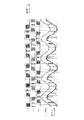
図4は、2相変調時における割り込み処理の実行時間イメージを、PWMキャリア波形と共に示すものである。エアコンにおいては、1つの制御回路(マイコン)により、圧縮機2に並行して、室外機に対応する熱交換器9のファン11を駆動するモータも制御する(室内機に対応する熱交換器7のファン10を駆動するモータは、別の制御回路やドライバICなどにより制御される)。
FIG. 4 shows an image of execution time of interrupt processing during two-phase modulation together with a PWM carrier waveform. In the air conditioner, the motor that drives the
そこで、図4では、(a)に図3に示す圧縮機2のモータ制御に関する処理時間(1)〜(4)を、(b)に上記ファン11のモータ(ファンモータ)制御に関する処理時間(5)を示している。すなわち、三角波振幅のボトムでPWM割り込みが発生すると、図3に示す処理を実行した後に、ファンモータについてもモータ電流を検出してベクトル制御を行う。図中に丸数字で示す処理(1)〜(4)については、処理(1)及び(3)はステップS2〜S8に対応し、処理(2),(4)はそれぞれステップS9,S10に対応している。この場合、ファンモータの制御(5)は、処理(4)を実行した後に行われる。
Therefore, in FIG. 4, (a) shows processing times (1) to (4) related to motor control of the
図5は、各相PWMデューティパルスの出力位相を示したもので、前述したように特許文献1に開示されている方式を用いる。すなわち、3相のうち第1相は、三角波振幅のボトムを基準として遅れ側,進み側の双方向にデューティを増減させる。また、第2相については、前記ボトムを基準として例えば進み位相側にデューティを増減させ、第3相については、前記ボトムを基準として遅れ位相側にデューティを増減させる。この例では、第1,第2,第3相がそれぞれU,V,W相となっているが、勿論これらの対応は任意である。三角波振幅のピークで割り込みが発生するとキャリアカウンタはダウンカウント中であるから、D_Pwm_set_2()により、今回のキャリア周期前半分のデューティパルスを出力する。尚、U,V,W各相のデューティ値は、ステップS11で演算されたデューティ値(後述するU0,V0,W0)を2倍したものである。
FIG. 5 shows the output phase of each phase PWM duty pulse. As described above, the method disclosed in
U相については、デューティの1/2のパルスが、ピークでの割り込みが発生した後のタイミングからボトムまでの期間に出力される。V相については、デューティが50%未満であれば、そのパルスは、U相と同様にピークでの割り込みが発生した後のタイミングからボトムまでの期間に出力される。また、W相については、デューティが50%を超えると、その超えた分のパルスは、ピークでの割り込みが発生したタイミングからボトムに達するまでの期間に出力される。したがって、D_Pwm_set_2()により出力されるのはこれらのパルスとなる。 For the U phase, a pulse with a duty of 1/2 is output in the period from the timing after the interruption at the peak to the bottom. For the V phase, if the duty is less than 50%, the pulse is output in the period from the timing after the interruption at the peak to the bottom as in the U phase. For the W phase, when the duty exceeds 50%, the excess pulses are output during the period from when the interrupt at the peak occurs until the bottom is reached. Therefore, it is these pulses that are output by D_Pwm_set_2 ().
一方、三角波振幅のボトムで割り込みが発生するとキャリアカウンタはアップカウント中であるから、D_Pwm_set_1()により、今回のキャリア周期後半分のデューティパルスを出力する。U相については、前半と同様にデューティの1/2のパルスが、ボトムでの割り込みが発生した後のタイミングからピークまでの期間に出力される。V相については、デューティが50%を超えると、その超えた分のパルスは、ボトムでの割り込みが発生したタイミングからピークに達するまでの期間に出力される。また、W相については、デューティが50%未満であれば、そのパルスは、U相と同様にボトムでの割り込みが発生した後のタイミングからピークまでの期間に出力される。したがって、D_Pwm_set_1()により出力されるのはこれらのパルスとなる。 On the other hand, when an interrupt occurs at the bottom of the triangular wave amplitude, the carrier counter is counting up, so a D_Pwm_set_1 () outputs a duty pulse for the latter half of the current carrier cycle. As for the U phase, as in the first half, a pulse having a duty of 1/2 is output in the period from the timing to the peak after the interruption at the bottom occurs. For the V phase, when the duty exceeds 50%, the excess pulses are output during the period from the timing when the interruption at the bottom occurs until the peak is reached. For the W phase, if the duty is less than 50%, the pulse is output in the period from the timing to the peak after the bottom interruption occurs, as in the U phase. Therefore, it is these pulses that are output by D_Pwm_set_1 ().
尚、図5は3相のデューティパルスを示しているが、実際の駆動形式は2相変調であるため、これらのうち2相のデューティパルスだけが出力される。
次に、図6及び図7を参照して、ステップS13の処理(StartA)について説明する。この処理では、2相変調のPWM信号における各相デューティパルスの大小関係により、パターン(0)〜(11)に分別している。尚、これらのパターンは後述する処理において、変数ptnで示されている。ここでのパターン分けは、以下の条件に基づいている。
FIG. 5 shows three-phase duty pulses, but since the actual drive format is two-phase modulation, only two-phase duty pulses are output.
Next, with reference to FIGS. 6 and 7, the process (Start A) in step S13 will be described. In this processing, the patterns are classified into patterns (0) to (11) according to the magnitude relation of the respective phase duty pulses in the two-phase modulation PWM signal. These patterns are indicated by a variable ptn in the processing described later. The pattern division here is based on the following conditions.
前記電流検出部27が、電流検出可能な最小デューティを最小幅とし、最大デューティ(100%)より、前記最小幅を減じたものを最大幅としている。例えば、電流検出可能な最小時間が10μsであり、キャリア周波数が4kHzであれば、最小幅は4%,最大幅は96%となる。また、最大幅未満で且つ最小幅を超えるデューティを中間幅とすると、2相PWM信号の出力パターンを、U,V,W相のデューティの以下の組み合わせでパターン分けする。
The
(1)U相が中間幅で、V又はW相が最大幅以上の場合
(2,3)V又はW相の何れか一方が中間幅で、他方が最大幅以上の場合
(4,6)U相と、V又はW相とが何れも最大幅以上の場合
(5)V相と、W相とが何れも最大幅以上の場合
(7)U相が0以上で、V又はW相の何れかが最小幅未満の場合
(8,9)V又はW相の何れかが0以上で、他方が最小幅未満の場合
(10,11)U相が最小幅未満で、V又はW相の何れかが0以上の場合
(0):(1)〜(11)以外の場合
図6に示すステップS21〜S33では、上記の条件に従いパターン(変数ptn)(0)〜(11)を分別している。図7には、パターン(1)〜(11)に対応する2相PWM信号パターンを示す。これらのうちパターン(4)〜(11)については、出力電圧が極めて大きい過変調状態に対応する。尚、パターン(7)について示しているのは、W相のデューティが最小幅以下の場合である。
(1) When U phase is intermediate width and V or W phase is greater than maximum width (2, 3) When either V or W phase is intermediate width and the other is greater than maximum width (4, 6) When the U phase and the V or W phase are both greater than or equal to the maximum width (5) When both the V phase and the W phase are greater than or equal to the maximum width (7) The U phase is greater than or equal to 0 and the V or W phase When either is less than the minimum width (8, 9) When either V or W phase is 0 or more and the other is less than the minimum width (10, 11) The U phase is less than the minimum width and the V or W phase When any of them is 0 or more (0): Other than (1) to (11) In steps S21 to S33 shown in FIG. 6, patterns (variable ptn) (0) to (11) are classified according to the above conditions. Yes. FIG. 7 shows two-phase PWM signal patterns corresponding to the patterns (1) to (11). Among these, patterns (4) to (11) correspond to an overmodulation state in which the output voltage is extremely large. The pattern (7) is shown when the W-phase duty is less than the minimum width.
次に、図8を参照して、ステップS14の処理(StartB)について説明する。この処理では、2相変調のPWM信号における各相デューティパルスの相対的な大小関係により、セクタ(0)〜(5)に分別している。尚、これらのセクタは後述する処理において、変数sectorで示されている。ここでのセクタ分けは、以下の条件に基づいている。
(0)U相が最大で且つV相>W相
(1)U相が最大で且つV相<W相
(2)V相が最大で且つU相>W相
(3)V相が最大で且つU相<W相
(4)W相が最大で且つU相>V相
(5)W相が最大で且つU相<V相
Next, the process (Start B) in step S14 will be described with reference to FIG. In this process, the sectors are classified into sectors (0) to (5) according to the relative magnitude relationship of each phase duty pulse in the two-phase modulation PWM signal. These sectors are indicated by a variable sector in the processing described later. The sector division here is based on the following conditions.
(0) U phase is maximum and V phase> W phase (1) U phase is maximum and V phase <W phase (2) V phase is maximum and U phase> W phase (3) V phase is maximum And U phase <W phase (4) W phase is maximum and U phase> V phase (5) W phase is maximum and U phase <V phase
図8に示すステップS41〜S45では、上記の条件に従いsector(0)〜(5)を判別している。図9は、実際にPWM信号を出力した場合に応じて変化するセクタとパターンとを示している。(a)は最大デューティが最大幅の近傍である95%の場合であり、セクタは(0)〜(5)に、パターンは(0)〜(3),(8)〜(10)で変化している。(b)は最大デューティが最大幅を超えた105%(過変調状態)の場合であり、セクタは(0)〜(5)で変化するが、パターンは(0)〜(9)で変化している。すなわち、出力電圧が高くなるほど、パターン(0)〜(3)が占める時間幅が拡がり、それらのパターン(0)〜(3)が切り替わる境界で、パターン(4)〜(11)が発生する区間が増えていることが判る。 In steps S41 to S45 shown in FIG. 8, sectors (0) to (5) are determined according to the above conditions. FIG. 9 shows sectors and patterns that change according to the actual output of the PWM signal. (A) is the case where the maximum duty is 95%, which is near the maximum width, the sector changes from (0) to (5), and the pattern changes from (0) to (3), (8) to (10). doing. (B) is a case where the maximum duty exceeds 105% (overmodulation state), and the sector changes from (0) to (5), but the pattern changes from (0) to (9). ing. That is, as the output voltage becomes higher, the time width occupied by the patterns (0) to (3) is expanded, and the section in which the patterns (4) to (11) are generated at the boundary where the patterns (0) to (3) are switched. It can be seen that is increasing.
次に、図10を参照して、ステップS15の処理(StartC)について説明する。この処理では、パターンとセクタとの組み合わせに応じて、電流検出部27が、キャリア周期内でシャント抵抗24の端子電圧をA/D変換するタイミングを決定している。尚、図中のαは、上述した電流検出可能時間や電流検出精度等を考慮して設定する(例えば、デューティ5〜10%)。PWM_MAXはデューティの最大値:100%である。
Next, the process (StartC) in step S15 will be described with reference to FIG. In this process, the
また、図中のU0,V0,W0は、図11(a)に示すように、キャリア周期の中間点(ボトム)を基点として当初決定されたU,V,W相デューティの1/2に相当する時間である。そして、V0_bai,W0_baiは、図11(b)に示すように、図5に示すパターンで3相PWM信号を出力するためにV,W相のデューティパルスをシフトした際に、キャリア周期の中間点を基点として伸びるパルスの長さに相当する。そしてtimeは、U,V,W各相のA/D変換タイミングを示す変数である。 In addition, U0, V0, and W0 in the figure correspond to 1/2 of the U, V, and W-phase duties that are initially determined with the intermediate point (bottom) of the carrier cycle as the base point, as shown in FIG. 11 (a). It is time to do. As shown in FIG. 11 (b), V0_bai and W0_bai are intermediate points of the carrier cycle when the V and W phase duty pulses are shifted in order to output the three-phase PWM signal in the pattern shown in FIG. This corresponds to the length of the pulse extending from the base point. Time is a variable indicating the A / D conversion timing of each phase of U, V, and W.
ステップS53は、パターン(1)且つセクタ(2)の場合であり、A/D変換タイミングを(PWM_MAX−α)に設定している。
ステップS54は、パターン(1)且つセクタ(4)の場合であり、A/D変換タイミングを(PWM_MAX−α)に設定している。
Step S53 is the case of pattern (1) and sector (2), and the A / D conversion timing is set to (PWM_MAX-α).
Step S54 is for pattern (1) and sector (4), and the A / D conversion timing is set to (PWM_MAX-α).
ステップS58は、パターン(3)且つセクタ(3)の場合で、且つV0_baiが(PWM_MAX×2)を超える過変調の場合であり(S57:YES)、A/D変換タイミングをαに設定している。また、ステップS59は、ステップS57で「NO」の場合であり、A/D変換タイミングを(PWM_MAX×2−V0_bai+α)に設定している。 Step S58 is the case of pattern (3) and sector (3) and overmodulation exceeding V0_bai (PWM_MAX × 2) (S57: YES), and the A / D conversion timing is set to α. Yes. Step S59 is a case of “NO” in Step S57, and the A / D conversion timing is set to (PWM_MAX × 2−V0_bai + α).
ステップS62は、パターン(2)且つセクタ(5)の場合で、且つW0_baiが(PWM_MAX×2)を超える過変調の場合であり(S61:YES)、A/D変換タイミングをαに設定している。また、ステップS63は、ステップS61で「NO」の場合であり、A/D変換タイミングを(PWM_MAX×2−W0_bai+α)に設定している。 Step S62 is a case of pattern (2) and sector (5), and a case of overmodulation in which W0_bai exceeds (PWM_MAX × 2) (S61: YES), and the A / D conversion timing is set to α. Yes. Step S63 is a case of “NO” in Step S61, and the A / D conversion timing is set to (PWM_MAX × 2−W0_bai + α).
次に、図12及び図13を参照して、ステップS16の処理(StartD)について説明する。この処理では、パターンとセクタとの組み合わせに応じて、電流検出部27が、キャリア周期内でA/D変換するタイミングを、キャリア周期の冒頭(ピーク)から1/2期間(ボトム)までのダウンカウント期間と、1/2期間からキャリア周期の終わりまでのアップカウント期間とにおいて、それぞれ何れのタイミングで行うかを決定している。前者が第1検出タイミング,後者が第2検出タイミングとなる。
尚、StartCのフローと、StartDのフローとでは、パターン及びセクタの組み合わせによる場合分けが一致している。したがって、それぞれのタイミングを設定する変数timeは、StartCにおける同じ組み合わせに対応するものを使用する。
Next, with reference to FIG. 12 and FIG. 13, the process (Start D) in step S16 will be described. In this processing, the timing at which the
Note that the start C flow and the Start D flow match the case classification according to the combination of the pattern and the sector. Therefore, the variable time for setting each timing is the one corresponding to the same combination in StartC.
パターン(0)の場合は(S71:YES)、図7に示すパターン(1)〜(11)以外の場合であり、2相の電流をそれぞれ固定したタイミングで検出可能である。したがって、ダウンカウント/アップカウントのADタイミングを、それぞれαに設定する(S72)。すなわち、キャリア周期の冒頭から残カウント値がαに達したタイミングと、キャリア周期の1/2から時間αが経過したタイミングとでA/D変換を行う。 In the case of pattern (0) (S71: YES), it is a case other than patterns (1) to (11) shown in FIG. 7, and it is possible to detect two-phase currents at fixed timings. Therefore, the down timing / up count AD timing is set to α (S72). That is, A / D conversion is performed at the timing when the remaining count value reaches α from the beginning of the carrier cycle and at the timing when time α passes from ½ of the carrier cycle.
パターン(1)で且つセクタ(2)の場合は(S74:YES)、A/D変換タイミングをアップカウント期間でtime、すなわちステップS53で決定された(PWM_MAX−α)に設定する。また、ダウンカウント期間はαに設定する(S75)。 In the case of pattern (1) and sector (2) (S74: YES) , the A / D conversion timing is set to time in the up-count period, that is, (PWM_MAX-α) determined in step S53. Further, the down-count period is set to α (S75).
パターン(1)で且つセクタ(4)の場合は(S76:YES)、アップカウント期間αに設定し、ダウンカウント期間をtime、すなわち、ステップS54で決定された(PWM_MAX−α)に設定する(S77)。また、パターン(1)で且つセクタ(2〜4)以外の場合は(S76:NO)、アップカウント期間,ダウンカウント期間をそれぞれαに設定する(S78)。 In the case of the pattern (1) and the sector (4) (S76: YES), the up-count period α is set, and the down-count period is set to time, that is, (PWM_MAX−α) determined in step S54 ( S77). If the pattern is other than the sector (2-4) (S76: NO), the up-count period and the down-count period are set to α (S78).
パターン(3)で且つセクタ(3)の場合は(S80:YES)、アップカウント期間をtime、すなわちステップS58で決定されたα,若しくはステップS59で決定された(PWM_MAX×2−V0_bai+α)に設定する。一方、ダウンカウント期間はαに設定する(S81)。 In the case of pattern (3) and sector (3) (S80: YES), the up-count period is set to time, that is, α determined in step S58, or (PWM_MAX × 2−V0_bai + α) determined in step S59. To do. On the other hand, the down-count period is set to α (S81).
パターン(3)で且つセクタ(5)の場合は(S82:YES)、アップカウント期間のタイミングをαに設定する。また、ダウンカウント期間のタイミングを、timeに、すなわちステップS60で決定された(PWM_MAX−α)に設定する(S83)。また、パターン(3)で且つセクタ(3,5)以外の場合は(S82:NO)、アップカウント期間,ダウンカウント期間をそれぞれαに設定する(S84)。 In the case of pattern (3) and sector (5) (S82: YES), the timing of the upcount period is set to α. Further, the timing of the downcount period is set to time, that is, (PWM_MAX−α) determined in step S60 (S83). If the pattern is (3) and other than sectors (3, 5) (S82: NO), the up-count period and the down-count period are set to α (S84).
図13において、パターン(2)で且つセクタ(5)の場合は(S86:YES)、アップカウント期間のタイミングをαに設定し、ダウンカウント期間のタイミングをtimeに、すなわちステップS62で決定されたα,若しくはステップS63で決定された(PWM_MAX×2−W0_bai+α)に設定する(S87)。 In FIG. 13, in the case of pattern (2) and sector (5) (S86: YES), the timing of the up-count period is set to α, and the timing of the down-count period is determined to time, that is, determined in step S62. α or (PWM_MAX × 2−W0_bai + α) determined in step S63 is set (S87).
また、パターン(2)でなければ(S85:NO)、更にパターン(10),(11)かを判断する(S85a,85c)。パターン(10)であれば(S85a:YES)、アップカウント期間のタイミングをαに,ダウンカウント期間のタイミングをα×2に設定する(S85b)。パターン(11)であれば(S85c:YES)、アップカウント期間のタイミングをα×2に,ダウンカウント期間のタイミングをαに設定する(S85d)。そして、パターン(2)で且つセクタ(5)でなければ(S86:NO)、又はパターン(11)でなければ(S85c:NO)、アップカウント期間,ダウンカウント期間のタイミングをそれぞれαに設定する(S88)。 If it is not the pattern (2) (S85: NO), it is further determined whether the pattern is (10), (11) (S85a, 85c). If it is pattern (10) (S85a: YES), the timing of the up-count period is set to α, and the timing of the down-count period is set to α × 2 (S85b). If it is the pattern (11) (S85c: YES), the timing of the up count period is set to α × 2, and the timing of the down count period is set to α (S85d). If it is not the pattern (2) and the sector (5) (S86: NO), or if it is not the pattern (11) (S85c: NO), the timing of the up-count period and the down-count period is set to α, respectively. (S88).
次に、図14及び図15を参照して、ステップS17の処理(StartE)について説明する。この処理では、第2相(V)と第3相(W)との何れか一方について、デューティパルスの増減方向を変更するために使用する変数shiftを「0〜2」の何れかに設定する。先ず、V相のデューティが最大幅以上で且つ100%未満であれば(S91:YES)、W0_baiが、PWM_MAX(図中はMAX)×2よりV0_baiを減じた差に最小幅を加算した値よりも小さく、且つW0_baiが100%未満(=W相デューティ<50%)であるか否かを判断する(S92)。この条件が成立すると(YES)変数shiftを「1」に設定し(S93)、成立しなければ(NO)変数shiftを「0」に設定する(S94)。 Next, with reference to FIG. 14 and FIG. 15, the process (StartE) in step S17 will be described. In this process, the variable shift used to change the increasing / decreasing direction of the duty pulse is set to any one of “0 to 2” for either the second phase (V) or the third phase (W). . First, if the V-phase duty is greater than or equal to the maximum width and less than 100% (S91: YES), W0_bai is obtained by adding the minimum width to the difference obtained by subtracting V0_bai from PWM_MAX (MAX in the figure) × 2. And W0_bai is less than 100% (= W-phase duty <50%) is determined (S92). If this condition is satisfied (YES), the variable shift is set to “1” (S93), and if not satisfied (NO), the variable shift is set to “0” (S94).
一方、ステップS91で「NO」と判断した場合で、W相のデューティが最大幅以上で且つ100%未満であれば(S95:YES)、V0_baiが、PWM_MAX×2よりW0_baiを減じた差に最小幅を加算した値よりも小さく、且つV0_baiが100%未満(=V相デューティ<50%)であるか否かを判断する(S96)。この条件が成立すると(YES)変数shiftを「2」に設定し(S97)、成立しなければ(NO)、変数shiftを「0」に設定する(S98)。 On the other hand, if “NO” is determined in step S91 and the W-phase duty is greater than or equal to the maximum width and less than 100% (S95: YES), V0_bai is the maximum difference obtained by subtracting W0_bai from PWM_MAX × 2. It is determined whether or not V0_bai is less than 100% (= V-phase duty <50%), which is smaller than the value obtained by adding the small width (S96). If this condition is satisfied (YES), the variable shift is set to “2” (S97). If not satisfied (NO), the variable shift is set to “0” (S98).
図15(a),(b)は、パターン(3)の場合を例示している。パターン(3)は、V相のデューティが最大幅以上であり、且つW相のデューティが最小幅以上の場合である。図15(a)に示すように、固定の第1検出タイミングではV相電流が検出され、可変の第2検出タイミングでは負のU相電流が検出される。しかし、この状態からV,W相デューティの少なくとも一方が減少する方向に変化することで、第2検出タイミングにおいてV,W相デューティパルスが重複する期間がなくなると、負のU相電流が検出されず、第1検出タイミングと同じV相電流若しくはW相電流が検出されてしまう。 FIGS. 15A and 15B illustrate the case of the pattern (3). Pattern (3) is a case where the V-phase duty is greater than or equal to the maximum width and the W-phase duty is greater than or equal to the minimum width. As shown in FIG. 15A, the V-phase current is detected at the fixed first detection timing, and the negative U-phase current is detected at the variable second detection timing. However, when at least one of the V and W phase duty decreases from this state, and when there is no period in which the V and W phase duty pulses overlap at the second detection timing, a negative U phase current is detected. Therefore, the same V-phase current or W-phase current as the first detection timing is detected.
そこで、図15(b)に示すように、W相デューティを増加させる方向をV相デューティと同じ方向に変更する。これにより、固定の第1検出タイミングでは負のU相電流が検出され、可変の第2検出タイミングではV相電流が検出されるように入れ替わる。したがって、V相デューティが減少すれば、それに合わせて第2検出タイミングを図中右方向にシフトさせて対応すれば良い。また、W相デューティが減少しても、最小幅以上であれば、固定の第1検出タイミングで検出が可能である。 Therefore, as shown in FIG. 15B, the direction in which the W-phase duty is increased is changed to the same direction as the V-phase duty. As a result, the negative U-phase current is detected at the fixed first detection timing, and the V-phase current is detected at the variable second detection timing. Therefore, if the V-phase duty is reduced, the second detection timing may be shifted in the right direction in the drawing to cope with it. Further, even if the W-phase duty is reduced, if the width is equal to or greater than the minimum width, detection is possible at the fixed first detection timing.
また、図15(c)は、パターン(3)の場合で変数shiftを「1」に設定するケースである。図中丸数字の「1」を付した矢印は、ステップS92の条件判定における「MAX×2(PWM_MAX×2)よりV0_baiを減じた差」に最小幅を加算した値を示しており、丸数字の「2」を付した矢印はW0_baiを示している。ここで変数shiftを「1」に設定するのは、アップカウント区間のV相デューティの左端(可変端)側とW相デューティの右端(可変端)側とが重複するケースである。 FIG. 15C shows a case where the variable shift is set to “1” in the case of the pattern (3). The arrow with the circled number “1” in the figure indicates the value obtained by adding the minimum width to “the difference obtained by subtracting V0_bai from MAX × 2 (PWM_MAX × 2)” in the condition determination in step S92. The arrow with “2” indicates W0_bai. Here, the variable shift is set to “1” in the case where the left end (variable end) side of the V-phase duty and the right end (variable end) side of the W-phase duty overlap in the up-count section.
また、図15(d)は、パターン(2)の場合で変数shiftを「2」に設定するケースである。図中丸数字の「3」を付した矢印は、ステップS96の条件判定における「MAX×2よりW0_baiを減じた差」に最小幅を加算した値を示しており、丸数字の「4」を付した矢印はV0_baiを示している。ここで変数shiftを「2」に設定するのは、図15(c)と同様に、ダウンカウント区間のV相デューティの左端(可変端)側とW相デューティの右端(可変端)側とが重複するケースである。 FIG. 15D shows a case where the variable shift is set to “2” in the case of the pattern (2). The arrow with the circled number “3” in the figure indicates the value obtained by adding the minimum width to “the difference obtained by subtracting W0_bai from MAX × 2” in the condition determination in step S96, and the circled number “4” is added. The indicated arrow indicates V0_bai. Here, the variable shift is set to “2” because, like FIG. 15C, the left end (variable end) side of the V-phase duty and the right end (variable end) side of the W-phase duty in the down-count section are set. This is an overlapping case.
次に、図16から図18を参照して、ステップS3の処理(StartF)について説明する。この処理では、以上までの処理で決定されたパターンとセクタとの組み合わせ,及びその組み合わせにより決定された相電流の第1,第2検出タイミングにより、キャリア周期内で2相の電流を検出(A/D変換)する。そして、検出した2相の電流から、3相の電流を求める。 Next, with reference to FIG. 16 to FIG. 18, the process (Start F) of step S3 will be described. In this process, the two-phase current is detected within the carrier period based on the combination of the pattern and sector determined in the above processes and the first and second detection timings of the phase current determined by the combination (A / D conversion). Then, a three-phase current is obtained from the detected two-phase current.
図16に示すパターン(4)〜(11)については、図7で示したように、何れか1相以上の出力電圧が極めて大きい過変調状態のケースであり、キャリア周期内で2相の出力を検出することが困難であるから、1相のみの電流を検出する。パターン(4),(7),(8),(10)であればダウンカウントタイミングで、パターン(5),(6),(9),(11)であればアップカウントタイミングで、それぞれW相(S102),U相(S104),V相(S106),U相(S108),V相(S110),W相(S112),V相(S114),W相(S116)電流を取得する。尚、U相デューティが最小幅以下となるパターン(10),(11)の場合、電流検出タイミングはα×2とする。 Patterns (4) to (11) shown in FIG. 16 are cases of an overmodulation state in which the output voltage of one or more phases is extremely large as shown in FIG. 7, and two-phase output is performed within the carrier period. Since it is difficult to detect the current, only the current of one phase is detected. The patterns (4), (7), (8), and (10) are down-count timing, and the patterns (5), (6), (9), and (11) are up-count timing, respectively. Phase (S102), U phase (S104), V phase (S106), U phase (S108), V phase (S110), W phase (S112), V phase (S114), and W phase (S116) currents are acquired. . In the case of patterns (10) and (11) in which the U-phase duty is less than the minimum width, the current detection timing is α × 2.
図17において、セクタ(0)であれば、第1検出タイミング(ダウンカウント時),第2検出タイミング(アップカウント時)によりW,U相電流を検出し、V相電流は検出した2相電流から演算により求める(S118)。尚、図17及び図18において、変数R_Iuに格納するA/D変換値(右辺)に符号−を付しているのは、A/D変換器の入力側で反転増幅を行っているためである。検出されるW相電流の符号は負であるため、R_Iwに格納する際に符号−は付さない。以下、説明上、符号−の有無については言及しない。 In FIG. 17, in the case of sector (0), the W and U phase currents are detected at the first detection timing (during down count) and the second detection timing (at the time of up count), and the V phase current is the detected two phase current. Is obtained by calculation (S118). In FIG. 17 and FIG. 18, the reason that the A / D conversion value (right side) stored in the variable R_Iu is attached with a sign-is because inverting amplification is performed on the input side of the A / D converter. is there. Since the sign of the detected W-phase current is negative, the sign-is not added when storing in R_Iw. Hereinafter, in the description, the presence or absence of the sign-is not mentioned.
セクタ(1)であれば、第1,第2検出タイミングによりU,V相電流を検出し、W相電流は演算により求める(S120)。セクタ(2)の場合は、パターン(1)か否かを判断し(ステップS122)、パターン(1)であれば(YES)第1,第2検出タイミングによりW,V相電流を検出する(S123)。一方、パターン(1)でなければ(NO)第1,第2検出タイミングによりW,U相電流を検出し、V相電流は演算により求める(S124)。 If it is sector (1), the U and V phase currents are detected at the first and second detection timings, and the W phase current is obtained by calculation (S120). In the case of sector (2), it is determined whether or not it is pattern (1) (step S122). If it is pattern (1) (YES), W and V phase currents are detected at the first and second detection timings ( S123). On the other hand, if it is not the pattern (1) (NO), the W and U phase currents are detected at the first and second detection timings, and the V phase current is obtained by calculation (S124).
セクタ(3)であれば(S125:YES)、変数shiftが「1」か否かを判断し(S126)、「1」であれば(YES)第1,第2検出タイミングによりU,V相電流を検出する(S127)。一方、「1」でなければ(NO)パターン(1)か否かを判断し(S128)、パターン(1)であれば(YES)第1,第2検出タイミングによりV,U相電流を検出する(S129)。一方、パターン(1)でなければ(NO)第1,第2検出タイミングによりV,W相電流を検出する(S130)。 If it is the sector (3) (S125: YES), it is determined whether or not the variable shift is “1” (S126). If it is “1” (YES), the U and V phases are detected at the first and second detection timings. The current is detected (S127). On the other hand, if it is not “1” (NO), it is determined whether or not the pattern is (1) (S128). If it is pattern (1) (YES), the V and U phase currents are detected at the first and second detection timings. (S129). On the other hand, if the pattern is not (1) (NO), the V and W phase currents are detected at the first and second detection timings (S130).
一方、ステップS125においてセクタ(3)でなければ(NO)、図18に示すように、更にセクタ(4)か否か(S131)、パターン(1)か否か(S132)が判断される。セクタ(4)で且つパターン(1)の場合(S132:YES)、第1,第2検出タイミングによりW,V相電流を検出する(S133)。また、パターン(1)でなければ(S132:NO)、第1,第2検出タイミングによりU,V相電流を検出する(S134)。 On the other hand, if it is not sector (3) in step S125 (NO), as shown in FIG. 18, it is further determined whether it is sector (4) (S131) or pattern (1) (S132). In the case of sector (4) and pattern (1) (S132: YES), W and V phase currents are detected at the first and second detection timings (S133). If the pattern is not the pattern (1) (S132: NO), the U and V phase currents are detected at the first and second detection timings (S134).
また、ステップS131でセクタ(4)でなければ(NO)セクタ(5)のケースであり、変数shiftが「2」か否か(S135)が判断される。変数shiftが「2」の場合(YES)、第1,第2検出タイミングによりW,U相電流を検出する(S136)。また、ステップS135で「NO」と判断すると、パターン(2)か否かが判断され(S137)、パターン(2)であれば(YES)、第1,第2検出タイミングによりU,W相電流を検出する(S138)。パターン(2)でなければ(S137:NO)、第1,第2検出タイミングによりV,W相電流を検出する(S141)。 In step S131, if the sector is not sector (4) (NO), it is the case of sector (5), and it is determined whether or not the variable shift is “2” (S135). When the variable shift is “2” (YES), the W and U phase currents are detected at the first and second detection timings (S136). If “NO” is determined in the step S135, it is determined whether or not the pattern is the pattern (2) (S137). If the pattern is the pattern (2) (YES), the U and W phase currents are determined at the first and second detection timings. Is detected (S138). If it is not the pattern (2) (S137: NO), the V and W phase currents are detected at the first and second detection timings (S141).
以上に述べたパターンとセクタとの組み合わせに応じて、最終的に第1,第2電流検出タイミングがどのように決まるかを、図19から図23を参照して説明する。図19はパターン(0)の場合であり、セクタは(0〜5)の全てを取り得る。(b)は実際の2相変調のPWM信号波形と、対応するパターンとセクタとの組み合わせを示す。セクタに応じて検出対象となる相は異なるが、第1,第2電流検出タイミングは、何れも固定タイミング(ダウンカウント,アップカウントの何れもα)となる。 How the first and second current detection timings are finally determined according to the combination of the pattern and the sector described above will be described with reference to FIGS. FIG. 19 shows the case of pattern (0), and the sector can take all of (0 to 5). (B) shows a combination of an actual two-phase modulation PWM signal waveform and a corresponding pattern and sector. Although the phases to be detected are different depending on the sector, the first and second current detection timings are both fixed timings (both down count and up count are α).
図20はパターン(1)の場合であり、セクタは(2,4)となる。これらの場合も、第1,第2電流検出タイミングは何れも固定タイミングである。但し、一方はα,他方は(PMW_MAX−α)となる。 FIG. 20 shows the case of pattern (1), and the sector is (2, 4). In these cases, the first and second current detection timings are both fixed timings. However, one is α and the other is (PMW_MAX−α).
図21はパターン(2)の場合であり、セクタは(5)だけとなるが、W0_baiがPWM_MAX×2を超えるか否か、シフト(2)か否かに応じて3つのケースに分かれる。W0_baiがPWM_MAX×2を超える場合、第1,第2電流検出タイミングは何れも固定となる。W0_baiがPWM_MAX×2を超えない場合、第1電流検出タイミングは可変となり、しかも、シフト(2)の場合は、V相のデューティ増減方向をW相と同じにする。その結果、検出対象となる相は、(U,W)→(W,U)に変更される。 FIG. 21 shows the case of pattern (2). The sector is only (5), but there are three cases depending on whether W0_bai exceeds PWM_MAX × 2 or shift (2). When W0_bai exceeds PWM_MAX × 2, the first and second current detection timings are both fixed. When W0_bai does not exceed PWM_MAX × 2, the first current detection timing is variable, and in the case of shift (2), the V phase duty increase / decrease direction is made the same as the W phase. As a result, the phase to be detected is changed from (U, W) to (W, U).
図22はパターン(3)の場合であり、セクタは(3)のみとなるが、更にV0_baiがPWM_MAX×2を超えるか否か、シフト(1)か否かに応じて3つのケースに分かれる。V0_baiがPWM_MAX×2を超える場合、第1,第2電流検出タイミングは何れも固定となる。V0_baiがPWM_MAX×2を超えない場合、第2電流検出タイミングは可変となり、しかも、シフト(1)の場合は、W相のデューティ増減方向をV相と同じにする。その結果、検出対象となる相は、(V,U)→(U,V)に変更される。図23はパターン(4)〜(11)の場合で、図16に対応している。 FIG. 22 shows the case of pattern (3). The sector is only (3), but it is further divided into three cases depending on whether V0_bai exceeds PWM_MAX × 2 or shift (1). When V0_bai exceeds PWM_MAX × 2, the first and second current detection timings are both fixed. When V0_bai does not exceed PWM_MAX × 2, the second current detection timing is variable, and in the case of shift (1), the W phase duty increase / decrease direction is made the same as the V phase. As a result, the phase to be detected is changed from (V, U) to (U, V). FIG. 23 shows patterns (4) to (11) and corresponds to FIG.
図24は、パターン(2)又は(3)の場合における検出タイミングの特徴的な変化の一例を示す。(a)に示すように、V,W相デューティパルスが互いに重複する期間が無い状態で出力されており、第1,第2検出タイミングにおいて、それぞれV,W相電流を検出している状態から、W相デューティが96%を超えることでキャリア周期の前半でV,W相デューティパルスが互いに重複する期間が発生する。この場合、第1検出タイミングで検出される電流の相はU相(−)に変更される。
この状態から、V又はW相デューティが減少すると、第1検出タイミングが固定のままではV,W相デューティパルスが互いに重複する期間より外れて、U相電流が検出できなくなる可能性がある。そこで、第1検出タイミングを可変にして、V,W相デューティパルスの重複期間内で継続してU相電流を検出する。
FIG. 24 shows an example of a characteristic change in detection timing in the case of pattern (2) or (3). As shown in (a), the V and W phase duty pulses are output without a period in which they overlap each other, and the V and W phase currents are detected at the first and second detection timings, respectively. When the W-phase duty exceeds 96%, a period in which the V and W-phase duty pulses overlap each other occurs in the first half of the carrier cycle. In this case, the phase of the current detected at the first detection timing is changed to the U phase (−).
If the V or W phase duty is reduced from this state, there is a possibility that the U phase current cannot be detected because the V and W phase duty pulses deviate from each other when the first detection timing remains fixed. Therefore, the first detection timing is made variable, and the U-phase current is detected continuously within the overlapping period of the V and W-phase duty pulses.
図24(b)は、V相デューティが96%を超えることで、キャリア周期の後半でV,W相デューティパルスが互いに重複する期間が発生したケースである。この場合、第2検出タイミングで検出される電流の相はU相(−)に変更される。この状態から、V又はW相デューティが減少すると、第2検出タイミングが固定のままではV,W相デューティパルスが互いに重複する期間より外れて、U相電流が検出できなくなる可能性がある。そこで、第2検出タイミングを可変にして、V,W相デューティパルスの重複期間内で継続してU相電流を検出する。 FIG. 24B shows a case where a period in which the V and W phase duty pulses overlap each other in the latter half of the carrier cycle due to the V phase duty exceeding 96%. In this case, the phase of the current detected at the second detection timing is changed to the U phase (−). If the V or W phase duty is reduced from this state, there is a possibility that the U phase current cannot be detected because the V and W phase duty pulses deviate from each other when the second detection timing remains fixed. Therefore, the second detection timing is made variable, and the U-phase current is detected continuously within the overlapping period of the V and W-phase duty pulses.
図25は、パターン(1)の場合における検出タイミングの特徴的な変化の一例を示す。(a)に示すように、U,V相デューティパルスが互いに重複する期間がキャリア周期の前半のみで生じており、第1,第2検出タイミングでそれぞれW(−),U相電流を検出している。この状態から、V相デューティが96%を超えることでキャリア周期の後半でも重複する期間が発生する。この場合、第2検出タイミングで検出される電流もW相(−)となってしまう。したがって、第2検出タイミングを変更して、V相デューティパルスのみが発生している期間でV相電流を検出する。この状態を維持するためには、第2検出タイミングを変更したタイミングで固定する(但し、V相デューティの変化によっては可変にしても良い)。 FIG. 25 shows an example of a characteristic change in detection timing in the case of pattern (1). As shown in (a), the period in which the U and V phase duty pulses overlap each other occurs only in the first half of the carrier cycle, and W (−) and U phase currents are detected at the first and second detection timings, respectively. ing. From this state, when the V-phase duty exceeds 96%, an overlapping period occurs even in the second half of the carrier cycle. In this case, the current detected at the second detection timing is also the W phase (−). Therefore, the second detection timing is changed, and the V-phase current is detected in a period in which only the V-phase duty pulse is generated. In order to maintain this state, the second detection timing is fixed at the changed timing (however, it may be variable depending on the change in the V-phase duty).
図25(b)は、W相デューティが96%を超えることで、キャリア周期の前半でU,W相デューティパルスが互いに重複する期間が発生したケースである。この場合、第1検出タイミングを変更して、W相デューティパルスのみが発生している期間でW相電流を検出する。この状態を維持するためには、第1検出タイミングを変更したタイミングで固定する(但し、W相デューティの変化によっては可変にしても良い)。 FIG. 25B shows a case where a period in which the U and W phase duty pulses overlap each other occurs in the first half of the carrier cycle because the W phase duty exceeds 96%. In this case, the first detection timing is changed, and the W-phase current is detected during a period in which only the W-phase duty pulse is generated. In order to maintain this state, the first detection timing is fixed at the changed timing (however, it may be made variable depending on the change in the W-phase duty).
図26は、変調率がほぼ1.0の場合に、(a)本実施形態の方式で検出されるモータ電流の波形と、(b)特許文献1の方式で検出されるモータ電流の波形とを示している。この図から明らかなように、本実施形態の方が電流検出率が向上する結果、電流波形はより歪が少なく正弦波に近いものとなっている。
FIG. 26 shows (a) the motor current waveform detected by the method of the present embodiment and (b) the motor current waveform detected by the method of
以上のように本実施形態によれば、電流検出部27は、インバータ回路23の直流側に接続されるシャント抵抗24が電流値に対応して発生した信号とPWM信号パターンとに基づいてモータ4の相電流Iu,Iv,Iwを検出し、ベクトル制御部30は相電流に基づいてロータ位置θを決定し、PWM信号生成部32と共に、ロータ位置θに追従するように3相のうち何れか2相のPWM信号パターンを生成する。このとき、PWM信号生成部32は、3相PWM信号パターンのU相は、キャリア周期のボトムを基準として遅れ側,進み側の双方向にデューティを増減させ、V相は、前記ボトムを基準として遅れ側,進み側の一方向に、W相は前記方向とは逆方向にデューティを増減させる。
As described above, according to the present embodiment, the
そして、電流検出タイミング調整部34は、キャリア周期内において、2相変調における一方の相については固定されたタイミングで電流を検出し、他方の相については、固定されたタイミングで電流を検出するか、又は前記インバータ回路23に対する出力電圧の大きさに応じた可変のタイミングで電流を検出可能となるように検出タイミングを調整する。したがって、出力電圧が高く、過変調状態となる領域においても電流検出率を向上させることができ、スイッチング損失を抑制しつつ制御精度の向上を図ることができる。
Then, the current detection
また、電流検出タイミング調整部34は、前記他方の相についての電流検出を、予め定めた固定タイミングとするか、固定タイミングより変化させたタイミングとするかを、2相のPWM信号パターンに応じて決定する。具体的には、電流検出部27が、電流検出可能な最小デューティを最小幅とし、その最小幅に基づいて最大幅,中間幅を定め、2相PWM信号の出力パターンを、前記各幅の何れかに該当する3相デューティの組み合わせでパターン(0〜11)に場合分けし、3相デューティの大小関係によりセクタ(0〜5)に場合分けする。そして、パターン(0〜11)とセクタ(0〜5)との組み合わせに応じて、前記他方の相についての電流検出を、予め定めた固定タイミングとするか、変化させたタイミングとするかを決定する。
The current detection
これにより、2相変調におけるPWM信号の各組合せに応じて、電流検出タイミングの他方を可変にするか否かを妥当に判定できる。また、出力電圧が極めて高い過変調状態において、実質的に1相の電流しか検出できない状態についても確実に見極めて、電流検出を行い、極力モータ制御に利用することができる。 This makes it possible to appropriately determine whether or not to make the other one of the current detection timings variable in accordance with each combination of PWM signals in two-phase modulation. In addition, in an overmodulation state where the output voltage is extremely high, it is possible to reliably detect a state in which only one-phase current can be detected, to detect the current and use it for motor control as much as possible.
電流検出タイミング調整部34は、他方の相についての電流検出を予め定めた固定タイミングとしており、キャリア周期内にデューティパルスが出力されている2相がV,W相であって、双方の固定タイミングで検出される2相の電流がV,W相である状態から、これら2相のデューティパルスの出力タイミングに重なる期間が発生すると、検出対象とする相の一方をU相に変更する。したがって、確実に2相の電流を検出できる。
The current detection
また、電流検出タイミング調整部34は、検出対象とする相の一方をU相に変更した後に、V又はW相のデューティパルスが互いに重なる期間が変動すると、U相の検出が可能となる範囲で、電流検出タイミングを変更する。これにより、変更した検出対象相を維持するようにして、再度変更を重ねることを極力防止できる。
In addition, the current detection
また、電流検出タイミング調整部34は、キャリア周期内にデューティパルスが出力されている2相が、U相とV又はW相とであって、双方の固定タイミングで検出される2相の電流がU相とW又はV相とである状態から、U相の電流が検出できない状態になると、他方の相についての電流検出を可変タイミングとして、検出対象とする相の一方をU相からV又はW相に変更する。したがって、この場合も確実に2相の電流を検出できる。そして、電流検出タイミング調整部34は、前記他方の相についての電流検出タイミングを一度変更した後に、その変更後のタイミングを固定してV又はW相の電流を検出する。この場合も、変更後の検出対象相を維持して再度変更を重ねることを極力防止できる。
Further, the current detection
更に、電流検出タイミング調整部34は、キャリア周期内にデューティパルスが出力されている2相がV及びW相であり、これらの一方のデューティが減少することで2相の電流が検出できなくなると、デューティが小さい方の相のデューティ増減方向を、他の相と同じ方向に変更する。これにより、2相のデューティパルスが互いに重なる期間が発生するようになり、2相の電流が検出可能となる。
Furthermore, the current detection
更に、圧縮機2と、室外側熱交換器9と、減圧装置8と、室内側熱交換器7とを備えるヒートポンプシステム1を備える空気調和機Eについて、圧縮機2を構成するモータ4を制御対象とするので、ヒートポンプシステム1及び空気調和機Eの運転効率を向上させることができる。
Furthermore, the
(第2実施形態)
図27から図33は第2実施形態であり、第1実施形態と同一部分には同一符号を付して説明を省略し、以下異なる部分について説明する。第1実施形態では、例えば図22に示したように、パターン(3)で且つセクタ(3)の組み合わせで変数shiftが「1」になると、W相のデューティ増減方向をV相と同じ方向に変更した。第2実施形態では、同じケースについて異なる対応を行う。
(Second Embodiment)
FIG. 27 to FIG. 33 show the second embodiment. The same parts as those of the first embodiment are denoted by the same reference numerals, description thereof is omitted, and different parts will be described below. In the first embodiment, for example, as shown in FIG. 22, when the variable shift is “1” in the combination of the pattern (3) and the sector (3), the W phase duty increase / decrease direction is set to the same direction as the V phase. changed. In the second embodiment, different actions are taken for the same case.
すなわち、図27(a)に示すように、U相のデューティパルスも出力させる。そして、前記デューティパルスの分だけV,W相のデューティパルスを増加させて、一時的に3相変調状態にする。この場合、U,V,W間の相間電圧に変化はないので、出力電圧自体は変化しない。更にこの時、第1電流検出タイミングについても可変とする。これにより、第2検出タイミングの検出対象となる相を変更させることなく電流検出率が向上する。 That is, as shown in FIG. 27A, a U-phase duty pulse is also output. Then, the V-phase and W-phase duty pulses are increased by the amount of the duty pulse to temporarily enter a three-phase modulation state. In this case, since the interphase voltage between U, V, and W does not change, the output voltage itself does not change. At this time, the first current detection timing is also variable. As a result, the current detection rate is improved without changing the phase to be detected at the second detection timing.
また、図27(b)は、第1実施形態では図20に示した、パターン(2)で且つセクタ(5)の組み合わせで変数shiftが「2」になるケースに対応する。この場合も同様に、U相のデューティパルスも出力させ、前記デューティパルスの分だけV,W相のデューティパルスを増加させて一時的に3相変調状態にする。これらの処理パターンを含む一覧を、図28及び図29(第1実施形態の図21及び図22相当図)に示している。 FIG. 27B corresponds to the case where the variable shift is “2” in the combination of the pattern (2) and the sector (5) shown in FIG. 20 in the first embodiment. In this case as well, a U-phase duty pulse is also output, and the V and W-phase duty pulses are increased by the amount corresponding to the duty pulse to temporarily enter a three-phase modulation state. A list including these processing patterns is shown in FIGS. 28 and 29 (corresponding to FIGS. 21 and 22 in the first embodiment).
図30から図31は、第1実施形態の図12及び図13に相当するStartDのフローチャートである。ただし、図30は、図12におけるステップS71〜S79のみを示しており、ステップS79で「YES」と判断すると、図32に示す処理に移行する。図31では、パターン(2)で且つセクタ(5)の場合に(S86:YES)変数shiftが「0」か否かを判断し(S151)、変数shiftが「0」であれば(YES)ステップS87を実行する。一方、変数shiftが「0」でなければ(NO)、第1,第2検出タイミングを、U相デューティパルスにαを加えたものに設定する(S152)。 30 to 31 are flowcharts of StartD corresponding to FIGS. 12 and 13 of the first embodiment. However, FIG. 30 shows only steps S71 to S79 in FIG. 12. If “YES” is determined in the step S79, the process proceeds to the process shown in FIG. In FIG. 31, in the case of the pattern (2) and the sector (5) (S86: YES), it is determined whether or not the variable shift is “0” (S151), and if the variable shift is “0” (YES). Step S87 is executed. On the other hand, if the variable shift is not “0” (NO), the first and second detection timings are set to a value obtained by adding α to the U-phase duty pulse (S152).
図32では、パターン(3)で且つセクタ(3)の場合に(S80:YES)変数shiftが「0」か否かを判断し(S153)、変数shiftが「0」であれば(YES)ステップS81を実行する。一方、変数shiftが「0」でなければ(NO)、S152と同様の処理となる(S154)。また、パターン(3)で且つセクタ(5)の場合も(S82:YES)変数shiftが「0」か否かを判断し(S157)、変数shiftが「0」であれば(YES)ステップS83を実行する。一方、変数shiftが「0」でなければ(NO)、S152と同様の処理となる(S156)。また、図33は図18相当図であり、StartFの処理の一部である。 In FIG. 32, in the case of the pattern (3) and the sector (3) (S80: YES), it is determined whether or not the variable shift is “0” (S153), and if the variable shift is “0” (YES). Step S81 is executed. On the other hand, if the variable shift is not “0” (NO), the process is the same as S152 (S154). Also in the case of pattern (3) and sector (5) (S82: YES), it is determined whether or not the variable shift is “0” (S157). If the variable shift is “0” (YES), step S83. Execute. On the other hand, if the variable shift is not “0” (NO), the process is the same as S152 (S156). FIG. 33 is a view corresponding to FIG. 18 and is a part of the StartF process.
以上のように第2実施形態によれば、電流検出タイミング調整部34は、他方の相についての電流検出を可変タイミングとしており、キャリア周期内にデューティパルスが出力されている2相がV及びW相であり、これら2相のうち一方のデューティが減少することで2相の電流が検出できない状態になると、U相のデューティパルスを所定値だけ発生させると共に、V及びW相のデューティパルスを前記所定値だけ増加させる。そして、一方の相についての電流検出も可変タイミングとする。これにより、電流検出率を向上させることができる。
As described above, according to the second embodiment, the current detection
(第3実施形態)
図34から図45は第3実施形態を示すものである。第1,第2実施形態では、図34に破線で示すように、モータ4の回転数に関わらず相電流が1相分しか検出できない区間が発生する。そこで、図35に示すように、U,V,W相のPWMパルスに対し、2相の電流が検出可能となる最小幅のパルスを加えることで、第2実施形態と同様に2相変調を一時的に3相変調化する。
(Third embodiment)
34 to 45 show a third embodiment. In the first and second embodiments, as indicated by a broken line in FIG. 34, there is a section in which the phase current can be detected only for one phase regardless of the rotation speed of the
図35に示す例では、(a)2相変調の状態ではV相のデューティが小さいため、2回ともU相電流を検出することになる。(b)これに対して、所定デューティ値のW相パルスを追加すると共に、前記デューティ値をU,V相パルスにも追加することで3相変調化すると、W,V相電流(何れも負)が検出可能となる。この場合、U,V,Wの2相間の電圧(相間電圧)に変化はないのでモータ4に対する出力電圧自体は変化せず、電流検出率を向上させることができる。
In the example shown in FIG. 35, (a) in the two-phase modulation state, the V-phase duty is small, so the U-phase current is detected twice. (B) On the other hand, when a three-phase modulation is performed by adding a W-phase pulse having a predetermined duty value and also adding the duty value to the U and V-phase pulses, the W and V-phase currents (both negative) ) Can be detected. In this case, since there is no change in the voltage between U, V, and W (phase voltage), the output voltage itself to the
図36は、第1実施形態の図6に示すStartAのフローチャートを実行した後に続いて実行される処理(StartA+)である。この処理では、2相変調のPWM信号における各相デューティパルスの大小関係に応じて、変数Ptn_3phs_chで示されるパターン(0)〜(5)に分別する。ここでのパターン分けは、以下の条件に基づいている。 FIG. 36 is a process (StartA +) that is subsequently executed after executing the flowchart of StartA shown in FIG. 6 of the first embodiment. In this process, the patterns are classified into patterns (0) to (5) indicated by the variable Ptn_3phs_ch according to the magnitude relationship of the duty pulses of the respective phases in the PWM signal of the two-phase modulation. The pattern division here is based on the following conditions.
電流検出部27が電流検出可能となる最小デューティを最小幅とし、最大デューティ(100%)より前記最小幅を減じたものを最大幅としている。例えば、電流検出可能な最小時間が10μsであり、キャリア周波数が4kHzであれば、最小幅は4%,最大幅は96%となる。2相PWM信号の出力パターンを、U,V,W相のデューティの以下の組み合わせでパターン分けする。U0bai_2,V0bai_2,W0bai_2は、ステップS11で演算される2相変調時のU,V,W相のデューティ値の2倍である。
(1)W0bai_2が最大幅未満又はV0bai_2が最大幅未満 で、且つU0bai_2/2又はV0bai_2又はW0bai_2が最小幅未満で且つ0以上
(2)W0bai_2が最大幅以上又はV0bai_2が最大幅以上で、且つU0bai_2の1/2が最小幅以上で、且つV0bai_2が最小幅未満で且つ0以上
(3)W0bai_2が最大幅以上又はV0bai_2が最大幅以上で、且つU0bai_2の1/2が最小幅以上で、且つW0bai_2が最小幅未満で且つ0以上
(4)W0bai_2が最大幅以上又はV0bai_2が最大幅以上で、且つU0bai_2の1/2が最小幅未満で且つ0以上で、且つV0bai_2がW0bai_2より大きい
(5)W0bai_2が最大幅以上又はV0bai_2が最大幅以上で、且つU0bai_2の1/2が最小幅未満且つ0以上で、且つV0bai_2がW0bai_2より小さい
(0)上記以外の場合
上記の条件に従い、パターン(0)〜(5);変数Ptn_3phs_chを分別している。
The minimum duty at which the
(1) W0bai_2 is less than maximum width or V0bai_2 is less than maximum width and U0bai_2 / 2 or V0bai_2 or W0bai_2 is less than minimum width and 0 or more (2) W0bai_2 is more than maximum width or V0bai_2 is more than maximum width and
図37は、第1実施形態の図12及び図13に示すStartDのフローチャートにおいて、ステップS88の実行後に移行する処理(StartD+)であり、変数Ptn_3phs_chに応じて、アップカウント及びダウンカウント時のADタイミングを決定している。Ptn_3phs_chが(2)〜(5)の場合に、アップカウント、ダウンカウント時で電流検出タイミングをα×3としているのは(S172,S174)、1相分のPWMパルスがONしているタイミングで電流検出するためであり、倍率は他の値、例えば2倍でも良い。パターン(0),(1)の場合は、2回とも固定タイミングαとなる(S175)。 FIG. 37 is a process (StartD +) that shifts after execution of step S88 in the flowchart of StartD shown in FIGS. 12 and 13 of the first embodiment, and AD timing at the time of up-counting and down-counting according to the variable Ptn_3phs_ch Is determined. When Ptn_3phs_ch is (2) to (5), the current detection timing is set to α × 3 at the time of up-counting and down-counting (S172, S174) at the timing when the PWM pulse for one phase is ON. This is for detecting the current, and the magnification may be another value, for example, twice. In the case of patterns (0) and (1), the fixed timing α is set twice (S175).
図38は、第1実施形態の図16から図18に示すStartFのフローチャートにおいて、ステップS141の実行後に移行する処理(StartF+)であり、Ptn_3phs_chに応じて電流を検出する2相を決定する。 FIG. 38 is a process (StartF +) that shifts after the execution of step S141 in the flowchart of StartF shown in FIGS. 16 to 18 of the first embodiment, and determines two phases for detecting a current according to Ptn_3phs_ch.
図39は、ステップS11に相当するPWM出力のフローチャートである。この処理では2相変調用のデューティU02,V02,W02を決定するため、Ptn_3phs_ch=0の場合は、3相変調で計算された各デューティ値U0,V0,W0よりU,V,W相の最小デューティ値Min_Dutyを減算する(S192)。一方、Ptn_3phs_ch≠0の場合は、補正デューティ値となるDutyChang=Min_Duty−αとすることで3相変調化する(S195)。 FIG. 39 is a flowchart of PWM output corresponding to step S11. In this process, the duties U02, V02, and W02 for two-phase modulation are determined. When Ptn_3phs_ch = 0, the minimum of U, V, and W phases is calculated from the respective duty values U0, V0, and W0 calculated by three-phase modulation. The duty value Min_Duty is subtracted (S192). On the other hand, when Ptn_3phs_ch ≠ 0, three-phase modulation is performed by setting DutyChang = Min_Duty−α as a correction duty value (S195).
図40に、2相変調時のPWM出力を3相変調化したPWMパルス波形を示す。この例では、2相変調ではパルス出力が無かったU相を、パルス幅α×2で出力すると共に、V,W相パルスにもパルス幅α×2を追加することで3相変調化している。 FIG. 40 shows a PWM pulse waveform obtained by converting the PWM output during two-phase modulation into three-phase modulation. In this example, the U phase, which has no pulse output in the two-phase modulation, is output with the pulse width α × 2, and the three-phase modulation is performed by adding the pulse width α × 2 to the V and W phase pulses. .
図41は、ステップS10に相当するD_Pwm_set_1()のU相デューティ値を決定する部分のフローチャートである。第3実施形態では、2相変調時のPWM出力を3相変調化するが、図42に示すように、例えばPtn_3phs_ch=4の場合、電流検出時間が十分に確保できない場合がある。この例では、V相パルスのデューティが100%に近付く大きな値となっていることで(a)2相変調時は2回ともV相電流を検出するが、(b)W相パルスを追加して3相変調化し、(c)更にU相パルスを図中左方向にシフトさせて(キャリア周期の中心を基点として進み方向にパルスを延ばすように出力)電流検出時間を増加させ、一方のタイミングでW相電流(負)を検出可能にしている。 FIG. 41 is a flowchart of a portion for determining the U-phase duty value of D_Pwm_set_1 () corresponding to step S10. In the third embodiment, the PWM output at the time of two-phase modulation is three-phase modulated. However, as shown in FIG. 42, for example, when Ptn_3phs_ch = 4, there is a case where a sufficient current detection time cannot be secured. In this example, the duty of the V-phase pulse is a large value approaching 100%. (A) V-phase current is detected twice during two-phase modulation, but (b) W-phase pulse is added. (C) Further, the U-phase pulse is further shifted leftward in the figure (output so as to extend the pulse in the advance direction from the center of the carrier period), and the current detection time is increased. This makes it possible to detect the W-phase current (negative).
尚、Ptn_3phs_ch=5の場合は、W相パルスのデューティが100%に近付くことで同様の問題が発生するが、3相変調化すると共に、U相パルスを図中右方向にシフトさせることで対応する。 In the case of Ptn_3phs_ch = 5, the same problem occurs when the duty of the W-phase pulse approaches 100%, but it can be dealt with by shifting the U-phase pulse to the right in the figure while performing three-phase modulation. To do.
図41において、D_Pwm_set_1()では、Ptn_3phs_ch=2or5の場合はデューティ値をU0baiとし(S202)、Ptn_3phs_ch=3or4の場合はデューティ値を0とする(S204)。Ptn_3phs_ch=0or1の場合は、デューティ値をU0bai/2とする(S205)。 41, in D_Pwm_set_1 (), the duty value is set to U0bai when Ptn_3phs_ch = 2 or 5 (S202), and the duty value is set to 0 when Ptn_3phs_ch = 3 or 4 (S204). When Ptn_3phs_ch = 0 or 1, the duty value is set to U0bai / 2 (S205).
図43は、ステップS9に相当するD_Pwm_set_2()のU相デューティ値を決定する部分のフローチャートである。D_Pwm_set_2()では、Ptn_3phs_ch=2or5の場合はデューティ値を0とし(S212)、Ptn_3phs_ch=3or4の場合はデューティ値をU0baiとする(S214)。Ptn_3phs_ch=0or1の場合は、デューティ値をU0bai/2とする(S215)。 FIG. 43 is a flowchart of a portion for determining the U-phase duty value of D_Pwm_set_2 () corresponding to step S9. In D_Pwm_set_2 (), when Ptn_3phs_ch = 2or5, the duty value is 0 (S212), and when Ptn_3phs_ch = 3or4, the duty value is U0bai (S214). When Ptn_3phs_ch = 0 or 1, the duty value is set to U0bai / 2 (S215).
これらの処理パターンを含む一覧を図44に示す。また、図45は、第3実施形態の方式で検出されるモータ電流の波形を示している。この図から明らかなように、3相変調化により電流検出率が向上する結果、電流波形はより歪が少なくなり正弦波に近いものとなっている。 A list including these processing patterns is shown in FIG. FIG. 45 shows the waveform of the motor current detected by the method of the third embodiment. As is apparent from this figure, as a result of the current detection rate being improved by the three-phase modulation, the current waveform is less distorted and close to a sine wave.
以上のように第3実施形態によれば、2相変調における2相のパルスのうち、一方のデューティが減少することで2相の電流が検出できない状態になると、残り1相のデューティパルスを所定値だけ追加発生させて3相変調化すると共に、前記2相のデューティパルスを前記所定値だけ増加させる。さらに、2相のパルスのうち、一方のデューティが最大に近づくことで2相の電流が検出できない状態になると、同様に3相変調化させて最大となる相のデューティを増加させ、PWMパルスの大きさに応じてU相のPWMパルスの発生基点をシフトさせる。これにより、電流検出率を向上させることができる。 As described above, according to the third embodiment, when one of the two-phase pulses in the two-phase modulation is reduced and the two-phase current cannot be detected, the remaining one-phase duty pulse is determined. Only the value is generated and three-phase modulation is performed, and the two-phase duty pulse is increased by the predetermined value. Furthermore, when the current of two phases cannot be detected because one of the two-phase pulses approaches the maximum, the three-phase modulation is similarly performed to increase the maximum phase duty, and the PWM pulse The generation base point of the U-phase PWM pulse is shifted according to the magnitude. Thereby, a current detection rate can be improved.
本発明のいくつかの実施形態を説明したが、これらの実施形態は例として提示したものであり、発明の範囲を限定することは意図していない。これら新規な実施形態は、その他の様々な形態で実施されることが可能であり、発明の要旨を逸脱しない範囲で種々の省略、置き換え、変更を行うことができる。これら実施形態やその変形は、発明の範囲や要旨に含まれると共に、特許請求の範囲に記載された発明とその均等の範囲に含まれる。
第1〜第3相と、U,V,W相との対応関係は任意である。
各相デューティパルスの配置を決定する方式については、特許文献1の第1〜第3実施形態を適用しても良い。
三角波キャリアのピークを周期の中心としても良い。
キャリア周期や、PWMデューティの最小幅については、個別の設計に応じて適宜変更すれば良い。
空気調和機に限ることなく、2相変調方式でモータを駆動制御するものであれば適用が可能である。
Although several embodiments of the present invention have been described, these embodiments have been presented by way of example and are not intended to limit the scope of the invention. These novel embodiments can be implemented in various other forms, and various omissions, replacements, and changes can be made without departing from the scope of the invention. These embodiments and modifications thereof are included in the scope and gist of the invention, and are included in the invention described in the claims and the equivalents thereof.
The correspondence between the first to third phases and the U, V, and W phases is arbitrary.
The first to third embodiments of
The peak of the triangular wave carrier may be the center of the cycle.
The carrier period and the minimum width of the PWM duty may be appropriately changed according to individual design.
The present invention is not limited to an air conditioner and can be applied as long as the motor is driven and controlled by a two-phase modulation method.
図面中、1はヒートポンプシステム、2は圧縮機(負荷)、4はモータ、7は室内側熱交換器、8は減圧装置、9は室外側熱交換器、23はインバータ回路、24はシャント抵抗(電流検出素子,電流検出手段)、27は電流検出部(電流検出手段)、30はベクトル演算部(PWM信号生成手段)、34は電流検出タイミング調整部(タイミング調整手段)を示す。 In the drawings, 1 is a heat pump system, 2 is a compressor (load), 4 is a motor, 7 is an indoor heat exchanger, 8 is a decompressor, 9 is an outdoor heat exchanger, 23 is an inverter circuit, and 24 is a shunt resistor. (Current detection element, current detection means) 27 denotes a current detection section (current detection means), 30 denotes a vector calculation section (PWM signal generation means), and 34 denotes a current detection timing adjustment section (timing adjustment means).
Claims (9)
前記インバータ回路の直流側に接続され、電流値に対応する信号を発生する電流検出素子と、
前記モータの相電流に基づいてロータ位置を決定するロータ位置決定手段と、
前記ロータ位置に追従するように3相のうち何れか2相のPWM信号パターンを生成するPWM信号生成手段と、
前記電流検出素子に発生した信号と前記PWM信号パターンとに基づいて、前記モータの相電流を検出する電流検出手段とを備え、
前記PWM信号生成手段は、前記3相のPWM信号パターンのうち第1相については、前記PWM信号パターンの搬送波周期の任意の位相を基準として遅れ側,進み側の双方向にデューティを増減させ、
第2相については、前記搬送波周期の任意の位相を基準として遅れ側,進み側の一方向にデューティを増減させ、
第3相については、前記搬送波周期の任意の位相を基準として前記方向とは逆方向にデューティを増減させ、
前記電流検出手段が、前記搬送波周期内において、一方の相については固定されたタイミングで電流を検出し、他方の相については、固定されたタイミングで電流を検出するか、又は前記インバータ回路に対する出力電圧の大きさに応じた可変のタイミングで電流を検出可能となるように検出タイミングを調整するタイミング調整手段を有し、
前記タイミング調整手段は、前記電流検出手段が、電流検出可能な最小デューティを最小幅とし、最大デューティ(100%)より前記最小幅を減じたものを最大幅とし、前記最大幅未満で且つ前記最小幅を超えるデューティを中間幅とすると、2相PWM信号の出力パターンを、第1〜第3相のデューティの以下の組み合わせでパターン(0〜11)に分別し、
(1)第1相が中間幅で、第2又は第3相が最大幅以上の場合
(2,3)第2又は第3相の何れか一方が中間幅で、他方が最大幅以上の場合
(4,6)第1相と、第2又は第3相とが何れも最大幅以上の場合
(5)第2相と、第3相とが何れも最大幅以上の場合
(7)第1相が0以上で、第2又は第3相の何れかが最小幅未満の場合
(8,9)第2又は第3相の何れかが0以上で、他方が最小幅未満の場合
(10,11)第1相が最小幅未満で、第2又は第3相の何れかが0以上の場合
(0):(1)〜(11)以外の場合
また、第1〜第3相のデューティにおける以下の大小関係により、セクタ(0〜5)に分別すると、
(0)第1相が最大で且つ第2相>第3相
(1)第1相が最大で且つ第2相<第3相
(2)第2相が最大で且つ第1相>第3相
(3)第2相が最大で且つ第1相<第3相
(4)第3相が最大で且つ第1相>第2相
(5)第3相が最大で且つ第1相<第2相
前記パターン(0〜11)と、前記セクタ(0〜5)との組み合わせに応じて、前記他方の相についての電流検出を、予め定めた固定タイミングとするか、前記固定タイミングより変化させたタイミングとするかを決定することを特徴とするモータ制御装置。 In a motor control device that drives a motor via an inverter circuit that converts direct current into three-phase alternating current by performing on / off control of a plurality of switching elements connected in a three-phase bridge according to a predetermined PWM signal pattern,
A current detection element connected to the DC side of the inverter circuit and generating a signal corresponding to a current value;
Rotor position determining means for determining the rotor position based on the phase current of the motor;
PWM signal generating means for generating a PWM signal pattern of any two of the three phases so as to follow the rotor position;
Current detection means for detecting a phase current of the motor based on a signal generated in the current detection element and the PWM signal pattern;
The PWM signal generation means increases or decreases the duty in both directions of the delay side and the advance side with respect to an arbitrary phase of the carrier wave period of the PWM signal pattern for the first phase of the three-phase PWM signal patterns,
For the second phase, increase or decrease the duty in one direction on the lag side and the advance side on the basis of an arbitrary phase of the carrier wave period,
For the third phase, increase or decrease the duty in the direction opposite to the direction on the basis of an arbitrary phase of the carrier cycle,
Said current detecting means, before Ki搬 transmit period, or to detect the current at a fixed timing for one phase, for the other phases, detecting a current at a fixed timing, or the inverter have a timing adjusting means for adjusting the detection timing so as to enable detection of current at a variable timing in accordance with the magnitude of the output voltage for the circuit,
The timing adjustment unit is configured such that the current detection unit sets the minimum duty that can be detected as a minimum width, sets the maximum duty (100%) minus the minimum width as the maximum width, is less than the maximum width and the maximum width. When the duty exceeding the small width is the intermediate width, the output pattern of the two-phase PWM signal is classified into patterns (0 to 11) by the following combinations of the duty of the first to third phases,
(1) When the first phase has an intermediate width and the second or third phase is greater than or equal to the maximum width
(2, 3) When either the second or third phase has an intermediate width and the other is not less than the maximum width
(4, 6) When the first phase and the second or third phase are both larger than the maximum width ( 5) When both the second phase and the third phase are larger than the maximum width
(7) When the first phase is 0 or more and either the second or third phase is less than the minimum width
(8, 9) When either the second or third phase is 0 or more and the other is less than the minimum width
(10, 11) When the first phase is less than the minimum width and either the second or third phase is 0 or more
(0): Other than (1) to (11)
In addition, when the sectors (0 to 5) are classified according to the following magnitude relationship in the duty of the first to third phases,
(0) The first phase is the maximum and the second phase> the third phase
(1) The first phase is the maximum and the second phase <the third phase
(2) The second phase is the largest and the first phase> the third phase
(3) The second phase is the maximum and the first phase <the third phase
(4) The third phase is the maximum and the first phase> the second phase
(5) The third phase is the maximum and the first phase <the second phase
Depending on the combination of the pattern (0-11) and the sector (0-5), the current detection for the other phase is set to a predetermined fixed timing or a timing changed from the fixed timing. A motor control device that determines whether or not .
前記搬送波周期内にデューティパルスが出力されている2相が前記第2相及び前記第3相であって、双方の固定タイミングで検出される2相の電流が前記第2相と前記第3相とである状態から、これら2相のデューティパルスの出力タイミングに重なる期間が発生すると、検出対象とする相の一方を前記第1相に変更することを特徴とする請求項1記載のモータ制御装置。 The timing adjustment means sets the current detection for the other phase to a predetermined fixed timing,
Two phases in which a duty pulse is output within the carrier wave period are the second phase and the third phase, and two-phase currents detected at both fixed timings are the second phase and the third phase. from a state which is a, the period overlapping with the output timing of the duty pulse of the two phases occurs, the motor control device according to claim 1, wherein changing one of the phases to be detected in the first phase .
前記搬送波周期内にデューティパルスが出力されている2相が、前記第1相と前記第2相又は前記第3相とであって、双方の固定タイミングで検出される2相の電流が前記第1相と前記第3相又は前記第2相とである状態から、
前記第1相の電流が検出できない状態になると、前記他方の相についての電流検出を可変タイミングとして、検出対象とする相の一方を前記第2相又は前記第3相に変更することを特徴とする請求項1から3の何れか一項に記載のモータ制御装置。 The timing adjustment means sets the current detection for the other phase to a predetermined fixed timing,
The two phases in which the duty pulse is output within the carrier wave period are the first phase and the second phase or the third phase, and the two-phase current detected at both fixed timings is the first phase. From the state of one phase and the third phase or the second phase,
When the current of the first phase cannot be detected, current detection for the other phase is set as a variable timing, and one of the phases to be detected is changed to the second phase or the third phase. The motor control device according to any one of claims 1 to 3 .
3相のうち最大となる相のデューティが増加することで2相の電流が検出できない状態になると、前記第1相のデューティパルスについて、前記搬送波周期の任意の位相を基準として遅れ側,進み側の一方向にデューティを増減させることを特徴とする請求項1から5の何れか一項に記載のモータ制御装置。 The timing adjustment means sets the current detection for the other phase to a predetermined fixed timing, and a state in which a two-phase current cannot be detected due to a decrease in one of the two phases in which a duty pulse is output When become, which both generates the duty pulse of the remaining one phase by a predetermined value, the duty of the two-phase is increased by the predetermined value,
When the current of two phases cannot be detected due to the increase of the duty of the maximum phase among the three phases, the duty pulse of the first phase is delayed and advanced with respect to an arbitrary phase of the carrier wave period the motor control device according to any one of claims 1 to 5, characterized in that to increase or decrease the duty in one direction.
前記圧縮機を構成するモータは、請求項1から8の何れか一項に記載のモータ制御装置により制御されるヒートポンプシステムを備えて構成されることを特徴とする空気調和機。 A compressor, an outdoor heat exchanger, a decompressor, and an indoor heat exchanger;
An air conditioner comprising a heat pump system controlled by the motor control device according to any one of claims 1 to 8 , wherein the motor constituting the compressor is configured.
Priority Applications (1)
| Application Number | Priority Date | Filing Date | Title |
|---|---|---|---|
| JP2014142288A JP6296930B2 (en) | 2013-09-17 | 2014-07-10 | Motor control device and air conditioner |
Applications Claiming Priority (3)
| Application Number | Priority Date | Filing Date | Title |
|---|---|---|---|
| JP2013192060 | 2013-09-17 | ||
| JP2013192060 | 2013-09-17 | ||
| JP2014142288A JP6296930B2 (en) | 2013-09-17 | 2014-07-10 | Motor control device and air conditioner |
Publications (3)
| Publication Number | Publication Date |
|---|---|
| JP2015084632A JP2015084632A (en) | 2015-04-30 |
| JP2015084632A5 JP2015084632A5 (en) | 2016-11-24 |
| JP6296930B2 true JP6296930B2 (en) | 2018-03-20 |
Family
ID=52666701
Family Applications (1)
| Application Number | Title | Priority Date | Filing Date |
|---|---|---|---|
| JP2014142288A Active JP6296930B2 (en) | 2013-09-17 | 2014-07-10 | Motor control device and air conditioner |
Country Status (2)
| Country | Link |
|---|---|
| US (1) | US9203330B2 (en) |
| JP (1) | JP6296930B2 (en) |
Families Citing this family (19)
| Publication number | Priority date | Publication date | Assignee | Title |
|---|---|---|---|---|
| EP2657626B1 (en) * | 2010-12-21 | 2020-11-25 | Mitsubishi Electric Corporation | Heat pump device, heat pump system, and method for controlling three-phase inverter |
| EP2803921B1 (en) * | 2011-12-14 | 2020-04-22 | Mitsubishi Electric Corporation | Heat pump device, and air conditioner, heat pump/hot-water supply machine, refrigerator, and freezer equipped with same |
| JP5983567B2 (en) * | 2013-09-10 | 2016-08-31 | トヨタ自動車株式会社 | Electric motor control device |
| JP6385691B2 (en) | 2014-03-06 | 2018-09-05 | 株式会社東芝 | Motor control device and air conditioner |
| JP6246756B2 (en) * | 2015-03-10 | 2017-12-13 | 株式会社東芝 | Motor control device, heat pump system and air conditioner |
| US10581274B2 (en) | 2015-06-03 | 2020-03-03 | Lg Electronics Inc. | Home appliance |
| KR101698775B1 (en) * | 2015-08-11 | 2017-01-23 | 엘지전자 주식회사 | Home appliance |
| KR101663520B1 (en) * | 2015-08-11 | 2016-10-07 | 엘지전자 주식회사 | Motor driving apparatus and home appliance including the same |
| JP6567173B2 (en) * | 2016-04-28 | 2019-08-28 | 三菱電機株式会社 | Air conditioner |
| US11654588B2 (en) | 2016-08-15 | 2023-05-23 | The Gillette Company Llc | Razor blades |
| WO2019102618A1 (en) * | 2017-11-27 | 2019-05-31 | 三菱電機株式会社 | Electric motor control device |
| US10320323B1 (en) * | 2018-03-28 | 2019-06-11 | Infineon Technologies Austria Ag | Pulse width modulation (PWM) scheme for single shunt motor control |
| JP7249841B2 (en) | 2019-03-25 | 2023-03-31 | ミネベアミツミ株式会社 | MOTOR CONTROL DEVICE, MOTOR SYSTEM AND MOTOR CONTROL METHOD |
| JP7249840B2 (en) | 2019-03-25 | 2023-03-31 | ミネベアミツミ株式会社 | MOTOR CONTROL DEVICE, MOTOR SYSTEM AND MOTOR CONTROL METHOD |
| JP7290967B2 (en) | 2019-03-25 | 2023-06-14 | ミネベアミツミ株式会社 | MOTOR CONTROL DEVICE, MOTOR SYSTEM AND MOTOR CONTROL METHOD |
| JP7407534B2 (en) | 2019-07-22 | 2024-01-04 | ミネベアミツミ株式会社 | Motor controllers and motor systems |
| JP2022156277A (en) * | 2021-03-31 | 2022-10-14 | 本田技研工業株式会社 | Inverter control method and inverter control device |
| CN113687126A (en) * | 2021-07-22 | 2021-11-23 | 上海新时达电气股份有限公司 | Single-resistor current sampling method and device |
| US20230373120A1 (en) | 2022-05-20 | 2023-11-23 | The Gillette Company Llc | Method of coating a razor blade |
Family Cites Families (8)
| Publication number | Priority date | Publication date | Assignee | Title |
|---|---|---|---|---|
| JP2008067556A (en) * | 2006-09-11 | 2008-03-21 | Sanyo Electric Co Ltd | Motor controller |
| JP5252476B2 (en) * | 2007-11-06 | 2013-07-31 | オムロンオートモーティブエレクトロニクス株式会社 | Control device for multiphase motor |
| JP2009216324A (en) * | 2008-03-11 | 2009-09-24 | Toshiba Carrier Corp | Air conditioner |
| JP5428796B2 (en) * | 2009-11-19 | 2014-02-26 | 株式会社リコー | Motor drive control device |
| JP5178799B2 (en) * | 2010-09-27 | 2013-04-10 | 株式会社東芝 | Motor control device |
| JP5433657B2 (en) * | 2011-09-15 | 2014-03-05 | 株式会社東芝 | Motor control device |
| JP5433658B2 (en) * | 2011-09-15 | 2014-03-05 | 株式会社東芝 | Motor control device |
| JP6067402B2 (en) * | 2013-02-13 | 2017-01-25 | 株式会社東芝 | Motor control device |
-
2014
- 2014-07-10 JP JP2014142288A patent/JP6296930B2/en active Active
- 2014-08-28 US US14/471,391 patent/US9203330B2/en active Active
Also Published As
| Publication number | Publication date |
|---|---|
| US20150075195A1 (en) | 2015-03-19 |
| US9203330B2 (en) | 2015-12-01 |
| JP2015084632A (en) | 2015-04-30 |
Similar Documents
| Publication | Publication Date | Title |
|---|---|---|
| JP6296930B2 (en) | Motor control device and air conditioner | |
| JP6385691B2 (en) | Motor control device and air conditioner | |
| JP6165470B2 (en) | Motor control device, heat pump system and air conditioner | |
| JP6246756B2 (en) | Motor control device, heat pump system and air conditioner | |
| JP3971979B2 (en) | Air conditioner | |
| US9692332B2 (en) | Power conversion device | |
| JP2019140778A (en) | Motor control device, open-phase detection device, and open-phase detection method for motor control device | |
| JP5314103B2 (en) | Permanent magnet synchronous motor drive device | |
| KR101514391B1 (en) | Vector controller and motor controller using the same, air-conditioner | |
| JP6718356B2 (en) | Motor control device and heat pump type refrigeration cycle device | |
| JP2018042336A (en) | Rotational position device of synchronous motor, air conditioner, and washing machine | |
| JP5295152B2 (en) | Inverter drive device, and air conditioner and hand dryer equipped with the same | |
| JP5902781B1 (en) | Permanent magnet synchronous motor drive device | |
| WO2018055820A1 (en) | Motor control device and heat pump-type refrigeration cycle device | |
| CN108736754B (en) | Power conversion device and air conditioner | |
| JP6951945B2 (en) | Motor control device and motor control method | |
| JP6430022B2 (en) | Electric motor drive device and refrigeration cycle device | |
| JP2006136167A (en) | Power converter, control method of power converter, and air conditioner | |
| JP2015100196A (en) | Permanent magnet synchronous motor driving device | |
| JP6313145B2 (en) | Primary resistance identification method and inverter device for permanent magnet motor | |
| JP6836497B2 (en) | Motor control device and air conditioner | |
| US20230318489A1 (en) | Power converter, motor driver, and refrigeration cycle applied equipment | |
| JP2018019513A (en) | Motor control device |
Legal Events
| Date | Code | Title | Description |
|---|---|---|---|
| A621 | Written request for application examination |
Free format text: JAPANESE INTERMEDIATE CODE: A621 Effective date: 20160926 |
|
| A521 | Written amendment |
Free format text: JAPANESE INTERMEDIATE CODE: A523 Effective date: 20161004 |
|
| A131 | Notification of reasons for refusal |
Free format text: JAPANESE INTERMEDIATE CODE: A131 Effective date: 20170620 |
|
| A977 | Report on retrieval |
Free format text: JAPANESE INTERMEDIATE CODE: A971007 Effective date: 20170621 |
|
| A521 | Written amendment |
Free format text: JAPANESE INTERMEDIATE CODE: A523 Effective date: 20170809 |
|
| TRDD | Decision of grant or rejection written | ||
| A01 | Written decision to grant a patent or to grant a registration (utility model) |
Free format text: JAPANESE INTERMEDIATE CODE: A01 Effective date: 20180123 |
|
| A61 | First payment of annual fees (during grant procedure) |
Free format text: JAPANESE INTERMEDIATE CODE: A61 Effective date: 20180220 |
|
| R151 | Written notification of patent or utility model registration |
Ref document number: 6296930 Country of ref document: JP Free format text: JAPANESE INTERMEDIATE CODE: R151 |