WO2016143023A1 - ゲートドライブ回路、インバータ回路、及びモータ制御装置 - Google Patents
ゲートドライブ回路、インバータ回路、及びモータ制御装置 Download PDFInfo
- Publication number
- WO2016143023A1 WO2016143023A1 PCT/JP2015/056795 JP2015056795W WO2016143023A1 WO 2016143023 A1 WO2016143023 A1 WO 2016143023A1 JP 2015056795 W JP2015056795 W JP 2015056795W WO 2016143023 A1 WO2016143023 A1 WO 2016143023A1
- Authority
- WO
- WIPO (PCT)
- Prior art keywords
- gate
- switching element
- potential
- negative bias
- voltage
- Prior art date
- Legal status (The legal status is an assumption and is not a legal conclusion. Google has not performed a legal analysis and makes no representation as to the accuracy of the status listed.)
- Ceased
Links
Images








Classifications
-
- H—ELECTRICITY
- H02—GENERATION; CONVERSION OR DISTRIBUTION OF ELECTRIC POWER
- H02M—APPARATUS FOR CONVERSION BETWEEN AC AND AC, BETWEEN AC AND DC, OR BETWEEN DC AND DC, AND FOR USE WITH MAINS OR SIMILAR POWER SUPPLY SYSTEMS; CONVERSION OF DC OR AC INPUT POWER INTO SURGE OUTPUT POWER; CONTROL OR REGULATION THEREOF
- H02M1/00—Details of apparatus for conversion
- H02M1/08—Circuits specially adapted for the generation of control voltages for semiconductor devices incorporated in static converters
-
- H—ELECTRICITY
- H03—ELECTRONIC CIRCUITRY
- H03K—PULSE TECHNIQUE
- H03K17/00—Electronic switching or gating, i.e. not by contact-making and –breaking
- H03K17/51—Electronic switching or gating, i.e. not by contact-making and –breaking characterised by the components used
- H03K17/56—Electronic switching or gating, i.e. not by contact-making and –breaking characterised by the components used by the use, as active elements, of semiconductor devices
- H03K17/687—Electronic switching or gating, i.e. not by contact-making and –breaking characterised by the components used by the use, as active elements, of semiconductor devices the devices being field-effect transistors
Definitions
- the disclosed embodiment relates to a gate drive circuit, an inverter circuit, and a motor control device.
- Patent Document 1 discloses a configuration of a switching circuit for reducing a stable operation and power loss during regeneration in a normally-off type semiconductor switching element having no parasitic diode such as a GaN-FET.
- parasitic capacitance potentially exists between the drain electrode and the gate electrode and between the source electrode and the gate electrode. Therefore, when the potential of either the drain electrode or the source electrode suddenly increases (dV / dt increased) due to the influence of the peripheral circuit, the parasitic capacitance on both sides is charged by the mirror effect, and the potential of the gate electrode becomes As a result, the potential of the gate electrode exceeds the operating threshold value, and a self-turn-on phenomenon occurs in which the semiconductor switching element is forced to be connected (vertical short circuit).
- the present invention has been made in view of such a problem, and an object thereof is to provide a gate drive circuit, an inverter circuit, and a motor control device capable of saving the circuit scale.
- a gate drive circuit configured to control conduction or interruption of a semiconductor switching element, wherein the conduction or interruption of the semiconductor switching element is controlled with respect to the gate electrode of the semiconductor switching element.
- a gate control unit configured to output a gate control signal to be switched, and substantially zero potential and negative bias potential are switched and added to the source electrode of the semiconductor switching element according to the potential of the gate control signal.
- a gate drive circuit having a configured negative bias circuit section is applied.
- a gate drive circuit for controlling conduction or cutoff of a semiconductor switching element, the gate drive circuit having means configured to switch between addition and non-addition of a negative bias potential. Applies.
- an inverter circuit for supplying electric power to a motor, wherein a bridge circuit in which a plurality of sets of the semiconductor switching elements connected in series are connected in parallel between DC bus lines, and
- the inverter circuit which has a gate drive circuit of any one of Claim 1 thru
- a motor control device for driving a motor, wherein the inverter circuit according to claim 11 and an AC voltage from an AC power source are rectified to a DC voltage to form the DC bus.
- a motor control device having a rectifying unit configured to supply power and a smoothing capacitor configured to smooth the DC voltage between the DC buses rectified by the rectifying unit is applied.
- the circuit scale can be saved.
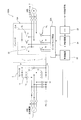
- the motor control device 100 includes a converter 2 connected to the three-phase AC power source 1 and an inverter 5 connected to the motor 3 and also connected to the converter 2 via the DC bus 4.
- the converter 2 includes a rectifying unit 11 and a smoothing capacitor 12.
- the rectifying unit 11 is a diode bridge composed of six diodes 13, and full-wave rectifies the AC power from the three-phase AC power supply 1 and outputs it to the DC bus 4.
- the smoothing capacitor 12 is connected so as to pass between the DC buses 4, and smoothes the DC power that has been full-wave rectified by the rectifying unit 11.
- the converter 2 rectifies and smoothes the AC power supplied from the three-phase AC power source 1 to convert it into DC power, and consists of a set of two, a positive-side P line and a negative-side N line. DC power is output to the DC bus 4.
- the inverter 5 includes a bridge circuit 21, a gate drive circuit 22, a control power source 23, a control circuit 24, and an I / O 25.
- the inverter 5 corresponds to an inverter circuit described in each claim.
- the bridge circuit 21 is a device in which six arm switching elements 31 formed of a semiconductor such as an IGBT, a MOSFET, and a HEMT are bridge-connected. Specifically, two arm switching elements 31 configured by connecting a semiconductor switching element 32 and a diode 33 which is a flywheel diode (FWD) in parallel are connected in series to form one set, and three sets of the DC bus 4 are connected to the DC bus 4. They are connected in parallel.
- the arm switching element 31 connected to the positive electrode side of the DC bus 4 (P line side) is referred to as an upper arm switching element Q H, lower arm arm switching element 31 connected to the negative (N line side) that the switching element Q L.
- Each arm switching element 31 switches its conduction state (ON state) and cutoff state (OFF state) by controlling the gate-source voltage Vgs by the gate drive circuit 22.
- the gate drive circuit 22 controls the gate-source voltage Vgs for each arm switching element 31 of the bridge circuit 21 based on a switching control signal input from the control circuit 24 described later, thereby turning the gate drive circuit 22 on and off. Switch.
- a specific circuit configuration of the gate drive circuit 22 provided in the present embodiment will be described in detail later with reference to FIG.
- the control circuit 24 is configured by a CPU or the like that executes software for power control, and based on a motor control command input from a host control device (not shown) via the I / O 25 or a signal input circuit (not shown).
- a switching control signal is output to the gate drive circuit 22 so as to supply desired power to the motor 3.
- This switching control signal is output by PWM control corresponding to the motor control command, and the DC power between the DC buses 4 is supplied to each arm switching element 31 of the bridge circuit 21 from the intermediate connection position of each set.
- the gate drive circuit 22 is controlled so as to output corresponding to each phase of the three-phase AC motor 3.
- Control power supply 23 (corresponding to a drive power supply) is connected to, for example, two phases of the three-phase AC power supply 1 to supply power to each part in the inverter 5.
- FIG. 2 shows an enlarged connection configuration of a pair of upper arm switching element Q H and lower arm switching element Q L in the bridge circuit 21.
- each of the arm switching elements Q H and Q L includes a semiconductor switching element 32 having three electrodes of a drain electrode 41, a source electrode 42, and a gate electrode 43, and a drain electrode from the source electrode 42 side.
- the flywheel diode 33 is connected in parallel to the semiconductor switching element 32 with the direction toward the 41 side as a forward direction.
- the source electrode 42 of the upper arm switching element Q H and the drain electrode 41 of the lower arm switching element Q L are connected, and the upper and lower arm switching elements Q H and Q L are connected in series.
- Each of the arm switching elements Q H and Q L switches between conduction and interruption (ON and OFF) between the drain electrode 41 and the source electrode 42 by the gate-source voltage Vgs.
- the gate-source voltage Vgs is a relative potential difference of the potential of the gate electrode 43 with respect to the potential of the source electrode 42, and becomes a positive bias when the potential of the gate electrode 43 is higher than the potential of the source electrode 42.
- a negative bias occurs when the potential of the gate electrode 43 is lower than the potential.
- conduction occurs when the gate-source voltage Vgs is applied with a positive bias voltage higher than a predetermined value (higher than the so-called gate threshold voltage).
- the state is turned off (OFF state).
- the gate drive circuit 22 that performs switching control of the arm switching elements Q H and Q L as described above, the potential relationship between the control line 51 connected to the gate electrode 43 and the electrode line 52 connected to the source electrode 42 is high. The switching between the ON state and the OFF state is controlled by switching.
- inter-terminal capacitances potentially exist between the drain electrode 41 and the gate electrode 43 and between the source electrode 42 and the gate electrode 43, respectively.
- the A current flows in the inter-terminal capacitance (Cgd in the figure) between the drain electrode 41 and the gate electrode 43 to be charged, and further, the inter-terminal capacitance between the source electrode 42 and the gate electrode 43 due to the influence thereof. Also in (Cgs in the figure), a current flows and charges.
- FIG. 3 shows only the portion of the gate drive circuit 22E that connects to one of the lower arm switching element Q L (hereinafter, the same in each drawing corresponding).
- the gate drive circuit 22E of the comparative example shown feed terminal 61, control terminal 62, and a drive IC53 including a ground terminal 63, control terminal 62 and the lower arm switching element Q control line 51 for connecting the gate electrode 43 of the L
- a first gate resistor Rg1 provided on the control line 51 a connection line 71 connecting the power supply terminal 61 and the ground terminal 63, and an electrode line connecting the connection point 72 on the connection line 71 and the source electrode 42.
- a bias resistor R1 provided to be connected between the control line 51 and the electrode line 52, a bias resistor R1 provided to be connected between the control line 51 and the electrode line 52, a limiting resistor Rzd provided between the feeding terminal 61 and the connection point 72 on the connection line 71, and a connection line 71, a Zener diode ZD provided between the connection point 72 and the ground terminal 63, a parallel line 73 connected in parallel between both terminals of the Zener diode ZD, and the parallel line 7 3 has a negative bias capacitor C1 (corresponding to a first capacitor) and a bypass capacitor C2 provided in parallel with the connection line 71 so as to be connected between the power supply terminal 61 and the ground terminal 63.
- the drive IC 53 has one changeover switch 64 inside. Based on the switching control signal S from the control circuit 24, the changeover switch 64 is connected to the terminal 64a to which positive potential power (+ Vcc) is always supplied from the drive power supply (corresponding to the control power supply 23; not shown) and the control. The conduction state and the cutoff state between the terminal 64b connected to the terminal 62 are switched. When the switching control signal S is turned ON, the changeover switch 64 is turned on, and a potential of the power supply potential + Vcc (hereinafter referred to as a high level) is added to the control line 51.
- a potential of the power supply potential + Vcc hereinafter referred to as a high level
- the changeover switch 64 When the switching control signal S is output OFF, the changeover switch 64 is cut off and the control line 51 becomes substantially zero potential (substantially equivalent to the GND ground potential; hereinafter referred to as low level).
- the power supply terminal 61 is always supplied with a power supply potential + Vcc from the drive power supply, and the ground terminal 63 is grounded to GND and always maintains substantially zero potential.
- First gate resistor Rg1 is arranged by the slew rate of the lower arm switching element Q L between the gate electrode 43 of the control terminal 62 and the lower arm switching element Q L Drive IC53 on the control line 51 as described above This is a resistor for adjusting (dV / dt).
- the “arrangement” means not a physical arrangement between the component parts on the actual board but an arrangement as a connection relationship on the circuit (the same applies hereinafter).
- the bias resistor R1 is a pull-down resistor, and has a resistance value such that a current of about several mA flows to the bias resistor R1 in order to maintain the gate-source voltage Vgs1 at the time of off at the potential of the connection point 72.
- the bypass capacitor C2 is a noise removing capacitor.
- the limiting resistor Rzd is a resistor provided to appropriately limit a current flowing in a Zener diode ZD described later.
- the zener diode ZD is a so-called constant voltage diode that becomes conductive when the reverse voltage exceeds a predetermined breakdown voltage.
- the direction from the ground terminal 63 to the power supply terminal 61 is a forward direction on the connection line 71. Is arranged.
- the positive voltage + Vcc exceeding the breakdown voltage is supplied from the power supply terminal 61, so that the negative bias capacitor C1 connected in parallel to the Zener diode ZD is charged with a voltage equivalent to the breakdown voltage.
- the Zener A potential difference (+ Vzd) equivalent to the breakdown voltage is always maintained between both terminals of the diode ZD. That is, in the gate drive circuit 22E of this comparative example, a potential of + Vzd is always applied to the source electrode 42 connected to the connection point 72 through the electrode line 52.
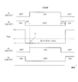
- FIG. 4 is a time chart of various switching states and the gate-source voltage Vgs L in one set of arm switching elements Q H and Q L in the bridge circuit 21 to which the gate drive circuit 22E of the comparative example configured as described above is connected. Shown in In this figure 4, the switching state of the switching control signal S H corresponding to the upper arm switching element Q H from the top (ON / OFF), switching state of the switching control signal S L corresponding to the lower arm switching element Q L (ON / OFF) and the voltage Vgs L between the gate and source of the lower arm switching element Q L, the switching state of the upper arm switching element Q H and (ON / OFF), switching state of the lower arm switching element Q L (ON / OFF) shows an example of a time-series change.
- a normally-off type semiconductor switching element 32 is used for each of the arm switching elements Q H and Q L , and the positive bias voltage and the negative bias voltage of the gate-source voltage Vgs are +10 V and ⁇ 5 V, respectively.
- the positive bias voltage + 10V and the negative bias voltage -5V are set assuming that the semiconductor switching element 32 is formed of, for example, a GaN-HEMT device. In this case, the appropriate positive bias voltage and negative bias voltage may be set.
- the PWM control in the control circuit 24, arm switching element Q H and the lower arm switching element Q L on the same set are switched controlled to be ON state alternately.
- the ON periods in the respective switching control signals S H and S L are surely prevented so that the upper arm switching element Q H and the lower arm switching element Q L are simultaneously turned on and the DC bus 4 is not short-circuited.
- the dead time DT for setting both to the OFF state is set to the same time between the ON period and the ON period (from one turn-off to the other turn-on).
- the upper arm switching element Q H is in the OFF state, and the lower arm switching element Q L is further turned on. It is necessary to control so as to be a positive bias voltage (+10 V in this example) only during the period in which it should be turned on. Further, with respect to the gate-source voltage Vgs L applied to the lower arm switching element Q L , the upper arm switching element Q H including the dead time DT is turned on, that is, the lower arm switching element Q L is It is necessary to perform control so that the voltage is substantially 0 voltage or less only during the period in which the switch is to be turned off.
- the potential is applied to the gate electrode 43 of the lower arm switching element Q L by the mirror effect immediately after turn-on of the upper arm switching element Q H A (hereinafter, referred to as self-turn-on potential) is the offset to the negative bias voltage -Vzd , it is possible to prevent the self turn-on of the lower arm switching element Q L.
- the positive bias voltage of the gate-source voltage Vgs L is also the source voltage ⁇ Vs L added to the source electrode 42, that is, the negative bias voltage ⁇ Vzd. Is offset.
- the gate voltage Vg output from the control terminal 62 to the gate electrode 43 is obtained.
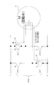
- FIG. 6 shows a circuit configuration of the gate drive circuit 22 of the present embodiment that realizes such an operation.
- the difference from the gate drive circuit 22E of the comparative example shown in FIG. 3 is that the gate drive circuit 22 of this embodiment shown in FIG. 6 is further provided so as to control short circuit or interruption between both terminals of the Zener diode ZD.
- the first auxiliary switching element Q1 (corresponding to the first auxiliary element) provided, and the second auxiliary switching element Q2 (corresponding to the second auxiliary element) provided to control the conduction or blocking of the parallel line 73.
- the gate electrodes (corresponding to the first auxiliary gate electrode and the second auxiliary gate electrode) of these two auxiliary switching elements Q1 and Q2 have a common second gate resistance Rg2 for adjusting the slew rate (dV / dt). To the control line 51.
- the resistor Rg2 constitutes the negative bias circuit unit 54.
- the negative bias circuit section 54 corresponds to means configured to switch between addition and non-addition of the negative bias potential described in each claim.
- the first auxiliary switching element Q1 is a normally-off type semiconductor switching element composed of, for example, an N-channel MOS, and when the gate voltage Vg (corresponding to a gate control signal) is at a high level, that is, the supply potential to the control line 51. When a potential of + Vcc (corresponding to a predetermined positive potential) is applied, both terminals of the Zener diode ZD are short-circuited.
- the second auxiliary switching element Q2 is a normally-on type semiconductor switching element constituted by, for example, a P-channel MOS, and cuts off the parallel line 73 when the gate voltage Vg is at a high level.
- the potential at the connection point 72 is the charge potential of the negative bias capacitor C1: is added to (Vzd corresponding to a predetermined potential difference), and the source electrode 42 of the negative bias potential is lower arm switching element Q L corresponding thereto .
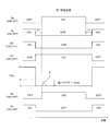
- FIG. 9 shows a time chart of various switching states and the gate-source voltage Vgs L in the case of the gate drive circuit 22 of the present embodiment that operates as described above.
- the switching states (ON / OFF) of the first auxiliary switching element Q1 and the second auxiliary switching element Q2 are also shown.
- the behavior waveform of the first auxiliary switching element Q1 is the switching control signal S. L and becomes approximately the same behavior waveform of the second auxiliary switching element Q2 is almost opposite phase as the switching control signal S L and the first auxiliary switching element Q1.
- it has the same behavior waveform as the time chart shown in FIG. 4, that is, in the gate drive circuit 22 of this embodiment, the self-turn-on potential A is canceled by the negative bias voltage as in the comparative example, Self-turn-on can be prevented.
- the gate voltage Vg L is at the low level only while the switching control signal SL is output OFF.
- a negative bias potential is applied to the source electrode 42 only in the meantime, and the gate-source voltage Vgs L is offset by the negative bias voltage ⁇ Vzd.
- the switching control signal SL is ON, that is, while the gate voltage Vg L is at the high level, the source electrode 42 becomes substantially zero potential, and the gate-source voltage Vgs L is not offset.
- the positive bias of the gate-source voltage Vgs L can be obtained only by outputting the gate voltage Vg L (+10 V in this example) corresponding to the positive bias voltage from the control terminal 62 while the switching control signal SL is ON.
- the voltage can be secured sufficiently higher than the gate threshold voltage Vth (in this example, +10 V is secured). That is, in the present embodiment, the GND ground potential (substantially 0 potential) and the negative bias potential ( ⁇ Vzd) are switched and added to the source electrode 42 in accordance with the gate voltage Vg L , thereby driving more than the case of the comparative example.
- the required supply voltage (+ Vcc) of the power supply can be suppressed, and the overall circuit scale can be saved.
- normally the type of semiconductor switching elements on the lower arm switching element Q L 32 may be applied.
- the first auxiliary switching element Q1 to a normally-on type
- the second auxiliary switching element Q2 to a normally-off type
- functions equivalent to those of the above embodiment can be obtained (not shown).
- the switching control signal S L is output to ON
- the lower arm switching element Q L is turned off
- the switching control signal S L is output to OFF
- the lower arm switching element Q L is turned on. It becomes.
- first bridge circuit 21 six arm switching element Q H provided is by all OFF state arm switching element Q H on the phase of the Q L, DC The vertical short circuit between the buses 4 and the power supply to the motor 3 are blocked.
- each of the arm switching elements Q H and Q L is normally off or normally on by repeatedly switching each of the lower arm switching elements Q L to ON / OFF according to the operation of the PWM control.
- the negative bias capacitor C1 can be charged in the same manner.
- the all OFF state lower arm switching element Q L of each phase after the lower stage charge completion repeated several times to switch the ON / OFF in compliance with the operation of the PWM control for each of the upper arm switching element Q H therebetween The upper stage can be charged.
- N a ⁇ f ⁇ Rzd ⁇ C1 (1)
- a a coefficient
- f a carrier frequency of PWM control
- Rzd a resistance value of the limiting resistor Rzd
- C1 a capacity of the negative bias capacitor C1.
- the value of Rzd ⁇ C1 corresponds to a time constant until the negative bias capacitor C1 reaches about 63% of the breakdown voltage Vzd of the Zener diode ZD.
- the value of the coefficient a is set to It may be desirable to set it to 2 or more.
- the voltage between both terminals of the negative bias capacitor C1 can be charged to be equal to the breakdown voltage Vzd of the Zener diode ZD by repeating switching at a realistic number of times such as about 150 times.
- each arm switching element Q L may perform switching of each arm switching element Q L simultaneously in the same lower side, or may be performed individually.
- the lower side may be charged after the upper side is charged first.
- a negative bias circuit unit 54 configured to switch and add a ground potential (approximately 0 potential) and a negative bias potential ( ⁇ Vzd) is provided.
- the source electrode 42 only adds a negative bias potential when necessary in accordance with the potential of the gate voltage Vg L, it can be substantially zero potential otherwise. That in preventing self turn-on phenomenon the lower arm switching element Q L as OFF state, may be added a negative bias potential to the source electrode 42.
- the gate voltage Vg L outputs at a potential just exceeds the gate threshold voltage Vth Only a sufficient positive bias voltage of the gate-source voltage Vgs L can be ensured, that is, the supply voltage (+ Vcc) of the drive power supply can be reduced. As a result, it is possible to save the circuit scale of the entire gate drive circuit 22 and thus the motor control apparatus 100 as a whole.
- the lower arm switching element Q L when the lower arm switching element Q L is a so-called normally-off type, when the ON state to the gate voltage Vg L to the high level (predetermined positive potential). Further, when the OFF state is set, the gate voltage Vg L is set to a low level (substantially 0 potential).
- the negative bias circuit 54 adds a substantially zero potential with respect to the source electrode 42 when the time the lower arm switching element Q L is in the ON state, i.e. the gate voltage Vg L is at the high level .
- the gate voltage Vg L can be secured at a potential sufficient to exceed the gate threshold voltage Vth, so that a sufficient positive bias voltage of the gate-source voltage Vgs L can be secured, that is, the supply voltage of the drive power supply can be reduced.
- the negative bias circuit portion 54 is configured such that when the lower arm switching element Q L is in the cut-off state, that is, when the gate voltage Vg L is at a low level, A negative bias potential (+ Vzd) is applied so as to increase with a potential difference exceeding the self-turn-on potential A.
- the self turn-on potential A applied to the gate electrode 43 due to the mirror effect can be canceled and the self turn-on phenomenon can be prevented.
- gate drive circuit 22 corresponding to the lower arm switching element Q L the present invention is not limited thereto.
- the present invention is not limited thereto.
- the gate drive circuit 22 can be applied.
- the negative bias circuit unit 54 uses the charging potential charged from the drive power supply when the gate voltage Vg is at a high level as the negative bias potential when the gate voltage Vg is at a low level. It is added to the source electrode 42. Accordingly, the negative bias circuit unit 54 can generate a negative bias potential and apply it to the source electrode 42 when necessary without preparing a separate power source independent of the drive power source, thereby simplifying the circuit configuration.
- the drive IC 53 is connected to the power supply terminal 61 that outputs the positive power supply potential (+ Vcc) from the drive power supply and the gate electrode 43 via the control line 51 and supplies the gate voltage Vg.
- the negative bias circuit unit 54 includes a control terminal 62 that switches between a high level of a positive potential and a low level of a substantially zero potential, and a ground terminal 63 that holds a ground ground potential of a substantially zero potential.
- a Zener diode ZD having a predetermined breakdown voltage (Vzd) with a direction from the ground terminal 63 toward the power supply terminal 61 as a forward direction, and a parallel line connecting between both terminals of the Zener diode ZD With 3 disposed on a negative bias capacitor C1, the first auxiliary switching element Q1 which is configured to control the short-circuit or blocking between both terminals of the Zener diode ZD, a.
- the parallel circuit of the Zener diode ZD and the negative bias capacitor C1 generates and holds a negative bias potential, and the first auxiliary switching element Q1 applies the negative bias potential to the source electrode 42. It is possible to realize the operation of switching between non-addition (grounding).
- the negative bias circuit unit 54 includes the second auxiliary switching element Q2 configured to control conduction or interruption of the parallel line 73, thereby generating a negative bias potential. It is possible to prevent the charging potential of the bias capacitor C1 from being unnecessarily discharged.
- the first auxiliary switching element Q1 is a normally-off type semiconductor switching element
- the second auxiliary switching element Q2 is a normally-on type semiconductor switching element
- each of the auxiliary switching elements Q1, Q2 A gate electrode is connected to the control line 51.
- the circuit configuration of the entire motor control device 100A according to the second embodiment will be described with reference to FIG.
- the difference from the motor control device 100 shown in FIG. 1 is that all the arm switching elements Q H and Q L provided in the bridge circuit 21A of the inverter 5A are not provided with the flywheel diode 33, but are semiconductors. It is in the point which comprises only the switching element 32.
- the semiconductor switching element 32 composed of a GaN-FET having a parasitic diode 34 with poor characteristics
- the mounting area increases particularly when the flywheel diode 33 is provided.
- the inverter 5A, particularly the bridge circuit 21A has a configuration in which the flywheel diode 33 is omitted as described above in order to achieve small and high-density mounting for the purpose of improving frequency characteristics.
- the parasitic diode 34 potentially included in the semiconductor switching element 32 has a forward direction from the source electrode 42 to the drain electrode 41, and has characteristics depending on the material constituting the semiconductor switching element 32 and the internal circuit configuration. It is very different.
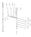
- FIG. 13 shows the voltage-current characteristics of a flywheel diode 33 (equivalent to a normal diode) connected in reverse parallel to a general IGBT semiconductor switching element 32.
- a forward current does not flow unless a voltage exceeding a certain forward voltage Vf is applied to the forward direction. Note that only the forward voltage region is focused here, and the leakage current and breakdown phenomenon in the reverse voltage region are ignored.
- the voltage-current characteristic of the semiconductor switching element 32 (not provided with the flywheel diode 33) formed of a GaN-FET having a parasitic diode 34 with poor characteristics is as shown in FIG.
- the reverse current is only applied when the reverse voltage (Vsd ⁇ 0) is added to the source-drain voltage Vsd. (Ids ⁇ 0) flows, that is, a current flows in a direction from the source electrode 42 to the drain electrode 41 via the parasitic diode 34 (see the lower left region in the drawing).
- the forward voltage Vf in this case, the reverse current flows in the parasitic diode 34 in proportion to the magnitude of the negative bias voltage added to the gate-source voltage Vgs. Therefore, the minimum required reverse source-drain voltage Vsd) is increased.
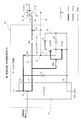
- the semiconductor switching element 32 that potentially includes the parasitic diode 34 having poor characteristics as described above, when the regenerative current is refluxed with the negative bias voltage applied, the semiconductor switching element 32 has such a large conduction that it cannot be neglected. Loss (power consumption during conduction) occurs. That is, as shown in FIG. 15 corresponds to FIG. 9, in the dead time period DT in which both of the upper arm switching element Q H and the lower arm switching element Q L is turned OFF, the return current Ids is reverse current Flows. At the same time, during the dead time period DT, a reverse potential difference ( ⁇ Vfv) corresponding to the forward voltage Vf of the parasitic diode 34 is generated with a magnitude proportional to the negative bias voltage as the source-drain voltage Vds.
- ⁇ Vfv reverse potential difference
- dead time loss P Ids ⁇ (Vds + Vgs) proportional to the negative bias voltage added to the gate-source voltage Vgs occurs.
- the gate drive circuit 22A of the second embodiment is provided with the negative bias circuit section 54A having the circuit configuration shown in FIG. 16, thereby reducing the dead time loss.
- the difference from the negative bias circuit section 54 of the first embodiment shown in FIG. 6 is that the negative bias circuit section 54A of the second embodiment shown in FIG. 16 further grounds the control line 51, It has a time constant resistor R2 (first resistor) and a time constant capacitor C3 (second capacitor) arranged in series on the ground line 74, and the gate electrodes of the two auxiliary switching elements Q1, Q2 are common.
- the time constant resistor R and the time constant capacitor C are connected to the ground line 74 via the second gate resistor Rg2 and further connected to the control line 51 via the time constant resistor R2 on the ground line 74. Is different. Other parts are the same as those in the first embodiment, and the description thereof is omitted.
- the state is switched through four steps I to IV during one operation cycle (in one carrier cycle of PWM control).
- the switching control signal S is ON
- the first process I is in a state as shown in FIG. Even in this case, it is assumed that the negative bias capacitor C1 and the time constant capacitor C3 are charged in advance by the initial charging sequence.
- a first step I illustrated in FIG. 17 the control terminal 62 of the drive IC53 by the switching control signal S is ON output is added supply potential + Vcc, high to the gate electrode 43 of the lower arm switching element Q L A level gate voltage Vg is added.
- the first auxiliary switching element Q1 is turned on to short-circuit both terminals of the Zener diode ZD, and the second auxiliary switching element.
- Q2 cuts off the parallel line 73 to prevent the negative bias capacitor C1 from discharging. Accordingly, the potential at the connection point 72 becomes the GND ground potential, a substantially zero potential is added to the source electrode 42 of the lower arm switching element Q L.
- the switching control signal S is ON output, the positive bias voltage (+ Vcc) is added to the gate-source voltage Vgs of the lower arm switching element Q L, the lower arm switching element Q L Is turned on (equivalent to the state shown in FIG. 7).
- the gate voltage Vg is at a low level
- the gate electrode potentials of the auxiliary switching elements Q1 and Q2 are maintained at a high level because the time constant capacitor C3 is in a charged state.
- the conduction state of the first auxiliary switching element Q1 and the cutoff state of the second auxiliary switching element Q2 are maintained.
- the state of the third step III as shown in FIG. 19 is entered. That is, as the discharge of the time constant capacitor C3 proceeds, the gate potentials of the auxiliary switching elements Q1 and Q2 are also set to the same low level as the gate voltage Vg, so that the first auxiliary switching element Q1 is switched to the cut-off state. 2
- the auxiliary switching element Q2 is switched to the conductive state. That is, the parallel circuit of the Zener diode ZD and the negative bias capacitor C1 functions effectively so that the potential at the connection point 72 becomes the charging potential (Vzd) of the negative bias capacitor C1, and the negative bias potential corresponding to this becomes the lower arm switching. It is added to the source electrode 42 of the element Q L.
- the third step III is a stable period after switching the switching control signal S to the OFF output, a negative bias voltage (-Vzd) is added to the gate-source voltage Vgs of the lower arm switching element Q L, the lower arm switching element Q L is turned OFF (equivalent to the state of FIG. 8).
- the timing for switching from the second step II to the third step III can be arbitrarily set by adjusting the time constant determined by the time constant resistor R2 and the time constant capacitor C3.
- the gate voltage Vg is high level
- the gate electrode potentials of the auxiliary switching elements Q1 and Q2 are low level while the time constant capacitor C3 discharged during the third step III is not yet fully charged.
- the cutoff state of the first auxiliary switching element Q1 and the conduction state of the second auxiliary switching element Q2 are maintained.
- the negative bias potential corresponding to the charge potential of the negative bias capacitor C1 (Vzd) is added to the source electrode 42 of the lower arm switching element Q L.
- the gate-source voltage Vgs of the lower arm switching element Q L differential voltage of the positive bias voltage and a negative bias voltage (+ Vcc-Vzd) is Added. If the absolute value of the power supply potential + Vcc is sufficiently larger than the absolute value of the charging potential Vzd of the negative bias capacitor C1, as a result, a positive bias voltage exceeding the gate threshold voltage Vth is added to the gate-source voltage Vgs. it can be, the lower arm switching element Q L is turned ON.
- the fourth process IV is a process with a relatively short period of time because the process proceeds to the first process I when the time constant capacitor C3 is sufficiently charged.
- FIG. 21 shows time charts of various switching states and the gate-source voltage Vgs L in the case of the gate drive circuit 22A of the second embodiment that operates through the above-described steps I to IV.
- the potential Vs of the source electrode 42 is maintained at substantially 0 potential only during LT (corresponding to a predetermined time), and approximately 0 voltage is added to the gate-source voltage Vgs L (no negative bias voltage is added; second step) II).
- the time constant capacitor C3 is discharged and the two auxiliary switching elements Q1 and Q2 are switched between ON / OFF states, whereby the potential Vs of the source electrode 42 is changed to the gate electrode 43. That is, a negative bias voltage of ⁇ Vzd ( ⁇ 5 V in this example) is added to the gate-source voltage Vgs L (third step III). In this state, the self turn-on potential A is offset by a negative bias voltage -Vzd, it is possible to prevent the self turn-on phenomenon in the first embodiment similarly to the lower arm switching element Q L.
- the time constant period LT is set to substantially the same period as the dead time DT, and the process shifts from the second process II to the third process III before the generation of the self-turn-on potential A, so that at least the time constant period.
- the time constant period LT elapses after the negative bias circuit unit 54A has changed from the gate voltage Vg to the low level. Later, a negative bias potential is added to the gate-source voltage Vgs.
- the semiconductor switching element Q L is Until constant period LT elapses when from when the OFF state of the forward voltage Vf of the parasitic diode 34 without being added negative bias voltage to the semiconductor switching element Q L It is possible to suppress the increase and reduce the dead time loss P.
- the time constant period LT is set within a required time from when the gate voltage Vg becomes low level until the self-turn-on potential A due to the mirror effect is applied to the gate electrode 43. Yes. Thereby, since a negative bias voltage can be applied before the occurrence of the self-turn-on phenomenon, both the reduction of the dead time loss P and the prevention of the self-turn-on phenomenon can be achieved.
- the negative bias circuit unit 54A includes the ground line 74 that grounds the control line 51, and the time constant resistor R2 and the time constant capacitor C3 that are arranged in series on the ground line 74.
- the gate electrodes of the two auxiliary switching elements Q1 and Q2 are connected to the ground line 74 between the time constant resistor R2 and the time constant capacitor C3, and are connected to the control line 51 via the ground line 74.
- the time constant period LT can be arbitrarily set by adjusting the time constants of the time constant resistor R2 and the time constant capacitor C3.
- the dead time loss P can be reduced when a GaN-FET (normally on) having a parasitic diode 34 with poor characteristics as shown in FIG. 14 is used as the semiconductor switching element 32. It is useful as, but is not limited to this.
- the second embodiment may be applied even when Si-MOSFET, SiC-MOSFET, and GaN-HEMT including the parasitic diode 34 with good characteristics are used as the semiconductor switching element 32. .
- the flywheel diode 33 is installed and the first bias circuit section 54A including the negative bias circuit section 54A is installed. Two embodiments may be applied.
- the gate structure of the semiconductor switching element is a current type>
- a semiconductor switching element 32 having a gate structure of a current type similar to that of a transistor, such as GaN-GIT is used for the arm switching elements Q H and Q L , the conduction resistance of the gate electrode 43 increases and power is increased. Loss (switching loss) tends to increase. This can be solved by applying a gate drive circuit 22B having a circuit configuration as shown in FIG.
- the series circuit of the third gate resistor Rg3 and the gate capacitor C4 is compared with the gate drive circuit 22A of the second embodiment shown in FIG. It is different in that it is connected in parallel to one gate resistor Rg1, and an intermediate point between the third gate resistor Rg3 and the gate capacitor C4 is connected to the discharge terminal 65 of the drive IC 53B via the fourth gate resistor Rg4. Yes. Further, the drain terminal 65 of the drive IC 53B is configured to be grounded when the switching control signal S is output OFF.
- the gate drive circuit 22B when the switching control signal S is output ON, the gate voltage Vg from the control terminal 62 becomes high level and the lower arm switching is performed through the low impedance gate capacitor C4. it is charged and the potential of the gate electrode 43 of the element Q L, can be switched on immediately oN state lower arm switching element Q L. Thereafter, the current can be continuously supplied to the gate electrode 43 through the first gate resistor Rg1 to maintain the low conduction resistance of the gate electrode 43. That is, the turn-on operation of the semiconductor switching element 32 can be accelerated and the switching loss can be reduced.
Landscapes
- Engineering & Computer Science (AREA)
- Power Engineering (AREA)
- Inverter Devices (AREA)
- Power Conversion In General (AREA)
Abstract
半導体スイッチング素子(32)の導通または遮断を制御するように構成されたゲートドライブ回路(22)は、半導体スイッチング素子(32)のゲート電極(43)に対して、当該半導体スイッチング素子(32)の導通または遮断を制御するゲート電圧Vgを出力するように構成されたドライブIC(53)と、ゲート電圧Vgの電位に応じて、半導体スイッチング素子(32)のソース電極(42)に対し略0電位と負バイアス電位を切り替えて付加するように構成された負バイアス回路部(54)と、を有する。これにより、回路規模の省力化を可能とする。
Description
開示の実施形態は、ゲートドライブ回路、インバータ回路、及びモータ制御装置に関する。
特許文献1には、例えばGaN-FETのように寄生ダイオードを持たないノーマリオフタイプの半導体スイッチング素子における安定動作と回生時の電力損失を低減させるためのスイッチング回路の構成が開示されている。
例えばFET等の半導体スイッチング素子においては、ドレイン電極とゲート電極の間、及びソース電極とゲート電極の間のそれぞれに寄生容量が潜在的に存在する。このため、周辺回路の影響によりドレイン電極またはソース電極のいずれか一方の電位が急激に上昇(dV/dt大)した場合には、ミラー効果によって両側の寄生容量が充電してゲート電極の電位が上昇し、その結果ゲート電極の電位が作動閾値を超えて当該半導体スイッチング素子が強制的に接続状態(縦短絡)にさせられるセルフターンオン現象を発生してしまう。
このようなセルフターンオンを防止する対策として、ミラー効果によるゲート電位の上昇前に当該半導体スイッチング素子のゲートソース間に負バイアス電圧を付加する手法が考えられる。しかし上記従来技術ではこのような負バイアスを付加する構成を備えておらず、また負バイアスを付加するためにはその分の電位を確保できるよう供給電圧の高いドライブ用電源を用意する必要があり、それだけ全体の回路規模が大型化してしまう。
本発明はこのような問題点に鑑みてなされたものであり、回路規模の省力化が可能なゲートドライブ回路、インバータ回路、及びモータ制御装置を提供することを目的とする。
上記課題を解決するため、半導体スイッチング素子の導通または遮断を制御するように構成されたゲートドライブ回路であって、前記半導体スイッチング素子のゲート電極に対して、当該半導体スイッチング素子の導通または遮断を制御するゲート制御信号を出力するように構成されたゲート制御部と、前記ゲート制御信号の電位に応じて、前記半導体スイッチング素子のソース電極に対し略0電位と負バイアス電位を切り替えて付加するように構成された負バイアス回路部と、を有するゲートドライブ回路が適用される。
また、本発明の別の観点によれば、半導体スイッチング素子の導通または遮断を制御するゲートドライブ回路であって、負バイアス電位の付加と無付加を切り替えるように構成された手段を有するゲートドライブ回路が適用される。
また、本発明の別の観点によれば、モータへ電力を給電するインバータ回路であって、前記半導体スイッチング素子を2つ直列に接続した組を直流母線間に複数並列に接続したブリッジ回路と、前記ブリッジ回路における複数の前記半導体スイッチング素子の導通または遮断をそれぞれ制御するように構成された請求項1乃至10のいずれか1項に記載のゲートドライブ回路と、を有するインバータ回路が適用される。
また、本発明の別の観点によれば、モータを駆動するモータ制御装置であって、請求項11に記載のインバータ回路と、交流電源からの交流電圧を直流電圧に整流して前記直流母線に給電するように構成された整流部と、前記整流部で整流された前記直流母線間の直流電圧を平滑するように構成された平滑コンデンサと、を有するモータ制御装置が適用される。
本発明によれば、回路規模の省力化が可能となる。
<第1実施形態>
以下、第1の実施の形態について図面を参照しつつ説明する。
以下、第1の実施の形態について図面を参照しつつ説明する。
<第1実施形態のモータ制御装置の概略構成>
まず、図1を用いて、本実施形態に係るモータ制御装置全体の回路構成について説明する。図1に示すように、モータ制御装置100は、3相交流電源1に接続するコンバータ2と、モータ3に接続するとともに直流母線4を介してコンバータ2にも接続するインバータ5を備える。
まず、図1を用いて、本実施形態に係るモータ制御装置全体の回路構成について説明する。図1に示すように、モータ制御装置100は、3相交流電源1に接続するコンバータ2と、モータ3に接続するとともに直流母線4を介してコンバータ2にも接続するインバータ5を備える。
コンバータ2は、整流部11と、平滑コンデンサ12とを備えている。整流部11は、6つのダイオード13からなるダイオードブリッジであり、3相交流電源1からの交流電力を全波整流して直流母線4に出力する。平滑コンデンサ12は、直流母線4間を渡すように接続され、上記整流部11が全波整流した直流電力を平滑する。以上の構成によって、コンバータ2は、3相交流電源1から供給される交流電力を整流、平滑して直流電力に変換し、正極側のP線及び負極側のN線の2本1組からなる直流母線4に直流電力を出力する。
インバータ5は、ブリッジ回路21と、ゲートドライブ回路22と、制御電源23と、制御回路24と、I/O25とを備えている。なお、このインバータ5が、各請求項記載のインバータ回路に相当する。
ブリッジ回路21は、例えばIGBT、MOSFET、HEMTなどの半導体で構成する6つのアームスイッチング素子31をブリッジ接続したデバイスである。詳しくは、半導体スイッチング素子32とフライホイールダイオード(FWD)であるダイオード33とを並列接続して構成したアームスイッチング素子31を2つ直列に接続して1組とし、上記直流母線4に対して3組並列に接続している。そのうち、以下では、直流母線4の正極側(P線側)に接続するアームスイッチング素子31を上アームスイッチング素子QHといい、負極側(N線側)に接続するアームスイッチング素子31を下アームスイッチング素子QLという。3組それぞれにおける上アームスイッチング素子QHと下アームスイッチング素子QLの間の中間点が、各相に対応してモータ3に接続されている。各アームスイッチング素子31は、それぞれのゲートソース間電圧Vgsをゲートドライブ回路22により制御されることでその導通状態(ON状態)と遮断状態(OFF状態)を切り替える。
ゲートドライブ回路22は、後述の制御回路24から入力される切替制御信号に基づき、ブリッジ回路21の各アームスイッチング素子31に対しそれぞれのゲートソース間電圧Vgsを制御することでそのON状態とOFF状態を切り替える。なお、本実施形態が備えるゲートドライブ回路22の具体的な回路構成については後に図6を用いて詳述する。
制御回路24は、電力制御用のソフトウェアを実行するCPU等で構成されており、図示しない上位制御装置からI/O25や図示しない信号入力回路等を介して入力されるモータ制御指令に基づいて、モータ3に所望の電力を供給するようゲートドライブ回路22に切替制御信号を出力する。この切替制御信号は上記モータ制御指令に対応するPWM制御により出力されるものであり、ブリッジ回路21の各アームスイッチング素子31に対してそれぞれ直流母線4間の直流電力を各組の中間接続位置から3相交流モータ3の各相に対応して出力させるようゲートドライブ回路22を制御する。ブリッジ回路21の各組においては、同じ組の上アームスイッチング素子QHと下アームスイッチング素子QH,QLを同時に導通させると上アームスイッチング素子QHと下アームスイッチング素子QLに大電流が流れて両アームスイッチング素子31を損傷させてしまう。このような直流母線4間の短絡を防ぐために上記PWM制御では、同じ組の上アームスイッチング素子QHと下アームスイッチング素子QLを同時に導通させることがないよう切替制御信号を出力する。
制御電源23(ドライブ用電源に相当)は、例えば3相交流電源1の2相に接続してインバータ5内の各部に電力を供給する。
<アームスイッチング素子の動作とセルフターンオンについて>
図2は、ブリッジ回路21における1組の上アームスイッチング素子QHと下アームスイッチング素子QLの接続構成を拡大して示している。この図2に示す例において、各アームスイッチング素子QH,QLは、ドレイン電極41、ソース電極42、及びゲート電極43の3つの電極を有する半導体スイッチング素子32と、ソース電極42側からドレイン電極41側へ向かう方向を順方向とする向きで半導体スイッチング素子32に並列に接続したフライホイールダイオード33で構成されている。上アームスイッチング素子QHのソース電極42と下アームスイッチング素子QLのドレイン電極41が接続して、上下2つのアームスイッチング素子QH,QLが直列に接続されている。
図2は、ブリッジ回路21における1組の上アームスイッチング素子QHと下アームスイッチング素子QLの接続構成を拡大して示している。この図2に示す例において、各アームスイッチング素子QH,QLは、ドレイン電極41、ソース電極42、及びゲート電極43の3つの電極を有する半導体スイッチング素子32と、ソース電極42側からドレイン電極41側へ向かう方向を順方向とする向きで半導体スイッチング素子32に並列に接続したフライホイールダイオード33で構成されている。上アームスイッチング素子QHのソース電極42と下アームスイッチング素子QLのドレイン電極41が接続して、上下2つのアームスイッチング素子QH,QLが直列に接続されている。
各アームスイッチング素子QH,QLは、それぞれのゲートソース間電圧Vgsによってドレイン電極41とソース電極42の間の導通と遮断(ONとOFF)を切り替える。ゲートソース間電圧Vgsは、ソース電極42の電位を基準としたゲート電極43の電位の相対電位差であり、ソース電極42の電位よりゲート電極43の電位が高い場合に正バイアスとなり、ソース電極42の電位よりゲート電極43の電位が低い場合に負バイアスとなる。そして、図示するようにNチャンネル型ノーマリオフタイプの半導体スイッチング素子32を用いる場合には、ゲートソース間電圧Vgsが所定値以上の(いわゆるゲート閾値電圧より高い)正バイアス電圧で付加された際に導通状態(ON状態)となり、ゲートソース間電圧Vgdが無付加(ソース電極42の電位とゲート電極43の電位が略同等)または負バイアス電圧で付加された際に遮断状態(OFF状態)となる。このようなアームスイッチング素子QH,QLの切替制御を行うゲートドライブ回路22では、ゲート電極43に接続する制御線51と、ソース電極42に接続する電極線52との間の電位の高低関係を切り替えることでON状態とOFF状態の切り替えを制御する。
しかし上記半導体スイッチング素子32においては、ドレイン電極41とゲート電極43の間、及びソース電極42とゲート電極43の間のそれぞれに端子間静電容量が潜在的に存在する。このため、例えば図示するように、上アームスイッチング素子QHのON切り替え(ターンオン)により下アームスイッチング素子QLのドレイン電極41の電位が急激に上昇(dV/dt大)した場合には、そのドレイン電極41とゲート電極43との間の端子間静電容量(図中のCgd)において電流が流れて充電し、さらにその影響でソース電極42とゲート電極43との間の端子間静電容量(図中のCgs)においても電流が流れて充電してしまう。このように両側の端子間静電容量の充電によってゲート電極43の電位が上昇するミラー効果が生じ、その結果ゲート電極43の電位が作動閾値(ゲート閾値電圧)を超えることで、それまでOFF状態であった当該下アームスイッチング素子QLが強制的にON状態(縦短絡)にさせられるというセルフターンオン現象が生じてしまう。特にソース電極42とドレイン電極41のいずれかに付加されるdV/dtが大きいほど、端子間静電容量には大きな過渡電流(dI/dt)が流れてセルフターンオンしやすくなる。
そして上記インバータ5のブリッジ回路21のように直流母線4間で2つのアームスイッチング素子QH,QLを直列に接続した構成では、セルフターンオンにより意図しない縦短絡を起こした場合、直流母線4間に大電流が流れて各アームスイッチング素子QH,QLを損傷させてしまう。特に各アームスイッチング素子QH,QLにスイッチングスピードの速い半導体スイッチング素子32を用いた場合には、直列に接続した他方のアームスイッチング素子QH,QLに付加されるdV/dtが大きくなり、それだけセルフターンオンが発生しやすくなる。
<セルフターンオン防止の比較例>
このようなセルフターンオンを防止する1つの対策として、従来ではソース電極42に常に一定の正電位を付加する手法が提案されていた。この手法を実現する比較例としてのゲートドライブ回路22Eの回路構成を図3に示す。なお、この図3においては、1つの下アームスイッチング素子QLに接続するゲートドライブ回路22Eの部分だけ示している(以下、対応する各図において同様)。
このようなセルフターンオンを防止する1つの対策として、従来ではソース電極42に常に一定の正電位を付加する手法が提案されていた。この手法を実現する比較例としてのゲートドライブ回路22Eの回路構成を図3に示す。なお、この図3においては、1つの下アームスイッチング素子QLに接続するゲートドライブ回路22Eの部分だけ示している(以下、対応する各図において同様)。
図示する比較例のゲートドライブ回路22Eは、給電端子61、制御端子62、及び接地端子63を備えたドライブIC53と、制御端子62と下アームスイッチング素子QLのゲート電極43を接続する制御線51と、制御線51上に設けられた第1ゲート抵抗Rg1と、給電端子61と接地端子63を接続する接続線71と、この接続線71上の接続点72とソース電極42を接続する電極線52と、制御線51と電極線52の間に接続されるよう設けられたバイアス抵抗R1と、接続線71上で給電端子61と接続点72の間に設けられた制限抵抗Rzdと、接続線71上で接続点72と接地端子63の間に設けられたツェナーダイオードZDと、このツェナーダイオードZDの両端子間に並列に接続する並列線73と、この並列線73上に設けられた負バイアス用コンデンサC1(第1コンデンサに相当)と、接続線71と並列に給電端子61と接地端子63の間に接続されるよう設けられたパスコンC2とを有する。
ドライブIC53は、内部に1つの切替スイッチ64を有している。切替スイッチ64は、上記制御回路24からの切替制御信号Sに基づいて、ドライブ用電源(上記制御電源23相当;図示省略)から常に正電位電力(+Vcc)が供給されている端子64aと上記制御端子62に接続する端子64bとの間の導通状態と遮断状態を切り替える。切替制御信号SがON出力された場合には、切替スイッチ64が導通状態となり、制御線51に給電電位+Vccの電位(以下、ハイレベルという)が付加される。また、切替制御信号SがOFF出力された場合には、切替スイッチ64が遮断状態となり、制御線51は略0電位(GND接地電位と略同等;以下、ローレベルという)となる。また、給電端子61にはドライブ用電源から常に給電電位+Vccが付加され、接地端子63はGND接地されて常に略0電位を保持している。
第1ゲート抵抗Rg1は、上述したように制御線51上でドライブIC53の制御端子62と下アームスイッチング素子QLのゲート電極43との間に配置されて当該下アームスイッチング素子QLのスルーレート(dV/dt)を調整するための抵抗である。なお、ここでの「配置」とは、実基板上での要素部品間の物理的な配置ではなく、回路上における接続関係としての配置を意味する(以下同様)。
バイアス抵抗R1は、プルダウン抵抗であり、オフ時のゲートソース間電圧Vgs1を接続点72の電位に維持するため数mA程度の電流がバイアス抵抗R1に流れる程度の抵抗値を持つ。
パスコンC2は、ノイズ除去用のコンデンサである。
制限抵抗Rzdは、後述のツェナーダイオードZDに流れる電流を適宜制限するために設ける抵抗である。
ツェナーダイオードZDは、逆方向電圧が所定の降伏電圧を超えた際に導通状態となるいわゆる定電圧ダイオードであり、この例では接地端子63から給電端子61へ向かう方向を順方向として接続線71上に配置されている。これにより、降伏電圧を超える正電圧+Vccが給電端子61から給電されることで、ツェナーダイオードZDに並列接続されている負バイアス用コンデンサC1には降伏電圧と同等の電圧だけ充電され、その結果ツェナーダイオードZDの両端端子間には常に降伏電圧と同等の電位差(+Vzd)が維持される。つまり、この比較例のゲートドライブ回路22Eにおいては、電極線52を介して接続点72に接続されるソース電極42に対し常に+Vzdの電位が付加されている。
以上のように構成された比較例のゲートドライブ回路22Eを接続したブリッジ回路21中の1組のアームスイッチング素子QH,QLにおける各種切替状態及びゲートソース間電圧VgsLのタイムチャートを図4に示す。この図4においては、上から順に上アームスイッチング素子QHに対応する切替制御信号SHの切替状態(ON/OFF)と、下アームスイッチング素子QLに対応する切替制御信号SLの切替状態(ON/OFF)と、下アームスイッチング素子QLにおけるゲートソース間電圧VgsLと、上アームスイッチング素子QHの切替状態(ON/OFF)と、下アームスイッチング素子QLの切替状態(ON/OFF)の時系列変化の一例を示している。なお、図示する例では、各アームスイッチング素子QH,QLにノーマリオフタイプの半導体スイッチング素子32を用いるものとし、それらのゲートソース間電圧Vgsにおける正バイアス電圧を+10V、負バイアス電圧を-5Vとしている(以下、対応する各図において同様)。なお、この正バイアス電圧の+10V、負バイアス電圧の-5Vは、半導体スイッチング素子32を例えばGaN-HEMTデバイスで構成している場合を想定して設定しているが、他の種類のデバイスで構成する場合はそれに対応した適宜の正バイアス電圧、負バイアス電圧で設定すればよい。
まず、上記制御回路24におけるPWM制御により、同じ組の上アームスイッチング素子QHと下アームスイッチング素子QLは交互にON状態となるよう切替制御される。このとき、上アームスイッチング素子QHと下アームスイッチング素子QLが同時にON状態となって直流母線4間を短絡するのを確実に防ぐよう、それぞれの切替制御信号SH,SLにおけるON期間とON期間の間(一方のターンオフから他方のターンオンまでの間)には両方をOFF状態とするデットタイムDTが一律同じ時間だけ設定されている。
このような作動を行わせるよう、下アームスイッチング素子QLに付加するゲートソース間電圧VgsLに対しては、上アームスイッチング素子QHがOFF状態にあってさらに当該下アームスイッチング素子QLをON状態とすべき期間の間だけ、正バイアス電圧(この例の+10V)となるよう制御する必要がある。また、下アームスイッチング素子QLに付加するゲートソース間電圧VgsLに対しては、デットタイムDTを含めて上アームスイッチング素子QHがON状態となる間、つまり当該下アームスイッチング素子QLをOFF状態とすべき期間の間だけ、略0電圧以下となるよう制御する必要がある。
ここでこの比較例においては、上述したようにソース電極42に対して常に+Vzd(この例の+5V)の電位が付加されている。このため、制御切替信号SLがOFF出力されてゲート電極43の電位がローレベルとなった際には、ソース電極42の電位がゲート電極43の電位より高くなり、すなわちゲートソース間電圧VgsLには-Vzd(この例の-5V)の負バイアス電圧が付加される。これにより、上アームスイッチング素子QHのターンオン直後において上記ミラー効果により下アームスイッチング素子QLのゲート電極43に付加される電位A(以下、セルフターンオン電位という)が負バイアス電圧-Vzdに相殺され、下アームスイッチング素子QLにおけるセルフターンオンを防ぐことができる。
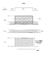
しかしこの比較例の場合には、図5に示すように、ゲートソース間電圧VgsLの正バイアス電圧もまたソース電極42に付加されるソース電圧-VsL分、つまり負バイアス電圧-Vzd分だけオフセットされる。このため、ゲートソース間電圧VgsLの正バイアス電圧をゲート閾値電圧Vthより十分高く確保(この例では+10Vを確保)するためには、制御端子62からゲート電極43に対して出力するゲート電圧VgLを負バイアス電圧-Vzdのオフセット分(-5V分)だけ高く供給する必要がある。このため、その高いゲート電圧VgL(+15V)を出力できる分だけ供給電圧(+Vcc)の高いドライブ用電源を用意する必要があり、全体の回路規模を大型化してしまう。
<第1実施形態のゲートドライブ回路>
以上に対して、本実施形態が備えるゲートドライブ回路22では、ゲート電圧Vgに応じてゲートソース間電圧Vgsに対する負バイアス電圧-Vzdの付加を切り替える。このような動作を実現する本実施形態のゲートドライブ回路22の回路構成を図6に示す。
以上に対して、本実施形態が備えるゲートドライブ回路22では、ゲート電圧Vgに応じてゲートソース間電圧Vgsに対する負バイアス電圧-Vzdの付加を切り替える。このような動作を実現する本実施形態のゲートドライブ回路22の回路構成を図6に示す。
上記図3に示した比較例のゲートドライブ回路22Eとの差異点としては、図6に示す本実施形態のゲートドライブ回路22がさらにツェナーダイオードZDの両端子間の短絡または遮断を制御するよう設けられた第1補助スイッチング素子Q1(第1補助素子に相当)と、並列線73の導通または遮断を制御するよう設けられた第2補助スイッチング素子Q2(第2補助素子に相当)とを有している点にある。また、これら2つの補助スイッチング素子Q1,Q2の各ゲート電極(第1補助ゲート電極、第2補助ゲート電極に相当)は、スルーレート(dV/dt)調整用の共通の第2ゲート抵抗Rg2を介して制御線51に接続されている。そして本実施形態では、接続線71、電極線52、制限抵抗Rzd、ツェナーダイオードZD、並列線73、負バイアス用コンデンサC1、第1補助スイッチング素子Q1、第2補助スイッチング素子Q2、及び第2ゲート抵抗Rg2が負バイアス回路部54を構成する。なお、この負バイアス回路部54が、各請求項記載の負バイアス電位の付加と無付加を切り替えるように構成された手段に相当する。
第1補助スイッチング素子Q1は、例えばNチャンネル型MOSで構成したノーマリオフタイプの半導体スイッチング素子であり、上記ゲート電圧Vg(ゲート制御信号に相当)がハイレベルである場合、つまり制御線51に給電電位+Vccの電位(所定の正電位に相当)が付加された場合にツェナーダイオードZDの両端子間を短絡する。また第2補助スイッチング素子Q2は、例えばPチャンネル型MOSで構成したノーマリオンタイプの半導体スイッチング素子であり、上記ゲート電圧Vgがハイレベルである場合に並列線73を遮断する。
以上のように構成された本実施形態のゲートドライブ回路22では、切替制御信号SがON出力された場合、図7に示すような状態となる。なお、ここでは負バイアス用コンデンサC1があらかじめ充電されているとする(この初期充電のシーケンスについては後に詳述する)。また図中においては、各補助スイッチング素子Q1,Q2を簡略化してそれらのON/OFF状態が明確になるよう示している。図7において、切替制御信号SがON出力されていることによりドライブIC53(ゲート制御部)の制御端子62には給電電位+Vccが付加され、下アームスイッチング素子QLのゲート電極43にはハイレベルのゲート電圧Vgが付加される。一方、ゲート電圧Vgがハイレベルであることで、第1補助スイッチング素子Q1が導通してツェナーダイオードZDの両端子間を短絡するとともに、第2補助スイッチング素子Q2が並列線73を遮断して負バイアス用コンデンサC1の放電を防ぐ。これにより、接続点72における電位がGND接地電位(略0電位に相当)となり、下アームスイッチング素子QLのソース電極42には略0電位が付加される。以上により、切替制御信号SがON出力された場合には、下アームスイッチング素子QLのゲートソース間電圧Vgsに正バイアス電圧(+Vcc)が付加され、当該下アームスイッチング素子QLがON状態となる。
また、切替制御信号SがOFF出力された場合、図8に示すような状態となる。すなわち、切替制御信号SがOFF出力されていることによりドライブIC53の制御端子62は略0電位となり、下アームスイッチング素子QLのゲート電圧Vgはローレベル(略0電位に相当)となる。一方、ゲート電圧Vgがローレベルであることで、第1補助スイッチング素子Q1が遮断してツェナーダイオードZDを有効に機能させるとともに、第2補助スイッチング素子Q2が並列線73を導通して負バイアス用コンデンサC1をツェナーダイオードZDに並列接続させる。これにより、接続点72における電位が負バイアス用コンデンサC1の充電電位(Vzd:所定の電位差に相当)となり、これに相当する負バイアス電位が下アームスイッチング素子QLのソース電極42に付加される。以上により、切替制御信号SがOFF出力された場合には、下アームスイッチング素子QLのゲートソース間電圧Vgsに負バイアス電圧(-Vzd)が付加され、当該下アームスイッチング素子QLがOFF状態となる。
以上のように作動する本実施形態のゲートドライブ回路22の場合の各種切替状態及びゲートソース間電圧VgsLのタイムチャートを、図9に示す。この図9においては、第1補助スイッチング素子Q1と第2補助スイッチング素子Q2のそれぞれの切替状態(ON/OFF)も併せて示しており、第1補助スイッチング素子Q1の挙動波形は切替制御信号SLとほぼ同じとなり、第2補助スイッチング素子Q2の挙動波形は切替制御信号SL及び第1補助スイッチング素子Q1とほぼ逆位相となる。それ以外は、上記図4に示したタイムチャートと同じ挙動波形となっており、すなわち本実施形態のゲートドライブ回路22においても上記比較例と同等に負バイアス電圧によってセルフターンオン電位Aを相殺し、セルフターンオンを防止できる。
しかし本実施形態のゲートドライブ回路22の場合は、上記図5に対応する図10に示すように、切替制御信号SLがOFF出力されている間だけ、すなわちゲート電圧VgLがローレベルである間だけソース電極42に負バイアス電位が付加され、ゲートソース間電圧VgsLが負バイアス電圧-Vzd分だけオフセットされる。また、切替制御信号SLがON出力されている間、すなわちゲート電圧VgLがハイレベルである間は、ソース電極42は略0電位となりゲートソース間電圧VgsLはオフセットされない。このため、切替制御信号SLがON出力されている間に制御端子62から正バイアス電圧分のゲート電圧VgL(この例では+10V)を出力するだけで、ゲートソース間電圧VgsLの正バイアス電圧をゲート閾値電圧Vthより十分高く確保(この例では+10Vを確保)できる。すなわち本実施形態では、ゲート電圧VgLに応じてソース電極42に対しGND接地電位(略0電位)と負バイアス電位(-Vzd)を切り替えて付加することで、上記比較例の場合よりもドライブ用電源の必要供給電圧(+Vcc)を抑えることができ、全体の回路規模を省力化できる。
なお、本実施形態では下アームスイッチング素子QLにノーマリオフタイプの半導体スイッチング素子32を適用した場合を例に説明したが、これに限られず、下アームスイッチング素子QLにノーマリオンタイプの半導体スイッチング素子32を適用してもよい。この場合には、第1補助スイッチング素子Q1をノーマリオンタイプとし、第2補助スイッチング素子Q2をノーマリオフタイプとすることで、上記実施形態と同等の機能が得られる(特に図示せず)。なおこの場合には、切替制御信号SLをON出力した際には下アームスイッチング素子QLがOFF状態となり、切替制御信号SLをOFF出力した際には下アームスイッチング素子QLがON状態となる。
<負バイアス用コンデンサの初期充電シーケンス>
以下において、モータ制御装置100における負バイアス用コンデンサC1の初期充電シーケンスについて説明する。まず、本実施形態の例のようにノーマリオフタイプの下アームスイッチング素子QLを制御するゲートドライブ回路22だけを見れば、切替制御信号SLをOFF出力することで第2補助スイッチング素子Q2をON状態とし、並列線73を導通させて負バイアス用コンデンサC1を充電できる(上記図8参照)。しかし、上述したように下アームスイッチング素子QLにノーマリオンタイプの半導体スイッチング素子32を適用した場合には、切替制御信号SLをON出力した際に負バイアス用コンデンサC1を充電できる(図示省略)。また上述したように、インバータ5のブリッジ回路21では直流母線4間の縦短絡を防ぐために、直列に接続する上下2つのアームスイッチング素子QH,QLを同時にON状態にすることはできない。
以下において、モータ制御装置100における負バイアス用コンデンサC1の初期充電シーケンスについて説明する。まず、本実施形態の例のようにノーマリオフタイプの下アームスイッチング素子QLを制御するゲートドライブ回路22だけを見れば、切替制御信号SLをOFF出力することで第2補助スイッチング素子Q2をON状態とし、並列線73を導通させて負バイアス用コンデンサC1を充電できる(上記図8参照)。しかし、上述したように下アームスイッチング素子QLにノーマリオンタイプの半導体スイッチング素子32を適用した場合には、切替制御信号SLをON出力した際に負バイアス用コンデンサC1を充電できる(図示省略)。また上述したように、インバータ5のブリッジ回路21では直流母線4間の縦短絡を防ぐために、直列に接続する上下2つのアームスイッチング素子QH,QLを同時にON状態にすることはできない。
そこで、モータ3を駆動する前の準備シーケンスとして、まずブリッジ回路21が備える6つのアームスイッチング素子QH,QLのうち各相の上アームスイッチング素子QHを全てOFF状態とすることで、直流母線4間の縦短絡とモータ3への給電を阻止する。その間に、各下アームスイッチング素子QLに対してPWM制御の作動に準じたON/OFFの切り替えを複数回繰り返して行うことで、各アームスイッチング素子QH,QLがノーマリオフ、ノーマリオンのいずれのタイプであっても同等に負バイアス用コンデンサC1を充電できる。そして下段側の充電完了後に各相の下アームスイッチング素子QLを全てOFF状態とし、その間に各上アームスイッチング素子QHに対してPWM制御の作動に準じたON/OFFの切り替えを複数回繰り返して上段側の充電を行えばよい。
なお、上記の初期充電シーケンスにおいて、各ゲートドライブ回路22に対し切替制御信号SLのON/OFFを繰り返す際の必要スイッチング回数Nについては、以下のように求められる。
N=a・f・Rzd・C1 ・・・(1)
ただし、aは係数、fはPWM制御のキャリア周波数、Rzdは制限抵抗Rzdの抵抗値、C1は負バイアスコンデンサC1の容量である。なお、Rzd・C1の値は、負バイアス用コンデンサC1がツェナーダイオードZDの降伏電圧Vzdの約63%に達するまでの時定数に相当する。
N=a・f・Rzd・C1 ・・・(1)
ただし、aは係数、fはPWM制御のキャリア周波数、Rzdは制限抵抗Rzdの抵抗値、C1は負バイアスコンデンサC1の容量である。なお、Rzd・C1の値は、負バイアス用コンデンサC1がツェナーダイオードZDの降伏電圧Vzdの約63%に達するまでの時定数に相当する。
ここで、切替制御信号Sのデューティ比が平均50%であるとした場合、負バイアス用コンデンサC1の両端子間電圧をツェナーダイオードZDの降伏電圧Vzdと同等にするには、係数aの値を2以上に設定するのが望ましいと考えられる。例えば、f=50kHz、Rzd=1.5kΩ、C1=1μHとした場合、上記(1)式から、
N=2×50000×1500×0.000001=150
となり、150回程度という現実的な回数でスイッチングを繰り返すことで負バイアス用コンデンサC1の両端子間電圧をツェナーダイオードZDの降伏電圧Vzdと同等に充電できる。実際の設計では、最終的にC1の両端子間電圧を実測して適正な係数aを設定すればよい。なお、同じ下段側において各アームスイッチング素子QLのスイッチングを同時に行ってもよいし、個別に行ってもよい。また、上段側を先に充電した後に下段側を充電してもよい。
N=2×50000×1500×0.000001=150
となり、150回程度という現実的な回数でスイッチングを繰り返すことで負バイアス用コンデンサC1の両端子間電圧をツェナーダイオードZDの降伏電圧Vzdと同等に充電できる。実際の設計では、最終的にC1の両端子間電圧を実測して適正な係数aを設定すればよい。なお、同じ下段側において各アームスイッチング素子QLのスイッチングを同時に行ってもよいし、個別に行ってもよい。また、上段側を先に充電した後に下段側を充電してもよい。
<本実施形態の効果>
以上説明したように、本実施形態のゲートドライブ回路22、インバータ5、及びモータ制御装置100によれば、ゲート電圧VgLの電位に応じて、下アームスイッチング素子QLのソース電極42に対しGND接地電位(略0電位)と負バイアス電位(-Vzd)を切り替えて付加するように構成された負バイアス回路部54を備えている。これにより、ソース電極42にはゲート電圧VgLの電位に応じて必要時にだけ負バイアス電位を付加し、それ以外では略0電位にできる。すなわち当該下アームスイッチング素子QLをOFF状態としてセルフターンオン現象を防ぐ際には、ソース電極42に負バイアス電位を付加すればよい。またその一方で、当該下アームスイッチング素子QLを導通状態とする際には、ソース電極42を略0電位とすることで、ゲート電圧VgLはゲート閾値電圧Vthを超えるだけの電位で出力するだけでゲートソース間電圧VgsLの正バイアス電圧を十分確保でき、つまりドライブ用電源の供給電圧(+Vcc)を低減できる。この結果、ゲートドライブ回路22全体、ひいてはモータ制御装置100全体の回路規模の省力化が可能となる。
以上説明したように、本実施形態のゲートドライブ回路22、インバータ5、及びモータ制御装置100によれば、ゲート電圧VgLの電位に応じて、下アームスイッチング素子QLのソース電極42に対しGND接地電位(略0電位)と負バイアス電位(-Vzd)を切り替えて付加するように構成された負バイアス回路部54を備えている。これにより、ソース電極42にはゲート電圧VgLの電位に応じて必要時にだけ負バイアス電位を付加し、それ以外では略0電位にできる。すなわち当該下アームスイッチング素子QLをOFF状態としてセルフターンオン現象を防ぐ際には、ソース電極42に負バイアス電位を付加すればよい。またその一方で、当該下アームスイッチング素子QLを導通状態とする際には、ソース電極42を略0電位とすることで、ゲート電圧VgLはゲート閾値電圧Vthを超えるだけの電位で出力するだけでゲートソース間電圧VgsLの正バイアス電圧を十分確保でき、つまりドライブ用電源の供給電圧(+Vcc)を低減できる。この結果、ゲートドライブ回路22全体、ひいてはモータ制御装置100全体の回路規模の省力化が可能となる。
また、本実施形態によれば、下アームスイッチング素子QLがいわゆるノーマリオフタイプである場合、ON状態とする際にはゲート電圧VgLをハイレベル(所定の正電位)とする。また、OFF状態とする際には、ゲート電圧VgLをローレベル(略0電位)とする。これに対応して、負バイアス回路部54は、下アームスイッチング素子QLがON状態である際、つまりゲート電圧VgLがハイレベルである際にソース電極42に対して略0電位を付加する。これにより、ゲート電圧VgLはゲート閾値電圧Vthを超えるだけの電位で出力するだけでゲートソース間電圧VgsLの正バイアス電圧を十分確保でき、つまりドライブ用電源の供給電圧を低減できる。また、負バイアス回路部54は、下アームスイッチング素子QLが遮断状態である際、つまりゲート電圧VgLがローレベルである際にゲート電極43の略0電位に対してソース電極42の電位がセルフターンオン電位Aを超える電位差で高くなるよう負バイアス電位(+Vzd)を付加する。これにより、上記ミラー効果によってゲート電極43に付加されるセルフターンオン電位Aを相殺してセルフターンオン現象を防ぐことができる。以上のように作動することで、本実施形態のゲートドライブ回路22をノーマリオフタイプの下アームスイッチング素子QLの制御に適用できる。
なお、本実施形態では下アームスイッチング素子QLに対応したゲートドライブ回路22について説明したが、本発明はこれに限られない。例えば、デットタイムDT後に上アームスイッチング素子QHをOFF状態としたまま下アームスイッチング素子QLをON状態にターンオンした場合でも、上アームスイッチング素子QHにおいてミラー効果によるセルフターンオン現象が発生する。このため、上アームスイッチング素子QHに対しても本実施形態のゲートドライブ回路22を適用することは有効である。また、各アームスイッチング素子QH,QLがノーマリオンタイプである場合でも、第1補助スイッチング素子Q1をノーマリオンタイプとし、第2補助スイッチング素子Q2をノーマリオフタイプとすることで、本実施形態のゲートドライブ回路22を適用できる。
また、本実施形態によれば、負バイアス回路部54は、ゲート電圧Vgがハイレベルである際にドライブ用電源から充電した充電電位を、ゲート電圧Vgがローレベルである際に負バイアス電位としてソース電極42に付加する。これにより、ドライブ用電源と独立した個別の電源を用意せずとも、負バイアス回路部54がその必要時に負バイアス電位を生成してソース電極42に付加できるため、回路構成を簡略化できる。
また、本実施形態によれば、ドライブIC53は、ドライブ用電源からの給電正電位(+Vcc)を出力する給電端子61と、制御線51を介してゲート電極43に接続されてゲート電圧Vgを給電正電位のハイレベルと略0電位のローレベルに切り替えて出力する制御端子62と、略0電位のGND接地電位を保持する接地端子63と、を有し、負バイアス回路部54は、給電端子61と接地端子63を接続する接続線71と、接続線71上の接続点72にソース電極42を接続する電極線52と、接続線71上で接続点72より接地端子63側に配置され、接地端子63から給電端子61へ向かう方向を順方向として所定の降伏電圧(Vzd)を有するツェナーダイオードZDと、ツェナーダイオードZDの両端子間を接続する並列線73上に配置された負バイアス用コンデンサC1と、ツェナーダイオードZDの両端子間の短絡または遮断を制御するように構成された第1補助スイッチング素子Q1と、を有する。このような回路構成とすることにより、ツェナーダイオードZDと負バイアス用コンデンサC1の並列回路が負バイアス電位を生成保持し、第1補助スイッチング素子Q1がソース電極42に対してその負バイアス電位の付加と無付加(接地)を切り替える動作を実現できる。
また、本実施形態によれば、負バイアス回路部54が、並列線73の導通または遮断を制御するように構成された第2補助スイッチング素子Q2を有することにより、負バイアス電位として生成される負バイアス用コンデンサC1の充電電位を不必要に放電することを防ぐことができる。
また、本実施形態によれば、第1補助スイッチング素子Q1がノーマリオフタイプの半導体スイッチング素子であり、第2補助スイッチング素子Q2がノーマリオンタイプの半導体スイッチング素子であり、各補助スイッチング素子Q1,Q2のゲート電極が制御線51に接続されている。このように構成することで、下アームスイッチング素子QLがノーマリオフタイプであってON状態にある際、つまりゲート電圧VgLがハイレベルである際には、第1補助スイッチング素子Q1が導通してツェナーダイオードZDを短絡させ、ソース電極42を接地させることができる。またこのとき第2補助スイッチング素子Q2は、並列線73を遮断して負バイアス用コンデンサC1の充電電位の放電を防ぐことができる。一方、下アームスイッチング素子QLがOFF状態である際、つまりゲート電圧Vgがローレベルである際には、第1補助スイッチング素子Q1が遮断してツェナーダイオードZDと負バイアス用コンデンサC1の並列回路における充電電位をソース電極42に負バイアス電位として付加できる。またこのとき第2補助スイッチング素子Q2は、並列線73を導通させて負バイアス用コンデンサC1の充電と充電電位の付加を可能にする。よって、本実施形態における上記動作を具体的に実現できる。
<第2実施形態>
以下、第2の実施の形態について図面を参照しつつ説明する。
以下、第2の実施の形態について図面を参照しつつ説明する。
まず、図11を用いて、第2実施形態に係るモータ制御装置100A全体の回路構成について説明する。この図11において、上記図1に示したモータ制御装置100との差異点としては、インバータ5Aのブリッジ回路21Aが備える全てのアームスイッチング素子QH,QLがフライホイールダイオード33を設けずに半導体スイッチング素子32だけで構成している点にある。例えば特性のよくない寄生ダイオード34を備えるGaN-FETで構成する半導体スイッチング素子32を用いた場合、フライホイールダイオード33を設けると特に実装面積が増大してしまう。このような場合に、インバータ5A、特にブリッジ回路21Aにおいては、周波数特性の向上を目的とした小型高密度での実装を図るためこのようにフライホイールダイオード33を省略した構成が取られる。
<フライホイールダイオードの設置を省略した場合の問題点について>
しかし、このようにフライホイールダイオード33の設置を省略した場合には、図12に示すような還流電流の発生時に消費電力で以下のような問題が生じる。すなわち、モータ3の回転駆動中で少なくとも同じ組(同じ相)の上下2つのアームスイッチング素子QH,QLが同時にOFF状態となっている間、つまり上述したデッドタイム期間DT中においては、モータ3のコイルにおけるインダクタンスの作用で直流母線4のN線からP線へ向けて回生電流を半導体スイッチング素子32の逆方向(つまりソース電極42からドレイン電極41へ向かう方向)に流そうとする還流作用が生じる。なお、図12においては、図示の煩雑を回避するために、2相分のアームスイッチング素子QH,QLだけを図示している。
しかし、このようにフライホイールダイオード33の設置を省略した場合には、図12に示すような還流電流の発生時に消費電力で以下のような問題が生じる。すなわち、モータ3の回転駆動中で少なくとも同じ組(同じ相)の上下2つのアームスイッチング素子QH,QLが同時にOFF状態となっている間、つまり上述したデッドタイム期間DT中においては、モータ3のコイルにおけるインダクタンスの作用で直流母線4のN線からP線へ向けて回生電流を半導体スイッチング素子32の逆方向(つまりソース電極42からドレイン電極41へ向かう方向)に流そうとする還流作用が生じる。なお、図12においては、図示の煩雑を回避するために、2相分のアームスイッチング素子QH,QLだけを図示している。
このような還流期間(デッドタイム期間DT)において、各アームスイッチング素子QH,QLにフライホイールダイオード33を設けている場合には、それを介して還流電流を円滑に流すことができる。しかし、上記図11に示した第2実施形態のように、各アームスイッチング素子QH,QLでフライホイールダイオード33の設置を省略した場合、還流電流は半導体スイッチング素子32自体に潜在的に備えられている寄生ダイオード34を介して流すことになる。
図示するように半導体スイッチング素子32が潜在的に備える寄生ダイオード34は、ソース電極42からドレイン電極41へ向かう方向を順方向とし、当該半導体スイッチング素子32を構成する素材や内部の回路構成によって特性が大きく相違する。ここで例えば、図13は一般的なIGBTの半導体スイッチング素子32に逆並列で接続されるフライホイールダイオード33(通常のダイオードと同等)の電圧電流特性を示しているが、図示するように通常のダイオードであってもその順方向に対してある一定の順方向電圧Vfを超える電圧を付加しない限り順方向電流が流れない。なお、ここでは順方向電圧領域だけに着目し、逆方向電圧領域におけるリーク電流とブレークダウン現象については無視する。このような通常のダイオードの場合においては、電圧の変化割合ΔVに対する電流の変化割合ΔIの比の逆数ΔV/ΔIが抵抗値Rに相当し、順方向通電状態における消費電力がP=Vf・I+I2・ΔV/ΔIとなる。
これに対し、例えば特性のよくない寄生ダイオード34を備えるGaN-FETで構成する半導体スイッチング素子32(フライホイールダイオード33非設置)の電圧電流特性は図14に示すようになる。この図14において、ゲートソース間電圧Vgsに負バイアス電圧が付加された遮断状態(Vgs<0)では、ソースドレイン間電圧Vsdに逆方向電圧(Vsd<0)を付加した場合にだけ逆方向電流(Ids<0)が流れ、つまり寄生ダイオード34を介してソース電極42からドレイン電極41へ向かう方向に電流が流れる(図中の左下の領域参照)。しかしこの逆方向電流の特性においては、ゲートソース間電圧Vgsに付加された負バイアス電圧の大きさに比例して、当該寄生ダイオード34における上述の順方向電圧Vf(この場合、逆方向電流を流すために最低限必要な逆方向ソースドレイン間電圧Vsd)が増大してしまう。
このように特性のよくない寄生ダイオード34を潜在的に備える半導体スイッチング素子32では、負バイアス電圧を付加した状態で回生電流を還流した際に、当該半導体スイッチング素子32内において軽視できないほどの大きな導通損失(導通時における消費電力)が発生してしまう。つまり、上記図9に対応する図15に示すように、上アームスイッチング素子QHと下アームスイッチング素子QLの両方がOFF状態となるデッドタイム期間DTにおいては、逆方向電流である還流電流Idsが流れる。また同時に、当該デッドタイム期間DT中においては、ソースドレイン間電圧Vdsとして負バイアス電圧に比例した大きさで寄生ダイオード34の順方向電圧Vf分の逆方向電位差(-Vfv)が生じる。このため、デッドタイム期間DT中には、ゲートソース間電圧Vgsに付加される負バイアス電圧に比例した大きな通電損失P=Ids・(Vds+Vgs)(以下、デッドタイムロスPという)が生じてしまう。
<第2実施形態のゲートドライブ回路>
以上に対して、第2実施形態のゲートドライブ回路22Aでは、図16に示す回路構成の負バイアス回路部54Aを備えることで上記デッドタイムロスの低減を図る。上記図6に示した第1実施形態の負バイアス回路部54との差異点としては、図16に示す第2実施形態の負バイアス回路部54Aがさらに制御線51を接地する接地線74と、接地線74上に直列に配置された時定数抵抗R2(第1抵抗)及び時定数コンデンサC3(第2コンデンサ)と、を有し、2つの補助スイッチング素子Q1,Q2の各ゲート電極が、共通の第2ゲート抵抗Rg2を介して時定数抵抗Rと時定数コンデンサCの間で接地線74に接続し、さらに接地線74上の時定数抵抗R2を介して制御線51に接続している点で相違している。その他の部分については上記第1実施形態と同じであり、説明を省略する。
以上に対して、第2実施形態のゲートドライブ回路22Aでは、図16に示す回路構成の負バイアス回路部54Aを備えることで上記デッドタイムロスの低減を図る。上記図6に示した第1実施形態の負バイアス回路部54との差異点としては、図16に示す第2実施形態の負バイアス回路部54Aがさらに制御線51を接地する接地線74と、接地線74上に直列に配置された時定数抵抗R2(第1抵抗)及び時定数コンデンサC3(第2コンデンサ)と、を有し、2つの補助スイッチング素子Q1,Q2の各ゲート電極が、共通の第2ゲート抵抗Rg2を介して時定数抵抗Rと時定数コンデンサCの間で接地線74に接続し、さらに接地線74上の時定数抵抗R2を介して制御線51に接続している点で相違している。その他の部分については上記第1実施形態と同じであり、説明を省略する。
以上のように構成された第2実施形態のゲートドライブ回路22Aでは、1動作周期中(PWM制御の1キャリア周期中)に4つ工程I~IVを経て状態が切り替わる。まず、切替制御信号SがON出力されている際には、図17に示すような第1工程Iの状態となる。なお、この場合でも負バイアス用コンデンサC1と時定数コンデンサC3があらかじめ初期充電シーケンスにより充電済みであるとする。
図17に示す第1工程Iにおいて、切替制御信号SがON出力されていることによりドライブIC53の制御端子62には給電電位+Vccが付加され、下アームスイッチング素子QLのゲート電極43にはハイレベルのゲート電圧Vgが付加される。一方、ゲート電圧Vgがハイレベルであるとともに時定数コンデンサC3が充電状態であることで、第1補助スイッチング素子Q1が導通してツェナーダイオードZDの両端子間を短絡し、また第2補助スイッチング素子Q2が並列線73を遮断して負バイアス用コンデンサC1の放電を防ぐ。これにより、接続点72における電位がGND接地電位となり、下アームスイッチング素子QLのソース電極42には略0電位が付加される。以上により、切替制御信号SがON出力されているこの第1工程Iでは、下アームスイッチング素子QLのゲートソース間電圧Vgsに正バイアス電圧(+Vcc)が付加され、当該下アームスイッチング素子QLがON状態となる(上記図7の状態と同等)。
次に、切替制御信号SがOFF出力に切り替えた場合、その初期時には図18に示すような第2工程IIの状態となる。すなわち、切替制御信号SがOFF出力されていることによりドライブIC53の制御端子62は略0電位となり、下アームスイッチング素子QLのゲート電圧Vgはローレベルとなる。一方、ゲート電圧Vgがローレベルであるものの、時定数コンデンサC3が充電状態であることで各補助スイッチング素子Q1,Q2のゲート電極電位はハイレベルを維持しており、上記第1工程Iに引き続きこの第2工程IIにおいても第1補助スイッチング素子Q1の導通状態と第2補助スイッチング素子Q2の遮断状態が維持される。つまり、ツェナーダイオードZDにおける両端子間の短絡状態と、負バイアス用コンデンサC1の充電保持状態が維持される。以上により、切替制御信号SをOFF出力に切り替えた直後の第2工程IIでは、下アームスイッチング素子QLのゲートソース間電圧Vgsに略0バイアス電圧(つまり略0電圧)が付加され、当該下アームスイッチング素子QLがOFF状態となる。
しかし、その後に時定数コンデンサC3の放電が進んだ際には、図19に示すような第3工程IIIの状態となる。すなわち、時定数コンデンサC3の放電が進むことにより各補助スイッチング素子Q1,Q2のゲート電位もまたゲート電圧Vgと同様のローレベルとなることで、第1補助スイッチング素子Q1が遮断状態に切り替わり、第2補助スイッチング素子Q2が導通状態に切り替わる。つまり、ツェナーダイオードZDと負バイアス用コンデンサC1の並列回路が有効に機能して接続点72における電位が負バイアス用コンデンサC1の充電電位(Vzd)となり、これに相当する負バイアス電位が下アームスイッチング素子QLのソース電極42に付加される。以上により、切替制御信号SをOFF出力に切り替えた後の安定期である第3工程IIIでは、下アームスイッチング素子QLのゲートソース間電圧Vgsに負バイアス電圧(-Vzd)が付加され、当該下アームスイッチング素子QLがOFF状態となる(上記図8の状態と同等)。なお、上記第2工程IIから第3工程IIIへ切り替わるタイミングは、時定数抵抗R2と時定数コンデンサC3で決まる時定数を調整することで任意に設定できる。
次に、切替制御信号SをON出力に切り替えた場合、その初期時には図20に示すような第4工程IVの状態となる。すなわち、切替制御信号SがON出力されていることによりドライブIC53の制御端子62には給電電位+Vccが付加され、下アームスイッチング素子QLのゲート電極43にはハイレベルのゲート電圧Vgが付加される。一方、ゲート電圧Vgがハイレベルであるものの、上記第3工程III中に放電された時定数コンデンサC3がまだ十分に充電していない間は各補助スイッチング素子Q1,Q2のゲート電極電位がローレベルを維持しており、上記第3工程IIIに引き続きこの第4工程IVにおいても第1補助スイッチング素子Q1の遮断状態と第2補助スイッチング素子Q2の導通状態が維持される。つまり、負バイアス用コンデンサC1の充電電位(Vzd)に相当する負バイアス電位が下アームスイッチング素子QLのソース電極42に付加される。以上により、切替制御信号SをON出力に切り替えた直後の第4工程IVでは、下アームスイッチング素子QLのゲートソース間電圧Vgsに正バイアス電圧と負バイアス電圧の差分電圧(+Vcc-Vzd)が付加される。給電電位+Vccの絶対値が、負バイアス用コンデンサC1の充電電位Vzdの絶対値よりも十分大きく確保できていれば、結果的にゲートソース間電圧Vgsにゲート閾値電圧Vthを超える正バイアス電圧を付加することができ、当該下アームスイッチング素子QLがON状態となる。なお、この第4工程IVは、時定数コンデンサC3が十分に充電した際に上記第1工程Iに移行するため、比較的短い期間の工程となる。
以上のような工程I~IVを経て作動する第2実施形態のゲートドライブ回路22Aの場合の各種切替状態及びゲートソース間電圧VgsLのタイムチャートを、図21に示す。上記図9に対応するこの図21においては、制御切替信号SLがOFF出力されてゲート電極43の電位がローレベルとなった後でも、時定数抵抗R2と時定数コンデンサC3で決まる時定数期間LT(所定時間に相当)の間だけソース電極42の電位Vsが略0電位に維持されてゲートソース間電圧VgsLには略0電圧が付加される(負バイアス電圧が無付加;第2工程II)。その後に時定数期間LTが経過した時点では、時定数コンデンサC3が放電状態となって2つの補助スイッチング素子Q1,Q2のON/OFF状態が切り替わることにより、ソース電極42の電位Vsがゲート電極43の電位Vgより高くなり、すなわちゲートソース間電圧VgsLには-Vzd(この例の-5V)の負バイアス電圧が付加される(第3工程III)。この状態では、セルフターンオン電位Aが負バイアス電圧-Vzdに相殺され、上記第1実施形態と同様に下アームスイッチング素子QLにおけるセルフターンオン現象を防ぐことができる。
そして図示するように、上記時定数期間LTをデッドタイムDTとほぼ同じ期間に設定してセルフターンオン電位Aの発生前に第2工程IIから第3工程IIIに移行することで、少なくともその時定数期間LTと同等のデッドタイムDT中においては、ゲートソース間電圧VgsLに付加される負バイアス電圧を略0電圧にできる。すなわち、当該下アームスイッチング素子QLが備える寄生ダイオード34の順方向電圧Vfを小さく抑えることができ(上記図14参照)、またソースドレイン間電圧Vdsも同等に低減できる。このため、同じデッドタイムDT中に大きな還流電流Idsが流れても(上記図15参照)、その間のデッドタイムロスP=Ids・(Vsd+Vgs)を低減できる。
<第2実施形態の効果>
以上説明したように、第2実施形態のゲートドライブ回路22A、インバータ5A、及びモータ制御装置100Aによれば、負バイアス回路部54Aが、ゲート電圧Vgがローレベルとなってから時定数期間LT経過後にゲートソース間電圧Vgsに負バイアス電位を付加する。これにより、半導体スイッチング素子QLがOFF状態となってから時定数期間LTが経過するまでの間は当該半導体スイッチング素子QLに負バイアス電圧が付加されずに寄生ダイオード34の順方向電圧Vfの増加を抑えてデッドタイムロスPを低減できる。以上により第2実施形態では、デッドタイムロスPを低減しつつ、上述したドライブ用電源の省力化と併せてブリッジ回路21Aにおけるフライホイールダイオード33の設置を省略した小型高密度での実装を可能とし、ゲートドライブ回路22A全体の回路規模の省力化を実現できる。
以上説明したように、第2実施形態のゲートドライブ回路22A、インバータ5A、及びモータ制御装置100Aによれば、負バイアス回路部54Aが、ゲート電圧Vgがローレベルとなってから時定数期間LT経過後にゲートソース間電圧Vgsに負バイアス電位を付加する。これにより、半導体スイッチング素子QLがOFF状態となってから時定数期間LTが経過するまでの間は当該半導体スイッチング素子QLに負バイアス電圧が付加されずに寄生ダイオード34の順方向電圧Vfの増加を抑えてデッドタイムロスPを低減できる。以上により第2実施形態では、デッドタイムロスPを低減しつつ、上述したドライブ用電源の省力化と併せてブリッジ回路21Aにおけるフライホイールダイオード33の設置を省略した小型高密度での実装を可能とし、ゲートドライブ回路22A全体の回路規模の省力化を実現できる。
また、本実施形態によれば、上記時定数期間LTは、ゲート電圧Vgがローレベルとなってからゲート電極43にミラー効果によるセルフターンオン電位Aが付加されるまでの所要時間以内に設定されている。これにより、セルフターンオン現象の発生前に負バイアス電圧を付加できるため、上記デッドタイムロスPの低減とセルフターンオン現象の防止を両立できる。
また、本実施形態によれば、負バイアス回路部54Aは、制御線51を接地する接地線74と、接地線74上に直列に配置された時定数抵抗R2及び時定数コンデンサC3と、を有し、2つの補助スイッチング素子Q1,Q2の各ゲート電極は、時定数抵抗R2と時定数コンデンサC3の間で接地線74に接続し、当該接地線74を介して制御線51に接続している。このような回路構成とすることにより、時定数抵抗R2と時定数コンデンサC3の時定数を調整することで、上記時定数期間LTを任意に設定することができる。
なお、上記第2実施形態は、上記図14に示したような特性のよくない寄生ダイオード34を備えるGaN-FET(ノーマリオン)を半導体スイッチング素子32として用いた場合にデッドタイムロスPを低減できる構成として有用であるが、これに限られない。他にも、特性が良好な寄生ダイオード34を備えるSi-MOSFET、SiC-MOSFET,及びGaN-HEMTを半導体スイッチング素子32として用いた場合であっても、上記第2実施形態を適用してもよい。また、寄生ダイオード34を備えずにフライホイールダイオード33の設置が不可欠なSi-IGBTやSiC-IGBTに対しても、フライホイールダイオード33を設置した上で、負バイアス回路部54Aを含めた上記第2実施形態を適用してもよい。
なお、開示の実施形態は、上記に限られるものではなく、その趣旨及び技術的思想を逸脱しない範囲内で種々の変形が可能である。以下、そのような変形例を説明する。
<半導体スイッチング素子のゲート構造が電流型である場合>
例えば、GaN-GITのようにゲート構造がトランジスタと同様の電流型である半導体スイッチング素子32をアームスイッチング素子QH,QLに用いた場合には、ゲート電極43の導通抵抗が増加して電力損失(スイッチング損失)が増大しやすい。これに対しては、図22に示すような回路構成のゲートドライブ回路22Bを適用することで解決できる。
例えば、GaN-GITのようにゲート構造がトランジスタと同様の電流型である半導体スイッチング素子32をアームスイッチング素子QH,QLに用いた場合には、ゲート電極43の導通抵抗が増加して電力損失(スイッチング損失)が増大しやすい。これに対しては、図22に示すような回路構成のゲートドライブ回路22Bを適用することで解決できる。
つまり、図22に示す本変形例のゲートドライブ回路22Bでは、上記図16に示した第2実施形態のゲートドライブ回路22Aと比較して、第3ゲート抵抗Rg3とゲートコンデンサC4の直列回路を第1ゲート抵抗Rg1に対して並列に接続し、第3ゲート抵抗Rg3とゲートコンデンサC4の中間点を第4ゲート抵抗Rg4を介してドライブIC53Bの排電端子65に接続している点で相違している。また、ドライブIC53Bの排電端子65は、切替制御信号SがOFF出力された場合に接地するよう構成されている。
このようなゲートドライブ回路22Bの構成とすることで、切替制御信号SがON出力された場合には制御端子62からのゲート電圧Vgがハイレベルになるとともに低インピーダンスのゲートコンデンサC4を通して下アームスイッチング素子QLのゲート電極43の電位がチャージされ、下アームスイッチング素子QLをすぐにON状態に切り替えることができる。その後、第1ゲート抵抗Rg1を介してゲート電極43に継続的に電流を流して当該ゲート電極43の低導通抵抗を維持できる。つまり、半導体スイッチング素子32のターンオン動作を早めることができ、スイッチング損失を低減できる。
また、切替制御信号SがOFF出力に切り替わった際には、排電端子65から第4ゲート抵抗Rg4を介してゲート電極43及びゲートコンデンサC4の電荷を抜いて下アームスイッチング素子QLをOFF状態に切り替えることができる。
なお、上述した各実施形態及び各変形例では、下アームスイッチング素子QLを制御するゲートドライブ回路を例に説明したが、上アームスイッチング素子QHを制御するゲートドライブ回路に対しても同等の構成とすることで、同様の効果を得ることができる。
また、以上既に述べた以外にも、上記実施形態や各変形例による手法を適宜組み合わせて利用しても良い。
その他、一々例示はしないが、上記実施形態や各変形例は、その趣旨を逸脱しない範囲内において、種々の変更が加えられて実施されるものである。
1 3相交流電源
2 コンバータ
3 モータ
4 直流母線
5,5A インバータ(インバータ回路)
21,21A ブリッジ回路
22,22A ゲートドライブ回路
,22B
23 制御電源(ドライブ用電源)
24 制御回路
32 半導体スイッチング素子
33 フライホイールダイオード
34 寄生ダイオード
41 ドレイン電極
42 ソース電極
43 ゲート電極
51 制御線
52 電極線
53,53B ドライブIC(ゲート制御部)
54,54A 負バイアス回路部
61 給電端子
62 制御端子
63 接地端子
65 排電端子
71 接続線
72 接続点
73 並列線
74 接地線
100 モータ制御装置
,100A
QH 上アームスイッチング素子
QL 下アームスイッチング素子
Q1 第1補助スイッチング素子(第1補助素子)
Q2 第2補助スイッチング素子(第2補助素子)
C1 負バイアス用コンデンサ
C3 時定数コンデンサ(第2コンデンサ)
C4 ゲートコンデンサ
R1 バイアス抵抗
R2 時定数抵抗(第1抵抗)
Rg1 第1ゲート抵抗
Rg2 第2ゲート抵抗
Rg3 第3ゲート抵抗
Rg4 第4ゲート抵抗
Rzd 制限抵抗
ZD ツェナーダイオード
Vgs ゲートソース間電圧
2 コンバータ
3 モータ
4 直流母線
5,5A インバータ(インバータ回路)
21,21A ブリッジ回路
22,22A ゲートドライブ回路
,22B
23 制御電源(ドライブ用電源)
24 制御回路
32 半導体スイッチング素子
33 フライホイールダイオード
34 寄生ダイオード
41 ドレイン電極
42 ソース電極
43 ゲート電極
51 制御線
52 電極線
53,53B ドライブIC(ゲート制御部)
54,54A 負バイアス回路部
61 給電端子
62 制御端子
63 接地端子
65 排電端子
71 接続線
72 接続点
73 並列線
74 接地線
100 モータ制御装置
,100A
QH 上アームスイッチング素子
QL 下アームスイッチング素子
Q1 第1補助スイッチング素子(第1補助素子)
Q2 第2補助スイッチング素子(第2補助素子)
C1 負バイアス用コンデンサ
C3 時定数コンデンサ(第2コンデンサ)
C4 ゲートコンデンサ
R1 バイアス抵抗
R2 時定数抵抗(第1抵抗)
Rg1 第1ゲート抵抗
Rg2 第2ゲート抵抗
Rg3 第3ゲート抵抗
Rg4 第4ゲート抵抗
Rzd 制限抵抗
ZD ツェナーダイオード
Vgs ゲートソース間電圧
Claims (12)
- 半導体スイッチング素子の導通または遮断を制御するように構成されたゲートドライブ回路であって、
前記半導体スイッチング素子のゲート電極に対して、当該半導体スイッチング素子の導通または遮断を制御するゲート制御信号を出力するように構成されたゲート制御部と、
前記ゲート制御信号の電位に応じて、前記半導体スイッチング素子のソース電極に対し略0電位と負バイアス電位を切り替えて付加するように構成された負バイアス回路部と、
を有することを特徴とするゲートドライブ回路。 - 前記ゲート制御部は、
前記半導体スイッチング素子を導通させる場合には前記ゲート制御信号をドライブ用電源から給電された所定の正電位で出力し、
前記半導体スイッチング素子を遮断する場合には前記ゲート制御信号を略0電位で出力し、
前記負バイアス回路部は、
前記ゲート制御信号が前記所定の正電位である際に前記ソース電極に対して略0電位を付加し、
前記ゲート制御信号が略0電位である際に前記ゲート電極の略0電位に対して前記ソース電極の電位が所定の電位差で高くなるよう前記負バイアス電位を付加することを特徴とする請求項1記載のゲートドライブ回路。 - 前記負バイアス回路部は、
前記ゲート制御信号が前記所定の正電位である際に前記ドライブ用電源から充電した充電電位を、前記ゲート制御信号が略0電位である際に前記負バイアス電位として前記ソース電極に付加することを特徴とする請求項2記載のゲートドライブ回路。 - 前記ゲート制御部は、
前記ドライブ用電源から給電された前記所定の正電位を出力する給電端子と、
制御線を介して前記ゲート電極に接続されて前記ゲート制御信号を前記所定の正電位と略0電位に切り替えて出力する制御端子と、
略0電位を保持する接地端子と、を有し、
前記負バイアス回路部は、
前記給電端子と前記接地端子を接続する接続線と、
前記接続線上の接続点に前記ソース電極を接続する電極線と、
前記接続線上で前記接続点より前記接地端子側に配置され、前記接地端子から前記給電端子へ向かう方向を順方向として所定の降伏電圧を有するツェナーダイオードと、
前記ツェナーダイオードの両端子間を接続する並列線上に配置された第1コンデンサと、
前記ツェナーダイオードの両端子間の短絡または遮断を制御するように構成された第1補助素子と、
を有することを特徴とする請求項3記載のゲートドライブ回路。 - 前記負バイアス回路部は、
前記並列線の導通または遮断を制御するように構成された第2補助素子を有することを特徴とする請求項4記載のゲートドライブ回路。 - 前記第1補助素子は、ノーマリオフタイプの半導体スイッチング素子であり、
前記第2補助素子は、ノーマリオンタイプの半導体スイッチング素子であり、
前記第1補助素子の第1補助ゲート電極と前記第2補助素子の第2補助ゲート電極は、前記制御線に接続されていることを特徴とする請求項5記載のゲートドライブ回路。 - 前記負バイアス回路部は、
前記ゲート制御信号が略0電位となってから所定時間経過後に前記負バイアス電位を付加することを特徴とする請求項6記載のゲートドライブ回路。 - 前記所定時間は、前記ゲート制御信号が略0電位となってから前記ゲート電極にミラー効果によるセルフターンオン電位が付加されるまでの所要時間以内であることを特徴とする請求項7記載のゲートドライブ回路。
- 前記負バイアス回路部は、
前記制御線を接地する接地線と、
前記接地線上に直列に配置された第1抵抗及び第2コンデンサと、
を有し、
前記第1補助ゲート電極と前記第2補助ゲート電極は、前記第1抵抗と前記第2コンデンサの間で前記接地線に接続し、当該接地線を介して前記制御線に接続していることを特徴とする請求項8記載のゲートドライブ回路。 - 半導体スイッチング素子の導通または遮断を制御するゲートドライブ回路であって、
負バイアス電位の付加と無付加を切り替えるように構成された手段
を有することを特徴とするゲートドライブ回路。 - モータへ電力を給電するインバータ回路であって、
前記半導体スイッチング素子を2つ直列に接続した組を直流母線間に複数並列に接続したブリッジ回路と、
前記ブリッジ回路における複数の前記半導体スイッチング素子の導通または遮断をそれぞれ制御するように構成された請求項1乃至10のいずれか1項に記載のゲートドライブ回路と、
を有することを特徴とするインバータ回路。 - モータを駆動するモータ制御装置であって、
請求項11に記載のインバータ回路と、
交流電源からの交流電圧を直流電圧に整流して前記直流母線に給電するように構成された整流部と、
前記整流部で整流された前記直流母線間の直流電圧を平滑するように構成された平滑コンデンサと、
を有することを特徴とするモータ制御装置。
Priority Applications (1)
| Application Number | Priority Date | Filing Date | Title |
|---|---|---|---|
| PCT/JP2015/056795 WO2016143023A1 (ja) | 2015-03-09 | 2015-03-09 | ゲートドライブ回路、インバータ回路、及びモータ制御装置 |
Applications Claiming Priority (1)
| Application Number | Priority Date | Filing Date | Title |
|---|---|---|---|
| PCT/JP2015/056795 WO2016143023A1 (ja) | 2015-03-09 | 2015-03-09 | ゲートドライブ回路、インバータ回路、及びモータ制御装置 |
Publications (1)
| Publication Number | Publication Date |
|---|---|
| WO2016143023A1 true WO2016143023A1 (ja) | 2016-09-15 |
Family
ID=56878798
Family Applications (1)
| Application Number | Title | Priority Date | Filing Date |
|---|---|---|---|
| PCT/JP2015/056795 Ceased WO2016143023A1 (ja) | 2015-03-09 | 2015-03-09 | ゲートドライブ回路、インバータ回路、及びモータ制御装置 |
Country Status (1)
| Country | Link |
|---|---|
| WO (1) | WO2016143023A1 (ja) |
Cited By (4)
| Publication number | Priority date | Publication date | Assignee | Title |
|---|---|---|---|---|
| JP2020178206A (ja) * | 2019-04-17 | 2020-10-29 | 三菱電機株式会社 | ゲートドライバおよび半導体モジュール |
| CN113661656A (zh) * | 2019-04-09 | 2021-11-16 | 三菱电机株式会社 | 电力用半导体元件的驱动电路 |
| CN113707625A (zh) * | 2020-05-21 | 2021-11-26 | 三菱电机株式会社 | 电力用半导体模块 |
| US11848599B2 (en) | 2017-10-04 | 2023-12-19 | Denso Corporation | Drive circuit for driving an upper arm switch and a lower arm switch each having a body diode |
Citations (5)
| Publication number | Priority date | Publication date | Assignee | Title |
|---|---|---|---|---|
| US5912810A (en) * | 1996-12-18 | 1999-06-15 | Lucent Technologies Inc. | Controller for a power switch and method of operation thereof |
| JP2009021823A (ja) * | 2007-07-12 | 2009-01-29 | Hitachi Ltd | 電圧駆動型半導体素子のドライブ回路及びインバータ装置 |
| JP2014166085A (ja) * | 2013-02-27 | 2014-09-08 | Aisin Seiki Co Ltd | ゲート駆動回路及びモータ駆動回路 |
| JP2015000776A (ja) * | 2013-06-13 | 2015-01-05 | 三菱電機株式会社 | エレベーター制御装置 |
| WO2015025512A1 (ja) * | 2013-08-22 | 2015-02-26 | パナソニックIpマネジメント株式会社 | 駆動装置、電力変換装置、車両 |
-
2015
- 2015-03-09 WO PCT/JP2015/056795 patent/WO2016143023A1/ja not_active Ceased
Patent Citations (5)
| Publication number | Priority date | Publication date | Assignee | Title |
|---|---|---|---|---|
| US5912810A (en) * | 1996-12-18 | 1999-06-15 | Lucent Technologies Inc. | Controller for a power switch and method of operation thereof |
| JP2009021823A (ja) * | 2007-07-12 | 2009-01-29 | Hitachi Ltd | 電圧駆動型半導体素子のドライブ回路及びインバータ装置 |
| JP2014166085A (ja) * | 2013-02-27 | 2014-09-08 | Aisin Seiki Co Ltd | ゲート駆動回路及びモータ駆動回路 |
| JP2015000776A (ja) * | 2013-06-13 | 2015-01-05 | 三菱電機株式会社 | エレベーター制御装置 |
| WO2015025512A1 (ja) * | 2013-08-22 | 2015-02-26 | パナソニックIpマネジメント株式会社 | 駆動装置、電力変換装置、車両 |
Cited By (5)
| Publication number | Priority date | Publication date | Assignee | Title |
|---|---|---|---|---|
| US11848599B2 (en) | 2017-10-04 | 2023-12-19 | Denso Corporation | Drive circuit for driving an upper arm switch and a lower arm switch each having a body diode |
| CN113661656A (zh) * | 2019-04-09 | 2021-11-16 | 三菱电机株式会社 | 电力用半导体元件的驱动电路 |
| JP2020178206A (ja) * | 2019-04-17 | 2020-10-29 | 三菱電機株式会社 | ゲートドライバおよび半導体モジュール |
| JP7118027B2 (ja) | 2019-04-17 | 2022-08-15 | 三菱電機株式会社 | ゲートドライバ |
| CN113707625A (zh) * | 2020-05-21 | 2021-11-26 | 三菱电机株式会社 | 电力用半导体模块 |
Similar Documents
| Publication | Publication Date | Title |
|---|---|---|
| US20230327661A1 (en) | Cascode switches including normally-off and normally-on devices and circuits comprising the switches | |
| US9793260B2 (en) | System and method for a switch having a normally-on transistor and a normally-off transistor | |
| DE102013217173B4 (de) | Schaltungsanordnung umfassend eine Halbbrücke und Schaltungsanordnung zum Ansteuern eines High-Side-Schalters | |
| JP6392347B2 (ja) | スイッチング回路およびこれを備えた電源回路 | |
| US12283889B2 (en) | Converter output stage with bias voltage generator | |
| US9954521B2 (en) | Gate drive circuit for semiconductor switching devices | |
| US10063224B2 (en) | Driver circuit and semiconductor module having same | |
| US10020731B2 (en) | Power switch circuit | |
| CN104170254A (zh) | 用于保护氮化镓场效应晶体管的栅极的驱动器电路的系统和设备 | |
| JP6336294B2 (ja) | スイッチング電源システムに使用される制御装置 | |
| WO2012165649A1 (en) | Power mosfet driver circuit and element value determining method therefor | |
| CN106688183A (zh) | 自灭弧式半导体元件的短路保护电路 | |
| US20160285386A1 (en) | Rectifier | |
| US20160301351A1 (en) | Gate driving circuit, inverter circuit, and motor control device | |
| US9059697B2 (en) | Drive circuit and drive method for driving normally-on-type transistor | |
| WO2019207977A1 (ja) | ゲート駆動回路およびゲート駆動方法 | |
| JP2010035389A (ja) | インバータ回路 | |
| CN111758210A (zh) | 整流电路以及电源装置 | |
| WO2016143023A1 (ja) | ゲートドライブ回路、インバータ回路、及びモータ制御装置 | |
| JP2020096444A (ja) | スイッチング回路 | |
| JP5594263B2 (ja) | ハーフブリッジ回路 | |
| US5821803A (en) | Method and electronic device for reducing transition time of transistor switching circuits | |
| JP7720983B2 (ja) | ゲート駆動回路およびこれを用いた電力変換装置 | |
| KR20190007813A (ko) | 전력용 mosfet 게이트 구동회로 | |
| JP2025146371A (ja) | ブリッジ回路のハイサイドドライバ回路、ローサイドドライバ回路、ブリッジ回路の駆動方法、ドライバ回路、それを用いたモータ駆動装置、電子機器 |
Legal Events
| Date | Code | Title | Description |
|---|---|---|---|
| 121 | Ep: the epo has been informed by wipo that ep was designated in this application |
Ref document number: 15884519 Country of ref document: EP Kind code of ref document: A1 |
|
| NENP | Non-entry into the national phase |
Ref country code: DE |
|
| 122 | Ep: pct application non-entry in european phase |
Ref document number: 15884519 Country of ref document: EP Kind code of ref document: A1 |
|
| NENP | Non-entry into the national phase |
Ref country code: JP |