WO2016136953A1 - 透明導電配線、及び、透明導電配線の製造方法 - Google Patents
透明導電配線、及び、透明導電配線の製造方法 Download PDFInfo
- Publication number
- WO2016136953A1 WO2016136953A1 PCT/JP2016/055855 JP2016055855W WO2016136953A1 WO 2016136953 A1 WO2016136953 A1 WO 2016136953A1 JP 2016055855 W JP2016055855 W JP 2016055855W WO 2016136953 A1 WO2016136953 A1 WO 2016136953A1
- Authority
- WO
- WIPO (PCT)
- Prior art keywords
- film
- transparent conductive
- conductive oxide
- oxide film
- wiring
- Prior art date
- Legal status (The legal status is an assumption and is not a legal conclusion. Google has not performed a legal analysis and makes no representation as to the accuracy of the status listed.)
- Ceased
Links
Images


Classifications
-
- B—PERFORMING OPERATIONS; TRANSPORTING
- B32—LAYERED PRODUCTS
- B32B—LAYERED PRODUCTS, i.e. PRODUCTS BUILT-UP OF STRATA OF FLAT OR NON-FLAT, e.g. CELLULAR OR HONEYCOMB, FORM
- B32B15/00—Layered products comprising a layer of metal
- B32B15/04—Layered products comprising a layer of metal comprising metal as the main or only constituent of a layer, which is next to another layer of the same or of a different material
-
- B—PERFORMING OPERATIONS; TRANSPORTING
- B32—LAYERED PRODUCTS
- B32B—LAYERED PRODUCTS, i.e. PRODUCTS BUILT-UP OF STRATA OF FLAT OR NON-FLAT, e.g. CELLULAR OR HONEYCOMB, FORM
- B32B9/00—Layered products comprising a layer of a particular substance not covered by groups B32B11/00 - B32B29/00
-
- C—CHEMISTRY; METALLURGY
- C23—COATING METALLIC MATERIAL; COATING MATERIAL WITH METALLIC MATERIAL; CHEMICAL SURFACE TREATMENT; DIFFUSION TREATMENT OF METALLIC MATERIAL; COATING BY VACUUM EVAPORATION, BY SPUTTERING, BY ION IMPLANTATION OR BY CHEMICAL VAPOUR DEPOSITION, IN GENERAL; INHIBITING CORROSION OF METALLIC MATERIAL OR INCRUSTATION IN GENERAL
- C23C—COATING METALLIC MATERIAL; COATING MATERIAL WITH METALLIC MATERIAL; SURFACE TREATMENT OF METALLIC MATERIAL BY DIFFUSION INTO THE SURFACE, BY CHEMICAL CONVERSION OR SUBSTITUTION; COATING BY VACUUM EVAPORATION, BY SPUTTERING, BY ION IMPLANTATION OR BY CHEMICAL VAPOUR DEPOSITION, IN GENERAL
- C23C14/00—Coating by vacuum evaporation, by sputtering or by ion implantation of the coating forming material
- C23C14/06—Coating by vacuum evaporation, by sputtering or by ion implantation of the coating forming material characterised by the coating material
-
- H—ELECTRICITY
- H01—ELECTRIC ELEMENTS
- H01B—CABLES; CONDUCTORS; INSULATORS; SELECTION OF MATERIALS FOR THEIR CONDUCTIVE, INSULATING OR DIELECTRIC PROPERTIES
- H01B13/00—Apparatus or processes specially adapted for manufacturing conductors or cables
-
- H—ELECTRICITY
- H01—ELECTRIC ELEMENTS
- H01B—CABLES; CONDUCTORS; INSULATORS; SELECTION OF MATERIALS FOR THEIR CONDUCTIVE, INSULATING OR DIELECTRIC PROPERTIES
- H01B5/00—Non-insulated conductors or conductive bodies characterised by their form
- H01B5/14—Non-insulated conductors or conductive bodies characterised by their form comprising conductive layers or films on insulating-supports
-
- H—ELECTRICITY
- H05—ELECTRIC TECHNIQUES NOT OTHERWISE PROVIDED FOR
- H05K—PRINTED CIRCUITS; CASINGS OR CONSTRUCTIONAL DETAILS OF ELECTRIC APPARATUS; MANUFACTURE OF ASSEMBLAGES OF ELECTRICAL COMPONENTS
- H05K3/00—Apparatus or processes for manufacturing printed circuits
- H05K3/02—Apparatus or processes for manufacturing printed circuits in which the conductive material is applied to the surface of the insulating support and is thereafter removed from such areas of the surface which are not intended for current conducting or shielding
- H05K3/06—Apparatus or processes for manufacturing printed circuits in which the conductive material is applied to the surface of the insulating support and is thereafter removed from such areas of the surface which are not intended for current conducting or shielding the conductive material being removed chemically or electrolytically, e.g. by photo-etch process
-
- H—ELECTRICITY
- H10—SEMICONDUCTOR DEVICES; ELECTRIC SOLID-STATE DEVICES NOT OTHERWISE PROVIDED FOR
- H10P—GENERIC PROCESSES OR APPARATUS FOR THE MANUFACTURE OR TREATMENT OF DEVICES COVERED BY CLASS H10
- H10P50/00—Etching of wafers, substrates or parts of devices
-
- H—ELECTRICITY
- H10—SEMICONDUCTOR DEVICES; ELECTRIC SOLID-STATE DEVICES NOT OTHERWISE PROVIDED FOR
- H10W—GENERIC PACKAGES, INTERCONNECTIONS, CONNECTORS OR OTHER CONSTRUCTIONAL DETAILS OF DEVICES COVERED BY CLASS H10
- H10W20/00—Interconnections in chips, wafers or substrates
- H10W20/01—Manufacture or treatment
Definitions
- the present invention relates to a transparent conductive wiring used for, for example, a display or a touch panel, and a method for manufacturing the transparent conductive wiring.
- the present application includes Japanese Patent Application No. 2015-37950 filed in Japan on February 27, 2015, Japanese Patent Application No. 2015-217683 filed in Japan on November 5, 2015, and Japan on February 25, 2016. Priority is claimed based on Japanese Patent Application No. 2016-34768 filed in Japan, the contents of which are incorporated herein by reference.
- a transparent conductive wiring having a laminated structure of a transparent conductive oxide film and a metal film is applied as the wiring as shown in, for example, Patent Document 1-3. Yes.
- the transparent conductive wiring is required to have a high light transmittance in the visible light region (hereinafter referred to as luminous transmittance) and a low electrical resistance.
- Patent Document 3-5 when a wiring pattern is formed on a laminated film of a transparent conductive oxide film and a metal film to form a transparent conductive wiring, an etching process is performed on the above-described laminated film as shown in Patent Document 3-5. It is common.
- Patent Documents 3-5 as a means for etching a laminated film of a transparent conductive oxide film and a metal film, etching is performed in two stages using an etching solution for the transparent conductive oxide film and an etching solution for the metal film.
- the transparent conductive wiring is required to further improve the luminous transmittance, and therefore, it is necessary to form a metal film thinner than before.
- the conventional etching method described above causes the metal film to be preferentially etched over the transparent conductive oxide film, which increases the amount of overetching of the metal film. was there.
- the width of the wiring is recently reduced due to the miniaturization of the wiring, there is a possibility that sufficient conductivity cannot be secured if the amount of over-etching of the metal film increases.
- the present invention has been made in view of the above-described circumstances, and has a high luminous transmittance, a transparent conductive wiring in which the amount of overetching of a metal film is suppressed, and conductivity is sufficiently secured, and It aims at providing the manufacturing method of this transparent conductive wiring.
- the transparent conductive wiring of the present invention has an Ag film made of Ag or an Ag alloy and a transparent conductive oxide film laminated on the Ag film, and a wiring pattern is formed by an etching process.
- the transparent conductive wiring is characterized in that the thickness of the Ag film is 15 nm or less, and the amount of overetching of the Ag film with respect to the transparent conductive oxide film is 1 ⁇ m or less.
- the transparent conductive wiring of the present invention since the thickness of the Ag film is 15 nm or less, the luminous transmittance is excellent. In the transparent conductive wiring according to the present invention, the over-etching amount of the Ag film is suppressed to 1 ⁇ m or less. Therefore, even when the wiring width is narrow, the width of the metal film is ensured to ensure conductivity. Can be secured.
- the Ag film has a total of 0.05 atomic% or more, 10.0% or more of Sn, In, Mg, or Ti as an additive element. It is preferable that it is made of an Ag alloy having a composition that includes atomic percent or less and the balance of Ag and inevitable impurities. According to the transparent conductive wiring of this configuration, the Ag film has a total amount of 0.05 atomic% or more and 10.0 atomic% or less of any one element or two or more elements of Sn, In, Mg, and Ti as additive elements. Since the remaining portion is made of an Ag alloy composed of Ag and inevitable impurities, the wettability of the Ag film with respect to the substrate and the oxide film can be improved.
- the thickness of the Ag film formed on the substrate or the oxide film is relatively thin, such as 15 nm or less, the aggregation of the film can be suppressed, the electrical resistance is low, and the visual feeling The transmittance can be improved.
- the additive element further contains one or both of Sb: 0.01 atomic% or more and Cu: 0.1 atomic% or more, and the total of all additive elements May be 10.0 atomic% or less, and the balance may be composed of an Ag alloy having a composition including Ag and inevitable impurities.
- the additive element further includes one or both of Sb: 0.01 atomic% or more and Cu: 0.1 atomic% or more, and the total of all additive elements is Since it is 10.0 atomic% or less, and the balance is composed of an Ag alloy having a composition composed of Ag and inevitable impurities, the addition of Sb and Cu can further suppress the aggregation of the film and reduce the electrical resistance. In addition, the luminous transmittance can be improved.
- the transparent conductive oxide film is preferably an amorphous film. According to the transparent conductive wiring of this configuration, since the transparent conductive oxide film is an amorphous film, it can be reliably etched with an oxalic acid etchant described later, and the amount of overetching of the Ag film is reduced. be able to.
- the method for producing a transparent conductive wiring according to the present invention is a method for producing a transparent conductive wiring having an Ag film made of Ag or an Ag alloy and a transparent conductive oxide film laminated on the Ag film, and having a wiring pattern formed thereon. And an etching process step of forming a wiring pattern by performing an etching process on the laminated film including the Ag film and the transparent conductive oxide film, wherein the thickness of the Ag film is 15 nm or less. In the etching process, the transparent conductive oxide film and the Ag film are dissolved together using an oxalic acid etching solution.
- an oxalic acid etching solution in the etching process step of forming a wiring pattern by performing an etching process on the laminated film having the Ag film and the transparent conductive oxide film, an oxalic acid etching solution , The transparent conductive oxide film and the Ag film are dissolved together. Normally, it is difficult to etch an Ag film with an oxalic acid etchant. However, in the present invention, the Ag film is formed as thin as 15 nm or less. The film can be removed. Further, this oxalic acid etching solution is inferior to the etching property of the Ag film as compared with the transparent conductive oxide film, so that overetching of the Ag film can be suppressed.
- the oxalic acid etching solution is preferably an oxalic acid aqueous solution having an oxalic acid concentration within a range of 3 mass% to 7 mass%.
- the oxalic acid aqueous solution having an oxalic acid concentration in the range of 3% by mass to 7% by mass is used as the oxalic acid etching solution,
- the transparent conductive oxide film can be etched at once, and the amount of overetching of the Ag film can be reliably reduced.
- a transparent conductive wiring having high luminous transmittance, a reduced amount of over-etching of a metal film, and sufficient conductivity, and a method for manufacturing the transparent conductive wiring. Is possible.
- the transparent conductive wiring 10 which is embodiment of this invention, and the manufacturing method of a transparent conductive wiring are demonstrated with reference to the attached figure.
- the transparent conductive wiring 10 in this embodiment is used in various displays and touch panels.
- the transparent conductive wiring 10 according to the present embodiment includes, for example, an Ag film 11 formed on one surface of a substrate 30, and a transparent conductive oxide film 12 formed on the Ag film 11. And.
- a glass substrate such as alkali-free glass or borosilicate glass, or a resin film such as a PET film can be used.
- the transparent conductive wiring 10 a wiring pattern is formed by performing an etching process on the laminated film having the Ag film 11 and the transparent conductive oxide film 12.
- the transparent conductive wiring 10 has an overetching amount L of the Ag film 11 with respect to the transparent conductive oxide film 12 of 1 ⁇ m or less. Specifically, as shown in FIG. 2, when a cross section of the etched wiring is observed, the distance between the end surface 12e of the transparent conductive oxide film 12 and the end surface 11e of the Ag film 11 is 1 ⁇ m or less. It is.
- the overetching amount L of the Ag film 11 with respect to the transparent conductive oxide film 12 is more preferably 0.8 ⁇ m or less.
- the film thickness ta of the Ag film 11 is in the range of 3 nm to 15 nm. Further, the film thickness to of the transparent conductive oxide film 12 is in the range of 5 nm to 80 nm. In the present embodiment, the width of the transparent conductive wiring 10 is set within a range of 10 ⁇ m to 100 ⁇ m.
- the Ag film 11 is made of pure Ag or an Ag alloy.
- the Ag alloy includes any one or more elements of Sn, In, Mg, and Ti as additive elements in a total range of 0.05 atomic% or more and 10.0 atomic% or less.
- the balance is composed of an Ag alloy having a composition comprising Ag and inevitable impurities.
- Inevitable impurities include, for example, 500 ppm or less of Fe, Pb, Bi, Al, Zn, and the like.
- Sn, In, Mg, and Ti contained in the Ag alloy constituting the Ag film 11 are elements having an effect of improving the wettability of the Ag film 11.
- Sn, In, Mg, and Ti have the effect of further improving the adhesion between the Ag film 11 and the transparent conductive oxide film 12.
- Sn, In, Mg, and Ti are elements that greatly increase the electrical resistance, so that one or more of Sn, In, Mg, and Ti exceeds 10.0 atomic% in total. There is a risk that the electrical resistance becomes high and the conductivity deteriorates.
- the contents of the additive elements Sn, In, Mg, and Ti are defined within a range of 0.05 atomic% to 10.0 atomic% in total.
- the content of Sn, In, Mg, and Ti is more preferably in the range of 0.1 atomic% to 5.0 atomic%.
- the Ag alloy constituting the Ag film 11 may further contain Sb and Cu as additive elements.
- Sb and Cu are elements having an effect of further improving the environmental resistance by suppressing Ag aggregation of the Ag film 11 without greatly reducing the luminous transmittance and without greatly increasing the resistance.
- Sb is less than 0.01 atomic% and Cu is less than 0.1 atomic%, the above-described effects may not be sufficiently achieved.
- Sb when Sb is added, the Sb content is 0.01 atomic% or more, and when Cu is added, the Cu content is 0.1 atomic% or more. It is set.
- Sb and Cu are elements that greatly increase the resistance as well as Sn, In, Mg, and Ti.
- the sum total of content of Sn, In, Mg, Ti, Sb, and Cu which are addition elements is set to 10 atomic% or less.
- the total content of Sn, In, Mg, Ti, Sb, and Cu is more preferably 7.0 atomic percent or less.
- the transparent conductive oxide constituting the transparent conductive oxide film 12 includes In—Sn oxide (ITO), Al—Zn oxide (AZO), In—Zn oxide (IZO), and Zn—Sn oxide (ZTO). Zn—Sn—Al oxide (AZTO).
- ITO In—Sn oxide
- AZO Al—Zn oxide
- IZO In—Zn oxide
- ZTO Zn—Sn oxide
- ZTO Zn—Sn—Al oxide
- the transparent conductive oxide film 12 is preferably an amorphous film. Specifically, in the X-ray diffraction measurement of the transparent conductive oxide film 12, it is more clear as shown in FIG. 3B than the crystalline film in which a clear crystal peak exists as shown in FIG. It is preferable to use an amorphous film in which no crystal peak exists.
- the transparent conductive oxide film 12 is an amorphous film of In—Sn oxide (ITO).
- the transparent conductive wiring 10 according to this embodiment has a luminous transmittance of 70% or more in the visible light region in the state of the laminated film before performing the etching process. Further, the transparent conductive wiring 10 according to the present embodiment has a sheet resistance of 40 ⁇ / sq or less in the state of the laminated film before performing the etching process.
- the Ag film 11 is formed on the substrate 30 using an Ag alloy sputtering target.
- the composition of the Ag alloy sputtering target used when forming the Ag film 11 is adjusted according to the composition of the Ag film 11 to be formed.
- the Ag alloy sputtering target in the present embodiment is manufactured as follows. As raw materials, Ag having a purity of 99.9% by mass or more and Sn, In, Mg, Ti, Sb, Cu having a purity of 99.9% by mass or more are prepared. Next, in a melting furnace, Ag is melted in a high vacuum or an inert gas atmosphere, and the resulting molten metal is one or more of Sn, In, Mg, Ti, or any of Sb and Cu. One or two or more kinds are added in a predetermined amount. Then, it melt
- the melting of Ag is performed in an atmosphere in which the atmosphere inside the melting furnace is once evacuated and then replaced with Ar, and after melting, Sn, In, Mg, Ti, Sb, It is preferable to add Cu.
- Sn, In, Mg, Ti, Sb, and Cu may be added in the form of a mother alloy prepared in advance. After the obtained Ag alloy ingot is cold-rolled, it is subjected to heat treatment at 600 ° C. for 2 hours in the atmosphere, and then machined to produce an Ag alloy sputtering target having a predetermined size.
- the above-described Ag alloy sputtering target is soldered to a backing plate made of oxygen-free copper, and this is mounted on a DC magnetron sputtering apparatus.
- the substrate 30 is disposed opposite to the Ag alloy sputtering target and at a predetermined interval.
- Ar gas is introduced to obtain a predetermined sputtering gas pressure, A 50 W direct current sputtering power is applied. Thereby, plasma is generated between the substrate 30 and the Ag alloy sputtering target, and the Ag film 11 is formed on the substrate 30.
- Transparent conductive oxide film forming step S02 Transparent conductive oxide film forming step S02
- sputtering is performed on the formed Ag film 11 using a sputtering target made of a transparent conductive oxide, and a transparent conductive oxide film 12 is formed on the Ag film 11.
- a transparent conductive oxide film 12 is formed on the Ag film 11.
- an ITO film is formed as the transparent conductive oxide film 12
- a crystalline film and an amorphous film can be selected and formed depending on the film forming conditions.
- a laminated film in which the Ag film 11 and the transparent conductive oxide film 12 are laminated is formed.
- an oxalic acid aqueous solution having an oxalic acid concentration in the range of 3 mass% to 7 mass% is used as the oxalic acid etching solution.
- the temperature of the oxalic acid etching solution was set to 40 to 60 ° C.
- the oxalic acid concentration is less than 3% by mass, the etching rate becomes slow, and it may not be possible to perform the etching process efficiently.
- the oxalic acid concentration exceeds 7% by mass, oxalic acid may be precipitated in the liquid.
- the oxalic acid concentration in the oxalic acid aqueous solution is set in the range of 3 mass% or more and 7 mass% or less.
- the oxalic acid concentration in the oxalic acid aqueous solution is more preferably 3% by mass or more and 5% by mass or less.
- an organic additive may be added in order to suppress the generation of etching residues.
- the content of additives other than oxalic acid and water (solvent) is preferably limited to 4% by mass or less.
- resist stripping step S04 After the etching treatment step S03, the resist film is removed by dipping in a resist remover. Thereby, the transparent conductive wiring 10 having a predetermined wiring pattern is manufactured.
- the overetching amount L of the Ag film 11 with respect to the transparent conductive oxide film 12 is 1 ⁇ m or less, so the wiring in the etching process step S03 Even if the wiring width of the pattern shape is narrow, the width of the Ag film can be ensured and the conductivity can be ensured. Moreover, since the film thickness ta of the Ag film 11 is in the range of 3 nm or more and 15 nm or less, the luminous transmittance is excellent and the conductivity of the transparent conductive wiring 10 can be ensured. Therefore, it is particularly suitable as wiring for various displays and touch panels.
- the Ag film 11 has a total range of 0.05 atomic% or more and 10.0 atomic% or less of any one or two or more elements of Sn, In, Mg, and Ti as additive elements. And the balance is made of an Ag alloy having a composition comprising Ag and inevitable impurities. Therefore, the wettability of the Ag film is improved, and the aggregation of the film can be suppressed even when the film thickness ta of the Ag film 11 is relatively thin as 15 nm or less. Therefore, the electrical resistance of the transparent conductive wiring 10 can be lowered and the luminous transmittance can be improved.
- the Ag alloy that constitutes the Ag film 11 contains one or both of Sb: 0.01 atomic% or more and Cu: 0.1 atomic% or more in addition to the above-described additive elements.
- the total of all additive elements is 10.0 atomic% or less, and the balance is composed of Ag and inevitable impurities.
- the addition of Sb and Cu can further suppress the aggregation of the film, further lower the electrical resistance of the transparent conductive wiring 10 and further improve the luminous transmittance.
- the luminous transmittance in the visible light region is set to 70% or more and the sheet resistance is 40 ⁇ / sq in the laminated film before the etching process step S03 is performed. Since it is set as the following, it can apply to various displays and a touch panel as the transparent conductive wiring 10 excellent in visibility and electroconductivity.
- the transparent conductive oxide film 12 is an amorphous ITO film, it can be reliably etched using an oxalic acid etchant in the etching process step S03. Therefore, the overetching amount L of the Ag film 11 can be reliably suppressed.
- the film thickness ta of the Ag film 11 is relatively thin in the range of 3 nm or more and 15 nm or less. Therefore, in the etching process step S03, oxalic acid etching is performed. Even when a liquid is used, the Ag film 11 can be removed and a wiring pattern can be formed.
- the oxalic acid etching solution an oxalic acid aqueous solution having an oxalic acid concentration in the range of 3% by mass to 7% by mass is used. Therefore, the Ag film 11 and the transparent conductive oxide film 12 are used. Can be etched at once, and the over-etching amount L of the Ag film 11 can be reliably reduced.
- the film thickness to of the transparent conductive oxide film 12 is in the range of 5 nm to 80 nm, the conductivity and luminous transmittance of the transparent conductive oxide film 12 are Can be secured.
- the film thickness to of the transparent conductive oxide film 12 is optical in a two-layer structure of Ag film 11 / transparent conductive oxide film 12 using optical constants (refractive index and extinction coefficient) of each single-phase film. Simulation is performed to set the film thickness so that the transmittance in the visible light region is improved by the optical interference effect.
- the Ag film 11 and the transparent conductive oxide film 12 are formed in this order on one surface of the substrate 30, but not limited to this, the transparent conductive oxide film is formed on one surface of the substrate 30.
- a structure in which the material film 12 and the Ag film 11 are formed in this order may be employed.
- a transparent conductive wiring 110 may be formed in which transparent conductive oxide films 112A and 112B are formed on one side and the other side of the Ag film 111, respectively.
- the environmental resistance can be further improved.
- the transparent conductive oxide film 112A and the transparent conductive oxide film 112B may be formed of transparent conductive oxides having different compositions. Further, an arbitrary number of four or more Ag films and transparent conductive oxide films may be stacked.
- Example 1 A laminated film having a structure shown in Table 1 (a three-layer structure of transparent conductive oxide film / Ag film / transparent conductive oxide film) was produced as follows. When forming the Ag film, a sputtering target having a composition corresponding to the Ag film shown in Table 1 was prepared. The target size was 4 inches ⁇ ⁇ 6 mmt.
- ITO In and Sn oxide sintered compact target containing 10 atomic% of Sn with respect to the sum of In and Sn.
- IZO In and Zn oxide sintered compact target containing 30 atomic% of Zn with respect to the sum of In and Zn.
- ZTO Zn and Sn oxide sintered compact target containing 50 atomic% of Sn with respect to the total of Zn and Sn.
- AZO Zn and Al oxide sintered compact target containing 2 atomic% of Al with respect to the total of Zn and Al.
- AZTO an oxide sintered compact target of Zn, Al, and Sn containing 2 atomic% of Al and 10 atomic% of Sn with respect to the total of Zn, Al, and Sn.
- crystalline has a clear crystal peak observed by X-ray diffraction measurement as shown in FIG.
- Amorphous means that no clear crystal peak was observed by X-ray diffraction measurement as shown in FIG.
- the film forming conditions of the transparent conductive oxide film are as follows.
- Substrate Washed glass substrate (Corning Eagle XG thickness 0.7mm)
- Gas used Ar + 2% by volume oxygen
- Gas pressure 0.67 Pa
- Sputtering power DC 300W Target / substrate distance: 70 mm
- the film forming conditions for the Ag film are as follows. Ultimate vacuum: 5 ⁇ 10 ⁇ 5 Pa or less Gas used: Ar Gas pressure: 0.67Pa Sputtering power: DC 200W Target / substrate distance: 70 mm
- the obtained laminated film was etched as follows. First, a resist solution (OFPR-8600 manufactured by Tokyo Ohka Kogyo Co., Ltd.) was dropped on the laminated film, the resist was spin-coated, and prebaked in the atmosphere at 110 ° C. for 90 seconds to form a resist film.
- a resist solution OFPR-8600 manufactured by Tokyo Ohka Kogyo Co., Ltd.
- the resist film was exposed by an exposure machine with a wiring pattern in which the wiring width and the wiring interval were each 30 ⁇ m.
- the exposed laminate film was immersed in a developer (NMD-W manufactured by Tokyo Ohka Kogyo Co., Ltd.) for 100 seconds at room temperature to remove the resist film in the exposed portion. Then, it post-baked on the conditions of 150 degreeC * 300 second in air
- etching was performed by immersing in an oxalic acid etching solution (an oxalic acid aqueous solution having an oxalic acid concentration of 4 mass%) at a temperature of 40 ° C. for 100 to 400 seconds.
- an oxalic acid etching solution an oxalic acid aqueous solution having an oxalic acid concentration of 4 mass
- etching was performed by immersing in a mixed acid composed of phosphoric acid, nitric acid and acetic acid (ITO-02 manufactured by Kanto Chemical Co., Ltd.) at a temperature of 40 ° C. for 30 to 80 seconds.
- a mixed acid composed of phosphoric acid, nitric acid and acetic acid (ITO-02 manufactured by Kanto Chemical Co., Ltd.) at a temperature of 40 ° C. for 30 to 80 seconds.
- the obtained transparent conductive wiring was cleaved in order to observe the wiring cross section, and the cross section was observed using an electron microscope. And the difference of the position in the direction parallel to the film
- Example 2 Next, in No. A transparent conductive wiring having the structure shown in Table 2 (a three-layer structure of transparent conductive oxide film / Ag film / transparent conductive oxide film) was produced in the same manner as in 1-7. About the obtained transparent conductive wiring, the propriety of the etching with an oxalic acid etching liquid was evaluated. The transparent conductive wiring after etching was observed with an optical microscope and SEM, and a residue was not confirmed and an overetching amount of 1 ⁇ m or less was “A”, and etching was possible.
- Table 2 a three-layer structure of transparent conductive oxide film / Ag film / transparent conductive oxide film
- the film thickness of the Ag film is thicker than the range of the present invention.
- the Ag film could not be etched sufficiently.
- the film thickness of the Ag film is No. in which the film thickness is set within the range of the present invention.
- the Ag film can be sufficiently etched even when an oxalic acid etchant is used. there were. From the above experimental results, it was confirmed that etching can be performed with an oxalic acid etching solution by setting the film thickness of the Ag film within a range of 15 nm or less.
- Example 3 Next, No. 1 of Example 1 was used. A transparent conductive wiring having a structure shown in Table 3 (a three-layer structure of transparent conductive oxide film / Ag film / transparent conductive oxide film) was produced in the same manner as in 1-7. About the obtained transparent conductive wiring, the propriety of the etching with an oxalic acid etching liquid was evaluated. The evaluation contents were the same as in Example 2. The evaluation results are shown in Table 3.
- a crystalline ITO film was formed as a transparent conductive oxide film.
- No. 92 having an amorphous ITO film formed thereon.
- the etching property by the oxalic acid aqueous solution is inferior.
- No. 1 in which a crystalline ITO film was formed as a transparent conductive oxide film.
- No. 93 also had good etching properties. From the above experimental results, it was confirmed that the transparent conductive oxide film is preferably an amorphous film when an oxalic acid aqueous solution is used as the etching solution.
- Example 4 Next, No. 1 of Example 1 was used. A transparent conductive wiring having the structure shown in Table 4 was produced in the same manner as in 1-7.
- Example 4 a transparent conductive oxide film was formed on a glass substrate, and an Ag film was formed on the transparent conductive oxide film.
- No. In No. 101-117 no residue was observed after the etching treatment with the oxalic acid etching solution, and the overetching amount was 1 ⁇ m or less.
- the sheet resistance value was measured about the obtained transparent conductive wiring. The sheet resistance value was measured by a four-probe method using a surface resistance measuring instrument (Loresta AP MCP-T400, manufactured by Mitsubishi Yuka Co., Ltd.). The evaluation results are shown in Table 4.
Landscapes
- Engineering & Computer Science (AREA)
- Chemical & Material Sciences (AREA)
- Manufacturing & Machinery (AREA)
- Microelectronics & Electronic Packaging (AREA)
- Chemical Kinetics & Catalysis (AREA)
- Materials Engineering (AREA)
- Mechanical Engineering (AREA)
- Metallurgy (AREA)
- Organic Chemistry (AREA)
- Manufacturing Of Electric Cables (AREA)
- Internal Circuitry In Semiconductor Integrated Circuit Devices (AREA)
Abstract
この透明導電配線(10)では、Ag又はAg合金からなるAg膜(11)とこのAg膜(11)に積層された透明導電酸化物膜(12)とを有し、エッチング処理によって配線パターンが形成された透明導電配線(10)であって、Ag膜(11)の膜厚taが15nm以下の範囲内とされ、透明導電酸化物膜(12)に対するAg膜(11)のオーバーエッチング量Lが1μm以下とされている。
Description
本発明は、例えばディスプレイあるいはタッチパネル等に用いられる透明導電配線、及び、透明導電配線の製造方法に関する。
本願は、2015年2月27日に日本に出願された特願2015-37950号、2015年11月5日に日本に出願された特願2015-217683号、及び2016年2月25日に日本に出願された特願2016-34768号に基づき優先権を主張し、その内容をここに援用する。
本願は、2015年2月27日に日本に出願された特願2015-37950号、2015年11月5日に日本に出願された特願2015-217683号、及び2016年2月25日に日本に出願された特願2016-34768号に基づき優先権を主張し、その内容をここに援用する。
例えば、液晶ディスプレイや有機ELディスプレイ、タッチパネル等においては、配線として、例えば特許文献1-3に示すように、透明導電酸化物膜と金属膜との積層構造とされた透明導電配線が適用されている。
この透明導電配線には、可視光域の光の透過率(以下、視感透過率と称する)が高く、かつ、電気抵抗の低いものが要求される。
この透明導電配線には、可視光域の光の透過率(以下、視感透過率と称する)が高く、かつ、電気抵抗の低いものが要求される。
ここで、透明導電酸化物膜と金属膜との積層膜に配線パターンを形成して透明導電配線とする場合、特許文献3-5に示すように、上述の積層膜に対してエッチング処理を行うことが一般的である。
これら特許文献3-5には、透明導電酸化物膜と金属膜との積層膜をエッチングする手段として、透明導電酸化物膜用のエッチング液と金属膜用のエッチング液を用いて2段階でエッチングする方法、あるいは、特定の組成のエッチング液を用いて透明導電酸化物膜と金属膜とを一括でエッチングする方法が提案されている。
これら特許文献3-5には、透明導電酸化物膜と金属膜との積層膜をエッチングする手段として、透明導電酸化物膜用のエッチング液と金属膜用のエッチング液を用いて2段階でエッチングする方法、あるいは、特定の組成のエッチング液を用いて透明導電酸化物膜と金属膜とを一括でエッチングする方法が提案されている。
ところで、最近では、透明導電配線には、さらなる視感透過率の向上が求められていることから、金属膜を従来よりもさらに薄く形成する必要がある。
ここで、金属膜の膜厚を薄くした場合、上述した従来のエッチング方法では、透明導電酸化物膜よりも金属膜が優先的にエッチングされてしまい、金属膜のオーバーエッチング量が大きくなるといった問題があった。
特に、最近では、配線の微細化により、配線の幅が小さくなっていることから、金属膜のオーバーエッチング量が大きくなると、導電性が十分に確保できなくなるおそれがあった。
ここで、金属膜の膜厚を薄くした場合、上述した従来のエッチング方法では、透明導電酸化物膜よりも金属膜が優先的にエッチングされてしまい、金属膜のオーバーエッチング量が大きくなるといった問題があった。
特に、最近では、配線の微細化により、配線の幅が小さくなっていることから、金属膜のオーバーエッチング量が大きくなると、導電性が十分に確保できなくなるおそれがあった。
この発明は、前述した事情に鑑みてなされたものであって、高い視感透過率を有するとともに、金属膜のオーバーエッチング量が抑制され、導電性が十分に確保された透明導電配線、及び、この透明導電配線の製造方法を提供することを目的とする。
上記課題を解決するために、本発明の透明導電配線は、Ag又はAg合金からなるAg膜とこのAg膜に積層された透明導電酸化物膜とを有し、エッチング処理によって配線パターンが形成された透明導電配線であって、前記Ag膜の膜厚が15nm以下とされ、前記透明導電酸化物膜に対する前記Ag膜のオーバーエッチング量が1μm以下とされていることを特徴とする。
本発明の透明導電配線によれば、前記Ag膜の膜厚が15nm以下とされているので、視感透過率に優れている。
そして、本発明の透明導電配線では、前記Ag膜のオーバーエッチング量が1μm以下に抑えられているので、配線幅が狭い場合であっても、金属膜の幅を確保して、導電性を確実に確保することが可能となる。
そして、本発明の透明導電配線では、前記Ag膜のオーバーエッチング量が1μm以下に抑えられているので、配線幅が狭い場合であっても、金属膜の幅を確保して、導電性を確実に確保することが可能となる。
ここで、本発明の透明導電配線においては、前記Ag膜は、添加元素としてSn、In、Mg、Tiのいずれか一種又は二種以上の元素を合計で0.05原子%以上、10.0原子%以下の範囲で含み、残部がAgおよび不可避不純物からなる組成のAg合金で構成されていることが好ましい。
この構成の透明導電配線によれば、Ag膜が、添加元素としてSn、In、Mg、Tiのいずれか一種又は二種以上の元素を合計で0.05原子%以上10.0原子%以下の範囲で含み、残部がAgおよび不可避不純物からなるAg合金で構成されているので、基板及び酸化物膜に対するAg膜の濡れ性を向上させることができる。これにより、基板上あるいは酸化物膜上に成膜されるAg膜の膜厚を15nm以下と比較的薄くした場合であっても、膜の凝集を抑制でき、電気抵抗を低く、かつ、視感透過率を向上させることができる。
この構成の透明導電配線によれば、Ag膜が、添加元素としてSn、In、Mg、Tiのいずれか一種又は二種以上の元素を合計で0.05原子%以上10.0原子%以下の範囲で含み、残部がAgおよび不可避不純物からなるAg合金で構成されているので、基板及び酸化物膜に対するAg膜の濡れ性を向上させることができる。これにより、基板上あるいは酸化物膜上に成膜されるAg膜の膜厚を15nm以下と比較的薄くした場合であっても、膜の凝集を抑制でき、電気抵抗を低く、かつ、視感透過率を向上させることができる。
また、本発明の透明導電配線においては、添加元素としてさらにSb:0.01原子%以上、及び、Cu:0.1原子%以上のいずれか一方又は両方を含み、かつ、全添加元素の合計が10.0原子%以下とされ、残部がAgおよび不可避不純物からなる組成のAg合金で構成されていてもよい。
この構成の透明導電配線によれば、添加元素としてさらにSb:0.01原子%以上、及び、Cu:0.1原子%以上のいずれか一方又は両方を含み、かつ、全添加元素の合計が10.0原子%以下とされ、残部がAgおよび不可避不純物からなる組成のAg合金で構成されているので、Sb及びCuの添加によって、膜の凝集をさらに抑制することができ、電気抵抗を低く、かつ、視感透過率を向上させることができる。
この構成の透明導電配線によれば、添加元素としてさらにSb:0.01原子%以上、及び、Cu:0.1原子%以上のいずれか一方又は両方を含み、かつ、全添加元素の合計が10.0原子%以下とされ、残部がAgおよび不可避不純物からなる組成のAg合金で構成されているので、Sb及びCuの添加によって、膜の凝集をさらに抑制することができ、電気抵抗を低く、かつ、視感透過率を向上させることができる。
さらに、本発明の透明導電配線においては、前記透明導電酸化物膜は、非晶質膜とされていることが好ましい。
この構成の透明導電配線によれば、透明導電酸化物膜が非晶質膜とされているので、後述するシュウ酸エッチング液によって確実にエッチングすることができ、Ag膜のオーバーエッチング量を少なくすることができる。
この構成の透明導電配線によれば、透明導電酸化物膜が非晶質膜とされているので、後述するシュウ酸エッチング液によって確実にエッチングすることができ、Ag膜のオーバーエッチング量を少なくすることができる。
本発明の透明導電配線の製造方法は、Ag又はAg合金からなるAg膜とこのAg膜に積層された透明導電酸化物膜とを有し、配線パターンが形成された透明導電配線の製造方法であって、前記Ag膜の膜厚を15nm以下とし、前記Ag膜と前記透明導電酸化物膜とを有する積層膜に対してエッチング処理を行って配線パターンを形成するエッチング処理工程を有し、このエッチング処理工程では、シュウ酸エッチング液を用いて、前記透明導電酸化物膜及び前記Ag膜を一括で溶解することを特徴としている。
本発明の透明導電配線の製造方法によれば、前記Ag膜と前記透明導電酸化物膜とを有する積層膜に対してエッチング処理を行って配線パターンを形成するエッチング処理工程において、シュウ酸エッチング液を用いて、前記透明導電酸化物膜及び前記Ag膜を一括して溶解している。通常、シュウ酸エッチング液は、Ag膜のエッチングを行うことは困難であるが、本発明では、前記Ag膜の膜厚が15nm以下と比較的薄く形成されているので、シュウ酸エッチング液によってAg膜を除去することが可能となる。また、このシュウ酸エッチング液においては、透明導電酸化物膜と比較してAg膜のエッチング性に劣ることから、Ag膜のオーバーエッチングを抑制することができる。
ここで、本発明の透明導電配線の製造方法においては、前記シュウ酸エッチング液は、シュウ酸濃度が3質量%以上7質量%以下の範囲内とされたシュウ酸水溶液とされていることが好ましい。
この構成の透明導電配線の製造方法によれば、前記シュウ酸エッチング液として、シュウ酸濃度が3質量%以上7質量%以下の範囲内とされたシュウ酸水溶液を用いているので、Ag膜及び透明導電酸化物膜を一括でエッチングすることができ、かつ、Ag膜のオーバーエッチング量を確実に低減することができる。
この構成の透明導電配線の製造方法によれば、前記シュウ酸エッチング液として、シュウ酸濃度が3質量%以上7質量%以下の範囲内とされたシュウ酸水溶液を用いているので、Ag膜及び透明導電酸化物膜を一括でエッチングすることができ、かつ、Ag膜のオーバーエッチング量を確実に低減することができる。
本発明によれば、高い視感透過率を有するとともに、金属膜のオーバーエッチング量が抑制され、導電性が十分に確保された透明導電配線、及び、この透明導電配線の製造方法を提供することが可能となる。
以下に、本発明の実施形態である透明導電配線、及び、透明導電配線の製造方法について、添付した図を参照して説明する。
本実施形態における透明導電配線10は、各種ディスプレイ及びタッチパネルにおいて使用されるものである。
本実施形態である透明導電配線10は、図1に示すように、例えば基板30の一面に成膜されたAg膜11と、このAg膜11に重ねて成膜された透明導電酸化物膜12と、を備えている。なお、基板30としては、無アルカリガラス、硼珪酸ガラス等のガラス基板、あるいは、PETフィルム等の樹脂フィルムを用いることができる。
本実施形態における透明導電配線10は、各種ディスプレイ及びタッチパネルにおいて使用されるものである。
本実施形態である透明導電配線10は、図1に示すように、例えば基板30の一面に成膜されたAg膜11と、このAg膜11に重ねて成膜された透明導電酸化物膜12と、を備えている。なお、基板30としては、無アルカリガラス、硼珪酸ガラス等のガラス基板、あるいは、PETフィルム等の樹脂フィルムを用いることができる。
この透明導電配線10は、Ag膜11と透明導電酸化物膜12とを有する積層膜に対してエッチング処理を行うことで配線パターンが形成されている。
そして、この透明導電配線10は、透明導電酸化物膜12に対するAg膜11のオーバーエッチング量Lが1μm以下とされている。具体的には、図2に示すように、エッチング処理された配線を断面観察した場合に、透明導電酸化物膜12の端面12eとAg膜11の端面11eとの距離が1μm以下とされているのである。透明導電酸化物膜12に対するAg膜11のオーバーエッチング量Lはより好ましくは0.8μm以下である。
そして、この透明導電配線10は、透明導電酸化物膜12に対するAg膜11のオーバーエッチング量Lが1μm以下とされている。具体的には、図2に示すように、エッチング処理された配線を断面観察した場合に、透明導電酸化物膜12の端面12eとAg膜11の端面11eとの距離が1μm以下とされているのである。透明導電酸化物膜12に対するAg膜11のオーバーエッチング量Lはより好ましくは0.8μm以下である。
また、この透明導電配線10においては、Ag膜11の膜厚taが3nm以上15nm以下の範囲とされている。
さらに、透明導電酸化物膜12の膜厚toが5nm以上80nm以下の範囲とされている。
なお、本実施形態では、透明導電配線10の幅は10μm以上100μm以下の範囲内に設定されている。
さらに、透明導電酸化物膜12の膜厚toが5nm以上80nm以下の範囲とされている。
なお、本実施形態では、透明導電配線10の幅は10μm以上100μm以下の範囲内に設定されている。
ここで、Ag膜11は、純Ag又はAg合金で構成されている。Ag合金は、本実施形態では、添加元素としてSn、In、Mg、Tiのいずれか一種又は二種以上の元素を合計で0.05原子%以上、10.0原子%以下の範囲で含み、残部がAgおよび不可避不純物からなる組成のAg合金で構成されている。なお、不可避不純物としては、例えば500ppm以下のFe、Pb、Bi、Al、Znなどが挙げられる。
ここで、Ag合金の添加元素の含有量を上述のように規定した理由について、以下に説明する。
ここで、Ag合金の添加元素の含有量を上述のように規定した理由について、以下に説明する。
Ag膜11を構成するAg合金に含有させるSn、In、Mg、Tiは、Ag膜11の濡れ性を向上させる作用効果を有する元素である。また、Sn、In、Mg、Tiは、Ag膜11と透明導電酸化物膜12との密着性をさらに向上させる作用効果を有する。
ここで、Sn、In、Mg、Tiのいずれか一種又は二種以上の元素が合計で0.05原子%未満の場合には、上述の作用効果を十分に奏功せしめることができないおそれがある。一方、Sn、In、Mg、Tiは、電気抵抗を大きく上昇させる元素であることから、Sn、In、Mg、Tiのいずれか一種又は二種以上の元素が合計で10.0原子%を超えると電気抵抗が高くなって導電性が悪化するおそれがある。
このような理由から、本実施形態では、添加元素であるSn、In、Mg、Tiの含有量を、合計で0.05原子%以上10.0原子%以下の範囲内に規定している。Sn、In、Mg、Tiの含有量はより好ましくは、0.1原子%以上5.0原子%以下の範囲である。
ここで、Sn、In、Mg、Tiのいずれか一種又は二種以上の元素が合計で0.05原子%未満の場合には、上述の作用効果を十分に奏功せしめることができないおそれがある。一方、Sn、In、Mg、Tiは、電気抵抗を大きく上昇させる元素であることから、Sn、In、Mg、Tiのいずれか一種又は二種以上の元素が合計で10.0原子%を超えると電気抵抗が高くなって導電性が悪化するおそれがある。
このような理由から、本実施形態では、添加元素であるSn、In、Mg、Tiの含有量を、合計で0.05原子%以上10.0原子%以下の範囲内に規定している。Sn、In、Mg、Tiの含有量はより好ましくは、0.1原子%以上5.0原子%以下の範囲である。
なお、Ag膜11を構成するAg合金においては、添加元素として、さらにSb及びCuを含有していてもよい。
Sb、Cuは、視感透過率を大きく低下させることなく、かつ、抵抗を大きく上昇させることなく、Ag膜11のAg凝集を抑制して耐環境性を更に向上させる作用効果を有する元素である。ここで、Sbが0.01原子%未満、Cuが0.1原子%未満の場合には、上述の作用効果を十分に奏功せしめることができないおそれがある。このような理由から、本実施形態では、Sbを添加する場合にはSbの含有量を0.01原子%以上に、Cuを添加する場合にはCuの含有量を0.1原子%以上に設定している。
一方、Sb及びCuは、Sn、In、Mg、Tiと同様に抵抗を大きく上昇させる元素でもある。このため、本実施形態では、Sb及びCuを添加する場合には、添加元素であるSn、In、Mg、Ti、Sb、Cuの含有量の合計を10原子%以下に設定している。Sn、In、Mg、Ti、Sb、Cuの含有量の合計はより好ましくは7.0原子%以下である。
Sb、Cuは、視感透過率を大きく低下させることなく、かつ、抵抗を大きく上昇させることなく、Ag膜11のAg凝集を抑制して耐環境性を更に向上させる作用効果を有する元素である。ここで、Sbが0.01原子%未満、Cuが0.1原子%未満の場合には、上述の作用効果を十分に奏功せしめることができないおそれがある。このような理由から、本実施形態では、Sbを添加する場合にはSbの含有量を0.01原子%以上に、Cuを添加する場合にはCuの含有量を0.1原子%以上に設定している。
一方、Sb及びCuは、Sn、In、Mg、Tiと同様に抵抗を大きく上昇させる元素でもある。このため、本実施形態では、Sb及びCuを添加する場合には、添加元素であるSn、In、Mg、Ti、Sb、Cuの含有量の合計を10原子%以下に設定している。Sn、In、Mg、Ti、Sb、Cuの含有量の合計はより好ましくは7.0原子%以下である。
透明導電酸化物膜12を構成する透明導電酸化物は、In-Sn酸化物(ITO)、Al-Zn酸化物(AZO)、In-Zn酸化物(IZO)、Zn-Sn酸化物(ZTO)、Zn-Sn-Al酸化物(AZTO)とされている。
これらの透明導電酸化物を用いることによって、透明導電酸化物膜12の可視光域における光透過率(視感透過率)を高く維持することができるとともに、電気抵抗を低くすることができる。
これらの透明導電酸化物を用いることによって、透明導電酸化物膜12の可視光域における光透過率(視感透過率)を高く維持することができるとともに、電気抵抗を低くすることができる。
ここで、透明導電酸化物膜12は、非晶質膜とされていることが好ましい。
具体的には、透明導電酸化物膜12のX線回折測定において、図3(a)に示すように明確な結晶ピークが存在する結晶質膜よりも、図3(b)に示すように明確な結晶ピークが存在しない非晶質膜とすることが好ましい。
本実施形態では、透明導電酸化物膜12は、In-Sn酸化物(ITO)の非晶質膜とされている。
具体的には、透明導電酸化物膜12のX線回折測定において、図3(a)に示すように明確な結晶ピークが存在する結晶質膜よりも、図3(b)に示すように明確な結晶ピークが存在しない非晶質膜とすることが好ましい。
本実施形態では、透明導電酸化物膜12は、In-Sn酸化物(ITO)の非晶質膜とされている。
そして、本実施形態である透明導電配線10は、エッチング処理を行う前の積層膜の状態において、可視光域の視感透過率が70%以上とされている。
また、本実施形態である透明導電配線10は、エッチング処理を行う前の積層膜の状態において、シート抵抗が40Ω/sq以下とされている。
また、本実施形態である透明導電配線10は、エッチング処理を行う前の積層膜の状態において、シート抵抗が40Ω/sq以下とされている。
次に、本実施形態である透明導電配線10の製造方法について図4を参照して説明する。
(Ag膜成膜工程S01)
まず、基板30の上に、Ag合金スパッタリングターゲットを用いて、Ag膜11を成膜する。
ここで、Ag膜11を成膜する際に用いられるAg合金スパッタリングターゲットは、成膜されるAg膜11の組成に応じて、その組成が調整されている。
まず、基板30の上に、Ag合金スパッタリングターゲットを用いて、Ag膜11を成膜する。
ここで、Ag膜11を成膜する際に用いられるAg合金スパッタリングターゲットは、成膜されるAg膜11の組成に応じて、その組成が調整されている。
本実施形態におけるAg合金スパッタリングターゲットは次のようにして製造される。
原料として、純度99.9質量%以上のAgと、純度99.9質量%以上のSn、In、Mg、Ti、Sb、Cuを用意する。
次に、溶解炉中において、Agを高真空または不活性ガス雰囲気中で溶解し、得られた溶湯にSn、In、Mg、Tiの何れか1種又は2種以上、Sb、Cuの何れか1種又は2種以上を所定量添加する。その後、真空または不活性ガス雰囲気中で溶解して、上述の組成のAg合金インゴットを作製する。
原料として、純度99.9質量%以上のAgと、純度99.9質量%以上のSn、In、Mg、Ti、Sb、Cuを用意する。
次に、溶解炉中において、Agを高真空または不活性ガス雰囲気中で溶解し、得られた溶湯にSn、In、Mg、Tiの何れか1種又は2種以上、Sb、Cuの何れか1種又は2種以上を所定量添加する。その後、真空または不活性ガス雰囲気中で溶解して、上述の組成のAg合金インゴットを作製する。
ここで、Agの溶解は、溶解炉内部の雰囲気を一度真空にした後、Arで置換した雰囲気で行い、溶解後、Ar雰囲気の中でAgの溶湯にSn、In、Mg、Ti、Sb、Cuを添加することが好ましい。なお、Sn、In、Mg、Ti、Sb、Cuは、予め作製した母合金の形で添加してもよい。
得られたAg合金インゴットを冷間圧延した後、大気中で例えば600℃、2時間保持の熱処理を施し、次いで機械加工することにより、所定寸法のAg合金スパッタリングターゲットを作製する。
得られたAg合金インゴットを冷間圧延した後、大気中で例えば600℃、2時間保持の熱処理を施し、次いで機械加工することにより、所定寸法のAg合金スパッタリングターゲットを作製する。
Ag膜成膜工程S01では、上述のAg合金スパッタリングターゲットを無酸素銅製のバッキングプレートに半田付けし、これを直流マグネトロンスパッタ装置に装着する。このとき、Ag合金スパッタリングターゲットに対向するとともに所定の間隔をあけて基板30を配設する。
次に、真空排気装置にて直流マグネトロンスパッタ装置内を、例えば5×10⁻⁵Pa以下まで排気した後、Arガスを導入して所定のスパッタガス圧とし、続いて直流電源にてターゲットに例えば50Wの直流スパッタ電力を印加する。
これにより、基板30とAg合金スパッタリングターゲットとの間にプラズマを発生させ、基板30上にAg膜11を成膜する。
次に、真空排気装置にて直流マグネトロンスパッタ装置内を、例えば5×10⁻⁵Pa以下まで排気した後、Arガスを導入して所定のスパッタガス圧とし、続いて直流電源にてターゲットに例えば50Wの直流スパッタ電力を印加する。
これにより、基板30とAg合金スパッタリングターゲットとの間にプラズマを発生させ、基板30上にAg膜11を成膜する。
(透明導電酸化物膜成膜工程S02)
そして、成膜されたAg膜11の上に、透明導電酸化物からなるスパッタリングターゲットを用いて、スパッタリングを行い、Ag膜11の上に透明導電酸化物膜12を成膜する。なお、透明導電酸化物膜12としてITO膜を成膜する場合には、成膜条件によって、結晶質膜及び非晶質膜を選択して成膜することができる。
これにより、Ag膜11及び透明導電酸化物膜12が積層された積層膜が形成される。
そして、成膜されたAg膜11の上に、透明導電酸化物からなるスパッタリングターゲットを用いて、スパッタリングを行い、Ag膜11の上に透明導電酸化物膜12を成膜する。なお、透明導電酸化物膜12としてITO膜を成膜する場合には、成膜条件によって、結晶質膜及び非晶質膜を選択して成膜することができる。
これにより、Ag膜11及び透明導電酸化物膜12が積層された積層膜が形成される。
(エッチング処理工程S03)
次に、上述の積層膜をエッチング処理し、配線パターンを形成する。
まず、積層膜の上にレジスト液をコートしてプリベークした後、配線パターン形状を露光機によって露光し、ポストベークを行い、レジスト膜を形成する。その後、現像液に浸漬して、露光部のレジスト膜を除去する。
そして、シュウ酸エッチング液に浸漬し、レジストが除去された部分の積層膜を一括でエッチングする。なお、エッチング方式は、浸漬に限らず、シャワーエッチングなどを用いてもよい。
次に、上述の積層膜をエッチング処理し、配線パターンを形成する。
まず、積層膜の上にレジスト液をコートしてプリベークした後、配線パターン形状を露光機によって露光し、ポストベークを行い、レジスト膜を形成する。その後、現像液に浸漬して、露光部のレジスト膜を除去する。
そして、シュウ酸エッチング液に浸漬し、レジストが除去された部分の積層膜を一括でエッチングする。なお、エッチング方式は、浸漬に限らず、シャワーエッチングなどを用いてもよい。
ここで、本実施形態では、シュウ酸エッチング液として、シュウ酸濃度が3質量%以上7質量%以下の範囲内とされたシュウ酸水溶液を用いている。また、シュウ酸エッチング液の温度は40~60℃に設定した。ここで、シュウ酸濃度が3質量%未満では、エッチングレートが遅くなり効率的にエッチング処理をすることができなくなるおそれがある。
一方、シュウ酸濃度が7質量%を超えると、液中にシュウ酸が析出してしまうおそれがある。以上のことから、本実施形態では、シュウ酸水溶液におけるシュウ酸濃度を3質量%以上7質量%以下の範囲内に設定している。
シュウ酸水溶液におけるシュウ酸濃度はより好ましくは3質量%以上5質量%以下である。
なお、このシュウ酸エッチング液においては、エッチング残渣の発生を抑制するために、有機系添加剤が添加されていてもよい。シュウ酸及び水(溶媒)以外の添加物の含有量は、4質量%以下に制限することが好ましい。
一方、シュウ酸濃度が7質量%を超えると、液中にシュウ酸が析出してしまうおそれがある。以上のことから、本実施形態では、シュウ酸水溶液におけるシュウ酸濃度を3質量%以上7質量%以下の範囲内に設定している。
シュウ酸水溶液におけるシュウ酸濃度はより好ましくは3質量%以上5質量%以下である。
なお、このシュウ酸エッチング液においては、エッチング残渣の発生を抑制するために、有機系添加剤が添加されていてもよい。シュウ酸及び水(溶媒)以外の添加物の含有量は、4質量%以下に制限することが好ましい。
(レジスト剥離工程S04)
エッチング処理工程S03の後、レジスト剥離剤に浸漬して、レジスト膜を剥離する。
これにより、所定の配線パターンを有する透明導電配線10が製造される。
エッチング処理工程S03の後、レジスト剥離剤に浸漬して、レジスト膜を剥離する。
これにより、所定の配線パターンを有する透明導電配線10が製造される。
以上のような構成とされた本実施形態である透明導電配線10においては、透明導電酸化物膜12に対するAg膜11のオーバーエッチング量Lが1μm以下とされているので、エッチング処理工程S03における配線パターン形状の配線幅が狭い場合であっても、Ag膜の幅を確保でき、導電性を確保することが可能となる。
また、Ag膜11の膜厚taが3nm以上15nm以下の範囲内とされているので、視感透過率に優れるとともに、透明導電配線10の導電性を確保することができる。よって、各種ディスプレイ及びタッチパネルの配線として特に適している。
また、Ag膜11の膜厚taが3nm以上15nm以下の範囲内とされているので、視感透過率に優れるとともに、透明導電配線10の導電性を確保することができる。よって、各種ディスプレイ及びタッチパネルの配線として特に適している。
また、本実施形態では、Ag膜11が、添加元素としてSn、In、Mg、Tiのいずれか一種又は二種以上の元素を合計で0.05原子%以上、10.0原子%以下の範囲で含み、残部がAgおよび不可避不純物からなる組成のAg合金で構成されている。従って、Ag膜の濡れ性が向上することになり、Ag膜11の膜厚taを15nm以下と比較的薄くした場合であっても、膜の凝集を抑制することができる。よって、透明導電配線10の電気抵抗を低く、かつ、視感透過率を向上させることができる。
さらに、本実施形態では、Ag膜11を構成するAg合金が、上述の添加元素以外に、Sb:0.01原子%以上、及び、Cu:0.1原子%以上のいずれか一方又は両方を含み、かつ、全添加元素の合計が10.0原子%以下とされ、残部がAgおよび不可避不純物からなる組成とされている。本実施形態では、Sb及びCuの添加によって、膜の凝集をさらに抑制することができ、透明導電配線10の電気抵抗をさらに低く、かつ、視感透過率をさらに向上させることができる。
また、本実施形態である透明導電配線10においては、エッチング処理工程S03を実施する前の積層膜において、可視光域の視感透過率が70%以上とされるとともに、シート抵抗が40Ω/sq以下とされているので、視認性及び導電性に優れた透明導電配線10として、各種ディスプレイやタッチパネルに適用することができる。
さらに、本実施形態では、透明導電酸化物膜12が、非晶質のITO膜とされているので、エッチング処理工程S03において、シュウ酸エッチング液を用いて確実にエッチング処理することができる。よって、Ag膜11のオーバーエッチング量Lを確実に抑制することができる。
本実施形態である透明導電配線10の製造方法によれば、Ag膜11の膜厚taが3nm以上15nm以下の範囲内と比較的薄く形成されているので、エッチング処理工程S03において、シュウ酸エッチング液を用いた場合であっても、Ag膜11を除去することができ、配線パターンを形成することができる。
また、本実施形態では、シュウ酸エッチング液として、シュウ酸濃度が3質量%以上7質量%以下の範囲内とされたシュウ酸水溶液を用いているので、Ag膜11及び透明導電酸化物膜12を一括でエッチングすることができ、かつ、Ag膜11のオーバーエッチング量Lを確実に低減することができる。
さらに、本実施形態では、透明導電酸化物膜12の膜厚toが、5nm以上80nm以下の範囲内とされていることから、透明導電酸化物膜12の導電性、及び、視感透過率を確保することができる。
なお、透明導電酸化物膜12の膜厚toは、各単相膜での光学定数(屈折率及び消衰係数)を用いて、Ag膜11/透明導電酸化物膜12の2層構造で光学シミュレーションを行い、可視光域の透過率が光学的干渉効果によって向上する膜厚としている。
なお、透明導電酸化物膜12の膜厚toは、各単相膜での光学定数(屈折率及び消衰係数)を用いて、Ag膜11/透明導電酸化物膜12の2層構造で光学シミュレーションを行い、可視光域の透過率が光学的干渉効果によって向上する膜厚としている。
以上、本発明の実施形態について説明したが、本発明はこれに限定されることはなく、その発明の技術的思想を逸脱しない範囲で適宜変更可能である。
例えば、本実施形態では、基板30の一面に対して、Ag膜11および透明導電酸化物膜12の順に成膜しているが、これに限らず、基板30の一面に対して、透明導電酸化物膜12およびAg膜11の順に成膜した構成としてもよい。
例えば、本実施形態では、基板30の一面に対して、Ag膜11および透明導電酸化物膜12の順に成膜しているが、これに限らず、基板30の一面に対して、透明導電酸化物膜12およびAg膜11の順に成膜した構成としてもよい。
また、例えば図5に示すように、Ag膜111の一面側および他面側に、それぞれ透明導電酸化物膜112A,112Bを形成した透明導電配線110であってもよい。この場合、耐環境性をさらに向上させることができる。なお、透明導電酸化物膜112Aと透明導電酸化物膜112Bとは、互いに異なる組成の透明導電酸化物で構成してもよい。さらに、Ag膜と透明導電酸化物膜を4層以上、任意の数だけ積層してもよい。
本発明に係る積層膜の効果について確認した確認実験の結果について説明する。
(実施例1)
表1に示す構成(透明導電酸化物膜/Ag膜/透明導電酸化物膜の3層構造)の積層膜を以下のように作製した。
Ag膜を成膜する際には、表1に示すAg膜に対応する組成のスパッタリングターゲットを準備した。なお、ターゲットサイズを4インチφ×6mmtとした。
表1に示す構成(透明導電酸化物膜/Ag膜/透明導電酸化物膜の3層構造)の積層膜を以下のように作製した。
Ag膜を成膜する際には、表1に示すAg膜に対応する組成のスパッタリングターゲットを準備した。なお、ターゲットサイズを4インチφ×6mmtとした。
また、透明導電酸化物膜は、以下の透明導電酸化物スパッタリングターゲットを使用した。
ITO:InとSnの総和に対しSnを10原子%含むInとSnの酸化物焼結体ターゲット。
IZO:InとZnの総和に対しZnを30原子%含むInとZnの酸化物焼結体ターゲット。
ZTO:ZnとSnの総和に対しSnを50原子%含むZnとSnの酸化物焼結体ターゲット。
AZO:ZnとAlの総和に対しAlを2原子%含むZnとAlの酸化物焼結体ターゲット。
AZTO:ZnとAlとSnの総和に対しAlを2原子%、Snを10原子%含むZnとAlとSnの酸化物焼結体ターゲット。
ITO:InとSnの総和に対しSnを10原子%含むInとSnの酸化物焼結体ターゲット。
IZO:InとZnの総和に対しZnを30原子%含むInとZnの酸化物焼結体ターゲット。
ZTO:ZnとSnの総和に対しSnを50原子%含むZnとSnの酸化物焼結体ターゲット。
AZO:ZnとAlの総和に対しAlを2原子%含むZnとAlの酸化物焼結体ターゲット。
AZTO:ZnとAlとSnの総和に対しAlを2原子%、Snを10原子%含むZnとAlとSnの酸化物焼結体ターゲット。
なお、表1における透明導電酸化物膜において「結晶質」は、図3(a)に示すようにX線回折測定により、明確な結晶ピークが観察されたものである。また、「非晶質」は、図3(b)に示すようにX線回折測定により、明確な結晶ピークが観察されなかったものである。
ここで、透明導電酸化物膜の成膜条件は以下のとおりである。
基板:洗浄済みガラス基板(コーニング社製イーグルXG 厚み0.7mm)
使用ガス:Ar+2体積%酸素
ガス圧:0.67Pa
スパッタリング電力:直流300W
ターゲット/基板間距離:70mm
基板:洗浄済みガラス基板(コーニング社製イーグルXG 厚み0.7mm)
使用ガス:Ar+2体積%酸素
ガス圧:0.67Pa
スパッタリング電力:直流300W
ターゲット/基板間距離:70mm
また、Ag膜の成膜条件は以下のとおりである。
到達真空度:5×10⁻⁵Pa以下
使用ガス:Ar
ガス圧:0.67Pa
スパッタリング電力:直流200W
ターゲット/基板間距離:70mm
到達真空度:5×10⁻⁵Pa以下
使用ガス:Ar
ガス圧:0.67Pa
スパッタリング電力:直流200W
ターゲット/基板間距離:70mm
得られた積層膜について、以下のようにエッチング処理を行った。
まず、積層膜の上にレジスト液(東京応化株式会社製OFPR-8600)を滴下し、レジストをスピンコートし、大気中で110℃×90秒の条件でプリベークし、レジスト膜を形成した。
まず、積層膜の上にレジスト液(東京応化株式会社製OFPR-8600)を滴下し、レジストをスピンコートし、大気中で110℃×90秒の条件でプリベークし、レジスト膜を形成した。
次に、配線幅と配線間隔が各々30μmとされた配線パターンを露光機によってレジスト膜を露光した。露光した積層膜を、現像液(東京応化株式会社製NMD-W)に室温で100秒浸漬し、露光部のレジスト膜を除去した。その後、大気中で150℃×300秒の条件でポストベークした。
次に、No.1-7では、温度40℃のシュウ酸エッチング液(シュウ酸濃度4質量%のシュウ酸水溶液)に100~400秒浸漬して、エッチングを行った。
No.8-14では、温度40℃のリン酸と硝酸と酢酸からなる混酸(関東化学株式会社製ITO―02)に30~80秒浸漬して、エッチングを行った。
No.15―21では、2段階エッチングを行った。まず、温度40℃の関東化学株式会社製ITO-07Nに30秒浸漬して、透明導電酸化物膜のエッチングを行った。その後、温度40℃の関東化学株式会社製SEA-5Nに10秒浸漬して、Ag膜のエッチングを行った。
上述のようにエッチング処理を行った後、純水に浸漬して超音波洗浄を1分間実施し、No.1-21の透明導電配線を得た。
得られた透明導電配線について、配線断面を観察するために基板を劈開し、その断面を、電子顕微鏡を用いて観察した。
そして、電子顕微鏡観察にて確認された透明導電酸化物膜とAg膜の各々のエッチング端部の膜に対して平行な方向での位置の差分を「オーバーエッチング量」として評価した。評価結果を表1に示す。
そして、電子顕微鏡観察にて確認された透明導電酸化物膜とAg膜の各々のエッチング端部の膜に対して平行な方向での位置の差分を「オーバーエッチング量」として評価した。評価結果を表1に示す。

リン酸と硝酸と酢酸からなる混酸を用いて一括エッチングを行ったNo.8-14においては、オーバーエッチング量が大きくなっていることが確認される。
また、2段階エッチングを実施したNo.15-21においては、混酸を用いて一括エッチングを行ったNo.8-14よりも抑えられているものの、オーバーエッチング量は1μmを超えていた。
また、2段階エッチングを実施したNo.15-21においては、混酸を用いて一括エッチングを行ったNo.8-14よりも抑えられているものの、オーバーエッチング量は1μmを超えていた。
これに対して、シュウ酸エッチング液を用いて一括エッチングを行ったNo.1-7においては、オーバーエッチング量がすべて1μm以下に抑制されていた。
以上のことから、本発明によれば、透明導電酸化物膜に対するAg膜のオーバーエッチング量が1μm以下とされた透明導電配線が得られることが確認された。
以上のことから、本発明によれば、透明導電酸化物膜に対するAg膜のオーバーエッチング量が1μm以下とされた透明導電配線が得られることが確認された。
(実施例2)
次に、実施例1のNo.1-7と同様の方法により、表2に示す構造(透明導電酸化物膜/Ag膜/透明導電酸化物膜の3層構造)の透明導電配線を製造した。
得られた透明導電配線について、シュウ酸エッチング液によるエッチングの可否を評価した。なお、エッチング後の透明導電配線を光学顕微鏡観察及びSEM観察を行い、残渣が確認されず、オーバーエッチング量が1μm以下のものを「A」、エッチングは可能であったが、光学顕微鏡観察及びSEM観察の結果、エッチング残渣が確認されたものを「B」、3層(透明導電酸化物膜/Ag膜/透明導電酸化物膜)を一括でエッチングできなかったもの、あるいは、オーバーエッチング量が1μmを超えたものを「C」と評価した。評価結果を表2に示す。
次に、実施例1のNo.1-7と同様の方法により、表2に示す構造(透明導電酸化物膜/Ag膜/透明導電酸化物膜の3層構造)の透明導電配線を製造した。
得られた透明導電配線について、シュウ酸エッチング液によるエッチングの可否を評価した。なお、エッチング後の透明導電配線を光学顕微鏡観察及びSEM観察を行い、残渣が確認されず、オーバーエッチング量が1μm以下のものを「A」、エッチングは可能であったが、光学顕微鏡観察及びSEM観察の結果、エッチング残渣が確認されたものを「B」、3層(透明導電酸化物膜/Ag膜/透明導電酸化物膜)を一括でエッチングできなかったもの、あるいは、オーバーエッチング量が1μmを超えたものを「C」と評価した。評価結果を表2に示す。

Ag膜の膜厚が本発明の範囲よりも厚く形成されたNo.31,32,41,42,51,52,61,62,71,72,81,82においては、Ag膜を十分にエッチングすることができなかった。
一方、Ag膜の膜厚が本発明の範囲に設定されたNo.33-35,43―45,53―55,63-65,73-75,83-85においては、シュウ酸エッチング液を用いた場合であっても、Ag膜を十分にエッチングすることが可能であった。
以上の実験結果から、Ag膜の膜厚を15nm以下の範囲内とすることにより、シュウ酸エッチング液によってエッチング可能であることが確認された。
一方、Ag膜の膜厚が本発明の範囲に設定されたNo.33-35,43―45,53―55,63-65,73-75,83-85においては、シュウ酸エッチング液を用いた場合であっても、Ag膜を十分にエッチングすることが可能であった。
以上の実験結果から、Ag膜の膜厚を15nm以下の範囲内とすることにより、シュウ酸エッチング液によってエッチング可能であることが確認された。
(実施例3)
次に、実施例1のNo.1-7と同様の方法により、表3に示す構造(透明導電酸化物膜/Ag膜/透明導電酸化物膜の3層構造)の透明導電配線を製造した。
得られた透明導電配線について、シュウ酸エッチング液によるエッチングの可否を評価した。評価内容は、実施例2と同様とした。評価結果を表3に示す。
次に、実施例1のNo.1-7と同様の方法により、表3に示す構造(透明導電酸化物膜/Ag膜/透明導電酸化物膜の3層構造)の透明導電配線を製造した。
得られた透明導電配線について、シュウ酸エッチング液によるエッチングの可否を評価した。評価内容は、実施例2と同様とした。評価結果を表3に示す。
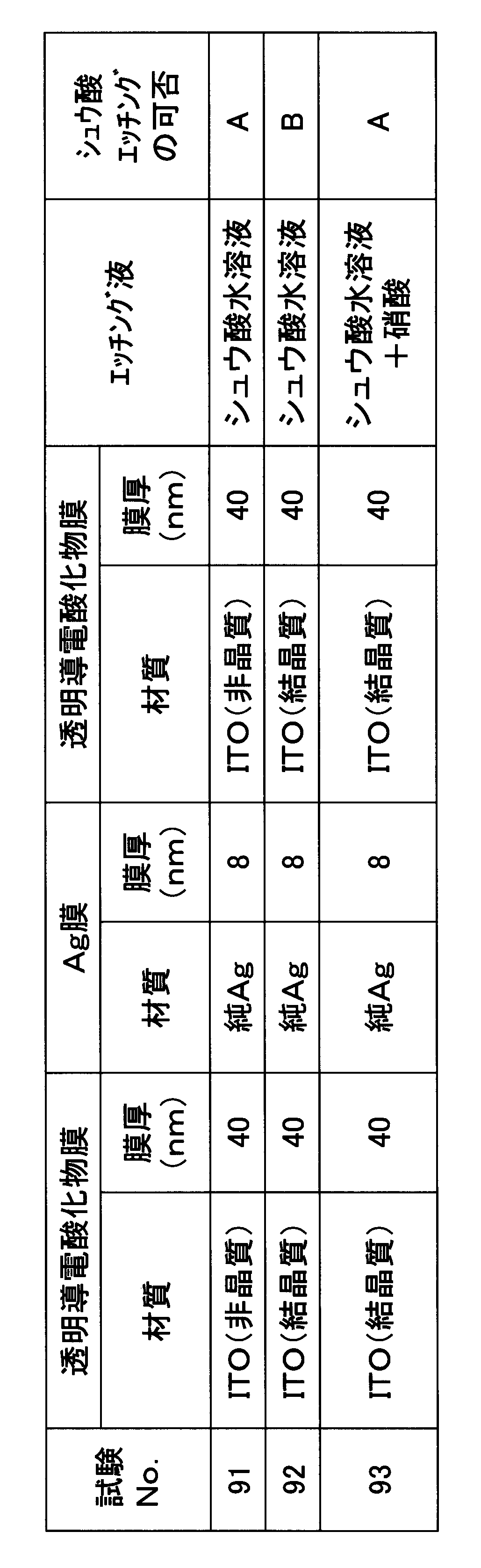
エッチング液としてシュウ酸水溶液を用いた場合には、透明導電酸化物膜として結晶質のITO膜を形成したNo.92においては、非晶質のITO膜を形成したNo.91に比べて、シュウ酸水溶液によるエッチング性に劣ることが確認される。なお、エッチング液としてシュウ酸水溶液と硝酸の混合液を用いた場合には、透明導電酸化物膜として結晶質のITO膜を形成したNo.93においても、エッチング性が良好であった。
以上の実験結果から、エッチング液としてシュウ酸水溶液を用いる場合には、透明導電酸化物膜を非晶質膜とすることが好ましいことが確認された。
以上の実験結果から、エッチング液としてシュウ酸水溶液を用いる場合には、透明導電酸化物膜を非晶質膜とすることが好ましいことが確認された。
(実施例4)
次に、実施例1のNo.1-7と同様の方法により、表4に示す構造の透明導電配線を製造した。なお、この実施例4では、ガラス基板上に透明導電酸化物膜を成膜し、その上にAg膜を成膜した2層構造とした。
No.101-117では、シュウ酸エッチング液によるエッチング処理後、残渣が確認されず、オーバーエッチング量は全て1μm以下であった。
得られた透明導電配線について、シート抵抗値を測定した。シート抵抗値の測定は、表面抵抗測定器(三菱油化社製、Loresta AP MCP-T400)を用いて四探針法により測定した。評価結果を表4に示す。
次に、実施例1のNo.1-7と同様の方法により、表4に示す構造の透明導電配線を製造した。なお、この実施例4では、ガラス基板上に透明導電酸化物膜を成膜し、その上にAg膜を成膜した2層構造とした。
No.101-117では、シュウ酸エッチング液によるエッチング処理後、残渣が確認されず、オーバーエッチング量は全て1μm以下であった。
得られた透明導電配線について、シート抵抗値を測定した。シート抵抗値の測定は、表面抵抗測定器(三菱油化社製、Loresta AP MCP-T400)を用いて四探針法により測定した。評価結果を表4に示す。
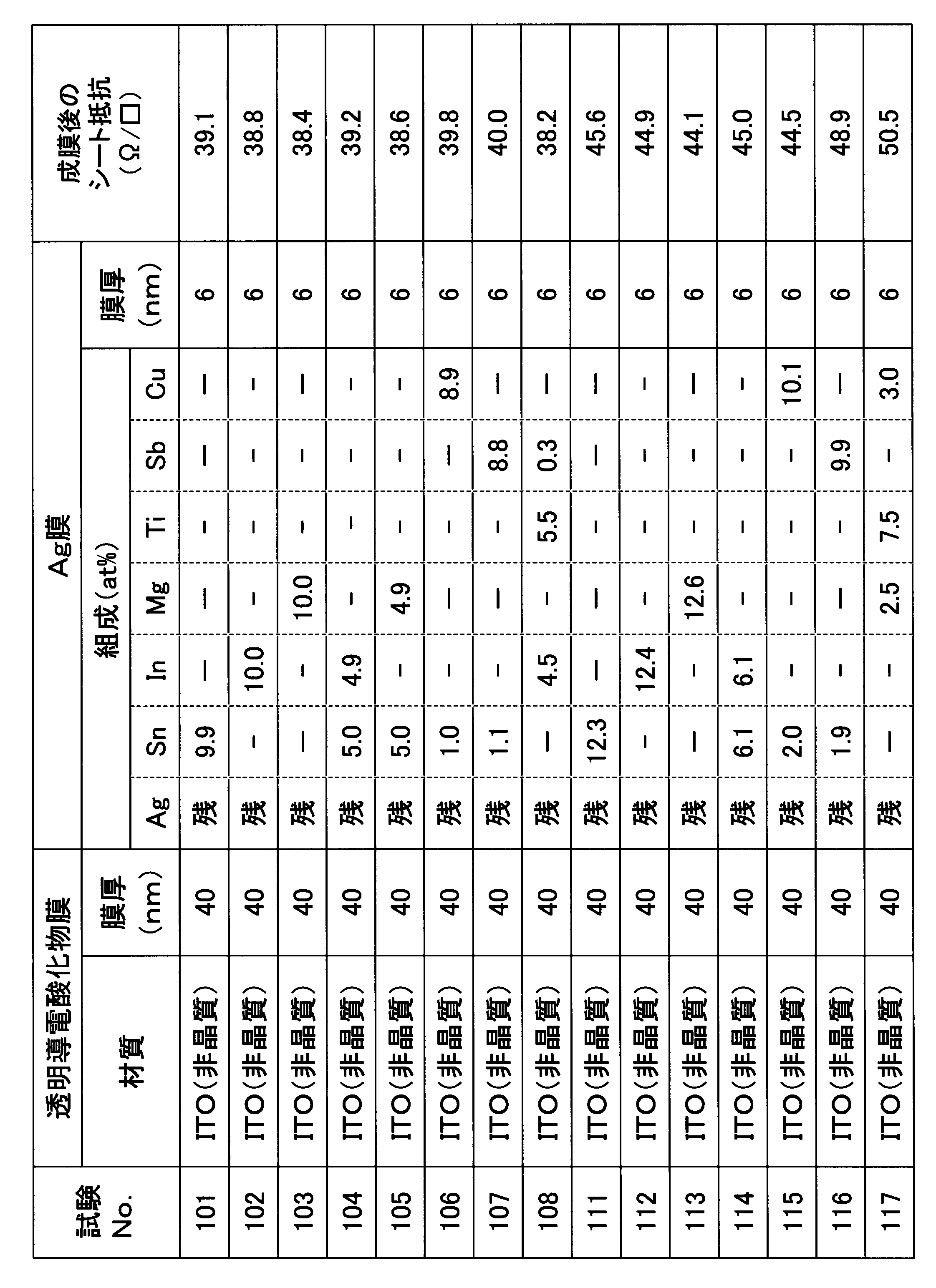
Ag膜を構成するAg合金の添加元素の合計量が10原子%を超えるNo.111-117においては、シート抵抗値が40Ω/sqを大きく上回っていた。一方、Ag膜を構成するAg合金の添加元素の合計量が10原子%以下とされたNo.101~108においては、シート抵抗値が40Ω/sq以下であった。
以上の実験結果から、特に、低抵抗の透明導電配線を得るためには、Ag膜を構成するAg合金の添加元素の合計量を10原子%以下に規定することが好ましいことが確認された。
以上の実験結果から、特に、低抵抗の透明導電配線を得るためには、Ag膜を構成するAg合金の添加元素の合計量を10原子%以下に規定することが好ましいことが確認された。
10、110 透明導電配線
11、111 Ag膜
12、112A、112B 透明導電酸化物膜
11、111 Ag膜
12、112A、112B 透明導電酸化物膜
Claims (6)
- Ag又はAg合金からなるAg膜とこのAg膜に積層された透明導電酸化物膜とを有し、エッチング処理によって配線パターンが形成された透明導電配線であって、
前記Ag膜の膜厚が15nm以下の範囲内とされ、
前記透明導電酸化物膜に対する前記Ag膜のオーバーエッチング量が1μm以下とされていることを特徴とする透明導電配線。 - 前記Ag膜は、添加元素としてSn、In、Mg、Tiのいずれか一種又は二種以上の元素を合計で0.05原子%以上、10.0原子%以下の範囲で含み、残部がAgおよび不可避不純物からなる組成のAg合金で構成されていることを特徴とする請求項1に記載の透明導電配線。
- 前記Ag膜は、添加元素としてさらにSb:0.01原子%以上、及び、Cu:0.1原子%以上のいずれか一方又は両方を含み、かつ、全添加元素の合計が10.0原子%以下とされ、残部がAgおよび不可避不純物からなる組成のAg合金で構成されていることを特徴とする請求項2に記載の透明導電配線。
- 前記透明導電酸化物膜は、非晶質膜とされていることを特徴とする請求項1から請求項3のいずれか一項に記載の透明導電配線。
- Ag又はAg合金からなるAg膜とこのAg膜に積層された透明導電酸化物膜とを有し、配線パターンが形成された透明導電配線の製造方法であって、
前記Ag膜の膜厚を15nm以下の範囲内とし、
前記Ag膜と前記透明導電酸化物膜とを有する積層膜に対してエッチング処理を行って配線パターンを形成するエッチング処理工程を有し、
このエッチング処理工程では、シュウ酸エッチング液を用いて、前記透明導電酸化物膜及び前記Ag膜を一括で溶解することを特徴とする透明導電配線の製造方法。 - 前記シュウ酸エッチング液は、シュウ酸濃度が3質量%以上7質量%以下の範囲内とされたシュウ酸水溶液とされていることを特徴とする請求項5に記載の透明導電配線の製造方法。
Priority Applications (2)
| Application Number | Priority Date | Filing Date | Title |
|---|---|---|---|
| CN201680002259.7A CN106796885B (zh) | 2015-02-27 | 2016-02-26 | 透明导电配线及透明导电配线的制造方法 |
| KR1020177004671A KR101777549B1 (ko) | 2015-02-27 | 2016-02-26 | 투명 도전 배선 및 투명 도전 배선의 제조 방법 |
Applications Claiming Priority (6)
| Application Number | Priority Date | Filing Date | Title |
|---|---|---|---|
| JP2015-037950 | 2015-02-27 | ||
| JP2015037950 | 2015-02-27 | ||
| JP2015-217683 | 2015-11-05 | ||
| JP2015217683 | 2015-11-05 | ||
| JP2016-034768 | 2016-02-25 | ||
| JP2016034768A JP6020750B1 (ja) | 2015-02-27 | 2016-02-25 | 透明導電配線、及び、透明導電配線の製造方法 |
Publications (1)
| Publication Number | Publication Date |
|---|---|
| WO2016136953A1 true WO2016136953A1 (ja) | 2016-09-01 |
Family
ID=56788764
Family Applications (1)
| Application Number | Title | Priority Date | Filing Date |
|---|---|---|---|
| PCT/JP2016/055855 Ceased WO2016136953A1 (ja) | 2015-02-27 | 2016-02-26 | 透明導電配線、及び、透明導電配線の製造方法 |
Country Status (1)
| Country | Link |
|---|---|
| WO (1) | WO2016136953A1 (ja) |
Cited By (2)
| Publication number | Priority date | Publication date | Assignee | Title |
|---|---|---|---|---|
| WO2018139402A1 (ja) * | 2017-01-25 | 2018-08-02 | Tdk株式会社 | アンテナ用透明導電フィルム |
| TWI904282B (zh) * | 2021-11-11 | 2025-11-11 | 日商Agc股份有限公司 | 附反射防止膜之透明基體及圖像顯示裝置 |
Citations (5)
| Publication number | Priority date | Publication date | Assignee | Title |
|---|---|---|---|---|
| JPH07114841A (ja) * | 1993-10-18 | 1995-05-02 | Toshiba Corp | 透明導電膜、その形成方法および透明導電膜の加工方法 |
| JPH09123337A (ja) * | 1995-03-22 | 1997-05-13 | Toppan Printing Co Ltd | 多層導電膜、並びにこれを用いた透明電極板および液晶表示装置 |
| JPH11302876A (ja) * | 1998-04-16 | 1999-11-02 | Nippon Sheet Glass Co Ltd | 透明導電膜の電極パターン加工方法 |
| JP2005250191A (ja) * | 2004-03-05 | 2005-09-15 | Idemitsu Kosan Co Ltd | 半透過・半反射電極基板、及びその製造方法、及びその半透過・半反射電極基板を用いた液晶表示装置 |
| JP2015030896A (ja) * | 2013-08-05 | 2015-02-16 | 出光興産株式会社 | スパッタリングターゲット及び酸化物透明導電膜 |
-
2016
- 2016-02-26 WO PCT/JP2016/055855 patent/WO2016136953A1/ja not_active Ceased
Patent Citations (5)
| Publication number | Priority date | Publication date | Assignee | Title |
|---|---|---|---|---|
| JPH07114841A (ja) * | 1993-10-18 | 1995-05-02 | Toshiba Corp | 透明導電膜、その形成方法および透明導電膜の加工方法 |
| JPH09123337A (ja) * | 1995-03-22 | 1997-05-13 | Toppan Printing Co Ltd | 多層導電膜、並びにこれを用いた透明電極板および液晶表示装置 |
| JPH11302876A (ja) * | 1998-04-16 | 1999-11-02 | Nippon Sheet Glass Co Ltd | 透明導電膜の電極パターン加工方法 |
| JP2005250191A (ja) * | 2004-03-05 | 2005-09-15 | Idemitsu Kosan Co Ltd | 半透過・半反射電極基板、及びその製造方法、及びその半透過・半反射電極基板を用いた液晶表示装置 |
| JP2015030896A (ja) * | 2013-08-05 | 2015-02-16 | 出光興産株式会社 | スパッタリングターゲット及び酸化物透明導電膜 |
Cited By (3)
| Publication number | Priority date | Publication date | Assignee | Title |
|---|---|---|---|---|
| WO2018139402A1 (ja) * | 2017-01-25 | 2018-08-02 | Tdk株式会社 | アンテナ用透明導電フィルム |
| JPWO2018139402A1 (ja) * | 2017-01-25 | 2019-11-21 | Tdk株式会社 | アンテナ用透明導電フィルム |
| TWI904282B (zh) * | 2021-11-11 | 2025-11-11 | 日商Agc股份有限公司 | 附反射防止膜之透明基體及圖像顯示裝置 |
Similar Documents
| Publication | Publication Date | Title |
|---|---|---|
| JP2016040411A (ja) | 積層膜、積層配線膜及び積層配線膜の製造方法 | |
| JP6888318B2 (ja) | 積層透明導電膜、積層配線膜及び積層配線膜の製造方法 | |
| KR101951045B1 (ko) | 액정표시장치용 어레이 기판의 제조방법 | |
| JP6020750B1 (ja) | 透明導電配線、及び、透明導電配線の製造方法 | |
| KR101805187B1 (ko) | 식각액 조성물 | |
| JP6135275B2 (ja) | 保護膜形成用スパッタリングターゲット | |
| KR102189087B1 (ko) | 보호막 형성용 스퍼터링 타깃 및 적층 배선막 | |
| JP6870332B2 (ja) | 積層透明導電膜、積層配線膜及び積層配線膜の製造方法 | |
| JP2016156087A (ja) | Cu積層膜、およびCu合金スパッタリングターゲット | |
| JP5724998B2 (ja) | 保護膜形成用スパッタリングターゲットおよび積層配線膜 | |
| CN105473760B (zh) | 保护膜形成用溅射靶及层叠配线膜 | |
| JP4655281B2 (ja) | 薄膜配線層 | |
| WO2016111202A1 (ja) | 積層膜 | |
| JP6565666B2 (ja) | 積層透明導電膜、積層配線膜及び積層配線膜の製造方法 | |
| JP6597284B2 (ja) | 積層透明導電膜、積層配線膜及び積層配線膜の製造方法 | |
| JP2016130010A (ja) | 積層膜 | |
| WO2017131183A1 (ja) | 積層透明導電膜、積層配線膜及び積層配線膜の製造方法 | |
| JP2018115349A (ja) | 保護膜形成用スパッタリングターゲット | |
| KR102245555B1 (ko) | 식각액 조성물 및 이를 이용한 투명 전극의 형성방법 | |
| WO2017164209A1 (ja) | 積層透明導電膜、積層配線膜及び積層配線膜の製造方法 | |
| JPWO2019093348A1 (ja) | 配線構造及びターゲット材 |
Legal Events
| Date | Code | Title | Description |
|---|---|---|---|
| 121 | Ep: the epo has been informed by wipo that ep was designated in this application |
Ref document number: 16755697 Country of ref document: EP Kind code of ref document: A1 |
|
| ENP | Entry into the national phase |
Ref document number: 20177004671 Country of ref document: KR Kind code of ref document: A |
|
| NENP | Non-entry into the national phase |
Ref country code: DE |
|
| 122 | Ep: pct application non-entry in european phase |
Ref document number: 16755697 Country of ref document: EP Kind code of ref document: A1 |