WO2016117613A1 - 接続体の製造方法、電子部品の接続方法、接続体 - Google Patents
接続体の製造方法、電子部品の接続方法、接続体 Download PDFInfo
- Publication number
- WO2016117613A1 WO2016117613A1 PCT/JP2016/051595 JP2016051595W WO2016117613A1 WO 2016117613 A1 WO2016117613 A1 WO 2016117613A1 JP 2016051595 W JP2016051595 W JP 2016051595W WO 2016117613 A1 WO2016117613 A1 WO 2016117613A1
- Authority
- WO
- WIPO (PCT)
- Prior art keywords
- light irradiation
- adhesive
- transparent substrate
- electronic component
- temporary
- Prior art date
- Legal status (The legal status is an assumption and is not a legal conclusion. Google has not performed a legal analysis and makes no representation as to the accuracy of the status listed.)
- Ceased
Links
Images





Classifications
-
- C—CHEMISTRY; METALLURGY
- C09—DYES; PAINTS; POLISHES; NATURAL RESINS; ADHESIVES; COMPOSITIONS NOT OTHERWISE PROVIDED FOR; APPLICATIONS OF MATERIALS NOT OTHERWISE PROVIDED FOR
- C09J—ADHESIVES; NON-MECHANICAL ASPECTS OF ADHESIVE PROCESSES IN GENERAL; ADHESIVE PROCESSES NOT PROVIDED FOR ELSEWHERE; USE OF MATERIALS AS ADHESIVES
- C09J11/00—Features of adhesives not provided for in group C09J9/00, e.g. additives
- C09J11/02—Non-macromolecular additives
- C09J11/06—Non-macromolecular additives organic
-
- C—CHEMISTRY; METALLURGY
- C09—DYES; PAINTS; POLISHES; NATURAL RESINS; ADHESIVES; COMPOSITIONS NOT OTHERWISE PROVIDED FOR; APPLICATIONS OF MATERIALS NOT OTHERWISE PROVIDED FOR
- C09J—ADHESIVES; NON-MECHANICAL ASPECTS OF ADHESIVE PROCESSES IN GENERAL; ADHESIVE PROCESSES NOT PROVIDED FOR ELSEWHERE; USE OF MATERIALS AS ADHESIVES
- C09J201/00—Adhesives based on unspecified macromolecular compounds
- C09J201/02—Adhesives based on unspecified macromolecular compounds characterised by the presence of specified groups, e.g. terminal or pendant functional groups
-
- C—CHEMISTRY; METALLURGY
- C09—DYES; PAINTS; POLISHES; NATURAL RESINS; ADHESIVES; COMPOSITIONS NOT OTHERWISE PROVIDED FOR; APPLICATIONS OF MATERIALS NOT OTHERWISE PROVIDED FOR
- C09J—ADHESIVES; NON-MECHANICAL ASPECTS OF ADHESIVE PROCESSES IN GENERAL; ADHESIVE PROCESSES NOT PROVIDED FOR ELSEWHERE; USE OF MATERIALS AS ADHESIVES
- C09J5/00—Adhesive processes in general; Adhesive processes not provided for elsewhere, e.g. relating to primers
-
- C—CHEMISTRY; METALLURGY
- C09—DYES; PAINTS; POLISHES; NATURAL RESINS; ADHESIVES; COMPOSITIONS NOT OTHERWISE PROVIDED FOR; APPLICATIONS OF MATERIALS NOT OTHERWISE PROVIDED FOR
- C09J—ADHESIVES; NON-MECHANICAL ASPECTS OF ADHESIVE PROCESSES IN GENERAL; ADHESIVE PROCESSES NOT PROVIDED FOR ELSEWHERE; USE OF MATERIALS AS ADHESIVES
- C09J5/00—Adhesive processes in general; Adhesive processes not provided for elsewhere, e.g. relating to primers
- C09J5/06—Adhesive processes in general; Adhesive processes not provided for elsewhere, e.g. relating to primers involving heating of the applied adhesive
-
- C—CHEMISTRY; METALLURGY
- C09—DYES; PAINTS; POLISHES; NATURAL RESINS; ADHESIVES; COMPOSITIONS NOT OTHERWISE PROVIDED FOR; APPLICATIONS OF MATERIALS NOT OTHERWISE PROVIDED FOR
- C09J—ADHESIVES; NON-MECHANICAL ASPECTS OF ADHESIVE PROCESSES IN GENERAL; ADHESIVE PROCESSES NOT PROVIDED FOR ELSEWHERE; USE OF MATERIALS AS ADHESIVES
- C09J9/00—Adhesives characterised by their physical nature or the effects produced, e.g. glue sticks
- C09J9/02—Electrically-conducting adhesives
-
- H—ELECTRICITY
- H05—ELECTRIC TECHNIQUES NOT OTHERWISE PROVIDED FOR
- H05K—PRINTED CIRCUITS; CASINGS OR CONSTRUCTIONAL DETAILS OF ELECTRIC APPARATUS; MANUFACTURE OF ASSEMBLAGES OF ELECTRICAL COMPONENTS
- H05K3/00—Apparatus or processes for manufacturing printed circuits
- H05K3/30—Assembling printed circuits with electric components, e.g. with resistors
- H05K3/32—Assembling printed circuits with electric components, e.g. with resistors electrically connecting electric components or wires to printed circuits
-
- H—ELECTRICITY
- H10—SEMICONDUCTOR DEVICES; ELECTRIC SOLID-STATE DEVICES NOT OTHERWISE PROVIDED FOR
- H10W—GENERIC PACKAGES, INTERCONNECTIONS, CONNECTORS OR OTHER CONSTRUCTIONAL DETAILS OF DEVICES COVERED BY CLASS H10
- H10W74/00—Encapsulations, e.g. protective coatings
- H10W74/10—Encapsulations, e.g. protective coatings characterised by their shape or disposition
- H10W74/15—Encapsulations, e.g. protective coatings characterised by their shape or disposition on active surfaces of flip-chip devices, e.g. underfills
Definitions
- the present invention relates to a method for producing a connection body in which an electronic component is connected on a transparent substrate via a circuit connection adhesive containing a photopolymerization initiator, and via a circuit connection adhesive containing a photopolymerization initiator.
- the present invention relates to a connection method for connecting an electronic component on a transparent substrate and a connection body manufactured using the connection method.
- liquid crystal display devices are often used as various display means such as televisions, PC monitors, mobile phones, portable game machines, tablet PCs, and in-vehicle monitors.
- COG chip on glass
- a liquid crystal driving IC is directly mounted on a substrate of a liquid crystal display panel or a liquid crystal driving circuit from the viewpoints of fine pitch, light weight, and thinning.
- FOG film on ⁇ ⁇ glass
- the flexible substrate on which is formed is directly mounted on the substrate of the liquid crystal display panel.
- a liquid crystal display device 100 employing a COG mounting system has a liquid crystal display panel 104 that performs a main function for liquid crystal display.
- the liquid crystal display panel 104 is a glass substrate or the like. And two transparent substrates 102 and 103 facing each other.
- the transparent substrates 102 and 103 are bonded to each other by a frame-shaped seal 105, and the liquid crystal 106 is sealed in a space surrounded by the transparent substrates 102 and 103 and the seal 105.
- a panel display unit 107 is provided.
- the transparent substrates 102 and 103 have a pair of striped transparent electrodes 108 and 109 made of ITO (Indium Tin Oxide) or the like on both inner surfaces facing each other so as to intersect each other.
- the transparent substrates 102 and 103 are configured such that a pixel as a minimum unit of liquid crystal display is constituted by the intersection of the transparent electrodes 108 and 109.
- one transparent substrate 103 is formed to have a larger planar dimension than the other transparent substrate 102, and the transparent electrode 109 is formed on the edge 103a of the transparent substrate 103 formed to be large. Terminal portion 109a is formed.
- alignment films 111 and 112 subjected to a predetermined rubbing process are formed on both transparent electrodes 108 and 109, and the initial alignment of liquid crystal molecules is regulated by the alignment films 111 and 112. ing.
- a pair of polarizing plates 118 and 119 are disposed outside the transparent electrodes 108 and 109, and the vibration direction of transmitted light from the light source 120 such as a backlight is regulated by the polarizing plates 118 and 119. It has come to be.
- the liquid crystal driving IC 115 is thermocompression-bonded on the terminal portion 109a via an anisotropic conductive film 114.
- the anisotropic conductive film 114 is a film formed by mixing conductive particles in a thermosetting binder resin, and heat conduction is performed between the two conductors so that the electrical conduction between the conductors is achieved by the conductive particles. And the mechanical connection between the conductors is maintained by the binder resin.
- the liquid crystal driving IC 115 can perform predetermined liquid crystal display by selectively changing the alignment of the liquid crystal by selectively applying a liquid crystal driving voltage to the pixels.
- the adhesive constituting the anisotropic conductive film 114 the most reliable thermosetting adhesive is usually used.
- the anisotropic conductive film 114 is attached to the terminal portion 109a of the transparent electrode 109 by a temporary crimping means (not shown). Temporarily crimp. Subsequently, after the liquid crystal driving IC 115 is placed on the anisotropic conductive film 114, the liquid crystal driving IC 115 is connected to the terminal together with the anisotropic conductive film 114 by thermocompression bonding means 121 such as a thermocompression bonding head as shown in FIG. The thermocompression bonding means 121 is caused to generate heat while being pressed toward the portion 109a.
- the anisotropic conductive film 114 undergoes a thermosetting reaction, whereby the liquid crystal driving IC 115 is bonded onto the terminal portion 109a via the anisotropic conductive film 114.
- the heat pressing temperature is high, and the thermal shock to the electronic components such as the liquid crystal driving IC 115 and the transparent substrate 103 is increased.
- the anisotropic conductive film is connected, when the temperature decreases to room temperature, the binder contracts due to the temperature difference, and the terminal portion 109a of the transparent substrate 103 may be warped. For this reason, there is a risk of causing problems such as uneven display and poor connection of the liquid crystal driving IC 115.
- Patent Document 2 in a method of bonding a connection target object and a connection target object via a photo-curing adhesive, light irradiation is performed after the start of heat pressing by a heating press head.
- connection method using an ultraviolet curable adhesive instead of the anisotropic conductive film 114 using such a thermosetting adhesive has been proposed.
- the adhesive softens and flows due to heat, and the temperature is sufficient to capture the conductive particles between the terminal portion 109a of the transparent electrode 109 and the electrode of the liquid crystal driving IC 115. Only heat, cure the adhesive by UV irradiation.
- misalignment occurs when an electronic component such as the liquid crystal driving IC 115 is mounted and pressed by the thermocompression bonding means 112 or when the thermocompression bonding means 112 is separated from the liquid crystal driving IC 115.
- an electronic component such as the liquid crystal driving IC 115 is mounted and pressed by the thermocompression bonding means 112 or when the thermocompression bonding means 112 is separated from the liquid crystal driving IC 115.
- the misalignment is caused by the electrode terminals of the liquid crystal driving IC 115 and the terminal portions of the transparent substrate 103 connected to the electrode terminals.
- the pitch with the terminal portion adjacent to 109a is narrowed, which may cause a short circuit between the terminals that is short-circuited through the conductive particles.
- an anisotropic conductive film 1 When an anisotropic conductive film 1 is used to connect an electronic component having a relatively low rigidity such as the flexible substrate 21 to the transparent substrate 12, it is bonded by the heat of the pressing head as in the technique described in Patent Document 2.
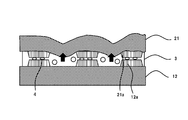
- pressure is applied in a state where the viscosity of the agent is sufficiently lowered, the stress remains due to bending between the terminals 21a of the flexible substrate 21 indicated by arrows in FIG.
- the flexible substrate 21 releases the residual stress of the flexible substrate 21 when the heating and pressing head 30 is separated (pressed out), and the terminal 21a is pressed between the terminals 21a by the residual stress of the flexible substrate 21 as shown in FIG.
- the force to return in the opposite direction works. Then, when the residual stress of the flexible substrate 21 is released, as shown in FIG.
- peeling between the terminals 21 a of the flexible substrate 21 at the interface between the binder resin layer 3 of the anisotropic conductive film and the flexible substrate 21 is likely to occur. Such peeling may lead to a connection failure such as a decrease in the conduction resistance value of the connection body and a decrease in the adhesive force between the anisotropic conductive film and the adherend.
- a soft binder resin that spreads sufficiently during crimping that is, a binder resin having a low viscosity, in order to ensure adhesive strength.
- a binder resin having a low viscosity in order to ensure adhesive strength.
- the viscosity of the binder resin is lowered too much, the flexible substrate between the wirings is more easily bent at the time of crimping, and the influence of releasing the residual stress of the flexible substrate tends to appear more conspicuously.
- the present invention solves the above-described problems, and uses a photo-curing adhesive to connect electronic components at a low temperature, prevent misalignment of the electronic components, and improve connection failure. It is an object of the present invention to provide a manufacturing method, a connection method of electronic parts, and a connection body manufactured using the same.
- a method for manufacturing a connection body includes an adhesive placement step of providing a circuit connection adhesive containing a photopolymerization initiator on a transparent substrate, and the circuit connection adhesive.
- An electronic component is disposed on the transparent substrate through a light irradiation step of irradiating the adhesive for circuit connection with light, and heating and light irradiation are performed while pressing the electronic component against the transparent substrate.
- the light irradiation amount in the light irradiation step is smaller than the light irradiation amount in the main pressure bonding step.
- the method for manufacturing a connection body includes an adhesive placement step of providing a circuit connection adhesive containing a photopolymerization initiator on a transparent substrate, and the circuit connection adhesive on the transparent substrate. Placing the electronic component on the substrate, pressing the electronic component onto the transparent substrate, and applying a light to the circuit connecting adhesive, and a temporary pressure bonding step, while pressing the electronic component against the transparent substrate, A main pressure-bonding step for performing heating and light irradiation, and the light irradiation amount in the temporary pressure-bonding step is smaller than the light irradiation amount in the main pressure-bonding step.
- the electronic component connection method includes an adhesive placement step of providing a circuit connection adhesive containing a photopolymerization initiator on a transparent substrate, and the circuit connection adhesive on the transparent substrate.
- the light irradiation amount in the light irradiation step is smaller than the light irradiation amount in the main compression bonding step.
- connection body according to the present invention is manufactured by the above-described electronic component connection method.
- curing is started by irradiating light with an appropriate irradiation amount to an adhesive for circuit connection containing a photopolymerization initiator, and the electronic component is temporarily crimped in a state where the viscosity is increased. Can do. Therefore, in the light irradiation process (temporary crimping process) and the main crimping process, when the electronic component is pressed by the crimping tool or when the crimping tool is separated from the electronic component, the electronic component is displaced from a predetermined position. Can be suppressed.
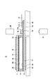
- FIG. 1 is a cross-sectional view showing a mounting process to which the present invention is applied.
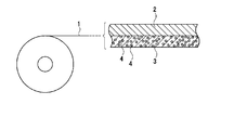
- FIG. 2 is a cross-sectional view showing an anisotropic conductive film.
- FIG. 3 is a cross-sectional view showing a temporary sticking step of the anisotropic conductive film.
- FIG. 4 is a cross-sectional view showing a process of disposing the liquid crystal driving IC on the transparent substrate.
- FIG. 5 is a cross-sectional view showing a temporary press-bonding process of the liquid crystal driving IC.
- FIG. 6 is a cross-sectional view showing the final press-bonding step of the liquid crystal driving IC.
- FIG. 7 is a cross-sectional view showing a connection body in which a liquid crystal driving IC is connected on a transparent substrate.
- FIG. 8 is a cross-sectional view showing an example of a process of disposing a flexible substrate on a transparent substrate via an anisotropic conductive film.
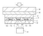
- FIG. 9 is a cross-sectional view showing an example of a process of irradiating the anisotropic conductive film with ultraviolet light after disposing a flexible substrate on the transparent substrate via the anisotropic conductive film.
- FIG. 10 is a cross-sectional view showing an example of the main crimping process of the flexible substrate.
- FIG. 11 is a diagram for explaining a method of measuring conduction resistance according to the example and the comparative example.
- FIG. 12 is a diagram for explaining a method of measuring the amount of misalignment in the width direction of the terminals of the connection body sample.
- FIG. 13 is a diagram for explaining the timing of light irradiation before the main pressure bonding, light irradiation at the time of the main pressure bonding, and thermal pressurization in the second embodiment.
- FIG. 14 is a cross-sectional view showing a conventional liquid crystal display panel.
- FIG. 15 is a cross-sectional view showing a COG mounting process of a conventional liquid crystal display panel.
- FIG. 16 is sectional drawing which shows an example of the heating press process of a laminated body in the manufacturing method of the conventional flexible substrate.
- FIG. 17 is a cross-sectional view showing an example of a laminated body in a state in which stress is released at the time of press-out of a heating tool in a conventional flexible substrate manufacturing method.
- FIG. 18 is a cross-sectional view showing an example of a laminated body in a state in which residual stress is released in the flexible substrate in the conventional method for manufacturing a flexible substrate.
- connection body a method for manufacturing a connection body, a method for connecting an electronic component, and a connection body to which the present invention is applied will be described in detail with reference to the drawings.
- the present invention is not limited to the following embodiments, and various modifications can be made without departing from the scope of the present invention.
- the drawings are schematic, and the ratio of each dimension may be different from the actual one. Specific dimensions should be determined in consideration of the following description. Moreover, it is a matter of course that portions having different dimensional relationships and ratios are included between the drawings.
- the liquid crystal display panel 10 includes two transparent substrates 11 and 12 made of a glass substrate and the like, and the transparent substrates 11 and 12 are bonded to each other by a frame-shaped seal 13. .
- the liquid crystal 14 is sealed in a space surrounded by the transparent substrates 11 and 12 to form a panel display unit 15.
- the transparent substrates 11 and 12 have a pair of striped transparent electrodes 16 and 17 made of ITO (Indium Tin Oxide) or the like on both inner surfaces facing each other so as to intersect each other.
- the transparent electrodes 16 and 17 are configured such that a pixel as a minimum unit of liquid crystal display is configured by the intersection of the transparent electrodes 16 and 17.
- one transparent substrate 12 is formed to have a larger planar dimension than the other transparent substrate 11, and an edge 12a of the formed transparent substrate 12 has an electronic component.
- a COG mounting portion 20 on which the liquid crystal driving IC 18 is mounted is provided, and an FOG mounting portion 22 on which a flexible substrate 21 on which a liquid crystal driving circuit is formed as an electronic component is mounted is provided near the outside of the COG mounting portion 20. It has been.
- liquid crystal driving IC and the liquid crystal driving circuit can perform predetermined liquid crystal display by selectively changing the alignment of the liquid crystal by selectively applying the liquid crystal driving voltage to the pixels. ing.
- the terminal portions 17a of the transparent electrodes 17 are formed on the mounting portions 20 and 22, respectively.
- the liquid crystal driving IC 18 and the flexible substrate 21 are connected using the anisotropic conductive film 1 as an adhesive for circuit connection containing a photopolymerization initiator.
- the anisotropic conductive film 1 contains the conductive particles 4, and includes the liquid crystal driving IC 18 and the electrode of the flexible substrate 21 and the terminal portion 17 a of the transparent electrode 17 formed on the edge portion 12 a of the transparent substrate 12. Electrical connection is made through the conductive particles 4.
- the anisotropic conductive film 1 is an ultraviolet curable adhesive, and is fluidized by being thermocompression bonded by a heating and pressing head 30 described later, whereby the conductive particles 4 are converted into terminal portions 17a, a liquid crystal driving IC 18 and a flexible substrate. By being crushed between the respective electrodes 21 and being irradiated with ultraviolet rays by the ultraviolet irradiator 31, the conductive particles 4 are cured in a crushed state. Thereby, the anisotropic conductive film 1 electrically and mechanically connects the transparent substrate 12 to the liquid crystal driving IC 18 and the flexible substrate 21.
- an alignment film 24 subjected to a predetermined rubbing process is formed on both the transparent electrodes 16 and 17, and the initial alignment of liquid crystal molecules is regulated by the alignment film 24.
- a pair of polarizing plates 25 and 26 are disposed outside the transparent substrates 11 and 12, and these polarizing plates 25 and 26 allow transmitted light from a light source (not shown) such as a backlight to be transmitted. The vibration direction is regulated.
- an anisotropic conductive film (ACF) 1 is usually formed with a binder resin layer (adhesive layer) 3 containing conductive particles on a release film 2 as a base material. It has been done.
- the anisotropic conductive film 1 has a binder resin layer 3 interposed between a transparent electrode 17 formed on a transparent substrate 12 of the liquid crystal display panel 10 and a liquid crystal driving IC 18 or a flexible substrate 21. As a result, the liquid crystal display panel 10 and the liquid crystal driving IC 18 or the flexible substrate 21 are connected and made conductive.
- a substrate such as a polyethylene terephthalate film generally used in anisotropic conductive films can be used.
- the binder resin layer 3 is formed by dispersing conductive particles 4 in a binder.
- the binder contains a film-forming resin, a curable resin, a curing agent, a silane coupling agent, and the like, and is the same as the binder used for a normal anisotropic conductive film.
- the film forming resin is preferably a resin having an average molecular weight of about 10,000 to 80,000.
- the film forming resin include various resins such as a phenoxy resin, an epoxy resin, a modified epoxy resin, and a urethane resin.
- phenoxy resin is particularly preferable from the viewpoint of film formation state, connection reliability, and the like.
- the curable resin is not particularly limited, and examples thereof include an epoxy resin and an acrylic resin.
- an epoxy resin there is no restriction
- naphthalene type epoxy resin, biphenyl type epoxy resin, phenol novolac type epoxy resin, bisphenol type epoxy resin, stilbene type epoxy resin, triphenolmethane type epoxy resin, phenol aralkyl type epoxy resin, naphthol type epoxy resin, A dicyclopentadiene type epoxy resin, a triphenylmethane type epoxy resin, etc. are mentioned. These may be used alone or in combination of two or more.
- an acrylic resin there is no restriction
- the curing agent is not particularly limited as long as it is a photo-curing type, and can be appropriately selected according to the purpose.
- the curable resin is an epoxy resin
- a cationic curing agent is preferable, and an anionic curing agent is used. May be.
- the curable resin is an acrylic resin
- a radical curing agent is preferable.
- the curable resin may include an epoxy resin and an acrylic resin.
- curing agent there is no restriction
- curing agent For example, a sulfonium salt, onium salt, etc. can be mentioned, Among these, an aromatic sulfonium salt is preferable.
- curing agent According to the objective, it can select suitably, For example, an organic peroxide can be mentioned.
- silane coupling agents include epoxy, amino, mercapto sulfide, ureido and the like. By adding the silane coupling agent, the adhesion at the interface between the organic material and the inorganic material is improved.
- Examples of the conductive particles 4 include any known conductive particles used in anisotropic conductive films.
- Examples of the conductive particles 4 include particles of various metals and metal alloys such as nickel, iron, copper, aluminum, tin, lead, chromium, cobalt, silver, gold, metal oxide, carbon, graphite, glass, ceramic, Examples thereof include those in which the surface of particles such as plastic is coated with metal, or those in which the surface of these particles is further coated with an insulating thin film.
- examples of the resin particle include an epoxy resin, a phenol resin, an acrylic resin, an acrylonitrile / styrene (AS) resin, a benzoguanamine resin, a divinylbenzene resin, a styrene resin, and the like. Can be mentioned.
- the anisotropic conductive film 1 is temporarily pasted on the transparent substrate 12 (adhesive placement step). As shown in FIG. 3, the anisotropic conductive film 1 is temporarily attached to the transparent electrode 17 of the transparent substrate 12 so that the binder resin layer 3 is on the transparent electrode 17 side. Deploy. After arranging the binder resin layer 3 on the transparent electrode 17, the binder resin layer 3 is heated and pressed from the release film 2 side with, for example, a thermocompression tool, the thermocompression tool is separated from the release film 2, and the release film 2 is bonded to the binder resin. Peel from layer 3. In addition, temporary sticking of the anisotropic conductive film 1 may be performed by the pressurization and light irradiation by a thermocompression bonding tool, and may be performed using heat pressurization and light irradiation together.
- the liquid crystal driving IC 18 is disposed on the transparent substrate 12 through the anisotropic conductive film 1, and the liquid crystal driving IC 18 is pressed against the transparent substrate 12 and light is applied to the anisotropic conductive film 1 ( Temporary crimping process).
- the liquid crystal driving IC 18 and the transparent electrode 17 are aligned. Specifically, the liquid crystal driving IC is arranged so that each terminal portion 17a of the transparent electrode 17 and the electrode terminal 18a of the liquid crystal driving IC 18 face each other with the binder resin layer 3 interposed therebetween.
- the upper surface of the liquid crystal driving IC 18 is cooled by a thermocompression bonding tool 30 that has been heated to a predetermined heating temperature via a buffer material 32 at a lower temperature and lower pressure than the main pressure bonding process described later. While heat-pressing, the binder resin layer 3 of the anisotropic conductive film 1 is irradiated with ultraviolet rays by an ultraviolet irradiator 31 provided on the back side of the transparent substrate 12.
- the heat pressing temperature by the thermocompression bonding tool 30 is a temperature of ⁇ 10 to 20 ° C. (for example, around 80 ° C.) with respect to a predetermined temperature indicating the viscosity (minimum melt viscosity) when the binder resin layer is melted before the start of curing. Set to Thereby, the warp of the transparent substrate is minimized, and the liquid crystal driving IC is not damaged by heat.
- the ultraviolet light emitted from the ultraviolet irradiator 31 passes through a transparent support base such as glass supporting the transparent substrate 12 and the transparent substrate 12 supported by the support base and is irradiated to the binder resin layer 3.
- a transparent support base such as glass supporting the transparent substrate 12 and the transparent substrate 12 supported by the support base and is irradiated to the binder resin layer 3.
- an LED lamp, a mercury lamp, a metal halide lamp, or the like can be used as the ultraviolet irradiator 31.
- the ultraviolet irradiation amount in the temporary bonding step is preferably 3 to 15 mW / cm 2 and 0.5 to 2 seconds.
- the temporary press-bonding step it is preferable to change the light irradiation amount by the minimum inter-wiring space (minimum bump space) of the liquid crystal driving IC 18.
- the minimum inter-wiring space of the liquid crystal driving IC 18 is 8 to 20 ⁇ m
- the light irradiation amount in the temporary pressing step is 4 to 20% of the light irradiation amount in the main pressing step.
- the pressing force to the liquid crystal driving IC 18 in the temporary pressing step is preferably 40 to 90%, more preferably 70 to 80% of the pressing force to the liquid crystal driving IC 18 in the main pressing step.
- the anisotropic conductive film 1 is irradiated with ultraviolet rays at an appropriate dose to start the curing of the binder resin layer 3, and the liquid crystal driving IC 18 is temporarily pressed in a state where the viscosity is increased. be able to. Therefore, when the liquid crystal driving IC 18 is pressed by the thermocompression bonding tool 30 or when the thermocompression bonding tool 30 is separated from the liquid crystal driving IC 18 in the temporary pressure bonding process or the main pressure bonding process described later, the liquid crystal driving IC 18 is predetermined. It is possible to suppress misalignment from the position.
- the binder resin flows out from between the electrode terminal 18a of the liquid crystal driving IC 18 and the terminal portion 17a of the transparent electrode 17, and conduction is achieved by sandwiching the conductive particles 4 in this state. Is cured.
- the liquid crystal display panel 10 is formed as a connection body in which the liquid crystal driving IC 18 is electrically and mechanically connected to the transparent substrate 12.
- the viscosity of the binder resin can be increased to some extent by irradiating the anisotropic conductive film 1 with ultraviolet rays at a dose smaller than the light dose in the final crimping step in the temporary crimping step. Therefore, it is possible to prevent misalignment of the liquid crystal driving IC 18 when the thermocompression bonding tool 30 is pressed or when the thermocompression bonding tool 30 is separated. Therefore, the pitch between the electrode terminal 18a of the liquid crystal driving IC 18 having a fine pitch and the terminal part adjacent to the terminal part 17a of the transparent electrode 17 connected to the electrode terminal 18a is narrowed, and the conductive particles 4 are interposed. It is possible to prevent a short circuit between terminals that is short-circuited.
- the illuminance in the temporary bonding step may be lower than the illuminance in the temporary pressure bonding step.
- ultraviolet irradiation may be performed not from the transparent substrate 12 side but from the liquid crystal driving IC 18 side in the provisional pressure bonding step described above.
- This manufacturing method includes a step of providing the anisotropic conductive film 1 on the transparent substrate 12, a step of disposing the liquid crystal driving IC 18 on the anisotropic conductive film 1, and a step of performing light irradiation from the liquid crystal driving IC 18 side. (Light irradiation step) and a step of heating and light irradiation (main pressure bonding step) while pressing the liquid crystal driving IC 18 against the transparent substrate 12, and the light irradiation amount in the light irradiation step is the main pressure bonding. You may make it become smaller than the light irradiation amount in a process.
- This manufacturing method may further include a step of pressing the liquid crystal driving IC 18 with a heating tool before and after the light irradiation step in Specific Example 1-3.
- This manufacturing method differs between the step of providing the anisotropic conductive film 1 on the transparent substrate 12 and the step of disposing the liquid crystal driving IC 18 on the anisotropic conductive film 1 in Specific Example 1-3. You may further have the process of light-irradiating with respect to the anisotropic conductive film 1 whole surface.
- This manufacturing method includes a step of providing the anisotropic conductive film 1 on the transparent substrate 12 and a step of irradiating the entire surface of the anisotropic conductive film 1 from the side of the anisotropic conductive film 1 (pre-irradiation step). A step of disposing the liquid crystal driving IC 18 on the anisotropic conductive film 1 after the pre-irradiation step, a step of performing light irradiation from the transparent substrate 12 side (light irradiation step), and a liquid crystal driving IC 18 on the transparent substrate 12.
- the process includes a step of heating and light irradiation (main pressure bonding step) while pressing against the light, and the total amount of light irradiation in the first irradiation step and the light irradiation step is smaller than the light irradiation amount in the main pressure bonding step. You may do it.
- This manufacturing method as an example includes a step of providing an anisotropic conductive film on a transparent substrate, and a flexible substrate is disposed on the transparent substrate via the anisotropic conductive film, and the anisotropic conductive film is irradiated with light. And a step of performing heating and light irradiation while pressing the flexible substrate against the transparent substrate.
- the temporary sticking step can be performed in the same manner as the temporary sticking step in the first embodiment described above.
- the flexible substrate 21 is disposed on the transparent substrate 12 via the anisotropic conductive film 1, and the anisotropic conductive film 1 is irradiated with light.
- the light irradiation can be performed by irradiating the binder resin layer 3 of the anisotropic conductive film 1 with ultraviolet rays by an ultraviolet irradiator 31 disposed on the transparent substrate 12 side.
- the light irradiation may be performed not from the transparent substrate 12 side but from the flexible substrate 21 side.
- the amount of ultraviolet light irradiated to the anisotropic conductive film 1 is made smaller than the amount of light irradiated in the main press-bonding step described later.
- the light irradiation amount in the light irradiation step is preferably 5 to 25% of the light irradiation amount in the main pressure bonding step, and is 5 to 15%. More preferably.
- the light irradiation amount in the light irradiation step is preferably 2 to 15% of the light irradiation amount in the main pressure bonding step. More preferably, it is 10%.
- the ultraviolet illuminance and the ultraviolet irradiation time irradiated in the light irradiation step can be appropriately selected within a range that satisfies the above-described conditions.
- the ultraviolet illuminance can be 1 to 400 mW / cm 2 and the ultraviolet irradiation time can be 0.5 to 2 seconds.
- the light irradiation time in the light irradiation step is 1/5 or less of the pressure bonding time in the main pressure bonding step. It is preferable.
- the flexible substrate 21 is disposed so that each terminal portion 17 a of the transparent electrode 17 and the terminal portion 21 a of the flexible substrate 21 face each other with the binder resin layer 3 interposed therebetween.
- the upper surface of the flexible substrate 21 is heat-pressed through a buffer material 32 by a thermocompression bonding tool 30 that has been heated to a predetermined heating temperature, and is changed by an ultraviolet irradiator 31 provided on the back side of the transparent substrate 12.
- the binder resin layer 3 of the anisotropic conductive film 1 is irradiated with ultraviolet rays.
- the thermal pressurization in the main press-bonding step is performed with a predetermined pressure that causes the conductive particles 4 to be sandwiched between the terminal portion 21 a of the flexible substrate 21 and the terminal portion 17 a of the transparent electrode 17.
- the light irradiation in this press-fit process is performed on the conditions which can harden the binder resin layer 3.
- the binder of the anisotropic conductive film 1 is made before the main pressure bonding step by making the light irradiation amount in the light irradiation step smaller than the light irradiation amount in the main pressure bonding step. Since the viscosity of the resin is increased to some extent, it is possible to prevent misalignment of the flexible substrate 21 when pressing with the thermocompression bonding tool 30 or when the thermocompression bonding tool 30 is separated.
- connection failures such as a decrease in the conductive resistance value of the connection body and a decrease in the adhesive force between the anisotropic conductive film and the adherend can be suppressed.
- the viscosity of the binder resin of the anisotropic conductive film is not adjusted each time according to the wiring layout of the flexible substrate and the minimum inter-wiring space, the residual stress is released depending on the light irradiation conditions. The influence can be suppressed. Therefore, the manufacturing efficiency of the connection body can be further improved.
- the binder resin layer of the anisotropic conductive film 1 is applied by the ultraviolet irradiator 31 while being thermally pressed at a lower temperature and lower pressure than the main pressure bonding step with a thermocompression bonding tool.
- 3 may be irradiated with ultraviolet rays.
- the heat pressurization temperature and the pressing force by the thermocompression bonding tool can be set to the same conditions as those in the provisional pressure bonding step in the first embodiment described above, for example.
- This manufacturing method may further include a step of pressing the flexible substrate 21 with a heating tool before and after the light irradiation step in the specific example 2-1.
- This manufacturing method includes a step of temporarily attaching the anisotropic conductive film 1 on the transparent substrate 12, a step of performing light irradiation on the entire surface of the anisotropic conductive film 1 (pre-irradiation step), and a step after the pre-irradiation step.
- an anisotropic conductive film comprising a binder resin layer containing a photoacid generator and a cationic polymerizable compound was prepared.
- This binder resin layer Phenoxy resin (YP-50: manufactured by Nippon Steel & Sumikin Chemical Co., Ltd.); 45 parts by mass isocyanuric acid EO-modified diacrylate (M-215: manufactured by Toagosei Co., Ltd.); 45 parts by mass of silane coupling agent (KBM-403: Shin-Etsu Chemical) Manufactured by Kogyo Co., Ltd.); 2 parts by mass photoradical generator (Irgacure 369: manufactured by BASF Japan Co., Ltd.); Particles (AUL 704: average particle diameter of 4 ⁇ m, manufactured by Sekisui Chemical Co., Ltd.) were dispersed so that the particle density was about 50,000 particles / mm 2 .
- This mixed solution was applied onto a 50 ⁇ m thick PET film, dried in an oven at 70 ° C. for 5 minutes, and formed into a 20 ⁇ m thick film.
- IC As an evaluation element, External shape: 1.8 mm ⁇ 20 mm, Bump height: 15 ⁇ m, Bump size: 30 ⁇ 60 ⁇ m (minimum bump space 10 ⁇ m), IC for evaluation was used.
- the bumps are arranged inside the both ends of the evaluation IC outer shape in the long side direction so that the short side of the bump is parallel to the long side direction of the evaluation IC outer shape.
- the distance between the bumps in the arrangement direction is the minimum inter-bump space of the evaluation element.
- an ITO coating glass with a thickness of 0.5 mm was used as the evaluation substrate to which the evaluation IC is connected.
- An evaluation IC is placed on this glass substrate through the anisotropic conductive film, and heat pressing with a thermocompression bonding tool and ultraviolet irradiation with an ultraviolet irradiator (ZUV-C30H: manufactured by OMRON Corporation) are used to perform temporary compression bonding and Crimping was performed to form a connected body sample.
- a thermocompression bonding tool and ultraviolet irradiation with an ultraviolet irradiator (ZUV-C30H: manufactured by OMRON Corporation) are used to perform temporary compression bonding and Crimping was performed to form a connected body sample.
- the pre-bonding conditions are 80 ° C., 2 MPa, and 2 seconds for each of Examples 1 to 6 and Comparative Examples 1 to 8.
- a Teflon thinness 50 ⁇ m
- ultraviolet irradiation started simultaneously with the heating and pressurization with a thermocompression bonding tool. The ultraviolet irradiation at the time of provisional pressure bonding was performed from the glass substrate side.
- the conditions of this pressure bonding were 100 ° C., 80 MPa, and 5 seconds for each of Examples 1 to 6 and Comparative Examples 1 to 8.
- a Teflon thinness 50 ⁇ m
- the ultraviolet irradiation was started 4 seconds after heating and pressing with the thermocompression bonding tool, the irradiation time was 1 second, and the illuminance was 100 mW / cm 2 .
- Ultraviolet irradiation at the time of main press-bonding was performed from the glass substrate side.
- the amount of misalignment was measured using a stereomicroscope for the connection body samples according to the examples and comparative examples.
- the allowable range of the misalignment amount was set to 1.0 ⁇ m or less.
- Example 1 In Example 1, the heat and pressure conditions in the temporary press-bonding step were 60 MPa and 80 ° C., and the ultraviolet irradiation conditions were 3 mW / cm 2 and 1 second. The irradiation amount of ultraviolet rays in the temporary press-bonding step of Example 1 is 3% of the irradiation amount in the main press-bonding step.
- the connection body sample according to Example 1 had an initial conduction resistance as low as 1.4 ⁇ , and the conduction resistance after the reliability test was 4.3 ⁇ . Moreover, the amount of misalignment of the connector sample according to Example 1 was 0.9 ⁇ m.
- Example 2 In Example 2, the heat and pressure conditions in the temporary pressure bonding step were 60 MPa and 80 ° C., and the ultraviolet irradiation conditions were 5 mW / cm 2 and 1 second.
- the irradiation amount of the ultraviolet ray in the temporary press-bonding step of Example 2 is 5% of the irradiation amount in the main press-bonding step.
- the connection body sample according to Example 2 had an initial conduction resistance as low as 1.0 ⁇ , and the conduction resistance after the reliability test was 4.1 ⁇ . Moreover, the amount of misalignment of the connector sample according to Example 2 was 0.7 ⁇ m.
- Example 3 In Example 3, the heat and pressure conditions in the temporary pressure bonding step were 60 MPa and 80 ° C., and the ultraviolet irradiation conditions were 15 mW / cm 2 and 1 second.
- the irradiation amount of ultraviolet rays in the temporary press-bonding step of Example 3 is 15% of the irradiation amount in the main press-bonding step.
- the connection body sample according to Example 3 had a low initial conduction resistance of 1.2 ⁇ , and the conduction resistance after the reliability test was 4.4 ⁇ . Further, the amount of misalignment of the connection body sample according to Example 3 was 0.3 ⁇ m.
- Example 4 In Example 4, the heat and pressure conditions in the temporary press-bonding step were 60 MPa and 80 ° C., and the ultraviolet irradiation conditions were 20 mW / cm 2 and 1 second. The irradiation amount of the ultraviolet rays in the temporary press-bonding step of Example 4 is 20% of the irradiation amount in the main press-bonding step.
- the connection body sample according to Example 4 had a low initial conduction resistance of 2.4 ⁇ , and the conduction resistance after the reliability test was 4.4 ⁇ . Further, the amount of misalignment of the connection body sample according to Example 4 was 0.3 ⁇ m.
- Example 5 In Example 5, the heat and pressure conditions in the temporary pressure bonding step were 60 MPa and 80 ° C., and the ultraviolet irradiation conditions were 10 mW / cm 2 and 0.5 seconds.
- the irradiation amount of the ultraviolet rays in the temporary press-bonding step of Example 5 is 5% of the irradiation amount in the main press-bonding step.
- the connection body sample according to Example 5 had an initial conduction resistance as low as 1.2 ⁇ , and the conduction resistance after the reliability test was 4.5 ⁇ . Moreover, the amount of misalignment of the connection body sample according to Example 5 was 0.6 ⁇ m.
- Example 6 In Example 6, the heat and pressure conditions in the temporary pressure bonding step were 60 MPa and 80 ° C., and the ultraviolet irradiation conditions were 10 mW / cm 2 and 2 seconds.
- the irradiation amount of ultraviolet rays in the temporary press-bonding step of Example 6 is 20% of the irradiation amount in the main press-bonding step.
- the connection body sample according to Example 6 had an initial conduction resistance as low as 1.3 ⁇ , and the conduction resistance after the reliability test was 4.2 ⁇ . Moreover, the amount of misalignment of the connection body sample according to Example 6 was 0.6 ⁇ m.
- Comparative Example 1 In Comparative Example 1, the heat and pressure conditions in the temporary pressure bonding step were 7 MPa and 50 ° C., and no ultraviolet irradiation was performed. The irradiation amount of ultraviolet rays in the temporary press-bonding step of Comparative Example 1 is 0% of the irradiation amount in the main press-bonding step.
- the connected body sample according to Comparative Example 1 had a high initial conduction resistance of 3.4 ⁇ , and the conduction resistance after the reliability test was also 6.1 ⁇ . Moreover, the amount of misalignment of the connection body sample according to Comparative Example 1 was as large as 3.1 ⁇ m.
- Comparative Example 2 In Comparative Example 2, the heat and pressure conditions in the temporary press-bonding step were 7 MPa and 60 ° C., and no ultraviolet irradiation was performed.
- the irradiation amount of the ultraviolet ray in the temporary press-bonding step of Comparative Example 2 is 0% of the irradiation amount in the main press-bonding step.
- the connection sample according to Comparative Example 2 had an initial conduction resistance as low as 1.5 ⁇ , but the conduction resistance after the reliability test was as high as 5.1 ⁇ . Moreover, the amount of misalignment of the connection body sample according to Comparative Example 2 was as large as 4.3 ⁇ m.
- Comparative Example 3 In Comparative Example 3, the heat and pressure conditions in the temporary pressure bonding step were 7 MPa and 50 ° C., and the ultraviolet irradiation conditions were 15 mW / cm 2 and 1 second. The irradiation amount of the ultraviolet ray in the temporary press-bonding step of Comparative Example 3 is 1.5% of the irradiation amount in the main press-bonding step.
- the connection body sample according to Comparative Example 3 had an initial conduction resistance of 2.3 ⁇ , and the conduction resistance after the reliability test was 5.3 ⁇ . Further, the amount of misalignment of the connection body sample according to Comparative Example 3 was 1.8 ⁇ m.
- Comparative Example 4 In Comparative Example 4, the heat and pressure conditions in the temporary pressure bonding step were set to 60 MPa and 80 ° C., and no ultraviolet irradiation was performed.
- the irradiation amount of the ultraviolet ray in the temporary press-bonding step of Comparative Example 4 is 0% of the irradiation amount in the main press-bonding step.
- the connection body sample according to Comparative Example 4 had a low initial conduction resistance of 1.2 ⁇ , and the conduction resistance after the reliability test was 4.3 ⁇ . However, the amount of misalignment of the connection body sample according to Comparative Example 4 was as large as 6.4 ⁇ m.
- Comparative Example 5 In Comparative Example 5, the heat and pressure conditions in the temporary pressure bonding step were 60 MPa and 80 ° C., and the ultraviolet irradiation conditions were 2 mW / cm 2 and 1 second. The irradiation amount of the ultraviolet ray in the temporary press-bonding step of Comparative Example 5 is 2% of the irradiation amount in the main press-bonding step.
- the connected body sample according to Comparative Example 5 had a low initial conduction resistance of 1.2 ⁇ , and the conduction resistance after the reliability test was 4.3 ⁇ . However, the amount of misalignment of the connection body sample according to Comparative Example 5 was as large as 3.1 ⁇ m.
- Comparative Example 6 In Comparative Example 6, the heat and pressure conditions in the temporary pressure bonding step were 60 MPa and 80 ° C., and the ultraviolet irradiation conditions were 25 mW / cm 2 and 1 second.
- the irradiation amount of the ultraviolet ray in the temporary press-bonding step of Comparative Example 6 is 25% of the irradiation amount in the main press-bonding step.
- the connection body sample according to Comparative Example 6 had an initial conduction resistance as high as 6.3 ⁇ , and the conduction resistance after the reliability test was as high as 9.3 ⁇ . However, the amount of misalignment of the connection body sample according to Comparative Example 6 was 0.3 ⁇ m.
- Comparative Example 7 In Comparative Example 7, the heat and pressure conditions in the temporary pressure bonding step were 60 MPa and 80 ° C., and the ultraviolet irradiation conditions were 10 mW / cm 2 and 0.2 seconds.
- the irradiation amount of the ultraviolet ray in the temporary press-bonding step of Comparative Example 7 is 2% of the irradiation amount in the main press-bonding step.
- the connected body sample according to Comparative Example 7 had an initial conduction resistance as low as 1.1 ⁇ , and the conduction resistance after the reliability test was 4.5 ⁇ . However, the amount of misalignment of the connection body sample according to Comparative Example 7 was as large as 3.1 ⁇ m.
- Comparative Example 8 In Comparative Example 8, the heat and pressure conditions in the temporary pressure bonding step were 60 MPa and 80 ° C., and the ultraviolet irradiation conditions were 10 mW / cm 2 and 2.5 seconds.
- the irradiation amount of the ultraviolet ray in the temporary press-bonding step of Comparative Example 8 is 25% of the irradiation amount in the main press-bonding step.
- the connected body sample according to Comparative Example 8 had an initial conduction resistance as high as 5.2 ⁇ , and the conduction resistance after the reliability test was as high as 7.5 ⁇ . Moreover, the amount of misalignment of the connection body sample according to Comparative Example 8 was as large as 1.2 ⁇ m.
- Examples 1 to 6 were irradiated with ultraviolet rays at an illuminance of 3 to 20 mW / cm 2 and an irradiation time of 0.5 to 2 seconds in the temporary press bonding step. This is 3 to 20% of the irradiation amount in the main compression bonding step. For this reason, in Examples 1 to 6, the curing reaction of the binder resin can be appropriately advanced to increase the viscosity, and the amount of misalignment of the evaluation IC is 1.0 ⁇ m without hindering the pushing of the conductive particles. Can be less than.
- Comparative Examples 1 and 2 were not irradiated with ultraviolet rays in the pre-bonding process, when the pressing was performed at a low temperature and a low pressure, the amount of misalignment of the evaluation IC was large when pressed by a thermocompression bonding tool. Moreover, since it pressed with the low pressure, pushing of the electroconductive particle was insufficient, and the conduction
- Comparative Example 3 was irradiated with ultraviolet rays at an appropriate illuminance and time in the pre-bonding process, but the pressing force of the evaluation IC was low, the pushing of the conductive particles was insufficient, and the conduction resistance increased.
- the light irradiation amount in the temporary pressure bonding step is preferably 3 to 20% of the light irradiation amount in the main pressure bonding step.
- Example 7 to 9 In Examples 7 to 9, an anisotropic conductive film was applied to the ITO coating glass in the same manner as in Examples 1, 2, and 5 described above, and under the same conditions as those for temporary pressure bonding to the entire surface of the film from the anisotropic conductive film side. Ultraviolet rays were irradiated (first irradiation) from the anisotropic conductive film side. An evaluation IC was placed on the anisotropic conductive film after irradiation with ultraviolet rays, and temporary pressure bonding (light irradiation) was performed under the same conditions as in Examples 1, 2, and 5.
- the light source from the anisotropic conductive film side used the light source substantially the same as the light irradiation from the transparent substrate side. And this crimping
- substantially the same results as in Examples 1, 2, and 5 were obtained.
- ⁇ Second embodiment> the ultraviolet irradiation conditions in the temporary press-bonding process are changed to connect the transparent substrate (chrome / aluminum coating glass: evaluation base material) and the electronic component (flexible substrate (FPC): evaluation element). , Got the connection. And about each obtained connection body sample, the conduction resistance value (ohm) of the electrode of a flexible substrate and the electrode (aluminum) of chromium / aluminum coating glass after a connection initial stage and a reliability test, and the adhesive agent after a reliability test The amount of gap between the surface of the layer and the surface of the flexible substrate and the amount of misalignment were measured.
- the following anisotropic conductive film was used as an adhesive for connection between the chrome / aluminum coating glass and the flexible substrate.
- phenoxy resin (YP-70: manufactured by Nippon Steel & Sumikin Chemical Co., Ltd.), 30 parts by mass of liquid epoxy resin (EP808: manufactured by Mitsubishi Chemical Corporation), and 20 parts by mass of solid epoxy resin (YD014: Nippon Steel & Sumikin Chemical Co., Ltd.), 3 parts by weight of conductive particles (AUL 704: average particle size 4 ⁇ m, manufactured by Sekisui Chemical Co., Ltd.), and 5 parts by weight of a photocationic curing agent (LW-S1: manufactured by San Apro Co., Ltd.) ) And 10 parts by mass of a cationic curing agent (SI-60L, manufactured by Sanshin Chemical Co., Ltd.) were uniformly mixed using a stirrer. This mixed solution was applied on a release-treated PET film (thickness 50 ⁇ m) and formed into a film
- chrome / aluminum coating glass aluminum pattern glass (200 ⁇ mP or 50 ⁇ mP, thickness 1.1 mm) was used.
- Example 10 An anisotropic conductive film having a width of 1.5 mm was attached to the chrome / aluminum coating glass, and a flexible substrate was aligned on the anisotropic conductive film.
- LED lamp (controller: ZUV-C20H, head unit: ZUV-H20MB, lens unit: ZUV-212L, manufactured by OMRON Corporation) having a maximum emission wavelength of 360 nm is used from the chromium / aluminum coating glass side of the aligned laminate. Then, ultraviolet irradiation was performed at an illuminance of 40 mW / cm 2 for 1 second (irradiation amount: 40 mJ / cm 2 ).
- UV irradiation After UV irradiation, using a buffer material (Teflon (registered trademark) sheet having a thickness of 50 ⁇ m) with a thermocompression bonding tool (1.5 mm width), heating and pressing are performed under the conditions of 120 ° C., 6 MPa, and 5 seconds. Three seconds after the start, UV irradiation was performed from the chromium / aluminum coated glass side using the LED lamp at an illuminance of 200 mW / cm 2 for 2 seconds (irradiation amount: 400 mJ / cm 2 ).
- a buffer material Teflon (registered trademark) sheet having a thickness of 50 ⁇ m
- thermocompression bonding tool 1.5 mm width
- the evaluation of the conduction resistance value is preferably “A” or “B”.
- curing material of the anisotropic conductive film after a reliability test and a flexible substrate was measured three places, and the average value was computed.
- the case where the gap is 3.5 ⁇ m or less (70% or less of the average particle diameter of the conductive particles) is evaluated as “A”, and exceeds 3.5 ⁇ m and less than 4.5 ⁇ m (70% of the average particle diameter of the conductive particles)
- the case of exceeding 90% was evaluated as “B”, and the case of 4.5 ⁇ m or more (90% or more of the average particle diameter of the conductive particles) was evaluated as “C”.
- the evaluation of the gap is preferably “A” or “B”.
- connection body sample About the obtained connection body sample, the amount of misalignment of the width direction of the terminal 45 of chromium / aluminum coating glass and the terminal 46 of a flexible substrate was measured using the stereomicroscope (refer FIG. 12). The case where the amount of misalignment was 3 ⁇ m or less was evaluated as “A”, the case where it exceeded 3 ⁇ m and less than 5 ⁇ m was evaluated as “B”, and the case where it was 5 ⁇ m or more was evaluated as “C”.
- the condition that the connection area per wiring is about 10000 ⁇ m 2 or less is determined as NG. .
- the result is NG.
- the alignment tolerance by the apparatus is about 3 ⁇ m
- the case where the amount of misalignment is less than 5 ⁇ m was determined to be practically preferable. Even if the amount of misalignment is 5 ⁇ m or more, there is no practical problem.
- Example 11 In Example 11, the conditions of ultraviolet irradiation before the main bonding were changed to 1 second (irradiation amount: 20 mJ / cm 2 ) at an illuminance of 20 mW / cm 2 to obtain a connected body sample. The same was done.
- Example 12 In Example 12, the conditions of ultraviolet irradiation before the main press bonding were changed to Example 10 except that the connected body sample was obtained by changing the illumination intensity to 100 mW / cm 2 for 1 second (irradiation amount: 100 mJ / cm 2 ). The same was done.
- Comparative Example 9 In Comparative Example 9, the same procedure as in Example 10 was performed, except that a connected body sample was obtained without performing ultraviolet irradiation before the main press bonding.
- Comparative Example 10 In Comparative Example 10, the conditions of the ultraviolet irradiation before the main pressure bonding were changed to Example 10 except that the connected body sample was obtained by changing the illuminance to 8 mW / cm 2 for 1 second (irradiation amount: 8 mJ / cm 2 ). The same was done.
- Comparative Example 11 In Comparative Example 11, the conditions of the ultraviolet irradiation before the main pressure bonding were changed to Example 10 except that a connected body sample was obtained by changing the illuminance to 120 mW / cm 2 for 1 second (irradiation amount: 120 mJ / cm 2 ). The same was done.
- Example 13 In Example 13, it replaced with the 200-micrometer P flexible substrate, and performed similarly to Example 10 except having obtained the connection body sample using the 50-micrometer P flexible substrate.
- Example 14 In Example 14, the conditions of ultraviolet irradiation before the main press-bonding were changed to Example 13 except that a connected body sample was obtained by changing the illuminance to 8 mW / cm 2 for 1 second (irradiation amount: 8 mJ / cm 2 ). The same was done.
- Example 15 In Example 15, the conditions of the ultraviolet irradiation before the crimping, 1 second at an intensity 60 mW / cm 2 (irradiation dose: 60mJ / cm 2) except that to obtain a connection member sample was changed to, as in Example 13 The same was done.
- Comparative Example 12 In Comparative Example 12, the same procedure as in Example 13 was performed, except that a connected body sample was obtained without performing ultraviolet irradiation before the main press bonding.
- Comparative Example 13 In Comparative Example 13, the conditions of ultraviolet irradiation before the main pressure bonding were changed to Example 13 except that the connected body sample was obtained by changing the illumination intensity to 4 mW / cm 2 for 1 second (irradiation amount: 4 mJ / cm 2 ). The same was done.
- Comparative Example 14 In Comparative Example 14, the conditions of the ultraviolet irradiation before the crimping, 1 second at an intensity 80 mW / cm 2 (irradiation dose: 80mJ / cm 2) except that to obtain a connection member sample was changed to, as in Example 13 The same was done.
- the light irradiation amount in the light irradiation step was set to 5 to 25% of the light irradiation amount in the main pressing step.
- the light irradiation amount in the light irradiation step was set to 2 to 15% of the light irradiation amount in the main compression bonding step.
- Examples 16 to 19 In Examples 16 to 19, similarly to Examples 10, 11, 13, and 14, an anisotropic conductive film was attached to the chrome / aluminum coating glass, and from the anisotropic conductive film side to the entire surface of the anisotropic conductive film. On the other hand, ultraviolet rays were irradiated (pre-irradiation) at 20 mJ / cm 2 (5% at the time of final press bonding). For the pre-irradiation from the anisotropic conductive film side, a light source substantially the same as the light irradiation from the transparent substrate side was used. After the ultraviolet irradiation, a flexible substrate was aligned on the anisotropic conductive film to obtain a laminate. The laminated body was subjected to light irradiation and main pressure bonding under the same conditions as in Examples 10, 11, 13, and 14. In Examples 16 to 19, results almost the same as those in Examples 10, 11, 13, and 14 were obtained.
- Example 20 to 29 In Examples 20 to 29, an anisotropic conductive film was applied to chrome / aluminum coating glass in the same manner as in Examples 10 to 19, and when the light was irradiated from the transparent substrate side in the temporary press-bonding step, pressing was performed at 60 ° C. and 1 MPa. Except for this, the same operation was repeated to perform the main pressure bonding. In Examples 20 to 29, substantially the same results as in Examples 10 to 19 were obtained.
Landscapes
- Chemical & Material Sciences (AREA)
- Organic Chemistry (AREA)
- Engineering & Computer Science (AREA)
- Manufacturing & Machinery (AREA)
- Microelectronics & Electronic Packaging (AREA)
- Liquid Crystal (AREA)
- Wire Bonding (AREA)
Abstract
光硬化型の接着剤を用いることで低温で電子部品の接続を行うと共に、電子部品のアライメントずれを防止する。 光重合開始剤を含有する回路接続用接着剤1を透明基板12上に設ける接着剤配置工程と、回路接続用接着剤1を介して透明基板12上に電子部品18を配置し、電子部品18の透明基板12への押圧、及び回路接続用接着剤1への光照射を行う仮圧着工程と、電子部品18を透明基板に対して押圧しながら、加熱及び光照射を行う本圧着工程とを有し、仮圧着工程における光の照射量は、本圧着工程における光の照射量よりも小さい。
Description
本発明は、光重合開始剤を含有する回路接続用接着剤を介して透明基板上に電子部品が接続された接続体の製造方法、光重合開始剤を含有する回路接続用接着剤を介して透明基板上に電子部品を接続する接続方法及びこれを用いて製造された接続体に関する。本出願は、日本国において2015年1月20日に出願された日本出願番号特願2015-8950、及び日本国において2016年1月20日に出願された日本出願番号特願2016-8718を基礎として優先権を主張するものであり、これらの出願は参照されることにより、本出願に援用される。
従来から、テレビやPCモニタ、携帯電話、携帯型ゲーム機、タブレットPCあるいは車載用モニタ等の各種表示手段として、液晶表示装置が多く用いられている。近年、このような液晶表示装置においては、ファインピッチ化、軽量薄型化等の観点から、液晶駆動用ICを直接液晶表示パネルの基板上に実装するいわゆるCOG(chip on glass)や、液晶駆動回路が形成されたフレキシブル基板を直接液晶表示パネルの基板上に実装するいわゆるFOG(film on glass)が採用されている。
例えばCOG実装方式が採用された液晶表示装置100は、図14に示すように、液晶表示のための主機能を果たす液晶表示パネル104を有しており、この液晶表示パネル104は、ガラス基板等からなる互いに対向する二枚の透明基板102,103を有している。そして、液晶表示パネル104は、これら両透明基板102,103が枠状のシール105によって互いに貼り合わされるとともに、両透明基板102,103およびシール105によって囲繞された空間内に液晶106が封入されたパネル表示部107が設けられている。
透明基板102,103は、互いに対向する両内側表面に、ITO(酸化インジウムスズ)等からなる縞状の一対の透明電極108,109が、互いに交差するように形成されている。そして、両透明基板102,103は、これら両透明電極108,109の当該交差部位によって液晶表示の最小単位としての画素が構成されるようになっている。
両透明基板102,103のうち、一方の透明基板103は、他方の透明基板102よりも平面寸法が大きく形成されており、この大きく形成された透明基板103の縁部103aには、透明電極109の端子部109aが形成されている。また、両透明電極108,109上には、所定のラビング処理が施された配向膜111,112が形成されており、この配向膜111,112によって液晶分子の初期配向が規制されるようになっている。さらに、両透明電極108,109の外側には、一対の偏光板118,119が配設されており、これら両偏光板118,119によってバックライト等の光源120からの透過光の振動方向が規制されるようになっている。
端子部109a上には、異方性導電フィルム114を介して液晶駆動用IC115が熱圧着されている。異方性導電フィルム114は、熱硬化型のバインダー樹脂に導電性粒子を混ぜ込んでフィルム状としたもので、2つの導体間で加熱圧着されることにより導電粒子で導体間の電気的導通がとられ、バインダー樹脂にて導体間の機械的接続が保持される。液晶駆動用IC115は、画素に対して液晶駆動電圧を選択的に印加することにより、液晶の配向を部分的に変化させて所定の液晶表示を行うことができるようになっている。なお、異方性導電フィルム114を構成する接着剤としては、通常、最も信頼性の高い熱硬化性の接着剤を用いるようになっている。
このような異方性導電フィルム114を介して液晶駆動用IC115を端子部109aへ接続する場合は、先ず、透明電極109の端子部109a上に異方性導電フィルム114を図示しない仮圧着手段によって仮圧着する。続いて、異方性導電フィルム114上に液晶駆動用IC115を載置した後、図15に示すように熱圧着ヘッド等の熱圧着手段121によって液晶駆動用IC115を異方性導電フィルム114とともに端子部109a側へ押圧しつつ熱圧着手段121を発熱させる。この熱圧着手段121による発熱によって、異方性導電フィルム114は熱硬化反応を起こし、これにより、異方性導電フィルム114を介して液晶駆動用IC115が端子部109a上に接着される。
しかし、このような異方性導電フィルムを用いた接続方法においては、熱加圧温度が高く、液晶駆動用IC115等の電子部品や透明基板103に対する熱衝撃が大きくなる。加えて、異方性導電フィルムが接続された後、常温まで温度が低下する際に、その温度差に起因して、バインダーが収縮し、透明基板103の端子部109aに反りが生じうる。そのため、表示ムラや液晶駆動用IC115の接続不良等の不具合を引き起こすおそれがあった。
特許文献2には、光硬化型の接着剤を介して、接続対象物と、被接続対象物とを貼り合わせる方法において、加熱押圧ヘッドによる熱加圧を開始した後に、光照射を行うことが記載されている。
そこで、このような熱硬化型の接着剤を用いた異方性導電フィルム114に代えて、紫外線硬化型の接着剤を用いた接続方法も提案されている。紫外線硬化型の接着剤を用いる接続方法においては、接着剤が熱によって軟化流動し、透明電極109の端子部109aと液晶駆動用IC115の電極間に導電性粒子を捕捉するのに十分な温度まで加熱するにとどめ、紫外線照射によって接着剤を硬化させる。
かかる紫外線硬化型の接着剤を用いる接続方法においては、バインダー樹脂を硬化させるために高熱を掛ける必要がなく、液晶駆動用IC115や透明基板103に対する熱衝撃による不具合を防止することができる。このような紫外線硬化型の接着剤を用いた低温接続を行うためには、紫外線硬化型の異方性導電フィルムのバインダー樹脂の粘度そのものを下げる必要がある。
しかし、バインダー樹脂の粘度を下げると、液晶駆動用IC115等の電子部品を搭載し、熱圧着手段112によって押圧した際や、液晶駆動用IC115から熱圧着手段112が離間する際にアライメントずれが発生することが懸念される。そして、COG接続等においてはファインピッチ化が進み端子間距離が狭小化されていることから、アライメントずれは、液晶駆動用IC115の電極端子と、当該電極端子と接続される透明基板103の端子部109aに隣接する端子部とのピッチが狭まり、導電性粒子を介して短絡する端子間ショートを引き起こす要因となり得る。
また、異方性導電フィルム1を用いてフレキシブル基板21のように比較的剛性の低い電子部品を透明基板12に接続する場合、特許文献2に記載の技術のように、押圧ヘッドの熱で接着剤の粘度が十分に下がっている状態で圧力を加えると、圧着時に、図16中の矢印で示すフレキシブル基板21の端子21a間が撓まされることにより応力が残存する。そして、フレキシブル基板21は、加熱押圧ヘッド30の離間時(プレスアウト時)にフレキシブル基板21の残留応力が開放され、図17に示すように、フレキシブル基板21の残留応力によって端子21a間が押圧方向と反対方向に戻る力が働く。そして、フレキシブル基板21の残留応力が開放されると、図18に示すように、フレキシブル基板21の端子21a間で、異方性導電フィルムのバインダー樹脂層3とフレキシブル基板21との界面において剥離(ギャップ44)が発生しやすくなる。このような剥離が、接続体の導通抵抗値の低下、異方性導電フィルムと被着体との接着力の低下等の接続不良に繋がるおそれがある。
例えばFOG用の異方性導電フィルムは、接着強度を確保するために、圧着時に十分濡れ広がる柔らかいバインダー樹脂、すなわち粘度が低いバインダー樹脂を用いることが望ましい。しかし、バインダー樹脂の粘度を下げすぎると、圧着時に配線間のフレキシブル基板がより撓みやすくなる結果、上記のフレキシブル基板の残留応力の開放による影響がより顕著に現れる傾向にある。
本発明は、上述した課題を解決するものであり、光硬化型の接着剤を用いることにより低温で電子部品の接続を行うと共に、電子部品のアライメントずれを防止し、接続不良を改善する接続体の製造方法、電子部品の接続方法及びこれを用いて製造された接続体を提供することを目的とする。
上述した課題を解決するために、本発明に係る接続体の製造方法は、光重合開始剤を含有する回路接続用接着剤を透明基板上に設ける接着剤配置工程と、上記回路接続用接着剤を介して上記透明基板上に電子部品を配置し、上記回路接続用接着剤への光照射を行う光照射工程と、上記電子部品を上記透明基板に対して押圧しながら、加熱及び光照射を行う本圧着工程とを有し、上記光照射工程における光の照射量は、上記本圧着工程における光の照射量よりも小さいものである。
また、本発明に係る接続体の製造方法は、光重合開始剤を含有する回路接続用接着剤を透明基板上に設ける接着剤配置工程と、上記回路接続用接着剤を介して上記透明基板上に電子部品を配置し、上記電子部品の上記透明基板への押圧、及び上記回路接続用接着剤への光照射を行う仮圧着工程と、上記電子部品を上記透明基板に対して押圧しながら、加熱及び光照射を行う本圧着工程とを有し、上記仮圧着工程における光の照射量は、上記本圧着工程における光の照射量よりも小さいものである。
また、本発明に係る電子部品の接続方法は、光重合開始剤を含有する回路接続用接着剤を透明基板上に設ける接着剤配置工程と、上記回路接続用接着剤を介して上記透明基板上に電子部品を配置し、上記回路接続用接着剤への光照射を行う光照射工程と、上記電子部品を上記透明基板に対して押圧しながら、加熱及び光照射を行う本圧着工程とを有し、上記光照射工程における光の照射量は、上記本圧着工程における光の照射量よりも小さいものである。
また、本発明に係る接続体は、上述した電子部品の接続方法により製造されたものである。
本発明によれば、光重合開始剤を含有する回路接続用接着剤に適正な照射量で光を照射することにより硬化を開始させ、粘度が上昇された状態で電子部品の仮圧着を行うことができる。したがって、光照射工程(仮圧着工程)や本圧着工程において、電子部品が圧着ツールにより押圧されたときや、電子部品から圧着ツールが離間する際に、電子部品が所定の位置からずれる、アライメントずれを抑制することができる。
以下、本発明が適用された接続体の製造方法、電子部品の接続方法、接続体について、図面を参照しながら詳細に説明する。なお、本発明は、以下の実施形態のみに限定されるものではなく、本発明の要旨を逸脱しない範囲内において種々の変更が可能であることは勿論である。また、図面は模式的なものであり、各寸法の比率等は現実のものとは異なることがある。具体的な寸法等は以下の説明を参酌して判断すべきものである。また、図面相互間においても互いの寸法の関係や比率が異なる部分が含まれていることは勿論である。
<第1の実施の形態>
以下の第1の実施の形態では、液晶表示パネルのガラス基板に、電子部品として液晶駆動用のICチップを実装するいわゆるCOG(chip on glass)実装を行う場合を例に説明する。この液晶表示パネル10は、図1に示すように、ガラス基板等からなる二枚の透明基板11,12が対向配置され、これら透明基板11,12が枠状のシール13によって互いに貼り合わされている。そして、液晶表示パネル10は、透明基板11,12によって囲繞された空間内に液晶14が封入されることによりパネル表示部15が形成されている。
以下の第1の実施の形態では、液晶表示パネルのガラス基板に、電子部品として液晶駆動用のICチップを実装するいわゆるCOG(chip on glass)実装を行う場合を例に説明する。この液晶表示パネル10は、図1に示すように、ガラス基板等からなる二枚の透明基板11,12が対向配置され、これら透明基板11,12が枠状のシール13によって互いに貼り合わされている。そして、液晶表示パネル10は、透明基板11,12によって囲繞された空間内に液晶14が封入されることによりパネル表示部15が形成されている。
透明基板11,12は、互いに対向する両内側表面に、ITO(酸化インジウムスズ)等からなる縞状の一対の透明電極16,17が、互いに交差するように形成されている。そして、両透明電極16,17は、これら両透明電極16,17の当該交差部位によって液晶表示の最小単位としての画素が構成されるようになっている。
両透明基板11,12のうち、一方の透明基板12は、他方の透明基板11よりも平面寸法が大きく形成されており、この大きく形成された透明基板12の縁部12aには、電子部品として液晶駆動用IC18が実装されるCOG実装部20が設けられ、またCOG実装部20の外側近傍には、電子部品として液晶駆動回路が形成されたフレキシブル基板21が実装されるFOG実装部22が設けられている。
なお、液晶駆動用ICや液晶駆動回路は、画素に対して液晶駆動電圧を選択的に印加することにより、液晶の配向を部分的に変化させて所定の液晶表示を行うことができるようになっている。
各実装部20,22には、透明電極17の端子部17aが形成されている。端子部17a上には、光重合開始剤を含有する回路接続用接着剤として異方性導電フィルム1を用いて液晶駆動用IC18やフレキシブル基板21が接続される。異方性導電フィルム1は、導電性粒子4を含有しており、液晶駆動用IC18やフレキシブル基板21の電極と透明基板12の縁部12aに形成された透明電極17の端子部17aとを、導電性粒子4を介して電気的に接続させるものである。この異方性導電フィルム1は、紫外線硬化型の接着剤であり、後述する加熱押圧ヘッド30により熱圧着されることにより流動化して導電性粒子4が端子部17aと液晶駆動用IC18やフレキシブル基板21の各電極との間で押し潰され、紫外線照射器31により紫外線が照射されることにより、導電性粒子4が押し潰された状態で硬化する。これにより、異方性導電フィルム1は、透明基板12と液晶駆動用IC18やフレキシブル基板21とを電気的、機械的に接続する。
また、両透明電極16,17上には、所定のラビング処理が施された配向膜24が形成されており、この配向膜24によって液晶分子の初期配向が規制されるようになっている。さらに、両透明基板11,12の外側には、一対の偏光板25,26が配設されており、これら両偏光板25,26によってバックライト等の光源(図示せず)からの透過光の振動方向が規制されるようになっている。
[異方性導電フィルム]
異方性導電フィルム(ACF:Anisotropic Conductive Film)1は、図2に示すように、通常、基材となる剥離フィルム2上に導電性粒子を含有するバインダー樹脂層(接着剤層)3が形成されたものである。異方性導電フィルム1は、図1に示すように、液晶表示パネル10の透明基板12に形成された透明電極17と液晶駆動用IC18やフレキシブル基板21との間にバインダー樹脂層3を介在させることで、液晶表示パネル10と液晶駆動用IC18あるいはフレキシブル基板21とを接続し、導通させるために用いられる。
異方性導電フィルム(ACF:Anisotropic Conductive Film)1は、図2に示すように、通常、基材となる剥離フィルム2上に導電性粒子を含有するバインダー樹脂層(接着剤層)3が形成されたものである。異方性導電フィルム1は、図1に示すように、液晶表示パネル10の透明基板12に形成された透明電極17と液晶駆動用IC18やフレキシブル基板21との間にバインダー樹脂層3を介在させることで、液晶表示パネル10と液晶駆動用IC18あるいはフレキシブル基板21とを接続し、導通させるために用いられる。
剥離フィルム2としては、異方性導電フィルムにおいて一般に用いられている例えばポリエチレンテレフタレートフィルム等の基材を使用することができる。
バインダー樹脂層3は、バインダー中に導電性粒子4を分散してなるものである。バインダーは、膜形成樹脂、硬化性樹脂、硬化剤、シランカップリング剤等を含有するものであり、通常の異方性導電フィルムに用いられるバインダーと同様である。
膜形成樹脂としては、平均分子量が10000~80000程度の樹脂が好ましい。膜形成樹脂としては、フェノキシ樹脂、エポキシ樹脂、変形エポキシ樹脂、ウレタン樹脂、等の各種の樹脂が挙げられる。中でも、膜形成状態、接続信頼性等の観点からフェノキシ樹脂が特に好ましい。
硬化性樹脂としては、特に限定されず、エポキシ樹脂、アクリル樹脂等が挙げられる。
エポキシ樹脂としては、特に制限はなく、目的に応じて適宜選択することができる。具体例として、例えば、ナフタレン型エポキシ樹脂、ビフェニル型エポキシ樹脂、フェノールノボラック型エポキシ樹脂、ビスフェノール型エポキシ樹脂、スチルベン型エポキシ樹脂、トリフェノールメタン型エポキシ樹脂、フェノールアラルキル型エポキシ樹脂、ナフトール型エポキシ樹脂、ジシクロペンタジエン型エポキシ樹脂、トリフェニルメタン型エポキシ樹脂等が挙げられる。これらは単独でも、2種以上の組み合わせであってもよい。
アクリル樹脂としては、特に制限はなく、目的に応じて適宜選択することができ、具体例として、例えば、メチルアクリレート、エチルアクリレート、イソプロピルアクリレート、イソブチルアクリレート、エポキシアクリレート、エチレングリコールジアクリレート、ジエチレングリコールジアクリレート、トリメチロールプロパントリアクリレート、ジメチロールトリシクロデカンジアクリレート、テトラメチレングリコールテトラアクリレート、2-ヒドロキシ-1,3-ジアクリロキシプロパン、2,2-ビス[4-(アクリロキシメトキシ)フェニル]プロパン、2,2-ビス[4-(アクリロキシエトキシ)フェニル]プロパン、ジシクロペンテニルアクリレート、トリシクロデカニルアクリレート、トリス(アクリロキシエチル)イソシアヌレート、ウレタンアクリレート、エポキシアクリレート等が挙げられる。これらは単独でも、2種以上の組み合わせであってもよい。
硬化剤としては、光硬化型であれば特に制限はなく、目的に応じて適宜選択することができるが、硬化性樹脂がエポキシ樹脂の場合はカチオン系硬化剤が好ましく、アニオン系硬化剤であってもよい。硬化性樹脂がアクリル樹脂の場合はラジカル系硬化剤が好ましい。硬化性樹脂は、エポキシ樹脂とアクリル樹脂をそれぞれ備えていてもよい。
カチオン系硬化剤としては、特に制限はなく、目的に応じて適宜選択することができ、例えば、スルホニウム塩、オニウム塩等を挙げることができ、これらの中でも、芳香族スルホニウム塩が好ましい。ラジカル系硬化剤としては、特に制限はなく、目的に応じて適宜選択することができ、例えば、有機過酸化物を挙げることができる。
シランカップリング剤としては、エポキシ系、アミノ系、メルカプト・スルフィド系、ウレイド系等を挙げることができる。シランカップリング剤を添加することにより、有機材料と無機材料との界面における接着性が向上される。
導電性粒子4としては、異方性導電フィルムにおいて使用されている公知の何れの導電性粒子を挙げることができる。導電性粒子4としては、例えば、ニッケル、鉄、銅、アルミニウム、錫、鉛、クロム、コバルト、銀、金等の各種金属や金属合金の粒子、金属酸化物、カーボン、グラファイト、ガラス、セラミック、プラスチック等の粒子の表面に金属をコートしたもの、或いは、これらの粒子の表面に更に絶縁薄膜をコートしたもの等が挙げられる。樹脂粒子の表面に金属をコートしたものである場合、樹脂粒子としては、例えば、エポキシ樹脂、フェノール樹脂、アクリル樹脂、アクリロニトリル・スチレン(AS)樹脂、ベンゾグアナミン樹脂、ジビニルベンゼン系樹脂、スチレン系樹脂等の粒子を挙げることができる。
[製造方法]
次いで、異方性導電フィルム1を介して液晶駆動用IC18やフレキシブル基板21が透明基板12の透明電極17上に接続された接続体の製造工程について説明する。
次いで、異方性導電フィルム1を介して液晶駆動用IC18やフレキシブル基板21が透明基板12の透明電極17上に接続された接続体の製造工程について説明する。
<具体例1-1>
[仮貼り工程]
先ず、異方性導電フィルム1を透明基板12上に仮貼りする(接着剤配置工程)。異方性導電フィルムを仮貼りする方法は、図3に示すように、透明基板12の透明電極17上に、バインダー樹脂層3が透明電極17側となるように、異方性導電フィルム1を配置する。バインダー樹脂層3を透明電極17上に配置した後、剥離フィルム2側からバインダー樹脂層3を例えば熱圧着ツールで加熱及び加圧し、熱圧着ツールを剥離フィルム2から離し、剥離フィルム2をバインダー樹脂層3から剥離する。なお、異方性導電フィルム1の仮貼りは、熱圧着ツールによる加圧及び光照射により行ってもよく、熱加圧と光照射を併用して行ってもよい。
[仮貼り工程]
先ず、異方性導電フィルム1を透明基板12上に仮貼りする(接着剤配置工程)。異方性導電フィルムを仮貼りする方法は、図3に示すように、透明基板12の透明電極17上に、バインダー樹脂層3が透明電極17側となるように、異方性導電フィルム1を配置する。バインダー樹脂層3を透明電極17上に配置した後、剥離フィルム2側からバインダー樹脂層3を例えば熱圧着ツールで加熱及び加圧し、熱圧着ツールを剥離フィルム2から離し、剥離フィルム2をバインダー樹脂層3から剥離する。なお、異方性導電フィルム1の仮貼りは、熱圧着ツールによる加圧及び光照射により行ってもよく、熱加圧と光照射を併用して行ってもよい。
[アライメント工程/仮圧着工程]
次いで、異方性導電フィルム1を介して透明基板12上に液晶駆動用IC18を配置し、液晶駆動用IC18の透明基板12への押圧、及び異方性導電フィルム1への光照射を行う(仮圧着工程)。先ず、図4に示すように、液晶駆動用IC18と透明電極17とのアライメントを行う。具体的に、透明電極17の各端子部17aと液晶駆動用IC18の電極端子18aとがバインダー樹脂層3を介して対向するように、液晶駆動用ICを配置する。
次いで、異方性導電フィルム1を介して透明基板12上に液晶駆動用IC18を配置し、液晶駆動用IC18の透明基板12への押圧、及び異方性導電フィルム1への光照射を行う(仮圧着工程)。先ず、図4に示すように、液晶駆動用IC18と透明電極17とのアライメントを行う。具体的に、透明電極17の各端子部17aと液晶駆動用IC18の電極端子18aとがバインダー樹脂層3を介して対向するように、液晶駆動用ICを配置する。
次に、図5に示すように、液晶駆動用IC18の上面を所定の加熱温度に昇温された熱圧着ツール30により、緩衝材32を介して、後述する本圧着工程よりも低温、低圧で熱加圧するとともに、透明基板12の裏側に設けられた紫外線照射器31によって異方性導電フィルム1のバインダー樹脂層3に紫外線を照射する。
熱圧着ツール30による熱加圧温度は、硬化開始前にバインダー樹脂層が溶融したときの粘度(最低溶融粘度)を示す所定の温度に対して±10~20℃の温度(例えば80℃前後)に設定される。これにより、透明基板の反りを最小に抑え、また液晶駆動用ICに熱による損傷を加えることもない。
紫外線照射器31より発光された紫外線は、透明基板12を支持するガラス等の透明な支持台及びこの支持台に支持された透明基板12を透過してバインダー樹脂層3へ照射される。この紫外線照射器31としては、LEDランプ、水銀ランプ、メタルハライドランプ等を用いることができる。
ここで、仮圧着工程における異方性導電フィルム1に照射する紫外線の照射量(=紫外線照度(mW/cm2)×照射時間(秒))は、本圧着工程における光の照射量よりも小さく、本圧着工程における照射量の3~20%とすることが好ましい。例えば本圧着工程における照射量を100mW/cm2、1秒とした場合、仮圧着工程における紫外線の照射量は、3~15mW/cm2、0.5~2秒とすることが好ましい。
仮圧着工程では、液晶駆動用IC18の最小の配線間スペース(最小バンプ間スペース)によって光の照射量を変更することが好ましい。例えば、液晶駆動用IC18の最小配線間スペースが8~20μmである場合、仮圧着工程における光の照射量は、本圧着工程における光の照射量の4~20%とすることが好ましい。このような光照射の条件により、異方性導電フィルムのバインダー樹脂の粘度を都度調整する必要がなくなる。
また、仮圧着工程における液晶駆動用IC18への押圧力は、本圧着工程における液晶駆動用IC18への押圧力の40~90%とすることが好ましく、70~80%とすることがより好ましい。
仮圧着工程において、異方性導電フィルム1に適正な照射量で紫外線を照射することにより、バインダー樹脂層3の硬化を開始させ、粘度が上昇された状態で液晶駆動用IC18の仮圧着を行うことができる。したがって、仮圧着工程や後述する本圧着工程において、液晶駆動用IC18が熱圧着ツール30により押圧されたときや、液晶駆動用IC18から熱圧着ツール30が離間する際に、液晶駆動用IC18が所定の位置からずれるアライメントずれを抑制することができる。
[本圧着工程]
次いで、図6に示すように、液晶駆動用IC18を透明基板12に対して押圧しながら、加圧及び光照射を行い、液晶駆動用IC18と透明基板12とを電気的、機械的に接続する(本圧着工程)。本圧着工程では、熱圧着ツール30により、導電性粒子4を液晶駆動用IC18の電極端子18a及び透明電極17の端子部17aとの間で挟持させる所定の圧力で加圧する。また、本圧着工程では、バインダー樹脂層3を硬化させる照度及び時間にて紫外線が照射される。
次いで、図6に示すように、液晶駆動用IC18を透明基板12に対して押圧しながら、加圧及び光照射を行い、液晶駆動用IC18と透明基板12とを電気的、機械的に接続する(本圧着工程)。本圧着工程では、熱圧着ツール30により、導電性粒子4を液晶駆動用IC18の電極端子18a及び透明電極17の端子部17aとの間で挟持させる所定の圧力で加圧する。また、本圧着工程では、バインダー樹脂層3を硬化させる照度及び時間にて紫外線が照射される。
これにより、液晶駆動用IC18の電極端子18a及び透明電極17の端子部17aとの間からバインダー樹脂が流出するとともに、導電性粒子4が挟持されることで導通が図られ、この状態でバインダー樹脂が硬化される。これにより、図7に示すように、液晶駆動用IC18が透明基板12上に電気的、機械的に接続された接続体として液晶表示パネル10が形成される。
このとき、本製造工程によれば、仮圧着工程において異方性導電フィルム1に本圧着工程における光の照射量よりも小さい照射量で紫外線を照射することにより、バインダー樹脂の粘度がある程度高められているため、熱圧着ツール30による加圧時や熱圧着ツール30の離間時等において液晶駆動用IC18のアライメントずれを防止することができる。したがって、ファインピッチ化された液晶駆動用IC18の電極端子18aと、当該電極端子18aと接続される透明電極17の端子部17aに隣接する端子部とのピッチが狭まり、導電性粒子4を介して短絡する端子間ショートを防止することができる。
なお、紫外線照射は、仮貼り工程から開始してもよい。このとき、仮貼り工程の照度は仮圧着工程の照度よりも低くしてもよい。
<具体例1-2>
本製造方法は、上述した仮圧着工程において、透明基板12側ではなく、液晶駆動用IC18側から紫外線照射を行ってもよい。
本製造方法は、上述した仮圧着工程において、透明基板12側ではなく、液晶駆動用IC18側から紫外線照射を行ってもよい。
<具体例1-3>
本製造方法は、異方性導電フィルム1を透明基板12上に設ける工程と、異方性導電フィルム1上に液晶駆動用IC18を配置する工程と、液晶駆動用IC18側から光照射を行う工程(光照射工程)と、液晶駆動用IC18を透明基板12に対して押圧しながら、加熱及び光照射を行う工程(本圧着工程)とを有し、光照射工程における光の照射量が本圧着工程における光の照射量よりも小さくなるようにしてもよい。
本製造方法は、異方性導電フィルム1を透明基板12上に設ける工程と、異方性導電フィルム1上に液晶駆動用IC18を配置する工程と、液晶駆動用IC18側から光照射を行う工程(光照射工程)と、液晶駆動用IC18を透明基板12に対して押圧しながら、加熱及び光照射を行う工程(本圧着工程)とを有し、光照射工程における光の照射量が本圧着工程における光の照射量よりも小さくなるようにしてもよい。
<具体例1-4>
本製造方法は、具体例1-3における光照射工程の前後において、加熱ツールにより液晶駆動用IC18を押圧する工程をさらに有していてもよい。
本製造方法は、具体例1-3における光照射工程の前後において、加熱ツールにより液晶駆動用IC18を押圧する工程をさらに有していてもよい。
<具体例1-5>
本製造方法は、具体例1-3における、異方性導電フィルム1を透明基板12上に設ける工程と、異方性導電フィルム1上に液晶駆動用IC18を配置する工程との間に、異方性導電フィルム1全面に対して光照射を行う工程をさらに有していてもよい。
本製造方法は、具体例1-3における、異方性導電フィルム1を透明基板12上に設ける工程と、異方性導電フィルム1上に液晶駆動用IC18を配置する工程との間に、異方性導電フィルム1全面に対して光照射を行う工程をさらに有していてもよい。
<具体例1-6>
本製造方法は、異方性導電フィルム1を透明基板12上に設ける工程と、異方性導電フィルム1側から、異方性導電フィルム1全面に対して光照射を行う工程(先照射工程)と、先照射工程後の異方性導電フィルム1に液晶駆動用IC18を配置する工程と、透明基板12側から光照射を行う工程(光照射工程)と、液晶駆動用IC18を透明基板12に対して押圧しながら、加熱及び光照射を行う工程(本圧着工程)とを有し、先照射工程と光照射工程の光の照射量の合計が本圧着工程における光の照射量よりも小さくなるようにしてもよい。
本製造方法は、異方性導電フィルム1を透明基板12上に設ける工程と、異方性導電フィルム1側から、異方性導電フィルム1全面に対して光照射を行う工程(先照射工程)と、先照射工程後の異方性導電フィルム1に液晶駆動用IC18を配置する工程と、透明基板12側から光照射を行う工程(光照射工程)と、液晶駆動用IC18を透明基板12に対して押圧しながら、加熱及び光照射を行う工程(本圧着工程)とを有し、先照射工程と光照射工程の光の照射量の合計が本圧着工程における光の照射量よりも小さくなるようにしてもよい。
<第2の実施の形態>
第2の実施の形態では、液晶表示パネルのガラス基板に、電子部品としてフレキシブル基板を実装(FOG実装)する場合を例に説明する。第2の実施の形態において、第1の実施の形態と同一の符号を付した構成は、第1の実施の形態と同義である。
第2の実施の形態では、液晶表示パネルのガラス基板に、電子部品としてフレキシブル基板を実装(FOG実装)する場合を例に説明する。第2の実施の形態において、第1の実施の形態と同一の符号を付した構成は、第1の実施の形態と同義である。
[接続体の製造方法]
<具体例2-1>
一例としての本製造方法は、異方性導電フィルムを透明基板上に設ける工程と、異方性導電フィルムを介して、透明基板上にフレキシブル基板を配置し、異方性導電フィルムへの光照射を行う工程と、フレキシブル基板を透明基板に対して押圧しながら、加熱及び光照射を行う工程とを有する。
<具体例2-1>
一例としての本製造方法は、異方性導電フィルムを透明基板上に設ける工程と、異方性導電フィルムを介して、透明基板上にフレキシブル基板を配置し、異方性導電フィルムへの光照射を行う工程と、フレキシブル基板を透明基板に対して押圧しながら、加熱及び光照射を行う工程とを有する。
[仮貼り工程]
仮貼り工程は、上述した第1の実施の形態における仮貼り工程と同様に行うことができる。
仮貼り工程は、上述した第1の実施の形態における仮貼り工程と同様に行うことができる。
[光照射工程]
光照射工程において、例えば図8に示すように、異方性導電フィルム1を介して、透明基板12上にフレキシブル基板21を配置し、異方性導電フィルム1への光照射を行う。光照射は、例えば図9に示すように、透明基板12側に配置された紫外線照射器31によって異方性導電フィルム1のバインダー樹脂層3に紫外線を照射することができる。光照射は、透明基板12側ではなく、フレキシブル基板21側から行ってもよい。
光照射工程において、例えば図8に示すように、異方性導電フィルム1を介して、透明基板12上にフレキシブル基板21を配置し、異方性導電フィルム1への光照射を行う。光照射は、例えば図9に示すように、透明基板12側に配置された紫外線照射器31によって異方性導電フィルム1のバインダー樹脂層3に紫外線を照射することができる。光照射は、透明基板12側ではなく、フレキシブル基板21側から行ってもよい。
光照射工程において、異方性導電フィルム1に照射する紫外線の照射量は、後述する本圧着工程における光の照射量よりも小さくする。また、光照射工程では、フレキシブル基板21の最小配線間スペースによって光の照射量を変更することが好ましい。例えば、フレキシブル基板21の最小配線間スペースが25μmを超える場合、光照射工程における光の照射量は、本圧着工程における光の照射量の5~25%とすることが好ましく、5~15%とすることがより好ましい。また、例えば、フレキシブル基板21の最小配線間スペースが25μm以下である場合、光照射工程における光の照射量は、本圧着工程における光の照射量の2~15%とすることが好ましく、5~10%とすることがより好ましい。
光照射工程において照射する紫外線照度、及び紫外線照射時間は、上述した条件を満たす範囲で適宜選択することができる。例えば、紫外線照度を1~400mW/cm2とし、紫外線照射時間を0.5~2秒とすることができる。特に、本圧着工程の前に異方性導電フィルム1が完全に硬化しないようにする観点から、光照射工程における光の照射時間は、本圧着工程における圧着時間に対して1/5以下であることが好ましい。
[本圧着工程]
本圧着工程において、例えば図10に示すように、フレキシブル基板21を透明基板17に対して押圧しながら、加熱及び光照射を行う。これにより、フレキシブル基板21と透明基板17とを接続させ、例えば、フレキシブル基板21が透明基板17上に接続された接続体として、液晶表示パネルが形成される。
本圧着工程において、例えば図10に示すように、フレキシブル基板21を透明基板17に対して押圧しながら、加熱及び光照射を行う。これにより、フレキシブル基板21と透明基板17とを接続させ、例えば、フレキシブル基板21が透明基板17上に接続された接続体として、液晶表示パネルが形成される。
本圧着工程では、先ず、フレキシブル基板21と透明電極17とのアライメントを行うことが好ましい。具体的には、透明電極17の各端子部17aとフレキシブル基板21の端子部21aとがバインダー樹脂層3を介して対向するように、フレキシブル基板21を配置する。
次に、フレキシブル基板21の上面を所定の加熱温度に昇温された熱圧着ツール30により、緩衝材32を介して熱加圧するとともに、透明基板12の裏側に設けられた紫外線照射器31によって異方性導電フィルム1のバインダー樹脂層3に紫外線を照射する。本圧着工程における熱加圧は、導電性粒子4をフレキシブル基板21の端子部21a、及び透明電極17の端子部17aとの間で挟持させる所定の圧力で加圧する。また、本圧着工程における光照射は、バインダー樹脂層3を硬化させることが可能な条件で行う。
このような接続体の製造方法によれば、光照射工程における光の照射量を、本圧着工程における光の照射量よりも小さくすることにより、本圧着工程前に異方性導電フィルム1のバインダー樹脂の粘度がある程度高められているため、熱圧着ツール30による加圧時や熱圧着ツール30の離間時等においてフレキシブル基板21のアライメントずれを防止することができる。
また、本製造方法によれば、圧着時に、フレキシブル基板の残留応力の開放による影響を抑制できるため、異方性導電フィルムのバインダー樹脂層とフレキシブル基板との界面における剥離を抑制することができる。そのため、接続体の導通抵抗値の低下、異方性導電フィルムと被着体との接着力の低下等の接続不良を抑制することができる。
また、本製造方法によれば、フレキシブル基板の配線レイアウトや最小配線間スペースに合わせて異方性導電フィルムのバインダー樹脂の粘度を都度調整しなくても、光照射の条件により残留応力の開放による影響を抑制することができる。そのため、接続体の製造効率をより向上させることができる。
なお、上述した光照射工程においては、熱圧着ツールにより、緩衝材を介して、本圧着工程よりも低温、低圧で熱加圧しながら、紫外線照射器31によって異方性導電フィルム1のバインダー樹脂層3に紫外線を照射してもよい。熱圧着ツールによる熱加圧温度、及び押圧力は、例えば上述した第1の実施の形態における仮圧着工程と同様の条件とすることができる。
<具体例2-2>
本製造方法は、具体例2-1における光照射工程の前後において、加熱ツールによりフレキシブル基板21を押圧する工程をさらに有していてもよい。
本製造方法は、具体例2-1における光照射工程の前後において、加熱ツールによりフレキシブル基板21を押圧する工程をさらに有していてもよい。
<具体例2-3>
本製造方法は、具体例2-1における異方性導電フィルム1を透明基板12上に設ける工程と、フレキシブル基板21を配置する工程との間に、異方性導電フィルム1全面に対して光照射を行う工程をさらに有していてもよい。
本製造方法は、具体例2-1における異方性導電フィルム1を透明基板12上に設ける工程と、フレキシブル基板21を配置する工程との間に、異方性導電フィルム1全面に対して光照射を行う工程をさらに有していてもよい。
<具体例2-4>
本製造方法は、異方性導電フィルム1を透明基板12上に設ける仮貼り工程と、異方性導電フィルム1全面に対して光照射を行う工程(先照射工程)と、先照射工程後の異方性導電フィルム1上にフレキシブル基板21を配置する工程と、透明基板12側から光照射を行う工程(光照射工程)と、フレキシブル基板21を透明基板12に対して押圧しながら、加熱及び光照射を行う工程(本圧着工程)とを有し、先照射工程と光照射工程の光の照射量の合計が本圧着工程における光の照射量よりも小さくなるようにしてもよい。
本製造方法は、異方性導電フィルム1を透明基板12上に設ける仮貼り工程と、異方性導電フィルム1全面に対して光照射を行う工程(先照射工程)と、先照射工程後の異方性導電フィルム1上にフレキシブル基板21を配置する工程と、透明基板12側から光照射を行う工程(光照射工程)と、フレキシブル基板21を透明基板12に対して押圧しながら、加熱及び光照射を行う工程(本圧着工程)とを有し、先照射工程と光照射工程の光の照射量の合計が本圧着工程における光の照射量よりも小さくなるようにしてもよい。
<第1の実施例>
次いで、本技術の実施例について説明する。本実施例では、仮圧着工程における紫外線の照射条件を異ならせて製造した透明基板とICチップとの各接続体サンプルについて、接続初期及び信頼性試験後におけるICチップと透明基板の透明電極との導通抵抗値(Ω)、及びICチップのアライメントずれ量(μm)を測定した。
次いで、本技術の実施例について説明する。本実施例では、仮圧着工程における紫外線の照射条件を異ならせて製造した透明基板とICチップとの各接続体サンプルについて、接続初期及び信頼性試験後におけるICチップと透明基板の透明電極との導通抵抗値(Ω)、及びICチップのアライメントずれ量(μm)を測定した。
接続に用いる接着剤として、光酸発生剤とカチオン重合性化合物を含有するバインダー樹脂層からなる異方性導電フィルムを用意した。
このバインダー樹脂層は、
フェノキシ樹脂(YP-50:新日鉄住金化学株式会社製);45質量部
イソシアヌル酸EO変性ジアクリレート(M-215:東亜合成株式会社製);45質量部
シランカップリング剤(KBM-403:信越化学工業株式会社製);2質量部
光ラジカル発生剤(イルガキュア369:BASFジャパン株式会社製);8質量部
を酢酸エチル、トルエンにて固形分50%になるように混合溶液を作成し、導電性粒子(AUL704:平均粒子径4μm、積水化学工業株式会社製)を粒子密度が約50,000個/mm2になるように分散させた。この混合溶液を厚さ50μmのPETフィルム上に塗布し、70℃オーブンにて5分間乾燥し、厚さ20μmのフィルム状に成形した。
フェノキシ樹脂(YP-50:新日鉄住金化学株式会社製);45質量部
イソシアヌル酸EO変性ジアクリレート(M-215:東亜合成株式会社製);45質量部
シランカップリング剤(KBM-403:信越化学工業株式会社製);2質量部
光ラジカル発生剤(イルガキュア369:BASFジャパン株式会社製);8質量部
を酢酸エチル、トルエンにて固形分50%になるように混合溶液を作成し、導電性粒子(AUL704:平均粒子径4μm、積水化学工業株式会社製)を粒子密度が約50,000個/mm2になるように分散させた。この混合溶液を厚さ50μmのPETフィルム上に塗布し、70℃オーブンにて5分間乾燥し、厚さ20μmのフィルム状に成形した。
評価素子として、
外形;1.8mm×20mm、
バンプ高さ;15μm、
バンプサイズ;30×60μm(最小バンプ間スペース10μm)、
の評価用ICを用いた。尚、バンプは評価用IC外形の長辺方向両端部の内側に、バンプの短辺側が評価用IC外形長辺方向と平行になるように配列している。この配列方向におけるバンプ間の距離が、本評価素子の最小バンプ間スペースである。
外形;1.8mm×20mm、
バンプ高さ;15μm、
バンプサイズ;30×60μm(最小バンプ間スペース10μm)、
の評価用ICを用いた。尚、バンプは評価用IC外形の長辺方向両端部の内側に、バンプの短辺側が評価用IC外形長辺方向と平行になるように配列している。この配列方向におけるバンプ間の距離が、本評価素子の最小バンプ間スペースである。
評価用ICが接続される評価基材として、厚さ0.5mmのITOコーティングガラスを用いた。
このガラス基板に上記異方性導電フィルムを介して評価用ICを配置し、熱圧着ツールによる熱加圧及び紫外線照射器(ZUV-C30H:オムロン株式会社製)によって紫外線を照射し仮圧着及び本圧着を行い、接続体サンプルを形成した。
仮圧着条件は、実施例1~6、比較例1~8のいずれも80℃、2MPa、2秒であり、押圧時には熱圧着ツールと評価用ICの間には緩衝材として厚み50μmのテフロン(登録商標)シートを介している。また、紫外線照射は、熱圧着ツールによる加熱加圧と同時に開始した。仮圧着時の紫外線照射は、ガラス基板側から行った。
本圧着条件は、実施例1~6、比較例1~8のいずれも100℃、80MPa、5秒であり、押圧時には熱圧着ツールと評価用ICの間には緩衝材として厚み50μmのテフロン(登録商標)シートを介している。また、紫外線照射は、熱圧着ツールによる加熱加圧から4秒後に開始し、照射時間は1秒、照度は100mW/cm2とした。本圧着時の紫外線照射は、ガラス基板側から行った。
そして、各実施例及び比較例に係る接続体サンプルについて、初期導通抵抗値(Ω)及び信頼性試験後の導通抵抗値(Ω)を測定した。信頼性試験の条件は、85℃85%RH500hrである。導通抵抗値の測定は、図11に示すように、評価用ICのバンプ42と接続されたITOコーティングガラスの配線43にデジタルマルチメータを接続し、いわゆる4端子法にて電流2mAを流したときの導通抵抗値を測定した。
また、各実施例及び比較例に係る接続体サンプルについて、実体顕微鏡を用いてアライメントずれ量を測定した。アライメントずれ量の許容範囲は、1.0μm以下とした。
[実施例1]
実施例1では、仮圧着工程における熱加圧条件を60MPa、80℃とし、紫外線の照射条件を3mW/cm2、1秒、とした。実施例1の仮圧着工程における紫外線の照射量は、本圧着工程における照射量の3%である。実施例1に係る接続体サンプルは、初期導通抵抗が1.4Ωと低く、信頼性試験後の導通抵抗も4.3Ωであった。また、実施例1に係る接続体サンプルのアライメントずれ量は0.9μmであった。
実施例1では、仮圧着工程における熱加圧条件を60MPa、80℃とし、紫外線の照射条件を3mW/cm2、1秒、とした。実施例1の仮圧着工程における紫外線の照射量は、本圧着工程における照射量の3%である。実施例1に係る接続体サンプルは、初期導通抵抗が1.4Ωと低く、信頼性試験後の導通抵抗も4.3Ωであった。また、実施例1に係る接続体サンプルのアライメントずれ量は0.9μmであった。
[実施例2]
実施例2では、仮圧着工程における熱加圧条件を60MPa、80℃とし、紫外線の照射条件を5mW/cm2、1秒とした。実施例2の仮圧着工程における紫外線の照射量は、本圧着工程における照射量の5%である。実施例2に係る接続体サンプルは、初期導通抵抗が1.0Ωと低く、信頼性試験後の導通抵抗も4.1Ωであった。また、実施例2に係る接続体サンプルのアライメントずれ量は0.7μmであった。
実施例2では、仮圧着工程における熱加圧条件を60MPa、80℃とし、紫外線の照射条件を5mW/cm2、1秒とした。実施例2の仮圧着工程における紫外線の照射量は、本圧着工程における照射量の5%である。実施例2に係る接続体サンプルは、初期導通抵抗が1.0Ωと低く、信頼性試験後の導通抵抗も4.1Ωであった。また、実施例2に係る接続体サンプルのアライメントずれ量は0.7μmであった。
[実施例3]
実施例3では、仮圧着工程における熱加圧条件を60MPa、80℃とし、紫外線の照射条件を15mW/cm2、1秒とした。実施例3の仮圧着工程における紫外線の照射量は、本圧着工程における照射量の15%である。実施例3に係る接続体サンプルは、初期導通抵抗が1.2Ωと低く、信頼性試験後の導通抵抗も4.4Ωであった。また、実施例3に係る接続体サンプルのアライメントずれ量は0.3μmであった。
実施例3では、仮圧着工程における熱加圧条件を60MPa、80℃とし、紫外線の照射条件を15mW/cm2、1秒とした。実施例3の仮圧着工程における紫外線の照射量は、本圧着工程における照射量の15%である。実施例3に係る接続体サンプルは、初期導通抵抗が1.2Ωと低く、信頼性試験後の導通抵抗も4.4Ωであった。また、実施例3に係る接続体サンプルのアライメントずれ量は0.3μmであった。
[実施例4]
実施例4では、仮圧着工程における熱加圧条件を60MPa、80℃とし、紫外線の照射条件を20mW/cm2、1秒とした。実施例4の仮圧着工程における紫外線の照射量は、本圧着工程における照射量の20%である。実施例4に係る接続体サンプルは、初期導通抵抗が2.4Ωと低く、信頼性試験後の導通抵抗も4.4Ωであった。また、実施例4に係る接続体サンプルのアライメントずれ量は0.3μmであった。
実施例4では、仮圧着工程における熱加圧条件を60MPa、80℃とし、紫外線の照射条件を20mW/cm2、1秒とした。実施例4の仮圧着工程における紫外線の照射量は、本圧着工程における照射量の20%である。実施例4に係る接続体サンプルは、初期導通抵抗が2.4Ωと低く、信頼性試験後の導通抵抗も4.4Ωであった。また、実施例4に係る接続体サンプルのアライメントずれ量は0.3μmであった。
[実施例5]
実施例5では、仮圧着工程における熱加圧条件を60MPa、80℃とし、紫外線の照射条件を10mW/cm2、0.5秒とした。実施例5の仮圧着工程における紫外線の照射量は、本圧着工程における照射量の5%である。実施例5に係る接続体サンプルは、初期導通抵抗が1.2Ωと低く、信頼性試験後の導通抵抗も4.5Ωであった。また、実施例5に係る接続体サンプルのアライメントずれ量は0.6μmであった。
[実施例6]
実施例6では、仮圧着工程における熱加圧条件を60MPa、80℃とし、紫外線の照射条件を10mW/cm2、2秒とした。実施例6の仮圧着工程における紫外線の照射量は、本圧着工程における照射量の20%である。実施例6に係る接続体サンプルは、初期導通抵抗が1.3Ωと低く、信頼性試験後の導通抵抗も4.2Ωであった。また、実施例6に係る接続体サンプルのアライメントずれ量は0.6μmであった。
実施例5では、仮圧着工程における熱加圧条件を60MPa、80℃とし、紫外線の照射条件を10mW/cm2、0.5秒とした。実施例5の仮圧着工程における紫外線の照射量は、本圧着工程における照射量の5%である。実施例5に係る接続体サンプルは、初期導通抵抗が1.2Ωと低く、信頼性試験後の導通抵抗も4.5Ωであった。また、実施例5に係る接続体サンプルのアライメントずれ量は0.6μmであった。
[実施例6]
実施例6では、仮圧着工程における熱加圧条件を60MPa、80℃とし、紫外線の照射条件を10mW/cm2、2秒とした。実施例6の仮圧着工程における紫外線の照射量は、本圧着工程における照射量の20%である。実施例6に係る接続体サンプルは、初期導通抵抗が1.3Ωと低く、信頼性試験後の導通抵抗も4.2Ωであった。また、実施例6に係る接続体サンプルのアライメントずれ量は0.6μmであった。
[比較例1]
比較例1では、仮圧着工程における熱加圧条件を7MPa、50℃とし、紫外線の照射は行わなかった。比較例1の仮圧着工程における紫外線の照射量は、本圧着工程における照射量の0%である。比較例1に係る接続体サンプルは、初期導通抵抗が3.4Ωと高く、信頼性試験後の導通抵抗も6.1Ωとなった。また、比較例1に係る接続体サンプルのアライメントずれ量は3.1μmと大きくなった。
比較例1では、仮圧着工程における熱加圧条件を7MPa、50℃とし、紫外線の照射は行わなかった。比較例1の仮圧着工程における紫外線の照射量は、本圧着工程における照射量の0%である。比較例1に係る接続体サンプルは、初期導通抵抗が3.4Ωと高く、信頼性試験後の導通抵抗も6.1Ωとなった。また、比較例1に係る接続体サンプルのアライメントずれ量は3.1μmと大きくなった。
[比較例2]
比較例2では、仮圧着工程における熱加圧条件を7MPa、60℃とし、紫外線の照射は行わなかった。比較例2の仮圧着工程における紫外線の照射量は、本圧着工程における照射量の0%である。比較例2に係る接続体サンプルは、初期導通抵抗が1.5Ωと低かったが、信頼性試験後の導通抵抗が5.1Ωと高くなった。また、比較例2に係る接続体サンプルのアライメントずれ量は4.3μmと大きくなった。
比較例2では、仮圧着工程における熱加圧条件を7MPa、60℃とし、紫外線の照射は行わなかった。比較例2の仮圧着工程における紫外線の照射量は、本圧着工程における照射量の0%である。比較例2に係る接続体サンプルは、初期導通抵抗が1.5Ωと低かったが、信頼性試験後の導通抵抗が5.1Ωと高くなった。また、比較例2に係る接続体サンプルのアライメントずれ量は4.3μmと大きくなった。
[比較例3]
比較例3では、仮圧着工程における熱加圧条件を7MPa、50℃とし、紫外線の照射条件を15mW/cm2、1秒とした。比較例3の仮圧着工程における紫外線の照射量は、本圧着工程における照射量の1.5%である。比較例3に係る接続体サンプルは、初期導通抵抗が2.3Ωであり、信頼性試験後の導通抵抗は5.3Ωであった。また、比較例3に係る接続体サンプルのアライメントずれ量は1.8μmであった。
比較例3では、仮圧着工程における熱加圧条件を7MPa、50℃とし、紫外線の照射条件を15mW/cm2、1秒とした。比較例3の仮圧着工程における紫外線の照射量は、本圧着工程における照射量の1.5%である。比較例3に係る接続体サンプルは、初期導通抵抗が2.3Ωであり、信頼性試験後の導通抵抗は5.3Ωであった。また、比較例3に係る接続体サンプルのアライメントずれ量は1.8μmであった。
[比較例4]
比較例4では、仮圧着工程における熱加圧条件を60MPa、80℃とし、紫外線の照射は行わなかった。比較例4の仮圧着工程における紫外線の照射量は、本圧着工程における照射量の0%である。比較例4に係る接続体サンプルは、初期導通抵抗が1.2Ωと低く、信頼性試験後の導通抵抗も4.3Ωであった。しかし、比較例4に係る接続体サンプルのアライメントずれ量は6.4μmと大きくなった。
比較例4では、仮圧着工程における熱加圧条件を60MPa、80℃とし、紫外線の照射は行わなかった。比較例4の仮圧着工程における紫外線の照射量は、本圧着工程における照射量の0%である。比較例4に係る接続体サンプルは、初期導通抵抗が1.2Ωと低く、信頼性試験後の導通抵抗も4.3Ωであった。しかし、比較例4に係る接続体サンプルのアライメントずれ量は6.4μmと大きくなった。
[比較例5]
比較例5では、仮圧着工程における熱加圧条件を60MPa、80℃とし、紫外線の照射条件を2mW/cm2、1秒とした。比較例5の仮圧着工程における紫外線の照射量は、本圧着工程における照射量の2%である。比較例5に係る接続体サンプルは、初期導通抵抗が1.2Ωと低く、信頼性試験後の導通抵抗も4.3Ωであった。しかし、比較例5に係る接続体サンプルのアライメントずれ量は3.1μmと大きくなった。
比較例5では、仮圧着工程における熱加圧条件を60MPa、80℃とし、紫外線の照射条件を2mW/cm2、1秒とした。比較例5の仮圧着工程における紫外線の照射量は、本圧着工程における照射量の2%である。比較例5に係る接続体サンプルは、初期導通抵抗が1.2Ωと低く、信頼性試験後の導通抵抗も4.3Ωであった。しかし、比較例5に係る接続体サンプルのアライメントずれ量は3.1μmと大きくなった。
[比較例6]
比較例6では、仮圧着工程における熱加圧条件を60MPa、80℃とし、紫外線の照射条件を25mW/cm2、1秒とした。比較例6の仮圧着工程における紫外線の照射量は、本圧着工程における照射量の25%である。比較例6に係る接続体サンプルは、初期導通抵抗が6.3Ωと高く、信頼性試験後の導通抵抗も9.3Ωと高くなった。しかし、比較例6に係る接続体サンプルのアライメントずれ量は0.3μmであった。
比較例6では、仮圧着工程における熱加圧条件を60MPa、80℃とし、紫外線の照射条件を25mW/cm2、1秒とした。比較例6の仮圧着工程における紫外線の照射量は、本圧着工程における照射量の25%である。比較例6に係る接続体サンプルは、初期導通抵抗が6.3Ωと高く、信頼性試験後の導通抵抗も9.3Ωと高くなった。しかし、比較例6に係る接続体サンプルのアライメントずれ量は0.3μmであった。
[比較例7]
比較例7では、仮圧着工程における熱加圧条件を60MPa、80℃とし、紫外線の照射条件を10mW/cm2、0.2秒とした。比較例7の仮圧着工程における紫外線の照射量は、本圧着工程における照射量の2%である。比較例7に係る接続体サンプルは、初期導通抵抗が1.1Ωと低く、信頼性試験後の導通抵抗も4.5Ωであった。しかし、比較例7に係る接続体サンプルのアライメントずれ量は3.1μmと大きくなった。
比較例7では、仮圧着工程における熱加圧条件を60MPa、80℃とし、紫外線の照射条件を10mW/cm2、0.2秒とした。比較例7の仮圧着工程における紫外線の照射量は、本圧着工程における照射量の2%である。比較例7に係る接続体サンプルは、初期導通抵抗が1.1Ωと低く、信頼性試験後の導通抵抗も4.5Ωであった。しかし、比較例7に係る接続体サンプルのアライメントずれ量は3.1μmと大きくなった。
[比較例8]
比較例8では、仮圧着工程における熱加圧条件を60MPa、80℃とし、紫外線の照射条件を10mW/cm2、2.5秒とした。比較例8の仮圧着工程における紫外線の照射量は、本圧着工程における照射量の25%である。比較例8に係る接続体サンプルは、初期導通抵抗が5.2Ωと高く、信頼性試験後の導通抵抗も7.5Ωと高くなった。また、比較例8に係る接続体サンプルのアライメントずれ量は1.2μmと大きくなった。
比較例8では、仮圧着工程における熱加圧条件を60MPa、80℃とし、紫外線の照射条件を10mW/cm2、2.5秒とした。比較例8の仮圧着工程における紫外線の照射量は、本圧着工程における照射量の25%である。比較例8に係る接続体サンプルは、初期導通抵抗が5.2Ωと高く、信頼性試験後の導通抵抗も7.5Ωと高くなった。また、比較例8に係る接続体サンプルのアライメントずれ量は1.2μmと大きくなった。

表1に示すように、実施例1~6は、仮圧着工程において照度を3~20mW/cm2、照射時間を0.5~2秒で紫外線を照射した。これは、本圧着工程における照射量の3~20%である。このため、実施例1~6では、バインダー樹脂の硬化反応を適度に進行させ粘度を上昇させることができ、導電性粒子の押し込みを阻害することなく、評価用ICのアライメントずれ量を1.0μm未満とすることができた。
比較例1、2は、仮圧着工程において紫外線を照射していないため、低温低圧力で押圧すると、熱圧着ツールによる押圧時等に評価用ICのアライメントずれ量が大きくなった。また、低圧力で押圧したことから、導電性粒子の押し込みが不足し、信頼性試験後に導通抵抗が上昇した。
比較例3は、仮圧着工程において適正な照度及び時間にて紫外線を照射したが、評価用ICの押圧力が低く、導電性粒子の押し込みが不足し、導通抵抗が上昇した。
比較例4は、紫外線を照射せずに仮圧着工程を行う際に、高圧力で押圧したところ、導電性粒子の押し込みによって導通性を確保できたものの、アライメントずれ量が大きくなった。
比較例5は、仮圧着工程における紫外線照度が2mW/cm2と低いことから、バインダー樹脂の硬化反応が進まず、粘度が低かったため、導電性粒子の押し込みによって導通性を確保できたものの、アライメントずれ量が大きくなった。
比較例6は、仮圧着工程における紫外線照度が25mW/cm2と高いことから、アライメントずれを抑えることはできた反面、バインダー樹脂の硬化反応が進みすぎて、本圧着工程において導電性粒子を十分に押し込むことが出来ず、導通抵抗が上昇した。
比較例7は、仮圧着工程における紫外線照射時間が0.2秒と短いことから、バインダー樹脂の硬化反応が進まず、粘度が低かったため、導電性粒子の押し込みによって導通性を確保できたものの、アライメントずれ量が大きくなった。
比較例8は、仮圧着工程における紫外線照射時間が2.5秒と長いことから、アライメントの大きなずれは抑えることはできたが、バインダー樹脂の硬化反応が進みすぎて、本圧着工程において導電性粒子を十分に押し込むことが出来ず、導通抵抗が上昇した。
以上のことから、仮圧着工程においてバインダー樹脂の粘度を適度に上昇させておくことで、導電性粒子の押し込みを阻害することなく、アライメントずれを抑制することができることが分かる。また、仮圧着工程における光の照射量は、本圧着工程における光の照射量の3~20%が好ましいことが分かる。
[実施例7~9]
実施例7~9では、上述した実施例1、2、5と同様にITOコーティングガラスに異方性導電フィルムを貼付け、異方性導電フィルム側からフィルムの全面に対して仮圧着と同じ条件で異方性導電フィルム側から紫外線を照射(先照射)した。紫外線照射後の異方性導電フィルム上に評価用ICを配置し、実施例1、2、5と同様の条件で仮圧着(光照射)を行った。尚、異方性導電フィルム側からの先照射は、透明基板側からの光照射と略同一の光源を用いた。そして、本圧着を行い、接続体サンプルを得た。実施例7~9では実施例1、2、5と略同等の結果が得られた。
実施例7~9では、上述した実施例1、2、5と同様にITOコーティングガラスに異方性導電フィルムを貼付け、異方性導電フィルム側からフィルムの全面に対して仮圧着と同じ条件で異方性導電フィルム側から紫外線を照射(先照射)した。紫外線照射後の異方性導電フィルム上に評価用ICを配置し、実施例1、2、5と同様の条件で仮圧着(光照射)を行った。尚、異方性導電フィルム側からの先照射は、透明基板側からの光照射と略同一の光源を用いた。そして、本圧着を行い、接続体サンプルを得た。実施例7~9では実施例1、2、5と略同等の結果が得られた。
<第2の実施例>
本実施例では、仮圧着工程における紫外線の照射条件を異ならせて、透明基板(クロム/アルミコーティングガラス:評価基材)と、電子部品(フレキシブル基板(FPC):評価素子)との接続を行い、接続体を得た。そして、得られた各接続体サンプルについて、接続初期及び信頼性試験後におけるフレキシブル基板の電極とクロム/アルミコーティングガラスの電極(アルミ)との導通抵抗値(Ω)、信頼性試験後における接着剤層の表面とフレキシブル基板の表面とのギャップの量、及びアライメントずれ量を測定した。
本実施例では、仮圧着工程における紫外線の照射条件を異ならせて、透明基板(クロム/アルミコーティングガラス:評価基材)と、電子部品(フレキシブル基板(FPC):評価素子)との接続を行い、接続体を得た。そして、得られた各接続体サンプルについて、接続初期及び信頼性試験後におけるフレキシブル基板の電極とクロム/アルミコーティングガラスの電極(アルミ)との導通抵抗値(Ω)、信頼性試験後における接着剤層の表面とフレキシブル基板の表面とのギャップの量、及びアライメントずれ量を測定した。
クロム/アルミコーティングガラスとフレキシブル基板との接続には、接着剤として、以下の異方性導電フィルムを用いた。まず、30質量部のフェノキシ樹脂(YP-70:新日鉄住金化学株式会社製)と、30質量部の液状エポキシ樹脂(EP808:三菱化学株式会社製)と、20質量部の固形エポキシ樹脂(YD014:新日鉄住金化学株式会社製)と、3質量部の導電性粒子(AUL704:平均粒子径4μm、積水化学工業株式会社製)と、5質量部の光カチオン硬化剤(LW-S1:サンアプロ株式会社製)と、10質量部のカチオン系硬化剤(SI-60L、三新化学株式会社製)を、撹拌装置を用いて均一に混合した。この混合溶液を剥離処理したPETフィルム(厚さ50μm)上に塗布し、厚さ20μmのフィルム状に成形した。これにより、異方性導電フィルムを得た。
フレキシブル基板としては、200μmP又は50μmP(Line/Space=1/1)、Cu8μmt-Snめっき、38μmt-S’perflex基材を用いた。
クロム/アルミコーティングガラスとしては、アルミパターンガラス(200μmP又は50μmP、厚み1.1mm)を用いた。
[実施例10]
クロム/アルミコーティングガラスに、1.5mm幅の異方性導電フィルムを貼付け、この異方性導電フィルム上にフレキシブル基板を位置合わせした。位置合せした積層体のクロム/アルミコーティングガラス側から、360nmに最大発光波長を持つLEDランプ(コントローラー:ZUV-C20H、ヘッドユニット:ZUV-H20MB、レンズユニット:ZUV-212L、オムロン社製)を用いて照度40mW/cm2で1秒間(照射量:40mJ/cm2)、紫外線照射を行った。
クロム/アルミコーティングガラスに、1.5mm幅の異方性導電フィルムを貼付け、この異方性導電フィルム上にフレキシブル基板を位置合わせした。位置合せした積層体のクロム/アルミコーティングガラス側から、360nmに最大発光波長を持つLEDランプ(コントローラー:ZUV-C20H、ヘッドユニット:ZUV-H20MB、レンズユニット:ZUV-212L、オムロン社製)を用いて照度40mW/cm2で1秒間(照射量:40mJ/cm2)、紫外線照射を行った。
紫外線照射後、熱圧着ツール(1.5mm幅)で緩衝材(厚み50μmのテフロン(登録商標)シート)を用いて、120℃、6MPa、5秒間の条件で加熱押圧を行うとともに、加熱押圧を開始してから3秒後から、上記LEDランプを用いて、照度200mW/cm2で2秒間(照射量:400mJ/cm2)、クロム/アルミコーティングガラス側から紫外線照射を行った。
(初期導通抵抗値、及び信頼性試験後の導通抵抗値)
得られた接続体サンプルについて、デジタルマルチメータ(商品名:デジタルマルチメータ7561、横河電機株式会社製)を用いて、上述した第1の実施例と同様の方法で、初期導通抵抗値、及び信頼性試験後の導通抵抗値を測定した。初期導通抵抗値が3Ω未満の場合を「A」と評価し、3Ω以上5Ω未満の場合を「B」と評価し、5Ω以上の場合を「C」と評価した。また、信頼性試験後の導通抵抗値が5Ω未満の場合を「A」と評価し、5Ω以上10Ω未満の場合を「B」と評価し、10Ω以上の場合を「C」と評価した。実用上、導通抵抗値の評価は、「A」、又は「B」が好ましい。
得られた接続体サンプルについて、デジタルマルチメータ(商品名:デジタルマルチメータ7561、横河電機株式会社製)を用いて、上述した第1の実施例と同様の方法で、初期導通抵抗値、及び信頼性試験後の導通抵抗値を測定した。初期導通抵抗値が3Ω未満の場合を「A」と評価し、3Ω以上5Ω未満の場合を「B」と評価し、5Ω以上の場合を「C」と評価した。また、信頼性試験後の導通抵抗値が5Ω未満の場合を「A」と評価し、5Ω以上10Ω未満の場合を「B」と評価し、10Ω以上の場合を「C」と評価した。実用上、導通抵抗値の評価は、「A」、又は「B」が好ましい。
(信頼性試験後のギャップ)
得られた接続体サンプルについて、信頼性試験後の異方性導電フィルムの硬化物とフレキシブル基板との界面のギャップを3ヶ所測定し、その平均値を算出した。ギャップが3.5μ以下(導電性粒子の平均粒径の70%以下)の場合を「A」と評価し、3.5μmを超え4.5μm未満(導電性粒子の平均粒径の70%を超え90%未満)の場合を「B」と評価し、4.5μm以上(導電性粒子の平均粒径の90%以上)の場合を「C」と評価した。実用上、ギャップの評価は、「A」、又は「B」が好ましい。
得られた接続体サンプルについて、信頼性試験後の異方性導電フィルムの硬化物とフレキシブル基板との界面のギャップを3ヶ所測定し、その平均値を算出した。ギャップが3.5μ以下(導電性粒子の平均粒径の70%以下)の場合を「A」と評価し、3.5μmを超え4.5μm未満(導電性粒子の平均粒径の70%を超え90%未満)の場合を「B」と評価し、4.5μm以上(導電性粒子の平均粒径の90%以上)の場合を「C」と評価した。実用上、ギャップの評価は、「A」、又は「B」が好ましい。
(アライメントずれ量)
得られた接続体サンプルについて、実体顕微鏡を用いて、クロム/アルミコーティングガラスの端子45とフレキシブル基板の端子46との幅方向のアライメントずれ量を測定した(図12参照)。アライメントずれ量が3μm以下の場合を「A」と評価し、3μmを超え5μm未満の場合を「B」と評価し、5μm以上の場合を「C」と評価した。
得られた接続体サンプルについて、実体顕微鏡を用いて、クロム/アルミコーティングガラスの端子45とフレキシブル基板の端子46との幅方向のアライメントずれ量を測定した(図12参照)。アライメントずれ量が3μm以下の場合を「A」と評価し、3μmを超え5μm未満の場合を「B」と評価し、5μm以上の場合を「C」と評価した。
アライメントずれ量の評価基準は、例えば図12に示すように、50μmP、接続幅600μmの端子45と端子46を想定した場合、1配線あたりの接続面積が約10000μm2以下となる条件をNGとした。すなわち、アライメントずれ量が8μm以上の場合((25-8)μm×(600-8)μm=10064μm2)をNGとした。そして、装置によるアライメント公差を3μm程度と想定し、アライメントずれ量が5μm未満である場合を実用上好ましいと判断した。アライメントずれ量は、5μm以上であっても実用上問題ないが、接続構造体の品質管理の観点から、少ない程望ましい。
[実施例11]
実施例11では、本圧着前の紫外線照射の条件を、照度20mW/cm2で1秒間(照射量:20mJ/cm2)に変更して接続体サンプルを得たこと以外は、実施例10と同様に行った。
実施例11では、本圧着前の紫外線照射の条件を、照度20mW/cm2で1秒間(照射量:20mJ/cm2)に変更して接続体サンプルを得たこと以外は、実施例10と同様に行った。
[実施例12]
実施例12では、本圧着前の紫外線照射の条件を、照度100mW/cm2で1秒間(照射量:100mJ/cm2)に変更して接続体サンプルを得たこと以外は、実施例10と同様に行った。
実施例12では、本圧着前の紫外線照射の条件を、照度100mW/cm2で1秒間(照射量:100mJ/cm2)に変更して接続体サンプルを得たこと以外は、実施例10と同様に行った。
[比較例9]
比較例9では、本圧着前の紫外線照射を行なわずに接続体サンプルを得たこと以外は、実施例10と同様に行った。
比較例9では、本圧着前の紫外線照射を行なわずに接続体サンプルを得たこと以外は、実施例10と同様に行った。
[比較例10]
比較例10では、本圧着前の紫外線照射の条件を、照度8mW/cm2で1秒間(照射量:8mJ/cm2)に変更して接続体サンプルを得たこと以外は、実施例10と同様に行った。
比較例10では、本圧着前の紫外線照射の条件を、照度8mW/cm2で1秒間(照射量:8mJ/cm2)に変更して接続体サンプルを得たこと以外は、実施例10と同様に行った。
[比較例11]
比較例11では、本圧着前の紫外線照射の条件を、照度120mW/cm2で1秒間(照射量:120mJ/cm2)に変更して接続体サンプルを得たこと以外は、実施例10と同様に行った。
比較例11では、本圧着前の紫外線照射の条件を、照度120mW/cm2で1秒間(照射量:120mJ/cm2)に変更して接続体サンプルを得たこと以外は、実施例10と同様に行った。
[実施例13]
実施例13では、200μmPのフレキシブル基板に替えて、50μmPのフレキシブル基板を用いて接続体サンプルを得たこと以外は、実施例10と同様に行った。
実施例13では、200μmPのフレキシブル基板に替えて、50μmPのフレキシブル基板を用いて接続体サンプルを得たこと以外は、実施例10と同様に行った。
[実施例14]
実施例14では、本圧着前の紫外線照射の条件を、照度8mW/cm2で1秒間(照射量:8mJ/cm2)に変更して接続体サンプルを得たこと以外は、実施例13と同様に行った。
実施例14では、本圧着前の紫外線照射の条件を、照度8mW/cm2で1秒間(照射量:8mJ/cm2)に変更して接続体サンプルを得たこと以外は、実施例13と同様に行った。
[実施例15]
実施例15では、本圧着前の紫外線照射の条件を、照度60mW/cm2で1秒間(照射量:60mJ/cm2)に変更して接続体サンプルを得たこと以外は、実施例13と同様に行った。
実施例15では、本圧着前の紫外線照射の条件を、照度60mW/cm2で1秒間(照射量:60mJ/cm2)に変更して接続体サンプルを得たこと以外は、実施例13と同様に行った。
[比較例12]
比較例12では、本圧着前の紫外線照射を行なわずに接続体サンプルを得たこと以外は、実施例13と同様に行った。
比較例12では、本圧着前の紫外線照射を行なわずに接続体サンプルを得たこと以外は、実施例13と同様に行った。
[比較例13]
比較例13では、本圧着前の紫外線照射の条件を、照度4mW/cm2で1秒間(照射量:4mJ/cm2)に変更して接続体サンプルを得たこと以外は、実施例13と同様に行った。
比較例13では、本圧着前の紫外線照射の条件を、照度4mW/cm2で1秒間(照射量:4mJ/cm2)に変更して接続体サンプルを得たこと以外は、実施例13と同様に行った。
[比較例14]
比較例14では、本圧着前の紫外線照射の条件を、照度80mW/cm2で1秒間(照射量:80mJ/cm2)に変更して接続体サンプルを得たこと以外は、実施例13と同様に行った。
比較例14では、本圧着前の紫外線照射の条件を、照度80mW/cm2で1秒間(照射量:80mJ/cm2)に変更して接続体サンプルを得たこと以外は、実施例13と同様に行った。
下記表中、「(1)本圧着前」とは、図13中の(1)に示す本圧着前の光照射の条件を表す。また、「(2)本圧着時」とは、図13中の(2)に示す本圧着時の光照射の条件を表す。
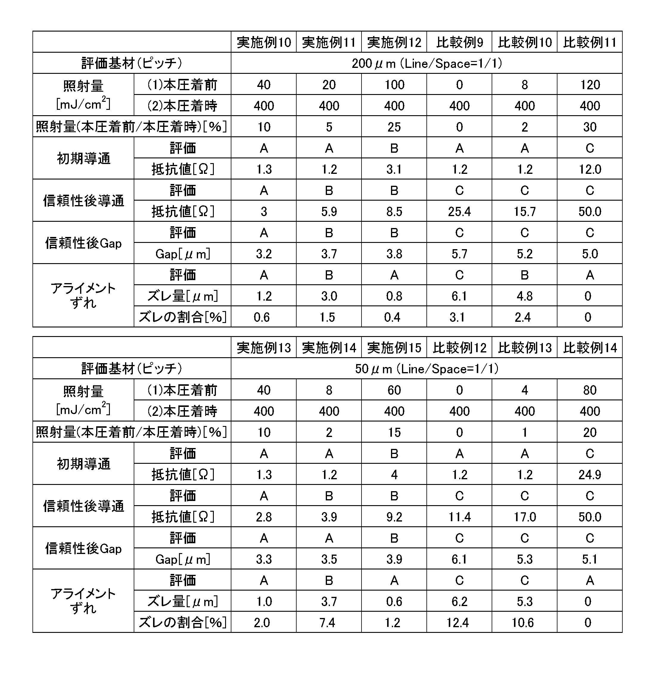
フレキシブル基板の最小配線間スペースが25μmを超える実施例10~12では、光照射工程における光の照射量を、本圧着工程における光の照射量の5~25%とした。これにより、初期導通抵抗値、信頼性試験後の導通抵抗値、信頼性試験後のギャップ、及びアライメントずれ量の評価がいずれも良好であることが分かった。
フレキシブル基板の最小配線間スペースが25μm以下である実施例13~15では、光照射工程における光の照射量を、本圧着工程における光の照射量の2~15%とした。これにより、初期導通抵抗値、信頼性試験後の導通抵抗値、信頼性試験後のギャップ、及びアライメントずれ量の評価がいずれも良好であることが分かった。
比較例9、12では、光照射工程において紫外線を照射しなかったため、本圧着工程における加熱押圧時に、信頼性試験後の導通抵抗値、信頼性試験後のギャップ、及びフレキシブル基板のアライメントずれの評価が良好ではないことが分かった。また、比較例10、13では、光照射工程における紫外線照射量が、本圧着工程における紫外線照射量に対して少なすぎたため、信頼性試験後の導通抵抗値、及び信頼性試験後のギャップの評価が良好ではないことが分かった。また、比較例13では、フレキシブル基板のアライメントずれの評価も良好ではないことが分かった。これらの結果は、本圧着工程における加熱押圧時に、異方性導電フィルムを構成するバインダー樹脂の流動性が大きくなりすぎてしまい、フレキシブル基板の配線間が撓んだ状態で加熱ツールのプレスアウト時にフレキシブル基板の残留応力が開放された際に、異方性導電フィルムとフレキシブル基板との界面における剥離が発生しやすくなってしまったためと考えられる。
比較例11、14では、光照射工程における紫外線照射量が、本圧着工程における紫外線照射量に対して多すぎたため、初期導通抵抗値、信頼性試験後の導通抵抗値、及び信頼性試験後のギャップの評価が良好ではないことが分かった。この結果は、異方性導電フィルムを構成するバインダー樹脂の硬化反応が進みすぎ、本圧着工程において導電性粒子を十分に押し込むことができなかたためと考えられる。
[実施例16~19]
実施例16~19では、実施例10、11、13,14と同様にクロム/アルミコーティングガラスに、異方性導電フィルムを貼付け、異方性導電フィルム側から、異方性導電フィルムの全面に対して紫外線を20mJ/cm2(本圧着時の5%)照射(先照射)した。この異方性導電フィルム側からの先照射は、透明基板側からの光照射と略同一の光源を用いた。紫外線照射後、異方性導電フィルム上にフレキシブル基板を位置合わせして積層体を得た。この積層体に対して、実施例10、11、13、14と同様の条件で光照射および本圧着を行った。実施例16~19では実施例10、11、13、14と略同等の結果が得られた。
実施例16~19では、実施例10、11、13,14と同様にクロム/アルミコーティングガラスに、異方性導電フィルムを貼付け、異方性導電フィルム側から、異方性導電フィルムの全面に対して紫外線を20mJ/cm2(本圧着時の5%)照射(先照射)した。この異方性導電フィルム側からの先照射は、透明基板側からの光照射と略同一の光源を用いた。紫外線照射後、異方性導電フィルム上にフレキシブル基板を位置合わせして積層体を得た。この積層体に対して、実施例10、11、13、14と同様の条件で光照射および本圧着を行った。実施例16~19では実施例10、11、13、14と略同等の結果が得られた。
[実施例20~29]
実施例20~29では、実施例10~19と同様にクロム/アルミコーティングガラスに、異方性導電フィルムを貼付け、仮圧着工程で透明基板側から光照射する際に、60℃、1MPaで押圧する以外は同等の操作を繰り返し、本圧着を行った。実施例20~29では実施例10~19と略同等の結果が得られた。
実施例20~29では、実施例10~19と同様にクロム/アルミコーティングガラスに、異方性導電フィルムを貼付け、仮圧着工程で透明基板側から光照射する際に、60℃、1MPaで押圧する以外は同等の操作を繰り返し、本圧着を行った。実施例20~29では実施例10~19と略同等の結果が得られた。
1 異方性導電フィルム、2 剥離フィルム、3 バインダー樹脂層、4 導電性粒子、10 液晶表示パネル、11,12 透明基板、13 シール、14 液晶、15 パネル表示部、16,17 透明電極、18 液晶駆動用IC、20 COG実装部、21 フレキシブル基板、22 FOG実装部、24 配厚膜、25,26 偏光板、30 加熱押圧ヘッド、31 紫外線照射器、42 バンプ、43 配線、44 ギャップ、45,46 端子
Claims (19)
- 光重合開始剤を含有する回路接続用接着剤を透明基板上に設ける接着剤配置工程と、
上記回路接続用接着剤を介して上記透明基板上に電子部品を配置し、上記回路接続用接着剤への光照射を行う光照射工程と、
上記電子部品を上記透明基板に対して押圧しながら、加熱及び光照射を行う本圧着工程とを有し、
上記光照射工程における光の照射量は、上記本圧着工程における光の照射量よりも小さい接続体の製造方法。 - 上記接着剤配置工程と上記光照射工程との間に、上記回路接続用接着剤側から、上記回路接続用接着剤全面に対して光照射を行う先照射工程をさらに有し、
上記先照射工程と上記光照射工程の合計の光照射量は、上記本圧着工程の光照射量よりも小さい、請求項1記載の接続体の製造方法。 - 上記光照射工程は、上記透明基板側から光照射を行う、請求項1又は2に記載の接続体の製造方法。
- 上記光照射工程では、上記電子部品の最小配線間スペースによって光の照射量を変更する、請求項1~3のいずれか1項に記載の接続体の製造方法。
- 上記光照射工程における光の照射時間は、上記本圧着工程における圧着時間に対して1/5以下である、請求項1~4のいずれか1項に記載の接続体の製造方法。
- 光重合開始剤を含有する回路接続用接着剤を透明基板上に設ける接着剤配置工程と、
上記回路接続用接着剤を介して上記透明基板上に電子部品を配置し、上記電子部品の上記透明基板への押圧、及び上記回路接続用接着剤への光照射を行う仮圧着工程と、
上記電子部品を上記透明基板に対して押圧しながら、加熱及び光照射を行う本圧着工程とを有し、
上記仮圧着工程における光の照射量は、上記本圧着工程における光の照射量よりも小さい接続体の製造方法。 - 上記接着剤配置工程と上記仮圧着工程との間に、上記回路接続用接着剤側から、上記回路接続用接着剤全面に対して光照射を行う先照射工程をさらに有し、
上記先照射工程と上記仮圧着工程の合計の光照射量は、上記本圧着工程の光照射量よりも小さい、請求項6記載の接続体の製造方法。 - 上記仮圧着工程は、上記透明基板側から光照射を行う、請求項6又は7に記載の接続体の製造方法。
- 上記仮圧着工程では、上記電子部品の最小配線間スペースによって光の照射量を変更する、請求項6~8のいずれか1項に記載の接続体の製造方法。
- 上記仮圧着工程における光の照射量は、上記本圧着工程における光の照射量の3~20%である請求項6~9のいずれか1項に記載の接続体の製造方法。
- 上記仮圧着工程における光の照度は、3~20mW/cm2である請求項10記載の接続体の製造方法。
- 上記仮圧着工程における光の照射時間は0.5~2秒である請求項10又は11に記載の接続体の製造方法。
- 上記仮圧着工程における上記電子部品への押圧力は、上記本圧着工程における上記電子部品への押圧力の40~90%である請求項6~12いずれか1項に記載の接続体の製造方法。
- 上記仮圧着工程は、圧着ツールが上記電子部品の押圧面に当接されたと同時に光照射を開始する請求項6~13のいずれか1項に記載の接続体の製造方法。
- 上記接着剤配置工程から上記回路接続用接着剤への光照射を行う請求項6~13のいずれか1項に記載の接続体の製造方法。
- 上記仮圧着工程における上記電子部品の圧着温度が、上記本圧着工程における上記電子部品の圧着温度と同等である請求項6~15のいずれか1項に記載の接続体の製造方法。
- 光重合開始剤を含有する回路接続用接着剤を透明基板上に設ける接着剤配置工程と、
上記回路接続用接着剤を介して上記透明基板上に電子部品を配置し、上記回路接続用接着剤への光照射を行う光照射工程と、
上記電子部品を上記透明基板に対して押圧しながら、加熱及び光照射を行う本圧着工程とを有し、
上記光照射工程における光の照射量は、上記本圧着工程における光の照射量よりも小さい電子部品の接続方法。 - 上記光照射工程は、上記回路接続用接着剤を介して上記透明基板上に電子部品を配置し、上記電子部品の上記透明基板への押圧、及び上記回路接続用接着剤への光照射を行う仮圧着工程である、請求項17に記載の電子部品の接続方法。
- 請求項1~16のいずれか1項に記載の方法により製造された接続体。
Priority Applications (2)
| Application Number | Priority Date | Filing Date | Title |
|---|---|---|---|
| CN201680005144.3A CN107078071B (zh) | 2015-01-20 | 2016-01-20 | 连接体的制造方法、电子部件的连接方法、连接体 |
| KR1020177010336A KR101969248B1 (ko) | 2015-01-20 | 2016-01-20 | 접속체의 제조 방법, 전자 부품의 접속 방법, 접속체 |
Applications Claiming Priority (4)
| Application Number | Priority Date | Filing Date | Title |
|---|---|---|---|
| JP2015-008950 | 2015-01-20 | ||
| JP2015008950 | 2015-01-20 | ||
| JP2016008718A JP6679320B2 (ja) | 2015-01-20 | 2016-01-20 | 接続体の製造方法、電子部品の接続方法 |
| JP2016-008718 | 2016-01-20 |
Publications (1)
| Publication Number | Publication Date |
|---|---|
| WO2016117613A1 true WO2016117613A1 (ja) | 2016-07-28 |
Family
ID=56417151
Family Applications (1)
| Application Number | Title | Priority Date | Filing Date |
|---|---|---|---|
| PCT/JP2016/051595 Ceased WO2016117613A1 (ja) | 2015-01-20 | 2016-01-20 | 接続体の製造方法、電子部品の接続方法、接続体 |
Country Status (1)
| Country | Link |
|---|---|
| WO (1) | WO2016117613A1 (ja) |
Citations (4)
| Publication number | Priority date | Publication date | Assignee | Title |
|---|---|---|---|---|
| JP2007045900A (ja) * | 2005-08-09 | 2007-02-22 | Hitachi Chem Co Ltd | 回路接続材料並びに回路端子の接続構造体及び接続方法 |
| JP2013058412A (ja) * | 2011-09-08 | 2013-03-28 | Sekisui Chem Co Ltd | 絶縁材料、積層体、接続構造体、積層体の製造方法及び接続構造体の製造方法 |
| JP2013105636A (ja) * | 2011-11-14 | 2013-05-30 | Dexerials Corp | 異方性導電フィルム、接続方法、及び接合体 |
| JP2014202821A (ja) * | 2013-04-02 | 2014-10-27 | 積水化学工業株式会社 | 液晶表示素子の製造方法及び接合材料 |
-
2016
- 2016-01-20 WO PCT/JP2016/051595 patent/WO2016117613A1/ja not_active Ceased
Patent Citations (4)
| Publication number | Priority date | Publication date | Assignee | Title |
|---|---|---|---|---|
| JP2007045900A (ja) * | 2005-08-09 | 2007-02-22 | Hitachi Chem Co Ltd | 回路接続材料並びに回路端子の接続構造体及び接続方法 |
| JP2013058412A (ja) * | 2011-09-08 | 2013-03-28 | Sekisui Chem Co Ltd | 絶縁材料、積層体、接続構造体、積層体の製造方法及び接続構造体の製造方法 |
| JP2013105636A (ja) * | 2011-11-14 | 2013-05-30 | Dexerials Corp | 異方性導電フィルム、接続方法、及び接合体 |
| JP2014202821A (ja) * | 2013-04-02 | 2014-10-27 | 積水化学工業株式会社 | 液晶表示素子の製造方法及び接合材料 |
Similar Documents
| Publication | Publication Date | Title |
|---|---|---|
| JP5972844B2 (ja) | 異方性導電フィルム、異方性導電フィルムの製造方法、接続体の製造方法、及び接続方法 | |
| TWI661027B (zh) | 連接體、連接體之製造方法、連接方法、異向性導電接著劑 | |
| KR102397500B1 (ko) | 이방성 도전 접착제, 접속체의 제조 방법 및 전자 부품의 접속 방법 | |
| WO2013129437A1 (ja) | 接続体の製造方法、及び異方性導電接着剤 | |
| TWI540591B (zh) | A connection method, a method of manufacturing a connector, and a linker | |
| JP6679320B2 (ja) | 接続体の製造方法、電子部品の接続方法 | |
| CN107001865B (zh) | 光固化类各向异性导电粘接剂、连接体的制造方法及电子部件的连接方法 | |
| JP5836830B2 (ja) | 接続体の製造方法、及び接続方法 | |
| TWI581972B (zh) | A method of manufacturing a connecting body, and a method of connecting an electronic component | |
| KR102665001B1 (ko) | 접속체의 제조 방법 | |
| JP6151412B2 (ja) | 異方性導電フィルム、異方性導電フィルムの製造方法、接続体の製造方法、及び接続方法 | |
| WO2016117613A1 (ja) | 接続体の製造方法、電子部品の接続方法、接続体 | |
| TWI603136B (zh) | Method of manufacturing connection body and connection method of electronic component | |
| HK1239947A1 (en) | Method for producing connected body, method for connecting electronic component, and connected body | |
| JP6393039B2 (ja) | 接続体の製造方法、接続方法及び接続体 | |
| WO2015111599A1 (ja) | 接続体の製造方法、電子部品の接続方法 | |
| HK1239947B (zh) | 连接体的制造方法、电子部件的连接方法、连接体 |
Legal Events
| Date | Code | Title | Description |
|---|---|---|---|
| 121 | Ep: the epo has been informed by wipo that ep was designated in this application |
Ref document number: 16740220 Country of ref document: EP Kind code of ref document: A1 |
|
| ENP | Entry into the national phase |
Ref document number: 20177010336 Country of ref document: KR Kind code of ref document: A |
|
| NENP | Non-entry into the national phase |
Ref country code: DE |
|
| 122 | Ep: pct application non-entry in european phase |
Ref document number: 16740220 Country of ref document: EP Kind code of ref document: A1 |