WO2016113797A1 - Semiconductor device and manufacturing method thereof - Google Patents
Semiconductor device and manufacturing method thereof Download PDFInfo
- Publication number
- WO2016113797A1 WO2016113797A1 PCT/JP2015/006178 JP2015006178W WO2016113797A1 WO 2016113797 A1 WO2016113797 A1 WO 2016113797A1 JP 2015006178 W JP2015006178 W JP 2015006178W WO 2016113797 A1 WO2016113797 A1 WO 2016113797A1
- Authority
- WO
- WIPO (PCT)
- Prior art keywords
- type
- semiconductor region
- trench
- type semiconductor
- bottom face
- Prior art date
- Legal status (The legal status is an assumption and is not a legal conclusion. Google has not performed a legal analysis and makes no representation as to the accuracy of the status listed.)
- Ceased
Links
Images





Classifications
-
- H—ELECTRICITY
- H10—SEMICONDUCTOR DEVICES; ELECTRIC SOLID-STATE DEVICES NOT OTHERWISE PROVIDED FOR
- H10D—INORGANIC ELECTRIC SEMICONDUCTOR DEVICES
- H10D62/00—Semiconductor bodies, or regions thereof, of devices having potential barriers
- H10D62/10—Shapes, relative sizes or dispositions of the regions of the semiconductor bodies; Shapes of the semiconductor bodies
- H10D62/102—Constructional design considerations for preventing surface leakage or controlling electric field concentration
- H10D62/103—Constructional design considerations for preventing surface leakage or controlling electric field concentration for increasing or controlling the breakdown voltage of reverse-biased devices
- H10D62/105—Constructional design considerations for preventing surface leakage or controlling electric field concentration for increasing or controlling the breakdown voltage of reverse-biased devices by having particular doping profiles, shapes or arrangements of PN junctions; by having supplementary regions, e.g. junction termination extension [JTE]
- H10D62/109—Reduced surface field [RESURF] PN junction structures
-
- H—ELECTRICITY
- H10—SEMICONDUCTOR DEVICES; ELECTRIC SOLID-STATE DEVICES NOT OTHERWISE PROVIDED FOR
- H10D—INORGANIC ELECTRIC SEMICONDUCTOR DEVICES
- H10D12/00—Bipolar devices controlled by the field effect, e.g. insulated-gate bipolar transistors [IGBT]
- H10D12/01—Manufacture or treatment
- H10D12/031—Manufacture or treatment of IGBTs
- H10D12/032—Manufacture or treatment of IGBTs of vertical IGBTs
- H10D12/038—Manufacture or treatment of IGBTs of vertical IGBTs having a recessed gate, e.g. trench-gate IGBTs
-
- H—ELECTRICITY
- H10—SEMICONDUCTOR DEVICES; ELECTRIC SOLID-STATE DEVICES NOT OTHERWISE PROVIDED FOR
- H10D—INORGANIC ELECTRIC SEMICONDUCTOR DEVICES
- H10D12/00—Bipolar devices controlled by the field effect, e.g. insulated-gate bipolar transistors [IGBT]
- H10D12/01—Manufacture or treatment
- H10D12/031—Manufacture or treatment of IGBTs
-
- H—ELECTRICITY
- H10—SEMICONDUCTOR DEVICES; ELECTRIC SOLID-STATE DEVICES NOT OTHERWISE PROVIDED FOR
- H10D—INORGANIC ELECTRIC SEMICONDUCTOR DEVICES
- H10D12/00—Bipolar devices controlled by the field effect, e.g. insulated-gate bipolar transistors [IGBT]
- H10D12/411—Insulated-gate bipolar transistors [IGBT]
- H10D12/441—Vertical IGBTs
- H10D12/461—Vertical IGBTs having non-planar surfaces, e.g. having trenches, recesses or pillars in the surfaces of the emitter, base or collector regions
- H10D12/481—Vertical IGBTs having non-planar surfaces, e.g. having trenches, recesses or pillars in the surfaces of the emitter, base or collector regions having gate structures on slanted surfaces, on vertical surfaces, or in grooves, e.g. trench gate IGBTs
-
- H—ELECTRICITY
- H10—SEMICONDUCTOR DEVICES; ELECTRIC SOLID-STATE DEVICES NOT OTHERWISE PROVIDED FOR
- H10D—INORGANIC ELECTRIC SEMICONDUCTOR DEVICES
- H10D30/00—Field-effect transistors [FET]
- H10D30/01—Manufacture or treatment
- H10D30/021—Manufacture or treatment of FETs having insulated gates [IGFET]
- H10D30/028—Manufacture or treatment of FETs having insulated gates [IGFET] of double-diffused metal oxide semiconductor [DMOS] FETs
- H10D30/0291—Manufacture or treatment of FETs having insulated gates [IGFET] of double-diffused metal oxide semiconductor [DMOS] FETs of vertical DMOS [VDMOS] FETs
- H10D30/0297—Manufacture or treatment of FETs having insulated gates [IGFET] of double-diffused metal oxide semiconductor [DMOS] FETs of vertical DMOS [VDMOS] FETs using recessing of the gate electrodes, e.g. to form trench gate electrodes
-
- H—ELECTRICITY
- H10—SEMICONDUCTOR DEVICES; ELECTRIC SOLID-STATE DEVICES NOT OTHERWISE PROVIDED FOR
- H10D—INORGANIC ELECTRIC SEMICONDUCTOR DEVICES
- H10D30/00—Field-effect transistors [FET]
- H10D30/60—Insulated-gate field-effect transistors [IGFET]
- H10D30/64—Double-diffused metal-oxide semiconductor [DMOS] FETs
- H10D30/66—Vertical DMOS [VDMOS] FETs
- H10D30/668—Vertical DMOS [VDMOS] FETs having trench gate electrodes, e.g. UMOS transistors
-
- H—ELECTRICITY
- H10—SEMICONDUCTOR DEVICES; ELECTRIC SOLID-STATE DEVICES NOT OTHERWISE PROVIDED FOR
- H10D—INORGANIC ELECTRIC SEMICONDUCTOR DEVICES
- H10D62/00—Semiconductor bodies, or regions thereof, of devices having potential barriers
- H10D62/10—Shapes, relative sizes or dispositions of the regions of the semiconductor bodies; Shapes of the semiconductor bodies
- H10D62/102—Constructional design considerations for preventing surface leakage or controlling electric field concentration
- H10D62/103—Constructional design considerations for preventing surface leakage or controlling electric field concentration for increasing or controlling the breakdown voltage of reverse-biased devices
- H10D62/105—Constructional design considerations for preventing surface leakage or controlling electric field concentration for increasing or controlling the breakdown voltage of reverse-biased devices by having particular doping profiles, shapes or arrangements of PN junctions; by having supplementary regions, e.g. junction termination extension [JTE]
- H10D62/106—Constructional design considerations for preventing surface leakage or controlling electric field concentration for increasing or controlling the breakdown voltage of reverse-biased devices by having particular doping profiles, shapes or arrangements of PN junctions; by having supplementary regions, e.g. junction termination extension [JTE] having supplementary regions doped oppositely to or in rectifying contact with regions of the semiconductor bodies, e.g. guard rings with PN or Schottky junctions
- H10D62/107—Buried supplementary regions, e.g. buried guard rings
-
- H—ELECTRICITY
- H10—SEMICONDUCTOR DEVICES; ELECTRIC SOLID-STATE DEVICES NOT OTHERWISE PROVIDED FOR
- H10D—INORGANIC ELECTRIC SEMICONDUCTOR DEVICES
- H10D62/00—Semiconductor bodies, or regions thereof, of devices having potential barriers
- H10D62/10—Shapes, relative sizes or dispositions of the regions of the semiconductor bodies; Shapes of the semiconductor bodies
- H10D62/17—Semiconductor regions connected to electrodes not carrying current to be rectified, amplified or switched, e.g. channel regions
- H10D62/393—Body regions of DMOS transistors or IGBTs
-
- H—ELECTRICITY
- H10—SEMICONDUCTOR DEVICES; ELECTRIC SOLID-STATE DEVICES NOT OTHERWISE PROVIDED FOR
- H10D—INORGANIC ELECTRIC SEMICONDUCTOR DEVICES
- H10D62/00—Semiconductor bodies, or regions thereof, of devices having potential barriers
- H10D62/80—Semiconductor bodies, or regions thereof, of devices having potential barriers characterised by the materials
- H10D62/83—Semiconductor bodies, or regions thereof, of devices having potential barriers characterised by the materials being Group IV materials, e.g. B-doped Si or undoped Ge
- H10D62/832—Semiconductor bodies, or regions thereof, of devices having potential barriers characterised by the materials being Group IV materials, e.g. B-doped Si or undoped Ge being Group IV materials comprising two or more elements, e.g. SiGe
- H10D62/8325—Silicon carbide
-
- H—ELECTRICITY
- H10—SEMICONDUCTOR DEVICES; ELECTRIC SOLID-STATE DEVICES NOT OTHERWISE PROVIDED FOR
- H10P—GENERIC PROCESSES OR APPARATUS FOR THE MANUFACTURE OR TREATMENT OF DEVICES COVERED BY CLASS H10
- H10P30/00—Ion implantation into wafers, substrates or parts of devices
- H10P30/20—Ion implantation into wafers, substrates or parts of devices into semiconductor materials, e.g. for doping
- H10P30/22—Ion implantation into wafers, substrates or parts of devices into semiconductor materials, e.g. for doping using masks
Definitions
- the technique disclosed in the present application relates to a semiconductor device comprising a p-type semiconductor region in contact with a bottom surface of a trench gate, and a method of manufacturing the same.
- Patent Literature 1 discloses a semiconductor device including a p-type semiconductor region in contact with a bottom face of a trench gate.
- the p-type semiconductor region relaxes an electric field applied to the bottom face of the trench gate and improves a withstand voltage of the semiconductor device.
- Patent Literature 1 Japanese Patent Application Publication No. 2006-128507
- a p-type semiconductor region is formed by forming a trench extending along a depth direction from one of main surfaces of a semiconductor layer, and then irradiating p-type impurities toward the trench.
- a protective film is formed on the side face of the trench. The p-type impurities are not introduced to an edge part of the bottom face of the trench, and introduced to a central part of the bottom face of the trench due to a thickness of the protective film.
- the p-type semiconductor region is not only formed under the edge of the bottom face of the trench gate, but also formed at a deeper position under the bottom face of the trench gate in order to relax an electric field applied to the bottom face of the trench gate.
- a p-type semiconductor region that satisfies these conditions is formed by thermal diffusion of a single type of p-type impurities having a relatively large diffusion coefficient.
- the p-type semiconductor region formed by such thermal diffusion spreads isotropically and hence spreads along a lateral direction unnecessarily at the deeper position under the bottom face of the trench gate, resulting in an increase in on-resistance of the semiconductor device.
- a configuration required for a p-type semiconductor region is preferably a configuration that the p-type semiconductor region spreads, at a shallower position under the bottom face of the trench gate, along the lateral direction so as to be located under the edge of the bottom face of the trench gate, whereas the p-type semiconductor region spreads, at the deeper position under the bottom face of the trench gate, along a depth direction, with its spreading along the lateral direction being suppressed, in other words, a T-shape configuration in cross section as a whole. It is, however, difficult for a p-type semiconductor region formed with a single type of p-type impurities having a relatively large diffusion coefficient, to have such configuration.
- the present specification provides a technique that improves both of a withstand voltage and an on-resistance in a semiconductor device that comprises a p-type semiconductor region in contact with a bottom face of a trench gate.
- a semiconductor device disclosed in the present specification comprises a trench gate and a p-type semiconductor region.
- the trench gate extends from one of main surfaces of a semiconductor layer along a depth direction.
- the p-type semiconductor region is in contact with a bottom face of the trench gate.
- the p-type semiconductor region includes a first p-type semiconductor region containing a first type of p-type impurities and a second p-type semiconductor region containing a second type of p-type impurities.
- the first p-type semiconductor region is located between the trench gate and the second p-type semiconductor region.
- the second p-type semiconductor region is located within a part of the first p-type semiconductor region.
- a diffusion coefficient of the second type of p-type impurities is smaller than a diffusion coefficient of the first type of p-type impurities.
- the p-type semiconductor region is formed with two types of p-type impurities having different diffusion coefficients.
- the first p-type semiconductor region that contains a first type of p-type impurities having a relatively large diffusion coefficient is formed at a shallower position under the bottom face of the trench, and the second p-type semiconductor region that contains the second type of p-type impurities having a relatively small diffusion coefficient is formed at a deeper position under the bottom face of the trench.
- the p-type semiconductor region can thereby have a configuration in which it spreads, at the shallower position under the bottom face of the trench, along a lateral direction, whereas it spreads, at the deeper position under the bottom face of the trench, along a depth direction with its spreading along the lateral direction being suppressed.
- the semiconductor device can have a feature of a high withstand voltage and a low on-resistance.
- a manufacturing method of a semiconductor device disclosed in the present specification comprises forming a mask, forming a trench, irradiating a first type of p-type impurities and irradiating a second type of p-type impurities.
- the mask is formed on one of main surfaces of a semiconductor layer, wherein an opening is formed in the mask.
- the trench is formed to extend along a depth direction from the one of main surfaces which is exposed at the opening of the mask.
- the first type of p-type impurities is irradiated through the opening and toward the trench.
- the second type of p-type impurities is irradiated through the opening and toward the trench.
- the second type of p-type impurities is introduced to a deeper position under a bottom face of the trench than the first type of p-type impurities.
- a diffusion coefficient of the second type of p-type impurities is smaller than a diffusion coefficient of the first type of p-type impurities.
- the first type of p-type impurities and the second type of p-type impurities are introduced under the bottom face of the trench, with the use of a common mask.
- This makes it possible to form a p-type semiconductor region that has the configuration in which it spreads, at a shallower position under the bottom face of the trench, along a lateral direction, whereas it spreads, at a deeper position under the bottom face of the trench, along a depth direction with its spreading along the lateral direction being suppressed.
- FIG. 1 schematically shows a cross section of a main part of a semiconductor device
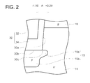
- FIG. 2 schematically shows an enlarged view of vicinity of an edge of a bottom face of a trench gate
- FIG. 3 shows a relation between spreading of a p-type semiconductor region along a lateral direction and a withstand voltage of the semiconductor device, and a relation between spreading of the p-type semiconductor region along the lateral direction and an on-resistance of the semiconductor device
- FIG. 4 shows a process of a manufacturing of a p-type semiconductor region in a manufacturing method of a semiconductor device
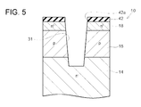
- FIG. 5 shows a process of the manufacturing of the p-type semiconductor region in the manufacturing method of the semiconductor device
- FIG. 1 schematically shows a cross section of a main part of a semiconductor device
- FIG. 2 schematically shows an enlarged view of vicinity of an edge of a bottom face of a trench gate
- FIG. 3 shows a relation between spreading of a p-type semiconductor region along a lateral direction and a
- FIG. 6 shows a process of the manufacturing of the p-type semiconductor region in the manufacturing method of the semiconductor device
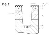
- FIG. 7 shows a process of the manufacturing of the p-type semiconductor region in the manufacturing method of the semiconductor device
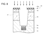
- FIG. 8 shows a process of the manufacturing of the p-type semiconductor region in the manufacturing method of the semiconductor device
- FIG. 9 shows a process of the manufacturing of the p-type semiconductor region in the manufacturing method of the semiconductor device.
- a semiconductor device 1 comprises a semiconductor layer 10 made of silicon carbide, a drain electrode 22 that covers a rear surface of the semiconductor layer 10, a source electrode 24 that covers a front surface of the semiconductor layer 10, and a trench gate 30 provided at a front layer part of the semiconductor layer 10.
- the trench gate 30 extends from the front surface of the semiconductor layer 10 along a depth direction (a direction orthogonal to the front surface of the semiconductor layer 10, i.e., a direction from a top to a bottom on the paper).
- FIG. 1 shows only one trench gate 30, the semiconductor layer 10 is provided with a plurality of trench gates 30.
- each trench gate 30 includes a gate electrode 32 and a gate insulating film 34.
- the gate insulating film 34 covers the gate electrode 32.
- the semiconductor layer 10 includes an n + -type drain region 12, an n - -type drift region 14, a p-type semiconductor region 15, a p-type body region 16, and an n + -type source region 18.
- the drain region 12 is provided at a rear layer part of the semiconductor layer 10, and is in ohmic contact with the drain electrode 22.
- the drift region 14 is provided between the drain region 12 and the body region 16, and is in contact with a side face 30a of the trench gate 30.
- the drift region 14 is a remaining part that is obtained after other semiconductor regions are formed in the semiconductor layer 10.
- the p-type semiconductor region 15 is in contact with a bottom face 30b of the trench gate 30.
- the p-type semiconductor region 15 in this example is separated from the body region 16 by the drift region 14, and has a floating potential.
- a p-type semiconductor region 15 may be configured to be in contact with a body region 16.
- the body region 16 is provided at the front layer part of the semiconductor layer 10, is provided between the drift region 14 and the source region 18, and is in contact with the side face 30a of the trench gate 30.
- the body region 16 is electrically connected to the source electrode 24 via a p + -type body contact region provided at a part of the cross section not shown.
- the source region 18 is provided at the front layer part of the semiconductor layer 10, is in contact with the side face 30a of the trench gate 30, and is in ohmic contact with the source electrode 24.
- a semiconductor structure that configures a MOSFET is provided in the semiconductor layer 10.
- the p-type semiconductor region 15 includes a first p-type semiconductor region 15a and a second p-type semiconductor region 15b.
- the first p-type semiconductor region 15a is in contact with the bottom face 30b of the trench gate 30, and is provided at a shallower position under the bottom face 30b of the trench gate 30.
- the first p-type semiconductor region 15a has a width larger than a width of the second p-type semiconductor region 15b, along a width direction of the trench gate 30 (a direction connecting portions of side face 30a that face each other, hereinafter also referred to as a lateral direction).
- the second p-type semiconductor region 15b is in contact with the first p-type semiconductor region 15a, and is provided at a deeper position under the bottom face 30b of the trench gate 30.
- the first p-type semiconductor region 15a has boron introduced thereto as p-type impurities
- the second p-type semiconductor region 15b has aluminum introduced thereto as p-type impurities.
- boron has a diffusion coefficient larger than a diffusion coefficient of aluminum.
- the first p-type semiconductor region 15a preferably contains boron at a concentration of at least equal to or more than 1 x 10 16 cm -3 , and in an example, the first p-type semiconductor region 15a is defined as containing boron at a concentration ranging from 1 x 10 16 to 1 x 10 18 cm -3 .
- the second p-type semiconductor region 15b preferably contains aluminum at a concentration of at least equal to or more than 1 x 10 16 cm -3 , and in an example, the second p-type semiconductor region 15b is defined as containing aluminum at a concentration ranging from 1 x 10 16 to 1 x 10 18 cm -3 .
- the first p-type semiconductor region 15a is also located under an edge 30c of the bottom face 30b of the trench gate 30, and projects out in a lateral direction from the edge 30c of the bottom face 30b of the trench gate 30.
- the second p-type semiconductor region 15b is located within a part of the first p-type semiconductor region 15a, in a view along the depth direction of the semiconductor layer 10.
- the second p-type semiconductor region 15b is located within a part of the bottom face 30b of the trench gate 30, in the view along the depth direction of the semiconductor layer 10.
- the p-type semiconductor region 15 has a configuration in which it spreads, at the shallower position under the bottom face 30b of the trench gate 30, along the lateral direction so as to be located under the edge 30c of the bottom face 30b of the trench gate 30, whereas it spreads, at the deeper position under the bottom face 30b of the trench gate 30, along the depth direction with its spreading along the lateral direction being suppressed, in other words, a T-shape configuration in cross section as a whole.
- FIGS. 2 and 3 show how the spreading of the first p-type semiconductor region 15a along the lateral direction affects a withstand voltage and an on-resistance of the semiconductor device 1.
- a distance along the width direction of the trench gate 30 is set as X
- an orientation in which the first p-type semiconductor region 15a projects out along the lateral direction from the edge 30c of the bottom face 30b of the trench gate 30 is set positive, and a reverse orientation thereof is set negative.
- the withstand voltage of the semiconductor device 1 is maintained high, and the on-resistance of the semiconductor device 1 is maintained low.
- the semiconductor device 1 can have superior characteristics in both the withstand voltage and the on-resistance.
- the first p-type semiconductor region 15a is not in contact with the side face 30a of the trench gate 30.
- the side face 30a of the trench gate 30 is a part where a channel is formed when the semiconductor device 1 is on.
- the semiconductor device 1 includes the p-type semiconductor region 15, the p-type semiconductor region 15 does not exist at this part where the channel is formed, resulting in that an increase in on-resistance is suppressed.
- the second p-type semiconductor region 15b has a width, along the lateral direction, smaller than the width of the first p-type semiconductor region 15a.
- the p-type semiconductor region in the conventional techniques is formed by isotropic thermal diffusion, and hence has a configuration of being spread widely along the lateral direction at a depth corresponding to a depth of the second p-type semiconductor region 15b.
- a current path of a current flowing in the drift region becomes narrow, resulting in an increase in on-resistance.
- the spreading of the second p-type semiconductor region 15b along the lateral direction has been suppressed, and hence a wide current path of the current flowing in the drift region 14 is ensured, resulting in a low on-resistance.
- the second p-type semiconductor region 15b has a configuration of being spread along the depth direction, resulting in that the withstand voltage of the semiconductor device 1 is maintained high.
- a manufacturing process of forming a p-type semiconductor region 15 in a manufacturing method of a semiconductor device 1 will now be described.
- known manufacturing steps can be utilized to manufacture the semiconductor device 1.
- a semiconductor layer 10 made of silicon carbide is prepared.
- a body region 16 and a source region 18 have been formed at a front layer part of the semiconductor layer 10.
- a TEOS film 42 is deposited on a front surface of the semiconductor layer 10 with the use of a CVD.
- the TEOS film 42 has a thickness of approximately 1.5 mm. Note that the TEOS film 42 is an example of a mask according to the appended claims.
- an opening 42a is formed in the TEOS film 42 to expose the front surface of the semiconductor layer 10.
- a trench 31 that extends along a depth direction from the front surface of the semiconductor layer 10, the front surface being exposed at the opening 42a of the TEOS film 42, is formed with the use of a dry-etching technique.
- the trench 31 has a side face inclined relative to the depth direction, and has a tapered shape in cross section. The trench 31 penetrates the source region 18 and the body region 16 to reach the drift region 14.
- boron ions 5a are irradiated toward the trench 31 through the opening 42a of the TEOS film 42 with the use of an ion implantation technique.
- the boron ions 5a have a low implantation energy of 60 to 240 keV, and are irradiated in a dose of 2.0 to 2.5 x 10 15 cm -2 .
- the boron ions 5a are irradiated in a multistage manner under the bottom face of the trench 31, so as to have a depth of equal to or smaller than 0.4 mm. At this time, the boron ions 5a are also introduced to the side face of the trench 31.
- a part of the side and bottom faces of the trench 31 is cut with the use of a chemical dry-etching.
- a thickness to be cut is approximately 60 nm.
- Most or all of a part of the side face of the trench 31 where the boron ions have been introduced is thereby removed by cutting.
- a concentration of the p-type impurities in the side face of the trench 31 is lowered to a concentration (5.0 x 10 15 cm -3 ) that provides a desired threshold voltage when compared to the concentration before the etching.
- aluminum ions 5b are irradiated toward the trench 31 through the opening 42a of the TEOS film 42 with the use of an ion implantation.
- the aluminum ions 5b have a high implantation energy of 240 to 900 keV, and are irradiated in a dose of 2.0 to 2.5 x 10 13 cm -2 .
- the aluminum ions 5b are irradiated in a multistage manner, so as to have a depth ranging from 0.3 to 0.8 mm under the bottom face of the trench 31. Due to the cutting, the side face of the trench 31 is located at a position retracted from a plane that defines the opening 42a of the TEOS film 42.
- the side face of the trench 31 is therefore shielded by the TEOS film 42, in a view along a direction along which the aluminum ions 5b are irradiated. Accordingly, the aluminum ions 5b are not introduced to the side face of the trench 31, and selectively introduced to the bottom face of the trench 31.
- activation annealing is performed after the TEOS film 42 is removed, so as to activate the boron ions 5a and the aluminum ions 5b having been introduced.
- a region where the boron ions 5a are activated serves as a first p-type semiconductor region 15a, whereas a region where the aluminum ions 5b are activated serves as a second p-type semiconductor region 15b, and a p-type semiconductor region 15 is thereby formed.
- the boron ions 5a have a large diffusion coefficient, and are thermally diffused by approximately 0.2 mm.
- the aluminum ions 5b have a small diffusion coefficient, and are hardly diffused. This allows the p-type semiconductor region 15 to have a T-shape configuration in cross section.
- boron ions of which diffusion coefficient is large only need to be introduced to a shallower position under the bottom face of the trench 31.
- the above-described manufacturing method it is not necessary to cause the boron ions to be thermally diffused unnecessarily, and hence the activation annealing can be controlled such that the boron ions do not come into contact with the side face 30a of the trench gate 30.
- the above-described manufacturing method can thereby provide a semiconductor device in which an increase in on-resistance is suppressed.
- the technique disclosed in the present specification may be applied to various kinds of semiconductor devices comprising a trench gate.
- the technique disclosed in the present specification may be applied to a MOSFET or an IGBT.
- One embodiment of a semiconductor device disclosed in the present specification may comprise a trench gate and a p-type semiconductor region.
- the trench gate may extend from one of main surfaces of a semiconductor layer along a depth direction.
- a configuration of the trench gate may not be especially limited, and a layout of the trench gate may not be especially limited.
- the p-type semiconductor region may be in contact with a bottom face of the trench gate.
- the p-type semiconductor region may include a first p-type semiconductor region containing a first type of p-type impurities and a second p-type semiconductor region containing a second type of p-type impurities.
- the first p-type semiconductor region may be located between the trench gate and the second p-type semiconductor region.
- An additional semiconductor region may be provided between the first p-type semiconductor region and the bottom face of the trench gate and/or between the first p-type semiconductor region and the second p-type semiconductor region.
- the second p-type semiconductor region may be located within a part of the first p-type semiconductor region.
- a diffusion coefficient of the second type of p-type impurities may be smaller than a diffusion coefficient of the first type of p-type impurities.
- the first p-type semiconductor region may be in contact with the bottom face of the trench gate, and may project out along a lateral direction from an edge of the bottom face of the trench gate.
- an electric field at the edge of the bottom face of the trench gate is relaxed, and a withstand voltage of the semiconductor device is accordingly improved.
- it is preferable that a length by which the first p-type semiconductor region projects out along the lateral direction from the edge of the bottom face of the trench gate is equal to or smaller than 0.2 mm. In this embodiment, even if a p-type semiconductor region is provided, an increase in on-resistance of the semiconductor device is suppressed.
- the first p-type semiconductor region is not in contact with a side face of the trench gate. In this embodiment also, even if a p-type semiconductor region is provided, an increase in on-resistance of the semiconductor device is suppressed.
- the second p-type semiconductor region may be located within a part of the trench gate.
- the second p-type semiconductor region may be located within a part of the trench gate.
- spreading of the second p-type semiconductor region along the lateral direction is suppressed. Therefore, even if a p-type semiconductor region is provided, a wide current path is ensured and an increase in on-resistance of the semiconductor device is suppressed.
- a manufacturing method of a semiconductor device disclosed in the present specification may comprise forming a mask, forming a trench, irradiating a first type of p-type impurities, and irradiating a second type of p-type impurities.
- the mask is formed on one of main surfaces of a semiconductor layer, wherein an opening is formed in the mask.
- the trench is formed to extend along a depth direction from the one of main surfaces which is exposed at the opening of the mask.
- the first type of p-type impurities is irradiated through the opening and toward the trench.
- the second type of p-type impurities is irradiated through the opening and toward the trench.
- a performing order in which the irradiating of the first type of p-type impurities and the irradiating of the second type of p-type impurities are performed earlier or later, may not be especially limited.
- the second type of p-type impurities is introduced to a deeper position under a bottom face of the trench than the first type of p-type impurities.
- a diffusion coefficient of the second type of p-type impurities is smaller than a diffusion coefficient of the first type of p-type impurities.
- the irradiating of the first type of p-type impurities may be performed prior to the irradiating of the second type of p-type impurities.
- the manufacturing method of the semiconductor device may further comprise removing side and bottom faces of the trench, in a state where the mask is maintained, so as to maintain the first type of p-type impurities having been introduced under the bottom face of the trench, wherein the removing is performed between the irradiating of the first type of p-type impurities and the irradiating of the second type of p-type impurities.
- the side face of the trench is shield by the mask so that the second type of p-type impurities is prevented from being irradiated to the side face of the trench.
Landscapes
- Electrodes Of Semiconductors (AREA)
Abstract
A semiconductor device includes a p-type semiconductor region in contact with a bottom face of a trench gate, wherein the p-type semiconductor region includes a first p-type semiconductor region containing a first type of p-type impurities and a second p-type semiconductor region containing a second type of p-type impurities. The first p-type semiconductor region is located between the trench gate and the second p-type semiconductor region. In a view along the depth direction, the second p-type semiconductor region is located within a part of the first p-type semiconductor region. A diffusion coefficient of the second type of p-type impurities is smaller than a diffusion coefficient of the first type of p-type impurities.
Description
This application claims priority to Japanese Patent Application No. 2015-005471 filed on January 15, 2015, the contents of which are hereby incorporated by reference into the present application.
The technique disclosed in the present application relates to a semiconductor device comprising a p-type semiconductor region in contact with a bottom surface of a trench gate, and a method of manufacturing the same.
[Patent Literature 1] Japanese Patent Application Publication No. 2006-128507
In conventional techniques, a p-type semiconductor region is formed by forming a trench extending along a depth direction from one of main surfaces of a semiconductor layer, and then irradiating p-type impurities toward the trench. In order to prevent the p-type impurities from being introduced to a side face of the trench when the p-type impurities are irradiated toward the trench, a protective film is formed on the side face of the trench. The p-type impurities are not introduced to an edge part of the bottom face of the trench, and introduced to a central part of the bottom face of the trench due to a thickness of the protective film.
It is preferable that the p-type semiconductor region is not only formed under the edge of the bottom face of the trench gate, but also formed at a deeper position under the bottom face of the trench gate in order to relax an electric field applied to the bottom face of the trench gate.
In the conventional techniques, a p-type semiconductor region that satisfies these conditions is formed by thermal diffusion of a single type of p-type impurities having a relatively large diffusion coefficient. The p-type semiconductor region formed by such thermal diffusion, however, spreads isotropically and hence spreads along a lateral direction unnecessarily at the deeper position under the bottom face of the trench gate, resulting in an increase in on-resistance of the semiconductor device.
As described above, a configuration required for a p-type semiconductor region is preferably a configuration that the p-type semiconductor region spreads, at a shallower position under the bottom face of the trench gate, along the lateral direction so as to be located under the edge of the bottom face of the trench gate, whereas the p-type semiconductor region spreads, at the deeper position under the bottom face of the trench gate, along a depth direction, with its spreading along the lateral direction being suppressed, in other words, a T-shape configuration in cross section as a whole. It is, however, difficult for a p-type semiconductor region formed with a single type of p-type impurities having a relatively large diffusion coefficient, to have such configuration.
The present specification provides a technique that improves both of a withstand voltage and an on-resistance in a semiconductor device that comprises a p-type semiconductor region in contact with a bottom face of a trench gate.
A semiconductor device disclosed in the present specification comprises a trench gate and a p-type semiconductor region. The trench gate extends from one of main surfaces of a semiconductor layer along a depth direction. The p-type semiconductor region is in contact with a bottom face of the trench gate. The p-type semiconductor region includes a first p-type semiconductor region containing a first type of p-type impurities and a second p-type semiconductor region containing a second type of p-type impurities. The first p-type semiconductor region is located between the trench gate and the second p-type semiconductor region. In a view along the depth direction, the second p-type semiconductor region is located within a part of the first p-type semiconductor region. A diffusion coefficient of the second type of p-type impurities is smaller than a diffusion coefficient of the first type of p-type impurities.
In the above-described semiconductor device, the p-type semiconductor region is formed with two types of p-type impurities having different diffusion coefficients. The first p-type semiconductor region that contains a first type of p-type impurities having a relatively large diffusion coefficient is formed at a shallower position under the bottom face of the trench, and the second p-type semiconductor region that contains the second type of p-type impurities having a relatively small diffusion coefficient is formed at a deeper position under the bottom face of the trench. The p-type semiconductor region can thereby have a configuration in which it spreads, at the shallower position under the bottom face of the trench, along a lateral direction, whereas it spreads, at the deeper position under the bottom face of the trench, along a depth direction with its spreading along the lateral direction being suppressed. The semiconductor device can have a feature of a high withstand voltage and a low on-resistance.
A manufacturing method of a semiconductor device disclosed in the present specification comprises forming a mask, forming a trench, irradiating a first type of p-type impurities and irradiating a second type of p-type impurities. In the forming of the mask, the mask is formed on one of main surfaces of a semiconductor layer, wherein an opening is formed in the mask. In the forming of the trench, the trench is formed to extend along a depth direction from the one of main surfaces which is exposed at the opening of the mask. In the irradiating of the first type of p-type impurities, the first type of p-type impurities is irradiated through the opening and toward the trench. In the irradiating of the second type of p-type impurities, the second type of p-type impurities is irradiated through the opening and toward the trench. The second type of p-type impurities is introduced to a deeper position under a bottom face of the trench than the first type of p-type impurities. A diffusion coefficient of the second type of p-type impurities is smaller than a diffusion coefficient of the first type of p-type impurities.
According to the above-described manufacturing method, the first type of p-type impurities and the second type of p-type impurities are introduced under the bottom face of the trench, with the use of a common mask. This makes it possible to form a p-type semiconductor region that has the configuration in which it spreads, at a shallower position under the bottom face of the trench, along a lateral direction, whereas it spreads, at a deeper position under the bottom face of the trench, along a depth direction with its spreading along the lateral direction being suppressed. According to the above-described manufacturing method, it is therefore possible to manufacture a semiconductor device that comprises a p-type semiconductor region having such configuration.
As shown in FIG. 1, a semiconductor device 1 comprises a semiconductor layer 10 made of silicon carbide, a drain electrode 22 that covers a rear surface of the semiconductor layer 10, a source electrode 24 that covers a front surface of the semiconductor layer 10, and a trench gate 30 provided at a front layer part of the semiconductor layer 10. The trench gate 30 extends from the front surface of the semiconductor layer 10 along a depth direction (a direction orthogonal to the front surface of the semiconductor layer 10, i.e., a direction from a top to a bottom on the paper). Although FIG. 1 shows only one trench gate 30, the semiconductor layer 10 is provided with a plurality of trench gates 30. In a view along the depth direction of the semiconductor layer 10 (in a planar view of the semiconductor layer 10), the plurality of trench gates 30 may be arranged in a stripe-shaped manner, or may be interspersed like islands. Each trench gate 30 includes a gate electrode 32 and a gate insulating film 34. The gate insulating film 34 covers the gate electrode 32.
The semiconductor layer 10 includes an n+-type drain region 12, an n--type drift region 14, a p-type semiconductor region 15, a p-type body region 16, and an n+-type source region 18. The drain region 12 is provided at a rear layer part of the semiconductor layer 10, and is in ohmic contact with the drain electrode 22. The drift region 14 is provided between the drain region 12 and the body region 16, and is in contact with a side face 30a of the trench gate 30. The drift region 14 is a remaining part that is obtained after other semiconductor regions are formed in the semiconductor layer 10. The p-type semiconductor region 15 is in contact with a bottom face 30b of the trench gate 30. The p-type semiconductor region 15 in this example is separated from the body region 16 by the drift region 14, and has a floating potential. As an alternative to this example, a p-type semiconductor region 15 may be configured to be in contact with a body region 16. The body region 16 is provided at the front layer part of the semiconductor layer 10, is provided between the drift region 14 and the source region 18, and is in contact with the side face 30a of the trench gate 30. The body region 16 is electrically connected to the source electrode 24 via a p+-type body contact region provided at a part of the cross section not shown. The source region 18 is provided at the front layer part of the semiconductor layer 10, is in contact with the side face 30a of the trench gate 30, and is in ohmic contact with the source electrode 24. As such, a semiconductor structure that configures a MOSFET is provided in the semiconductor layer 10.
The p-type semiconductor region 15 includes a first p-type semiconductor region 15a and a second p-type semiconductor region 15b. The first p-type semiconductor region 15a is in contact with the bottom face 30b of the trench gate 30, and is provided at a shallower position under the bottom face 30b of the trench gate 30. The first p-type semiconductor region 15a has a width larger than a width of the second p-type semiconductor region 15b, along a width direction of the trench gate 30 (a direction connecting portions of side face 30a that face each other, hereinafter also referred to as a lateral direction). The second p-type semiconductor region 15b is in contact with the first p-type semiconductor region 15a, and is provided at a deeper position under the bottom face 30b of the trench gate 30. The first p-type semiconductor region 15a has boron introduced thereto as p-type impurities, and the second p-type semiconductor region 15b has aluminum introduced thereto as p-type impurities. In silicon carbide, boron has a diffusion coefficient larger than a diffusion coefficient of aluminum. Note that the first p-type semiconductor region 15a preferably contains boron at a concentration of at least equal to or more than 1 x 1016 cm-3, and in an example, the first p-type semiconductor region 15a is defined as containing boron at a concentration ranging from 1 x 10¹⁶ to 1 x 1018 cm-3. Similarly, the second p-type semiconductor region 15b preferably contains aluminum at a concentration of at least equal to or more than 1 x 1016 cm-3, and in an example, the second p-type semiconductor region 15b is defined as containing aluminum at a concentration ranging from 1 x 10¹⁶ to 1 x 1018 cm-3.
The first p-type semiconductor region 15a is also located under an edge 30c of the bottom face 30b of the trench gate 30, and projects out in a lateral direction from the edge 30c of the bottom face 30b of the trench gate 30. The second p-type semiconductor region 15b is located within a part of the first p-type semiconductor region 15a, in a view along the depth direction of the semiconductor layer 10. Moreover, the second p-type semiconductor region 15b is located within a part of the bottom face 30b of the trench gate 30, in the view along the depth direction of the semiconductor layer 10. As such, the p-type semiconductor region 15 has a configuration in which it spreads, at the shallower position under the bottom face 30b of the trench gate 30, along the lateral direction so as to be located under the edge 30c of the bottom face 30b of the trench gate 30, whereas it spreads, at the deeper position under the bottom face 30b of the trench gate 30, along the depth direction with its spreading along the lateral direction being suppressed, in other words, a T-shape configuration in cross section as a whole.
FIGS. 2 and 3 show how the spreading of the first p-type semiconductor region 15a along the lateral direction affects a withstand voltage and an on-resistance of the semiconductor device 1. When the edge 30c of the bottom face 30b of the trench gate 30 is set as a reference A, a distance along the width direction of the trench gate 30 is set as X, and an orientation in which the first p-type semiconductor region 15a projects out along the lateral direction from the edge 30c of the bottom face 30b of the trench gate 30 is set positive, and a reverse orientation thereof is set negative. As shown in FIG. 3, in a range from -0.15 mm to +0.20 mm with respect to the reference A, the withstand voltage of the semiconductor device 1 is maintained high, and the on-resistance of the semiconductor device 1 is maintained low. In particular, in a case where the orientation is positive with respect to the reference A and the distance is equal to or smaller than 0.20 mm, in other words, in a case where the first p-type semiconductor region 15a projects out along the lateral direction from the edge 30c of the bottom face 30b of the trench gate 30 and a length by which the first p-type semiconductor region 15a projects out is equal to or smaller than 0.20 mm, the semiconductor device 1 can have superior characteristics in both the withstand voltage and the on-resistance.
In addition, the first p-type semiconductor region 15a is not in contact with the side face 30a of the trench gate 30. The side face 30a of the trench gate 30 is a part where a channel is formed when the semiconductor device 1 is on. Although the semiconductor device 1 includes the p-type semiconductor region 15, the p-type semiconductor region 15 does not exist at this part where the channel is formed, resulting in that an increase in on-resistance is suppressed.
The second p-type semiconductor region 15b has a width, along the lateral direction, smaller than the width of the first p-type semiconductor region 15a. For example, the p-type semiconductor region in the conventional techniques is formed by isotropic thermal diffusion, and hence has a configuration of being spread widely along the lateral direction at a depth corresponding to a depth of the second p-type semiconductor region 15b. Thus in the conventional semiconductor device, a current path of a current flowing in the drift region becomes narrow, resulting in an increase in on-resistance. On the other hand, in the semiconductor device 1, the spreading of the second p-type semiconductor region 15b along the lateral direction has been suppressed, and hence a wide current path of the current flowing in the drift region 14 is ensured, resulting in a low on-resistance. Moreover, the second p-type semiconductor region 15b has a configuration of being spread along the depth direction, resulting in that the withstand voltage of the semiconductor device 1 is maintained high.
A manufacturing process of forming a p-type semiconductor region 15 in a manufacturing method of a semiconductor device 1 will now be described. As for manufacturing processes other than the process of forming the p-type semiconductor region 15, known manufacturing steps can be utilized to manufacture the semiconductor device 1.
Initially, as shown in FIG. 4, a semiconductor layer 10 made of silicon carbide is prepared. A body region 16 and a source region 18 have been formed at a front layer part of the semiconductor layer 10.
Next, as shown in FIG. 5, a TEOS film 42 is deposited on a front surface of the semiconductor layer 10 with the use of a CVD. The TEOS film 42 has a thickness of approximately 1.5 mm. Note that the TEOS film 42 is an example of a mask according to the appended claims. Next, an opening 42a is formed in the TEOS film 42 to expose the front surface of the semiconductor layer 10. Next, a trench 31 that extends along a depth direction from the front surface of the semiconductor layer 10, the front surface being exposed at the opening 42a of the TEOS film 42, is formed with the use of a dry-etching technique. The trench 31 has a side face inclined relative to the depth direction, and has a tapered shape in cross section. The trench 31 penetrates the source region 18 and the body region 16 to reach the drift region 14.
Next, as shown in FIG. 6, boron ions 5a are irradiated toward the trench 31 through the opening 42a of the TEOS film 42 with the use of an ion implantation technique. The boron ions 5a have a low implantation energy of 60 to 240 keV, and are irradiated in a dose of 2.0 to 2.5 x 1015 cm-2. The boron ions 5a are irradiated in a multistage manner under the bottom face of the trench 31, so as to have a depth of equal to or smaller than 0.4 mm. At this time, the boron ions 5a are also introduced to the side face of the trench 31.
Next, as shown in FIG. 7, a part of the side and bottom faces of the trench 31 is cut with the use of a chemical dry-etching. A thickness to be cut is approximately 60 nm. Most or all of a part of the side face of the trench 31 where the boron ions have been introduced is thereby removed by cutting. As for the bottom face of the trench 31, most of a part where the boron ions have been introduced remains as it is. A concentration of the p-type impurities in the side face of the trench 31 is lowered to a concentration (5.0 x 1015 cm-3) that provides a desired threshold voltage when compared to the concentration before the etching.
Next, as shown in FIG. 8, aluminum ions 5b are irradiated toward the trench 31 through the opening 42a of the TEOS film 42 with the use of an ion implantation. The aluminum ions 5b have a high implantation energy of 240 to 900 keV, and are irradiated in a dose of 2.0 to 2.5 x 1013 cm-2. The aluminum ions 5b are irradiated in a multistage manner, so as to have a depth ranging from 0.3 to 0.8 mm under the bottom face of the trench 31. Due to the cutting, the side face of the trench 31 is located at a position retracted from a plane that defines the opening 42a of the TEOS film 42. The side face of the trench 31 is therefore shielded by the TEOS film 42, in a view along a direction along which the aluminum ions 5b are irradiated. Accordingly, the aluminum ions 5b are not introduced to the side face of the trench 31, and selectively introduced to the bottom face of the trench 31.
Next, as shown in FIG. 9, activation annealing is performed after the TEOS film 42 is removed, so as to activate the boron ions 5a and the aluminum ions 5b having been introduced. A region where the boron ions 5a are activated serves as a first p-type semiconductor region 15a, whereas a region where the aluminum ions 5b are activated serves as a second p-type semiconductor region 15b, and a p-type semiconductor region 15 is thereby formed. At this time, the boron ions 5a have a large diffusion coefficient, and are thermally diffused by approximately 0.2 mm. On the other hand, the aluminum ions 5b have a small diffusion coefficient, and are hardly diffused. This allows the p-type semiconductor region 15 to have a T-shape configuration in cross section.
In the above-described manufacturing method, aluminum ions, which have a small diffusion coefficient, are introduced at a deeper position under the bottom face of the trench 31. This makes it possible to form the second p-type semiconductor region 15b at the deeper position under the bottom face of the trench 31, and hence it is not necessary to cause boron ions of which diffusion coefficient is large, to be thermally diffused widely along the depth direction. For example, in the conventional manufacturing method, it is necessary to cause boron ions of which diffusion coefficient is large, to be thermally diffused widely along the depth direction, resulting in that the boron ions are thermally diffused widely along the lateral direction unnecessarily. On the other hand, in the above-described manufacturing method, boron ions of which diffusion coefficient is large, only need to be introduced to a shallower position under the bottom face of the trench 31. In the above-described manufacturing method, it is possible to cause the boron ions, which have been introduced to the shallower position under the bottom face of the trench 31, to be thermally diffused at a desired position under the edge of the bottom face of the trench 31, without causing them to be thermally diffused widely along the depth direction. In addition, in the above-described manufacturing method, it is not necessary to cause the boron ions to be thermally diffused unnecessarily, and hence the activation annealing can be controlled such that the boron ions do not come into contact with the side face 30a of the trench gate 30. The above-described manufacturing method can thereby provide a semiconductor device in which an increase in on-resistance is suppressed.
Some advantages of the technique disclosed in the present specification are summarized below. Matters described below have independently technical usefulness.
The technique disclosed in the present specification may be applied to various kinds of semiconductor devices comprising a trench gate. For example, the technique disclosed in the present specification may be applied to a MOSFET or an IGBT. One embodiment of a semiconductor device disclosed in the present specification may comprise a trench gate and a p-type semiconductor region. The trench gate may extend from one of main surfaces of a semiconductor layer along a depth direction. A configuration of the trench gate may not be especially limited, and a layout of the trench gate may not be especially limited. The p-type semiconductor region may be in contact with a bottom face of the trench gate. The p-type semiconductor region may include a first p-type semiconductor region containing a first type of p-type impurities and a second p-type semiconductor region containing a second type of p-type impurities. The first p-type semiconductor region may be located between the trench gate and the second p-type semiconductor region. An additional semiconductor region may be provided between the first p-type semiconductor region and the bottom face of the trench gate and/or between the first p-type semiconductor region and the second p-type semiconductor region. In a view along the depth direction, the second p-type semiconductor region may be located within a part of the first p-type semiconductor region. A diffusion coefficient of the second type of p-type impurities may be smaller than a diffusion coefficient of the first type of p-type impurities.
The first p-type semiconductor region may be in contact with the bottom face of the trench gate, and may project out along a lateral direction from an edge of the bottom face of the trench gate. In this embodiment, an electric field at the edge of the bottom face of the trench gate is relaxed, and a withstand voltage of the semiconductor device is accordingly improved. Further, in this embodiment, it is preferable that a length by which the first p-type semiconductor region projects out along the lateral direction from the edge of the bottom face of the trench gate is equal to or smaller than 0.2 mm. In this embodiment, even if a p-type semiconductor region is provided, an increase in on-resistance of the semiconductor device is suppressed. Further, in this embodiment, it is preferable that the first p-type semiconductor region is not in contact with a side face of the trench gate. In this embodiment also, even if a p-type semiconductor region is provided, an increase in on-resistance of the semiconductor device is suppressed.
In a view along the depth direction, the second p-type semiconductor region may be located within a part of the trench gate. In this embodiment, at a deeper position under the bottom face of the trench gate, spreading of the second p-type semiconductor region along the lateral direction is suppressed. Therefore, even if a p-type semiconductor region is provided, a wide current path is ensured and an increase in on-resistance of the semiconductor device is suppressed.
A manufacturing method of a semiconductor device disclosed in the present specification may comprise forming a mask, forming a trench, irradiating a first type of p-type impurities, and irradiating a second type of p-type impurities. In the forming of the mask, the mask is formed on one of main surfaces of a semiconductor layer, wherein an opening is formed in the mask. In the forming of the trench, the trench is formed to extend along a depth direction from the one of main surfaces which is exposed at the opening of the mask. In the irradiating of the first type of p-type impurities, the first type of p-type impurities is irradiated through the opening and toward the trench. In the irradiating of the second type of p-type impurities, the second type of p-type impurities is irradiated through the opening and toward the trench. A performing order in which the irradiating of the first type of p-type impurities and the irradiating of the second type of p-type impurities are performed earlier or later, may not be especially limited. The second type of p-type impurities is introduced to a deeper position under a bottom face of the trench than the first type of p-type impurities. A diffusion coefficient of the second type of p-type impurities is smaller than a diffusion coefficient of the first type of p-type impurities.
The irradiating of the first type of p-type impurities may be performed prior to the irradiating of the second type of p-type impurities. In this case, the manufacturing method of the semiconductor device may further comprise removing side and bottom faces of the trench, in a state where the mask is maintained, so as to maintain the first type of p-type impurities having been introduced under the bottom face of the trench, wherein the removing is performed between the irradiating of the first type of p-type impurities and the irradiating of the second type of p-type impurities. According to this manufacturing method, in the irradiating of the second type of p-type impurities, the side face of the trench is shield by the mask so that the second type of p-type impurities is prevented from being irradiated to the side face of the trench.
While specific examples of the present invention have been described above in detail, these examples are merely illustrative and place no limitation on the scope of the patent claims. The technology described in the patent claims also encompasses various changes and modifications to the specific examples described above. The technical elements explained in the present description or drawings provide technical utility either independently or through various combinations. The present invention is not limited to the combinations described at the time the claims are filed. Further, the purpose of the examples illustrated by the present description or drawings is to satisfy multiple objectives simultaneously, and satisfying any one of those objectives gives technical utility to the present invention.
Claims (8)
- A semiconductor device comprising:
a trench gate extending from one of main surfaces of a semiconductor layer along a depth direction; and
a p-type semiconductor region in contact with a bottom face of the trench gate,
wherein
the p-type semiconductor region includes a first p-type semiconductor region containing a first type of p-type impurities, and a second p-type semiconductor region containing a second type of p-type impurities,
the first p-type semiconductor region is located between the trench gate and the second p-type semiconductor region,
in a view along the depth direction, the second p-type semiconductor region is located within a part of the first p-type semiconductor region, and
a diffusion coefficient of the second type of p-type impurities is smaller than a diffusion coefficient of the first type of p-type impurities.
- The semiconductor device according to claim 1, wherein
the first p-type semiconductor region is in contact with the bottom face of the trench gate, and projects out along a lateral direction from an edge of the bottom face of the trench gate.
- The semiconductor device according to claim 2, wherein
a length by which the first p-type semiconductor region projects out in the lateral direction from the edge of the bottom face of the trench gate is equal to or smaller than 0.2 mm.
- The semiconductor device according to claim 2 or 3, wherein
the first p-type semiconductor region is not in contact with a side face of the trench gate.
- The semiconductor device according to any one of claims 1 to 4, wherein
in a view along the depth direction, the second p-type semiconductor region is located within a part of the trench gate.
- A manufacturing method of a semiconductor device, the method comprising:
forming a mask on one of main surfaces of a semiconductor layer, wherein an opening is formed in the mask;
forming a trench extending along a depth direction from the one of main surfaces which is exposed at the opening of the mask;
irradiating a first type of p-type impurities through the opening and toward the trench, and
irradiating a second type of p-type impurities through the opening and toward the trench, wherein
the second type of p-type impurities is introduced to a deeper position under a bottom face of the trench than the first type of p-type impurities, and
a diffusion coefficient of the second type of p-type impurities is smaller than a diffusion coefficient of the first type of p-type impurities.
- The manufacturing method of the semiconductor device according to claim 6, wherein
the irradiating of the first type of p-type impurities is performed prior to the irradiating of the second type of p-type impurities.
- The manufacturing method of the semiconductor device according to claim 7, the method further comprising:
removing side and bottom faces of the trench, in a state where the mask is maintained, so as to maintain the first type of p-type impurities having been introduced under the bottom face of the trench, wherein the removing is performed between the irradiating of the first type of p-type impurities and the irradiating of the second type of p-type impurities.
Priority Applications (1)
| Application Number | Priority Date | Filing Date | Title |
|---|---|---|---|
| US15/518,616 US9899469B2 (en) | 2015-01-15 | 2015-12-11 | Semiconductor device and manufacturing method thereof |
Applications Claiming Priority (2)
| Application Number | Priority Date | Filing Date | Title |
|---|---|---|---|
| JP2015-005471 | 2015-01-15 | ||
| JP2015005471A JP6280057B2 (en) | 2015-01-15 | 2015-01-15 | Semiconductor device and manufacturing method thereof |
Publications (1)
| Publication Number | Publication Date |
|---|---|
| WO2016113797A1 true WO2016113797A1 (en) | 2016-07-21 |
Family
ID=55066710
Family Applications (1)
| Application Number | Title | Priority Date | Filing Date |
|---|---|---|---|
| PCT/JP2015/006178 Ceased WO2016113797A1 (en) | 2015-01-15 | 2015-12-11 | Semiconductor device and manufacturing method thereof |
Country Status (3)
| Country | Link |
|---|---|
| US (1) | US9899469B2 (en) |
| JP (1) | JP6280057B2 (en) |
| WO (1) | WO2016113797A1 (en) |
Cited By (1)
| Publication number | Priority date | Publication date | Assignee | Title |
|---|---|---|---|---|
| WO2020015961A1 (en) * | 2018-07-17 | 2020-01-23 | Robert Bosch Gmbh | Vertical power transistor and method for producing the vertical power transistor |
Families Citing this family (8)
| Publication number | Priority date | Publication date | Assignee | Title |
|---|---|---|---|---|
| CN109037337A (en) * | 2018-06-28 | 2018-12-18 | 华为技术有限公司 | A kind of power semiconductor and manufacturing method |
| CN110212019A (en) * | 2019-05-29 | 2019-09-06 | 西安电子科技大学 | A kind of silicon carbide MOSFET device with T-type masking layer structure |
| JP7379880B2 (en) * | 2019-06-21 | 2023-11-15 | 富士電機株式会社 | semiconductor equipment |
| CN114556588B (en) * | 2019-10-11 | 2025-08-19 | 株式会社电装 | Switching element |
| US12094926B2 (en) * | 2020-08-14 | 2024-09-17 | Wolfspeed, Inc. | Sidewall dopant shielding methods and approaches for trenched semiconductor device structures |
| JP7703992B2 (en) * | 2021-10-11 | 2025-07-08 | 住友電気工業株式会社 | Silicon carbide semiconductor device and method for manufacturing silicon carbide semiconductor device |
| WO2025143234A1 (en) * | 2023-12-27 | 2025-07-03 | ローム株式会社 | Semiconductor device |
| CN120857561B (en) * | 2025-09-19 | 2025-12-23 | 浙江大学 | A superjunction MOSFET structure and its fabrication method |
Citations (8)
| Publication number | Priority date | Publication date | Assignee | Title |
|---|---|---|---|---|
| WO1999067825A2 (en) * | 1998-06-08 | 1999-12-29 | Cree, Inc. | Methods of fabricating silicon carbide power devices by controlled annealing |
| JP2006128507A (en) | 2004-10-29 | 2006-05-18 | Toyota Motor Corp | Insulated gate semiconductor device and manufacturing method thereof |
| US20090166730A1 (en) * | 2007-12-26 | 2009-07-02 | Denso Corporation | SiC semiconductor device having bottom layer and method for manufacturing the same |
| US20100258815A1 (en) * | 2009-04-08 | 2010-10-14 | Mitsubishi Electric Corporation | Silicon carbide semiconductor device and manufacturing method thereof |
| US20110147766A1 (en) * | 2009-05-14 | 2011-06-23 | Mitsubishi Electric Corporation | Method of manufacturing silicon carbide semiconductor device |
| US20110272710A1 (en) * | 2006-09-12 | 2011-11-10 | State Of Florida | Solid state energy photovoltaic device |
| WO2014115280A1 (en) * | 2013-01-24 | 2014-07-31 | トヨタ自動車株式会社 | Semiconductor device and production method for semiconductor device |
| US20140264564A1 (en) * | 2013-03-13 | 2014-09-18 | Cree, Inc. | Field Effect Transistor Devices with Buried Well Protection Regions |
Family Cites Families (3)
| Publication number | Priority date | Publication date | Assignee | Title |
|---|---|---|---|---|
| JP3692063B2 (en) * | 2001-03-28 | 2005-09-07 | 株式会社東芝 | Semiconductor device and manufacturing method thereof |
| US8704295B1 (en) * | 2008-02-14 | 2014-04-22 | Maxpower Semiconductor, Inc. | Schottky and MOSFET+Schottky structures, devices, and methods |
| JP5807653B2 (en) * | 2013-03-26 | 2015-11-10 | トヨタ自動車株式会社 | Manufacturing method of semiconductor device |
-
2015
- 2015-01-15 JP JP2015005471A patent/JP6280057B2/en not_active Expired - Fee Related
- 2015-12-11 US US15/518,616 patent/US9899469B2/en active Active
- 2015-12-11 WO PCT/JP2015/006178 patent/WO2016113797A1/en not_active Ceased
Patent Citations (9)
| Publication number | Priority date | Publication date | Assignee | Title |
|---|---|---|---|---|
| WO1999067825A2 (en) * | 1998-06-08 | 1999-12-29 | Cree, Inc. | Methods of fabricating silicon carbide power devices by controlled annealing |
| JP2006128507A (en) | 2004-10-29 | 2006-05-18 | Toyota Motor Corp | Insulated gate semiconductor device and manufacturing method thereof |
| US20110272710A1 (en) * | 2006-09-12 | 2011-11-10 | State Of Florida | Solid state energy photovoltaic device |
| US20090166730A1 (en) * | 2007-12-26 | 2009-07-02 | Denso Corporation | SiC semiconductor device having bottom layer and method for manufacturing the same |
| US20100258815A1 (en) * | 2009-04-08 | 2010-10-14 | Mitsubishi Electric Corporation | Silicon carbide semiconductor device and manufacturing method thereof |
| US20110147766A1 (en) * | 2009-05-14 | 2011-06-23 | Mitsubishi Electric Corporation | Method of manufacturing silicon carbide semiconductor device |
| WO2014115280A1 (en) * | 2013-01-24 | 2014-07-31 | トヨタ自動車株式会社 | Semiconductor device and production method for semiconductor device |
| US20160005861A1 (en) * | 2013-01-24 | 2016-01-07 | Toyota Jidosha Kabushiki Kaisha | Semiconductor device and manufacturing method of semiconductor device |
| US20140264564A1 (en) * | 2013-03-13 | 2014-09-18 | Cree, Inc. | Field Effect Transistor Devices with Buried Well Protection Regions |
Cited By (1)
| Publication number | Priority date | Publication date | Assignee | Title |
|---|---|---|---|---|
| WO2020015961A1 (en) * | 2018-07-17 | 2020-01-23 | Robert Bosch Gmbh | Vertical power transistor and method for producing the vertical power transistor |
Also Published As
| Publication number | Publication date |
|---|---|
| US20170317162A1 (en) | 2017-11-02 |
| US9899469B2 (en) | 2018-02-20 |
| JP2016131217A (en) | 2016-07-21 |
| JP6280057B2 (en) | 2018-02-14 |
Similar Documents
| Publication | Publication Date | Title |
|---|---|---|
| US9899469B2 (en) | Semiconductor device and manufacturing method thereof | |
| US10529848B2 (en) | Insulated-gate semiconductor device and method of manufacturing the same | |
| US12057482B2 (en) | MOSFET with distributed doped P-shield zones under trenches | |
| US10153345B2 (en) | Insulated gate switching device and method for manufacturing the same | |
| CN105190852B (en) | Improved VJFET devices | |
| JP6290526B2 (en) | Semiconductor device and manufacturing method thereof | |
| US10553437B2 (en) | Semiconductor device and method for manufacturing such a semiconductor device | |
| CN111384179B (en) | Silicon carbide semiconductor device and method for manufacturing the same | |
| US20130105889A1 (en) | Switching device and method for manufacturing the same | |
| JP7326725B2 (en) | semiconductor equipment | |
| US9716152B2 (en) | Semiconductor device with electric field relaxation portion in insulating layer between lower and upper trench electrodes | |
| US9847414B2 (en) | Semiconductor device and method for manufacturing semiconductor device having a step provided in a lateral surface of a trench formed in a surface of a semiconductor substrate | |
| JP5206107B2 (en) | Semiconductor device | |
| DE112014003712T5 (en) | Semiconductor device and method of manufacturing a semiconductor device | |
| CN105637644B (en) | Silicon carbide semiconductor device, method of manufacturing silicon carbide semiconductor device, and design method of silicon carbide semiconductor device | |
| US9679989B2 (en) | Insulated gate type switching device and method for manufacturing the same | |
| EP3584824A1 (en) | Semiconductor device and semiconductor device production method | |
| EP2894673A1 (en) | A semiconductor device | |
| EP3024018B1 (en) | Semiconductor device | |
| US9178055B2 (en) | Semiconductor device | |
| JP7331653B2 (en) | Semiconductor device manufacturing method | |
| JP5686033B2 (en) | Manufacturing method of semiconductor device | |
| US20160133707A1 (en) | Silicon carbide semiconductor device and method for manufacturing same | |
| US20150357433A1 (en) | INTEGRATED CIRCUITS WITH VERTICAL JUNCTIONS BETWEEN nFETS AND pFETS, AND METHODS OF MANUFACTURING THE SAME | |
| CN114388612A (en) | Semiconductor device and method for manufacturing semiconductor device |
Legal Events
| Date | Code | Title | Description |
|---|---|---|---|
| 121 | Ep: the epo has been informed by wipo that ep was designated in this application |
Ref document number: 15817585 Country of ref document: EP Kind code of ref document: A1 |
|
| WWE | Wipo information: entry into national phase |
Ref document number: 15518616 Country of ref document: US |
|
| NENP | Non-entry into the national phase |
Ref country code: DE |
|
| 122 | Ep: pct application non-entry in european phase |
Ref document number: 15817585 Country of ref document: EP Kind code of ref document: A1 |