WO2016111161A1 - 電流制御装置 - Google Patents
電流制御装置 Download PDFInfo
- Publication number
- WO2016111161A1 WO2016111161A1 PCT/JP2015/085771 JP2015085771W WO2016111161A1 WO 2016111161 A1 WO2016111161 A1 WO 2016111161A1 JP 2015085771 W JP2015085771 W JP 2015085771W WO 2016111161 A1 WO2016111161 A1 WO 2016111161A1
- Authority
- WO
- WIPO (PCT)
- Prior art keywords
- fet
- current
- voltage
- battery
- source
- Prior art date
- Legal status (The legal status is an assumption and is not a legal conclusion. Google has not performed a legal analysis and makes no representation as to the accuracy of the status listed.)
- Ceased
Links
Images


Classifications
-
- H—ELECTRICITY
- H03—ELECTRONIC CIRCUITRY
- H03K—PULSE TECHNIQUE
- H03K17/00—Electronic switching or gating, i.e. not by contact-making and –breaking
- H03K17/06—Modifications for ensuring a fully conducting state
-
- H—ELECTRICITY
- H03—ELECTRONIC CIRCUITRY
- H03K—PULSE TECHNIQUE
- H03K17/00—Electronic switching or gating, i.e. not by contact-making and –breaking
- H03K17/51—Electronic switching or gating, i.e. not by contact-making and –breaking characterised by the components used
- H03K17/56—Electronic switching or gating, i.e. not by contact-making and –breaking characterised by the components used by the use, as active elements, of semiconductor devices
- H03K17/687—Electronic switching or gating, i.e. not by contact-making and –breaking characterised by the components used by the use, as active elements, of semiconductor devices the devices being field-effect transistors
Definitions
- the present invention relates to a current control device that controls a current flowing through a current path by turning on / off a switch provided in the current path.
- Patent Document 1 a power supply device that feeds power from a battery to a load via a switch.
- FIG. 1 is a circuit diagram of a conventional power supply device 8.
- the positive electrode of the battery 80 is connected to the source of a P-channel type FET (Field Effect Transistor) 81, and the drain of the FET 81 is connected to one end of the load 82.
- the negative electrode of the battery 80 and the other end of the load 82 are grounded.
- the FET81 functions as a switch.
- the FET 81 is turned on when the gate voltage relative to the source potential is less than a predetermined negative voltage, and current can flow between the source and drain of the FET 81.
- the current is input from the positive electrode of the battery 80 to the source of the FET 81 and output from the drain of the FET 81.
- the FET 81 is turned off when the gate voltage relative to the source potential is equal to or higher than a predetermined voltage, and no current flows between the source and drain of the FET 81.
- the FET 81 is turned on by adjusting the gate potential to the ground potential, and the FET 81 is turned off by adjusting the gate potential to substantially the same potential as the source potential. In this manner, the current flowing in the current path from the battery 80 to the load 82 is controlled by turning on / off the FET 81.
- the output voltage of the battery 80 varies.
- the battery 80 when the battery 80 is configured to supply power to a starter for starting the engine in addition to the load 82, the battery 80 supplies a large current to the starter while the starter is operating.
- the battery 80 outputs a voltage via an internal resistor (not shown). For this reason, when a large current is output from the battery 80, the voltage drops greatly in the internal resistance of the battery 80, and the output voltage of the battery 80 decreases.
- the FET 81 When the FET 81 is on and the load 82 is operating, when the output voltage of the battery 80 decreases, the source potential decreases and approaches the ground potential, which is the gate potential. There is a possibility that the voltage of the gate of the FET 81 as a reference increases and becomes equal to or higher than a predetermined voltage. When the gate voltage with respect to the source potential becomes equal to or higher than the predetermined voltage, the FET 81 is turned off and the load 82 unexpectedly stops its operation.
- the present invention has been made in view of such circumstances, and an object of the present invention is to maintain the semiconductor switch on even when the potential of the terminal of the semiconductor switch to which current is input is lowered.
- An object of the present invention is to provide a current control device capable of
- the current control device is a current control device for controlling a current flowing through a current path by turning on / off a semiconductor switch provided in the current path, wherein the semiconductor switch has an input terminal to which a current is input. And a capacitor connected between the input terminal and the control terminal, and a capacitor connected from the input terminal to the capacitor.
- a semiconductor switch is provided in the current path from the battery to the load, and the current flowing through the current path is controlled by turning on / off the semiconductor switch.
- the semiconductor switch when the voltage of the control terminal based on the potential of the input terminal to which current is input is less than a predetermined negative voltage, the semiconductor switch is turned on.
- the semiconductor switch is, for example, a P-channel type FET.
- a capacitor is connected between the input terminal and the control terminal of the semiconductor switch, and current flows from the input terminal through the capacitor in the second current path. As a current flows through the second current path, electric power is stored in the capacitor. The voltage across the capacitor rises due to power storage, the voltage at the control terminal with reference to the potential at the input terminal becomes less than a predetermined voltage, and the semiconductor switch is turned on.
- the potential of the control terminal When the potential of the input terminal is lowered while the semiconductor switch is on, the potential of the control terminal is also lowered by the capacitor. For this reason, even when the potential of the input terminal is lowered, the voltage of the control terminal based on the potential of the input terminal does not change, so that the semiconductor switch is kept on. In addition, since the backflow of the current in the second current path is prevented by the backflow prevention element, for example, a diode, the current does not flow back in the second current path due to a decrease in the potential of the control terminal.
- the backflow prevention element for example, a diode
- the current control device is provided in a first switch connected between the input terminal and the control terminal, and in the second current path, and one end is a connection node between the capacitor and the first switch.
- the semiconductor switch is turned off when the voltage of the control terminal is equal to or higher than the predetermined voltage, and turns on and off the first switch and the second switch, respectively.
- the semiconductor switch is configured to be turned off.
- the first switch is connected between the input terminal and the control terminal of the semiconductor switch, and the second switch is provided in the second current path.
- One end of the second switch is connected to a connection node between the capacitor and the first switch.
- the semiconductor switch is turned off when the voltage of the control terminal based on the potential of the input terminal is equal to or higher than a predetermined negative voltage.
- the semiconductor switch is turned off.
- the second switch is OFF, no current flows through the second switch, and power consumption is small.
- the semiconductor switch can be kept on even when the potential of the terminal of the semiconductor switch to which current is input is lowered.
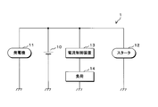
- FIG. 2 is a block diagram showing a main configuration of the power supply device 1 according to the present embodiment.
- the power supply device 1 is suitably mounted on a vehicle and includes a battery 10, a generator 11, a starter 12, a current control device 13, and a load 14.
- the positive electrode of the battery 10 is connected to one end of each of the generator 11, the starter 12 and the current control device 13.
- the other end of the current control device 13 is connected to one end of the load 14.
- the negative electrode of the battery 10 and the other end of each of the generator 11, the starter 12, and the load 14 are grounded.
- the generator 11 generates electric power in conjunction with an engine (not shown) and supplies the generated electric power to the battery 10. Thereby, the battery 10 is charged.
- the battery 10 supplies power to the starter 12 and also supplies power to the load 14 via the current control device 13.
- the starter 12 is used to start the engine.
- the starter 12 operates using the power of the battery 10.
- the starter 12 operates in a state where the engine is stopped, in other words, in a state where the generator 11 stops generating power.
- the starter 12 is supplied with a large current from the battery 10 while operating.
- An internal resistor (not shown) is provided in the battery 10, and a voltage is output from the battery 10 through the internal resistor.
- the load 14 is an electric device mounted on the vehicle, for example, an ECU (Electronic Control Unit), and operates not only while the engine is operating but also when the engine is stopped.
- the load 14 is supplied with power from the battery 10 via the current control device 13.
- the current control device 13 controls the current in the current path from the battery 10 to the load 14.
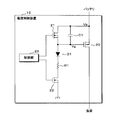
- FIG. 3 is a circuit diagram of the current control device 13.
- the current control device 13 includes a P-channel type FET 20, N-channel type FETs 21 and 22, a control unit 23, a capacitor C1, a diode D1, and a resistor R1.
- the source of the FET 20 is connected to the positive electrode of the battery 10, and the drain of the FET 20 is connected to one end of the load 14.
- the source of the FET 20 is further connected to the drain of the FET 21 and one end of the capacitor C1.
- the source of the FET 21 and the other end of the capacitor C1 are connected to the gate of the FET 20.
- the anode of the diode D1 is further connected to the gate of the FET 20, and the cathode of the diode D1 is connected to one end of the resistor R1.
- the other end of the resistor R1 is connected to the drain of the FET 22.
- the source of the FET 22 is grounded.
- the gates of the FETs 21 and 22 are connected to the control unit 23 separately.
- the capacitor C1 is connected between the source and gate of the FET 20.
- the FET 21 is connected between the source and gate of the FET 20, and the drain of the FET 22 is connected to the other end of the capacitor C1 and a connection node between the gates of the FET 20 via the diode D1 and the resistor R1.
- the FET 20 functions as a switch.
- the FET 20 has a source, a drain, and a gate as terminals.
- the current is input to the source of the FET 20, and is output from the drain of the FET 20 to the load 14.
- the FET 20 is turned on when the gate voltage with respect to the source potential is less than the negative reference voltage, and current can flow between the drain and the source in the FET 20.
- the FET 20 is turned off when the gate voltage relative to the source potential is equal to or higher than the reference voltage, and no current flows between the drain and the source in the FET 20.
- the FET 20 functions as a semiconductor switch.
- the gate functions as a control terminal
- the source functions as an input terminal.
- the current control device 13 controls the current flowing through the current path by turning on / off the FET 20 provided in the current path from the battery 10 to the load 14.
- FET21 and 22 each function as a switch.
- Each of the FETs 21 and 22 has a source, a drain, and a gate as terminals.
- Each of the FETs 21 and 22 is turned on when the gate voltage with respect to the source potential is equal to or higher than a certain voltage, and in each of the FETs 21 and 22, a current can flow between the drain and the source. Further, each of the FETs 21 and 22 is turned off when the gate voltage relative to the source potential is less than a certain voltage, and no current flows between the drain and the source in each of the FETs 21 and 22.
- the FET 21 functions as a first switch
- the FET 22 functions as a second switch.
- the control unit 23 has a CPU (Central Processing Unit) and executes various processes by executing a control program stored in a ROM (Read Only Memory) (not shown).
- the controller 23 turns the FETs 21 and 22 on and off separately by adjusting the gate voltages of the FETs 21 and 22.
- the control unit 23 turns on the FET 20 by turning off and on the FETs 21 and 22, and turns off the FET 20 by turning on and off the FETs 21 and 22, respectively.
- the output voltage of the battery 10 that is, the source voltage of the FET 20 with reference to the ground potential is described as Vb
- the gate voltage of the FET 20 with reference to the ground potential is described as Vg.
- the gate voltage with respect to the source potential is expressed by (Vg ⁇ Vb) and is equal to or less than zero volts.
- the control unit 23 turns the FETs 21 and 22 off and on, the current flows in the order of the capacitor C1, the diode D1, the resistor R1, and the FET 22 from the positive electrode of the battery 10, and the capacitor C1 is charged.
- the power stored in the capacitor C1 increases, the voltage across the capacitor C1 increases, and the gate voltage (Vg ⁇ Vb) of the FET 20 with respect to the source potential of the FET 20 decreases. Due to the storage of the capacitor C1, the voltage (Vg ⁇ Vb) becomes less than the reference voltage, and the FET 20 is turned on. As a result, the battery 10 supplies power to the load 14 via the FET 20.
- the current control device 13 has a current path that flows from the source of the FET 20 in the order of the capacitor C1, the diode D1, the resistor R1, and the FET 22. This current path functions as a second current path.
- An FET 22 is provided in a current path that flows from the source of the FET 20 through the capacitor C1.
- control unit 23 When the control unit 23 turns each of the FETs 21 and 22 on and off, the output voltage Vb and the voltage Vg match or substantially coincide with each other. It becomes. Thereby, the FET 20 is turned off, and the power supply from the battery 10 to the load 14 is stopped.
- control unit 23 Since the control unit 23 turns on the FET 21 and turns off the FET 22, no current flows from the positive electrode of the battery 10 through the FET 22 while the FET 20 is turned off. For this reason, while the control unit 23 turns off the FET 20, no power is consumed by the resistor R1, and the power consumption of the current control device 13 is small.
- the load 14 operates not only during the operation of the engine but also during the operation of the engine, and the FET 20 is kept on by the control unit 23 while the load 14 is operating. Then, as described above, the output voltage Vb of the battery 10 decreases when the starter 12 operates. In the current control device 13, the FET 20 can be kept on even when the output voltage Vb of the battery 10 decreases.
- FIG. 4 is a timing chart for explaining the effect of the current control device 13.
- the transition of the output voltage Vb is indicated by a thick line
- the transition of the voltage Vg is indicated by a thin line.
- the control unit 23 turns off and on the FETs 21 and 22 in order to turn on the FET 20.
- the control unit 23 turns the FETs 21 and 22 off and on, so the voltage (Vg ⁇ Vb) is less than the reference voltage and the FET 20 is on. At this time, the voltage Vg substantially matches the forward voltage difference of the diode D1, for example, 0.7 volts, and is equal to or greater than zero volts.
- the starter 12 When the starter 12 is activated and the output voltage Vb of the battery 10 is lowered, the voltage Vg is also lowered by the capacitor C1. For this reason, since the voltage (Vb ⁇ Vg) after the starter 12 is operated is the same as or substantially the same as the voltage (Vb ⁇ Vg) before the starter 12 is operated, the output voltage Vb of the battery 10 is reduced in the FET 20. It stays on while you're on.
- the diode D1 prevents the backflow of current in the current path through which current flows from the source of the FET 20 via the capacitor C1. For this reason, even when the voltage Vg is reduced to a voltage lower than zero volts due to the decrease in the output voltage Vb of the battery 10, the current flows in the order of the FET 22, the resistor R1, the diode D1, and the capacitor C1, that is, the current flows. There is no backflow. Thus, the diode D1 functions as a backflow prevention element.
- the output voltage Vb of the battery 10 returns to the voltage before the starter 12 is activated.
- the voltage Vg increases as the output voltage Vb of the battery 10 increases. For this reason, after the starter 12 stops, the voltage Vg also returns to the voltage before the starter 12 is activated, like the output voltage Vb of the battery 10.
- the configuration for turning on / off the FET 20 is not limited to the configuration for turning on / off the FET 20 by turning on / off the FETs 21 and 22.
- the FET 22 may not be provided, and the other end of the resistor R1 may be grounded.
- the control unit 23 turns on the FET 20 by turning off the FET 21, and turns off the FET 20 by turning on the FET 21.
- each of the FETs 21 and 22 may function as a switch. For this reason, each of the FETs 21 and 22 is not limited to an N-channel FET, and may be a P-channel FET. Further, bipolar transistors may be used instead of the FETs 21 and 22.
- the voltage Vg is lowered. , FET 20 remains on.
Landscapes
- Electronic Switches (AREA)
- Charge And Discharge Circuits For Batteries Or The Like (AREA)
Abstract
電流が入力される半導体スイッチの端子の電位が低下した場合であっても、半導体スイッチのオンを維持することができる電流制御装置を提供する。 電流制御装置13では、バッテリから負荷への電流経路に設けられたFET20をオン/オフすることによって該電流経路に流れる電流を制御する。FET20において、電流は、ソースに入力され、ドレインから出力される。FET20は、ソースの電位を基準としたゲートの電圧が負の基準電圧未満である場合にオンになる。FET20のソース及びゲート間にはコンデンサC1が設けられている。ダイオードD1は、FET20のソースからコンデンサC1を介して電流が流れる電流経路における電流の逆流を防止する。
Description
本発明は、電流経路に設けられたスイッチをオン/オフすることによって該電流経路に流れる電流を制御する電流制御装置に関する。
現在、車両には、バッテリからスイッチを介して負荷に給電される電源装置(例えば特許文献1)が搭載されている。
図1は従来の電源装置8の回路図である。従来の電源装置8では、バッテリ80の正極がPチャネル型のFET(Field Effect Transistor)81のソースに接続されており、FET81のドレインは負荷82の一端に接続されている。バッテリ80の負極と負荷82の他端とは接地されている。
FET81はスイッチとして機能する。FET81は、ソースの電位を基準としたゲートの電圧が負の所定電圧未満である場合にオンとなり、FET81のソース及びドレイン間に電流が流れることが可能となる。電流は、バッテリ80の正極からFET81のソースに入力し、FET81のドレインから出力される。FET81は、ソース電位を基準としたゲートの電圧が所定電圧以上である場合にオフとなり、FET81のソース及びドレイン間に電流が流れることはない。
従来の電源装置8では、ゲートの電位を接地電位に調整することによって、FET81をオンにし、ゲートの電位をソースの電位と略同じ電位に調整することによってFET81をオフにする。このように、FET81をオン/オフすることによって、バッテリ80から負荷82への電流経路に流れる電流を制御している。
しかしながら、バッテリ80の出力電圧は変動する。例えば、バッテリ80が、負荷82の他に、エンジンを始動するためのスタータに給電するように構成してある場合、スタータが作動している間、バッテリ80はスタータに大きな電流を供給する。また、バッテリ80では図示しない内部抵抗を介して電圧が出力される。このため、大きな電流がバッテリ80から出力された場合、バッテリ80の内部抵抗において電圧が大きく降下し、バッテリ80の出力電圧が低下する。
FET81がオンであり、かつ、負荷82が作動している場合において、バッテリ80の出力電圧が低下したとき、ソースの電位が低下してゲートの電位である接地電位に近づくので、ソースの電位を基準としたFET81のゲートの電圧が上昇して所定電圧以上となる虞がある。ソースの電位を基準としたゲートの電圧が所定電圧以上となった場合、FET81はオフとなり、負荷82が不意に動作を停止する。
本発明は斯かる事情に鑑みてなされたものであり、その目的とするところは、電流が入力される半導体スイッチの端子の電位が低下した場合であっても、半導体スイッチのオンを維持することができる電流制御装置を提供することにある。
本発明に係る電流制御装置は、電流経路に設けられた半導体スイッチをオン/オフすることによって該電流経路を流れる電流を制御する電流制御装置において、前記半導体スイッチは、電流が入力される入力端子の電位を基準とした制御端子の電圧が負の所定電圧未満である場合にオンとなるように構成してあり、前記入力端子及び制御端子間に接続されるコンデンサと、前記入力端子から該コンデンサを介して電流が流れる第2の電流経路と、該第2の電流経路における電流の逆流を防止する逆流防止素子とを備えることを特徴とする。
本発明にあっては、例えば、バッテリから負荷への電流経路に半導体スイッチが設けられており、半導体スイッチをオン/オフすることによって電流経路を流れる電流を制御する。半導体スイッチにおいて、電流が入力される入力端子の電位を基準とした制御端子の電圧が負の所定電圧未満である場合、半導体スイッチはオンとなる。半導体スイッチは例えばPチャネル型のFETである。
半導体スイッチの入力端子及び制御端子間にコンデンサが接続されており、第2の電流経路では入力端子からコンデンサを介して電流が流れる。第2の電流経路に電流が流れることによって、コンデンサに電力が蓄えられる。蓄電によってコンデンサの両端間の電圧が上昇し、入力端子の電位を基準とした制御端子の電圧が所定電圧未満となり、半導体スイッチがオンとなる。
半導体スイッチがオンである状態で入力端子の電位が低下した場合、コンデンサによって、制御端子の電位も低下する。このため、入力端子の電位が低下した場合であっても、入力端子の電位を基準とした制御端子の電圧は変わらないため、半導体スイッチのオンが維持される。また、逆流防止素子、例えばダイオードによって第2の電流経路における電流の逆流が防止されるため、第2の電流経路においては、制御端子の電位の低下によって電流が逆流することはない。
本発明に係る電流制御装置は、前記入力端子及び制御端子間に接続してある第1スイッチと、前記第2の電流経路に設けられており、一端が前記コンデンサ及び第1スイッチ間の接続ノードに接続してある第2スイッチとを備え、前記半導体スイッチは、前記制御端子の電圧が前記所定電圧以上である場合にオフとなり、前記第1スイッチ及び第2スイッチ夫々をオン及びオフにすることによって前記半導体スイッチをオフにするように構成してあることを特徴とする。
本発明にあっては、半導体スイッチの入力端子及び制御端子間に第1スイッチが接続してあり、第2の電流経路に第2スイッチが設けられている。第2スイッチの一端はコンデンサ及び第1スイッチ間の接続ノードに接続してある。半導体スイッチは、入力端子の電位を基準とした制御端子の電圧が負の所定電圧以上である場合にオフとなる。第1スイッチをオンにすることによって、半導体スイッチの入力端子及び制御端子間の電圧はゼロボルトとなり、半導体スイッチはオフとなる。
このとき、第2スイッチはオフとなっているので、第2スイッチを介して電流が流れることはなく、消費電力が小さい。
このとき、第2スイッチはオフとなっているので、第2スイッチを介して電流が流れることはなく、消費電力が小さい。
本発明によれば、電流が入力される半導体スイッチの端子の電位が低下した場合であっても、半導体スイッチのオンを維持することができる。
以下、本発明をその実施の形態を示す図面に基づいて詳述する。
図2は、本実施の形態における電源装置1の要部構成を示すブロック図である。電源装置1は車両に好適に搭載されており、バッテリ10、発電機11、スタータ12、電流制御装置13及び負荷14を備える。バッテリ10の正極は、発電機11、スタータ12及び電流制御装置13夫々の一端に接続されている。電流制御装置13の他端は負荷14の一端に接続されている。バッテリ10の負極と、発電機11、スタータ12及び負荷14夫々の他端とは接地されている。
図2は、本実施の形態における電源装置1の要部構成を示すブロック図である。電源装置1は車両に好適に搭載されており、バッテリ10、発電機11、スタータ12、電流制御装置13及び負荷14を備える。バッテリ10の正極は、発電機11、スタータ12及び電流制御装置13夫々の一端に接続されている。電流制御装置13の他端は負荷14の一端に接続されている。バッテリ10の負極と、発電機11、スタータ12及び負荷14夫々の他端とは接地されている。
発電機11は、図示しないエンジンに連動して電力を発生し、発生した電力をバッテリ10に供給する。これにより、バッテリ10は充電される。バッテリ10は、スタータ12に給電すると共に、電流制御装置13を介して負荷14に給電する。
スタータ12はエンジンを始動させるために用いられる。スタータ12はバッテリ10の電力を用いて作動する。当然のことながら、スタータ12は、エンジンが停止している状態、言い換えると、発電機11が発電を停止している状態で作動する。スタータ12は、作動している間、バッテリ10から大きな電流が供給される。バッテリ10内には図示しない内部抵抗が設けられており、内部抵抗を介して電圧がバッテリ10から出力される。バッテリ10からスタータ12に大きな電力が供給された場合、内部抵抗において電圧が大きく降下し、バッテリ10の出力電圧が低下する。
負荷14は、車両に搭載される電気機器、例えばECU(Electronic Control Unit)であり、エンジンの作動中だけではなく、エンジンの停止中も作動する。負荷14は、電流制御装置13を介して、バッテリ10から給電される。
電流制御装置13は、バッテリ10から負荷14への電流経路の電流を制御する。
電流制御装置13は、バッテリ10から負荷14への電流経路の電流を制御する。
図3は電流制御装置13の回路図である。電流制御装置13は、Pチャネル型のFET20、Nチャネル型のFET21,22、制御部23、コンデンサC1、ダイオードD1及び抵抗R1を有する。FET20のソースはバッテリ10の正極に接続されており、FET20のドレインは負荷14の一端に接続されている。FET20のソースには、更に、FET21のドレインと、コンデンサC1の一端とが接続されている。FET21のソースと、コンデンサC1の他端とはFET20のゲートに接続されている。
FET20のゲートには、ダイオードD1のアノードが、更に接続されており、ダイオードD1のカソードは抵抗R1の一端に接続されている。抵抗R1の他端はFET22のドレインに接続されている。FET22のソースは接地されている。FET21,22夫々のゲートは制御部23に各別に接続されている。
以上のように、コンデンサC1は、FET20のソース及びゲート間に接続される。FET21は、FET20のソース及びゲート間に接続してあり、FET22のドレインは、ダイオードD1及び抵抗R1を介して、コンデンサC1の他端、及び、FET20のゲート間の接続ノードに接続してある。
FET20はスイッチとして機能する。FET20は、端子として、ソース、ドレイン及びゲートを有する。FET20において、電流はFET20のソースに入力し、FET20のドレインから負荷14に出力される。FET20は、ソースの電位を基準としたゲートの電圧が負の基準電圧未満である場合にオンとなり、FET20において電流がドレイン及びソース間を流れることが可能となる。FET20は、ソースの電位を基準としたゲートの電圧が基準電圧以上である場合にオフとなり、FET20において電流がドレイン及びソース間を流れることはない。FET20は半導体スイッチとして機能する。FET20において、ゲートは制御端子として機能し、ソースは入力端子として機能する。
電流制御装置13では、バッテリ10から負荷14への電流経路に設けられたFET20をオン/オフすることによって、該電流経路に流れる電流を制御する。
FET21,22夫々もスイッチとして機能する。FET21,22夫々も、端子として、ソース、ドレイン及びゲートを有する。FET21,22夫々は、ソースの電位を基準としたゲートの電圧が一定電圧以上である場合にオンとなり、FET21,22夫々において、電流がドレイン及びソース間を流れることが可能となる。また、FET21,22夫々は、ソースの電位を基準としたゲートの電圧が一定電圧未満である場合にオフとなり、FET21,22夫々において、電流がドレイン及びソース間を流れることはない。FET21は第1スイッチとして機能し、FET22は第2スイッチとして機能する。
制御部23は、CPU(Central Processing Unit)を有し、図示しないROM(Read Only Memory)に記憶してある制御プログラムを実行することによって種々の処理を実行する。制御部23は、FET21,22夫々のゲートの電圧を調整することによって、FET21,22を各別にオン/オフする。制御部23は、FET21,22夫々をオフ及びオンにすることによってFET20をオンにし、FET21,22夫々をオン及びオフにすることによってFET20をオフにする。
以下では、バッテリ10の出力電圧、即ち、接地電位を基準としたFET20のソースの電圧をVbと記載し、接地電位を基準としたFET20のゲートの電圧をVgと記載する。FET20において、ソースの電位を基準としたゲートの電圧は、(Vg-Vb)で表され、ゼロボルト以下である。
制御部23がFET21,22夫々をオフ及びオンにした場合、電流がバッテリ10の正極からコンデンサC1、ダイオードD1、抵抗R1及びFET22の順に流れ、コンデンサC1が蓄電される。コンデンサC1が蓄えている電力が増加した場合、コンデンサC1の両端間の電圧が上昇し、FET20のソースの電位を基準としたFET20のゲートの電圧(Vg-Vb)は低下する。コンデンサC1の蓄電によって、電圧(Vg-Vb)は基準電圧未満となり、FET20はオンとなる。これにより、バッテリ10はFET20を介して負荷14に給電する。
以上のように、電流制御装置13は、FET20のソースから、コンデンサC1、ダイオードD1、抵抗R1及びFET22の順に流れる電流経路を有する。この電流経路は第2の電流経路として機能する。FET20のソースからコンデンサC1を介して流れる電流経路にはFET22が設けられている。
制御部23がFET21,22夫々をオン及びオフにした場合、出力電圧Vbと電圧Vgとが一致又は略一致するため、FET20において、電圧(Vg-Vb)はゼロボルト又は略ゼロボルトとなり、基準電圧以上となる。これにより、FET20はオフとなり、バッテリ10から負荷14への給電が停止する。
制御部23は、FET21をオンにすると共にFET22をオフするため、FET20をオフにしている間、バッテリ10の正極からFET22を介して電流が流れることはない。このため、制御部23がFET20をオフにしている間、抵抗R1で電力が消費されることはなく、電流制御装置13の消費電力は小さい。
前述したように、負荷14はエンジンの作動中だけではなくエンジンの動作中も作動し、負荷14が作動している間、制御部23によってFET20はオンに維持されている。そして、バッテリ10の出力電圧Vbは、前述したように、スタータ12が作動した場合、低下する。電流制御装置13では、バッテリ10の出力電圧Vbが低下した場合であっても、FET20のオンを維持することができる。
図4は電流制御装置13の効果を説明するためのタイミングチャートである。図4では、出力電圧Vbの推移が太線で示されており、電圧Vgの推移が細線で示されている。以下では、制御部23は、FET20をオンにするため、FET21,22夫々をオフ及びオンにしているとする。
スタータ12が作動する前において、制御部23がFET21,22をオフ及びオンにしているため、電圧(Vg-Vb)が基準電圧未満となっており、FET20はオンである。このとき、電圧Vgは、ダイオードD1の順方向の電圧差、例えば、0.7ボルトに略一致し、ゼロボルト以上である。
スタータ12が作動してバッテリ10の出力電圧Vbが低下した場合、コンデンサC1によって、電圧Vgも低下する。このため、スタータ12の作動後における電圧(Vb-Vg)は、スタータ12の作動前における電圧(Vb-Vg)と同じ又は略同じであるため、FET20は、バッテリ10の出力電圧Vbが低下している間もオンに維持される。
ダイオードD1は、FET20のソースからコンデンサC1を介して電流が流れる電流経路における電流の逆流を防止する。このため、バッテリ10の出力電圧Vbの低下によって、電圧Vgがゼロボルト未満の電圧に低下した場合であっても、電流がFET22、抵抗R1、ダイオードD1及びコンデンサC1の順に流れること、即ち、電流が逆流することはない。このように、ダイオードD1は逆流防止素子として機能する。
エンジンが始動してスタータ12が停止した後、バッテリ10の出力電圧Vbは、スタータ12が作動する前の電圧に戻る。電圧Vgはバッテリ10の出力電圧Vbの上昇と共に上昇する。このため、スタータ12が停止した後、電圧Vgも、バッテリ10の出力電圧Vbと同様に、スタータ12が作動する前の電圧に戻る。
なお、FET20をオン/オフする構成は、FET21,22をオン/オフすることによってFET20をオン/オフする構成に限定されない。例えば、FET22はなくてもよく、抵抗R1の他端が接地されていてもよい。この場合、制御部23は、FET21をオフにすることによってFET20をオンにし、FET21をオンにすることによってFET20をオフにする。
また、FET20の代わりにPNP型のバイポーラトランジスタが用いてられてもよい。FET21,22夫々はスイッチとして機能すればよい。このため、FET21,22夫々は、Nチャネル型のFETに限定されず、Pチャネル型のFETであってもよい。更に、FET21,22の代わりにバイポーラトランジスタを用いてもよい。
当然のことながら、電流制御装置13では、FET20がオンである状態で、スタータ12の作動以外の他の原因によってバッテリ10の出力電圧Vbが低下した場合であっても、電圧Vgは低下するため、FET20はオンを維持する。
当然のことながら、電流制御装置13では、FET20がオンである状態で、スタータ12の作動以外の他の原因によってバッテリ10の出力電圧Vbが低下した場合であっても、電圧Vgは低下するため、FET20はオンを維持する。
開示された本実施の形態は、全ての点で例示であって制限的なものではないと考えられるべきである。本発明の範囲は上述の説明ではなく請求の範囲によって示され、請求の範囲と均等の意味及び範囲内での全ての変更が含まれることが意図される。
13 電流制御装置
20 FET(半導体スイッチ)
21 FET(第1スイッチ)
22 FET(第2スイッチ)
C1 コンデンサ
D1 ダイオード(逆流防止素子)
20 FET(半導体スイッチ)
21 FET(第1スイッチ)
22 FET(第2スイッチ)
C1 コンデンサ
D1 ダイオード(逆流防止素子)
Claims (2)
- 電流経路に設けられた半導体スイッチをオン/オフすることによって該電流経路を流れる電流を制御する電流制御装置において、
前記半導体スイッチは、電流が入力される入力端子の電位を基準とした制御端子の電圧が負の所定電圧未満である場合にオンとなるように構成してあり、
前記入力端子及び制御端子間に接続されるコンデンサと、
前記入力端子から該コンデンサを介して電流が流れる第2の電流経路と、
該第2の電流経路における電流の逆流を防止する逆流防止素子と
を備えることを特徴とする電流制御装置。 - 前記入力端子及び制御端子間に接続してある第1スイッチと、
前記第2の電流経路に設けられており、一端が前記コンデンサ及び第1スイッチ間の接続ノードに接続してある第2スイッチと
を備え、
前記半導体スイッチは、前記制御端子の電圧が前記所定電圧以上である場合にオフとなり、
前記第1スイッチ及び第2スイッチ夫々をオン及びオフにすることによって前記半導体スイッチをオフにするように構成してあること
を特徴とする請求項1に記載の電流制御装置。
Applications Claiming Priority (2)
| Application Number | Priority Date | Filing Date | Title |
|---|---|---|---|
| JP2015001718A JP2016127541A (ja) | 2015-01-07 | 2015-01-07 | 電流制御装置 |
| JP2015-001718 | 2015-01-07 |
Publications (1)
| Publication Number | Publication Date |
|---|---|
| WO2016111161A1 true WO2016111161A1 (ja) | 2016-07-14 |
Family
ID=56355861
Family Applications (1)
| Application Number | Title | Priority Date | Filing Date |
|---|---|---|---|
| PCT/JP2015/085771 Ceased WO2016111161A1 (ja) | 2015-01-07 | 2015-12-22 | 電流制御装置 |
Country Status (2)
| Country | Link |
|---|---|
| JP (1) | JP2016127541A (ja) |
| WO (1) | WO2016111161A1 (ja) |
Citations (3)
| Publication number | Priority date | Publication date | Assignee | Title |
|---|---|---|---|---|
| JPS5215168Y2 (ja) * | 1973-10-22 | 1977-04-05 | ||
| JP2009044304A (ja) * | 2007-08-07 | 2009-02-26 | Denso Corp | 半導体素子制御装置 |
| JP2012157146A (ja) * | 2011-01-26 | 2012-08-16 | Nec Commun Syst Ltd | 電源装置 |
-
2015
- 2015-01-07 JP JP2015001718A patent/JP2016127541A/ja active Pending
- 2015-12-22 WO PCT/JP2015/085771 patent/WO2016111161A1/ja not_active Ceased
Patent Citations (3)
| Publication number | Priority date | Publication date | Assignee | Title |
|---|---|---|---|---|
| JPS5215168Y2 (ja) * | 1973-10-22 | 1977-04-05 | ||
| JP2009044304A (ja) * | 2007-08-07 | 2009-02-26 | Denso Corp | 半導体素子制御装置 |
| JP2012157146A (ja) * | 2011-01-26 | 2012-08-16 | Nec Commun Syst Ltd | 電源装置 |
Also Published As
| Publication number | Publication date |
|---|---|
| JP2016127541A (ja) | 2016-07-11 |
Similar Documents
| Publication | Publication Date | Title |
|---|---|---|
| US8619444B2 (en) | Voltage booster system and semiconductor chip | |
| JP6531695B2 (ja) | 電源システム | |
| JP6492507B2 (ja) | 電子制御装置 | |
| US20130113446A1 (en) | Power supply with integrated voltage clamp and current sink | |
| JP2016045873A (ja) | 電源電圧検知回路 | |
| JP2994572B2 (ja) | ヒステリシス比較器を備えた電圧制限回路 | |
| CN104518666A (zh) | 感应性负载的供电控制装置 | |
| JP2017135532A (ja) | 電圧検出回路及びチャージポンプ回路 | |
| KR20160070004A (ko) | 전압 검출 회로 | |
| WO2017122664A1 (ja) | 給電制御装置 | |
| JP5123679B2 (ja) | 基準電圧生成回路及びその起動制御方法 | |
| JP2013241080A (ja) | 車両用電源制御回路 | |
| JP5637096B2 (ja) | バンドギャップ基準電圧回路及びこれを用いたパワーオンリセット回路 | |
| JP2008193283A (ja) | 整流装置 | |
| US10084311B2 (en) | Voltage generator | |
| US20210281105A1 (en) | Circuit device | |
| JP2013255002A (ja) | 低電圧ロックアウト回路 | |
| US20130002019A1 (en) | Circuit, Method for Operating a Circuit, and Use | |
| JP2011077698A (ja) | 負荷駆動装置 | |
| WO2021033630A1 (ja) | スイッチ装置 | |
| JP2016127541A (ja) | 電流制御装置 | |
| JP2013247823A (ja) | 半導体装置 | |
| WO2018147102A1 (ja) | スイッチ制御装置 | |
| JP3996147B2 (ja) | わずかな充電電流を用いたブートストラップキャパシタ充電回路 | |
| WO2018066499A1 (ja) | 車載機器 |
Legal Events
| Date | Code | Title | Description |
|---|---|---|---|
| 121 | Ep: the epo has been informed by wipo that ep was designated in this application |
Ref document number: 15877034 Country of ref document: EP Kind code of ref document: A1 |
|
| NENP | Non-entry into the national phase |
Ref country code: DE |
|
| 122 | Ep: pct application non-entry in european phase |
Ref document number: 15877034 Country of ref document: EP Kind code of ref document: A1 |