WO2016104684A1 - ダイヤモンド半導体デバイス - Google Patents
ダイヤモンド半導体デバイス Download PDFInfo
- Publication number
- WO2016104684A1 WO2016104684A1 PCT/JP2015/086187 JP2015086187W WO2016104684A1 WO 2016104684 A1 WO2016104684 A1 WO 2016104684A1 JP 2015086187 W JP2015086187 W JP 2015086187W WO 2016104684 A1 WO2016104684 A1 WO 2016104684A1
- Authority
- WO
- WIPO (PCT)
- Prior art keywords
- diamond
- boron
- ratio
- semiconductor device
- region
- Prior art date
- Legal status (The legal status is an assumption and is not a legal conclusion. Google has not performed a legal analysis and makes no representation as to the accuracy of the status listed.)
- Ceased
Links
Images


Classifications
-
- H—ELECTRICITY
- H10—SEMICONDUCTOR DEVICES; ELECTRIC SOLID-STATE DEVICES NOT OTHERWISE PROVIDED FOR
- H10D—INORGANIC ELECTRIC SEMICONDUCTOR DEVICES
- H10D8/00—Diodes
- H10D8/60—Schottky-barrier diodes
-
- C—CHEMISTRY; METALLURGY
- C01—INORGANIC CHEMISTRY
- C01B—NON-METALLIC ELEMENTS; COMPOUNDS THEREOF; METALLOIDS OR COMPOUNDS THEREOF NOT COVERED BY SUBCLASS C01C
- C01B32/00—Carbon; Compounds thereof
- C01B32/25—Diamond
- C01B32/26—Preparation
-
- H—ELECTRICITY
- H10—SEMICONDUCTOR DEVICES; ELECTRIC SOLID-STATE DEVICES NOT OTHERWISE PROVIDED FOR
- H10D—INORGANIC ELECTRIC SEMICONDUCTOR DEVICES
- H10D30/00—Field-effect transistors [FET]
- H10D30/80—FETs having rectifying junction gate electrodes
- H10D30/87—FETs having Schottky gate electrodes, e.g. metal-semiconductor FETs [MESFET]
-
- H—ELECTRICITY
- H10—SEMICONDUCTOR DEVICES; ELECTRIC SOLID-STATE DEVICES NOT OTHERWISE PROVIDED FOR
- H10D—INORGANIC ELECTRIC SEMICONDUCTOR DEVICES
- H10D62/00—Semiconductor bodies, or regions thereof, of devices having potential barriers
- H10D62/80—Semiconductor bodies, or regions thereof, of devices having potential barriers characterised by the materials
- H10D62/83—Semiconductor bodies, or regions thereof, of devices having potential barriers characterised by the materials being Group IV materials, e.g. B-doped Si or undoped Ge
- H10D62/8303—Diamond
-
- H—ELECTRICITY
- H10—SEMICONDUCTOR DEVICES; ELECTRIC SOLID-STATE DEVICES NOT OTHERWISE PROVIDED FOR
- H10D—INORGANIC ELECTRIC SEMICONDUCTOR DEVICES
- H10D62/00—Semiconductor bodies, or regions thereof, of devices having potential barriers
- H10D62/80—Semiconductor bodies, or regions thereof, of devices having potential barriers characterised by the materials
- H10D62/83—Semiconductor bodies, or regions thereof, of devices having potential barriers characterised by the materials being Group IV materials, e.g. B-doped Si or undoped Ge
- H10D62/834—Semiconductor bodies, or regions thereof, of devices having potential barriers characterised by the materials being Group IV materials, e.g. B-doped Si or undoped Ge further characterised by the dopants
-
- H—ELECTRICITY
- H10—SEMICONDUCTOR DEVICES; ELECTRIC SOLID-STATE DEVICES NOT OTHERWISE PROVIDED FOR
- H10P—GENERIC PROCESSES OR APPARATUS FOR THE MANUFACTURE OR TREATMENT OF DEVICES COVERED BY CLASS H10
- H10P14/00—Formation of materials, e.g. in the shape of layers or pillars
- H10P14/20—Formation of materials, e.g. in the shape of layers or pillars of semiconductor materials
- H10P14/24—Formation of materials, e.g. in the shape of layers or pillars of semiconductor materials using chemical vapour deposition [CVD]
-
- H—ELECTRICITY
- H10—SEMICONDUCTOR DEVICES; ELECTRIC SOLID-STATE DEVICES NOT OTHERWISE PROVIDED FOR
- H10P—GENERIC PROCESSES OR APPARATUS FOR THE MANUFACTURE OR TREATMENT OF DEVICES COVERED BY CLASS H10
- H10P14/00—Formation of materials, e.g. in the shape of layers or pillars
- H10P14/20—Formation of materials, e.g. in the shape of layers or pillars of semiconductor materials
- H10P14/29—Formation of materials, e.g. in the shape of layers or pillars of semiconductor materials characterised by the substrates
- H10P14/2901—Materials
- H10P14/2902—Materials being Group IVA materials
- H10P14/2903—Carbon, e.g. diamond-like carbon
-
- H—ELECTRICITY
- H10—SEMICONDUCTOR DEVICES; ELECTRIC SOLID-STATE DEVICES NOT OTHERWISE PROVIDED FOR
- H10P—GENERIC PROCESSES OR APPARATUS FOR THE MANUFACTURE OR TREATMENT OF DEVICES COVERED BY CLASS H10
- H10P14/00—Formation of materials, e.g. in the shape of layers or pillars
- H10P14/20—Formation of materials, e.g. in the shape of layers or pillars of semiconductor materials
- H10P14/29—Formation of materials, e.g. in the shape of layers or pillars of semiconductor materials characterised by the substrates
- H10P14/2926—Crystal orientations
-
- H—ELECTRICITY
- H10—SEMICONDUCTOR DEVICES; ELECTRIC SOLID-STATE DEVICES NOT OTHERWISE PROVIDED FOR
- H10P—GENERIC PROCESSES OR APPARATUS FOR THE MANUFACTURE OR TREATMENT OF DEVICES COVERED BY CLASS H10
- H10P14/00—Formation of materials, e.g. in the shape of layers or pillars
- H10P14/20—Formation of materials, e.g. in the shape of layers or pillars of semiconductor materials
- H10P14/34—Deposited materials, e.g. layers
- H10P14/3402—Deposited materials, e.g. layers characterised by the chemical composition
- H10P14/3404—Deposited materials, e.g. layers characterised by the chemical composition being Group IVA materials
- H10P14/3406—Carbon, e.g. diamond-like carbon
-
- H—ELECTRICITY
- H10—SEMICONDUCTOR DEVICES; ELECTRIC SOLID-STATE DEVICES NOT OTHERWISE PROVIDED FOR
- H10P—GENERIC PROCESSES OR APPARATUS FOR THE MANUFACTURE OR TREATMENT OF DEVICES COVERED BY CLASS H10
- H10P14/00—Formation of materials, e.g. in the shape of layers or pillars
- H10P14/20—Formation of materials, e.g. in the shape of layers or pillars of semiconductor materials
- H10P14/34—Deposited materials, e.g. layers
- H10P14/3438—Doping during depositing
- H10P14/3441—Conductivity type
- H10P14/3444—P-type
-
- H—ELECTRICITY
- H10—SEMICONDUCTOR DEVICES; ELECTRIC SOLID-STATE DEVICES NOT OTHERWISE PROVIDED FOR
- H10P—GENERIC PROCESSES OR APPARATUS FOR THE MANUFACTURE OR TREATMENT OF DEVICES COVERED BY CLASS H10
- H10P30/00—Ion implantation into wafers, substrates or parts of devices
- H10P30/20—Ion implantation into wafers, substrates or parts of devices into semiconductor materials, e.g. for doping
-
- H—ELECTRICITY
- H10—SEMICONDUCTOR DEVICES; ELECTRIC SOLID-STATE DEVICES NOT OTHERWISE PROVIDED FOR
- H10D—INORGANIC ELECTRIC SEMICONDUCTOR DEVICES
- H10D64/00—Electrodes of devices having potential barriers
- H10D64/60—Electrodes characterised by their materials
- H10D64/62—Electrodes ohmically coupled to a semiconductor
-
- H—ELECTRICITY
- H10—SEMICONDUCTOR DEVICES; ELECTRIC SOLID-STATE DEVICES NOT OTHERWISE PROVIDED FOR
- H10D—INORGANIC ELECTRIC SEMICONDUCTOR DEVICES
- H10D64/00—Electrodes of devices having potential barriers
- H10D64/60—Electrodes characterised by their materials
- H10D64/64—Electrodes comprising a Schottky barrier to a semiconductor
Definitions
- the present invention relates to a diamond semiconductor device, and more particularly to a diamond semiconductor device having high resistance to radiation.
- Diamond is a wide band gap semiconductor with a wide forbidden band of about 5.5 eV, and has the advantage of being able to operate under high radiation resistance and a high temperature environment of about 800 ° C. Therefore, it is expected as a material for semiconductor devices used in high temperature and high radiation environments such as sensors and preamplifiers used in nuclear reactors, fusion reactors, accelerators and the like.
- diamond Compared to Si, which is a common material for semiconductor devices, diamond has a resistance of four orders of magnitude or more against high energy photons such as ⁇ rays and X rays.
- high energy photons such as ⁇ rays and X rays.
- thermal neutrons represented by thermal neutrons
- the reaction of the following formula (1) occurs in Si, and phosphorus (P) acting as an n-type dopant is generated with respect to Si, resulting in semiconductor characteristics. Although it deteriorates, such a nuclear reaction does not occur in diamond whose constituent element is C, and there is no deterioration in semiconductor characteristics.
- the nuclear reaction of the above formula (1) is used as a semiconductor doping technique.
- it is used as a method of converting 10 B doped into diamond into Li to form an n-type dopant (for example, Patent Document 1). reference).
- Diamond does not deteriorate the semiconductor characteristics due to the nuclear reaction of the constituent element C even when irradiated with neutrons.
- boron (B) when boron (B) is used as a p-type dopant, boron 10 B having high neutron absorption ability is used. Absorbs neutron (n) and causes a charged particle generation reaction shown in the following formula (2), and the generated charged particles Li and He affect the semiconductor characteristics.
- an object of the present invention is to provide a diamond semiconductor device that is not affected by charged particle generation reaction even when boron (B) is used as a p-type dopant.
- the present invention has a p-type region made of diamond, and the p-type impurity of the p-type region is made of boron containing two isotopes of 10 B and 11 B, and the concentration ratio of isotopes contained in the p-type region ( 10 B / 11 B) is a diamond semiconductor device characterized by being smaller than the natural abundance ratio of isotopes.
- the diamond semiconductor device according to the present invention has high resistance to radiation, particularly neutrons, and can be used without causing deterioration of characteristics even in the presence of high ⁇ rays or neutrons.
- Boron (B) which can exist stably in nature, has two isotopes of 10 B that emits high energy charged particles and 11 B that does not emit as a result of absorbing neutrons, of which about 20% are neutrons. It is 10 B with high absorbability. For this reason, not only the diamond semiconductor device but also the Si or SiC semiconductor device uses boron as the p-type dopant, so that the reaction of the above-described formula (2) occurs and the same problem may occur.
- the ratio of 10 B having a high neutron absorption capacity is reduced to increase 11 B, that is, the p-type region.
- the boron isotope concentration ratio ( 10 B / 11 B) contained in the isotopes is made smaller than the natural abundance ratio of the isotopes, thereby suppressing the occurrence of the above formula (2) and preventing the deterioration of electrical characteristics.
- the p-type region is used as an operation layer or a p-type conductive layer, it is necessary to avoid the introduction of defects and grow so as to be flat, highly pure, and have high crystallinity.
- the ratio of the concentration of boron isotopes contained in the p-type region ( 10 B / 11 B) is made smaller than the natural abundance ratio of isotopes, and the crystallinity is further enhanced for growth.
- a diamond off-substrate with a controlled off angle is used as the substrate, and a p-type diamond layer is epitaxially grown thereon.
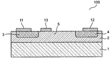
- FIG. 1 is a cross-sectional view of a field-effect transistor according to a first embodiment of the present invention, the whole being represented by 100.
- the field effect transistor 100 includes a diamond substrate 1.
- the diamond substrate 1 is made of, for example, a high pressure high temperature synthesis (HP / HT) Ib type single crystal diamond substrate, a high pressure high temperature synthesis IIa type single crystal diamond substrate, or a chemical vapor synthesis single crystal diamond substrate, and has a surface of (001).
- a surface or (111) plane substrate or an off-substrate whose surface is inclined by 0.3 to 6 ° in the ⁇ 110> direction from the (001) plane is used.
- An epitaxial layer 2 made of p-type single crystal diamond is provided on the diamond substrate 1.
- Epitaxial layer 2 contains boron as a p-type dopant. The concentration of boron is 10 14 to 10 18 atoms / cm 3 .
- a p-type (conductive layer) source region 3 and drain region 4 are provided in the epitaxial layer 2.
- the source region 3 and the drain region 4 contain boron as a p-type dopant, and the concentration of boron is 10 19 to 10 22 atoms / cm 3 .
- the epitaxial layer 2 sandwiched between the source region 3 and the drain region 4 becomes a channel region 5.
- a source electrode 11 connected to the source region 3 and a drain electrode 12 connected to the drain region 4 are provided on the epitaxial layer 2.
- a gate electrode 13 is provided on the channel region 5 so as to be sandwiched between the source electrode 11 and the drain electrode 12.
- a substrate such as a high pressure high temperature synthesis (HP / HT) Ib type single crystal diamond substrate, a high pressure high temperature synthesis IIa type single crystal diamond substrate, or a chemical vapor synthesis single crystal diamond substrate.
- a p-type diamond epitaxial layer 2 is grown thereon.
- the epitaxial layer 2 is formed using, for example, a microwave plasma chemical vapor deposition (PCVD) method, a DC arc method, or a hot filament method in a microwave plasma growth apparatus.
- the epitaxial layer 2 is grown using, for example, a hydrocarbon gas such as methane, ethane, butane or propane as a material gas, trimethylboron or diborane as a dopant gas, hydrogen as a carrier gas, and a substrate temperature of 850 ° C., for example.
- the dopant gas includes, for example, trimethylboron and diborane synthesized from boric acid enriched with boron to 11 B ⁇ 99.7%.
- the source region 3 and the drain region 4 are formed by, for example, selectively etching the epitaxial layer 2 and then selectively growing the p-type source region 3 and the drain region 4 in that portion.
- the field effect transistor 100 by reducing the proportion of 10 B having high neutron absorption ability among boron used as the p-type dopant, the occurrence of the above-described formula (2) is suppressed, and the electrical characteristics To prevent deterioration.
- Such a field effect transistor 100 is assumed to be used in a nuclear reactor application.
- a BWR reactor containment monitor (CAMS) used in a reactor containment vessel, a PWR post-accident monitor (transmitter, PAM), preamplifiers for activation system monitoring, multiplexers, etc. are conceivable.
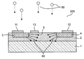
- FIG. 2 is a comparative example, and shows a cross-sectional view of a general field effect transistor, the whole being denoted by 200. 2, the same reference numerals as those in FIG. 1 indicate the same or corresponding parts.
- the field effect transistor 200 has the same structure as the field effect transistor 100 according to the first embodiment shown in FIG. 1 except for the p-type dopant contained in the source region 3, the drain region 4, and the channel region 5.
- the substrate 1 and the epitaxial layer 2 are made of diamond, and boron, which is a p-type dopant in the source region 3, the drain region 4, and the channel region 5, is 10 B and 11 B which are stable in nature.
- neutrons 50 When used in a nuclear reactor containment vessel, neutrons 50 as shown in FIG.
- the neutron 50 collides with boron in the source region 3, the drain region 4, and the channel region 5.
- the charged particle generation reaction shown in the above formula (2) occurs upon absorption.
- charged particles 60 mainly composed of 7 Li and 4 He are emitted, enter the surrounding epitaxial layer 2, damage the crystals such as the channel region 5, and deteriorate electrical characteristics such as electrical conductivity. .
- the ratio of 10 B in boron contained in the source region 3, the drain region 4, and the channel region 5 is lower than the natural abundance ratio. ) Is suppressed, and deterioration of electrical characteristics as seen in the semiconductor device 200 can be prevented.
- the evaluation example is shown below.
- Sample 1 An evaluation sample in which an epitaxial layer containing boron as a p-type dopant was formed on a diamond substrate was prepared, and the characteristics were evaluated. Specifically, a single crystal Ib type diamond substrate was prepared, and an epitaxial layer of p type diamond was grown thereon. The epitaxial layer was grown by a microwave plasma growth apparatus using a microwave plasma chemical vapor deposition (PCVD) method. The growth conditions are as follows.
- the expected film thickness of the epitaxial layer is 10.5 ⁇ m, and the p-type doping concentration is 3 to 5 ⁇ 10 17 atoms / cm 3 .
- the high-energy charged particles 7 Li and 4 He emitted from 10 B affect the electrical characteristics of diamond.
- an evaluation method it is possible to generate neutrons in a nuclear reactor or the like and directly influence the 10 B (n, 4 He) 7 Li reaction. It is also necessary to consider the effects of atomic knockout and gamma rays. Therefore, in order to evaluate only the influence caused by the charged particles, the influence on the electrical characteristics and the like was evaluated by irradiating the sample with 4 He using a charged particle accelerator. That is, 4 He generated by the reaction of the formula (2) was irradiated to the evaluation sample to evaluate the influence on the electrical characteristics and the like.
- the evaluation sample and the comparative sample were irradiated with 4 He + ions twice at 3 MeV.
- Each ion irradiation amount is as follows. 1st time: 1 ⁇ 10 12 ion / cm 2 Second time: 1 ⁇ 10 13 ion / cm 2
- evaluation was performed before the He ion irradiation, after the first irradiation, and after the second irradiation.
- the contents of evaluation were the following (1) and (2) for the comparative sample and the following (3) and (4) for the evaluation sample.
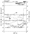
- FIG. 3 shows secondary ion mass spectrometry (SIMS) results of the evaluation samples.
- the vertical axis represents the concentration of hydrogen, boron, nitrogen, and silicon (secondary ion intensity), and the horizontal axis represents the depth from the surface of the evaluation sample.
- the surface of the diamond substrate exists at a depth of 9 ⁇ m from the surface.
- the doping concentration of 11 B is 7 ⁇ 10 14 to 4 ⁇ 10 17 atoms / cm 3
- the doping concentration of 10 B is 1 ⁇ 10 14 to 2 ⁇ 10 15 atoms / cm 3. Yes.
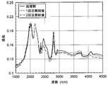
- FIG. 4 shows the FT-IR measurement results of the comparative sample before He ion irradiation, the first time, and after the second time irradiation.
- 2500cm -1 (0.305eV)
- absorption peaks relating to the electrical conductivity existing in the vicinity of 2800cm -1 (0.347eV) and 4100cm -1 (0.507eV) is before irradiation (solid line )
- the value decreases as the irradiation amount of He ions increases after the first irradiation (dashed line) and after the second irradiation (one-dot chain line). This shows that the acceptor concentration decreases as the He ion irradiation amount increases.
- FIG. 5 shows the hole measurement results of the comparative sample before He ion irradiation, after the first irradiation, and after the second irradiation, and shows changes in carrier concentration, mobility and specific resistance. As can be seen from FIG. 5, it can be seen from the values before irradiation that the carrier concentration and mobility decrease and the specific resistance increases as the irradiation amount of He ions increases after the first irradiation and after the second irradiation.
- FIG. 6 shows the results of triple-axis high-resolution rocking curve crystallinity evaluation of an evaluation sample by the X-ray diffraction (XRD) method.
- the peak position of the Raman scattered light with respect to the diamond crystal does not change before and after the He ion irradiation, and it is understood that the crystal is not distorted even when the He ion is irradiated.
- the half width of the peak wavelength hardly changes before and after the He ion irradiation, and no disorder of the crystal occurs.
- FIG. 7 is an evaluation result of level formation of an evaluation sample by ultraviolet / visible absorption (UV / VIS) measurement.
- the horizontal axis represents the wavelength of absorbed light, and the vertical axis represents the transmittance T. Evaluation was performed before He ion irradiation and after the second irradiation. As can be seen from FIG. 7, even when He ions are irradiated, the transmission characteristics of the evaluation sample hardly change, and it is understood that there are almost no defects due to He ion irradiation.
- FIG. 8 is a cross-sectional view of a MIMSFET (Metal Insulator Metal Semiconductor FET) according to the second embodiment, the whole of which is represented by 300.
- MIMSFET 300 the p + diamond epitaxial layer 20 is provided on the single crystal Ib type diamond substrate 1.
- a metal layer 21 made of, for example, Ti and an insulating layer 22 made of, for example, Al 2 O 3 are stacked.
- the source electrode 11 and the drain electrode 12 are provided on both sides of the insulating layer 22, and the gate electrode 13 is provided on the insulating layer 22.
- the p + diamond epitaxial layer 20 includes boron as a p-type dopant.
- the charged particle generation represented by the formula (2) is achieved even when irradiated with neutrons by setting the ratio of 10 B in boron contained in the p + diamond epitaxial layer 20 to be lower than the natural abundance ratio. Reaction is suppressed and deterioration of electrical characteristics can be prevented.
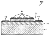
- FIG. 9 is a cross-sectional view of the Schottky diode according to the third embodiment, which is indicated as a whole by 400.
- the same reference numerals as those in FIG. 1 indicate the same or corresponding portions.
- a diamond p-type conductive layer 30 and a diamond high-purity layer 31 are laminated on a single crystal Ib type diamond substrate 1.
- an anode electrode 40 made of, for example, Au is provided on the p-type conductive layer 30 .
- a cathode electrode made of, for example, Mo or Ru is provided on the high-purity layer 31 to form a Schottky junction.
- the p-type conductive layer 30 made of diamond contains boron as a p-type dopant.
- the ratio of 10 B in boron contained in the p-type conductive layer 30 is made lower than the natural abundance ratio, so that the charged particles shown in the formula (2) even when irradiated with neutrons The production reaction is suppressed, and deterioration of electrical characteristics can be prevented.
- field effect transistors MIMSFETs, and Schottky diodes have been described.
- the present invention can be applied to diamond semiconductor devices having other p-type regions such as MISFETs, MOSFETs, bipolar transistors, etc. The radiation characteristics of can be improved.
- BWR reactor containment monitor PWR post-accident monitor (transmitter, PAM), startup system monitor It can be used as a preamplifier, multiplexer, etc.
Landscapes
- Chemical & Material Sciences (AREA)
- Organic Chemistry (AREA)
- Life Sciences & Earth Sciences (AREA)
- General Life Sciences & Earth Sciences (AREA)
- Geology (AREA)
- Inorganic Chemistry (AREA)
- Insulated Gate Type Field-Effect Transistor (AREA)
- Carbon And Carbon Compounds (AREA)
- Junction Field-Effect Transistors (AREA)
- Crystals, And After-Treatments Of Crystals (AREA)
Abstract
ダイヤモンド半導体デバイスにおいて、ダイヤモンドからなるp型領域を有し、p型領域のp型不純物は、10Bと11Bの2つの同位体を含むホウ素からなり、p型領域に含まれる同位体の濃度の比(10B/11B)は、同位体の天然存在比より小さい。
Description
本発明は、ダイヤモンド半導体デバイスに関し、特に、放射線に対して高い耐性を有するダイヤモンド半導体デバイスに関する。
ダイヤモンドは、約5.5eVの広い禁制帯幅を持つワイドバンドギャップ半導体であり、高い耐放射線特性や800℃程度の高温環境下でも動作が可能であるという長所を有する。このため原子炉、核融合炉、加速器等に使用するセンサーや前置増幅器等のような、高温、高放射線環境下で使用される半導体デバイスの材料として期待されている。
半導体デバイスの材料として一般的なSiと比較した場合、ダイヤモンドはγ線やX線のような高エネルギー光子に対して4桁以上高い耐性を有する。
また、熱中性子に代表される低エネルギー中性子を照射した場合、Siでは、以下の式(1)の反応が起こり、Siに対してn型ドーパントして働くリン(P)が生成され半導体特性が劣化するが、構成元素がCであるダイヤモンドではこのような核反応は起きず、半導体特性の劣化はない。
30Si(n,γ)31Si(T1/2=2.7h,β-)→31P......(1)
一般に、上記式(1)の核反応は、半導体のドーピング技術として用いられており、例えばダイヤモンドにドーピングした10BをLiに変換してn型ドーパントにする方法として用いられる(例えば、特許文献1参照)。
また、熱中性子に代表される低エネルギー中性子を照射した場合、Siでは、以下の式(1)の反応が起こり、Siに対してn型ドーパントして働くリン(P)が生成され半導体特性が劣化するが、構成元素がCであるダイヤモンドではこのような核反応は起きず、半導体特性の劣化はない。
30Si(n,γ)31Si(T1/2=2.7h,β-)→31P......(1)
一般に、上記式(1)の核反応は、半導体のドーピング技術として用いられており、例えばダイヤモンドにドーピングした10BをLiに変換してn型ドーパントにする方法として用いられる(例えば、特許文献1参照)。
ダイヤモンドでは、中性子が照射されても、構成元素Cの核反応に起因する半導体特性の劣化は無いが、p型ドーパントとしてホウ素(B)を用いた場合には、中性子吸収能が高いホウ素10Bが中性子(n)を吸収して以下の式(2)に示す荷電粒子生成反応を起こし、発生した荷電粒子Li、Heが半導体特性に影響を与えるという問題があった。

そこで、本発明は、p型ドーパントとしてホウ素(B)を用いても荷電粒子生成反応の影響を受けないダイヤモンド半導体デバイスの提供を目的とする。
本発明は、ダイヤモンドからなるp型領域を有し、p型領域のp型不純物は、10Bと11Bの2つの同位体を含むホウ素からなり、p型領域に含まれる同位体の濃度比(10B/11B)は、同位体の天然存在比より小さいことを特徴とするダイヤモンド半導体デバイスである。
本発明にかかるダイヤモンド半導体デバイスは、放射線、特に中性子に対する耐性が高く、例えば高γ線や中性子存在環境下でも特性の劣化を起こすことなく使用できる。
自然界で安定して存在しうるホウ素(B)には、中性子を吸収した結果、高エネルギー荷電粒子を放出する10Bと放出しない11Bの2つの同位体があるが、その約20%が中性子吸収能の高い10Bである。このため、ダイヤモンドの半導体デバイスだけでなく、SiやSiCの半導体デバイスでもp型ドーパントとしてホウ素が用いられることにより、上述の式(2)の反応が起こり、同様の問題が起こりうる。
しかしながら、SiやSiCを用いた半導体デバイスでは、中性子の照射による特性の劣化は、上述の式(1)の反応が支配的であり、式(2)に示すホウ素からの荷電粒子生成反応の影響よりも早い段階で影響が出る。このため、SiやSiCを用いた半導体デバイスでは、ホウ素からの荷電粒子生成反応の影響はこれまで殆ど問題にされてこなかった。
本発明の実施の形態では、ダイヤモンドを用いた半導体デバイスにおいて、p型ドーパントとしてホウ素を用いる場合に、中性子吸収能の高い10Bの割合を減らして11Bを増やすことにより、つまり、p型領域に含まれるホウ素の同位体の濃度の比(10B/11B)を同位体の天然存在比より小さくすることにより、上記式(2)の発生を抑制し、電気特性の劣化を防止する。
また、半導体デバイスにおいて、p型領域は動作層もしくはp型導電層として用いるため、欠陥の混入を避け、平坦かつ高純度で、高い結晶性を有するように成長する必要がある。本発明の実施の形態では、p型領域に含まれるホウ素の同位体の濃度の比(10B/11B)を同位体の天然存在比より小さくし、更に結晶性を高めて成長させるために、例えば基板としてオフ角を制御したダイヤモンドのオフ基板を用いて、その上にp型ダイヤモンド層のエピタキシャル成長を行う。
(実施の形態1)
図1は、全体が100で表される本発明の実施の形態1にかかる電界効果トランジスタの断面図である。電界効果トランジスタ100は、ダイヤモンド基板1を含む。ダイヤモンド基板1には、例えば、高圧高温合成(HP/HT)Ib型単結晶ダイヤモンド基板、高圧高温合成IIa型単結晶ダイヤモンド基板、または化学気相合成単結晶ダイヤモンド基板からなり、表面が(001)面や(111)面の基板、または表面が(001)面から<110>方向に0.3~6°傾いたオフ基板が用いられる。
図1は、全体が100で表される本発明の実施の形態1にかかる電界効果トランジスタの断面図である。電界効果トランジスタ100は、ダイヤモンド基板1を含む。ダイヤモンド基板1には、例えば、高圧高温合成(HP/HT)Ib型単結晶ダイヤモンド基板、高圧高温合成IIa型単結晶ダイヤモンド基板、または化学気相合成単結晶ダイヤモンド基板からなり、表面が(001)面や(111)面の基板、または表面が(001)面から<110>方向に0.3~6°傾いたオフ基板が用いられる。
ダイヤモンド基板1の上には、p型の単結晶ダイヤモンドからなるエピタキシャル層2を有する。エピタキシャル層2はp型ドーパントとしてホウ素を含む。ホウ素の濃度は1014~1018atom/cm3である。エピタキシャル層2の中には、p型(導電層)のソース領域3およびドレイン領域4が設けられている。ソース領域3およびドレイン領域4は、p型ドーパントとしてホウ素を含み、ホウ素の濃度は1019~1022atom/cm3である。ソース領域3とドレイン領域4との間に挟まれたエピタキシャル層2は、チャネル領域5となる。
エピタキシャル層2の上には、ソース領域3に接続されたソース電極11と、ドレイン領域4に接続されたドレイン電極12が設けられている。またチャネル領域5の上には、ソース電極11とドレイン電極12に挟まれるようにゲート電極13が設けられている。
電界効果トランジスタ100では、ソース領域3、ドレイン領域4、およびチャネル領域5に含まれる10Bと11Bの不純物濃度の割合は、自然界における割合(天然存在比)1:4より小さく(10B/11B<1/4)、好ましくは国内で市販され入手が容易な95%濃縮の11Bエンリッチホウ酸に対応する1:19以下であり(10B/11B≦1/19)、より好ましくは1/19以下でかつ1/200以上であり、更に好ましくは約1:200(10B/11B=1/200)である。
電界効果トランジスタ100を製造するには、まず、高圧高温合成(HP/HT)Ib型単結晶ダイヤモンド基板、高圧高温合成IIa型単結晶ダイヤモンド基板、または化学気相合成単結晶ダイヤモンド基板のような基板を準備する。
次に、その上に、p型ダイヤモンドエピタキシャル層2を成長させる。エピタキシャル層2の形成は、例えばマイクロ波プラズマ成長装置中で、マイクロ波プラズマ化学気相積層(PCVD)法、DCアーク法、熱フィラメント法を用いて行う。エタキシャル層2の成長は、例えば、材料ガスとしてメタン、エタン、ブタン、プロパン等の炭化水素系ガス、ドーパントガスとしてトリメチルボロン、ジボラン等、キャリアガスとして水素を用い、基板温度は例えば850℃で行う。ドーパントガスは、例えばホウ素を11B≧99.7%までエンリッチしたホウ酸から合成したトリメチルボロン、ジボラン等をいる。ソース領域3およびドレイン領域4は、例えばエピタキシャル層2を選択エッチングした後に、その部分にp型のソース領域3およびドレイン領域4を選択成長させて形成する。
このように、電界効果トランジスタ100では、p型ドーパントとして使用されるホウ素のうち、中性子吸収能の高い10Bの割合を低減することにより、上述の式(2)の発生を抑制し、電気特性の劣化を防止する。
このような電界効果トランジスタ100は、原子炉用途に用いる場合が想定されており、原子炉格納容器内で使用するBWR用原子炉格納容器モニタ(CAMS)、PWR用事故後監視計(伝送器、PAM)、起動系モニタ用前置増幅器、マルチプレクサ等への適用が考えられる。
電界効果トランジスタ100を原子炉格納容器内で使用する場合には、過酷事故への対応も要求される。例えばCAMSに適用した場合、暫定値ではあるが積算線量:5MGy(γ線)、300℃の環境で、72時間動作することが求められる。さらに定量的な数値は示されていないが、過酷事故時では再臨界の発生を考慮する必要があるため、可能な限り高い中性子耐性が必要とされる。
図2は比較例であり、全体が200で表される、一般的な電界効果トランジスタの断面図を示す。図2中、図1と同一符合は、同一または相当箇所を示す。電界効果トランジスタ200は、ソース領域3、ドレイン領域4、およびチャネル領域5に含まれるp型ドーパントを除いて、図1に示す実施の形態1にかかる電界効果トランジスタ100と同一構造である。
即ち、電界効果トランジスタ200では、基板1およびエピタキシャル層2はダイヤモンドから形成され、ソース領域3、ドレイン領域4、およびチャネル領域5のp型ドーパントであるホウ素は自然界で安定な10Bと11Bとを含み、その割合は自然界における一般的な割合(天然存在比)である1:4(10B/11B=1/4)となっている。
原子炉格納容器内で使用する場合、図2に示すような中性子50が電界効果トランジスタ200に入射する。中性子50は、ソース領域3、ドレイン領域4、およびチャネル領域5中のホウ素と衝突する。電界効果トランジスタ200では、10Bと11Bの割合が天然存在比である1:4(10B/11B=1/4)であるため、中性子吸収能の高い10Bが中性子(n)を吸収して上述の式(2)に示す荷電粒子生成反応が起きる。この結果、主に7Liと4Heからなる荷電粒子60が放出され、周囲のエピタキシャル層2に入射し、チャネル領域5等の結晶に損傷を与えて、電気伝導度等の電気特性を劣化させる。
これに対して、実施の形態1にかかる電界効果トランジスタ100では、ソース領域3、ドレイン領域4、およびチャネル領域5に含まれるホウ素中の10Bの割合が天然存在比より低いため、式(2)に示す荷電粒子生成反応が抑制され、半導体デバイス200で見られたような電気特性の劣化を防止できる。以下にその評価例を示す。
サンプル
(1)評価サンプル
ダイヤモンド基板の上にp型ドーパントとしてホウ素を含むエピタキシャル層を形成した評価サンプルを準備し、特性を評価した。具体的には、単結晶Ib型のダイヤモンド基板を準備し、その上に、p型ダイヤモンドのエピタキシャル層を成長させた。エピタキシャル層の成長は、マイクロ波プラズマ成長装置で、マイクロ波プラズマ化学気相堆積(PCVD)法を用いて作製した。成長条件は以下の通りである。
(1)評価サンプル
ダイヤモンド基板の上にp型ドーパントとしてホウ素を含むエピタキシャル層を形成した評価サンプルを準備し、特性を評価した。具体的には、単結晶Ib型のダイヤモンド基板を準備し、その上に、p型ダイヤモンドのエピタキシャル層を成長させた。エピタキシャル層の成長は、マイクロ波プラズマ成長装置で、マイクロ波プラズマ化学気相堆積(PCVD)法を用いて作製した。成長条件は以下の通りである。
総ガス流量 :1000sccm
ガス圧力 :110Torr
キャリアガス :水素
材料ガス :メタン(4%)
ドーパントガス:トリメチルボロン(11B≧99.7%)
メタン/水素比:1%
RFパワー :3.9kW
基板 :Ib型単結晶ダイヤモンド(001)基板
(オフ角:<110>方向に3°)
基板温度 :850℃
成長時間 :4時間
ガス圧力 :110Torr
キャリアガス :水素
材料ガス :メタン(4%)
ドーパントガス:トリメチルボロン(11B≧99.7%)
メタン/水素比:1%
RFパワー :3.9kW
基板 :Ib型単結晶ダイヤモンド(001)基板
(オフ角:<110>方向に3°)
基板温度 :850℃
成長時間 :4時間
(2)比較サンプル
成長条件は、ドーパントガスとして通常のトリメチルボロン(天然存在比:10B/11B=1/4)を用いる以外は、評価サンプルと同様である。
成長条件は、ドーパントガスとして通常のトリメチルボロン(天然存在比:10B/11B=1/4)を用いる以外は、評価サンプルと同様である。
エピタキシャル層の予想膜厚は10.5μmで、p型ドーピング濃度は3~5×10¹⁷atom/cm3である。
評価方法
上述のように、ダイヤモンドの電気特性に影響を与えるのは10Bから放出される高エネルギー荷電粒子7Li、4Heである。ここで評価方法としては原子炉等で中性子を発生させ、10B(n,4He)7Li反応により直接的に影響をすることも可能であるが、このような評価方法では、高速中性子による原子たたき出しやγ線による影響も考慮する必要がある。
そこで、荷電粒子によって生じる影響のみを評価するために、サンプルに対して、荷電粒子加速器により4Heを照射することにより電気特性等に与える影響を評価した。つまり、式(2)の反応で発生する4Heを評価サンプルに照射して、電気特性等に与える影響を評価した。
上述のように、ダイヤモンドの電気特性に影響を与えるのは10Bから放出される高エネルギー荷電粒子7Li、4Heである。ここで評価方法としては原子炉等で中性子を発生させ、10B(n,4He)7Li反応により直接的に影響をすることも可能であるが、このような評価方法では、高速中性子による原子たたき出しやγ線による影響も考慮する必要がある。
そこで、荷電粒子によって生じる影響のみを評価するために、サンプルに対して、荷電粒子加速器により4Heを照射することにより電気特性等に与える影響を評価した。つまり、式(2)の反応で発生する4Heを評価サンプルに照射して、電気特性等に与える影響を評価した。
評価サンプル、比較サンプルには、4He+イオンを3MeVで2回照射した。それぞれのイオン照射量は以下のとおりである。
1回目:1×10¹²ion/cm2
2回目:1×10¹³ion/cm2
そして、Heイオンの照射前、1回目の照射後、2回目の照射後に評価を行った。評価内容は、比較サンプルについては以下の(1)と(2)、評価サンプルについては以下の(3)と(4)とした。
1回目:1×10¹²ion/cm2
2回目:1×10¹³ion/cm2
そして、Heイオンの照射前、1回目の照射後、2回目の照射後に評価を行った。評価内容は、比較サンプルについては以下の(1)と(2)、評価サンプルについては以下の(3)と(4)とした。
(1)FT-IR測定によるB準位による吸収からのアクセプタ濃度の評価(NA-ND)。
(2)ホール効果測定によるキャリア濃度、移動度、比抵抗の評価。
(3)X線回折(XRD)法によるTriple axis高分解能ロッキングカーブ結晶性評価。
(4)紫外可視吸光(UV/VIS)測定により準位形成評価。
(2)ホール効果測定によるキャリア濃度、移動度、比抵抗の評価。
(3)X線回折(XRD)法によるTriple axis高分解能ロッキングカーブ結晶性評価。
(4)紫外可視吸光(UV/VIS)測定により準位形成評価。
評価結果
図3は、評価サンプルの二次イオン質量分析(SIMS)結果である。縦軸は水素、ホウ素、窒素、シリコンの濃度(二次イオン強度)を表し、横軸は評価サンプルの表面からに深さを示す。図3では、表面から9μmの深さにダイヤモンド基板の表面が存在している。また、この評価サンプルでは、11Bのドーピング濃度は7×10¹⁴~4×10¹⁷atom/cm3で、10Bのドーピング濃度は1×1014~2×1015atom/cm3となっている。表面近傍の値を代表値として10B/11Bを求めると、10B/11B=(2×1015)/(4×1017)=1/200となり、自然界での比率(天然存在率)1/4に比較して、10Bの割合が大幅に低減していることがわかる。
図3は、評価サンプルの二次イオン質量分析(SIMS)結果である。縦軸は水素、ホウ素、窒素、シリコンの濃度(二次イオン強度)を表し、横軸は評価サンプルの表面からに深さを示す。図3では、表面から9μmの深さにダイヤモンド基板の表面が存在している。また、この評価サンプルでは、11Bのドーピング濃度は7×10¹⁴~4×10¹⁷atom/cm3で、10Bのドーピング濃度は1×1014~2×1015atom/cm3となっている。表面近傍の値を代表値として10B/11Bを求めると、10B/11B=(2×1015)/(4×1017)=1/200となり、自然界での比率(天然存在率)1/4に比較して、10Bの割合が大幅に低減していることがわかる。
(1)FT-IR測定結果
図4は、比較サンプルのHeイオン照射前、1回目、2回目の照射後におけるFT-IR測定結果である。
図4から分かるように、2500cm-1(0.305eV)、2800cm-1(0.347eV)および4100cm-1(0.507eV)付近に存在する電気伝導に関係する吸収ピークが、照射前(実線)の値から、1回目照射後(波線)、2回目照射後(一点鎖線)と、Heイオンの照射量が増えるほど低下している。このことから、Heイオンの照射量が多くなるほど、アクセプタ濃度が低くなることがわかる。
図4は、比較サンプルのHeイオン照射前、1回目、2回目の照射後におけるFT-IR測定結果である。
図4から分かるように、2500cm-1(0.305eV)、2800cm-1(0.347eV)および4100cm-1(0.507eV)付近に存在する電気伝導に関係する吸収ピークが、照射前(実線)の値から、1回目照射後(波線)、2回目照射後(一点鎖線)と、Heイオンの照射量が増えるほど低下している。このことから、Heイオンの照射量が多くなるほど、アクセプタ濃度が低くなることがわかる。
(2)ホール測定結果
図5は、比較サンプルのHeイオン照射前、1回目照射後、2回目照射後におけるホール測定結果であり、キャリア濃度、移動度および比抵抗の変化を示す。
図5から分かるように、照射前の値から、1回目照射後、2回目照射後と、Heイオンの照射量が増えるほど、キャリア濃度、移動度は下がり、比抵抗は上昇することがわかる。
図5は、比較サンプルのHeイオン照射前、1回目照射後、2回目照射後におけるホール測定結果であり、キャリア濃度、移動度および比抵抗の変化を示す。
図5から分かるように、照射前の値から、1回目照射後、2回目照射後と、Heイオンの照射量が増えるほど、キャリア濃度、移動度は下がり、比抵抗は上昇することがわかる。
(3)X線回折(XRD)測定結果
図6は、X線回折(XRD)法による、評価サンプルのTriple axis高分解能ロッキングカーブ結晶性評価の結果である。
図6から分かるように、評価サンプルでは、Heイオン照射前後においてダイヤモンド結晶に対するラマン散乱光のピーク位置は変化せず、Heイオンを照射しても、結晶に歪めは生じないことがわかる。また、Heイオン照射前後においてピーク波長の半値幅は殆ど変化せず、結晶の乱れも発生していないことがわかる。
図6は、X線回折(XRD)法による、評価サンプルのTriple axis高分解能ロッキングカーブ結晶性評価の結果である。
図6から分かるように、評価サンプルでは、Heイオン照射前後においてダイヤモンド結晶に対するラマン散乱光のピーク位置は変化せず、Heイオンを照射しても、結晶に歪めは生じないことがわかる。また、Heイオン照射前後においてピーク波長の半値幅は殆ど変化せず、結晶の乱れも発生していないことがわかる。
(4)紫外可視吸光(UV/VIS)測定結果
図7は、紫外可視吸光(UV/VIS)測定による評価サンプルの準位形成の評価結果である。横軸は吸収光の波長、縦軸は透過率Tである。評価は、Heイオン照射前と、2回目の照射後に行った。
図7から分かるように、Heイオンを照射しても評価サンプルでは透過特性は殆ど変化せず、Heイオン照射による欠陥の発生は殆ど無いことがわかる。
図7は、紫外可視吸光(UV/VIS)測定による評価サンプルの準位形成の評価結果である。横軸は吸収光の波長、縦軸は透過率Tである。評価は、Heイオン照射前と、2回目の照射後に行った。
図7から分かるように、Heイオンを照射しても評価サンプルでは透過特性は殆ど変化せず、Heイオン照射による欠陥の発生は殆ど無いことがわかる。
このように、評価サンプルでは、Heイオンを照射しても、ダイヤモンド結晶の歪や結晶の乱れ、欠陥の発生が認められず、荷電粒子の衝突による特性の劣化は発生しない。これは、p型エピタキシャル層に含まれるホウ素の同位体の不純物濃度の比(10B/11B)を天然存在比より小さくする(表面で10B/11B=1/200)ことにより、上記式(2)に示す荷電粒子生成反応が抑制されているためと考えられる。
一方、比較サンプルでは、1回目のイオン照射後においても、FT-IR測定でアクセプタ濃度の低下が、またホール測定でキャリア濃度および移動度の低下、比抵抗の上昇が見られる。このことから、通常のホウ素(10B/11B=1/4:天然存在比)をドーピング材料として使用した場合、中性子照射によりダイヤモンド半導体デバイスの性能に影響が生じていることがわかる。そして、ドーピングに用いるホウ素の割合を例えば10B/11B=1/200とすることで、この発生を50倍の中性子照射量まで遅らせることが可能となる。
(実施の形態2)
図8は、全体が300で表される、実施の形態2にかかるMIMSFET(Metal Insulator Metal Semiconductor FET)の断面図である。図1と同一符合は、同一または相当箇所を示す。MIMSFET300では、単結晶Ib型のダイヤモンド基板1の上に、p+ダイヤモンドエピタキシャル層20が設けられている。エピタキシャル層20の上には、例えばTiからなる金属層21と、例えばAl2O3からなる絶縁層22が積層されている。さらに、絶縁層22の両側にはソース電極11とドレイン電極12とが設けられ、また、絶縁層22の上にはゲート電極13が設けられている。
図8は、全体が300で表される、実施の形態2にかかるMIMSFET(Metal Insulator Metal Semiconductor FET)の断面図である。図1と同一符合は、同一または相当箇所を示す。MIMSFET300では、単結晶Ib型のダイヤモンド基板1の上に、p+ダイヤモンドエピタキシャル層20が設けられている。エピタキシャル層20の上には、例えばTiからなる金属層21と、例えばAl2O3からなる絶縁層22が積層されている。さらに、絶縁層22の両側にはソース電極11とドレイン電極12とが設けられ、また、絶縁層22の上にはゲート電極13が設けられている。
電界効果トランジスタ100と同様に、MIMSFET300では、p+ダイヤモンドエピタキシャル層20はp型ドーパントとしてホウ素を含む。ホウ素は、自然界で安定な10Bと11Bからなり、その割合は自然界における割合1:4より小さく(10B/11B<1/4)、好ましくは1:19以下であり(10B/11B≦1/19)、より好ましくは1/19以下でかつ1/200以上であり、更に好ましくは約1:200(10B/11B=1/200)となっている。
実施の形態2にかかるMIMSFET300では、p+ダイヤモンドエピタキシャル層20に含まれるホウ素中の10Bの割合を天然存在比より低くすることにより、中性子が照射されても式(2)に示す荷電粒子生成反応が抑制され、電気特性の劣化を防止できる。
(実施の形態3)
図9は、全体が400で表される、実施の形態3にかかるショットキダイオードの断面図である。図1と同一符合は、同一または相当箇所を示す。ショットキダイオード400では、単結晶Ib型のダイヤモンド基板1の上に、ダイヤモンドのp型導電層30、ダイヤモンドの高純度層31が積層されている。p型導電層30の上には、例えばAuからなるアノード電極40が設けられる。一方、高純度層31の上には、例えばMoやRuからなるカソード電極が設けられ、ショットキ接合を形成する。
図9は、全体が400で表される、実施の形態3にかかるショットキダイオードの断面図である。図1と同一符合は、同一または相当箇所を示す。ショットキダイオード400では、単結晶Ib型のダイヤモンド基板1の上に、ダイヤモンドのp型導電層30、ダイヤモンドの高純度層31が積層されている。p型導電層30の上には、例えばAuからなるアノード電極40が設けられる。一方、高純度層31の上には、例えばMoやRuからなるカソード電極が設けられ、ショットキ接合を形成する。
ショットキダイオード400では、ダイヤモンドからなるp型導電層30はp型ドーパントとしてホウ素を含む。ホウ素は、自然界で安定な10Bと11Bからなり、その割合は自然界における割合1:4より小さく(10B/11B<1/4)、好ましくは1:19以下(10B/11B≦1/19)であり、より好ましくは1/19以下でかつ1/200以上であり、更に好ましくは約1:200(10B/11B=1/200)となっている。
実施の形態3にかかるショットキダイオード400では、p型導電層30に含まれるホウ素中の10Bの割合を天然存在比より低くすることにより、中性子が照射されても式(2)に示す荷電粒子生成反応が抑制され、電気特性の劣化を防止できる。
実施の形態1~3では、電界効果トランジスタ、MIMSFET、ショットキダイオードについて説明したが、本発明は、MISFET、MOSFET、バイポーラトランジスタ等、他のp型領域を有するダイヤモンド半導体デバイスに適用することにより、デバイスの放射線特性を向上させることができる。
高温、高放射線環境下で使用される半導体デバイス、特に原子炉格納容器内で使用されるBWR用原子炉格納容器モニタ(CAMS)、PWR用事故後監視計(伝送器、PAM)、起動系モニタ用前置増幅器、マルチプレクサ等として利用できる。
1 ダイヤモンド基板
2 エピタキシャル層
3 ソース領域
4 ドレイン領域
5 チャネル領域
11 ソース電極
12 ドレイン電極
13 ゲート電極
100 電界効果トランジスタ
2 エピタキシャル層
3 ソース領域
4 ドレイン領域
5 チャネル領域
11 ソース電極
12 ドレイン電極
13 ゲート電極
100 電界効果トランジスタ
Claims (6)
- ダイヤモンドからなるp型領域を有し、
該p型領域のp型不純物は、10Bと11Bの2つの同位体を含むホウ素からなり、
該p型領域に含まれる該同位体の濃度の比(10B/11B)は、該同位体の天然存在比より小さいことを特徴とするダイヤモンド半導体デバイス。 - ダイヤモンドの基板と、
該基板の上に設けられ、ドーパントとしてホウ素を含むダイヤモンドの活性層と、
該活性層中に設けられ、ドーパントとしてホウ素を含むダイヤモンドのソース領域およびドレイン領域と、
該ソース領域およびドレイン領域の上にそれぞれ設けられたソース電極およびドレイン電極と、
該ソース領域と該ドレイン領域で挟まれた該活性層からなるチャネル領域の上に設けられたゲート電極とを含み、
該ソース領域、該ドレイン領域、および該活性層に含まれるホウ素は10Bと11Bの2つの同位体を含み、その濃度の比(10B/11B)は該同位体の天然存在比より小さいことを特徴とするダイヤモンド半導体デバイス。 - ダイヤモンドの基板と、
該基板の上に設けられ、ドーパントとしてホウ素を含むダイヤモンドの導電性層と、
該導電性層の上に設けられたダイヤモンドの高純度層と、
該導電性層の上に設けられたアノード電極と、
該高純度層の上に設けられたカソード電極とを含み、
該導電性層に含まれるホウ素は10Bと11Bの2つの同位体を含み、その濃度の比(10B/11B)は該同位体の天然存在比より小さいことを特徴とするダイヤモンド半導体デバイス。 - 上記同位体の濃度比(10B/11B)は、1/19またはそれより小さいことを特徴とする請求項1~3のいずれかに記載のダイヤモンド半導体デバイス。
- 上記同位体の濃度比(10B/11B)は、1/200またはそれより小さいことを特徴とする請求項1~3のいずれかに記載のダイヤモンド半導体デバイス。
- 上記同位体の濃度比(10B/11B)は、1/19以下でかつ1/200以上であることを特徴とする請求項1~3のいずれかに記載のダイヤモンド半導体デバイス。
Applications Claiming Priority (2)
| Application Number | Priority Date | Filing Date | Title |
|---|---|---|---|
| JP2014265640A JP2016127088A (ja) | 2014-12-26 | 2014-12-26 | ダイヤモンド半導体デバイス |
| JP2014-265640 | 2014-12-26 |
Publications (1)
| Publication Number | Publication Date |
|---|---|
| WO2016104684A1 true WO2016104684A1 (ja) | 2016-06-30 |
Family
ID=56150696
Family Applications (1)
| Application Number | Title | Priority Date | Filing Date |
|---|---|---|---|
| PCT/JP2015/086187 Ceased WO2016104684A1 (ja) | 2014-12-26 | 2015-12-25 | ダイヤモンド半導体デバイス |
Country Status (2)
| Country | Link |
|---|---|
| JP (1) | JP2016127088A (ja) |
| WO (1) | WO2016104684A1 (ja) |
Cited By (1)
| Publication number | Priority date | Publication date | Assignee | Title |
|---|---|---|---|---|
| WO2025004965A1 (ja) * | 2023-06-29 | 2025-01-02 | 大熊ダイヤモンドデバイス株式会社 | 半導体装置、システムおよび半導体装置の製造方法 |
Families Citing this family (2)
| Publication number | Priority date | Publication date | Assignee | Title |
|---|---|---|---|---|
| JP7436950B2 (ja) * | 2019-09-20 | 2024-02-22 | 富士電機株式会社 | 炭化珪素半導体装置および炭化珪素半導体装置の製造方法 |
| JP7804982B2 (ja) * | 2020-12-29 | 2026-01-23 | 大熊ダイヤモンドデバイス株式会社 | 電界効果トランジスタ |
Citations (6)
| Publication number | Priority date | Publication date | Assignee | Title |
|---|---|---|---|---|
| JPS60183768A (ja) * | 1984-03-02 | 1985-09-19 | Hitachi Ltd | 耐放射線強化半導体素子 |
| JPH06232050A (ja) * | 1993-01-29 | 1994-08-19 | Kobe Steel Ltd | ダイヤモンド電子素子及びその製造方法 |
| JPH07106267A (ja) * | 1993-09-30 | 1995-04-21 | Sony Corp | 半導体の製造方法 |
| JP2002076369A (ja) * | 2000-09-01 | 2002-03-15 | Kobe Steel Ltd | 電子素子並びにそれを使用するダイオード、トランジスタ及びサイリスタ |
| JP2004079930A (ja) * | 2002-08-22 | 2004-03-11 | Toshiba Corp | 半導体材料、その製造方法、及びsoi型半導体基板 |
| JP2013540676A (ja) * | 2010-08-18 | 2013-11-07 | アドバンスド テクノロジー マテリアルズ,インコーポレイテッド | 同位体濃縮ホウ素含有化合物、およびその製造方法と使用方法 |
Family Cites Families (2)
| Publication number | Priority date | Publication date | Assignee | Title |
|---|---|---|---|---|
| JPH07115191A (ja) * | 1993-02-23 | 1995-05-02 | Kobe Steel Ltd | ダイヤモンド電界効果トランジスタ及びその製造方法 |
| JPH0831798A (ja) * | 1994-07-12 | 1996-02-02 | Sony Corp | ダイアモンドのエッチング方法 |
-
2014
- 2014-12-26 JP JP2014265640A patent/JP2016127088A/ja active Pending
-
2015
- 2015-12-25 WO PCT/JP2015/086187 patent/WO2016104684A1/ja not_active Ceased
Patent Citations (6)
| Publication number | Priority date | Publication date | Assignee | Title |
|---|---|---|---|---|
| JPS60183768A (ja) * | 1984-03-02 | 1985-09-19 | Hitachi Ltd | 耐放射線強化半導体素子 |
| JPH06232050A (ja) * | 1993-01-29 | 1994-08-19 | Kobe Steel Ltd | ダイヤモンド電子素子及びその製造方法 |
| JPH07106267A (ja) * | 1993-09-30 | 1995-04-21 | Sony Corp | 半導体の製造方法 |
| JP2002076369A (ja) * | 2000-09-01 | 2002-03-15 | Kobe Steel Ltd | 電子素子並びにそれを使用するダイオード、トランジスタ及びサイリスタ |
| JP2004079930A (ja) * | 2002-08-22 | 2004-03-11 | Toshiba Corp | 半導体材料、その製造方法、及びsoi型半導体基板 |
| JP2013540676A (ja) * | 2010-08-18 | 2013-11-07 | アドバンスド テクノロジー マテリアルズ,インコーポレイテッド | 同位体濃縮ホウ素含有化合物、およびその製造方法と使用方法 |
Cited By (1)
| Publication number | Priority date | Publication date | Assignee | Title |
|---|---|---|---|---|
| WO2025004965A1 (ja) * | 2023-06-29 | 2025-01-02 | 大熊ダイヤモンドデバイス株式会社 | 半導体装置、システムおよび半導体装置の製造方法 |
Also Published As
| Publication number | Publication date |
|---|---|
| JP2016127088A (ja) | 2016-07-11 |
Similar Documents
| Publication | Publication Date | Title |
|---|---|---|
| McCluskey | Point defects in Ga2O3 | |
| Islam et al. | Chemical manipulation of hydrogen induced high p-type and n-type conductivity in Ga2O3 | |
| Titov et al. | Comparative study of radiation tolerance of GaN and Ga2O3 polymorphs | |
| Ingebrigtsen et al. | Iron and intrinsic deep level states in Ga2O3 | |
| Sellin et al. | New materials for radiation hard semiconductor dectectors | |
| Li et al. | Hexagonal boron nitride epitaxial layers as neutron detector materials | |
| Doan et al. | Growth and device processing of hexagonal boron nitride epilayers for thermal neutron and deep ultraviolet detectors | |
| Yang et al. | Eighteen mega-electron-volt alpha-particle damage in homoepitaxial β-Ga2O3 Schottky rectifiers | |
| Liu et al. | Oxygen vacancies and local amorphization introduced by high fluence neutron irradiation in β-Ga2O3 power diodes | |
| Cheng et al. | A review of ultra-wide-bandgap semiconductor radiation detector for high-energy particles and photons | |
| Pearton et al. | Perspective on comparative radiation hardness of Ga2O3 polymorphs | |
| JP2016127088A (ja) | ダイヤモンド半導体デバイス | |
| Nakano et al. | Effective neutron detection using vertical-type BGaN diodes | |
| Zhu et al. | Swift heavy ion irradiation-driven energy band engineering and its profound influence on the photoresponse of β-Ga2O3 ultraviolet photodetectors | |
| Salih et al. | Defect passivation and enhanced UV emission in β-Ga2O3 via remote fluorine plasma treatment | |
| Polyakov et al. | Proton irradiation Of Ga2O3 schottky diodes and NiO/Ga2O3 heterojunctions | |
| Maslyanchuk et al. | Performance Comparison of X-and $\gamma $-Ray CdTe Detectors With MoO x, TiO x, and TiN Schottky Contacts | |
| Chaudhuri et al. | Alpha particle detection using highly rectifying Ni/Ga 2 O 3/4H-SiC heteroepitaxial MOS junction | |
| JP5561530B2 (ja) | 窒化物半導体の炭素ドーピング方法、半導体素子の製造方法 | |
| Azarov et al. | Defect evolution and nitrogen incorporation in ion-implanted β-Ga2O3 | |
| Chichibu et al. | Hole capture-coefficient of intrinsic nonradiative recombination centers that commonly exist in bulk, epitaxial, and proton-irradiated ZnO | |
| US7795120B1 (en) | Doping wide band gap semiconductors | |
| JP5566856B2 (ja) | 窒化物系化合物半導体素子の製造方法および窒化物系化合物半導体素子 | |
| Kalinina et al. | A high-temperature radiation-resistant rectifier based on p+-n junctions in 4H-SiC ion-implanted with aluminum | |
| Wang et al. | Double-pulsed-induced medium-range order in Sn-doped Ga2O3 thin films: A strategy for enhanced record-breaking electrical properties |
Legal Events
| Date | Code | Title | Description |
|---|---|---|---|
| 121 | Ep: the epo has been informed by wipo that ep was designated in this application |
Ref document number: 15873252 Country of ref document: EP Kind code of ref document: A1 |
|
| NENP | Non-entry into the national phase |
Ref country code: DE |
|
| 122 | Ep: pct application non-entry in european phase |
Ref document number: 15873252 Country of ref document: EP Kind code of ref document: A1 |