WO2016104302A1 - 測定方法および光レセプタクル - Google Patents
測定方法および光レセプタクル Download PDFInfo
- Publication number
- WO2016104302A1 WO2016104302A1 PCT/JP2015/085298 JP2015085298W WO2016104302A1 WO 2016104302 A1 WO2016104302 A1 WO 2016104302A1 JP 2015085298 W JP2015085298 W JP 2015085298W WO 2016104302 A1 WO2016104302 A1 WO 2016104302A1
- Authority
- WO
- WIPO (PCT)
- Prior art keywords
- optical
- plane
- light
- inclination angle
- respect
- Prior art date
- Legal status (The legal status is an assumption and is not a legal conclusion. Google has not performed a legal analysis and makes no representation as to the accuracy of the status listed.)
- Ceased
Links
Images





Classifications
-
- G—PHYSICS
- G01—MEASURING; TESTING
- G01B—MEASURING LENGTH, THICKNESS OR SIMILAR LINEAR DIMENSIONS; MEASURING ANGLES; MEASURING AREAS; MEASURING IRREGULARITIES OF SURFACES OR CONTOURS
- G01B11/00—Measuring arrangements characterised by the use of optical techniques
- G01B11/02—Measuring arrangements characterised by the use of optical techniques for measuring length, width or thickness
- G01B11/06—Measuring arrangements characterised by the use of optical techniques for measuring length, width or thickness for measuring thickness ; e.g. of sheet material
- G01B11/0608—Height gauges
-
- G—PHYSICS
- G01—MEASURING; TESTING
- G01B—MEASURING LENGTH, THICKNESS OR SIMILAR LINEAR DIMENSIONS; MEASURING ANGLES; MEASURING AREAS; MEASURING IRREGULARITIES OF SURFACES OR CONTOURS
- G01B11/00—Measuring arrangements characterised by the use of optical techniques
- G01B11/26—Measuring arrangements characterised by the use of optical techniques for measuring angles or tapers; for testing the alignment of axes
-
- G—PHYSICS
- G02—OPTICS
- G02B—OPTICAL ELEMENTS, SYSTEMS OR APPARATUS
- G02B6/00—Light guides; Structural details of arrangements comprising light guides and other optical elements, e.g. couplings
- G02B6/24—Coupling light guides
- G02B6/42—Coupling light guides with opto-electronic elements
- G02B6/4201—Packages, e.g. shape, construction, internal or external details
- G02B6/4204—Packages, e.g. shape, construction, internal or external details the coupling comprising intermediate optical elements, e.g. lenses, holograms
- G02B6/4214—Packages, e.g. shape, construction, internal or external details the coupling comprising intermediate optical elements, e.g. lenses, holograms the intermediate optical element having redirecting reflective means, e.g. mirrors, prisms for deflecting the radiation from horizontal to down- or upward direction toward a device
-
- G—PHYSICS
- G02—OPTICS
- G02B—OPTICAL ELEMENTS, SYSTEMS OR APPARATUS
- G02B6/00—Light guides; Structural details of arrangements comprising light guides and other optical elements, e.g. couplings
- G02B6/24—Coupling light guides
- G02B6/42—Coupling light guides with opto-electronic elements
- G02B6/4201—Packages, e.g. shape, construction, internal or external details
- G02B6/4246—Bidirectionally operating package structures
-
- G—PHYSICS
- G02—OPTICS
- G02B—OPTICAL ELEMENTS, SYSTEMS OR APPARATUS
- G02B6/00—Light guides; Structural details of arrangements comprising light guides and other optical elements, e.g. couplings
- G02B6/24—Coupling light guides
- G02B6/42—Coupling light guides with opto-electronic elements
- G02B6/4201—Packages, e.g. shape, construction, internal or external details
- G02B6/4286—Optical modules with optical power monitoring
-
- H—ELECTRICITY
- H10—SEMICONDUCTOR DEVICES; ELECTRIC SOLID-STATE DEVICES NOT OTHERWISE PROVIDED FOR
- H10F—INORGANIC SEMICONDUCTOR DEVICES SENSITIVE TO INFRARED RADIATION, LIGHT, ELECTROMAGNETIC RADIATION OF SHORTER WAVELENGTH OR CORPUSCULAR RADIATION
- H10F55/00—Radiation-sensitive semiconductor devices covered by groups H10F10/00, H10F19/00 or H10F30/00 being structurally associated with electric light sources and electrically or optically coupled thereto
- H10F55/18—Radiation-sensitive semiconductor devices covered by groups H10F10/00, H10F19/00 or H10F30/00 being structurally associated with electric light sources and electrically or optically coupled thereto wherein the radiation-sensitive semiconductor devices and the electric light source share a common body having dual-functionality of light emission and light detection
-
- H—ELECTRICITY
- H10—SEMICONDUCTOR DEVICES; ELECTRIC SOLID-STATE DEVICES NOT OTHERWISE PROVIDED FOR
- H10F—INORGANIC SEMICONDUCTOR DEVICES SENSITIVE TO INFRARED RADIATION, LIGHT, ELECTROMAGNETIC RADIATION OF SHORTER WAVELENGTH OR CORPUSCULAR RADIATION
- H10F77/00—Constructional details of devices covered by this subclass
- H10F77/40—Optical elements or arrangements
-
- G—PHYSICS
- G02—OPTICS
- G02B—OPTICAL ELEMENTS, SYSTEMS OR APPARATUS
- G02B6/00—Light guides; Structural details of arrangements comprising light guides and other optical elements, e.g. couplings
- G02B6/24—Coupling light guides
- G02B6/42—Coupling light guides with opto-electronic elements
- G02B6/4292—Coupling light guides with opto-electronic elements the light guide being disconnectable from the opto-electronic element, e.g. mutually self aligning arrangements
Definitions
- the present invention relates to a method for measuring an inclination angle of an optical plane relative to an installation plane in an optical receptacle, and an optical receptacle capable of measuring the inclination angle of the optical plane by this measurement method.
- an optical module including a light emitting element such as a surface emitting laser has been used for optical communication using an optical transmission body such as an optical fiber or an optical waveguide.
- the optical module includes an optical receptacle that allows light including communication information emitted from the light emitting element to enter the end face of the optical transmission body.
- the optical module also has a detection element for monitoring (monitoring) the intensity and the amount of light emitted from the light-emitting element for the purpose of stabilizing the output characteristics of the light-emitting element against temperature changes and adjusting the light output.
- a detection element for monitoring (monitoring) the intensity and the amount of light emitted from the light-emitting element for the purpose of stabilizing the output characteristics of the light-emitting element against temperature changes and adjusting the light output.
- Patent Document 1 describes an optical module having a photoelectric conversion device including a light emitting element and a detection element (light receiving element), and an optical receptacle for optically connecting the light emitting element and an end face of an optical transmission body (optical fiber). ing.
- the optical receptacle described in Patent Document 1 makes the light emitted from the light emitting element incident, and emits the monitor light toward the light receiving element, and the light emitting element emits the first surface.
- the first reflection surface that reflects the light incident on the first reflection surface, the light reflected by the first reflection surface into the monitor light toward the first surface, and the light (signal light) to be coupled to the end face of the optical fiber
- a light separating unit that separates the light, and a second surface that emits the light separated by the light separating unit toward the end face of the optical fiber;
- the optical plane through which light is transmitted or reflected affects the transmission and reception of light, so the tilt angle of the optical plane needs to be controlled with high accuracy, and the tilt angle of the optical plane is measured with high accuracy. It is necessary to As a method for measuring the inclination angle of the optical plane of the optical receptacle with high accuracy, a method for measuring the shape of the measurement object in a non-contact manner using a laser probe is known (for example, see Patent Document 2).
- Patent Document 2 describes a method and apparatus for measuring the shape of an object to be measured by a stage scanning laser probe method.
- the measurement apparatus described in Patent Document 2 includes a laser beam irradiation unit, an objective lens, a focusing unit, a sensor, an AF (Auto-Focus) scale, an X stage, and a Y stage.
- the measurement object (measurement workpiece) is placed on the X stage placed on the Y stage.
- the measurement target is irradiated with laser light through the objective lens by the laser light irradiation means.
- the reflected light reflected by the measurement object and again passing through the objective lens is imaged on the sensor.
- the focusing means moves the position of the objective lens in the Z-axis direction to the focus point.
- the AF scale detects the position (movement amount) of the objective lens. In this way, the shape of the measurement object can be measured based on the detected XYZ coordinate values of each point.
- an object of the present invention is a method for measuring the tilt angle of an optical plane with respect to an installation plane in a non-contact manner using a laser probe in an optical receptacle, where the tilt angle of the optical plane with respect to the installation plane is large. Even if it exists, it is providing the measuring method which can measure the inclination-angle of an optical plane with high precision.
- Another object of the present invention is to provide an optical receptacle capable of measuring an inclination angle of an optical plane by the measurement method.
- a measuring method is a method for measuring an inclination angle of an optical plane with respect to an installation plane in an optical receptacle in a non-contact manner using a laser probe, wherein the installation plane, the optical plane, and the installation plane are measured.
- An optical receptacle according to the present invention is installed between a photoelectric conversion device including a substrate and one or more photoelectric conversion elements arranged on the substrate, and one or more optical transmission bodies, and the photoelectric conversion An optical receptacle for optically coupling an element and an end face of the optical transmission body, wherein the optical receptacle is a surface that comes into contact with the substrate when the optical receptacle is installed on the substrate of the photoelectric conversion device 1 or 2 or more which makes the light emitted from the plane and the photoelectric conversion element enter or emits the light emitted from the end face of the optical transmission body and passing through the inside of the optical receptacle toward the photoelectric conversion element
- the first optical surface and the light incident on the first optical surface are emitted toward the end surface of the optical transmission body, or the light emitted from the end surface of the optical transmission body is incident, one or two or more Second optics And at least a part of the light incident on the first optical surface is transmitted or reflected toward the second optical surface,
- the inclination angle of the optical plane with respect to the installation plane is large, the inclination angle of the optical plane can be measured with high accuracy. Therefore, according to the present invention, the degree of freedom in optical design of the optical receptacle is expanded, and more complicated optical products can be designed and manufactured with high accuracy. Furthermore, since the tilt angle of the optical plane can be measured with higher accuracy using a conventional measuring apparatus, an increase in measurement cost and manufacturing cost can be suppressed.
- FIG. 1A and 1B are cross-sectional views of an optical module.
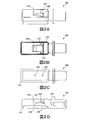
- 2A to 2D are perspective views showing the configuration of the optical receptacle according to the embodiment of the present invention.
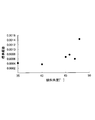
- FIG. 3 is a graph showing the relationship between the tilt angle of the optical plane and the standard deviation of the measuring device.
- FIG. 4 is a partially enlarged schematic view for explaining a method of measuring the tilt angle of the optical plane.
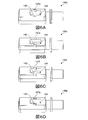
- 5A to 5C are perspective views showing a configuration of an optical receptacle according to a modification.
- 6A to 6D are perspective views showing a configuration of an optical receptacle according to a modification.
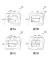
- 7A to 7D are perspective views showing a configuration of an optical receptacle according to a modification.
- 8A to 8E are perspective views showing a configuration of an optical receptacle according to a modification.
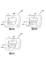
- 9A to 9C are perspective views showing a configuration of an optical receptacle according to a modification.
- 10A to 10D are perspective views showing a configuration of an optical receptacle according to a modification.
- FIG. 1 is a cross-sectional view of the optical module 100.
- FIG. 1A shows an optical path in the optical module 100 for transmission
- FIG. 1B shows an optical path in the optical module 100 for reception.
- hatching of the cross section of the optical receptacle 140 is omitted to show the optical path in the optical receptacle 140.
- the optical module 100 includes a photoelectric conversion device 120 including a substrate 121 and a photoelectric conversion element (light emitting element 122 or light receiving element 123), and an optical receptacle 140.
- the optical module 100 is used in a state where the optical transmission body 150 is connected to the optical receptacle 140 via the ferrule 152.
- the photoelectric conversion device 120 includes a substrate 121, a light emitting element 122 or a light receiving element 123, and a detection element 124.
- a light emitting element 122 is used as a photoelectric conversion element.
- a light receiving element 123 is used as a photoelectric conversion element.
- the substrate 121 is, for example, a glass composite substrate, a glass epoxy substrate, or a flexible sill substrate.
- a light emitting element 122 or a light receiving element 123 and a detection element 124 (described later) are arranged.
- the light emitting element 122 is disposed on the substrate 121, and emits laser light in a direction perpendicular to the installation portion of the substrate 121 on which the light emitting element 122 is disposed.
- the number of the light emitting elements 122 is not particularly limited. In this embodiment, the number of light emitting elements 122 is one. Further, the position of the light emitting element 122 is not particularly limited.
- the light emitting element 122 is, for example, a vertical cavity surface emitting laser (VCSEL).
- the light receiving element 123 is disposed on the substrate 121 and receives the received light Lr from the end surface 151 of the optical transmission body 150.
- the number of light receiving elements 123 is not particularly limited. In the present embodiment, the number of light receiving elements 123 is one. Further, the position of the light receiving element 123 is not particularly limited.
- the light receiving element 123 is, for example, a photo detector.
- the detection element 124 receives monitor light Lm for monitoring the output (for example, intensity and light quantity) of the emitted light L emitted from the light emitting element 122.
- the detection element 124 is, for example, a photo detector.
- the number of detection elements 124 is not particularly limited. In the present embodiment, the number of detection elements 124 is one.
- the optical receptacle 140 is disposed on the substrate 121 of the photoelectric conversion device 120.
- the optical receptacle 140 is disposed between the photoelectric conversion device 120 and the optical transmission body 150, and connects the light emitting surface 125 of the light emitting element 122 or the light receiving surface 126 of the light receiving element 123 and the end surface 151 of the optical transmission body 150. Connect optically.
- the configuration of the optical receptacle 140 will be described in detail separately.
- the type of the optical transmission body 150 is not particularly limited.
- Examples of the optical transmission body 150 include an optical fiber and an optical waveguide.
- the optical transmission body 150 is a single optical fiber.
- the optical fiber may be a single mode method or a multimode method.
- FIG. 2A to 2D are diagrams showing the configuration of the optical receptacle 140 according to Embodiment 1.
- FIG. 2A is a perspective view of the optical receptacle 140
- FIG. 2B is a plan view
- FIG. 2C is a bottom view
- FIG. 2D is a cross-sectional view.
- the optical receptacle 140 will be described with the surface to which the optical transmission body 150 is connected as the front surface and the surface facing the photoelectric conversion device 120 as the bottom surface (back surface).
- the optical receptacle 140 has a shape in which a substantially rectangular parallelepiped member and a substantially cylindrical member are joined.
- the optical receptacle 140 emits the emitted light L emitted from the light emitting surface 125 of the light emitting element 122 toward the end surface 151 of the optical transmission body 150.
- the optical receptacle 140 emits the received light Lr from the optical transmission body 150 toward the light receiving surface 126 of the light receiving element 123.
- the optical receptacle 140 includes an installation plane 141, a first optical surface 142, a reflection surface 143, a light separation unit 144, a second optical surface 145, a third optical surface 146, and a reference plane 147.
- the optical receptacle 140 is formed using a material that transmits light with a wavelength used for optical communication. Examples of such materials include transparent resins such as polyetherimide (PEI) and cyclic olefin resins.
- PEI polyetherimide
- cyclic olefin resins for example, the optical receptacle 140 is manufactured by injection molding.
- the installation plane 141 is a surface (bottom surface) that contacts the photoelectric conversion device 120 (substrate 121) when the optical receptacle 140 is installed on the substrate 121 of the photoelectric conversion device 120. As described later, in the present embodiment, the installation plane 141 serves as a reference (0 °) for the inclination angle of the optical plane of the optical receptacle 140. When the optical receptacle 140 is installed on the substrate 121 of the photoelectric conversion device 120, the installation plane 141 is parallel to the surface of the substrate 121, and the outgoing light L and reception between the reflecting surface 143 and the second optical surface 145 are received. Along the optical axis of the light Lr.
- the first optical surface 142 causes the emitted light L emitted from the light emitting element 122 to enter the inside of the optical receptacle 140 or emits the received light Lr from the optical transmission body 150 toward the light receiving element 123 from the optical receptacle 140. It is an optical surface.
- the shape of the first optical surface 142 is a convex lens surface that is convex toward the photoelectric conversion element 120.
- the first optical surface 142 converts the emitted light L emitted from the light emitting element 122 into collimated light.
- the first optical surface 142 is formed on the bottom surface of the concave portion provided on the back side (installation plane 141) of the optical receptacle 140, with the light emitting surface 125 of the light emitting element 122 or the light receiving surface 126 of the light receiving element 123. They are arranged so as to face each other. Further, the planar view shape of the first optical surface 142 is a circle.
- the central axis of the first optical surface 142 is preferably perpendicular to the light emitting surface 125 of the light emitting element 122 or the light receiving surface 126 of the light receiving element 123.
- the central axis of the first optical surface 142 is preferably coincident with the optical axis of the light emitted from the light emitting element 122 or the light incident on the light receiving element 123.
- the reflecting surface 143 reflects the light incident on the first optical surface 142 toward a second optical surface 145 (described later), or reflects the light incident on the inside of the optical receptacle 140 by the second optical surface 145 to the first optical surface.
- 142 is an optical surface (optical plane) to be reflected toward 142.
- the reflecting surface 143 is disposed on the optical path between the first optical surface 142 and the second optical surface 145.
- the reflective surface 143 is inclined so as to approach the optical transmission body 150 (front side) from the bottom surface side of the optical receptacle 140 toward the top surface side.
- the inclination angle of the reflecting surface 143 with respect to the installation plane 141 is 45 °.
- the shape of the reflective surface 143 is not particularly limited. In the present embodiment, the shape of the reflecting surface 143 is a plane. The light incident on the first optical surface 142 or the second optical surface 145 enters the reflecting surface 143 at an incident angle larger than the critical angle.
- the light separation unit 144 is configured to monitor light Lm having a predetermined light beam diameter (collimated light) L incident on the first optical surface 142 and directed to the detection element 124, and a second optical surface (end surface 151 of the optical transmission body 150). Is separated into the signal light Ls directed to.
- the light separating portion 144 is an inclined surface with respect to the optical axis of the outgoing light L that is incident on the first optical surface 142 and reflected by the reflecting surface 143. In the present embodiment, the light separating section 144 is inclined so as to approach the optical transmission body 150 (front side) from the top surface side to the bottom surface side of the optical receptacle 140.
- the light separation unit 144 reflects a part of the outgoing light L incident on the first optical surface 142 and reflected on the reflection surface 143 toward the third optical surface 146.
- the inclination angle with respect to the installation plane 141 of the light separation part 144 is not particularly limited. In the present embodiment, the inclination angle of the light separating portion 144 with respect to the installation plane 141 is 60 °.
- the light separating unit 144 has a part of the top surface side of the emitted light L that is incident on the inside of the optical receptacle 140 by the first optical surface 142 and reflected by the reflecting surface 143. Light enters at an incident angle greater than the critical angle. The light separation unit 144 reflects the incident outgoing light L toward the third optical surface 146 to generate monitor light Lm. On the other hand, a part of the light on the bottom side of the emitted light L travels toward the second optical surface 145 without entering the light separating portion 144, and the signal light Ls toward the end surface 151 of the optical transmission body 150. Become.
- the light quantity ratio between the signal light Ls and the monitor light Lm is to obtain the monitor light Lm that can monitor the intensity and the light quantity of the emitted light L emitted from the light emitting element 122 while obtaining the desired signal light Ls. If it is possible, there is no particular limitation.
- the second optical surface 145 emits the signal light Ls toward the end surface 151 of the optical transmission body 150 or refracts the reception light Lr emitted from the end surface 151 of the optical transmission body 150 to enter the optical receptacle 140. It is an optical surface.
- the plurality of second optical surfaces 145 are arranged on the front side of the optical receptacle 140 so as to face the end surface 151 of the optical transmission body 150.
- the shape of the second optical surface 145 is a convex lens surface that is convex toward the end surface of the optical transmission body 150.
- the third optical surface 146 is disposed on the bottom surface side of the optical receptacle 140 so as to face the detection element 124.
- the third optical surface 146 is a convex lens surface that is convex toward the detection element 124.
- the third optical surface 146 converges the monitor light Lm separated by the light separation unit 144 and emits it toward the detection element 124. Thereby, the monitor light Lm can be efficiently incident on the detection element 124.
- the central axis of the third optical surface 146 is preferably perpendicular to the light receiving surface 126 (substrate 121) of the detection element 124.
- the reference plane 147 is arranged at a position not on the optical path in the optical receptacle 140. Although details will be described later, the reference plane 147 has an inclination angle with respect to the installation plane 141 that is smaller than an inclination angle of an optical plane (for example, the reflection surface 143 or the light separation unit 144) with respect to the installation plane 141.
- the angle of the reference plane 147 with respect to the installation plane 141 is not particularly limited as long as it is within a range that can be measured with high accuracy by a measuring apparatus using a laser probe.
- the inclination angle of the reference plane 147 with respect to the installation plane 141 is, for example, 40 ° or less. In the present embodiment, the inclination angle of the reference plane 147 with respect to the installation plane 141 is 30 °.
- optical receptacle 140 The configuration of the optical receptacle 140 has been described above. Here, the optical path in the optical module 100 will be described.
- the outgoing light L emitted from the light emitting element 122 is incident on the inside of the optical receptacle 140 through the first optical surface 142.
- incident light is converted into collimated light by the first optical surface 142 and travels toward the reflecting surface 143.
- the incident light is reflected by the reflecting surface 143 and travels toward the light separating portion 144.
- a part of the light beam that has reached the light separation unit 144 is reflected by the light separation unit 144 that is a reflection surface, is emitted to the outside of the optical receptacle 140 by the third optical surface 146, and reaches the detection element 124 as the monitor light Lm.
- the remaining part of the light beam that has not reached the light separation unit 144 (light that has not been reflected by the light separation unit 144) reaches the end surface 151 of the optical transmission body 150 as the signal light Ls.
- the signal light Ls is condensed on the center of the end surface 151 of the optical transmission body 150 by the second optical surface 145.
- the received light Lr emitted from the end surface 151 of the optical transmission body 150 is incident on the inside of the optical receptacle 140 at the second optical surface 145.
- the received light Lr (incident light) is collected by the second optical surface 145, and the diameter of the light beam decreases as it approaches the light separator 144.
- the received light Lr reaches the reflecting surface 143 without being blocked by the light separation unit 144.
- the beam diameter of the received light Lr increases as it approaches the reflecting surface 143.
- the light reflected by the reflecting surface 143 is emitted to the outside of the optical receptacle 140 by the first optical surface 142 and reaches the light receiving element 123.
- the received light Lr (emitted light) is collected at the center of the light receiving surface 126 of the light receiving element 123 by the first optical surface 142.
- the optical receptacle was rotated using a stage capable of adjusting the angle with high accuracy so as to be 46 °, 47 °, 48 ° or 49 °. At this time, the inclination angle of the optical plane was measured using the inclination angle of the installation plane at the original position (position before rotation) as a reference (0 °).
- the optical receptacle was manufactured by injection molding using polyetherimide (PEI) as a material.
- a laser focus three-dimensional measuring machine (NH-3 manufactured by Mitaka Kogyo Co., Ltd.) was used, and the tilt angle of the optical plane with respect to the installation plane was measured by the point autofocus method (ISO 25178-605: 2014).
- the diameter of the measurement range was 0.8 mm
- the number of data points was 800 points
- the three-dimensional shape of the optical plane was measured
- the inclination angle of the optical plane with respect to the installation plane was measured based on the shape. The above measurement was performed five times for each inclination angle.
- FIG. 3 is a graph showing the relationship between the tilt angle of the optical plane and the standard deviation of the measurement results.
- the horizontal axis indicates the inclination angle (°) of the optical plane with respect to the installation plane
- the vertical axis indicates the standard deviation of five measurement results.
- the measurement result is not shown. From this result, it was found that in this measuring apparatus, when the inclination angle exceeds 40 °, the standard deviation of the measurement result increases and the measurement accuracy decreases. It was also found that the maximum measurable tilt angle was 48 °. Therefore, from the viewpoint of performing highly accurate measurement, the inclination angle of the optical plane with respect to the installation plane is preferably 40 ° or less.
- the inclination angle of the reflection surface 143 with respect to the installation plane 141 is 45 °, and the inclination angle of the light separating portion 144 with respect to the installation plane 141 is 60 °. For this reason, in this measuring apparatus, it is difficult to measure the inclination angle of the reflection surface 143 and the light separation unit 144 with respect to the installation plane 141 with high accuracy.
- FIG. 4 is a partially enlarged schematic view for explaining a method of measuring the tilt angle of the optical plane.
- FIG. 4 is a partially enlarged schematic view of a region indicated by a broken line in FIG. 2D.
- broken lines indicate parallel lines along the installation plane 141. Therefore, the inclination angle with respect to the installation plane 141 is equal to the inclination angle with respect to the parallel line.
- the tilt angle of the optical plane (light separating unit 144) with respect to the installation plane 141 is measured in two steps.
- the optical receptacle 140 is prepared and installed in the measuring device.
- the inclination angle of the installation plane 141 and the reference plane are within an angle range in which the measurement apparatus can measure the inclination angle with high accuracy (for example, a range of 0 to ⁇ 40 ° with respect to the reference plane (0 °) in the apparatus).
- the optical receptacle 140 is installed so that the inclination angle of 147 falls.
- the first inclination angle ⁇ 1 that is the inclination angle of the reference plane 147 with respect to the installation plane 141 is measured. Specifically, the inclination angle of the installation plane 141 and the inclination angle of the reference plane 147 with respect to the reference plane in the apparatus is measured by the measurement apparatus, and a difference value between these is calculated to measure the first inclination angle ⁇ 1.
- the optical receptacle 140 and the optical axis of the laser light emitted from the laser probe are relatively rotated.
- the inclination angle of the reference plane 147 and the light separation are within an angle range in which the measurement apparatus can measure the inclination angle with high accuracy (for example, a range of 0 to ⁇ 40 ° with respect to the reference plane (0 °) in the device).
- the optical receptacle 140 is rotated so that the inclination angle of the portion 144 is kept.
- the second inclination angle ⁇ 2 that is the inclination angle of the light separating portion 144 with respect to the reference plane 147 is measured. Specifically, the inclination angle of the reference plane 147 and the inclination angle of the light separation unit 144 with respect to the reference plane in the apparatus are measured by the measurement device, and a difference value between them is calculated to measure the second inclination angle ⁇ 2.
- the measured first tilt angle ⁇ 1 and second tilt angle ⁇ 2 are added together to calculate a third tilt angle ⁇ 3 that is the tilt angle of the light separating portion 144 with respect to the installation plane 141.
- the inclination angle (third inclination angle ⁇ 3) of the light separation unit 144 with respect to the installation plane 141 is 60 °, which is larger than the measurement limit of the above-described measurement apparatus.
- the inclination angle (first inclination angle ⁇ 1) of the reference plane 147 with respect to the installation plane 141 and the inclination angle (second inclination angle ⁇ 2) of the light separating portion 144 with respect to the reference plane 147 are both 30 °, The size is within a range that can be measured with high accuracy by the measuring device.
- the inclination angle of the light separating portion 144 with respect to the installation plane 141 in the optical receptacle 140 can be measured with high accuracy.
- the inclination angle of the reference plane 147 with respect to the installation plane 141 is measured, and the inclination angle of the optical plane is measured using the reference plane 147 as a reference.
- the angle of inclination of the optical plane is measured in a plurality of times within an angle range that can be measured with high accuracy.
- the reference plane 147 serving as a reference for the tilt angle can be formed integrally with the optical receptacle 140, the tilt angle of the optical plane can be measured easily and with high accuracy.
- the case where the inclination angle of the optical plane is measured in two steps has been described.
- the measurement may be performed in three or more steps. .
- the optical plane to be measured is the light separation unit 144. It is not limited to.
- the optical plane to be measured is disposed on the optical path between the first optical surface 142 and the second optical surface 145, and at least a part of the light incident on the first optical surface 142 is directed toward the second optical surface 145.
- Any plane may be used.
- the inclination angle of the reflecting surface 143 with respect to the installation plane 141 may be measured.
- the optical receptacle 140 having the two reference planes 147 has been described.
- the number of reference planes 147 is not limited to this.
- the number of reference planes 147 may be one, or may be three or more. From the viewpoint of measuring the tilt angle with high accuracy, the reference plane 147 and the optical plane are preferably adjacent to each other when measuring the tilt angle.
- FIGS. 5A to 5C and FIGS. 6A to 6D are perspective views showing configurations of optical receptacles 140a to 140g according to modified examples.
- the reference planes 147a to 147c may be arranged on the top surface side of the optical receptacle 140a with respect to the light separating portion 144.
- the concave portion including the reference planes 147a to 147c may be opened to the concave portion including the light separating portion 144 (FIG. 5A), may be opened to the side surface (FIG. 5B), or may be opened to both. (FIG. 5C).
- the reference planes 147d to 147d may be arranged on the back side of the optical receptacle 140d from the separation unit 144.
- the concave portion including the reference planes 147d to 147g may be opened to the concave portion including the light separating portion 144 (FIG. 6A), may be opened to the side surface (FIG. 6B), or may be opened to both. They may be open (FIG. 6C) or may not be open in both (FIG. 6D).
- an optical receptacle 140 that optically connects the light emitting surface 125 of one light emitting element 122 or the light receiving surface 126 of one light receiving element 123 and the end surface 151 of one optical transmission body 150 will be described.
- the optical receptacle 140 according to the present invention is not limited to this mode.
- the optical receptacle according to the present invention includes a light emitting surface of a plurality of light emitting elements or a light receiving surface of a plurality of light receiving elements. And end faces of a plurality of optical transmission bodies may be optically connected to each other.
- optical receptacles also referred to as lens arrays
- the second optical surface 145 is arranged in a line along the long side direction on the bottom surface of the recess provided on the back side of the optical receptacles 140h to 140w
- a plurality of third optical surfaces 146 are arranged in the optical receptacles 140h to 140w. It arrange
- the areas of the reflecting surface 143 'and the light separating portion 144' are larger than those of the reflecting surface 143 and the light separating portion 144 of the optical receptacle 140 according to the present embodiment.
- the light separating section of the optical receptacle may be configured as a reflection / transmission section of a lens array (optical receptacle) described in Japanese Patent Application Laid-Open No. 2012-194372. Even in such an optical receptacle that optically connects a plurality of photoelectric conversion elements and a plurality of optical transmission bodies, the position of the reference plane is not particularly limited.
- FIGS. 7A to D, FIGS. 8A to E, FIGS. 9A to C, and FIGS. 10A to 10D are perspective views showing configurations of optical receptacles 140h to 140w according to modified examples.
- the reference planes 147h to k may be arranged in the vicinity of the light separating portion 144 '.
- the recesses including the reference planes 147h to k may open to the recesses including the light separation part 144 ′ on both sides of the recesses including the light separation part 144 ′ (FIG. 7A) or open to the side surfaces. It may be open (FIG. 7B), may be open to both (FIG. 7C), or may be disposed inside the recess including the light separating portion 144 ′ (FIG. 7D).
- the reference planes 147l to 147p may be arranged on the top surface side of the optical receptacle 140l with respect to the light separating portion 144 '.
- the concave portion including the reference planes 147l to 147p may be opened to the concave portion including the light separating portion 144 ′ on both sides of the concave portion including the light separating portion 144 ′ (FIG. 8A) or open to the side surface. May be open (FIG. 8B), may be open to both (FIG. 8C), may not be open to both (FIG. 8D), or inside the recess including the light separating portion 144 ′. It may be arranged (FIG. 8E).
- the reference planes 147q to s may be arranged on the back side of the optical receptacle 140q with respect to the light separating portion 144 '.
- the recess including the reference planes 147q to s may be opened on both the side surface and the back surface (FIG. 9A), or may be opened only on the back surface (FIGS. 9B and 9C).
- the reference plane 147s may be one.
- the recesses including the reference planes 147t to w do not have to have a bottom surface parallel to the installation plane 141.
- the concave portion including the reference planes 147t to 147w may be opened to the concave portion including the light separating portion 144 ′ on both sides of the concave portion including the light separating portion 144 ′ (FIG. 10A) or open to the side surface. It may be open (FIG. 10B), may be open to both (FIG. 10C), or may be disposed inside the recess including the light separating portion 144 ′ (FIG. 10D).
- the measurement method according to the present invention is useful, for example, for quality control when manufacturing an optical receptacle.
- Optical module 120 Photoelectric conversion device 121 Substrate 122 Light emitting element 123 Light receiving element 124 Detection element 125 Light emitting surface 126 Light receiving surface 140, 140a-w Optical receptacle 141 Installation plane 142 First optical surface 143, 143 'Reflecting surface 144, 144' Light Separator 145 Second optical surface 146 Third optical surface 147, 147a-w Reference plane 150 Optical transmission body 151 End surface 152 Ferrule L Emission light Lm Monitor light Ls Signal light Lr Reception light ⁇ 1 First inclination angle ⁇ 2 Second inclination angle ⁇ 3 Third tilt angle
Landscapes
- Physics & Mathematics (AREA)
- General Physics & Mathematics (AREA)
- Optics & Photonics (AREA)
- Optical Couplings Of Light Guides (AREA)
- Light Receiving Elements (AREA)
- Length Measuring Devices By Optical Means (AREA)
Abstract
設置平面(141)と、光学平面と、基準平面(147)とを有する光レセプタクル(140)を準備する。設置平面(141)に対する基準平面(147)の傾斜角度は、設置平面(141)に対する光学平面の傾斜角度よりも小さい。次いで、設置平面(141)に対する基準平面(147)の傾斜角度である第1傾斜角度θ1と、基準平面(147)に対する光学平面の傾斜角度である第2傾斜角度θ2とを測定する。次いで、第1傾斜角度θ1および第2傾斜角度θ2を足して設置平面(141)に対する光学平面の傾斜角度である第3傾斜角度θ3を算出する。
Description
本発明は、光レセプタクルにおける、設置平面に対する光学平面の傾斜角度を測定する方法、およびこの測定方法で光学平面の傾斜角度を測定されうる光レセプタクルに関する。
従来、光ファイバーや光導波路などの光伝送体を用いた光通信には、面発光レーザー(例えば、VCSEL:Vertical Cavity Surface Emitting Laser)などの発光素子を備えた光モジュールが使用されている。光モジュールは、発光素子から出射された通信情報を含む光を、光伝送体の端面に入射させる光レセプタクルを有する。
また、光モジュールには、温度変化に対する発光素子の出力特性の安定化や光出力の調整を目的として、発光素子から出射された光の強度や光量を監視(モニター)するための検出素子を有するものがある(例えば、特許文献1参照)。
特許文献1には、発光素子および検出素子(受光素子)を含む光電変換装置と、発光素子と光伝送体(光ファイバー)の端面とを光学的に接続させる光レセプタクルとを有する光モジュールが記載されている。また、特許文献1に記載の光レセプタクルは、発光素子から出射された光を入射させ、かつ受光素子に向けてモニター光を出射する第1の面と、発光素子から出射され、第1の面で入射した光を反射させる第1の反射面と、第1の反射面で反射された光を、第1の面に向かうモニター光と、光ファイバーの端面に結合すべき光(信号光)とに分離する光分離部と、光分離部によって分離された光を光ファイバーの端面に向けて出射する第2の面と、を有する。
特許文献1に記載の光モジュールでは、発光素子から出射され、第1の面で入射した光は、第1の反射面で反射されて、光分離部に向かって進行する。光分離部に到達した光は、光分離部で信号光およびモニター光に分離される。モニター光は、受光素子の受光面に向けて第1の面から出射される。一方、信号光は、光ファイバーの受光面に向けて第2の面から出射される。
光レセプタクルにおいて、光が透過または反射する光学平面は、光の送受信に影響を及ぼすため、その傾斜角度は、高精度に制御される必要があり、光学平面の傾斜角度は、高精度に測定される必要がある。光レセプタクルの光学平面の傾斜角度を高精度に測定できる方法として、測定対象物の形状を、レーザープローブを用いて非接触式で測定する方法が知られている(例えば、特許文献2参照)。
特許文献2には、ステージ走査型レーザープローブ方式で測定対象物の形状を測定するための方法および装置が記載されている。特許文献2に記載の測定装置は、レーザー光照射手段、対物レンズ、フォーカス手段、センサー、AF(Auto Focus)スケール、XステージおよびYステージを有する。まず、測定対象物(測定ワーク)をYステージ上に配置されたXステージの上に配置する。次いで、レーザー光照射手段により、対物レンズを介して測定対象物にレーザー光を照射させる。次いで、測定対象物で反射し、再び対物レンズを通ってきた反射光をセンサー上に結像させる。このとき、フォーカスが合っていなければ、フォーカス手段が対物レンズのZ軸方向における位置をフォーカスポイントまで移動させる。このとき、AFスケールは、対物レンズの位置(移動量)を検出する。このように、検出された各ポイントのXYZの座標値に基づいて、測定対象物の形状を測定することができる。
しかしながら、前述のとおり、特許文献2に記載の測定方法では、測定対象物で反射した光が再び対物レンズを通り、センサー上に到達しなければ測定することができない。このため、光レセプタクルにおける光学平面の傾斜角度を測定する場合であって、光学平面の傾斜角度が所定の角度より大きいときには、光学平面で反射した光が適切にセンサーに戻らず、結果として、測定精度が低下してしまうか、または測定不能となってしまうことがある。
そこで、本発明の目的は、光レセプタクルにおける、設置平面に対する光学平面の傾斜角度を、レーザープローブを用いて非接触式で測定する方法であって、設置平面に対する光学平面の傾斜角度が大きい場合であっても、光学平面の傾斜角度を高精度に測定できる測定方法を提供することである。また、本発明の別の目的は、当該測定方法で光学平面の傾斜角度を測定されうる光レセプタクルを提供することである。
本発明に係る測定方法は、光レセプタクルにおける、設置平面に対する光学平面の傾斜角度を、レーザープローブを用いて非接触式で測定する方法であって、設置平面と、光学平面と、前記設置平面に対するその傾斜角度が前記設置平面に対する前記光学平面の傾斜角度よりも小さい基準平面とを有する光レセプタクルを準備する工程と、前記設置平面に対する前記基準平面の傾斜角度である第1傾斜角度を測定する工程と、前記基準平面に対する前記光学平面の傾斜角度である第2傾斜角度を測定する工程と、前記第1傾斜角度および前記第2傾斜角度を足して前記設置平面に対する前記光学平面の傾斜角度である第3傾斜角度を算出する工程と、を有する。
本発明に係る光レセプタクルは、基板および前記基板上に配置された1または2以上の光電変換素子を含む光電変換装置と、1または2以上の光伝送体との間に設置され、前記光電変換素子と前記光伝送体の端面とを光学的に結合するための光レセプタクルであって、前記光レセプタクルが前記光電変換装置の前記基板上に設置されたときに前記基板に接触する面である設置平面と、前記光電変換素子から出射された光を入射させるか、前記光伝送体の端面から出射され、前記光レセプタクルの内部を通る光を前記光電変換素子に向けて出射させる、1または2以上の第1光学面と、前記第1光学面で入射した光を前記光伝送体の端面に向けて出射させるか、前記光伝送体の端面から出射された光を入射させる、1または2以上の第2光学面と、前記第1光学面および前記第2光学面の間の光路上に配置され、前記第1光学面で入射した光の少なくとも一部を前記第2光学面に向けて透過または反射させ、あるいは前記第2光学面で入射した光の少なくとも一部を前記第1光学面に向けて透過または反射させる、前記設置平面に対して40°より大きい角度で傾斜している光学平面と、前記光レセプタクル内における光路上ではない位置に配置され、前記設置平面に対するその傾斜角度が前記設置平面に対する前記光学平面の傾斜角度よりも小さい基準平面と、を有する。
本発明によれば、設置平面に対する光学平面の傾斜角度が大きい場合であっても、光学平面の傾斜角度を高精度に測定することができる。したがって、本発明によれば、光レセプタクルの光学設計の自由度が広がり、より複雑な光学製品を高精度に設計および製造することができる。さらに、従来の測定装置を使用して、より高精度に光学平面の傾斜角度を測定することができるため、測定コストおよび製造コストの増加を抑制することができる。
以下、本発明に係る一実施の形態について、図面を参照して詳細に説明する。
(光モジュールの構成)
図1は、光モジュール100の断面図である。図1Aには、送信用の光モジュール100における光路を示しており、図1Bには、受信用の光モジュール100における光路を示している。なお、図1Aおよび図1Bでは、光レセプタクル140内の光路を示すために光レセプタクル140の断面へのハッチングを省略している。
図1は、光モジュール100の断面図である。図1Aには、送信用の光モジュール100における光路を示しており、図1Bには、受信用の光モジュール100における光路を示している。なお、図1Aおよび図1Bでは、光レセプタクル140内の光路を示すために光レセプタクル140の断面へのハッチングを省略している。
図1Aおよび図1Bに示されるように、光モジュール100は、基板121および光電変換素子(発光素子122または受光素子123)を含む光電変換装置120と、光レセプタクル140と、を有する。光モジュール100は、光レセプタクル140に光伝送体150がフェルール152を介して接続された状態で使用される。
光電変換装置120は、基板121と、発光素子122または受光素子123と、検出素子124と、を有する。送信用の光モジュール100では、光電変換素子として発光素子122が使用される。受信用の光モジュール100では、光電変換素子として受光素子123が使用される。基板121は、例えば、ガラスコンポジット基板やガラスエポキシ基板、フレキブシル基板などである。基板121上には、発光素子122または受光素子123と、検出素子124(後述)とが配置されている。
発光素子122は、基板121上に配置され、発光素子122が配置された基板121の設置部に対して垂直方向にレーザー光を出射する。発光素子122の数は、特に限定されない。本実施の形態では、発光素子122の数は、1個である。また、発光素子122の位置も特に限定されない。発光素子122は、例えば、垂直共振器面発光レーザー(VCSEL)である。
受光素子123は、基板121上に配置され、光伝送体150の端面151からの受信光Lrを受光する。受光素子123の数は、特に限定されない。本実施の形態では、受光素子123の数は、1個である。また、受光素子123の位置も特に限定されない。受光素子123は、例えば、フォトディテクターである。
検出素子124は、発光素子122から出射された出射光Lの出力(例えば、強度や光量)を監視するためのモニター光Lmを受光する。検出素子124は、例えば、フォトディテクターである。検出素子124の数は、特に限定されない。本実施の形態では、検出素子124の数は、1個である。
光レセプタクル140は、光電変換装置120の基板121上に配置されている。光レセプタクル140は、光電変換装置120と光伝送体150との間に配置された状態で、発光素子122の発光面125または受光素子123の受光面126と、光伝送体150の端面151とを光学的に接続させる。光レセプタクル140の構成については、別途詳細に説明する。
光伝送体150の種類は、特に限定されない。光伝送体150の例には、光ファイバー、光導波路などが含まれる。本実施の形態では、光伝送体150は、1本の光ファイバーである。光ファイバーは、シングルモード方式であってもよいし、マルチモード方式であってもよい。
(光レセプタクルの構成)
図2A~Dは、実施の形態1に係る光レセプタクル140の構成を示す図である。図2Aは、光レセプタクル140の斜視図であり、図2Bは、平面図であり、図2Cは、底面図であり、図2Dは、断面図である。以下、光レセプタクル140について、光伝送体150が接続される側の面を正面とし、光電変換装置120と対向する面を底面(裏面)として説明する。
図2A~Dは、実施の形態1に係る光レセプタクル140の構成を示す図である。図2Aは、光レセプタクル140の斜視図であり、図2Bは、平面図であり、図2Cは、底面図であり、図2Dは、断面図である。以下、光レセプタクル140について、光伝送体150が接続される側の面を正面とし、光電変換装置120と対向する面を底面(裏面)として説明する。
図1A、Bおよび図2A~Dに示されるように、光レセプタクル140は、略直方体形状の部材と略円筒形状の部材とを接合した形状である。送信用の光モジュール100では、光レセプタクル140は、発光素子122の発光面125から出射された出射光Lを光伝送体150の端面151に向けて出射させる。受信用の光モジュール100では、光レセプタクル140は、光伝送体150からの受信光Lrを受光素子123の受光面126に向けて出射させる。光レセプタクル140は、設置平面141、第1光学面142、反射面143、光分離部144、第2光学面145、第3光学面146および基準平面147を有する。光レセプタクル140は、光通信に用いられる波長の光に対して透光性を有する材料を用いて形成される。そのような材料の例には、ポリエーテルイミド(PEI)や環状オレフィン樹脂などの透明な樹脂が含まれる。また、例えば、光レセプタクル140は、射出成形により製造される。
設置平面141は、光レセプタクル140が光電変換装置120の基板上121に設置されたときに、光電変換装置120(基板121)に接触する面(底面)である。後述のとおり、本実施の形態では、設置平面141は、光レセプタクル140の光学平面の傾斜角度についての基準(0°)となる。光レセプタクル140が光電変換装置120の基板121上に設置されている場合、設置平面141は、基板121面と平行であり、反射面143と第2光学面145との間の出射光Lおよび受信光Lrの光軸に沿う。
第1光学面142は、発光素子122から出射された出射光Lを光レセプタクル140の内部に入射させるか、光伝送体150からの受信光Lrを光レセプタクル140から受光素子123に向けて出射させる光学面である。本実施の形態では、第1光学面142の形状は、光電変換素子120に向かって凸状の凸レンズ面である。第1光学面142は、発光素子122から出射された出射光Lをコリメート光に変換させる。また、本実施の形態では、第1光学面142は、光レセプタクル140の裏側(設置平面141)に設けられた凹部の底面に、発光素子122の発光面125または受光素子123の受光面126とそれぞれ対向するように配置されている。また、第1光学面142の平面視形状は、円形である。第1光学面142の中心軸は、発光素子122の発光面125または受光素子123の受光面126に対して垂直であることが好ましい。また、第1光学面142の中心軸は、発光素子122から出射された光、または受光素子123に入射する光の光軸と一致することが好ましい。
反射面143は、第1光学面142で入射した光を第2光学面145(後述)に向けて反射させるか、第2光学面145で光レセプタクル140の内部に入射した光を第1光学面142に向けて反射させる光学面(光学平面)である。反射面143は、第1光学面142および第2光学面145の間の光路上に配置されている。反射面143は、光レセプタクル140の底面側から天面側に向かうにつれて、光伝送体150(正面側)に近づくように傾斜している。本実施の形態では、設置平面141に対する反射面143の傾斜角度は、45°である。反射面143の形状は、特に限定されない。本実施の形態では、反射面143の形状は、平面である。反射面143には、第1光学面142または第2光学面145で入射した光が、臨界角より大きな入射角で入射する。
光分離部144は、第1光学面142で入射した所定の光束径の出射光(コリメート光)Lを検出素子124に向かうモニター光Lmと、第2光学面(光伝送体150の端面151)に向かう信号光Lsとに分離させる。光分離部144は、第1光学面142で入射し、反射面143で反射された出射光Lの光軸に対する傾斜面である。本実施の形態では、光分離部144は、光レセプタクル140の天面側から底面側に向かうにつれて光伝送体150(正面側)に近づくように傾斜している。これにより、光分離部144は、第1光学面142で入射し、反射面143で反射された出射光Lの一部を第3光学面146に向けて反射させる。また、光分離部144の設置平面141に対する傾斜角度は、特に限定されない。本実施の形態では、光分離部144の設置平面141に対する傾斜角度は、60°である。
図1Aに示されるように、光分離部144には、第1光学面142で光レセプタクル140の内部に入射し、反射面143で反射された出射光Lのうちの天面側の一部の光が、臨界角より大きな入射角で入射する。光分離部144は、入射した出射光Lを第3光学面146に向けて反射させて、モニター光Lmを生成する。一方、出射光Lのうちの底面側の一部の光は、光分離部144に入射することなく第2光学面145に向かって進行し、光伝送体150の端面151に向かう信号光Lsとなる。
信号光Lsとモニター光Lmとの光量比は、所望の光量の信号光Lsを得つつ、発光素子122から出射された出射光Lの強度や光量を監視することができるモニター光Lmを得ることができれば、特に限定されない。信号光Lsとモニター光Lmとの光量比は、信号光Ls:モニター光Lm=6:4~8:2であることが好ましく、信号光Ls:モニター光Lm=7:3であることがさらに好ましい。光分離部144に入射する出射光Lの光量を調整することで、信号光Lsと、モニター光Lmとの光量比を調整することができる。
第2光学面145は、信号光Lsを光伝送体150の端面151に向けて出射させるか、光伝送体150の端面151から出射された受信光Lrを屈折させて光レセプタクル140の内部に入射させる光学面である。本実施の形態では、複数の第2光学面145は、光レセプタクル140の正面側に、光伝送体150の端面151と対向するように配置されている。第2光学面145の形状は、光伝送体150の端面に向かって凸状の凸レンズ面である。これにより、光分離部144で分離された信号光Lsを集光させて、光伝送体150の端面151に効率良く入射させることができる。また、光伝送体150から出射された受信光Lrも、収束させることで、光分離部144に進行を妨げられることなく、反射面143に到達させることができる。
第3光学面146は、光レセプタクル140の底面側に、検出素子124と対向するように配置されている。本実施の形態では、第3光学面146は、検出素子124に向かって凸状の凸レンズ面である。第3光学面146は、光分離部144で分離されたモニター光Lmを収束させて検出素子124に向けて出射させる。これにより、モニター光Lmを検出素子124に効率良く入射させることができる。第3光学面146の中心軸は、検出素子124の受光面126(基板121)に対して垂直であることが好ましい。
基準平面147は、光レセプタクル140内における光路上ではない位置に配置されている。詳細については後述するが、基準平面147は、設置平面141に対するその傾斜角度が、設置平面141に対する光学平面(例えば、反射面143または光分離部144)の傾斜角度よりも小さい。設置平面141に対する基準平面147の角度は、レーザープローブを用いた測定装置によって高精度に測定されうる範囲内であれば特に限定されない。基準平面147の設置平面141に対する傾斜角度は、例えば、40°以下である。本実施の形態では、設置平面141に対する基準平面147の傾斜角度は、30°である。
以上、光レセプタクル140の構成について説明した。ここで、光モジュール100における光路について説明する。
図1Aに示されるように、送信用の光モジュール100では、発光素子122から出射された出射光Lは、第1光学面142で光レセプタクル140の内部に入射する。このとき、入射光は、第1光学面142によってコリメート光に変換され、反射面143に向かって進行する。次いで、入射光は、反射面143で反射され、光分離部144に向かって進行する。光分離部144に到達した光束の一部は、反射面である光分離部144で反射され、第3光学面146で光レセプタクル140の外部に出射されて、モニター光Lmとして検出素子124に到達する。一方、光分離部144に到達しなかった光束の残部(光分離部144で反射されなかった光)は、信号光Lsとして光伝送体150の端面151に到達する。このとき、信号光Lsは、第2光学面145によって光伝送体150の端面151の中心に集光される。
図1Bに示されるように、受信用の光モジュール100では、光伝送体150の端面151から出射された受信光Lrは、第2光学面145で光レセプタクル140の内部に入射する。受信光Lr(入射光)は、第2光学面145によって集光され、光分離部144に近づくにつれて光束径が小さくなる。これにより、受信光Lrは、光分離部144に進行を妨げられることなく、反射面143に到達する。このとき、受信光Lrは、反射面143に近づくにつれて光束径が大きくなる。次いで、反射面143で反射された光は、第1光学面142で光レセプタクル140の外部に出射され、受光素子123に到達する。このとき、受信光Lr(出射光)は、第1光学面142によって、受光素子123の受光面126の中心に集光される。
(光学平面の傾斜角度の測定)
次に、本実施の形態に係る光レセプタクル140において、設置平面141に対する光学平面の傾斜角度を測定するための方法について説明する。本実施の形態では、光学平面として、設置平面141に対する光分離部144の傾斜角度(設計角度:60°)を測定する。本実施の形態に係る測定方法では、レーザープローブを用いて非接触形式で測定するための測定装置を用いる。そこで、先に測定装置の測定精度について説明し、その後に測定方法について説明する。
次に、本実施の形態に係る光レセプタクル140において、設置平面141に対する光学平面の傾斜角度を測定するための方法について説明する。本実施の形態では、光学平面として、設置平面141に対する光分離部144の傾斜角度(設計角度:60°)を測定する。本実施の形態に係る測定方法では、レーザープローブを用いて非接触形式で測定するための測定装置を用いる。そこで、先に測定装置の測定精度について説明し、その後に測定方法について説明する。
(1)測定装置の測定精度
光レセプタクルの光学平面の傾斜角度を測定するための測定装置について、光学平面の傾斜角度と、測定装置の測定精度との関係について調べた。なお、本実験では、設置平面に対する光学平面の傾斜角度が35°、40°、45°、46°、47°、48°または49°である場合について測定を行った。光レセプタクルとしては、設置平面に対する傾斜角度が45°である光学平面を有する光レセプタクルを使用した。そして、設置平面に対する光学平面の傾斜角度が45°以外である場合について測定するときは、元の位置(回転前の位置)の設置平面に対して光学平面の傾斜角度が35°、40°、46°、47°、48°または49°となるように、高精度で角度調整可能なステージを用いて光レセプタクルを回転させた。このとき、元の位置(回転前の位置)の設置平面の傾斜角度を基準(0°)として光学平面の傾斜角度を測定した。光レセプタクルは、ポリエーテルイミド(PEI)を材料として、射出成形により製造した。測定装置として、レーザーフォーカス三次元測定機(三鷹光器株式会社製NH-3)を使用し、ポイントオートフォーカス法(ISO 25178-605:2014)により設置平面に対する光学平面の傾斜角度を測定した。このとき、測定範囲の直径を0.8mm、データ点数を800点として、光学平面の3次元形状を測定し、当該形状に基づいて設置平面に対する光学平面の傾斜角度を測定した。各傾斜角度について、上記の測定を5回ずつ行った。
光レセプタクルの光学平面の傾斜角度を測定するための測定装置について、光学平面の傾斜角度と、測定装置の測定精度との関係について調べた。なお、本実験では、設置平面に対する光学平面の傾斜角度が35°、40°、45°、46°、47°、48°または49°である場合について測定を行った。光レセプタクルとしては、設置平面に対する傾斜角度が45°である光学平面を有する光レセプタクルを使用した。そして、設置平面に対する光学平面の傾斜角度が45°以外である場合について測定するときは、元の位置(回転前の位置)の設置平面に対して光学平面の傾斜角度が35°、40°、46°、47°、48°または49°となるように、高精度で角度調整可能なステージを用いて光レセプタクルを回転させた。このとき、元の位置(回転前の位置)の設置平面の傾斜角度を基準(0°)として光学平面の傾斜角度を測定した。光レセプタクルは、ポリエーテルイミド(PEI)を材料として、射出成形により製造した。測定装置として、レーザーフォーカス三次元測定機(三鷹光器株式会社製NH-3)を使用し、ポイントオートフォーカス法(ISO 25178-605:2014)により設置平面に対する光学平面の傾斜角度を測定した。このとき、測定範囲の直径を0.8mm、データ点数を800点として、光学平面の3次元形状を測定し、当該形状に基づいて設置平面に対する光学平面の傾斜角度を測定した。各傾斜角度について、上記の測定を5回ずつ行った。
図3は、光学平面の傾斜角度と、測定結果の標準偏差との関係を示すグラフである。図3において、横軸は、設置平面に対する光学平面の傾斜角度(°)を示し、縦軸は、5回の測定結果の標準偏差を示す。なお、傾斜角度が49°の光学平面については、装置の測定限界により測定できなかったため、測定結果を示していない。この結果から、この測定装置では、傾斜角度が40°を超えると、測定結果の標準偏差が増加し、測定精度が低下することがわかった。また、測定可能な限界の傾斜角度が48°であることもわかった。したがって、高精度な測定を行う観点から、設置平面に対する光学平面の傾斜角度は、40°以下であることが好ましい。
本実施の形態に係る光レセプタクル140では、設置平面141に対する反射面143の傾斜角度は45°であり、設置平面141に対する光分離部144の傾斜角度は60°である。このため、この測定装置では、設置平面141に対する反射面143および光分離部144の傾斜角度を高精度に測定することは困難である。
(2)光学平面の傾斜角度の測定方法
次に、本実施の形態に係る光学平面の傾斜角度の測定方法について説明する。図4は、光学平面の傾斜角度の測定方法を説明するための部分拡大模式図である。図4は、図2Dにおいて破線で示される領域の部分拡大模式図である。図4において、破線は、設置平面141に沿う平行線を示している。したがって、設置平面141に対する傾斜角度は、当該平行線に対する傾斜角度に等しい。また、本実施の形態に係る光学平面の傾斜角度の測定方法では、設置平面141に対する光学平面(光分離部144)の傾斜角度を2回に分けて測定する。
次に、本実施の形態に係る光学平面の傾斜角度の測定方法について説明する。図4は、光学平面の傾斜角度の測定方法を説明するための部分拡大模式図である。図4は、図2Dにおいて破線で示される領域の部分拡大模式図である。図4において、破線は、設置平面141に沿う平行線を示している。したがって、設置平面141に対する傾斜角度は、当該平行線に対する傾斜角度に等しい。また、本実施の形態に係る光学平面の傾斜角度の測定方法では、設置平面141に対する光学平面(光分離部144)の傾斜角度を2回に分けて測定する。
まず、光レセプタクル140を準備して測定装置に設置する。このとき、測定装置が高精度に傾斜角度を測定できる角度範囲(例えば、装置における基準面(0°)に対して0~±40°の範囲)内に、設置平面141の傾斜角度および基準平面147の傾斜角度が収まるように、光レセプタクル140を設置する。
次いで、設置平面141に対する基準平面147の傾斜角度である第1傾斜角度θ1を測定する。具体的には、測定装置により、装置における基準面に対する設置平面141の傾斜角度および基準平面147の傾斜角度を測定し、これらの差分値を算出して第1傾斜角度θ1を測定する。
次いで、光レセプタクル140と、レーザープローブから放出されるレーザー光の光軸とを相対的に回転させる。このとき、測定装置が高精度に傾斜角度を測定できる角度範囲(例えば、装置における基準面(0°)に対して0~±40°の範囲)内に、基準平面147の傾斜角度および光分離部144の傾斜角度が収まるように、光レセプタクル140を回転させる。
次いで、基準平面147に対する光分離部144の傾斜角度である第2傾斜角度θ2を測定する。具体的には、測定装置により、装置における基準面に対する基準平面147の傾斜角度および光分離部144の傾斜角度を測定し、これらの差分値を算出して第2傾斜角度θ2を測定する。
最後に、測定した第1傾斜角度θ1および第2傾斜角度θ2を足し合わせて、設置平面141に対する光分離部144の傾斜角度である第3傾斜角度θ3を算出する。
前述のとおり、本実施の形態に係る光レセプタクル140では、設置平面141に対する光分離部144の傾斜角度(第3傾斜角度θ3)は、60°であり、上記の測定装置の測定限界より大きい。しかしながら、設置平面141に対する基準平面147の傾斜角度(第1傾斜角度θ1)と、基準平面147に対する光分離部144の傾斜角度(第2傾斜角度θ2)とは、ともに30°であり、上記の測定装置により高精度に測定できる範囲内の大きさである。したがって、上記の手順により、測定装置の測定限界より大きい傾斜角度であったとしても、光レセプタクル140における、設置平面141に対する光分離部144の傾斜角度を高精度で測定することができる。
(効果)
以上のように、本実施の形態に係る測定方法では、設置平面141に対する基準平面147の傾斜角度を測定し、当該基準平面147を基準として光学平面の傾斜角度を測定する。このように、高精度で測定することができる角度範囲内で、複数回に分けて光学平面の傾斜角度の測定を行う。結果として、1回の測定では、レーザープローブ方式の測定装置を使用して適切に測定することができない傾斜角度の光学平面であっても、高精度で傾斜角度を測定することができる。
以上のように、本実施の形態に係る測定方法では、設置平面141に対する基準平面147の傾斜角度を測定し、当該基準平面147を基準として光学平面の傾斜角度を測定する。このように、高精度で測定することができる角度範囲内で、複数回に分けて光学平面の傾斜角度の測定を行う。結果として、1回の測定では、レーザープローブ方式の測定装置を使用して適切に測定することができない傾斜角度の光学平面であっても、高精度で傾斜角度を測定することができる。
また、傾斜角度の基準となる基準平面147は、光レセプタクル140と一体化として、形成することができるため、簡単かつ高精度で光学平面の傾斜角度を測定することができる。
なお、本実施の形態に係る測定方法では、光学平面の傾斜角度を2回に分けて測定する場合について説明したが、本発明に係る測定方法では、3回以上に分けて測定してもよい。
また、本実施の形態に係る測定方法では、光学平面として光分離部144の傾斜角度を測定する場合について説明したが、本発明に係る測定方法では、測定対象となる光学平面は光分離部144に限定されない。測定対象となる光学平面は、第1光学面142および第2光学面145の間の光路上に配置され、第1光学面142で入射した光の少なくとも一部を第2光学面145に向けて透過または反射させ、あるいは第2光学面145で入射した光の少なくとも一部を第1光学面142に向けて透過または反射させる、設置平面141に対して40°より大きい角度で傾斜している光学平面であればよい。たとえば、設置平面141に対する反射面143の傾斜角度を測定してもよい。
また、本実施の形態では、2つの基準平面147を有する光レセプタクル140について説明したが、基準平面147の数は、これに限定されない。たとえば、基準平面147の数は、1つであってもよいし、3つ以上であってもよい。傾斜角度を高精度で測定する観点から、傾斜角度の測定時において、基準平面147と、光学平面とは、隣接していることが好ましい。
(変形例)
本実施の形態では、図2Aに示されるように、2つの基準平面147が光分離部144の両側に隣接するように配置されている光レセプタクル140について説明したが、基準平面の位置は、これに限定されない。図5A~C、図6A~Dは、変形例に係る光レセプタクル140a~140gの構成を示す斜視図である。
本実施の形態では、図2Aに示されるように、2つの基準平面147が光分離部144の両側に隣接するように配置されている光レセプタクル140について説明したが、基準平面の位置は、これに限定されない。図5A~C、図6A~Dは、変形例に係る光レセプタクル140a~140gの構成を示す斜視図である。
図5A~Cに示されるように、基準平面147a~cは、光分離部144より光レセプタクル140aの天面側に配置されていてもよい。このとき、基準平面147a~cを含む凹部は、光分離部144を含む凹部に開口していてもよいし(図5A)、側面に開口していてもよいし(図5B)、両方に開口していてもよい(図5C)。
また、図6A~Dに示されるように、基準平面147d~gは、分離部144より光レセプタクル140dの背面側に配置されていてもよい。このとき、基準平面147d~gを含む凹部は、光分離部144を含む凹部に開口していてもよいし(図6A)、側面に開口していてもよいし(図6B)、両方に開口していてもよいし(図6C)、両方に開口していなくてもよい(図6D)。
さらに、本実施の形態では、1つの発光素子122の発光面125または1つの受光素子123の受光面126と、1つの光伝送体150の端面151とを光学的に接続させる光レセプタクル140について説明したが、本発明に係る光レセプタクル140は、この態様に限定されない。たとえば、図7A~D、図8A~E、図9A~C、図10A~Dに示されるように、本発明に係る光レセプタクルは、複数の発光素子の発光面または複数の受光素子の受光面と、複数の光伝送体の端面とをそれぞれ光学的に接続させてもよい。
特に図示しないが、複数の光電変換素子と、複数の光伝送体の端面とをそれぞれ光学的に接続させる光レセプタクル(レンズアレイともいう)140h~140wでは、複数の第1光学面142と、複数の第2光学面145とが、光レセプタクル140h~140wの裏側に設けられた凹部の底面に長辺方向に沿って一列に配置され、複数の第3光学面146が、光レセプタクル140h~140wの正面側に設けられた凹部の底面に長辺方向に沿って一列に配置されている。このため、光レセプタクル140h~140wでは、本実施の形態に係る光レセプタクル140の反射面143および光分離部144と比較して、反射面143’および光分離部144’の面積が、より大きい。また、光レセプタクルの光分離部は、特開2012-194372号公報に記載されているレンズアレイ(光レセプタクル)の反射/透過部のような構成であってもよい。このような複数の光電変換素子と、複数の光伝送体とをそれぞれ光学的に接続させる光レセプタクルであっても、基準平面の位置は、特に限定されない。図7A~D、図8A~E、図9A~C、図10A~Dは、変形例に係る光レセプタクル140h~140wの構成を示す斜視図である。
図7A~Dに示されるように、基準平面147h~kは、光分離部144’の近傍に配置されていてもよい。このとき、基準平面147h~kを含む凹部は、光分離部144’を含む凹部の両側において、光分離部144’を含む凹部に開口していてもよいし(図7A)、側面に開口していてもよいし(図7B)、両方に開口していてもよいし(図7C)、光分離部144’を含む凹部の内側に配置されていてもよい(図7D)。
また、図8A~Eに示されるように、基準平面147l~pは、光分離部144’より光レセプタクル140lの天面側に配置されていてもよい。このとき、基準平面147l~pを含む凹部は、光分離部144’を含む凹部の両側において、光分離部144’を含む凹部に開口していてもよいし(図8A)、側面に開口していてもよいし(図8B)、両方に開口していてもよいし(図8C)、両方に開口していなくてもよいし(図8D)、光分離部144’を含む凹部の内側に配置されていてもよい(図8E)。
また、図9A~Cに示されるように、基準平面147q~sは、光分離部144’より光レセプタクル140qの背面側に配置されていてもよい。このとき、基準平面147q~sを含む凹部は、側面および背面の両方に開口していてもよいし(図9A)、背面のみに開口していてもよいし(図9Bおよび図9C)。また、図9Cに示されるように、基準平面147sは、1つであってもよい。
また、図10A~Dに示されるように、基準平面147t~wを含む凹部は、設置平面141と平行な底面を有していなくてもよい。このとき、基準平面147t~wを含む凹部は、光分離部144’を含む凹部の両側において、光分離部144’を含む凹部に開口していてもよいし(図10A)、側面に開口していてもよいし(図10B)、両方に開口していてもよいし(図10C)、光分離部144’を含む凹部の内側に配置されていてもよい(図10D)。
本出願は、2014年12月25日出願の特願2014-263393に基づく優先権を主張する。当該出願明細書および図面に記載された内容は、すべて本願明細書に援用される。
本発明に係る測定方法は、例えば、光レセプタクルを製造する際の品質管理などに有用である。
100 光モジュール
120 光電変換装置
121 基板
122 発光素子
123 受光素子
124 検出素子
125 発光面
126 受光面
140、140a~w 光レセプタクル
141 設置平面
142 第1光学面
143、143’ 反射面
144、144’ 光分離部
145 第2光学面
146 第3光学面
147、147a~w 基準平面
150 光伝送体
151 端面
152 フェルール
L 出射光
Lm モニター光
Ls 信号光
Lr 受信光
θ1 第1傾斜角度
θ2 第2傾斜角度
θ3 第3傾斜角度
120 光電変換装置
121 基板
122 発光素子
123 受光素子
124 検出素子
125 発光面
126 受光面
140、140a~w 光レセプタクル
141 設置平面
142 第1光学面
143、143’ 反射面
144、144’ 光分離部
145 第2光学面
146 第3光学面
147、147a~w 基準平面
150 光伝送体
151 端面
152 フェルール
L 出射光
Lm モニター光
Ls 信号光
Lr 受信光
θ1 第1傾斜角度
θ2 第2傾斜角度
θ3 第3傾斜角度
Claims (8)
- 光レセプタクルにおける、設置平面に対する光学平面の傾斜角度を、レーザープローブを用いて非接触式で測定する方法であって、
設置平面と、光学平面と、前記設置平面に対するその傾斜角度が前記設置平面に対する前記光学平面の傾斜角度よりも小さい基準平面とを有する光レセプタクルを準備する工程と、
前記設置平面に対する前記基準平面の傾斜角度である第1傾斜角度を測定する工程と、
前記基準平面に対する前記光学平面の傾斜角度である第2傾斜角度を測定する工程と、
前記第1傾斜角度および前記第2傾斜角度を足して前記設置平面に対する前記光学平面の傾斜角度である第3傾斜角度を算出する工程と、
を有する、測定方法。 - 前記第1傾斜角度を測定する工程と前記第2傾斜角度を測定する工程との間に、前記光レセプタクルと前記レーザープローブから放出されるレーザー光の光軸とを相対的に回転させる工程をさらに有する、請求項1に記載の測定方法。
- 前記第3傾斜角度は、40°より大きい、請求項1または請求項2に記載の測定方法。
- 前記第3傾斜角度は、48°より大きい、請求項3に記載の測定方法。
- 前記第1傾斜角度および前記第2傾斜角度は、ともに40°以下である、請求項1~4のいずれか一項に記載の測定方法。
- 基板および前記基板上に配置された1または2以上の光電変換素子を含む光電変換装置と、1または2以上の光伝送体との間に設置され、前記光電変換素子と前記光伝送体の端面とを光学的に結合するための光レセプタクルであって、
前記光レセプタクルが前記光電変換装置の前記基板上に設置されたときに前記基板に接触する面である設置平面と、
前記光電変換素子から出射された光を入射させるか、前記光伝送体の端面から出射され、前記光レセプタクルの内部を通る光を前記光電変換素子に向けて出射させる、1または2以上の第1光学面と、
前記第1光学面で入射した光を前記光伝送体の端面に向けて出射させるか、前記光伝送体の端面から出射された光を入射させる、1または2以上の第2光学面と、
前記第1光学面および前記第2光学面の間の光路上に配置され、前記第1光学面で入射した光の少なくとも一部を前記第2光学面に向けて透過または反射させ、あるいは前記第2光学面で入射した光の少なくとも一部を前記第1光学面に向けて透過または反射させる、前記設置平面に対して40°より大きい角度で傾斜している光学平面と、
前記光レセプタクル内における光路上ではない位置に配置され、前記設置平面に対するその傾斜角度が前記設置平面に対する前記光学平面の傾斜角度よりも小さい基準平面と、
を有する、光レセプタクル。 - 前記設置平面に対する前記光学平面の傾斜角度は、48°以上である、請求項6に記載の光レセプタクル。
- 前記設置平面に対する前記基準平面の傾斜角度と、前記基準平面に対する前記光学平面に対する傾斜角度とは、40°以下である、請求項6または請求項7に記載の光レセプタクル。
Priority Applications (2)
| Application Number | Priority Date | Filing Date | Title |
|---|---|---|---|
| US15/539,337 US10184785B2 (en) | 2014-12-25 | 2015-12-17 | Measurement method and optical receptacle |
| CN201580069845.9A CN107148551B (zh) | 2014-12-25 | 2015-12-17 | 测定方法及光插座 |
Applications Claiming Priority (2)
| Application Number | Priority Date | Filing Date | Title |
|---|---|---|---|
| JP2014-263393 | 2014-12-25 | ||
| JP2014263393A JP6402029B2 (ja) | 2014-12-25 | 2014-12-25 | 測定方法 |
Publications (1)
| Publication Number | Publication Date |
|---|---|
| WO2016104302A1 true WO2016104302A1 (ja) | 2016-06-30 |
Family
ID=56150323
Family Applications (1)
| Application Number | Title | Priority Date | Filing Date |
|---|---|---|---|
| PCT/JP2015/085298 Ceased WO2016104302A1 (ja) | 2014-12-25 | 2015-12-17 | 測定方法および光レセプタクル |
Country Status (4)
| Country | Link |
|---|---|
| US (1) | US10184785B2 (ja) |
| JP (1) | JP6402029B2 (ja) |
| CN (1) | CN107148551B (ja) |
| WO (1) | WO2016104302A1 (ja) |
Cited By (2)
| Publication number | Priority date | Publication date | Assignee | Title |
|---|---|---|---|---|
| WO2019013313A1 (ja) * | 2017-07-14 | 2019-01-17 | 株式会社エンプラス | 光レセプタクルおよび光モジュール |
| WO2019049926A1 (ja) * | 2017-09-11 | 2019-03-14 | 株式会社エンプラス | 光レセプタクルおよび光モジュール |
Families Citing this family (4)
| Publication number | Priority date | Publication date | Assignee | Title |
|---|---|---|---|---|
| TWI667505B (zh) * | 2016-07-27 | 2019-08-01 | 光環科技股份有限公司 | 光耦合結構及光通訊裝置 |
| US10900867B2 (en) * | 2019-03-25 | 2021-01-26 | Ultra Communications, Inc. | Bidirectional coupling optic |
| CN110360955B (zh) * | 2019-07-22 | 2021-03-05 | Oppo广东移动通信有限公司 | 折叠屏组件、电子设备、折叠屏角度检测方法 |
| CN111473817B (zh) * | 2020-04-12 | 2021-12-21 | 深圳市医欣创新科技有限公司 | 一种多维定位式插孔面板光电传感检测机构 |
Citations (2)
| Publication number | Priority date | Publication date | Assignee | Title |
|---|---|---|---|---|
| JPH074932A (ja) * | 1993-06-17 | 1995-01-10 | Mazda Motor Corp | 物体の形状測定方法およびその装置 |
| US20050147353A1 (en) * | 2004-01-06 | 2005-07-07 | Eric Vancoill | Optical coupling module and method for forming the same |
Family Cites Families (14)
| Publication number | Priority date | Publication date | Assignee | Title |
|---|---|---|---|---|
| WO1993008461A1 (en) * | 1991-10-14 | 1993-04-29 | I.E.I. Pty. Ltd. | Improvements relating to a sampling chamber for a pollution detector |
| JP2002357748A (ja) * | 2001-03-30 | 2002-12-13 | Kyocera Corp | 光路変換反射体及びその実装構造並びに光モジュール |
| JP5410059B2 (ja) | 2008-10-02 | 2014-02-05 | ルネサスエレクトロニクス株式会社 | 半導体装置ならびに半導体装置の製造方法 |
| CN102301200A (zh) | 2009-02-02 | 2011-12-28 | 三鹰光器株式会社 | 非接触表面形状测量方法及其装置 |
| JP5538108B2 (ja) * | 2010-07-09 | 2014-07-02 | 株式会社エンプラス | レンズアレイおよびこれを備えた光モジュール |
| JP5702596B2 (ja) * | 2010-10-28 | 2015-04-15 | 株式会社エンプラス | レンズアレイおよびこれを備えた光モジュール |
| WO2012064594A1 (en) * | 2010-11-09 | 2012-05-18 | Corning Cable Systems Llc | Ferrules having optical pathways and fiber optic connectors using same |
| JP5758657B2 (ja) | 2011-03-16 | 2015-08-05 | 株式会社エンプラス | レンズアレイおよびこれを備えた光モジュール |
| JP5946611B2 (ja) * | 2011-07-15 | 2016-07-06 | 株式会社エンプラス | 光レセプタクルおよびこれを備えた光モジュール |
| JP6089354B2 (ja) * | 2011-10-25 | 2017-03-08 | 株式会社エンプラス | レンズアレイおよびその製造方法 |
| JP6134934B2 (ja) * | 2011-12-02 | 2017-05-31 | 株式会社エンプラス | 光レセプタクルおよびこれを備えた光モジュール |
| US9052478B2 (en) * | 2012-03-30 | 2015-06-09 | Corning Cable Systems Llc | Total-internal-reflection fiber optic interface modules with different optical paths and assemblies using same |
| CN103941358B (zh) * | 2013-01-18 | 2017-02-08 | 鸿富锦精密工业(深圳)有限公司 | 光电转换装置及光纤耦合连接器 |
| JP6353196B2 (ja) * | 2013-05-15 | 2018-07-04 | 株式会社エンプラス | 光レセプタクルおよび光モジュール |
-
2014
- 2014-12-25 JP JP2014263393A patent/JP6402029B2/ja not_active Expired - Fee Related
-
2015
- 2015-12-17 CN CN201580069845.9A patent/CN107148551B/zh active Active
- 2015-12-17 WO PCT/JP2015/085298 patent/WO2016104302A1/ja not_active Ceased
- 2015-12-17 US US15/539,337 patent/US10184785B2/en active Active
Patent Citations (2)
| Publication number | Priority date | Publication date | Assignee | Title |
|---|---|---|---|---|
| JPH074932A (ja) * | 1993-06-17 | 1995-01-10 | Mazda Motor Corp | 物体の形状測定方法およびその装置 |
| US20050147353A1 (en) * | 2004-01-06 | 2005-07-07 | Eric Vancoill | Optical coupling module and method for forming the same |
Cited By (10)
| Publication number | Priority date | Publication date | Assignee | Title |
|---|---|---|---|---|
| WO2019013313A1 (ja) * | 2017-07-14 | 2019-01-17 | 株式会社エンプラス | 光レセプタクルおよび光モジュール |
| JP2019020575A (ja) * | 2017-07-14 | 2019-02-07 | 株式会社エンプラス | 光レセプタクルおよび光モジュール |
| CN110892303A (zh) * | 2017-07-14 | 2020-03-17 | 恩普乐股份有限公司 | 光插座及光模块 |
| US10976510B2 (en) | 2017-07-14 | 2021-04-13 | Enplas Corporation | Optical receptacle and optical module |
| CN110892303B (zh) * | 2017-07-14 | 2022-01-07 | 恩普乐股份有限公司 | 光插座及光模块 |
| WO2019049926A1 (ja) * | 2017-09-11 | 2019-03-14 | 株式会社エンプラス | 光レセプタクルおよび光モジュール |
| JP2019049656A (ja) * | 2017-09-11 | 2019-03-28 | 株式会社エンプラス | 光レセプタクルおよび光モジュール |
| CN111095062A (zh) * | 2017-09-11 | 2020-05-01 | 恩普乐股份有限公司 | 光插座及光模块 |
| US11067761B2 (en) | 2017-09-11 | 2021-07-20 | Enplas Corporation | Optical receptacle and optical module |
| CN111095062B (zh) * | 2017-09-11 | 2022-01-07 | 恩普乐股份有限公司 | 光插座及光模块 |
Also Published As
| Publication number | Publication date |
|---|---|
| JP2016121973A (ja) | 2016-07-07 |
| US20170356738A1 (en) | 2017-12-14 |
| US10184785B2 (en) | 2019-01-22 |
| JP6402029B2 (ja) | 2018-10-10 |
| CN107148551A (zh) | 2017-09-08 |
| CN107148551B (zh) | 2019-08-23 |
Similar Documents
| Publication | Publication Date | Title |
|---|---|---|
| JP6402029B2 (ja) | 測定方法 | |
| US8081299B2 (en) | Distance measuring apparatus | |
| US9285266B2 (en) | Object detector including a light source with light emitting region of a first size in a first direction and a second size in a second direction | |
| CN104364689B (zh) | 用于耦合光纤输入/输出的具有结构化反射表面的耦合装置 | |
| US20200355801A1 (en) | Transmitting device for a lidar scanner having a scanning mirror covered by a cover element | |
| JP6461509B2 (ja) | 光レセプタクルおよび光モジュール | |
| CN116710801A (zh) | 具有发射光功率监视器的LiDAR系统 | |
| JP6382303B2 (ja) | 表面粗さ測定装置 | |
| JP4914819B2 (ja) | 光結合素子およびこれを備えた光モジュール | |
| CN108780197B (zh) | 光插座、光模块及光模块的制造方法 | |
| CN110312947B (zh) | 用于检测对象的激光雷达传感器 | |
| JP2013200347A (ja) | 光レセプタクルおよびこれを備えた光モジュール | |
| WO2015141600A1 (ja) | 光レセプタクルおよび光モジュール | |
| JP6555681B2 (ja) | 光レセプタクルおよび光モジュール | |
| JP6548119B2 (ja) | 光レセプタクルおよび光モジュール | |
| JP6255237B2 (ja) | 光レセプタクルおよび光モジュール | |
| CN110531369A (zh) | 一种固态激光雷达 | |
| JP5218514B2 (ja) | 受光レンズの配置方法、および光学式変位センサ | |
| CN110596673B (zh) | 同轴的激光雷达系统 | |
| JP6494216B2 (ja) | 光レセプタクルおよび光モジュール | |
| TW201711779A (zh) | 雷射加工裝置 | |
| US20250189635A1 (en) | Light source module including an optical path and a method of operating the light source module | |
| JP7179659B2 (ja) | 光レセプタクルおよび光モジュール | |
| JP6494711B2 (ja) | 光モジュール | |
| JP2020160323A (ja) | 光レセプタクルの検査方法および検査装置 |
Legal Events
| Date | Code | Title | Description |
|---|---|---|---|
| 121 | Ep: the epo has been informed by wipo that ep was designated in this application |
Ref document number: 15872871 Country of ref document: EP Kind code of ref document: A1 |
|
| WWE | Wipo information: entry into national phase |
Ref document number: 15539337 Country of ref document: US |
|
| NENP | Non-entry into the national phase |
Ref country code: DE |
|
| 122 | Ep: pct application non-entry in european phase |
Ref document number: 15872871 Country of ref document: EP Kind code of ref document: A1 |