WO2016104292A1 - Semiconductor device manufacturing method, recording medium, and substrate processing device - Google Patents
Semiconductor device manufacturing method, recording medium, and substrate processing device Download PDFInfo
- Publication number
- WO2016104292A1 WO2016104292A1 PCT/JP2015/085247 JP2015085247W WO2016104292A1 WO 2016104292 A1 WO2016104292 A1 WO 2016104292A1 JP 2015085247 W JP2015085247 W JP 2015085247W WO 2016104292 A1 WO2016104292 A1 WO 2016104292A1
- Authority
- WO
- WIPO (PCT)
- Prior art keywords
- substrate
- gas
- coil
- plasma
- substrate processing
- Prior art date
Links
- 239000000758 substrate Substances 0.000 title claims abstract description 170
- 238000012545 processing Methods 0.000 title claims abstract description 163
- 238000004519 manufacturing process Methods 0.000 title claims description 16
- 239000004065 semiconductor Substances 0.000 title claims description 16
- 239000007789 gas Substances 0.000 claims abstract description 179
- 238000000034 method Methods 0.000 claims abstract description 60
- 238000005121 nitriding Methods 0.000 claims abstract description 37
- QJGQUHMNIGDVPM-UHFFFAOYSA-N nitrogen group Chemical group [N] QJGQUHMNIGDVPM-UHFFFAOYSA-N 0.000 claims abstract description 34
- IJGRMHOSHXDMSA-UHFFFAOYSA-N Atomic nitrogen Chemical compound N#N IJGRMHOSHXDMSA-UHFFFAOYSA-N 0.000 claims abstract description 27
- 230000005284 excitation Effects 0.000 claims abstract description 13
- 229910052757 nitrogen Inorganic materials 0.000 claims abstract description 11
- XUIMIQQOPSSXEZ-UHFFFAOYSA-N Silicon Chemical compound [Si] XUIMIQQOPSSXEZ-UHFFFAOYSA-N 0.000 claims description 24
- 229910052710 silicon Inorganic materials 0.000 claims description 24
- 239000010703 silicon Substances 0.000 claims description 24
- 230000008878 coupling Effects 0.000 claims description 17
- 238000010168 coupling process Methods 0.000 claims description 17
- 238000005859 coupling reaction Methods 0.000 claims description 17
- 230000001939 inductive effect Effects 0.000 claims description 11
- QGZKDVFQNNGYKY-UHFFFAOYSA-N Ammonia Chemical compound N QGZKDVFQNNGYKY-UHFFFAOYSA-N 0.000 claims description 7
- 229910052751 metal Inorganic materials 0.000 claims description 7
- 239000002184 metal Substances 0.000 claims description 7
- 238000010438 heat treatment Methods 0.000 claims description 5
- 229910001873 dinitrogen Inorganic materials 0.000 claims description 3
- 238000004891 communication Methods 0.000 claims description 2
- 230000002349 favourable effect Effects 0.000 abstract 1
- 230000008569 process Effects 0.000 description 41
- 150000002500 ions Chemical class 0.000 description 21
- 230000007246 mechanism Effects 0.000 description 18
- 150000004767 nitrides Chemical class 0.000 description 18
- 239000001301 oxygen Substances 0.000 description 17
- 229910052760 oxygen Inorganic materials 0.000 description 17
- 230000015654 memory Effects 0.000 description 14
- 239000011261 inert gas Substances 0.000 description 13
- 238000003860 storage Methods 0.000 description 13
- QVGXLLKOCUKJST-UHFFFAOYSA-N atomic oxygen Chemical compound [O] QVGXLLKOCUKJST-UHFFFAOYSA-N 0.000 description 12
- 239000001257 hydrogen Substances 0.000 description 10
- 229910052739 hydrogen Inorganic materials 0.000 description 10
- UFHFLCQGNIYNRP-UHFFFAOYSA-N Hydrogen Chemical compound [H][H] UFHFLCQGNIYNRP-UHFFFAOYSA-N 0.000 description 9
- 239000012212 insulator Substances 0.000 description 9
- 238000012546 transfer Methods 0.000 description 9
- 230000015572 biosynthetic process Effects 0.000 description 8
- 230000005684 electric field Effects 0.000 description 8
- 230000003647 oxidation Effects 0.000 description 8
- 238000007254 oxidation reaction Methods 0.000 description 8
- 239000012495 reaction gas Substances 0.000 description 7
- VYPSYNLAJGMNEJ-UHFFFAOYSA-N Silicium dioxide Chemical compound O=[Si]=O VYPSYNLAJGMNEJ-UHFFFAOYSA-N 0.000 description 6
- 230000006698 induction Effects 0.000 description 6
- -1 nitrogen ions Chemical class 0.000 description 6
- 150000003254 radicals Chemical class 0.000 description 6
- 238000011144 upstream manufacturing Methods 0.000 description 6
- 230000003028 elevating effect Effects 0.000 description 5
- 238000007667 floating Methods 0.000 description 5
- 230000010355 oscillation Effects 0.000 description 5
- 230000002093 peripheral effect Effects 0.000 description 5
- 239000012071 phase Substances 0.000 description 5
- RYGMFSIKBFXOCR-UHFFFAOYSA-N Copper Chemical compound [Cu] RYGMFSIKBFXOCR-UHFFFAOYSA-N 0.000 description 4
- MWUXSHHQAYIFBG-UHFFFAOYSA-N Nitric oxide Chemical compound O=[N] MWUXSHHQAYIFBG-UHFFFAOYSA-N 0.000 description 4
- 230000001133 acceleration Effects 0.000 description 4
- 229910052782 aluminium Inorganic materials 0.000 description 4
- XAGFODPZIPBFFR-UHFFFAOYSA-N aluminium Chemical compound [Al] XAGFODPZIPBFFR-UHFFFAOYSA-N 0.000 description 4
- 230000005540 biological transmission Effects 0.000 description 4
- 229910052802 copper Inorganic materials 0.000 description 4
- 239000010949 copper Substances 0.000 description 4
- 230000007423 decrease Effects 0.000 description 4
- 230000006870 function Effects 0.000 description 4
- 229910052814 silicon oxide Inorganic materials 0.000 description 4
- 238000004804 winding Methods 0.000 description 4
- 229910052786 argon Inorganic materials 0.000 description 3
- 230000000694 effects Effects 0.000 description 3
- 229910052734 helium Inorganic materials 0.000 description 3
- 150000002431 hydrogen Chemical class 0.000 description 3
- 230000001965 increasing effect Effects 0.000 description 3
- 238000009616 inductively coupled plasma Methods 0.000 description 3
- 229910052754 neon Inorganic materials 0.000 description 3
- 150000002831 nitrogen free-radicals Chemical class 0.000 description 3
- XKRFYHLGVUSROY-UHFFFAOYSA-N Argon Chemical compound [Ar] XKRFYHLGVUSROY-UHFFFAOYSA-N 0.000 description 2
- GQPLMRYTRLFLPF-UHFFFAOYSA-N Nitrous Oxide Chemical compound [O-][N+]#N GQPLMRYTRLFLPF-UHFFFAOYSA-N 0.000 description 2
- 229910052581 Si3N4 Inorganic materials 0.000 description 2
- 230000009471 action Effects 0.000 description 2
- 229910021529 ammonia Inorganic materials 0.000 description 2
- 239000003990 capacitor Substances 0.000 description 2
- 239000000463 material Substances 0.000 description 2
- 239000007769 metal material Substances 0.000 description 2
- 230000001590 oxidative effect Effects 0.000 description 2
- 238000009832 plasma treatment Methods 0.000 description 2
- 229910021420 polycrystalline silicon Inorganic materials 0.000 description 2
- 229920005591 polysilicon Polymers 0.000 description 2
- 238000010926 purge Methods 0.000 description 2
- 238000002407 reforming Methods 0.000 description 2
- HQVNEWCFYHHQES-UHFFFAOYSA-N silicon nitride Chemical compound N12[Si]34N5[Si]62N3[Si]51N64 HQVNEWCFYHHQES-UHFFFAOYSA-N 0.000 description 2
- 238000004544 sputter deposition Methods 0.000 description 2
- MGWGWNFMUOTEHG-UHFFFAOYSA-N 4-(3,5-dimethylphenyl)-1,3-thiazol-2-amine Chemical compound CC1=CC(C)=CC(C=2N=C(N)SC=2)=C1 MGWGWNFMUOTEHG-UHFFFAOYSA-N 0.000 description 1
- 229910018072 Al 2 O 3 Inorganic materials 0.000 description 1
- 229910000838 Al alloy Inorganic materials 0.000 description 1
- PIGFYZPCRLYGLF-UHFFFAOYSA-N Aluminum nitride Chemical compound [Al]#N PIGFYZPCRLYGLF-UHFFFAOYSA-N 0.000 description 1
- 229910000881 Cu alloy Inorganic materials 0.000 description 1
- 229910021417 amorphous silicon Inorganic materials 0.000 description 1
- 239000000919 ceramic Substances 0.000 description 1
- 238000006243 chemical reaction Methods 0.000 description 1
- 230000000295 complement effect Effects 0.000 description 1
- 239000004020 conductor Substances 0.000 description 1
- 238000011109 contamination Methods 0.000 description 1
- 238000007796 conventional method Methods 0.000 description 1
- 230000003247 decreasing effect Effects 0.000 description 1
- 238000000151 deposition Methods 0.000 description 1
- 230000008021 deposition Effects 0.000 description 1
- 239000006185 dispersion Substances 0.000 description 1
- 238000005516 engineering process Methods 0.000 description 1
- 238000005530 etching Methods 0.000 description 1
- 238000001704 evaporation Methods 0.000 description 1
- 230000005281 excited state Effects 0.000 description 1
- 238000002474 experimental method Methods 0.000 description 1
- 239000001307 helium Substances 0.000 description 1
- SWQJXJOGLNCZEY-UHFFFAOYSA-N helium atom Chemical compound [He] SWQJXJOGLNCZEY-UHFFFAOYSA-N 0.000 description 1
- 230000000977 initiatory effect Effects 0.000 description 1
- 238000009434 installation Methods 0.000 description 1
- 239000011810 insulating material Substances 0.000 description 1
- 238000005259 measurement Methods 0.000 description 1
- 239000012528 membrane Substances 0.000 description 1
- 229910021421 monocrystalline silicon Inorganic materials 0.000 description 1
- GKAOGPIIYCISHV-UHFFFAOYSA-N neon atom Chemical compound [Ne] GKAOGPIIYCISHV-UHFFFAOYSA-N 0.000 description 1
- JCXJVPUVTGWSNB-UHFFFAOYSA-N nitrogen dioxide Inorganic materials O=[N]=O JCXJVPUVTGWSNB-UHFFFAOYSA-N 0.000 description 1
- 239000001272 nitrous oxide Substances 0.000 description 1
- 230000003287 optical effect Effects 0.000 description 1
- TWNQGVIAIRXVLR-UHFFFAOYSA-N oxo(oxoalumanyloxy)alumane Chemical compound O=[Al]O[Al]=O TWNQGVIAIRXVLR-UHFFFAOYSA-N 0.000 description 1
- 230000003071 parasitic effect Effects 0.000 description 1
- 239000002245 particle Substances 0.000 description 1
- 229920000642 polymer Polymers 0.000 description 1
- 238000003672 processing method Methods 0.000 description 1
- 239000010453 quartz Substances 0.000 description 1
- 230000009467 reduction Effects 0.000 description 1
- 230000004044 response Effects 0.000 description 1
- 230000006641 stabilisation Effects 0.000 description 1
- 238000011105 stabilization Methods 0.000 description 1
- 238000009966 trimming Methods 0.000 description 1
- 238000001947 vapour-phase growth Methods 0.000 description 1
Images


Classifications
-
- H—ELECTRICITY
- H01—ELECTRIC ELEMENTS
- H01L—SEMICONDUCTOR DEVICES NOT COVERED BY CLASS H10
- H01L21/00—Processes or apparatus adapted for the manufacture or treatment of semiconductor or solid state devices or of parts thereof
- H01L21/02—Manufacture or treatment of semiconductor devices or of parts thereof
- H01L21/02104—Forming layers
- H01L21/02107—Forming insulating materials on a substrate
- H01L21/02225—Forming insulating materials on a substrate characterised by the process for the formation of the insulating layer
- H01L21/0226—Forming insulating materials on a substrate characterised by the process for the formation of the insulating layer formation by a deposition process
- H01L21/02263—Forming insulating materials on a substrate characterised by the process for the formation of the insulating layer formation by a deposition process deposition from the gas or vapour phase
- H01L21/02271—Forming insulating materials on a substrate characterised by the process for the formation of the insulating layer formation by a deposition process deposition from the gas or vapour phase deposition by decomposition or reaction of gaseous or vapour phase compounds, i.e. chemical vapour deposition
- H01L21/02274—Forming insulating materials on a substrate characterised by the process for the formation of the insulating layer formation by a deposition process deposition from the gas or vapour phase deposition by decomposition or reaction of gaseous or vapour phase compounds, i.e. chemical vapour deposition in the presence of a plasma [PECVD]
-
- H—ELECTRICITY
- H01—ELECTRIC ELEMENTS
- H01L—SEMICONDUCTOR DEVICES NOT COVERED BY CLASS H10
- H01L21/00—Processes or apparatus adapted for the manufacture or treatment of semiconductor or solid state devices or of parts thereof
- H01L21/02—Manufacture or treatment of semiconductor devices or of parts thereof
- H01L21/02104—Forming layers
- H01L21/02107—Forming insulating materials on a substrate
- H01L21/02225—Forming insulating materials on a substrate characterised by the process for the formation of the insulating layer
- H01L21/02227—Forming insulating materials on a substrate characterised by the process for the formation of the insulating layer formation by a process other than a deposition process
- H01L21/02252—Forming insulating materials on a substrate characterised by the process for the formation of the insulating layer formation by a process other than a deposition process formation by plasma treatment, e.g. plasma oxidation of the substrate
-
- H—ELECTRICITY
- H01—ELECTRIC ELEMENTS
- H01J—ELECTRIC DISCHARGE TUBES OR DISCHARGE LAMPS
- H01J37/00—Discharge tubes with provision for introducing objects or material to be exposed to the discharge, e.g. for the purpose of examination or processing thereof
- H01J37/32—Gas-filled discharge tubes
- H01J37/32009—Arrangements for generation of plasma specially adapted for examination or treatment of objects, e.g. plasma sources
- H01J37/32082—Radio frequency generated discharge
- H01J37/321—Radio frequency generated discharge the radio frequency energy being inductively coupled to the plasma
- H01J37/3211—Antennas, e.g. particular shapes of coils
-
- H—ELECTRICITY
- H01—ELECTRIC ELEMENTS
- H01J—ELECTRIC DISCHARGE TUBES OR DISCHARGE LAMPS
- H01J37/00—Discharge tubes with provision for introducing objects or material to be exposed to the discharge, e.g. for the purpose of examination or processing thereof
- H01J37/32—Gas-filled discharge tubes
- H01J37/32009—Arrangements for generation of plasma specially adapted for examination or treatment of objects, e.g. plasma sources
- H01J37/32082—Radio frequency generated discharge
- H01J37/32174—Circuits specially adapted for controlling the RF discharge
- H01J37/32183—Matching circuits
-
- H—ELECTRICITY
- H01—ELECTRIC ELEMENTS
- H01J—ELECTRIC DISCHARGE TUBES OR DISCHARGE LAMPS
- H01J37/00—Discharge tubes with provision for introducing objects or material to be exposed to the discharge, e.g. for the purpose of examination or processing thereof
- H01J37/32—Gas-filled discharge tubes
- H01J37/32431—Constructional details of the reactor
- H01J37/3244—Gas supply means
-
- H—ELECTRICITY
- H01—ELECTRIC ELEMENTS
- H01J—ELECTRIC DISCHARGE TUBES OR DISCHARGE LAMPS
- H01J37/00—Discharge tubes with provision for introducing objects or material to be exposed to the discharge, e.g. for the purpose of examination or processing thereof
- H01J37/32—Gas-filled discharge tubes
- H01J37/32431—Constructional details of the reactor
- H01J37/32715—Workpiece holder
- H01J37/32724—Temperature
-
- H—ELECTRICITY
- H01—ELECTRIC ELEMENTS
- H01L—SEMICONDUCTOR DEVICES NOT COVERED BY CLASS H10
- H01L21/00—Processes or apparatus adapted for the manufacture or treatment of semiconductor or solid state devices or of parts thereof
- H01L21/02—Manufacture or treatment of semiconductor devices or of parts thereof
- H01L21/02104—Forming layers
- H01L21/02107—Forming insulating materials on a substrate
- H01L21/02225—Forming insulating materials on a substrate characterised by the process for the formation of the insulating layer
- H01L21/02227—Forming insulating materials on a substrate characterised by the process for the formation of the insulating layer formation by a process other than a deposition process
- H01L21/0223—Forming insulating materials on a substrate characterised by the process for the formation of the insulating layer formation by a process other than a deposition process formation by oxidation, e.g. oxidation of the substrate
- H01L21/02233—Forming insulating materials on a substrate characterised by the process for the formation of the insulating layer formation by a process other than a deposition process formation by oxidation, e.g. oxidation of the substrate of the semiconductor substrate or a semiconductor layer
- H01L21/02236—Forming insulating materials on a substrate characterised by the process for the formation of the insulating layer formation by a process other than a deposition process formation by oxidation, e.g. oxidation of the substrate of the semiconductor substrate or a semiconductor layer group IV semiconductor
- H01L21/02238—Forming insulating materials on a substrate characterised by the process for the formation of the insulating layer formation by a process other than a deposition process formation by oxidation, e.g. oxidation of the substrate of the semiconductor substrate or a semiconductor layer group IV semiconductor silicon in uncombined form, i.e. pure silicon
-
- H—ELECTRICITY
- H01—ELECTRIC ELEMENTS
- H01L—SEMICONDUCTOR DEVICES NOT COVERED BY CLASS H10
- H01L21/00—Processes or apparatus adapted for the manufacture or treatment of semiconductor or solid state devices or of parts thereof
- H01L21/02—Manufacture or treatment of semiconductor devices or of parts thereof
- H01L21/02104—Forming layers
- H01L21/02107—Forming insulating materials on a substrate
- H01L21/02225—Forming insulating materials on a substrate characterised by the process for the formation of the insulating layer
- H01L21/02227—Forming insulating materials on a substrate characterised by the process for the formation of the insulating layer formation by a process other than a deposition process
- H01L21/02247—Forming insulating materials on a substrate characterised by the process for the formation of the insulating layer formation by a process other than a deposition process formation by nitridation, e.g. nitridation of the substrate
-
- H—ELECTRICITY
- H01—ELECTRIC ELEMENTS
- H01L—SEMICONDUCTOR DEVICES NOT COVERED BY CLASS H10
- H01L21/00—Processes or apparatus adapted for the manufacture or treatment of semiconductor or solid state devices or of parts thereof
- H01L21/02—Manufacture or treatment of semiconductor devices or of parts thereof
- H01L21/04—Manufacture or treatment of semiconductor devices or of parts thereof the devices having potential barriers, e.g. a PN junction, depletion layer or carrier concentration layer
- H01L21/18—Manufacture or treatment of semiconductor devices or of parts thereof the devices having potential barriers, e.g. a PN junction, depletion layer or carrier concentration layer the devices having semiconductor bodies comprising elements of Group IV of the Periodic Table or AIIIBV compounds with or without impurities, e.g. doping materials
- H01L21/30—Treatment of semiconductor bodies using processes or apparatus not provided for in groups H01L21/20 - H01L21/26
- H01L21/31—Treatment of semiconductor bodies using processes or apparatus not provided for in groups H01L21/20 - H01L21/26 to form insulating layers thereon, e.g. for masking or by using photolithographic techniques; After treatment of these layers; Selection of materials for these layers
- H01L21/3205—Deposition of non-insulating-, e.g. conductive- or resistive-, layers on insulating layers; After-treatment of these layers
- H01L21/321—After treatment
- H01L21/32105—Oxidation of silicon-containing layers
-
- H—ELECTRICITY
- H01—ELECTRIC ELEMENTS
- H01L—SEMICONDUCTOR DEVICES NOT COVERED BY CLASS H10
- H01L21/00—Processes or apparatus adapted for the manufacture or treatment of semiconductor or solid state devices or of parts thereof
- H01L21/67—Apparatus specially adapted for handling semiconductor or electric solid state devices during manufacture or treatment thereof; Apparatus specially adapted for handling wafers during manufacture or treatment of semiconductor or electric solid state devices or components ; Apparatus not specifically provided for elsewhere
- H01L21/67005—Apparatus not specifically provided for elsewhere
- H01L21/67011—Apparatus for manufacture or treatment
- H01L21/67098—Apparatus for thermal treatment
-
- H—ELECTRICITY
- H01—ELECTRIC ELEMENTS
- H01L—SEMICONDUCTOR DEVICES NOT COVERED BY CLASS H10
- H01L29/00—Semiconductor devices specially adapted for rectifying, amplifying, oscillating or switching and having potential barriers; Capacitors or resistors having potential barriers, e.g. a PN-junction depletion layer or carrier concentration layer; Details of semiconductor bodies or of electrodes thereof ; Multistep manufacturing processes therefor
- H01L29/40—Electrodes ; Multistep manufacturing processes therefor
- H01L29/401—Multistep manufacturing processes
- H01L29/4011—Multistep manufacturing processes for data storage electrodes
- H01L29/40114—Multistep manufacturing processes for data storage electrodes the electrodes comprising a conductor-insulator-conductor-insulator-semiconductor structure
-
- H—ELECTRICITY
- H01—ELECTRIC ELEMENTS
- H01L—SEMICONDUCTOR DEVICES NOT COVERED BY CLASS H10
- H01L29/00—Semiconductor devices specially adapted for rectifying, amplifying, oscillating or switching and having potential barriers; Capacitors or resistors having potential barriers, e.g. a PN-junction depletion layer or carrier concentration layer; Details of semiconductor bodies or of electrodes thereof ; Multistep manufacturing processes therefor
- H01L29/66—Types of semiconductor device ; Multistep manufacturing processes therefor
- H01L29/68—Types of semiconductor device ; Multistep manufacturing processes therefor controllable by only the electric current supplied, or only the electric potential applied, to an electrode which does not carry the current to be rectified, amplified or switched
- H01L29/76—Unipolar devices, e.g. field effect transistors
- H01L29/772—Field effect transistors
- H01L29/78—Field effect transistors with field effect produced by an insulated gate
- H01L29/788—Field effect transistors with field effect produced by an insulated gate with floating gate
-
- H—ELECTRICITY
- H01—ELECTRIC ELEMENTS
- H01L—SEMICONDUCTOR DEVICES NOT COVERED BY CLASS H10
- H01L29/00—Semiconductor devices specially adapted for rectifying, amplifying, oscillating or switching and having potential barriers; Capacitors or resistors having potential barriers, e.g. a PN-junction depletion layer or carrier concentration layer; Details of semiconductor bodies or of electrodes thereof ; Multistep manufacturing processes therefor
- H01L29/66—Types of semiconductor device ; Multistep manufacturing processes therefor
- H01L29/68—Types of semiconductor device ; Multistep manufacturing processes therefor controllable by only the electric current supplied, or only the electric potential applied, to an electrode which does not carry the current to be rectified, amplified or switched
- H01L29/76—Unipolar devices, e.g. field effect transistors
- H01L29/772—Field effect transistors
- H01L29/78—Field effect transistors with field effect produced by an insulated gate
- H01L29/792—Field effect transistors with field effect produced by an insulated gate with charge trapping gate insulator, e.g. MNOS-memory transistors
-
- H—ELECTRICITY
- H05—ELECTRIC TECHNIQUES NOT OTHERWISE PROVIDED FOR
- H05H—PLASMA TECHNIQUE; PRODUCTION OF ACCELERATED ELECTRICALLY-CHARGED PARTICLES OR OF NEUTRONS; PRODUCTION OR ACCELERATION OF NEUTRAL MOLECULAR OR ATOMIC BEAMS
- H05H1/00—Generating plasma; Handling plasma
- H05H1/24—Generating plasma
- H05H1/46—Generating plasma using applied electromagnetic fields, e.g. high frequency or microwave energy
-
- H—ELECTRICITY
- H10—SEMICONDUCTOR DEVICES; ELECTRIC SOLID-STATE DEVICES NOT OTHERWISE PROVIDED FOR
- H10B—ELECTRONIC MEMORY DEVICES
- H10B41/00—Electrically erasable-and-programmable ROM [EEPROM] devices comprising floating gates
- H10B41/20—Electrically erasable-and-programmable ROM [EEPROM] devices comprising floating gates characterised by three-dimensional arrangements, e.g. with cells on different height levels
- H10B41/23—Electrically erasable-and-programmable ROM [EEPROM] devices comprising floating gates characterised by three-dimensional arrangements, e.g. with cells on different height levels with source and drain on different levels, e.g. with sloping channels
- H10B41/27—Electrically erasable-and-programmable ROM [EEPROM] devices comprising floating gates characterised by three-dimensional arrangements, e.g. with cells on different height levels with source and drain on different levels, e.g. with sloping channels the channels comprising vertical portions, e.g. U-shaped channels
-
- H—ELECTRICITY
- H10—SEMICONDUCTOR DEVICES; ELECTRIC SOLID-STATE DEVICES NOT OTHERWISE PROVIDED FOR
- H10B—ELECTRONIC MEMORY DEVICES
- H10B41/00—Electrically erasable-and-programmable ROM [EEPROM] devices comprising floating gates
- H10B41/30—Electrically erasable-and-programmable ROM [EEPROM] devices comprising floating gates characterised by the memory core region
- H10B41/35—Electrically erasable-and-programmable ROM [EEPROM] devices comprising floating gates characterised by the memory core region with a cell select transistor, e.g. NAND
-
- H—ELECTRICITY
- H10—SEMICONDUCTOR DEVICES; ELECTRIC SOLID-STATE DEVICES NOT OTHERWISE PROVIDED FOR
- H10B—ELECTRONIC MEMORY DEVICES
- H10B43/00—EEPROM devices comprising charge-trapping gate insulators
- H10B43/20—EEPROM devices comprising charge-trapping gate insulators characterised by three-dimensional arrangements, e.g. with cells on different height levels
- H10B43/23—EEPROM devices comprising charge-trapping gate insulators characterised by three-dimensional arrangements, e.g. with cells on different height levels with source and drain on different levels, e.g. with sloping channels
- H10B43/27—EEPROM devices comprising charge-trapping gate insulators characterised by three-dimensional arrangements, e.g. with cells on different height levels with source and drain on different levels, e.g. with sloping channels the channels comprising vertical portions, e.g. U-shaped channels
-
- H—ELECTRICITY
- H10—SEMICONDUCTOR DEVICES; ELECTRIC SOLID-STATE DEVICES NOT OTHERWISE PROVIDED FOR
- H10B—ELECTRONIC MEMORY DEVICES
- H10B43/00—EEPROM devices comprising charge-trapping gate insulators
- H10B43/30—EEPROM devices comprising charge-trapping gate insulators characterised by the memory core region
- H10B43/35—EEPROM devices comprising charge-trapping gate insulators characterised by the memory core region with cell select transistors, e.g. NAND
-
- H—ELECTRICITY
- H10—SEMICONDUCTOR DEVICES; ELECTRIC SOLID-STATE DEVICES NOT OTHERWISE PROVIDED FOR
- H10B—ELECTRONIC MEMORY DEVICES
- H10B69/00—Erasable-and-programmable ROM [EPROM] devices not provided for in groups H10B41/00 - H10B63/00, e.g. ultraviolet erasable-and-programmable ROM [UVEPROM] devices
-
- H—ELECTRICITY
- H01—ELECTRIC ELEMENTS
- H01J—ELECTRIC DISCHARGE TUBES OR DISCHARGE LAMPS
- H01J2237/00—Discharge tubes exposing object to beam, e.g. for analysis treatment, etching, imaging
- H01J2237/20—Positioning, supporting, modifying or maintaining the physical state of objects being observed or treated
- H01J2237/2001—Maintaining constant desired temperature
-
- H—ELECTRICITY
- H01—ELECTRIC ELEMENTS
- H01J—ELECTRIC DISCHARGE TUBES OR DISCHARGE LAMPS
- H01J2237/00—Discharge tubes exposing object to beam, e.g. for analysis treatment, etching, imaging
- H01J2237/20—Positioning, supporting, modifying or maintaining the physical state of objects being observed or treated
- H01J2237/202—Movement
Definitions
- the present invention relates to a technique for modifying a substrate using a gas that has been made into plasma by a so-called inductively coupled plasma (ICP) system.
- ICP inductively coupled plasma
- a step of performing a predetermined process such as a nitriding process or an oxidizing process on the substrate may be performed as a process of the manufacturing process.
- this groove has a structure having a high aspect ratio.
- the present invention provides a technology capable of realizing the formation of a nitride film having good step coverage even on the surface of a structure having a high aspect ratio.
- the substrate processing includes: a plasma generation space in which the supplied nitrogen-containing gas is plasma-excited; and a substrate processing space that communicates with the plasma generation space and on which the substrate is placed during substrate processing.
- Chamber and an outer periphery of the plasma generation space and is composed of a coil and an impedance matching circuit connected to the coil, and an integer of the wavelength of the high frequency power to which the electrical length of the coil and the impedance matching circuit is applied
- a substrate processing apparatus comprising: an inductive coupling structure having a double length; and a substrate mounting table configured to mount the substrate at a position below a lower end of the coil; Placing the substrate on a mounting table, supplying the nitrogen-containing gas into the substrate processing chamber, applying high-frequency power to the coil, Nitriding the surface of the substrate by starting plasma excitation of the nitrogen-containing gas in a plasma generation space and nitriding the surface of the substrate with active species containing nitrogen element generated by the plasma excitation
- the step of performing the step of performing,
- the processing apparatus 100 includes a processing furnace 202 that performs plasma processing of an inductively coupled plasma (ICP) system on the wafer 200.
- the processing furnace 202 is provided with a processing container 203 that constitutes a processing chamber 201.
- the processing container 203 includes a dome-shaped upper container 210 that is a first container and a bowl-shaped lower container 211 that is a second container.
- the processing chamber 201 is formed by covering the upper container 210 on the lower container 211.
- the upper container 210 is made of a non-metallic material such as aluminum oxide (Al 2 O 3 ) or quartz (SiO 2 ), for example, and the lower container 211 is made of aluminum (Al), for example.
- a gate valve 244 is provided on the lower side wall of the lower container 211.
- the gate valve 244 When the gate valve 244 is open, the wafer 200 can be loaded into the processing chamber 201 via the loading / unloading port 245 using a transfer mechanism (not shown). Alternatively, the wafer 200 can be unloaded out of the processing chamber 201 via the loading / unloading port 245 using a transfer mechanism (not shown).
- the gate valve 244 is configured to be a gate valve that maintains the airtightness in the processing chamber 201 when the gate valve 244 is closed.
- the processing chamber 201 has a plasma generation space 201a around which a resonance coil 212 is provided as will be described later, and a substrate processing space 201b that communicates with the plasma generation space 201a and in which the wafer 200 is processed.
- the plasma generation space 201a is a space where plasma is generated, and is a space above the lower end (one-dot chain line) of the resonance coil 212 in the processing chamber.
- the substrate processing space 201b is a space where the substrate is processed with plasma, and is a space below the lower end of the resonance coil 212.
- a susceptor 217 In the center of the bottom side of the processing chamber 201, a susceptor 217 is disposed as a substrate placement portion on which the wafer 200 is placed.
- the susceptor 217 is made of a non-metallic material such as aluminum nitride (AlN), ceramics, or quartz, and is configured to reduce metal contamination of a film or the like formed on the wafer 200.
- a heater 217b as a heating mechanism is integrally embedded.
- the heater 217b is configured to heat the surface of the wafer 200 from, for example, about 25 ° C. to about 700 ° C. when electric power is supplied.
- the susceptor 217 is electrically insulated from the lower container 211.
- An impedance adjustment electrode 217c is provided inside the susceptor 217.
- the impedance adjustment electrode 217c is grounded via an impedance variable mechanism 275 as an impedance adjustment unit.
- the variable impedance mechanism 275 includes a coil and a variable capacitor. By controlling the inductance and resistance of the coil and the capacitance value of the variable capacitor, the impedance is changed within a range from about 0 ⁇ to the parasitic impedance value of the processing chamber 201. It is configured to be able to. Accordingly, the potential (bias voltage) of the wafer 200 can be controlled via the impedance adjustment electrode 217c and the susceptor 217.
- the susceptor 217 is provided with a susceptor elevating mechanism 268 that elevates and lowers the susceptor.
- a through hole 217 a is provided in the susceptor 217, while a wafer push-up pin 266 is provided on the bottom surface of the lower container 211.
- the through holes 217a and the wafer push-up pins 266 are provided at least at three locations at positions facing each other.
- the wafer push-up pin 266 is configured to penetrate through the through hole 217a without contacting the susceptor 217.
- the position of the susceptor elevating mechanism 268 can be adjusted such that the distance between the wafer 200 placed on the susceptor 217 and the lower end of the resonance coil 212 is in the range of 40 mm to 200 mm.
- the susceptor 217, the heater 217b, and the electrode 217c constitute the substrate mounting portion according to the present embodiment.
- a gas supply head 236 is provided above the processing chamber 201, that is, above the upper container 210.
- the gas supply head 236 includes a cap-shaped lid 233, a gas inlet 234, a buffer chamber 237, an opening 238, a shielding plate 240, and a gas outlet 239, and a reactive gas (also called a processing gas). Can be supplied into the processing chamber 201.
- the buffer chamber 237 has a function as a dispersion space for dispersing the reaction gas introduced from the gas introduction port 234.
- the gas inlet 234 has a downstream end of a nitrogen-containing gas supply pipe 232a that supplies nitrogen (N 2 ) gas as a nitrogen-containing gas, and a hydrogen-containing gas supply that supplies hydrogen (H 2 ) gas as a hydrogen-containing gas.
- the downstream end of the pipe 232b and an inert gas supply pipe 232c that supplies argon (Ar) gas as an inert gas are connected to join.
- the nitrogen-containing gas supply pipe 232a is provided with an N 2 gas supply source 250a, a mass flow controller 252a as a flow rate control device, and a valve 253a as an on-off valve in order from the upstream side.
- the hydrogen-containing gas supply pipe 232b is provided with an H 2 gas supply source 250b, a mass flow controller 252b as a flow control device, and a valve 253b as an on-off valve in order from the upstream side.
- the inert gas supply pipe 232c is provided with an Ar gas supply source 250c, a mass flow controller 252c as a flow rate control device, and 253c as an open / close valve in order from the upstream side.
- a valve 243a is provided on the downstream side where the oxygen-containing gas supply pipe 232a, the hydrogen-containing gas supply pipe 232b, and the inert gas supply pipe 232c merge, and is connected to the upstream end of the gas inlet 234.
- valves 253a, 253b, 253c, and 243a By opening and closing the valves 253a, 253b, 253c, and 243a, the flow rates of the respective gases are adjusted by the mass flow controllers 252a, 252b, and 252c, and the nitrogen-containing gas and hydrogen gas are passed through the gas supply pipes 232a, 232b, and 232c.
- a reaction gas such as a contained gas or an inert gas is supplied into the processing chamber 201, and the substrate is nitrided.
- oxygen (O 2 ) gas as an oxygen-containing gas is supplied from the oxygen-containing gas supply pipe 232a instead of the nitrogen-containing gas.
- oxygen (O 2 ) gas as an oxygen-containing gas is supplied from the oxygen-containing gas supply pipe 232a instead of the nitrogen-containing gas.
- the inert gas in addition to Ar gas, a rare gas such as helium (He) gas or neon (Ne) gas may be used.
- gas supply head 236 (cover 233, gas inlet 234, buffer chamber 237, opening 238, shielding plate 240, gas outlet 239), nitrogen-containing gas supply pipe 232a, hydrogen-containing gas supply pipe 232b, inert
- the gas supply pipe 232c, the mass flow controllers 252a, 252b, and 252c, and the valves 253a, 253b, 253c, and 243a constitute a gas supply unit according to this embodiment.
- the gas supply head 236 (the lid 233, the gas inlet 234, the buffer chamber 237, the opening 238, the shielding plate 240, the gas outlet 239), the nitrogen-containing gas supply pipe 232a, the mass flow controller 252a, the valves 253a and 243a, and the present embodiment.
- a nitrogen-containing gas supply system according to the embodiment is configured.
- the gas supply head 236 (the lid 233, the gas inlet 234, the buffer chamber 237, the opening 238, the shielding plate 240, the gas outlet 239), the hydrogen-containing gas supply pipe 232b, the mass flow controller 252b, and the valves 253b and 243a
- a hydrogen gas supply system according to the present embodiment is configured.
- the gas supply head 236 (the lid 233, the gas inlet 234, the buffer chamber 237, the opening 238, the shielding plate 240, the gas outlet 239), the inert gas supply pipe 232c, the mass flow controller 252c, and the valves 253c and 243a
- An inert gas supply system according to the present embodiment is configured.
- N 2 gas supply source 250a, H 2 gas supply source 250b may include an Ar gas supply source 250c. It may also include a N 2 gas supply source 250a as a nitrogen-containing gas supply system. It may also include a H 2 gas supply source 250b as the hydrogen-containing gas supply system. Further, an Ar gas supply source 250c may be included as an inert gas supply system.
- a gas exhaust port 235 for exhausting the reaction gas from the processing chamber 201 is provided on the side wall of the lower container 211.
- the upstream end of the gas exhaust pipe 231 is connected to the gas exhaust port 235.
- the gas exhaust pipe 231 is provided with an APC (Auto Pressure Controller) 242 as a pressure regulator (pressure regulator), a valve 243b as an on-off valve, and a vacuum pump 246 as a vacuum exhaust device in order from the upstream side.
- APC Auto Pressure Controller
- the gas exhaust port 235, the gas exhaust pipe 231, the APC 242, and the valve 243b constitute the exhaust unit according to the present embodiment.
- a spiral resonance coil 212 as a first electrode is provided on the outer periphery of the processing chamber 201, that is, outside the side wall of the upper container 210, so as to surround the processing chamber 201.
- An RF sensor 272, a high frequency power supply 273 and a frequency matching unit 274 are connected to the resonance coil 212.
- the high frequency power supply 273 supplies high frequency power to the resonance coil 212.
- the RF sensor 272 is provided on the output side of the high frequency power supply 273.
- the RF sensor 272 monitors information on high-frequency traveling waves and reflected waves that are supplied.
- the frequency matching unit 274 controls the high-frequency power source 273 so that the reflected wave is minimized based on the information on the reflected wave monitored by the RF sensor 272.
- the resonance coil 212 forms a standing wave having a predetermined wavelength, the winding diameter, the winding pitch, and the number of turns are set so as to resonate in a constant wavelength mode. That is, the electrical length of the resonance coil 212 is set to a length corresponding to an integral multiple (1 times, 2 times,...) Of one wavelength at a predetermined frequency of the power supplied from the high frequency power supply 273. For example, in the case of 13.56 MHz, the length of one wavelength is about 22 meters, in the case of 27.12 MHz, the length of one wavelength is about 11 meters, and in the case of 54.24 MHz, the length of one wavelength is about 5.5. Become a meter.
- the resonance coil 212 is formed of an insulating material in a flat plate shape and is supported by a plurality of supports that are vertically provided on the upper end surface of the base plate.
- Both ends of the resonance coil 212 are electrically grounded, but at least one end of the resonance coil 212 is used for fine adjustment of the electrical length of the resonance coil when the apparatus is first installed or when processing conditions are changed. And grounded via the movable tap 213.
- Reference numeral 214 in FIG. 1 indicates the other fixed ground.
- a power feeding unit is configured by a movable tap 215 between the grounded ends of the resonance coil 212.
- the resonance coil 212 includes a ground portion that is electrically grounded at both ends and a power feeding portion that is supplied with power from the high-frequency power source 273 between the ground portions. Moreover, at least one of the ground portions is a variable ground portion that can be adjusted in position, and the power feeding portion is a variable power feeding portion that can be adjusted in position.
- the resonance coil 212 includes a variable ground unit and a variable power supply unit, as will be described later, the resonance frequency and load impedance of the processing chamber 201 can be adjusted more easily. The principle of plasma generation will be described later.
- An RF sensor 272 is installed on the output side of the high frequency power supply 273 and monitors traveling waves, reflected waves, and the like.
- the reflected wave power monitored by the RF sensor 272 is input to the frequency matching unit 274.
- the frequency matching unit 274 controls the frequency so that the reflected wave is minimized.
- the resonance coil 212, the RF sensor 272, and the frequency matching unit 274 constitute the plasma generation unit according to the present embodiment.
- the resonance coil 212 forms a standing wave of a predetermined wavelength, the winding diameter, the winding pitch, and the number of turns are set so as to resonate in all wavelength modes. That is, the electrical length of the resonance coil 212 is set to an integral multiple (1 time, 2 times,%) Of one wavelength at a predetermined frequency of the power supplied from the high frequency power supply 273.
- the resonance coil 212 is, for example, from 0.01 gauss to 10 kW with high frequency power of 800 kHz to 50 MHz and 0.5 KW to 5 KW.
- the effective cross-sectional area is 50 mm 2 to 300 mm 2 and the coil diameter is 200 mm to 500 mm, and the outer peripheral side of the room forming the plasma generation space 201a is about 2 to 60 times. It is wound.
- a material constituting the resonance coil 212 a copper pipe, a copper thin plate, an aluminum pipe, an aluminum thin plate, a material obtained by evaporating copper or aluminum on a polymer belt, or the like is used.
- one end or both ends of the resonance coil 212 are usually grounded via a movable tap in order to finely adjust the electrical length of the resonance coil during installation and make the resonance characteristics substantially equal to the high frequency power supply 273.
- a waveform adjustment circuit including a coil and a shield is inserted at one end (or the other end or both ends) of the resonance coil 212 so that the phase and antiphase currents flow symmetrically with respect to the electrical midpoint of the resonance coil 212.
- the waveform adjustment circuit is configured as an open circuit by setting the end of the resonance coil 212 to an electrically disconnected state or an electrically equivalent state.
- the end of the resonance coil 212 may be ungrounded by a choke series resistor and may be DC-connected to a fixed reference potential.
- the shielding plate 223 is provided to shield an electric field outside the resonance coil 212 and to form a capacitance component (C component) necessary for configuring a resonance circuit between the resonance coil 212 and the resonance coil 212.
- the shielding plate 223 is generally configured in a cylindrical shape using a conductive material such as an aluminum alloy, copper, or a copper alloy.
- the shielding plate 223 is arranged at a distance of, for example, about 5 to 150 mm from the outer periphery of the resonance coil 212.
- the shielding plate 223 is grounded so that the potential is equal to both ends of the resonance coil 212.
- one end or both ends of the shielding plate 223 have a tap position. Adjustable.
- a trimming capacitance may be inserted between the resonance coil 212 and the shielding plate 223 in order to set the resonance frequency accurately.
- the high frequency power source 273 includes a power source control means (control circuit) including a high frequency oscillation circuit and a preamplifier for defining the oscillation frequency and output, and an amplifier (output circuit) for amplifying to a predetermined output.
- the power control means controls the amplifier based on output conditions relating to the frequency and power set in advance through the operation panel, and the amplifier supplies constant high frequency power to the resonance coil 212 via the transmission line.
- the plasma generation circuit constituted by the resonance coil 212 is constituted by an RLC parallel resonance circuit.
- the resonance condition of the resonance coil 212 is that the reactance component created by the capacitance component and the induction component of the resonance coil 212 is canceled and becomes a pure resistance. is there.
- the plasma generation circuit when plasma is generated, capacitive coupling between the voltage portion of the resonance coil 212 and the plasma, fluctuation of inductive coupling between the plasma generation space 201a and the plasma, and the excited state of the plasma As a result, the actual resonance frequency varies slightly.
- the frequency matching unit 274 detects the reflected wave power from the resonance coil 212 when the plasma is generated in order to compensate the resonance shift in the resonance coil 212 at the time of plasma generation on the power supply side. Function to complement the output.
- the frequency matching unit 274 detects the reflected wave power from the resonance coil 212 when plasma is generated, and increases or decreases the predetermined frequency so that the reflected wave power is minimized.
- the frequency matching unit 274 includes a frequency control circuit that corrects a preset oscillation frequency.
- an RF sensor 272 that detects the reflected wave power in the transmission line and feeds back the voltage signal to the frequency control circuit is interposed on the output side of the amplifier.
- the frequency control circuit receives a voltage signal from the reflected wave power meter and digitally converts the voltage signal into a frequency signal.
- the frequency control circuit is preset and stored with the value of the frequency signal corresponding to the converted reflected wave.
- An arithmetic processing circuit for adding / subtracting the oscillation frequency value, a D / A converter for converting the frequency value obtained by the addition / subtraction processing into a voltage signal, and oscillation according to the applied voltage from the D / A converter Consists of a voltage controlled oscillator. Accordingly, the frequency control circuit oscillates at the no-load resonance frequency of the resonance coil 212 before plasma lighting, and oscillates at a frequency obtained by increasing or decreasing the predetermined frequency so that the reflected power is minimized after plasma lighting. Specifically, a frequency signal is given to the amplifier so that the reflected wave in the transmission line becomes zero.
- a plasma gas (when nitriding is performed in this embodiment) is performed in the plasma generation space 201a while maintaining the above-described degree of vacuum. Is supplied with a nitrogen-containing gas, or an oxygen-containing gas when oxidation treatment is performed.
- a high frequency power of 27.12 MHz for example, is supplied from the high frequency power supply 273 to the resonance coil 212, an induction electric field is generated inside the plasma generation space 201a, and as a result, the supplied gas enters a plasma state in the plasma generation space 201a.
- the resonance coil 212 outputs a high frequency with a frequency that accurately resonates according to the deviation of the resonance point of the resonance coil 212 when the plasma is generated and when the plasma generation conditions fluctuate.
- a standing wave can be formed. That is, as shown in FIG. 2, in the resonance coil 212, a standing wave in a state where the phase voltage and the antiphase voltage are always canceled is formed by power transmission at the actual resonance frequency of the resonator including plasma, The highest phase current occurs at the electrical midpoint of the coil (node with zero voltage). Therefore, the induction plasma excited at the electrical midpoint has almost no capacitive coupling with the processing chamber wall or the substrate mounting table, and a donut-shaped plasma having an extremely low electrical potential is generated in the plasma generation space 201a. Can be formed.
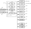
- the controller 221 as a control unit is configured as a computer including a CPU (Central Processing Unit) 221a, a RAM (Random Access Memory) 221b, a storage device 221c, and an I / O port 221d.
- the RAM 221b, the storage device 221c, and the I / O port 221d are configured to exchange data with the CPU 221a via the internal bus 221e.
- a touch panel, a mouse, a keyboard, an operation terminal, or the like may be connected to the controller 221 as the input / output device 225.
- a display or the like may be connected to the controller 221 as a display unit.
- the storage device 221c includes, for example, a flash memory, an HDD (Hard Disk Drive), a CD-ROM, and the like.
- a control program that controls the operation of the substrate processing apparatus 100, a process recipe that describes the procedure and conditions of the substrate processing, and the like are stored in a readable manner.
- the process recipe is a combination of functions so that a predetermined result can be obtained by causing the controller 221 to execute each procedure in a substrate processing step to be described later, and functions as a program.
- the process recipe, the control program, and the like are collectively referred to as simply a program.
- the RAM 221b is configured as a memory area (work area) in which a program, data, and the like read by the CPU 221a are temporarily stored.
- the I / O port 221d includes the above-described mass flow controllers 252a to 252c, valves 253a to 253c, 243a and 243b, gate valve 244, APC valve 242, vacuum pump 246, heater 217b, RF sensor 272, high frequency power supply 273, frequency matching unit 274, a susceptor elevating mechanism 268, an impedance variable mechanism 275, and the like.
- the CPU 221a is configured to read and execute a control program from the storage device 221c, and to read a process recipe from the storage device 221c in response to an operation command input from the input / output device 225 or the like. As shown in FIG. 1, the CPU 221a adjusts the opening degree of the APC valve 242, the opening / closing operation of the valve 243b, and the vacuum through the I / O port 221d and the signal line A in accordance with the contents of the read process recipe.
- the pump 246 is started / stopped, the susceptor lifting / lowering mechanism 268 is lifted / lowered through the signal line B, the power supply amount adjusting operation (temperature adjusting operation) to the heater 217b based on the temperature sensor through the signal line C, and the impedance by the impedance variable mechanism 275
- the value adjustment operation is performed by opening / closing the gate valve 244 through the signal line D, the operation of the RF sensor 272, the frequency matching unit 274, and the high frequency power supply 273 through the signal line E, and the mass flow controllers 252a to 252c through the signal line F.
- Flow adjustment operation and valves 253a to 253 c, 243a is controlled to open and close.
- the controller 221 is stored in an external storage device 226 (for example, a magnetic tape, a magnetic disk such as a flexible disk or a hard disk, an optical disk such as a CD or DVD, a magneto-optical disk such as an MO, or a semiconductor memory such as a USB memory or a memory card).
- the above-described program can be installed in a computer.
- the storage device 221c and the external storage device 226 are configured as computer-readable recording media. Hereinafter, these are collectively referred to simply as a recording medium.
- the term recording medium may include only the storage device 221c, only the external storage device 226, or both.
- the program may be provided to the computer by using communication means such as the Internet or a dedicated line without using the external storage device 226.
- the substrate processing process according to this embodiment is performed by the above-described processing apparatus 100 as one process of manufacturing a semiconductor device such as a flash memory.
- the operation of each part constituting the processing apparatus 100 is controlled by the controller 221.
- the wafer 200 to be processed in the substrate processing process according to the present embodiment has a silicon layer on the surface.
- a trench 301 having a concavo-convex portion (groove) with a high aspect ratio is formed in advance.
- the high aspect ratio (the ratio of the depth to the width of the trench) in the present embodiment means 10 times or more and at least 2 times or more.
- the trench 301 is formed, for example, by forming a mask layer 302 having a predetermined pattern on the wafer 200 and etching the surface of the wafer 200 to a predetermined depth.
- a nitriding process (nitride film formation or nitrogen dose) is performed on the silicon layer on the inner wall of the trench 301.
- the difference in the thickness of the nitride film between the upper part and the lower part (side wall part on the bottom side) of the side part 301b of the trench is reduced, or the nitride film on the bottom part 301a of the trench 301 and the nitride film on the side part 301b of the trench
- the processing apparatus is controlled so as to improve the step coverage which is the ratio of the thickness (that is, to reduce the ratio described on the left).
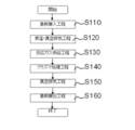
- the nitriding process will be described in detail with reference to the flowchart of FIG.
- the wafer 200 is loaded into the processing chamber 201. Specifically, the susceptor elevating mechanism 268 lowers the susceptor 217 to the transfer position of the wafer 200 and causes the wafer push-up pins 266 to pass through the through holes 217a of the susceptor 217. As a result, the wafer push-up pins 266 protrude from the surface of the susceptor 217 by a predetermined height.
- the gate valve 244 is opened, and the wafer 200 is loaded into the processing chamber 201 from a vacuum transfer chamber (not shown) adjacent to the processing chamber 201 using a transfer mechanism not shown in the drawing.
- the loaded wafer 200 is supported in a horizontal posture on the wafer push-up pins 266 protruding from the surface of the susceptor 217.
- the transfer mechanism is retracted out of the processing chamber 201, the gate valve 244 is closed, and the processing chamber 201 is sealed.
- the susceptor elevating mechanism 268 raises the susceptor 217 so as to be at a predetermined position between the lower end 203a of the resonance coil 212 and the upper end 245a of the loading / unloading port 245.
- the wafer 200 is supported on the upper surface of the susceptor 217.
- Particle generation amount can be adjusted.
- the substrate carry-in process S110 may be performed while purging the inside of the processing chamber 201 with an inert gas or the like.
- the temperature of the wafer 200 carried into the processing chamber 201 is increased.
- the heater 217b is preheated, and the wafer 200 loaded thereon is held on the susceptor 217 in which the heater 217b is embedded, so that the wafer 200 has a predetermined value of, for example, 100 ° C. or higher, and preferably 650 ° C. or higher and 900 ° C. or lower. Heat. If it is less than 100 ° C., the film forming rate may not be maintained. In order to form a good quality nitride film, it is desirable to perform nitriding at a high temperature of 650 ° C. or higher and 900 ° C. or lower.
- the temperature of the wafer 200 is heated to 700 ° C. Further, while the temperature of the wafer 200 is raised, the inside of the processing chamber 201 is evacuated by the vacuum pump 246 through the gas exhaust pipe 231, and the pressure in the processing chamber 201 is set to a predetermined value in the range of 1 Pa to 500 Pa. . For example, it is adjusted to 200 Pa. The vacuum pump 246 is operated until at least a substrate unloading step S160 described later is completed.
- Step S130 supply of N 2 gas as a reaction gas is started. Specifically, the supply of N 2 gas into the processing chamber 201 via the buffer chamber 237 is started while the valve 253a is opened and the flow rate is controlled by the mass flow controller 252a. At this time, the flow rate of the N 2 gas is set to a predetermined value within a range of, for example, 100 sccm to 1000 sccm, and more preferably 200 sccm. Further, the inside of the processing chamber 201 is evacuated by adjusting the opening of the APC 242 so that the pressure in the processing chamber 201 becomes a predetermined pressure of, for example, 1 Pa to 100 Pa, preferably 3 Pa to 10 Pa. In the present embodiment, adjustment is made so as to be particularly 5 Pa. In this way, while the processing chamber 201 is appropriately evacuated, the supply of N 2 gas is continued until the plasma processing step S140 described later is finished.
- High frequency power of 27.12 MHz is supplied at a power of, for example, 5.0 kW or less, preferably 3.5 kW or less, and more preferably 2.0 kW. In this embodiment, the power is supplied with 1.0 kW.
- a high-frequency electric field is formed in the plasma generation space 201a, and the doughnut-shaped induction plasma is excited by the electric field at a height corresponding to the electrical midpoint of the resonance coil 212 in the plasma generation space.
- the plasma N 2 gas is dissociated to generate nitrogen active species or reactive species such as radicals containing nitrogen element (N) (nitrogen radicals) and ions (nitrogen ions).
- the induction plasma excited at the electrical midpoint has almost no capacitive coupling with the processing chamber wall or the substrate mounting table, and a donut-shaped plasma having an extremely low electrical potential is generated in the plasma generation space 201a. Can be formed.
- the power supply control means attached to the high-frequency power supply 273 compensates for the shift of the resonance point in the resonance coil 212 due to fluctuations in plasma capacitive coupling and inductive coupling, and forms a standing wave more accurately.
- the plasma generation space can be formed more reliably in the plasma generation space with almost no capacitive coupling and extremely low electrical potential.
- nitrogen active species and reactive species for example, nitrogen radicals and ions that are not accelerated
- nitrogen active species and reactive species for example, nitrogen radicals and ions that are not accelerated
- the supplied radicals and ions react uniformly with the side walls 301a and 301b, and the silicon layer is modified into a silicon nitride film with good step coverage. Furthermore, since the occurrence of ion attack due to accelerated ions can be prevented, wafer damage due to ions can be suppressed.
- the acceleration of ions is prevented, there is no sputtering action on the peripheral wall of the plasma generation space 201a, and the peripheral wall of the plasma generation space 201a is not damaged.
- the lifetime of the apparatus can be improved, and in addition, it is possible to prevent the problem that member components such as the plasma generation space 201a are mixed into the plasma and contaminate the wafer.
- the power control means attached to the high frequency power supply 273 compensates the reflected wave power due to impedance mismatch generated in the resonance coil 212 on the high frequency power supply 273 side, and in order to compensate for the reduction in effective load power,
- the high frequency power at the initial level can always be reliably supplied, and the plasma can be stabilized. Therefore, the wafer held in the substrate processing space can be processed uniformly at a constant rate.
- Substrate unloading step S160 When the inside of the processing chamber 201 reaches a predetermined pressure, the susceptor 217 is lowered to the transfer position of the wafer 200 and the wafer 200 is supported on the wafer push-up pins 266. Then, the gate valve 244 is opened, and the wafer 200 is carried out of the processing chamber 201 using a transfer mechanism not shown in the drawing. At this time, the wafer 200 may be unloaded while purging the inside of the processing chamber 201 with an inert gas or the like. Thus, the substrate processing process according to this embodiment is completed.
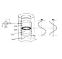
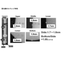
- FIG. 6 is a view showing an example in which a nitride film is formed in a trench having a silicon layer in the substrate processing step according to the embodiment of the present invention.
- the left figure (Overview) is an enlarged view of a trench having a depth d of 2.0 ⁇ m and a width W of 0.2 ⁇ m.
- the right figure is an enlarged view of the upper, middle, lower, container, and bottom of the trench when nitriding is performed in the embodiment of the present invention.
- the numerical value in the right figure indicates the film thickness of the film formed by nitriding.
- the nitride film formed according to the present invention has a film thickness of Upper of 1.8 nm, Middle of 1.8 nm, Lower of 1.7 nm, Corner of 1.8 nm, and Bottom of 1.8 nm. It can be seen that it is. This shows a substantially uniform step coverage characteristic. As a result, the characteristics of the semiconductor device are made uniform, and the variation in performance can be reduced.
- FIG. 7 shows the results of measuring the film thickness and in-plane uniformity values on the silicon substrate when nitriding is performed according to the present embodiment with an ellipsometer.
- the nitriding treatment according to the present embodiment 2.0 nm or more on the silicon substrate in the pressure region where the pressure in the processing chamber under the reaction gas (N 2 gas) atmosphere is in the range of 1 to 100 Pa. It can be confirmed that the nitride film can be formed with good uniformity. In the pressure region where the pressure in the processing chamber is less than 1 Pa, the film formation rate decreases rapidly, and a practical nitride film thickness (for example, 2.0 nm) cannot be realized.
- the in-plane uniformity of the nitride film is markedly deteriorated as the pressure increases, and better in-plane uniformity (uniformity of 10% or less) than the conventional technique. Can't keep up.
- a high film formation rate and good film thickness uniformity can be realized particularly in the range of 3 to 10 Pa.
- the pressure range of 3 to 10 Pa is particularly suitable when performing nitriding because it satisfies satisfactory in-plane uniformity and maximizes the deposition rate.
- the pressure in the processing chamber during nitriding is within a range in which the film formation rate and film thickness uniformity improve as the pressure decreases, more preferably 1 to Nitriding is performed in the range of 100 Pa, more preferably in the range of 3 to 10 Pa.
- N 2 nitrogen
- NH 3 ammonia
- NH 3 a mixed gas of N 2 gas and NH 3 gas
- a mixed gas obtained by adding a hydrogen (H 2 ) gas or a rare gas (Ar, He, Ne, etc.) as an inert gas to these gases may be used.
- H 2 gas hydrogen
- a rare gas Ar, He, Ne, etc.
- the total flow rate of the supplied gas and the pressure in the processing chamber 201 are the same as in the case of N 2 gas alone, and the flow rates of N 2 gas and H 2 gas are 1 : 1.
- the example in which the nitriding process is performed on the silicon layer on the inner wall of the trench 301 has been described.
- various films such as a gate insulating film and a metal film formed on the wafer 200 are processed.
- the silicon layer to be nitrided may be various types of silicon such as single crystal silicon, polysilicon, and amorphous silicon.
- other silicon-containing films, metal-containing films, and high-k films can be nitrided.
- a resonance coil configured as in the present embodiment, a plasma of a processing gas is generated under a low pressure condition, and the substrate surface is processed with the plasma, thereby forming a substrate surface having a high aspect ratio.
- a nitride film having good step coverage can be formed.
- the process pressure during plasma generation and substrate processing is in the range of 1 Pa to 100 Pa, more preferably 3 Pa to 10 Pa.
- a high film formation rate and good step coverage can be realized. This effect cannot be obtained simply by lowering the pressure in the processing chamber, and is remarkable when an ICP type substrate processing apparatus configured as in the present embodiment is used.
- the power control means such as a frequency matching unit attached to the high frequency power supply 273 compensates the reflected wave power due to impedance mismatch generated in the resonance coil 212 on the high frequency power supply 273 side, and compensates for a decrease in effective load power. Therefore, the initial level of high-frequency power can always be reliably supplied to the resonance coil 212, and the plasma can be stabilized. Therefore, the wafer held in the substrate processing space can be processed uniformly at a constant rate.
- the position of the resonance coil and the substrate can be adjusted by controlling the susceptor lifting mechanism so that the side and bottom of the groove are oxidized, so that good step coverage can be obtained. It becomes possible to control so that the film thickness of a side part and a bottom part becomes equivalent.
- the electric field formed in the processing chamber 201 is a high-frequency electric field having a frequency corresponding to the aspect ratio of the trench 301. Therefore, high-density plasma is obtained, and the arrival rate of the reactive species to the bottom 301a of the trench 301 is increased, and the processing efficiency inside the trench 301 is improved, so that finer and higher-speed processing is possible.
- the nitriding process using the N 2 gas has been described.
- the above-described processing apparatus 100 may be used to perform the oxidizing process using the O 2 gas that is an oxygen-containing gas.
- an oxidation process using O 2 gas will be described.
- an oxidation process is performed on the inner wall of the trench 301.
- the processing apparatus is controlled so as to improve the step coverage which is the ratio of the thickness of the oxide film between the bottom 301a of the trench 301 and the side 301b of the trench.
- the specific oxidation process is as shown in FIG. 4 as in the case of the nitriding process, and will be described in detail below with a particular focus on differences from the nitriding process.
- reaction gas supply step S130 After the temperature raising / evacuation step S120, in the reaction gas supply step, supply of O 2 gas as the reaction gas is started. Specifically, the supply of O 2 gas into the processing chamber 201 via the buffer chamber 237 is started while the valve 253a is opened and the flow rate is controlled by the mass flow controller 252a. At this time, the flow rate of the O 2 gas is set to a predetermined value within a range of 100 sccm to 1000 sccm, for example. Further, the opening of the processing chamber 201 is evacuated by adjusting the opening of the APC 242 so that the pressure in the processing chamber 201 is, for example, in the range of 1 Pa to 1000 Pa, preferably 150 Pa. In this manner, the supply of O 2 gas is continued until the plasma processing step S140 is completed while the processing chamber 201 is appropriately evacuated.
- a high-frequency electric field is formed in the plasma generation space 201a, and the doughnut-shaped induction plasma is excited by the electric field at a height corresponding to the electrical midpoint of the resonance coil 212 in the plasma generation space.
- the plasma O 2 gas is dissociated to generate oxygen active species or reactive species such as radicals containing oxygen (O) (oxygen radicals) and ions (oxygen ions).
- oxygen active species and reactive species for example, oxygen radicals and ions in an unaccelerated state
- oxygen active species and reactive species for example, oxygen radicals and ions in an unaccelerated state
- the supplied radicals and ions react uniformly with the side walls 301a and 301b, and the silicon layer is modified into a silicon oxide film with good step coverage.
- an oxidation process is performed using oxygen (O 2 ) gas.
- an oxidation process is performed by plasma-exciting a mixed gas of O 2 gas and hydrogen (H 2 ) gas. You can also.
- a mixed gas of O 2 gas and H 2 gas is activated by plasma, H, OH, and the like are generated. This OH oxidizes the surface of the silicon-containing layer to form an oxide film.
- this H has a stronger reducibility to the surface of the metal-containing layer than the reducibility to the surface of the silicon-containing layer.
- the surface of the silicon-containing layer can be selectively oxidized.
- a mixed gas to which H 2 gas is added is used, as an example, the total flow rate of the supplied gas and the pressure in the processing chamber 201 are the same as in the case of O 2 gas alone, and the flow rates of O 2 gas and H 2 gas are 50 sccm. : 950 sccm (5:95).
- oxygen-containing gas in addition to O 2 gas, nitrogen monoxide (NO) gas, nitrous oxide (N 2 O) gas, nitrogen dioxide (NO 2 ), or the like can be used.
- NO nitrogen monoxide
- N 2 O nitrous oxide
- NO 2 nitrogen dioxide
- a mixed gas obtained by adding a rare gas (Ar, He, Ne, etc.) as an inert gas to these gases can also be used. This rare gas contributes to stabilization of plasma discharge when plasma excitation is performed.
- an oxide film can be formed on the silicon substrate with good uniformity in the pressure range of 1 to 1000 Pa, preferably 150 Pa of reactive gas (O 2 gas).
- the floating electrode 603 already formed as shown in FIG. You can go.
- FIG. 8 will be specifically described.
- a plurality of columnar insulators 601 are formed on the surface of the wafer 200. Although two columnar insulators 601 are shown in FIG. 8, a large number of columnar insulators are adjacent to each other at a fine interval. They are not shown in the figure.
- a channel layer is formed in the columnar insulator 601.
- a gate insulating film 602 and a floating gate layer 603 are sequentially stacked in a direction perpendicular to the extending direction of the columnar insulator 601 in accordance with the channel layer.
- This stacked structure is called a flash memory stacked structure.
- the direction orthogonal to the extending direction of the columnar insulator 601 is also a direction parallel to the surface of the wafer 200.
- Another pattern is formed in the direction in which the stacked structure of the flash memory is extended.
- the stacked structure of the flash memory having the gate insulating film 602 and the floating gate layer 603 formed on the adjacent columnar insulator 601 is formed. Is formed. A narrow space is formed between the front end of the stacked structure of the flash memory and another pattern (here, between the floating gate layers 603 facing each other).
- a plurality of stacked structures of flash memories stacked in a direction orthogonal to the extending direction of the columnar insulator 601 are formed in parallel. Miniaturization is also performed between the stacked structures of flash memories.
- the front end 700 of the laminated structure for example, the front end 700 of the laminated structure, the side 701 existing in the supply direction of the inner gas on the side of the laminated structure, or the side opposite to the supply direction of the inner gas on the side of the laminated structure.
- the side surface 703 of the adjacent laminated structure 702 it is required to form a film uniformly because of the problem of device performance.
- the bottom 705, which is the bottom portion of the groove 704 between the laminated structures, is also required to be uniformly formed.
- oxygen active species and reactive species for example, oxygen radicals and unaccelerated ions
- oxygen radicals and unaccelerated ions are slowly and uniformly supplied into the trench 706. Therefore, the supplied radicals and ions are uniformly supplied to the stacked structure front end 700, the side surface 701, the side surface 702, the side surface 703, and the bottom surface 705. Therefore, the silicon layers at the front end 700, the side surface 701, the side surface 702, the side surface 703, and the bottom surface 705 of the laminated structure can be uniformly oxidized and modified into a silicon oxide film with high step coverage. In other words, a silicon oxide film with good step coverage can be formed. Furthermore, since ion attack due to acceleration can be prevented, wafer damage due to ions can be suppressed.
- the tip of the floating electrode 603 formed of polysilicon is uniformly oxidized, and the silicon oxide layer 604a in the ONO layer which is a charge storage layer is uniformly distributed on the substrate surface. Can be formed.
- the oxidation treatment in the present embodiment is applied to the silicon film already formed in one step of the manufacturing process of the three-dimensionally stacked flash memory has been described.
- the silicon layer on the surface of the three-dimensional pattern can be nitrided by applying the nitriding treatment in the first embodiment to the three-dimensional pattern.
- a substrate processing chamber having a plasma generation space in which the supplied nitrogen-containing gas is in a plasma state; a substrate processing space that communicates with the plasma generation space and on which a substrate is placed; and an outer periphery of the plasma generation space
- a length of an integral multiple of the wavelength of the high frequency power to which the electrical length (electrical length) of the coil and the impedance matching circuit is applied is configured by a coil and an impedance matching circuit connected to the coil.
- a substrate processing apparatus comprising: an inductive coupling structure; and a substrate mounting table configured to mount the substrate at a position below a lower end of the coil; and Placing the substrate; supplying the nitrogen-containing gas into the substrate processing chamber; and applying high-frequency power to the coil to generate the plasma.
- a method for manufacturing a semiconductor device or a substrate processing method wherein the pressure in the substrate processing chamber is set to a range of 1 Pa to 100 Pa.
- the substrate has a silicon-containing film on a surface thereof.
- the substrate is a substrate in which a structure (for example, a groove structure) having a high aspect ratio (10 times or more) is formed on the surface, and in the step of nitriding the surface of the substrate, At least the bottom and side surfaces of the structure having the high aspect ratio are nitrided.
- a structure for example, a groove structure having a high aspect ratio (10 times or more) is formed on the surface, and in the step of nitriding the surface of the substrate, At least the bottom and side surfaces of the structure having the high aspect ratio are nitrided.
- the substrate has a silicon-containing film, a metal-containing film, or a high-k film on a surface thereof.
- the process pressure is set in a range of 3 Pa to 10 Pa.
- the substrate mounting table includes a heater that heats the mounted substrate, and in the step of nitriding the substrate surface, the substrate is heated to 100 ° C. or higher (preferably 650 ° C.) by the heater. To 900 ° C. or lower).
- the nitrogen-containing gas is nitrogen (N 2 ) gas, ammonia (NH 3 ) gas, or a mixed gas of nitrogen gas and ammonia gas.
- Appendix 8 The method according to appendix 1, wherein after the step of placing the substrate on the substrate placing table, the substrate and the lower end of the coil have a predetermined distance in a range of 40 mm to 200 mm. A step of adjusting the position of the mounting table.
- a substrate processing chamber having a plasma generation space in which the supplied nitrogen-containing gas is plasma-excited; a substrate processing space that communicates with the plasma generation space and on which a substrate is placed; and an outer periphery of the plasma generation space
- a length of an integral multiple of the wavelength of the high frequency power to which the electrical length (electrical length) of the coil and the impedance matching circuit is applied is configured by a coil and an impedance matching circuit connected to the coil.
- An inductive coupling structure; and a substrate mounting table configured to mount the substrate at a position below the lower end of the coil.
- a substrate processing chamber having a plasma generation space in which a nitrogen-containing gas is plasma-excited, a substrate processing space that communicates with the plasma generation space and on which a substrate to be processed is placed, and is provided on the outer periphery of the plasma generation space
- a coil and an impedance matching circuit connected to the coil, and an electrical length (electrical length) of the coil and the impedance matching circuit is an integral multiple of the wavelength of the high-frequency power applied.
- a certain inductive coupling structure a substrate mounting table configured to mount the substrate at a position below a lower end of the coil; a gas supply unit that supplies a nitrogen-containing gas to the plasma generation space; and the substrate processing
- the high-frequency power is applied to the inductive coupling structure by controlling the exhaust unit for exhausting the room, the gas supply unit, and the exhaust unit, the substrate processing chamber
- the substrate processing apparatus having a configured controller to less 100Pa pressure.
- control unit configured to control the gas supply unit and the exhaust unit so that a pressure in the substrate processing chamber is in a range of 3 Pa to 10 Pa.
- Appendix 12 The substrate processing apparatus according to appendix 10, wherein the substrate mounting table includes a heater for heating the mounted substrate, and the control unit sets the substrate to be processed to 100 ° C. or higher (preferably 650 ° C. or higher).
- the heater is configured to be heated up to.
- Processing device 200 Wafer 201 ... Processing chamber 201a ... Plasma generation space 217 ... Susceptor 217b ... Heater 221 ... Controller 236 ... Gas supply head
Landscapes
- Engineering & Computer Science (AREA)
- Physics & Mathematics (AREA)
- Power Engineering (AREA)
- Microelectronics & Electronic Packaging (AREA)
- Plasma & Fusion (AREA)
- Condensed Matter Physics & Semiconductors (AREA)
- General Physics & Mathematics (AREA)
- Computer Hardware Design (AREA)
- Manufacturing & Machinery (AREA)
- Chemical & Material Sciences (AREA)
- Analytical Chemistry (AREA)
- Ceramic Engineering (AREA)
- Electromagnetism (AREA)
- Spectroscopy & Molecular Physics (AREA)
- Chemical Kinetics & Catalysis (AREA)
- Plasma Technology (AREA)
- Formation Of Insulating Films (AREA)
Abstract
Description
(1)基板処理装置の構成
本発明の第1実施形態に係る基板処理装置について、図1から図4を用いて以下に説明する。 <First embodiment of the present invention>
(1) Configuration of Substrate Processing Apparatus A substrate processing apparatus according to a first embodiment of the present invention will be described below with reference to FIGS.
処理装置100は、ウエハ200を誘導結合プラズマ(ICP :Inductively Coupled Plasma)方式のプラズマ処理を行う処理炉202を備えている。処理炉202には、処理室201を構成する処理容器203が設けられている。処理容器203は、第1の容器であるドーム型の上側容器210と、第2の容器である碗型の下側容器211とを備えている。上側容器210が下側容器211の上に被さることにより、処理室201が形成される。上側容器210は、例えば酸化アルミニウム(Al2O3)または石英(SiO2)等の非金属材料で形成されており、下側容器211は、例えばアルミニウム(Al)で形成されている。 (Processing room)
The
処理室201の底側中央には、ウエハ200を載置する基板載置部としてのサセプタ217が配置されている。サセプタ217は例えば窒化アルミニウム(AlN)、セラミックス、石英等の非金属材料から形成されており、ウエハ200上に形成される膜等の金属汚染を低減することができるように構成されている。 (Susceptor)
In the center of the bottom side of the
処理室201の上方、つまり上側容器210の上部には、ガス供給ヘッド236が設けられている。ガス供給ヘッド236は、キャップ状の蓋体233と、ガス導入口234と、バッファ室237と、開口238と、遮蔽プレート240と、ガス吹出口239とを備え、反応ガス(処理ガスともいう)を処理室201内へ供給できるように構成されている。バッファ室237は、ガス導入口234より導入される反応ガスを分散する分散空間としての機能を持つ。 (Gas supply part)
A
下側容器211の側壁には、処理室201内から反応ガスを排気するガス排気口235が設けられている。ガス排気口235には、ガス排気管231の上流端が接続されている。ガス排気管231には、上流側から順に圧力調整器(圧力調整部)としてのAPC(Auto Pressure Controller)242、開閉弁としてのバルブ243b、真空排気装置としての真空ポンプ246が設けられている。 (Exhaust part)
A
処理室201の外周部、すなわち上側容器210の側壁の外側には、処理室201を囲うように、第1の電極としての、螺旋状の共振コイル212が設けられている。共振コイル212には、RFセンサ272、高周波電源273と周波数整合器274が接続される。 (Plasma generator)
A
図3に示すように、制御部としてのコントローラ221は、CPU(Central Processing Unit)221a、RAM(Random Access Memory)221b、記憶装置221c、I/Oポート221dを備えたコンピュータとして構成されている。RAM221b、記憶装置221c、I/Oポート221dは、内部バス221eを介して、CPU221aとデータ交換可能なように構成されている。コントローラ221には、入出力装置225として、例えばタッチパネル、マウス、キーボード、操作端末等が接続されていてもよい。また、コントローラ221には、表示部として、例えばディスプレイ等が接続されていてもよい。 (Control part)
As shown in FIG. 3, the
次に、本実施形態に係る基板処理工程について、主に図4を用いて説明する。本実施形態に係る基板処理工程は、例えばフラッシュメモリ等の半導体デバイスの製造工程の一工程として、上述の処理装置100により実施される。なお以下の説明において、処理装置100を構成する各部の動作は、コントローラ221により制御される。 (2) Substrate Processing Step Next, the substrate processing step according to the present embodiment will be described mainly with reference to FIG. The substrate processing process according to this embodiment is performed by the above-described
まずは、上記のウエハ200を処理室201内に搬入する。具体的には、サセプタ昇降機構268がウエハ200の搬送位置までサセプタ217を下降させて、サセプタ217の貫通孔217aにウエハ突上げピン266を貫通させる。その結果、ウエハ突き上げピン266が、サセプタ217表面よりも所定の高さ分だけ突出した状態となる。 (Substrate carrying-in process S110)
First, the
続いて、処理室201内に搬入されたウエハ200の昇温を行う。ヒータ217bは予め加熱されており、ヒータ217bが埋め込まれたサセプタ217上に、搬入されたウエハ200を保持することで、例えば100℃以上、望ましくは650℃以上900℃以下の所定値にウエハ200を加熱する。100℃未満では成膜レートが維持できない可能性がある。また、良質な窒化膜を形成するためには、650℃以上900℃以下の高温で窒化処理を行うことが望ましい。ここでは、ウエハ200の温度が700℃となるよう加熱する。また、ウエハ200の昇温を行う間、真空ポンプ246によりガス排気管231を介して処理室201内を真空排気し、処理室201内の圧力を1Pa以上500Pa以下の範囲内の所定値とする。例えば200Paに調整される。真空ポンプ246は、少なくとも後述の基板搬出工程S160が終了するまで作動させておく。 (Temperature raising / evacuation process S120)
Subsequently, the temperature of the
次に、反応ガスとしてのN2ガスの供給を開始する。具体的には、バルブ253aを開け、マスフローコントローラ252aにて流量制御しながら、バッファ室237を介して処理室201内へのN2ガスの供給を開始する。このとき、N2ガスの流量を、例えば100sccm以上1000sccm以下の範囲内の所定値、より好ましくは200sccmとする。また、処理室201内の圧力が、例えば1Pa以上100Pa以下の範囲内、好ましくは3Pa以上10Pa以下の所定圧力となるように、APC242の開度を調整して処理室201内を排気する。本実施形態では特に5Paとなるように調整する。このように、処理室201内を適度に排気しつつ、後述のプラズマ処理工程S140の終了時までN2ガスの供給を継続する。 (Reactive gas supply step S130)
Next, supply of N 2 gas as a reaction gas is started. Specifically, the supply of N 2 gas into the
処理室201内の圧力が安定したら、共振コイル212に対して、高周波電源273から高周波電力の印加を開始する。本実施形態では、27.12MHzの高周波電力を、例えば5.0kW以下、好ましくは3.5kW以下、より好ましくは2.0kWの電力で供給する。本実施形態では、特に1.0kWの電力で供給する。 (Plasma treatment step S140)
When the pressure in the
所定の処理時間が経過してN2ガスの供給を停止したら、ガス排気管231を用いて処理室201内を真空排気する。これにより、処理室201内のN2ガスや、N2ガスが反応した排ガス等を処理室201外へと排気する。その後、APC242の開度を調整し、処理室201内の圧力を処理室201に隣接する真空搬送室(ウエハ200の搬出先。図示せず)と同じ圧力(例えば100Pa)に調整する。 (Evacuation step S150)
When the supply of N 2 gas is stopped after a predetermined processing time has elapsed, the inside of the
処理室201内が所定の圧力となったら、サセプタ217をウエハ200の搬送位置まで下降させ、ウエハ突上げピン266上にウエハ200を支持させる。そして、ゲートバルブ244を開き、図中省略の搬送機構を用いてウエハ200を処理室201外へ搬出する。このとき、処理室201内を不活性ガス等でパージしながらウエハ200の搬出を行ってもよい。以上により、本実施形態に係る基板処理工程を終了する。 (Substrate unloading step S160)
When the inside of the
本実施形態によれば、以下に示す1つまたは複数の効果を奏する。 (3) Effects according to the present embodiment According to the present embodiment, the following one or more effects are achieved.
本実施形態においては、トレンチ301の内壁に対して酸化処理を行う。その際、トレンチ301の底部301aとトレンチの側部301bの酸化膜の厚さの比率であるステップカバレッジを良好にするよう、処理装置を制御するものである。なお、具体的な当該酸化処理の工程は、窒化処理の場合と同様、図4に示す通りであり、以下では、窒化処理の場合と特に異なる部分を中心に詳述する。 <Second Embodiment>
In the present embodiment, an oxidation process is performed on the inner wall of the
昇温・真空排気工程S120の後、反応ガス供給工程では、反応ガスとしてのO2ガスの供給を開始する。具体的には、バルブ253aを開け、マスフローコントローラ252aにて流量制御しながら、バッファ室237を介して処理室201内へのO2ガスの供給を開始する。このとき、O2ガスの流量を、例えば100sccm以上1000sccm以下の範囲内の所定値とする。また、処理室201内の圧力が、例えば1Pa以上1000Pa以下の範囲内、好ましくは150Paとなるように、APC242の開度を調整して処理室201内を排気する。このように、処理室201内を適度に排気しつつ、プラズマ処理工程S140の終了時までO2ガスの供給を継続する。 (Reactive gas supply step S130)
After the temperature raising / evacuation step S120, in the reaction gas supply step, supply of O 2 gas as the reaction gas is started. Specifically, the supply of O 2 gas into the
処理室201内の圧力が安定したら、共振コイル212に対して、高周波電源273から高周波電力の印加を開始する。 (Plasma treatment step S140)
When the pressure in the
供給された窒素含有ガスがプラズマ状態となるプラズマ生成空間と、前記プラズマ生成空間に連通し基板処理時に基板が載置される基板処理空間と、を有する基板処理室と、前記プラズマ生成空間の外周に設けられ、コイルと前記コイルに接続されるインピーダンスマッチング回路により構成され、前記コイルと前記インピーダンスマッチング回路を合わせた電気長(電気的長さ)が印加される高周波電力の波長の整数倍の長さである誘導結合構造と、前記基板を前記コイルの下端より下の位置に載置するように構成された基板載置台と、を備えた基板処理装置を準備する工程と、前記基板載置台に前記基板を載置する工程と、前記基板処理室内に前記窒素含有ガスを供給する工程と、前記コイルに高周波電力を印加して、前記プラズマ生成空間において前記窒素含有ガスのプラズマ励起を開始する工程と、前記プラズマ励起によって発生した窒素元素を含む活性種(反応種)により前記基板の表面を窒化する工程と、を有し、前記基板表面を窒化する工程では、基板処理室内の圧力を1Pa以上100Pa以下の範囲とする、半導体装置の製造方法又は基板処理方法。 [Appendix 1]
A substrate processing chamber having a plasma generation space in which the supplied nitrogen-containing gas is in a plasma state; a substrate processing space that communicates with the plasma generation space and on which a substrate is placed; and an outer periphery of the plasma generation space A length of an integral multiple of the wavelength of the high frequency power to which the electrical length (electrical length) of the coil and the impedance matching circuit is applied is configured by a coil and an impedance matching circuit connected to the coil. A substrate processing apparatus comprising: an inductive coupling structure; and a substrate mounting table configured to mount the substrate at a position below a lower end of the coil; and Placing the substrate; supplying the nitrogen-containing gas into the substrate processing chamber; and applying high-frequency power to the coil to generate the plasma. A step of initiating plasma excitation of the nitrogen-containing gas, and a step of nitriding the surface of the substrate with an active species (reactive species) containing nitrogen element generated by the plasma excitation. In the nitriding step, a method for manufacturing a semiconductor device or a substrate processing method, wherein the pressure in the substrate processing chamber is set to a range of 1 Pa to 100 Pa.
付記1に記載の方法において、前記基板は、表面にシリコン含有膜を有する。 [Appendix 2]
In the method according to
付記1又は2に記載の方法において、前記基板は、表面に高アスペクト比(10倍以上)を有する構造(例えば溝構造)が形成された基板であり、前記基板の表面を窒化する工程では、前記高アスペクト比を有する構造の底面及び側面を少なくとも窒化する。 [Appendix 3]
In the method according to
付記1乃至3のいずれかに記載の方法において、前記基板は、表面にシリコン含有膜、金属含有膜、High-k膜のいずれかを有する。 [Appendix 4]
In the method according to any one of
付記1に記載の方法において、前記基板表面を窒化する工程では、前記プロセス圧力を3Pa以上10Pa以下の範囲とする。 [Appendix 5]
In the method according to
付記1に記載の方法において、前記基板載置台は、載置された前記基板を加熱するヒータを備え、前記基板表面を窒化する工程では、前記基板は前記ヒータにより100℃以上(望ましくは650℃以上900℃以下)まで加熱される。 [Appendix 6]
In the method according to
付記1に記載の方法において、前記窒素含有ガスは、窒素(N2)ガス、アンモニア(NH3)ガス、又は窒素ガスとアンモニアガスの混合ガスである。 [Appendix 7]
In the method according to
付記1に記載の方法において、前記基板載置台に前記基板を載置する工程の後、前記基板と前記コイルの下端との距離を40mm以上200mm以下の範囲の所定の距離となるように前記基板載置台の位置を調整する工程を有する。 [Appendix 8]
The method according to
供給された窒素含有ガスがプラズマ励起されるプラズマ生成空間と、前記プラズマ生成空間に連通し基板処理時に基板が載置される基板処理空間と、を有する基板処理室と、前記プラズマ生成空間の外周に設けられ、コイルと前記コイルに接続されるインピーダンスマッチング回路により構成され、前記コイルと前記インピーダンスマッチング回路を合わせた電気長(電気的長さ)が印加される高周波電力の波長の整数倍の長さである誘導結合構造と、前記基板を前記コイルの下端より下の位置に載置するように構成された基板載置台と、を備えた基板処理装置において、前記基板載置台に前記基板を載置する手順と、前記基板処理室内に前記窒素含有ガスを供給する手順と、前記コイルに高周波電力を印加して、前記プラズマ生成空間において前記窒素含有ガスのプラズマ励起を開始する手順と、前記プラズマ励起によって発生した窒素元素を含む活性種(反応種)により前記基板の表面を窒化する手順と、をコンピュータに実行させ、前記基板表面を窒化する手順では基板処理室内の圧力を1Pa以上100Pa以下の範囲とするプログラム、又は該プログラムを記録したコンピュータが読み取り可能な記録媒体。 [Appendix 9]
A substrate processing chamber having a plasma generation space in which the supplied nitrogen-containing gas is plasma-excited; a substrate processing space that communicates with the plasma generation space and on which a substrate is placed; and an outer periphery of the plasma generation space A length of an integral multiple of the wavelength of the high frequency power to which the electrical length (electrical length) of the coil and the impedance matching circuit is applied is configured by a coil and an impedance matching circuit connected to the coil. An inductive coupling structure; and a substrate mounting table configured to mount the substrate at a position below the lower end of the coil. Placing the nitrogen-containing gas into the substrate processing chamber, applying high frequency power to the coil, and A step of starting a plasma excitation of the nitrogen-containing gas and a step of nitriding the surface of the substrate with an active species (reactive species) containing a nitrogen element generated by the plasma excitation, In the procedure for nitriding, a program for setting the pressure in the substrate processing chamber to a range of 1 Pa or more and 100 Pa or less, or a computer-readable recording medium on which the program is recorded.
窒素含有ガスがプラズマ励起されるプラズマ生成空間と、前記プラズマ生成空間に連通し、処理される基板が載置される基板処理空間と、を有する基板処理室と、前記プラズマ生成空間の外周に設けられ、コイルと前記コイルに接続されるインピーダンスマッチング回路により構成され、前記コイルと前記インピーダンスマッチング回路を合わせた電気長(電気的長さ)が印加される高周波電力の波長の整数倍の長さである誘導結合構造と、前記基板を前記コイルの下端より下の位置に載置するように構成された基板載置台と、前記プラズマ生成空間に窒素含有ガスを供給するガス供給部と、前記基板処理室内を排気する排気部と、前記ガス供給部と前記排気部を制御して、前記誘導結合構造に高周波電力が印加される際、前記基板処理室内の圧力を100Pa以下とするよう構成される制御部と、を有する基板処理装置。 [Appendix 10]
A substrate processing chamber having a plasma generation space in which a nitrogen-containing gas is plasma-excited, a substrate processing space that communicates with the plasma generation space and on which a substrate to be processed is placed, and is provided on the outer periphery of the plasma generation space A coil and an impedance matching circuit connected to the coil, and an electrical length (electrical length) of the coil and the impedance matching circuit is an integral multiple of the wavelength of the high-frequency power applied. A certain inductive coupling structure; a substrate mounting table configured to mount the substrate at a position below a lower end of the coil; a gas supply unit that supplies a nitrogen-containing gas to the plasma generation space; and the substrate processing When the high-frequency power is applied to the inductive coupling structure by controlling the exhaust unit for exhausting the room, the gas supply unit, and the exhaust unit, the substrate processing chamber A substrate processing apparatus having a configured controller to less 100Pa pressure.
付記10に記載の基板処理装置において、前記制御部は、前記基板処理室内の圧力を3Pa以上10Pa以下の範囲とするよう、前記ガス供給部と前記排気部を制御するように構成される。 [Appendix 11]
The substrate processing apparatus according to
付記10に記載の基板処理装置において、前記基板載置台は、載置された前記基板を加熱するヒータを備え、前記制御部は、前記処理される基板を100℃以上(望ましくは650℃以上)まで加熱するよう、前記ヒータを制御するよう構成される。 [Appendix 12]
The substrate processing apparatus according to
Claims (11)
- 供給された窒素含有ガスがプラズマ励起されるプラズマ生成空間と、前記プラズマ生成空間に連通し基板処理時に基板が載置される基板処理空間と、を有する基板処理室と、前記プラズマ生成空間の外周に設けられ、コイルと前記コイルに接続されるインピーダンスマッチング回路により構成され、前記コイルと前記インピーダンスマッチング回路を合わせた電気長が印加される高周波電力の波長の整数倍の長さである誘導結合構造と、前記基板を前記コイルの下端より下の位置に載置するように構成された基板載置台と、を備えた基板処理装置を準備する工程と、
前記基板載置台に前記基板を載置する工程と、
前記基板処理室内に前記窒素含有ガスを供給する工程と、
前記コイルに高周波電力を印加して、前記プラズマ生成空間において前記窒素含有ガスのプラズマ励起を開始する工程と、
前記プラズマ励起によって発生した窒素元素を含む活性種により前記基板の表面を窒化する工程と、を有し、
前記基板表面を窒化する工程では、基板処理室内の圧力を1Pa以上100Pa以下の範囲とする、半導体装置の製造方法。 A substrate processing chamber having a plasma generation space in which the supplied nitrogen-containing gas is plasma-excited; a substrate processing space that communicates with the plasma generation space and on which a substrate is placed; and an outer periphery of the plasma generation space An inductive coupling structure comprising a coil and an impedance matching circuit connected to the coil, wherein the combined electrical length of the coil and the impedance matching circuit is an integral multiple of the wavelength of the high-frequency power applied Preparing a substrate processing apparatus comprising: a substrate mounting table configured to mount the substrate at a position below the lower end of the coil; and
Mounting the substrate on the substrate mounting table;
Supplying the nitrogen-containing gas into the substrate processing chamber;
Applying high frequency power to the coil to initiate plasma excitation of the nitrogen-containing gas in the plasma generation space;
Nitriding the surface of the substrate with active species containing nitrogen element generated by the plasma excitation,
A method of manufacturing a semiconductor device, wherein, in the step of nitriding the substrate surface, the pressure in the substrate processing chamber is set to a range of 1 Pa to 100 Pa. - 請求項1に記載の半導体装置の製造方法であって、
前記基板は、表面に10倍以上のアスペクト比を有する構造が形成された基板であり、
前記基板の表面を窒化する工程では、前記構造の底面及び側面を少なくとも窒化する。 A method of manufacturing a semiconductor device according to claim 1,
The substrate is a substrate in which a structure having an aspect ratio of 10 times or more is formed on the surface,
In the step of nitriding the surface of the substrate, at least the bottom and side surfaces of the structure are nitrided. - 請求項2に記載の半導体装置の製造方法であって、
前記基板は、表面にシリコン含有膜、金属含有膜及びHigh-k膜の少なくともいずれかを有する。 A method of manufacturing a semiconductor device according to claim 2,
The substrate has at least one of a silicon-containing film, a metal-containing film, and a high-k film on the surface. - 請求項1に記載の半導体装置の製造方法であって、
前記基板表面を窒化する工程では、前記基板処理室内の圧力を3Pa以上10Pa以下の範囲とする。 A method of manufacturing a semiconductor device according to claim 1,
In the step of nitriding the substrate surface, the pressure in the substrate processing chamber is set to a range of 3 Pa to 10 Pa. - 請求項1に記載の半導体装置の製造方法であって、
前記基板載置台は、載置された前記基板を加熱するヒータを備え、前記基板表面を窒化する工程では、前記基板は前記ヒータにより650℃以上900℃以下の範囲の温度まで加熱される。 A method of manufacturing a semiconductor device according to claim 1,
The substrate mounting table includes a heater for heating the mounted substrate. In the step of nitriding the substrate surface, the substrate is heated to a temperature in the range of 650 ° C. to 900 ° C. by the heater. - 請求項1に記載の半導体装置の製造方法であって、
前記窒素含有ガスは、窒素ガス、アンモニアガス、又は窒素ガスとアンモニアガスの混合ガスである。 A method of manufacturing a semiconductor device according to claim 1,
The nitrogen-containing gas is nitrogen gas, ammonia gas, or a mixed gas of nitrogen gas and ammonia gas. - 請求項1に記載の半導体装置の製造方法であって、
前記基板載置台に前記基板を載置する工程の後、前記基板と前記コイルの下端との距離を40mm以上200mm以下の範囲の所定の距離となるように前記基板載置台の位置を調整する工程を有する。 A method of manufacturing a semiconductor device according to claim 1,
After the step of placing the substrate on the substrate platform, the step of adjusting the position of the substrate platform so that the distance between the substrate and the lower end of the coil is a predetermined distance in the range of 40 mm to 200 mm. Have - 供給された窒素含有ガスがプラズマ励起されるプラズマ生成空間と、前記プラズマ生成空間に連通し基板処理時に基板が載置される基板処理空間と、を有する基板処理室と、前記プラズマ生成空間の外周に設けられ、コイルと前記コイルに接続されるインピーダンスマッチング回路により構成され、前記コイルと前記インピーダンスマッチング回路を合わせた電気長が印加される高周波電力の波長の整数倍の長さである誘導結合構造と、前記基板を前記コイルの下端より下の位置に載置するように構成された基板載置台と、を備えた基板処理装置において、
前記基板載置台に前記基板を載置する手順と、
前記基板処理室内に前記窒素含有ガスを供給する手順と、
前記コイルに高周波電力を印加して、前記プラズマ生成空間において前記窒素含有ガスのプラズマ励起を開始する手順と、
前記プラズマ励起によって発生した窒素元素を含む活性種により前記基板の表面を窒化する手順と、をコンピュータに実行させ、
前記基板表面を窒化する手順では基板処理室内の圧力を1Pa以上100Pa以下の範囲とするプログラムを記録したコンピュータが読み取り可能な記録媒体。 A substrate processing chamber having a plasma generation space in which the supplied nitrogen-containing gas is plasma-excited; a substrate processing space that communicates with the plasma generation space and on which a substrate is placed; and an outer periphery of the plasma generation space An inductive coupling structure comprising a coil and an impedance matching circuit connected to the coil, wherein the combined electrical length of the coil and the impedance matching circuit is an integral multiple of the wavelength of the high-frequency power applied And a substrate mounting table configured to place the substrate at a position below the lower end of the coil.
A procedure for mounting the substrate on the substrate mounting table;
Supplying the nitrogen-containing gas into the substrate processing chamber;
Applying high frequency power to the coil to start plasma excitation of the nitrogen-containing gas in the plasma generation space;
Causing the computer to execute a procedure of nitriding the surface of the substrate with an active species containing nitrogen element generated by the plasma excitation,
A computer-readable recording medium that records a program for setting the pressure in the substrate processing chamber to a range of 1 Pa to 100 Pa in the procedure of nitriding the substrate surface. - 窒素含有ガスがプラズマ励起されるプラズマ生成空間と、前記プラズマ生成空間に連通し、処理される基板が載置される基板処理空間と、を有する基板処理室と、
前記プラズマ生成空間の外周に設けられ、コイルと前記コイルに接続されるインピーダンスマッチング回路により構成され、前記コイルと前記インピーダンスマッチング回路を合わせた電気長が印加される高周波電力の波長の整数倍の長さである誘導結合構造と、
前記基板を前記コイルの下端より下の位置に載置するように構成された基板載置台と、
前記プラズマ生成空間に前記窒素含有ガスを供給するガス供給部と、
前記基板処理室内を排気する排気部と、
前記ガス供給部と前記排気部を制御して、前記誘導結合構造に高周波電力が印加される際、前記基板処理室内の圧力を1Pa以上100Pa以下の範囲とするよう構成される制御部と、を有する基板処理装置。 A substrate processing chamber having a plasma generation space in which a nitrogen-containing gas is plasma-excited, and a substrate processing space in communication with the plasma generation space in which a substrate to be processed is placed;
A length that is an integer multiple of the wavelength of the high-frequency power that is provided on the outer periphery of the plasma generation space, is configured by a coil and an impedance matching circuit that is connected to the coil, and the combined electrical length of the coil and the impedance matching circuit is applied. An inductive coupling structure,
A substrate mounting table configured to mount the substrate at a position below the lower end of the coil;
A gas supply unit for supplying the nitrogen-containing gas to the plasma generation space;
An exhaust section for exhausting the substrate processing chamber;
A control unit configured to control the gas supply unit and the exhaust unit so that when high frequency power is applied to the inductive coupling structure, the pressure in the substrate processing chamber is in a range of 1 Pa to 100 Pa. A substrate processing apparatus. - 請求項9に記載の基板処理装置であって、
前記制御部は、前記基板処理室内の圧力を3Pa以上10Pa以下の範囲とするよう前記ガス供給部と前記排気部を制御するように構成される。 The substrate processing apparatus according to claim 9, comprising:
The control unit is configured to control the gas supply unit and the exhaust unit so that a pressure in the substrate processing chamber is in a range of 3 Pa to 10 Pa. - 請求項9に記載の基板処理装置であって、
前記基板載置台は、載置された前記基板を加熱するヒータを備え、前記制御部は、前記処理される基板を650℃以上900℃以下の範囲の温度まで加熱するよう、前記ヒータを制御するよう構成される。 The substrate processing apparatus according to claim 9, comprising:
The substrate mounting table includes a heater for heating the mounted substrate, and the control unit controls the heater so as to heat the substrate to be processed to a temperature in the range of 650 ° C. to 900 ° C. It is configured as follows.
Priority Applications (3)
| Application Number | Priority Date | Filing Date | Title |
|---|---|---|---|
| JP2016566157A JP6281964B2 (en) | 2014-12-25 | 2015-12-16 | Semiconductor device manufacturing method, program, and substrate processing apparatus |
| KR1020177017370A KR101965992B1 (en) | 2014-12-25 | 2015-12-16 | Semiconductor device manufacturing method, recording medium, and substrate processing device |
| US15/630,472 US10453676B2 (en) | 2014-12-25 | 2017-06-22 | Semiconductor device manufacturing method and recording medium |
Applications Claiming Priority (2)
| Application Number | Priority Date | Filing Date | Title |
|---|---|---|---|
| JP2014-262686 | 2014-12-25 | ||
| JP2014262686 | 2014-12-25 |
Related Child Applications (1)
| Application Number | Title | Priority Date | Filing Date |
|---|---|---|---|
| US15/630,472 Continuation US10453676B2 (en) | 2014-12-25 | 2017-06-22 | Semiconductor device manufacturing method and recording medium |
Publications (1)
| Publication Number | Publication Date |
|---|---|
| WO2016104292A1 true WO2016104292A1 (en) | 2016-06-30 |
Family
ID=56150315
Family Applications (1)
| Application Number | Title | Priority Date | Filing Date |
|---|---|---|---|
| PCT/JP2015/085247 WO2016104292A1 (en) | 2014-12-25 | 2015-12-16 | Semiconductor device manufacturing method, recording medium, and substrate processing device |
Country Status (4)
| Country | Link |
|---|---|
| US (1) | US10453676B2 (en) |
| JP (1) | JP6281964B2 (en) |
| KR (1) | KR101965992B1 (en) |
| WO (1) | WO2016104292A1 (en) |
Cited By (1)
| Publication number | Priority date | Publication date | Assignee | Title |
|---|---|---|---|---|
| JP2020517097A (en) * | 2017-04-07 | 2020-06-11 | アプライド マテリアルズ インコーポレイテッドApplied Materials,Incorporated | Surface modification to improve amorphous silicon gap filling |
Families Citing this family (1)
| Publication number | Priority date | Publication date | Assignee | Title |
|---|---|---|---|---|
| KR102253808B1 (en) * | 2019-01-18 | 2021-05-20 | 주식회사 유진테크 | Apparatus for processing substrate |
Citations (9)
| Publication number | Priority date | Publication date | Assignee | Title |
|---|---|---|---|---|
| US5888414A (en) * | 1991-06-27 | 1999-03-30 | Applied Materials, Inc. | Plasma reactor and processes using RF inductive coupling and scavenger temperature control |
| JPH11162697A (en) * | 1997-11-28 | 1999-06-18 | Mc Electronics Kk | Spiral resonance device for plasma generation |
| JP2004186402A (en) * | 2002-06-19 | 2004-07-02 | Mitsubishi Heavy Ind Ltd | Plasma processing apparatus and method therefor |
| JP2009224755A (en) * | 2008-02-19 | 2009-10-01 | Hitachi Kokusai Electric Inc | Method of manufacturing semiconductor device, and substrate processing apparatus |
| JP2009272547A (en) * | 2008-05-09 | 2009-11-19 | Tokyo Electron Ltd | Method of manufacturing semiconductor device |
| JP2011165743A (en) * | 2010-02-05 | 2011-08-25 | Hitachi Kokusai Electric Inc | Method of manufacturing semiconductor-device |
| JP2012522399A (en) * | 2009-03-31 | 2012-09-20 | アプライド マテリアルズ インコーポレイテッド | Method of selective nitrogenation |
| JP2014075579A (en) * | 2012-09-12 | 2014-04-24 | Hitachi Kokusai Electric Inc | Substrate processing apparatus and manufacturing method of semiconductor device |
| US20140273517A1 (en) * | 2013-03-15 | 2014-09-18 | Applied Materials, Inc. | Nh3 containing plasma nitridation of a layer of a three dimensional structure on a substrate |
Family Cites Families (13)
| Publication number | Priority date | Publication date | Assignee | Title |
|---|---|---|---|---|
| US6238528B1 (en) * | 1998-10-13 | 2001-05-29 | Applied Materials, Inc. | Plasma density modulator for improved plasma density uniformity and thickness uniformity in an ionized metal plasma source |
| US20030072884A1 (en) * | 2001-10-15 | 2003-04-17 | Applied Materials, Inc. | Method of titanium and titanium nitride layer deposition |
| WO2006049130A1 (en) * | 2004-11-05 | 2006-05-11 | Hitachi Kokusai Electric Inc. | Method for manufacturing semiconductor device |
| US7688272B2 (en) * | 2005-05-30 | 2010-03-30 | Semiconductor Energy Laboratory Co., Ltd. | Semiconductor device |
| TWM303190U (en) * | 2006-06-29 | 2006-12-21 | Thn Shong Ind Co Ltd | Rubbish bin with bag-clamping apparatus |
| WO2008008098A2 (en) * | 2006-07-07 | 2008-01-17 | Silica Tech, Llc | Plasma deposition apparatus and method for making polycrystalline silicon |
| US8285646B2 (en) * | 2007-03-19 | 2012-10-09 | Igt | Centralized licensing services |
| US20090233430A1 (en) | 2008-02-19 | 2009-09-17 | Hitachi-Kokusai Electric In. | Semiconductor device manufacturing method, semiconductor device manufacturing apparatus, and semiconductor device manufacturing system |
| JP2011164743A (en) | 2010-02-05 | 2011-08-25 | Seiko Epson Corp | Storage device and storage method |
| US8485527B2 (en) * | 2011-07-29 | 2013-07-16 | Savant Shuffler LLC | Card shuffler |
| JP5933394B2 (en) * | 2011-09-22 | 2016-06-08 | 株式会社日立国際電気 | Substrate processing apparatus, semiconductor device manufacturing method, and program |
| JP2013182966A (en) * | 2012-03-01 | 2013-09-12 | Hitachi High-Technologies Corp | Plasma processing apparatus and plasma processing method |
| US9012336B2 (en) * | 2013-04-08 | 2015-04-21 | Applied Materials, Inc. | Method for conformal treatment of dielectric films using inductively coupled plasma |
-
2015
- 2015-12-16 WO PCT/JP2015/085247 patent/WO2016104292A1/en active Application Filing
- 2015-12-16 KR KR1020177017370A patent/KR101965992B1/en active IP Right Grant
- 2015-12-16 JP JP2016566157A patent/JP6281964B2/en active Active
-
2017
- 2017-06-22 US US15/630,472 patent/US10453676B2/en active Active
Patent Citations (9)
| Publication number | Priority date | Publication date | Assignee | Title |
|---|---|---|---|---|
| US5888414A (en) * | 1991-06-27 | 1999-03-30 | Applied Materials, Inc. | Plasma reactor and processes using RF inductive coupling and scavenger temperature control |
| JPH11162697A (en) * | 1997-11-28 | 1999-06-18 | Mc Electronics Kk | Spiral resonance device for plasma generation |
| JP2004186402A (en) * | 2002-06-19 | 2004-07-02 | Mitsubishi Heavy Ind Ltd | Plasma processing apparatus and method therefor |
| JP2009224755A (en) * | 2008-02-19 | 2009-10-01 | Hitachi Kokusai Electric Inc | Method of manufacturing semiconductor device, and substrate processing apparatus |
| JP2009272547A (en) * | 2008-05-09 | 2009-11-19 | Tokyo Electron Ltd | Method of manufacturing semiconductor device |
| JP2012522399A (en) * | 2009-03-31 | 2012-09-20 | アプライド マテリアルズ インコーポレイテッド | Method of selective nitrogenation |
| JP2011165743A (en) * | 2010-02-05 | 2011-08-25 | Hitachi Kokusai Electric Inc | Method of manufacturing semiconductor-device |
| JP2014075579A (en) * | 2012-09-12 | 2014-04-24 | Hitachi Kokusai Electric Inc | Substrate processing apparatus and manufacturing method of semiconductor device |
| US20140273517A1 (en) * | 2013-03-15 | 2014-09-18 | Applied Materials, Inc. | Nh3 containing plasma nitridation of a layer of a three dimensional structure on a substrate |
Cited By (2)
| Publication number | Priority date | Publication date | Assignee | Title |
|---|---|---|---|---|
| JP2020517097A (en) * | 2017-04-07 | 2020-06-11 | アプライド マテリアルズ インコーポレイテッドApplied Materials,Incorporated | Surface modification to improve amorphous silicon gap filling |
| JP7101191B2 (en) | 2017-04-07 | 2022-07-14 | アプライド マテリアルズ インコーポレイテッド | Surface modification to improve amorphous silicon gap filling |
Also Published As
| Publication number | Publication date |
|---|---|
| KR101965992B1 (en) | 2019-04-04 |
| KR20170086639A (en) | 2017-07-26 |
| JP6281964B2 (en) | 2018-02-21 |
| US10453676B2 (en) | 2019-10-22 |
| US20170287707A1 (en) | 2017-10-05 |
| JPWO2016104292A1 (en) | 2017-11-02 |
Similar Documents
| Publication | Publication Date | Title |
|---|---|---|
| JP6257071B2 (en) | Substrate processing apparatus and semiconductor device manufacturing method | |
| JP6649473B2 (en) | Substrate processing apparatus, semiconductor device manufacturing method and program | |
| JP6285052B2 (en) | Semiconductor device manufacturing method, program, and substrate processing apparatus | |
| JP6748779B2 (en) | Semiconductor device manufacturing method, program, and substrate processing apparatus | |
| CN111096082B (en) | Substrate processing apparatus, method of manufacturing semiconductor device, and recording medium | |
| WO2018179352A1 (en) | Method for manufacturing semiconductor device, and recording medium | |
| JP6281964B2 (en) | Semiconductor device manufacturing method, program, and substrate processing apparatus | |
| JP6436886B2 (en) | Semiconductor device manufacturing method and program | |
| KR102465993B1 (en) | Substrate processing apparatus, method of manufacturing semiconductor device, and recording medium | |
| JP6976279B2 (en) | Substrate processing equipment, semiconductor equipment manufacturing methods and programs | |
| KR102452913B1 (en) | Semiconductor device manufacturing method, substrate processing apparatus and recording medium | |
| JP7203869B2 (en) | SUBSTRATE PROCESSING APPARATUS, SEMICONDUCTOR DEVICE MANUFACTURING METHOD, AND PROGRAM | |
| JP7393376B2 (en) | Semiconductor device manufacturing method, substrate processing method, program and substrate processing device |
Legal Events
| Date | Code | Title | Description |
|---|---|---|---|
| 121 | Ep: the epo has been informed by wipo that ep was designated in this application |
Ref document number: 15872861 Country of ref document: EP Kind code of ref document: A1 |
|
| ENP | Entry into the national phase |
Ref document number: 2016566157 Country of ref document: JP Kind code of ref document: A |
|
| ENP | Entry into the national phase |
Ref document number: 20177017370 Country of ref document: KR Kind code of ref document: A |
|
| NENP | Non-entry into the national phase |
Ref country code: DE |
|
| 122 | Ep: pct application non-entry in european phase |
Ref document number: 15872861 Country of ref document: EP Kind code of ref document: A1 |