JP5933394B2 - Substrate processing apparatus, semiconductor device manufacturing method, and program - Google Patents
Substrate processing apparatus, semiconductor device manufacturing method, and program Download PDFInfo
- Publication number
- JP5933394B2 JP5933394B2 JP2012187884A JP2012187884A JP5933394B2 JP 5933394 B2 JP5933394 B2 JP 5933394B2 JP 2012187884 A JP2012187884 A JP 2012187884A JP 2012187884 A JP2012187884 A JP 2012187884A JP 5933394 B2 JP5933394 B2 JP 5933394B2
- Authority
- JP
- Japan
- Prior art keywords
- substrate
- thin film
- processing
- processing chamber
- gas
- Prior art date
- Legal status (The legal status is an assumption and is not a legal conclusion. Google has not performed a legal analysis and makes no representation as to the accuracy of the status listed.)
- Active
Links
- 238000012545 processing Methods 0.000 title claims description 283
- 239000000758 substrate Substances 0.000 title claims description 139
- 239000004065 semiconductor Substances 0.000 title claims description 14
- 238000004519 manufacturing process Methods 0.000 title claims description 11
- 239000007789 gas Substances 0.000 claims description 200
- 239000010408 film Substances 0.000 claims description 174
- 239000010409 thin film Substances 0.000 claims description 73
- 238000000034 method Methods 0.000 claims description 54
- 238000010438 heat treatment Methods 0.000 claims description 53
- IJGRMHOSHXDMSA-UHFFFAOYSA-N Atomic nitrogen Chemical compound N#N IJGRMHOSHXDMSA-UHFFFAOYSA-N 0.000 claims description 36
- 239000012535 impurity Substances 0.000 claims description 32
- 229910052760 oxygen Inorganic materials 0.000 claims description 31
- 239000001301 oxygen Substances 0.000 claims description 31
- QVGXLLKOCUKJST-UHFFFAOYSA-N atomic oxygen Chemical compound [O] QVGXLLKOCUKJST-UHFFFAOYSA-N 0.000 claims description 25
- 230000005284 excitation Effects 0.000 claims description 24
- 229910052757 nitrogen Inorganic materials 0.000 claims description 23
- 230000005684 electric field Effects 0.000 claims description 12
- 125000004435 hydrogen atom Chemical group [H]* 0.000 claims description 12
- 229910052799 carbon Inorganic materials 0.000 claims description 11
- 125000004433 nitrogen atom Chemical group N* 0.000 claims description 11
- 229910052801 chlorine Inorganic materials 0.000 claims description 9
- 125000004432 carbon atom Chemical group C* 0.000 claims description 5
- 125000001309 chloro group Chemical group Cl* 0.000 claims description 5
- 150000004767 nitrides Chemical class 0.000 claims description 5
- 229910004298 SiO 2 Inorganic materials 0.000 description 65
- 230000008569 process Effects 0.000 description 38
- 230000015572 biosynthetic process Effects 0.000 description 34
- 125000004429 atom Chemical group 0.000 description 24
- 230000004048 modification Effects 0.000 description 21
- 238000012986 modification Methods 0.000 description 21
- 238000003860 storage Methods 0.000 description 14
- 238000005530 etching Methods 0.000 description 13
- 239000000460 chlorine Substances 0.000 description 12
- 230000000052 comparative effect Effects 0.000 description 12
- 230000000694 effects Effects 0.000 description 12
- 230000007246 mechanism Effects 0.000 description 11
- 125000004430 oxygen atom Chemical group O* 0.000 description 11
- 238000005229 chemical vapour deposition Methods 0.000 description 10
- 230000007547 defect Effects 0.000 description 10
- 229910052739 hydrogen Inorganic materials 0.000 description 9
- MWUXSHHQAYIFBG-UHFFFAOYSA-N Nitric oxide Chemical compound O=[N] MWUXSHHQAYIFBG-UHFFFAOYSA-N 0.000 description 8
- XUIMIQQOPSSXEZ-UHFFFAOYSA-N Silicon Chemical compound [Si] XUIMIQQOPSSXEZ-UHFFFAOYSA-N 0.000 description 8
- QJGQUHMNIGDVPM-UHFFFAOYSA-N nitrogen group Chemical group [N] QJGQUHMNIGDVPM-UHFFFAOYSA-N 0.000 description 8
- 238000011282 treatment Methods 0.000 description 8
- 230000006870 function Effects 0.000 description 7
- 238000011144 upstream manufacturing Methods 0.000 description 7
- 238000004833 X-ray photoelectron spectroscopy Methods 0.000 description 6
- 239000013078 crystal Substances 0.000 description 6
- 238000002407 reforming Methods 0.000 description 6
- 238000012546 transfer Methods 0.000 description 6
- OKTJSMMVPCPJKN-UHFFFAOYSA-N Carbon Chemical compound [C] OKTJSMMVPCPJKN-UHFFFAOYSA-N 0.000 description 5
- 238000004435 EPR spectroscopy Methods 0.000 description 5
- VYPSYNLAJGMNEJ-UHFFFAOYSA-N Silicium dioxide Chemical compound O=[Si]=O VYPSYNLAJGMNEJ-UHFFFAOYSA-N 0.000 description 5
- BOTDANWDWHJENH-UHFFFAOYSA-N Tetraethyl orthosilicate Chemical compound CCO[Si](OCC)(OCC)OCC BOTDANWDWHJENH-UHFFFAOYSA-N 0.000 description 5
- 238000000137 annealing Methods 0.000 description 5
- 238000000151 deposition Methods 0.000 description 5
- 230000008021 deposition Effects 0.000 description 5
- 239000001257 hydrogen Substances 0.000 description 5
- 238000009616 inductively coupled plasma Methods 0.000 description 5
- 238000005259 measurement Methods 0.000 description 5
- ZAMOUSCENKQFHK-UHFFFAOYSA-N Chlorine atom Chemical compound [Cl] ZAMOUSCENKQFHK-UHFFFAOYSA-N 0.000 description 4
- KRHYYFGTRYWZRS-UHFFFAOYSA-N Fluorane Chemical compound F KRHYYFGTRYWZRS-UHFFFAOYSA-N 0.000 description 4
- GQPLMRYTRLFLPF-UHFFFAOYSA-N Nitrous Oxide Chemical compound [O-][N+]#N GQPLMRYTRLFLPF-UHFFFAOYSA-N 0.000 description 4
- 238000004458 analytical method Methods 0.000 description 4
- 238000010586 diagram Methods 0.000 description 4
- 238000009792 diffusion process Methods 0.000 description 4
- 239000007769 metal material Substances 0.000 description 4
- 239000000203 mixture Substances 0.000 description 4
- 230000002093 peripheral effect Effects 0.000 description 4
- 238000010926 purge Methods 0.000 description 4
- 238000001004 secondary ion mass spectrometry Methods 0.000 description 4
- 239000010703 silicon Substances 0.000 description 4
- 229910052710 silicon Inorganic materials 0.000 description 4
- MYMOFIZGZYHOMD-UHFFFAOYSA-N Dioxygen Chemical compound O=O MYMOFIZGZYHOMD-UHFFFAOYSA-N 0.000 description 3
- 239000003990 capacitor Substances 0.000 description 3
- 238000001514 detection method Methods 0.000 description 3
- 229910001882 dioxygen Inorganic materials 0.000 description 3
- 230000006872 improvement Effects 0.000 description 3
- 239000011261 inert gas Substances 0.000 description 3
- 239000002245 particle Substances 0.000 description 3
- 238000009832 plasma treatment Methods 0.000 description 3
- 229910052814 silicon oxide Inorganic materials 0.000 description 3
- 238000003949 trap density measurement Methods 0.000 description 3
- 206010021143 Hypoxia Diseases 0.000 description 2
- 229910018540 Si C Inorganic materials 0.000 description 2
- 229910007991 Si-N Inorganic materials 0.000 description 2
- 229910006294 Si—N Inorganic materials 0.000 description 2
- 150000001721 carbon Chemical group 0.000 description 2
- 239000000470 constituent Substances 0.000 description 2
- 230000002950 deficient Effects 0.000 description 2
- 230000006866 deterioration Effects 0.000 description 2
- 229910001873 dinitrogen Inorganic materials 0.000 description 2
- 238000011156 evaluation Methods 0.000 description 2
- 230000001965 increasing effect Effects 0.000 description 2
- 230000005527 interface trap Effects 0.000 description 2
- 230000001678 irradiating effect Effects 0.000 description 2
- 239000000463 material Substances 0.000 description 2
- 229910052751 metal Inorganic materials 0.000 description 2
- 239000002184 metal Substances 0.000 description 2
- 239000001272 nitrous oxide Substances 0.000 description 2
- TWNQGVIAIRXVLR-UHFFFAOYSA-N oxo(oxoalumanyloxy)alumane Chemical compound O=[Al]O[Al]=O TWNQGVIAIRXVLR-UHFFFAOYSA-N 0.000 description 2
- 239000010453 quartz Substances 0.000 description 2
- 229910010271 silicon carbide Inorganic materials 0.000 description 2
- 229910018072 Al 2 O 3 Inorganic materials 0.000 description 1
- PIGFYZPCRLYGLF-UHFFFAOYSA-N Aluminum nitride Chemical compound [Al]#N PIGFYZPCRLYGLF-UHFFFAOYSA-N 0.000 description 1
- 208000032750 Device leakage Diseases 0.000 description 1
- UFHFLCQGNIYNRP-UHFFFAOYSA-N Hydrogen Chemical compound [H][H] UFHFLCQGNIYNRP-UHFFFAOYSA-N 0.000 description 1
- CBENFWSGALASAD-UHFFFAOYSA-N Ozone Chemical compound [O-][O+]=O CBENFWSGALASAD-UHFFFAOYSA-N 0.000 description 1
- 229910018557 Si O Inorganic materials 0.000 description 1
- 230000002411 adverse Effects 0.000 description 1
- 229910052782 aluminium Inorganic materials 0.000 description 1
- XAGFODPZIPBFFR-UHFFFAOYSA-N aluminium Chemical compound [Al] XAGFODPZIPBFFR-UHFFFAOYSA-N 0.000 description 1
- 230000008901 benefit Effects 0.000 description 1
- 230000005540 biological transmission Effects 0.000 description 1
- 239000000919 ceramic Substances 0.000 description 1
- 230000008859 change Effects 0.000 description 1
- 238000004891 communication Methods 0.000 description 1
- 238000011109 contamination Methods 0.000 description 1
- 238000001816 cooling Methods 0.000 description 1
- 230000006378 damage Effects 0.000 description 1
- 230000003247 decreasing effect Effects 0.000 description 1
- 238000007599 discharging Methods 0.000 description 1
- 239000006185 dispersion Substances 0.000 description 1
- 230000005674 electromagnetic induction Effects 0.000 description 1
- 230000003028 elevating effect Effects 0.000 description 1
- 230000008030 elimination Effects 0.000 description 1
- 238000003379 elimination reaction Methods 0.000 description 1
- 230000005281 excited state Effects 0.000 description 1
- 238000000691 measurement method Methods 0.000 description 1
- 230000003287 optical effect Effects 0.000 description 1
- 239000007800 oxidant agent Substances 0.000 description 1
- 238000005268 plasma chemical vapour deposition Methods 0.000 description 1
- 238000011084 recovery Methods 0.000 description 1
- 230000009467 reduction Effects 0.000 description 1
- 230000004044 response Effects 0.000 description 1
- 238000007789 sealing Methods 0.000 description 1
- 230000035945 sensitivity Effects 0.000 description 1
- LIVNPJMFVYWSIS-UHFFFAOYSA-N silicon monoxide Inorganic materials [Si-]#[O+] LIVNPJMFVYWSIS-UHFFFAOYSA-N 0.000 description 1
- 230000008646 thermal stress Effects 0.000 description 1
- XLYOFNOQVPJJNP-UHFFFAOYSA-N water Chemical compound O XLYOFNOQVPJJNP-UHFFFAOYSA-N 0.000 description 1
Images


Classifications
-
- C—CHEMISTRY; METALLURGY
- C23—COATING METALLIC MATERIAL; COATING MATERIAL WITH METALLIC MATERIAL; CHEMICAL SURFACE TREATMENT; DIFFUSION TREATMENT OF METALLIC MATERIAL; COATING BY VACUUM EVAPORATION, BY SPUTTERING, BY ION IMPLANTATION OR BY CHEMICAL VAPOUR DEPOSITION, IN GENERAL; INHIBITING CORROSION OF METALLIC MATERIAL OR INCRUSTATION IN GENERAL
- C23C—COATING METALLIC MATERIAL; COATING MATERIAL WITH METALLIC MATERIAL; SURFACE TREATMENT OF METALLIC MATERIAL BY DIFFUSION INTO THE SURFACE, BY CHEMICAL CONVERSION OR SUBSTITUTION; COATING BY VACUUM EVAPORATION, BY SPUTTERING, BY ION IMPLANTATION OR BY CHEMICAL VAPOUR DEPOSITION, IN GENERAL
- C23C16/00—Chemical coating by decomposition of gaseous compounds, without leaving reaction products of surface material in the coating, i.e. chemical vapour deposition [CVD] processes
- C23C16/56—After-treatment
-
- C—CHEMISTRY; METALLURGY
- C23—COATING METALLIC MATERIAL; COATING MATERIAL WITH METALLIC MATERIAL; CHEMICAL SURFACE TREATMENT; DIFFUSION TREATMENT OF METALLIC MATERIAL; COATING BY VACUUM EVAPORATION, BY SPUTTERING, BY ION IMPLANTATION OR BY CHEMICAL VAPOUR DEPOSITION, IN GENERAL; INHIBITING CORROSION OF METALLIC MATERIAL OR INCRUSTATION IN GENERAL
- C23C—COATING METALLIC MATERIAL; COATING MATERIAL WITH METALLIC MATERIAL; SURFACE TREATMENT OF METALLIC MATERIAL BY DIFFUSION INTO THE SURFACE, BY CHEMICAL CONVERSION OR SUBSTITUTION; COATING BY VACUUM EVAPORATION, BY SPUTTERING, BY ION IMPLANTATION OR BY CHEMICAL VAPOUR DEPOSITION, IN GENERAL
- C23C16/00—Chemical coating by decomposition of gaseous compounds, without leaving reaction products of surface material in the coating, i.e. chemical vapour deposition [CVD] processes
- C23C16/22—Chemical coating by decomposition of gaseous compounds, without leaving reaction products of surface material in the coating, i.e. chemical vapour deposition [CVD] processes characterised by the deposition of inorganic material, other than metallic material
- C23C16/30—Deposition of compounds, mixtures or solid solutions, e.g. borides, carbides, nitrides
- C23C16/40—Oxides
- C23C16/401—Oxides containing silicon
-
- C—CHEMISTRY; METALLURGY
- C23—COATING METALLIC MATERIAL; COATING MATERIAL WITH METALLIC MATERIAL; CHEMICAL SURFACE TREATMENT; DIFFUSION TREATMENT OF METALLIC MATERIAL; COATING BY VACUUM EVAPORATION, BY SPUTTERING, BY ION IMPLANTATION OR BY CHEMICAL VAPOUR DEPOSITION, IN GENERAL; INHIBITING CORROSION OF METALLIC MATERIAL OR INCRUSTATION IN GENERAL
- C23C—COATING METALLIC MATERIAL; COATING MATERIAL WITH METALLIC MATERIAL; SURFACE TREATMENT OF METALLIC MATERIAL BY DIFFUSION INTO THE SURFACE, BY CHEMICAL CONVERSION OR SUBSTITUTION; COATING BY VACUUM EVAPORATION, BY SPUTTERING, BY ION IMPLANTATION OR BY CHEMICAL VAPOUR DEPOSITION, IN GENERAL
- C23C16/00—Chemical coating by decomposition of gaseous compounds, without leaving reaction products of surface material in the coating, i.e. chemical vapour deposition [CVD] processes
- C23C16/44—Chemical coating by decomposition of gaseous compounds, without leaving reaction products of surface material in the coating, i.e. chemical vapour deposition [CVD] processes characterised by the method of coating
- C23C16/455—Chemical coating by decomposition of gaseous compounds, without leaving reaction products of surface material in the coating, i.e. chemical vapour deposition [CVD] processes characterised by the method of coating characterised by the method used for introducing gases into reaction chamber or for modifying gas flows in reaction chamber
- C23C16/45519—Inert gas curtains
- C23C16/45521—Inert gas curtains the gas, other than thermal contact gas, being introduced the rear of the substrate to flow around its periphery
-
- H—ELECTRICITY
- H01—ELECTRIC ELEMENTS
- H01J—ELECTRIC DISCHARGE TUBES OR DISCHARGE LAMPS
- H01J37/00—Discharge tubes with provision for introducing objects or material to be exposed to the discharge, e.g. for the purpose of examination or processing thereof
- H01J37/32—Gas-filled discharge tubes
- H01J37/32009—Arrangements for generation of plasma specially adapted for examination or treatment of objects, e.g. plasma sources
- H01J37/32082—Radio frequency generated discharge
- H01J37/32091—Radio frequency generated discharge the radio frequency energy being capacitively coupled to the plasma
-
- H—ELECTRICITY
- H01—ELECTRIC ELEMENTS
- H01J—ELECTRIC DISCHARGE TUBES OR DISCHARGE LAMPS
- H01J37/00—Discharge tubes with provision for introducing objects or material to be exposed to the discharge, e.g. for the purpose of examination or processing thereof
- H01J37/32—Gas-filled discharge tubes
- H01J37/32431—Constructional details of the reactor
- H01J37/32697—Electrostatic control
-
- H—ELECTRICITY
- H01—ELECTRIC ELEMENTS
- H01J—ELECTRIC DISCHARGE TUBES OR DISCHARGE LAMPS
- H01J37/00—Discharge tubes with provision for introducing objects or material to be exposed to the discharge, e.g. for the purpose of examination or processing thereof
- H01J37/32—Gas-filled discharge tubes
- H01J37/32917—Plasma diagnostics
- H01J37/32926—Software, data control or modelling
-
- H—ELECTRICITY
- H01—ELECTRIC ELEMENTS
- H01L—SEMICONDUCTOR DEVICES NOT COVERED BY CLASS H10
- H01L21/00—Processes or apparatus adapted for the manufacture or treatment of semiconductor or solid state devices or of parts thereof
- H01L21/02—Manufacture or treatment of semiconductor devices or of parts thereof
- H01L21/02104—Forming layers
- H01L21/02365—Forming inorganic semiconducting materials on a substrate
- H01L21/02612—Formation types
- H01L21/02617—Deposition types
- H01L21/0262—Reduction or decomposition of gaseous compounds, e.g. CVD
-
- H—ELECTRICITY
- H01—ELECTRIC ELEMENTS
- H01L—SEMICONDUCTOR DEVICES NOT COVERED BY CLASS H10
- H01L21/00—Processes or apparatus adapted for the manufacture or treatment of semiconductor or solid state devices or of parts thereof
- H01L21/02—Manufacture or treatment of semiconductor devices or of parts thereof
- H01L21/04—Manufacture or treatment of semiconductor devices or of parts thereof the devices having potential barriers, e.g. a PN junction, depletion layer or carrier concentration layer
- H01L21/18—Manufacture or treatment of semiconductor devices or of parts thereof the devices having potential barriers, e.g. a PN junction, depletion layer or carrier concentration layer the devices having semiconductor bodies comprising elements of Group IV of the Periodic Table or AIIIBV compounds with or without impurities, e.g. doping materials
- H01L21/22—Diffusion of impurity materials, e.g. doping materials, electrode materials, into or out of a semiconductor body, or between semiconductor regions; Interactions between two or more impurities; Redistribution of impurities
- H01L21/223—Diffusion of impurity materials, e.g. doping materials, electrode materials, into or out of a semiconductor body, or between semiconductor regions; Interactions between two or more impurities; Redistribution of impurities using diffusion into or out of a solid from or into a gaseous phase
Landscapes
- Chemical & Material Sciences (AREA)
- Engineering & Computer Science (AREA)
- Physics & Mathematics (AREA)
- Plasma & Fusion (AREA)
- Analytical Chemistry (AREA)
- General Chemical & Material Sciences (AREA)
- Organic Chemistry (AREA)
- Metallurgy (AREA)
- Mechanical Engineering (AREA)
- Materials Engineering (AREA)
- Chemical Kinetics & Catalysis (AREA)
- Condensed Matter Physics & Semiconductors (AREA)
- Power Engineering (AREA)
- Microelectronics & Electronic Packaging (AREA)
- Computer Hardware Design (AREA)
- Manufacturing & Machinery (AREA)
- General Physics & Mathematics (AREA)
- Inorganic Chemistry (AREA)
- Formation Of Insulating Films (AREA)
- Plasma Technology (AREA)
Description
本発明は、励起した処理ガスを用いて基板を処理する基板処理装置、半導体装置の製造方法及びプログラムに関する。 The present invention relates to a substrate processing apparatus for processing a substrate using an excited processing gas, a method for manufacturing a semiconductor device, and a program.
DRAM等の半導体装置の製造方法の一工程が、例えばCVD(Chemical Vapor Deposition)法を用いた基板処理装置により行われる。この基板処理装置は、例えば基板が搬入される処理室と、基板を加熱する加熱部と、処理室内に供給された処理ガスを励起状態とする励起部と、を備える。そして、処理室内に供給された処理ガスが、励起部により励起状態とされた処理ガスが基板に供給されて、基板上に薄膜を形成する熱処理が行われている(例えば特許文献1参照)。このとき、一般的に、半導体装置に使用される各種薄膜は、高温領域で成膜した方がデバイス特性や電気的特性が改善するため、加熱部で基板の温度を例えば750℃以上に加熱する。 One step of a method of manufacturing a semiconductor device such as a DRAM is performed by a substrate processing apparatus using, for example, a CVD (Chemical Vapor Deposition) method. This substrate processing apparatus includes, for example, a processing chamber into which a substrate is carried in, a heating unit that heats the substrate, and an excitation unit that excites the processing gas supplied into the processing chamber. Then, the processing gas supplied into the processing chamber is supplied with the processing gas excited by the excitation unit to the substrate, and heat treatment for forming a thin film on the substrate is performed (see, for example, Patent Document 1). At this time, in general, various thin films used in a semiconductor device are heated in a high temperature region so that device characteristics and electrical characteristics are improved. .
近年のデバイス構造の微細化に伴い、サーマルバジェットに対する制限が年々高まってきており、半導体装置の製造プロセスは低温化の傾向にある。このため、例えば650℃以下の低温領域にて、CVD法を用いて基板上に例えば酸化膜を成膜する方法が近年盛んに研究され、膜質も向上してきている。 With the recent miniaturization of the device structure, restrictions on the thermal budget are increasing year by year, and the manufacturing process of semiconductor devices tends to be lowered in temperature. For this reason, in recent years, for example, a method of forming an oxide film on a substrate using a CVD method in a low temperature region of 650 ° C. or less has been actively studied, and the film quality has been improved.
しかしながら、高温領域にて成膜された熱酸化膜やラジカル酸化膜等と比較した場合、低温領域にてCVD法によって基板上に成膜された薄膜は、膜質が非常に悪く、電気特性等が劣る。これは、低温領域での処理では、処理ガス等の成膜材料に含有されている水素原子や炭素原子等の不純物が膜中に多く残る場合があること、元素の結合が元素の拡散に比較して劣るため結晶構造が不安定である場合があること、薄膜と基板との界面や、薄膜のバルク中に欠損が残っていると考えられ、こうした欠陥がホールやトラップになる場合があること等に起因するためと考えられる。 However, when compared with a thermal oxide film or radical oxide film formed in the high temperature region, the thin film formed on the substrate by the CVD method in the low temperature region has a very poor film quality and electrical characteristics. Inferior. This is because, in processing at low temperatures, impurities such as hydrogen atoms and carbon atoms contained in film deposition materials such as process gases may remain in the film, and element bonding is compared to element diffusion. The crystal structure may be unstable due to inferiority, and defects may remain in the interface between the thin film and the substrate or in the bulk of the thin film, and these defects may become holes or traps. This is considered to be due to such reasons.
本発明は、低温領域での成膜により基板上に形成された薄膜の膜質を向上させる基板処理装置、半導体装置の製造方法及びプログラムを提供することを目的とする。 It is an object of the present invention to provide a substrate processing apparatus, a semiconductor device manufacturing method, and a program for improving the film quality of a thin film formed on a substrate by film formation in a low temperature region.
本発明の一態様によれば、
所定の成膜温度で形成された薄膜を有する基板が搬入される処理室と、
前記処理室内に酸素又は窒素の少なくともいずれかを含む処理ガスを供給するガス供給部と、
前記処理室内に供給された処理ガスを励起する励起部と、
前記処理室内の前記基板を加熱する加熱部と、
前記処理室内を排気する排気部と、
前記加熱部により前記基板を加熱させ、前記ガス供給部により供給された処理ガスを前記励起部により励起させ、励起した処理ガスを前記基板の表面に供給して前記基板を処理する際、前記基板の温度が前記成膜温度以下の温度となるように、少なくとも前記ガス供
給部、前記励起部、前記加熱部及び前記排気部を制御する制御部と、を備える基板処理装置が提供される。
According to one aspect of the invention,
A processing chamber into which a substrate having a thin film formed at a predetermined film formation temperature is carried;
A gas supply unit for supplying a processing gas containing at least one of oxygen and nitrogen into the processing chamber;
An excitation unit for exciting the processing gas supplied into the processing chamber;
A heating unit for heating the substrate in the processing chamber;
An exhaust section for exhausting the processing chamber;
When the substrate is processed by heating the substrate by the heating unit, exciting the processing gas supplied by the gas supply unit by the excitation unit, and supplying the excited processing gas to the surface of the substrate. There is provided a substrate processing apparatus comprising: a control unit that controls at least the gas supply unit, the excitation unit, the heating unit, and the exhaust unit such that the temperature of the substrate is equal to or lower than the film formation temperature.
本発明の他の態様によれば、
所定の成膜温度で形成された薄膜を有する基板を処理室内に搬入する工程と、
前記基板の温度が前記成膜温度以下の温度となるように前記基板を加熱し、前記処理室内を排気しつつ、前記処理室内に酸素又は窒素の少なくともいずれかを含む処理ガスを供給する工程と、
前記処理室内に供給した処理ガスを励起させ、励起した処理ガスを前記基板の表面に供給して前記基板を処理する工程と、
処理した前記基板を前記処理室内から搬出する工程と、を有する半導体装置の製造方法が提供される。
According to another aspect of the invention,
Carrying a substrate having a thin film formed at a predetermined film formation temperature into a processing chamber;
Supplying the processing gas containing at least one of oxygen and nitrogen into the processing chamber while heating the substrate so that the temperature of the substrate is equal to or lower than the film formation temperature and exhausting the processing chamber; ,
Exciting the processing gas supplied into the processing chamber, supplying the excited processing gas to the surface of the substrate, and processing the substrate;
And a step of unloading the processed substrate from the processing chamber.
本発明の更に他の態様によれば、
所定の成膜温度で形成された薄膜を有する基板を処理室内に搬入する手順と、
前記基板の温度が前記成膜温度以下の温度となるように前記基板を加熱し、前記処理室内を排気しつつ、前記処理室内に酸素又は窒素の少なくともいずれかを含む処理ガスを供給する手順と、
前記処理室内に供給した処理ガスを励起させ、励起した処理ガスを前記基板の表面に供給して前記基板を処理する手順と、
処理した前記基板を前記処理室内から搬出する手順と、をコンピュータに実行させるプログラムが提供される。
According to yet another aspect of the invention,
A procedure for carrying a substrate having a thin film formed at a predetermined film formation temperature into a processing chamber;
Supplying the processing gas containing at least one of oxygen and nitrogen into the processing chamber while heating the substrate so that the temperature of the substrate is equal to or lower than the film formation temperature and exhausting the processing chamber; ,
Exciting the processing gas supplied into the processing chamber, supplying the excited processing gas to the surface of the substrate, and processing the substrate;
A program for causing a computer to execute a procedure for carrying out the processed substrate from the processing chamber is provided.
本発明に係る基板処理装置、半導体装置の製造方法及びプログラムによれば、低温領域での成膜により基板上に形成された薄膜の膜質を向上させることができる。 According to the substrate processing apparatus, the semiconductor device manufacturing method, and the program according to the present invention, the film quality of the thin film formed on the substrate by the film formation in the low temperature region can be improved.
<本発明の一実施形態>
本発明の一実施形態について図面を参照しながら説明する。
<One Embodiment of the Present Invention>
An embodiment of the present invention will be described with reference to the drawings.
(1)基板処理装置の構成
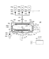
まず、本実施形態にかかる基板処理装置について、図1を用いて説明する。図1はMMT装置として構成された基板処理装置の断面概略図である。
(1) Configuration of Substrate Processing Apparatus First, a substrate processing apparatus according to the present embodiment will be described with reference to FIG. FIG. 1 is a schematic cross-sectional view of a substrate processing apparatus configured as an MMT apparatus.
MMT装置とは、電界と磁界とにより高密度プラズマを発生できる変形マグネトロン型プラズマ源(Modified Magnetron Typed Plasma Source)を用い、例えばシリコン等からなる基板としてのウエハ200をプラズマ処理する装置である。MMT装置は、処理ガスをプラズマ状態として励起させて、例えばウエハ200の表面又はウエハ200に形成された薄膜を酸化や窒化したり、ウエハ200上に薄膜を形成したり、ウエハ200の表面をエッチングしたりする等、各種のプラズマ処理を施すことができる。
The MMT apparatus is an apparatus for plasma processing a
MMT装置は、一般のプラズマ装置と比較して、印加する高周波電力の周波数が10分の1程度であっても効率よくプラズマを発生することが可能である。これにより、プラズマが形成される処理室201へのダメージを低減することができることに加え、パーティクルの発生を抑制することができる。また、後述するサセプタ217へのバイアス印加調整により圧力や供給電力などのプラズマ条件をさほど変更しなくとも、2nm〜15nm程度の幅広い膜厚を有するウエハ200を処理することができる。また、後述するサセプタ217が備えるヒータ217bによって、ウエハ200の加熱温度を室温から700℃まで制御可能である。このようなMMT装置の特徴を生かし、例えば650℃以下の低温領域でCVD法によりウエハ200上に成膜された薄膜の基板処理(改質処理)を、ウエハ200の加熱温度や膜厚を調整しながら行うことができる。
Compared with a general plasma apparatus, the MMT apparatus can efficiently generate plasma even when the frequency of the applied high frequency power is about 1/10. Thereby, in addition to reducing damage to the
(処理室)
本実施形態にかかる基板処理装置100の処理室201を構成する処理容器203は、第1の容器であるドーム型の上側容器210と、第2の容器である碗型の下側容器211と、を備えている。そして、上側容器210が下側容器211の上に被さることにより、処理室201が形成される。上側容器210は例えば酸化アルミニウム(Al2O3)又は石英(SiO2)等の非金属材料で形成されており、下側容器211は例えばアルミニウム(Al)等で形成されている。
(Processing room)
The
下側容器211の側壁には、仕切弁としてのゲートバルブ244が設けられている。ゲートバルブ244が開いている時には、搬送機構(図中省略)を用いて処理室201内へウエハ200を搬入し、または処理室201外へとウエハ200を搬出することができるようになっている。そして、ゲートバルブ244を閉めることにより、処理室201内を気密に閉塞することができるようになっている。
A
(基板支持部)
処理室201内の底側中央には、ウエハ200を支持する基板支持部としてのサセプタ217が配置されている。サセプタ217は、ウエハ200の金属汚染を低減することができるように、例えば、窒化アルミニウム(AlN)、セラミックス、石英等の非金属材料で形成されている。なお、サセプタ217は、下側容器211とは電気的に絶縁されている。
(Substrate support part)
A
サセプタ217の内部には、インピーダンスを変化させるインピーダンス制御電極217cが装備されている。この電極は、インピーダンス制御装置274を介して設置されている。インピーダンス制御装置274には、コイルや可変コンデンサを備えており、コイルのパターン数や可変コンデンサの容量値を制御することにより、インピーダンス制御電
極217c及びサセプタ217を介してウエハ200の電位を制御できるようになっている。なお、インピーダンス制御装置274には、後述する制御部221が電気的に接続されている。
Inside the
サセプタ217には、サセプタ217を昇降させるサセプタ昇降機構268が設けられている。サセプタ217には、貫通孔217aが設けられている。上述の下側容器211底面には、ウエハ200を突き上げるウエハ突き上げピン266が、少なくとも3箇所設けられている。そして、貫通孔217a及びウエハ突き上げピン266は、サセプタ昇降機構268によりサセプタ217が下降させられた時に、ウエハ突き上げピン266がサセプタ217とは非接触な状態で貫通孔217aを突き抜けるように、互いに配置されている。
The
(加熱部)
サセプタ217の内部には、加熱部としてのヒータ217bが一体的に埋め込まれており、ウエハ200を加熱できるようになっている。ヒータ217bに電力が供給されると、ウエハ200の表面が所定温度(例えば室温〜700℃程度)にまで加熱されるようになっている。なお、サセプタ217には、温度センサ(図中省略)が設けられている。ヒータ217b及び温度センサには、後述するコントローラ221が電気的に接続されている。コントローラ221は、温度センサにより検出された温度情報に基づいてヒータ217bへの供給電力を制御するように構成されている。
(Heating part)
Inside the
(ガス供給部)
処理室201の上部には、処理室201内へ処理ガスを供給するシャワーヘッド236が設けられている。シャワーヘッド236は、キャップ状の蓋体233、ガス導入部234、バッファ室237、遮蔽プレート240及びガス吹出口239を備えている。
(Gas supply part)
A
蓋体233は、上側容器210の上部に開設された開口に気密に設けられている。蓋体233の下部には、遮蔽プレート240が設けられている。蓋体233と遮蔽プレート240との間に形成される空間がバッファ室237である。バッファ室237は、ガス導入部234より導入される処理ガスを分散する分散空間として機能する。そして、バッファ室237を通過した処理ガスが、遮蔽プレート240の側部のガス吹出口239から処理室201内に供給されるように構成されている。また、蓋体233には、開口が設けられている。蓋体233の開口には、ガス導入部234の下流端が気密に設けられている。ガス導入部234の上流端には、封止部材としてのOリング203bを介して、ガス供給管232の下流端が接続されている。
The
ガス供給管232の上流側には、処理ガスとしての酸素原子を含むガス(以下、「酸素含有ガス」とも言う。)であるO2ガスを供給する酸素含有ガス供給管232aの下流端と、処理ガスとしての窒素原子を含むガス(以下、「窒素含有ガス」とも言う。)であるN2ガスを供給する窒素含有ガス供給管232bの下流端と、不活性ガスとしての希ガスである例えばArガスを供給する希ガス供給管232cの下流端と、が合流するように接続されている。ガス供給管232、酸素含有ガス供給管232a、窒素含有ガス供給管232b、希ガス供給管232cは、例えば石英、酸化アルミニウム等の非金属材料、及びSUS等の金属材料等により構成されている。
On the upstream side of the
酸素含有ガス供給管232aには、酸素ガス供給源250a、流量制御装置としてのマスフローコントローラ252a及び開閉弁であるバルブ253aが上流から順に接続されている。窒素含有ガス供給管232bには、窒素ガス供給源250b、流量制御装置としてのマスフローコントローラ252b及び開閉弁であるバルブ253bが上流から順に接続されている。希ガス供給管232cには、Arガス供給源250c、流量制御装置とし
てのマスフローコントローラ252c及び開閉弁であるバルブ253cが上流から順に接続されている。
An oxygen
マスフローコントローラ252a〜252c及びバルブ253a〜253cには、後述するコントローラ221が電気的に接続されている。コントローラ221は、処理室201内に供給するガスの流量が所定の流量となるように、マスフローコントローラ252a〜252c及びバルブ253a〜253cの開閉を制御するように構成されている。このように、バルブ253a〜253cを開閉させることにより、マスフローコントローラ252a〜252cにより流量制御しながら、ガス供給管232、バッファ室237及びガス吹出口239を介して処理室201内に、O2ガス又はN2ガスの少なくともいずれかと、Arガスとを自在に供給できるように構成されている。
A
主に、シャワーヘッド236、Oリング203b、ガス供給管232、酸素含有ガス供給管232a、窒素含有ガス供給管232b、希ガス供給管232c、マスフローコントローラ252a〜252c、及びバルブ253a〜253cにより、本実施形態に係るガス供給部が構成されている。なお、酸素ガス供給源250a、窒素ガス供給源250b、Arガス供給源250cをガス供給部に含めて考えてもよい。
Mainly by the
(排気部)
下側容器211の側壁下方には、処理室201内から処理ガス等を排気するガス排気口235が設けられている。ガス排気口235には、ガスを排気するガス排気管231の上流端が接続されている。ガス排気管231には、圧力調整器であるAPC242、開閉弁であるバルブ243、排気装置である真空ポンプ246が、上流から順に設けられている。APC242、バルブ243、真空ポンプ246には、後述するコントローラ221が電気的に接続されている。真空ポンプ246を作動させ、バルブ243を開けることにより、処理室201内を排気することが可能なように構成されている。また、ガス排気管231には、圧力センサ(図中省略)が設けられ、後述するコントローラ221に電気的に接続されている。圧力センサにより検出された圧力情報に基づいて、APC242の開度を調整することにより、処理室201内の圧力値を調整できるように構成されている。主に、ガス排気口235、ガス排気管231、APC242、バルブ243により、本実施形態に係る排気部が構成されている。なお、真空ポンプ246を排気部に含めて考えてもよい。
(Exhaust part)
A
(励起部)
処理容器203(上側容器210)の外周には、処理室201内のプラズマ生成領域224を囲うように、プラズマ生成電極としての筒状電極215が設けられている。筒状電極215は、筒状、例えば円筒状に形成されている。筒状電極215は、インピーダンスの整合を行う整合器272を介して、高周波電力を発生する高周波電源273に接続されている。筒状電極215は、処理室201内に供給されてウエハ200の表面に供給される処理ガスを励起させる放電機構として機能する。
(Excitation part)
A
筒状電極215の外側表面の上下端部には、上部磁石216a及び下部磁石216bがそれぞれ取り付けられている。上部磁石216a及び下部磁石216bは、それぞれ筒状、例えばリング状に形成された永久磁石として構成されている。上部磁石216a及び下部磁石216bは、処理室201の半径方向に沿った両端(すなわち、各磁石の内周端及び外周端)にそれぞれ磁極を有している。上部磁石216a及び下部磁石216bの磁極の向きは、互いに逆向きになるよう配置されている。すなわち、上部磁石216a及び下部磁石216bの内周部の磁極同士は異極となっている。これにより、筒状電極215の内側表面に沿って、円筒軸方向の磁力線が形成されている。
An
処理室201内にO2ガス又はN2ガスの少なくともいずれかを供給した後、上部磁石216a及び下部磁石216bを用いて磁界が形成されたところに、筒状電極215に対して高周波電力を印加して電界を形成することにより、処理室201内のプラズマ生成領域224にマグネトロン放電プラズマが生成されるように構成されている。この際、放出された電子を上述の電界及び磁界が周回運動させることにより、プラズマの電離生成率が高まり、長寿命の高密度プラズマを生成させることができる。
After supplying at least one of O 2 gas and N 2 gas into the
主に、筒状電極215、上部磁石216a、下部磁石216bにより、本実施形態に係る励起部が構成されている。なお、整合器272、高周波電源273を励起部に含めて考えてもよい。
The excitation unit according to this embodiment is mainly configured by the
なお、筒状電極215、上部磁石216a、及び下部磁石216bの周囲には、これらが形成する電界及び磁界が外部環境や他処理炉等の装置に悪影響を及ぼさないように、電界及び磁界を有効に遮蔽する金属製の遮蔽板223が設けられている。
It should be noted that the electric field and the magnetic field are effective around the
(制御部)
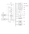
図11に示すように、制御部としてのコントローラ221は、CPU(Central
Processing Unit)221a、RAM(Random Access Memory)221b、記憶装置221c、I/Oポート221dを備えたコンピュータとして構成されている。RAM221b、記憶装置221c、I/Oポート221dは、内部バス221eを介して、CPU221aとデータ交換可能なように構成されている。コントローラ221には、入出力装置225として、例えばタッチパネル、マウス、キーボード、操作端末等が接続されていてもよい。また、コントローラ221には、表示部として、例えばディスプレイ等が接続されていてもよい。
(Control part)
As shown in FIG. 11, the
The computer includes a processing unit (221), a RAM (Random Access Memory) 221b, a
記憶装置221cは、例えばフラッシュメモリ、HDD(Hard Disk Drive)、CD−ROM等で構成されている。記憶装置221c内には、基板処理装置100の動作を制御する制御プログラムや、基板処理の手順や条件などが記載されたプロセスレシピ等が、読み出し可能に格納されている。なお、プロセスレシピは、後述する基板処理工程における各手順をコントローラ221に実行させ、所定の結果を得ることが出来るように組み合わされたものであり、プログラムとして機能する。以下、このプロセスレシピや制御プログラム等を総称して、単にプログラムともいう。なお、本明細書においてプログラムという言葉を用いた場合は、プロセスレシピ単体のみを含む場合、制御プログラム単体のみを含む場合、または、その両方を含む場合がある。また、RAM221bは、CPU221aによって読み出されたプログラムやデータ等が一時的に保持されるメモリ領域(ワークエリア)として構成されている。
The
I/Oポート221dは、上述のマスフローコントローラ252a〜252c、バルブ253a〜253c,243、ゲートバルブ244、APCバルブ242、真空ポンプ246、ヒータ217b、整合器272、高周波電源273、サセプタ昇降機構268、インピーダンス制御装置274等に接続されている。
The I /
CPU221aは、記憶装置221cから制御プログラムを読み出して実行すると共に、入出力装置225からの操作コマンドの入力等に応じて記憶装置221cからプロセスレシピを読み出すように構成されている。そして、CPU221aは、読み出したプロセスレシピの内容に沿うように、信号線Aを通じてAPCバルブ242の開度調整動作、バルブ243の開閉動作、及び真空ポンプ246の起動・停止を、信号線Bを通じてサセプタ昇降機構268の昇降動作を、信号線Cを通じて温度センサに基づくヒータ217bへの供給電力量調整動作(温度調整動作)やインピーダンス制御装置274によるインピーダンス値調整動作を、信号線Dを通じてゲートバルブ244の開閉動作を、信号線Eを通
じて整合器272及び高周波電源273の動作を、信号線Fを通じてマスフローコントローラ252a〜252cによる各種ガスの流量調整動作、及びバルブ253a〜253cの開閉動作を、それぞれ制御するように構成されている。
The
なお、コントローラ221は、専用のコンピュータとして構成されている場合に限らず、汎用のコンピュータとして構成されていてもよい。例えば、上述のプログラムを格納した外部記憶装置(例えば、磁気テープ、フレキシブルディスクやハードディスク等の磁気ディスク、CDやDVD等の光ディスク、MO等の光磁気ディスク、USBメモリやメモリカード等の半導体メモリ)226を用意し、係る外部記憶装置226を用いて汎用のコンピュータにプログラムをインストールすること等により、本実施形態に係るコントローラ221を構成することができる。なお、コンピュータにプログラムを供給するための手段は、外部記憶装置226を介して供給する場合に限らない。例えば、インターネットや専用回線等の通信手段を用い、外部記憶装置226を介さずにプログラムを供給するようにしてもよい。なお、記憶装置221cや外部記憶装置226は、コンピュータ読み取り可能な記録媒体として構成される。以下、これらを総称して、単に記録媒体ともいう。なお、本明細書において記録媒体という言葉を用いた場合は、記憶装置221c単体のみを含む場合、外部記憶装置226単体のみを含む場合、または、その両方を含む場合がある。
The
(2)基板処理工程
続いて、本実施形態にかかる半導体製造工程の一工程として実施される基板処理工程について、図2を用いて説明する。かかる工程は、MMT装置として構成された上述の基板処理装置100により実施される。ここでは、所定の成膜温度で成膜された酸化シリコン膜(SiO2膜)を備えるウエハ200を、プラズマを用いて処理する例について説明する。すなわち、ウエハ200上に形成されたSiO2膜を改質処理して、SiO2膜中の不純物を除去する例について説明する。なお、以下の説明において、基板処理装置100を構成する各部の動作は、コントローラ221により制御される。
(2) Substrate Processing Step Next, the substrate processing step performed as one step of the semiconductor manufacturing process according to the present embodiment will be described with reference to FIG. Such a process is performed by the above-described
(基板搬入・載置工程(S10))
まず、ウエハ200の搬送位置までサセプタ217を下降させ、サセプタ217の貫通孔217aにウエハ突き上げピン266を貫通させる。その結果、突き上げピン266が、サセプタ217表面よりも所定の高さ分だけ突出した状態となる。続いて、ゲートバルブ244を開き、図中省略の搬送機構を用いて処理室201内にウエハ200を搬入する。その結果、ウエハ200は、サセプタ217の表面から突出したウエハ突き上げピン266上に水平姿勢で支持される。
(Substrate loading / placement process (S10))
First, the
なお、ウエハ200上にはSiO2膜が所定の成膜温度でCVD法により予め形成されている。SiO2膜の形成は、例えばテトラエトキシシラン(Si(OC2H5)4、略称:TEOS)等の有機原料ガスを含む成膜ガスと酸素(O2)ガス等の酸化剤とを用い、ウエハ200を所定の成膜温度以下、好ましくは650℃以下の低温領域で加熱して図示しない他のCVD装置により行われる。このように、上記TEOSの例に限らず、低温領域の成膜温度でCVD法により形成されたSiO2膜中には、炭素(C)原子、水素(H)原子、窒素(N)原子、塩素(Cl)原子の少なくともいずれかを含む不純物が残留している場合がある。以下の説明では、ウエハ200上に形成された薄膜の成膜温度を例えば450℃としている。
A SiO 2 film is formed in advance on the
処理室201内にウエハ200を搬入したら、搬送機構を処理室201外へ退避させ、ゲートバルブ244を閉じて処理室201内を密閉する。そして、サセプタ昇降機構268を用いてサセプタ217を上昇させる。その結果、ウエハ200はサセプタ217の上面に配置される。その後、サセプタ217を所定の位置まで上昇させて、ウエハ200を
所定の処理位置まで上昇させる。
When the
なお、ウエハ200を処理室201内に搬入する際には、排気部により処理室201内を排気しつつ、ガス供給部から処理室201内にパージガスとしてのArガスを供給することが好ましい。すなわち、真空ポンプ246を作動させ、バルブ243を開けることにより、処理室201内を排気しつつ、バルブ253cを開けることにより、バッファ室237を介して処理室201内にArガスを供給することが好ましい。これにより、処理室201内へのパーティクルの侵入や、ウエハ200上へのパーティクルの付着を抑制することが可能となる。なお、真空ポンプ246は、少なくとも基板搬入・載置工程(S10)から後述する基板搬出工程(S60)が終了するまでの間は、常に作動させた状態とする。
Note that when the
(昇温・圧力調整工程(S20))
続いて、サセプタ217の内部に埋め込まれたヒータ217bに電力を供給し、ウエハ200の表面を加熱する。ウエハ200の表面温度は、ウエハ200上に予め形成された薄膜の上述の成膜温度以下の温度となるように加熱する。なお、ウエハ200上に複数の薄膜が予め形成されている場合には、最も低い温度で形成された薄膜の成膜温度以下の温度となるように加熱することが好ましい。この際、ヒータ217bの温度は、図中省略の温度センサにより検出された温度情報に基づいてヒータ217bへの供給電力を制御することによって調整される。
(Temperature increase / pressure adjustment step (S20))
Subsequently, power is supplied to the
ウエハ200の加熱処理では、ウエハ200の表面温度を、ウエハ200上に予め形成された薄膜の成膜温度よりも高い温度にまで加熱すると、例えばウエハ200の表面に形成されたソース領域やドレイン領域等に拡散が生じ、回路特性が劣化し、半導体装置の性能が低下してしまう場合がある。ウエハ200の温度を上述のように制限することにより、ウエハ200の表面に形成されたソース領域やドレイン領域における不純物の拡散、回路特性の劣化、半導体装置の性能の低下を抑制できる。なお、上述のようにウエハ200に予め形成された薄膜の成膜温度を450℃としたので、以下の説明では、ウエハ200の表面の加熱温度を、例えば450℃と薄膜の成膜温度と同等の温度に設定している。
In the heat treatment of the
また、処理室201内が所望の圧力(例えば1Pa〜260Pa、好ましくは10Pa〜100Pa)となるように、処理室201内を真空ポンプ246によって真空排気する。この際、処理室201内の圧力は図中省略の圧力センサで測定され、この測定された圧力に基づきAPC242の開度をフィードバック制御する。
Further, the inside of the
(改質処理工程(S30))
ここでは、処理ガスとしてO2ガスを用いる例を説明する。
(Modification process (S30))
Here, an example in which O 2 gas is used as the processing gas will be described.
まず、バルブ253aを開け、処理ガスであるO2ガスを、酸素含有ガス供給管232aからバッファ室237を介して処理室201内に供給する。このとき、O2ガスの流量が所定の流量となるように、マスフローコントローラ252aにより調整する。
First, the
また、処理ガスであるO2ガスを処理室201内に供給する際には、希ガス供給管232cから不活性ガスとしてのArガスを処理室201内に供給してもよい。すなわち、バルブ253cを開け、マスフローコントローラ252cにより流量調整しつつ、バッファ室237を介して処理室201内へArガスを供給してもよい。
In addition, when supplying O 2 gas, which is a processing gas, into the
処理ガスの供給を開始した後、上部磁石216a及び下部磁石216bによる磁界が形成されている所に、筒状電極215に対して、高周波電源273から整合器272を介して所定の高周波電力(例えば50W〜3000W、好ましくは200W〜1000W)を
印加する。この結果、処理室201内にマグネトロン放電が発生し、ウエハ200の上方のプラズマ生成領域224に高密度プラズマが発生する。このときのインピーダンス制御装置274は、予め所望のインピーダンス値に制御しておく。
After the supply of the processing gas is started, a predetermined high-frequency power (for example, from the high-
上述のように、処理室201内にプラズマを発生させることにより、ウエハ200の加熱温度が例えば650℃以下の低温領域の温度であっても、処理室201内に供給されたO2ガスが励起されて活性化される。そして、励起状態である酸素(O)原子(以下、酸素ラジカル(O*)とも呼ぶ)がウエハ200上に予め形成されたSiO2膜に供給される。
As described above, by generating plasma in the
酸素ラジカル(O*)がSiO2膜に供給されることで、SiO2膜から炭素原子(C)、水素原子(H)、窒素原子(N)、塩素原子(Cl)等の不純物を除去することができる。すなわち、酸素ラジカル(O*)の持つエネルギーは、SiO2膜中に含まれるSi−C、Si−H、Si−N、Si−Clの結合エネルギーよりも高いため、この酸素ラジカル(O*)のエネルギーを酸化処理対象のSiO2膜に与えることで、SiO2膜中に含まれるSi−C、Si−H、Si−N、Si−Cl結合は切り離される。Siとの結合を切り離されたN、H、Cl、Cは膜中から除去され、N2、H2、Cl2、CO2等として排出される。 By oxygen radical (O *) is supplied to the SiO 2 film, a carbon atom of a SiO 2 film (C), hydrogen atom (H), a nitrogen atom (N), the program removes the impurities such as chlorine (Cl) be able to. That is, energy of oxygen radicals (O *) is higher than the Si-C, Si-H, Si-N, bond energy of Si-Cl contained in the SiO 2 film, the oxygen radicals (O *) By applying this energy to the SiO 2 film to be oxidized, the Si—C, Si—H, Si—N, and Si—Cl bonds contained in the SiO 2 film are cut off. N, H, Cl, and C that have been separated from the bond with Si are removed from the film and discharged as N 2 , H 2 , Cl 2 , CO 2, and the like.
また、N、H、Cl、Cとの結合が切られることで余ったSiの結合手は、酸素ラジカル(O*)に含まれるOと結びつきSi−O結合が形成され、このとき、SiO2膜は緻密化されることとなる。 Further, the remaining Si bonds due to the disconnection of N, H, Cl, and C are combined with O contained in the oxygen radical (O * ) to form a Si—O bond. At this time, SiO 2 The film will be densified.
また、酸素ラジカル(O*)がSiO2膜に供給されることで、SiO2膜中にて元々欠乏している酸素(O)原子が補われ、SiO2膜の組成比がより化学量論的な組成比を有する膜(ストイキオメトリな膜)となる。すなわち、本実施形態の処理シーケンスにより処理したSiO2膜中の水素原子(H)、炭素原子(C)、窒素原子(N)、塩素原子(Cl)等の不純物の濃度が極めて低く、Si/Oの原子数の比率が化学量論的な組成比である0.5にきわめて近い、良質な膜となる。このようにしてSiO2膜の改質が行われる。 In addition, by oxygen radical (O *) is supplied to the SiO 2 film, the oxygen (O) atoms supplemented that originally deficient in SiO 2 film, the composition ratio of SiO 2 film is more stoichiometric A film having a specific composition ratio (stoichiometric film). That is, the concentration of impurities such as hydrogen atoms (H), carbon atoms (C), nitrogen atoms (N), chlorine atoms (Cl) in the SiO 2 film processed by the processing sequence of this embodiment is extremely low, and Si / A good quality film is obtained in which the ratio of the number of O atoms is very close to 0.5, which is the stoichiometric composition ratio. In this way, the SiO 2 film is modified.
所定の処理時間、例えば1分〜5分が経過し、SiO2膜の改質が終了したら、筒状電極215に対する電力供給を停止する。そして、バルブ253aを閉めて処理室201内へのO2ガスの供給を停止する。
When a predetermined processing time, for example, 1 to 5 minutes elapses and the modification of the SiO 2 film is completed, the power supply to the
(パージ工程(S40))
上述の改質処理工程(S30)が完了した後、バルブ243を開けたままとし、ガス排気管231による排気を継続し、処理室201内の残留ガス等を排出する。すなわち、処理室201内の処理ガスの濃度が所定値以下となるまで、処理室201内を排気して残留ガス等を排出する。例えば、ウエハ200を処理室201の外へ搬出する後述の基板搬出工程(S60)を行うことができる処理ガス濃度になるまで処理室201内を排気する。また、例えば、少なくともウエハ200の表面上から処理ガスがなくなるまで処理室201内を排気するようにしてもよい。このとき、バルブ253cを開き、処理室201内にパージガスとしてのArガスを供給することで、処理室201内からの残留ガスの排出を促すことができる。
(Purge process (S40))
After the above-described reforming process (S30) is completed, the
(降温・大気圧復帰工程(S50))
パージ工程(S40)が完了したら、APC242の開度を調整し、処理室201内の圧力を大気圧に復帰させつつ、ウエハ200を所定の温度(例えば室温〜100℃)に降温させる。具体的には、バルブ253cを開けたままとして、処理室201内に不活性ガ
スであるArガスを供給しつつ、図中省略の圧力センサにより検出された圧力情報に基づいて排気部のAPC242及びバルブ243の開度を制御し、処理室201内の圧力を大気圧に昇圧する。そして、ヒータ217bの供給電力を制御して、ウエハ200の温度を降温させる。
(Cooling / atmospheric pressure recovery process (S50))
When the purge step (S40) is completed, the opening degree of the
(基板搬出工程(S60))
そして、サセプタ217をウエハ200の搬送位置まで下降させ、サセプタ217の表面から突出させたウエハ突き上げピン266上にウエハ200を支持させる。そして、ゲートバルブ244を開き、図中省略の搬送機構を用いてウエハ200を処理室201の外へ搬出し、本実施形態に係る基板処理工程を終了する。なお、上記において、ウエハ200の温度、処理室201内の圧力、各ガスの流量、筒状電極215に印加する電力、処理時間等の条件等は、改質対象の膜の材料や膜厚等によって任意に調整する。
(Substrate unloading step (S60))
Then, the
(3)本実施形態に係る効果
本実施形態によれば、以下に示す1つまたは複数の効果を奏する。
(3) Effects according to the present embodiment According to the present embodiment, the following one or more effects are achieved.
(a)本実施形態によれば、ヒータ217bによりウエハ200を加熱し、ガス供給部により供給させた処理ガスを励起部により励起し、励起した処理ガスをウエハ200の表面に供給して処理する際、ウエハ200の温度がウエハ200上に予め形成された薄膜の成膜温度以下の温度となるように、ヒータ217bの温度を調整している。これにより、低いサーマルバジェットで、ウエハ200上に低温領域で予め形成された薄膜を改質でき、炭素原子(C)、水素原子(H)、窒素原子(N)等の不純物を薄膜中から除去することができる。
(A) According to this embodiment, the
(b)本実施形態によれば、励起部としてプラズマ生成電極を備えている。これにより、ウエハ200を加熱するヒータ217bの温度が低温領域の温度であっても、ウエハ200上に予め形成された薄膜を改質し、膜質を向上させることができる。すなわち、ウエハ200の加熱温度は抑制しつつ、ウエハ200に予め形成された膜中の不純物の除去や、結晶構造の改善、欠陥の除去をプラズマの持つエネルギーにより行うことができる。そして、ウエハ200上に形成された薄膜を化学量論的な組成比を有する膜(ストイキオメトリな膜)に改質できる。
(B) According to the present embodiment, the plasma generating electrode is provided as the excitation unit. Thereby, even if the temperature of the
(c)本実施形態によれば、処理室201内にウエハ200を支持するサセプタ217と、サセプタ217の内部に設けられるインピーダンス制御電極217cと、インピーダンス制御電極217cに接続され、インピーダンス制御電極217cのインピーダンスを調整してウエハ200の電位を調整するインピーダンス制御装置274とを備えている。これにより、インピーダンス制御装置274及び励起部を調整することで、励起した処理ガスをウエハ200に供給して処理する際、ウエハ200に対して垂直方向又は水平方向の電界のいずれかの電界を強くすることができる。従って、例えば、ウエハ200上に予め形成された薄膜の処理面に、MOSトランジスタのゲート構造やDRAMのキャパシタ構造等、所定の形状の凹凸構造が予め形成されていてもよい。
(C) According to the present embodiment, the
すなわち、表面に凹凸構造が形成されたウエハ200を処理する場合、ウエハ200に形成された凹凸構造の表面を均一に処理できない場合がある。例えば、ウエハ200の表面の凹部の底部より凹部の側壁部の方が処理の進行が遅くなる場合がある。本発明によれば、インピーダンス制御装置274を所定のインピーダンス値に制御することにより、例えば、ウエハ200に対して、垂直方向の電界よりも水平方向の電界を高めることができ、凹部の側壁部の処理速度を向上させることができる。また、例えば、ウエハ200に対して、水平方向の処理速度よりも垂直方向の処理速度を高めることもできる。このように、凹部の底部及び側壁部への処理速度(すなわち水平方向及び垂直方向の両方向の処理速
度)を均一にし、凹凸構造の表面への均一な処理を施すことができる。
That is, when processing the
(d)本実施形態によれば、ウエハ200上に予め形成された薄膜の成膜温度を650℃以下、例えば450℃としている。そして、薄膜を備えるウエハ200を加熱するヒータ217bの温度を、薄膜の成膜温度以下の温度、例えば薄膜の成膜温度と同等の温度である450℃としている。これにより、ウエハ200上に予め形成された薄膜に加わる熱ストレスの発生を抑制させて、基板処理(改質処理)を行うことができる。
(D) According to the present embodiment, the film forming temperature of the thin film previously formed on the
<本発明の他の実施形態>
以上、本発明の実施形態を具体的に説明したが、本発明は上述の実施形態に限定されるものではなく、その要旨を逸脱しない範囲で種々変更可能である。
<Other Embodiments of the Present Invention>
As mentioned above, although embodiment of this invention was described concretely, this invention is not limited to the above-mentioned embodiment, It can change variously in the range which does not deviate from the summary.
上述の実施形態では、ウエハ200上に形成された薄膜が、例えば650℃以下の低温領域でCVD法により成膜される場合を説明したが、本発明はこれに限定されるものではない。すなわち、ウエハ200上に予め形成される薄膜は、例えば、プラズマCVDにより成膜されたもの、高温領域でCVD法(HTO:High Temperature Oxide)により成膜されたもの、高温の熱処理(アニール)により成膜されたもの、ALD法により成膜されたもの等であってもよい。なお、HTOはカバレッジ特性が悪いといわれている。
In the above-described embodiment, the case where the thin film formed on the
また、上述の実施形態では、ウエハ200上に酸化膜であるSiO2膜が所定の成膜温度で予め形成されている場合について説明した。本発明はこれに限定されるものではなく、例えば、ウエハ200上にSiN膜等の窒化膜が所定の成膜温度で予め形成されていてもよい。この場合、処理ガスとして、少なくとも窒素含有ガス(N2ガス)を処理室201内に供給することが好ましい。すなわち、図1に示すように、まず、バルブ253bを開け、処理ガスであるN2ガスを、窒素含有ガス供給管232bからバッファ室237を介して処理室201内に供給する。このとき、N2ガスの流量が所定の流量となるように、マスフローコントローラ252bの開度を調整する。窒素ラジカル(N*)は、高いエネルギーを有するため、SiN膜中から水素(H)原子、炭素(C)原子、塩素(Cl)原子等の不純物を脱離させて排出する効果を有する。そして、不純物が脱離することで生じた未結合手に窒素(N)原子が結合し、SiN膜の窒化がより促され、SiN膜の膜質がさらに改善される。また、膜中に窒素(N)原子を導入することによって、不純物の拡散を防止することができる。このように、ウエハ200上に窒化膜が予め形成されている場合であっても、上述の実施形態と同様の効果を得ることができる。
In the above-described embodiment, the case where the SiO 2 film, which is an oxide film, is previously formed on the
また、例えばウエハ200上にSiON膜等、酸窒化膜が所定の成膜温度で予め形成されていてもよい。この場合、処理ガスとして、酸素原子(O)及び窒素原子(N)を含むガスである例えば一酸化窒素(NO)ガスや亜酸化窒素(N2O)ガス等を処理室201内に供給することが好ましい。これにより酸窒化膜中の不純物を除去することができ、上述の実施形態と同様の効果を得ることができる。また、ウエハ200上に予め形成されたSiO2膜を改質する処理ガスとして、一酸化窒素(NO)ガスや亜酸化窒素(N2O)ガス等の酸素原子及び窒素原子を含有するガスを用いてもよい。O2ガス等に比べて、SiO2膜の不純物除去効果は劣るものの、低温領域で形成された膜中の不純物を除去することができる。
Further, for example, an oxynitride film such as a SiON film may be formed on the
また、上述の実施形態では、酸素含有ガスとしてO2ガスを用いる場合を説明したが、本発明はこれに限定されるものではなく、ウエハ200上に形成された薄膜の成膜温度以下の温度で加熱処理を行えば、例えばオゾン(O3)ガスや水蒸気(H2O)を用いて、アニール処理を行ってもよい。また、酸素ガス及び水素ガスを処理室201内に供給してアニール処理を施してもよく、BIO処理を施してもよい。
In the above embodiment, the case where O 2 gas is used as the oxygen-containing gas has been described. However, the present invention is not limited to this, and the temperature is equal to or lower than the film forming temperature of the thin film formed on the
また、上述の実施形態では、有機原料ガスを含む成膜ガスであるTEOSを用いてウエハ200上にSiO2膜が予め形成されている。本発明は、これに限定されるものではなく、例えばDCSやTSA等の有機原料ガスを含む成膜ガス等を用い、水素(H)原子、炭素(C)原子、窒素(N)原子又は塩素(Cl)原子の少なくともいずれかを含む薄膜が、ウエハ200上に予め形成されていてもよい。これにより、例えば薄膜に上述の実施形態と同様の処理が施されることにより、薄膜中の不純物を低減する効果を得ることができる。
In the above-described embodiment, the SiO 2 film is formed in advance on the
また、上述した実施形態では、サセプタ217の内部に設けたヒータ217bによってウエハ200を加熱するようにしていたが、本発明はこのような形態に限定されない。例えば、図8に例示するように、ヒータ217bに加えて、ランプ加熱ユニット280からも赤外線等を照射することでウエハ200を加熱するようにしてもよい。この場合、ランプ加熱機構280は、処理室201の上方、つまり上側容器210の上面に設けられた光透過窓278を介して処理室201内に光を照射するような構成とするとよい。また、ヒータ217bとランプ加熱ユニット280とを併用することで、ヒータ217bのみを用いて加熱する場合と比較して、より短時間でウエハ200を昇温させることが可能である。また、ヒータ217bを設けずに、ランプ加熱ユニット280のみを用いてウエハ200を加熱するようにしてもよい。なお、ランプ加熱ユニット280は、信号線Gを通じて制御部221により制御するように構成されている。
In the above-described embodiment, the
また、上述した実施形態では、MMT装置として構成された基板処理装置100を用いて実施する場合を説明したが、本発明は、それに限らずその他の装置、例えばICP(Inductively Coupled Plasma)装置、ECR(Electron Cyclotron Resonance)装置を用いても実施可能である。
In the above-described embodiment, the case where the
図9は、本発明の他の実施形態に係る基板処理装置であるICP方式プラズマ処理装置300を示している。本実施形態にかかる構成の詳細な説明は、前記実施形態と同様の機能を有する構成要件に同一の符号を付して省略する。また、ガス供給部についても図示を省略している。本実施形態に係るICP方式プラズマ処理装置300は、整合器272a、272b、高周波電源273a、273b及び誘電コイル315a,315bを介してそれぞれ電力が供給されることで、プラズマが生成される。誘電コイル315aは、処理容器203の天井側の外側に敷設されている。誘電コイル315bは、処理容器203の外周壁の外側に敷設されている。本実施形態においても、酸素原子又は窒素原子の少なくともいずれかを含む処理ガスをガス供給管232から、ガス導入部234を経由して処理室201内へ供給する。また、ガス供給と前後して、励起部である誘電コイル315a,315bへ高周波電力を流すと、電磁誘導により電界が生じる。この電界をエネルギーとして、供給された処理ガスをプラズマ状態として励起させて、活性種を生成することができる。
FIG. 9 shows an ICP
図10は、本発明の更に他の実施形態に係る基板処理装置であるECR方式プラズマ処理装置400を示している。本実施形態にかかる構成の詳細な説明は、前記実施形態と同様の機能を有する構成要件に同一の符号を付して省略する。また、ガス供給部についても図示を省略している。本実施形態に係るECR方式プラズマ処理装置400は、マイクロ波を供給してプラズマを生成する整合器272b、高周波電源273b、マイクロ波導入管415a及び誘電コイル415bを備えている。マイクロ波導入管415aは、処理容器203の天井壁に敷設されている。誘電コイル415bは、処理容器203の外周壁の外側に敷設されている。本実施形態においても、酸素原子又は窒素原子の少なくともいずれかを含む処理ガスをガス供給管232から、ガス導入部234を経由して処理室201内へ供給する。また、ガス供給と前後して、マイクロ波導入管415aへマイクロ波41
8aを導入し、マイクロ波418aを処理室201へ放射させる。このマイクロ波418aと、誘電コイル415bからの高周波電力とにより、供給された処理ガスをプラズマ状態として励起させ、活性種を生成することができる。なお、マイクロ波として、例えば可変周波数マイクロ波(VFM)、固定周波数マイクロ波(FFM)等を用いることができる。
FIG. 10 shows an ECR
8 a is introduced, and the
この他、RTP(Rapid Thermal Processing)装置を用いたり、紫外線を照射することで、ウエハ200上に予め形成された薄膜の改質処理を行ってもよい。
In addition, a thin film reforming process previously formed on the
次に、本発明の実施例を図3〜図7を参照しながら説明する。本実施例として、成膜ガスとしてTEOSを用い、低温領域の成膜温度(450℃)で、SiO2膜が予め形成されたウエハ200を用い、このウエハ200にプラズマ生成電極により励起させた酸素ガス(O2ガス)を供給して基板処理、すなわち改質処理を施す場合について説明する。
Next, an embodiment of the present invention will be described with reference to FIGS. In this embodiment, TEOS is used as a film forming gas, and a
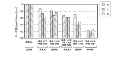
図3は、希フッ酸(DHF)によるエッチングが施された場合において、各条件にて改質処理が施されたSiO2膜のエッチングレートの評価結果を示すグラフ図である。図4は、各条件で基板処理を施したウエハのSiO2膜中のXPS(X−ray photoelectron spectroscopy)分析による酸素及びシリコンの原子数の比率を示すグラフ図である。図5は、各条件で基板処理を施したウエハのSiO2膜中のXPS分析によるシリコン2pと酸素1sの半値幅を示すグラフ図である。図6は、SiO2膜が形成されたウエハのSIMS(Secondary Ion Mass Spectrometry)により測定したSiO2膜中の不純物濃度を示すグラフ図である。図7は、ウエハ上のシリコン酸化膜(SiO2膜)の欠陥密度を示すグラフ図である。 FIG. 3 is a graph showing the evaluation results of the etching rate of the SiO 2 film subjected to the modification treatment under each condition when etching with dilute hydrofluoric acid (DHF) is performed. FIG. 4 is a graph showing the ratio of the number of oxygen and silicon atoms by XPS (X-ray photoelectron spectroscopy) analysis in the SiO 2 film of the wafer subjected to substrate processing under each condition. FIG. 5 is a graph showing the half width of silicon 2p and oxygen 1s by XPS analysis in the SiO 2 film of the wafer subjected to substrate processing under each condition. FIG. 6 is a graph showing the impurity concentration in the SiO 2 film measured by SIMS (Secondary Ion Mass Spectrometry) of the wafer on which the SiO 2 film is formed. FIG. 7 is a graph showing the defect density of the silicon oxide film (SiO 2 film) on the wafer.
ここで、図3〜図7中の、「温度:80℃、時間:60秒」とは、ウエハ200の加熱温度を80℃とし、処理ガスを60秒間供給してウエハ200の改質処理を行った場合を示す(実施例1)。「温度:450℃、時間:60秒」とは、ウエハ200の加熱温度を450℃、すなわちSiO2膜の成膜温度とほぼ同等の温度とし、処理ガスを60秒間供給してウエハ200の改質処理を行った場合を示す(実施例2)。「温度:450℃、バイアス高、時間:60秒」とは、ウエハ200の加熱温度を450℃とし、他の実施例よりもバイアスを高めて、処理ガスを60秒間供給してウエハ200の改質処理を行った場合を示す(実施例3)。「温度:450℃、時間:120秒」とは、ウエハ200の加熱温度を450℃とし、処理ガスを120秒間供給してウエハ200の改質処理を行った場合を示す(実施例4)。
Here, “temperature: 80 ° C., time: 60 seconds” in FIGS. 3 to 7 means that the heating temperature of the
また、「温度:650℃、時間:60秒」とは、ウエハ200の加熱温度をSiO2膜の成膜温度よりも高い650℃とし、処理ガスを60秒間供給してウエハ200の改質処理を行った場合を示す(参考例1)。さらに、図7中の「アニール処理、温度:450℃」とは、O2ガスを励起させずに、温度450℃でアニール処理(熱処理)を施してウエハ200の改質処理を行った場合を示す(参考例2)。
“Temperature: 650 ° C., time: 60 seconds” means that the heating temperature of the
また、「処理なし」とは、ウエハ200に改質処理を行っていない場合を示し、比較例とした。
“No treatment” indicates a case where the
図3によれば、比較例のエッチングレートを1.0としたとき、実施例1では、エッチングレートが約0.8倍まで改善したことが分かる。実施例2では、エッチングレートが約0.2倍まで改善したことが分かる。実施例3では、比較例と比較すると、エッチングレートが約0.2倍まで改善するが、実施例2と比較すると、エッチングレートは殆ど変
らないことが分かる。実施例4では、比較例と比較すると、エッチングレートが約0.2倍まで改善するが、実施例2及び実施例3と比較すると、エッチングレートはわずかに改善されるのみであることが分かる。参考例1のように、ウエハ200の温度を成膜温度よりも高くして改質したとしても、特に実施例2〜4と比較すると、エッチングレートは殆ど変らないことが分かる。これらから、ウエハ200に改質処理を行う際は、ウエハ200の加熱温度をウエハ200上に予め形成された薄膜の成膜温度以下とすることがよく、成膜温度とほぼ同等の温度にするとより好ましいことが分かる。
According to FIG. 3, when the etching rate of the comparative example is 1.0, it can be seen that in Example 1, the etching rate was improved to about 0.8 times. In Example 2, it can be seen that the etching rate was improved to about 0.2 times. In Example 3, when compared with the comparative example, the etching rate is improved to about 0.2 times, but when compared with Example 2, it is understood that the etching rate hardly changes. In Example 4, when compared with the comparative example, the etching rate is improved to about 0.2 times, but when compared with Example 2 and Example 3, it can be seen that the etching rate is only slightly improved. It can be seen that even if the temperature of the
図4によれば、ウエハ200上に予め形成されたSiO2膜の改質処理後の膜中のシリコン原子(Si)と酸素原子(O)の原子数の比率が分かる。すなわち、比較例と比較すると、改質処理を施した実施例1、実施例2及び参考例1は、SiO2の理想的な化学量論比(Si:O=1:2)に近づき、結晶構造がよりストイキオメトリになっていることが分かる。これは、シリコン原子(Si)の量が変化することは考えられないので、余分な酸素原子(O)の量が減ったためと考えられる。また、改質前のSiO2膜中の酸素原子(O)が欠乏している場合は、酸素原子(O)が供給されることで、SiO2の理想的な化学量論比に近づけることができると考えられる。
According to FIG. 4, the ratio of the number of atoms of silicon atoms (Si) and oxygen atoms (O) in the film after the reforming process of the SiO 2 film formed in advance on the
図5は、XPSにより測定したSi2p及びO1sのピークの半値幅を示したものである。半値幅が小さいほど結晶構造がより安定していることを示す。すなわち、半値幅が小さいほど、SiO2膜の改質処理後の膜中の結合状態が良いことが分かる。図5によれば、比較例では、Si2pの半値幅が約1.7であり、O1sの半値幅が約1.8であったが、SiO2膜の成膜温度と同等の温度で改質処理を行う実施例2では、Si2pの半値幅が1.65になり、O1sの半値幅が1.6になり、結晶構造が安定して良質の酸化膜となっていることが分かる。なお、参考例では、実施例2と比較して半値幅がさらに小さくなり、改質後のSiO2膜の結晶構造がより安定していることが分かる。 FIG. 5 shows the full width at half maximum of the Si2p and O1s peaks measured by XPS. A smaller half width indicates that the crystal structure is more stable. That is, it can be seen that the smaller the half width is, the better the bonding state in the film after the modification treatment of the SiO 2 film is. According to FIG. 5, in the comparative example, the full width at half maximum of Si2p was about 1.7 and the full width at half maximum of O1s was about 1.8, but the modification was performed at a temperature equivalent to the film formation temperature of the SiO 2 film. In Example 2 where the treatment is performed, the half-value width of Si2p is 1.65 and the half-value width of O1s is 1.6, which indicates that the crystal structure is stable and a high-quality oxide film is obtained. In the reference example, it can be seen that the full width at half maximum is further reduced as compared with Example 2, and the crystal structure of the SiO 2 film after the modification is more stable.
図6は、SIMSにより測定した深さ2nm〜8nmにおけるドーズ量を示しており、比較例の膜中の水素(H)原子、炭素(C)原子、窒素(N)原子の各原子のドーズ量を1.0としたときの実施例1〜4及び参考例1の各原子のドーズ量の比率を示している。図6によれば、プラズマで改質処理を行った実施例1〜4及び参考例1は、改質処理を行わない比較例と比べて、膜中の不純物が減少していることが分かる。すなわち、比較例と比べて、例えば実施例2では、改質処理後のSiO2膜中の水素(H)原子のドーズ量が約0.8倍、炭素(C)原子のドーズ量は約0.7倍、窒素(N)原子のドーズ量は約0.75倍に、不純物が減少していることが分かる。このようにプラズマによる改質処理後のSiO2膜中の不純物が低減しているため、膜質が向上していることが裏付けられ、デバイス特性の向上が期待できる。 FIG. 6 shows dose amounts at a depth of 2 nm to 8 nm measured by SIMS. The dose amounts of hydrogen (H) atoms, carbon (C) atoms, and nitrogen (N) atoms in the film of the comparative example. The ratio of the dose amount of each atom in Examples 1 to 4 and Reference Example 1 is shown. According to FIG. 6, it can be seen that in Examples 1 to 4 and Reference Example 1 in which the modification process is performed with plasma, impurities in the film are reduced as compared with the comparative example in which the modification process is not performed. That is, compared with the comparative example, in Example 2, for example, the dose of hydrogen (H) atoms in the SiO 2 film after the reforming process is about 0.8 times, and the dose of carbon (C) atoms is about 0. It can be seen that impurities are reduced by 0.7 times and the dose of nitrogen (N) atoms is about 0.75 times. Thus, since the impurities in the SiO 2 film after the modification treatment by plasma are reduced, it is confirmed that the film quality is improved, and improvement of device characteristics can be expected.
図7は、ウエハ200上のSiO2膜の欠陥密度を示すグラフ図であり、電気検出ESR(Electron Spin Resonance)により、SiO2膜のトラップ密度の測定結果を示し、デバイス特性改善の指標とした。電気検出ESRとは、通常のESRにマイクロ波による原子スピン操作機能を追加することでESRの測定感度や精度をより高感度にした測定方法である。なお、図7中のSiO2膜中のバルクトラップとは、SiO2膜中の欠陥の測定結果を示したものであり、Si基板/SiO2界面トラップとは、ウエハ200とSiO2膜との界面に存在する欠陥の測定結果を示したものであり、SiO2膜中の酸素欠損とは、SiO2膜中のシリコン原子(Si)が酸素原子(O)と結合していないホール欠損の測定結果を示したものである。図7によれば、ウエハ200上に形成されたSiO2膜中のトラップ密度が、プラズマによる改質処理を施すことで低減していることが分かる。すなわち、SiO2膜中のバルクトラップは、比較例では3E10であったが、実施例2では6E9に低減したことが分かる。また、Si基板/SiO2界面トラップは、比較例では5E11であったが、実施例2では1E11に低減したこ
とが分かる。また、SiO2膜中の酸素欠損は、比較例では7E11であったが、実施例2では検出下限まで低減したことが分かる。なお、参考例2として、プラズマ処理を行わずに、温度450℃でアニール処理(熱処理)を行ってウエハ200の改質処理をした例を示す。このように、O2ガスを励起させることなく、SiO2膜を450℃でアニール処理しても、SiO2膜中のトラップ密度を改善する効果は確認できないことが分かる。これにより、450℃という低温領域の成膜温度で形成されたSiO2膜の改質処理は、加熱温度だけではなく、プラズマ処理することが重要であることが分かり、プラズマ処理により、SiO2膜中の欠陥を低減することができることが分かる。この結果、デバイスのリーク電流の低減が期待でき、デバイス特性の向上が見込まれる。
FIG. 7 is a graph showing the defect density of the SiO 2 film on the
図3〜図7から、SiO2膜の改質効果においては、参考例1が最も良い結果が得られることが分かる。しかしながら、参考例1のように、SiO2膜の成膜温度よりも高い温度で改質処理を行うと、サーマルバジェット等の問題がある。これに対し、実施例1〜実施例4のように、ウエハ200上に低温領域の成膜温度で予め形成された薄膜の成膜温度以下の温度で処理を行っても、薄膜中の不純物の除去効果が得られることが分かる。特に、図3に示す本発明の総合的な改質の効果であるDHFによるエッチングレートは、実施例2〜実施例4のように、薄膜の成膜温度と同等の温度で処理を行っても、参考例1と遜色ない効果を得ることができることに加え、サーマルバジェット等の問題もない。
From FIG. 3 to FIG. 7, it can be seen that the reference example 1 gives the best results in the modification effect of the SiO 2 film. However, when the reforming process is performed at a temperature higher than the deposition temperature of the SiO 2 film as in Reference Example 1, there is a problem such as a thermal budget. On the other hand, even if processing is performed at a temperature lower than the film formation temperature of the thin film previously formed on the
<本発明の好ましい態様>
以下に、本発明の好ましい態様について付記する。
<Preferred embodiment of the present invention>
Hereinafter, preferred embodiments of the present invention will be additionally described.
本発明の一態様によれば、
所定の成膜温度で形成された薄膜を有する基板が搬入される処理室と、
前記処理室内に酸素又は窒素の少なくともいずれかを含む処理ガスを供給するガス供給部と、
前記処理室内に供給された処理ガスを励起する励起部と、
前記処理室内の前記基板を加熱する加熱部と、
前記処理室内を排気する排気部と、
前記加熱部により前記基板を加熱させ、前記ガス供給部により供給された処理ガスを前記励起部により励起させ、励起した処理ガスを前記基板の表面に供給して前記基板を処理する際、前記基板の温度が前記成膜温度以下の温度となるように、少なくとも前記ガス供給部、前記励起部、前記加熱部及び前記排気部を制御する制御部と、を備える基板処理装置が提供される。
According to one aspect of the invention,
A processing chamber into which a substrate having a thin film formed at a predetermined film formation temperature is carried;
A gas supply unit for supplying a processing gas containing at least one of oxygen and nitrogen into the processing chamber;
An excitation unit for exciting the processing gas supplied into the processing chamber;
A heating unit for heating the substrate in the processing chamber;
An exhaust section for exhausting the processing chamber;
When the substrate is processed by heating the substrate by the heating unit, exciting the processing gas supplied by the gas supply unit by the excitation unit, and supplying the excited processing gas to the surface of the substrate. There is provided a substrate processing apparatus comprising: a control unit that controls at least the gas supply unit, the excitation unit, the heating unit, and the exhaust unit such that the temperature of the substrate is equal to or lower than the film formation temperature.
好ましくは、
前記処理室内に設けられ、前記基板を支持する基板支持部と、
前記基板支持部の内部に設けられるインピーダンス制御電極と、
前記インピーダンス制御電極に接続され、前記インピーダンス制御電極のインピーダンスを調整して前記基板の電位を調整するインピーダンス制御装置と、を備え、
前記制御部が、励起した処理ガスを前記基板に供給して前記基板を処理する際、前記基板に対して垂直方向又は水平方向の電界のいずれかの電界が強くなるように、前記インピーダンス制御装置及び前記励起部を制御する。
Preferably,
A substrate support section provided in the processing chamber and supporting the substrate;
An impedance control electrode provided inside the substrate support;
An impedance control device connected to the impedance control electrode and adjusting the potential of the substrate by adjusting the impedance of the impedance control electrode;
When the control unit supplies the excited processing gas to the substrate to process the substrate, the impedance control device is configured so that an electric field in either a vertical direction or a horizontal direction is strong with respect to the substrate. And controlling the excitation unit.
また好ましくは、
前記薄膜は、酸化膜、窒化膜又は酸窒化膜のいずれかである。
Also preferably,
The thin film is any one of an oxide film, a nitride film, and an oxynitride film.
また好ましくは、
前記薄膜の処理面には、所定の形状の凹凸構造が予め形成されている。
Also preferably,
A concavo-convex structure having a predetermined shape is formed in advance on the processing surface of the thin film.
また好ましくは、
前記励起部は、マグネトロン放電により処理ガスを励起させる。
Also preferably,
The excitation unit excites the processing gas by magnetron discharge.
また好ましくは、
前記基板には、マグネトロン放電によって生成された処理ガスの活性種が供給される。
Also preferably,
The substrate is supplied with active species of processing gas generated by magnetron discharge.
また好ましくは、
前記成膜温度は650℃以下である。
Also preferably,
The film forming temperature is 650 ° C. or lower.
また好ましくは、
前記薄膜は、水素原子、炭素原子、窒素原子又は塩素原子の少なくともいずれかを含む。
Also preferably,
The thin film contains at least one of a hydrogen atom, a carbon atom, a nitrogen atom, or a chlorine atom.
本発明の他の態様によれば、
所定の成膜温度で形成された薄膜を有する基板を処理室内に搬入する工程と、
前記基板の温度が前記成膜温度以下の温度となるように前記基板を加熱し、前記処理室内を排気しつつ、前記処理室内に酸素又は窒素の少なくともいずれかを含む処理ガスを供給する工程と、
前記処理室内に供給した処理ガスを励起させ、励起した処理ガスを前記基板の表面に供給して前記基板を処理する工程と、
処理した前記基板を前記処理室内から搬出する工程と、を有する半導体装置の製造方法が提供される。
According to another aspect of the invention,
Carrying a substrate having a thin film formed at a predetermined film formation temperature into a processing chamber;
Supplying the processing gas containing at least one of oxygen and nitrogen into the processing chamber while heating the substrate so that the temperature of the substrate is equal to or lower than the film formation temperature and exhausting the processing chamber; ,
Exciting the processing gas supplied into the processing chamber, supplying the excited processing gas to the surface of the substrate, and processing the substrate;
And a step of unloading the processed substrate from the processing chamber.
本発明の更に他の態様によれば、
所定の成膜温度で形成された薄膜を有する基板を処理室内に搬入する手順と、
前記基板の温度が前記成膜温度以下の温度となるように前記基板を加熱し、前記処理室内を排気しつつ、前記処理室内に酸素又は窒素の少なくともいずれかを含む処理ガスを供給する手順と、
前記処理室内に供給した処理ガスを励起させ、励起した処理ガスを前記基板の表面に供給して前記基板を処理する手順と、
処理した前記基板を前記処理室内から搬出する手順と、をコンピュータに実行させるプログラムが提供される。
According to yet another aspect of the invention,
A procedure for carrying a substrate having a thin film formed at a predetermined film formation temperature into a processing chamber;
Supplying the processing gas containing at least one of oxygen and nitrogen into the processing chamber while heating the substrate so that the temperature of the substrate is equal to or lower than the film formation temperature and exhausting the processing chamber; ,
Exciting the processing gas supplied into the processing chamber, supplying the excited processing gas to the surface of the substrate, and processing the substrate;
A program for causing a computer to execute a procedure for carrying out the processed substrate from the processing chamber is provided.
本発明の更に他の態様によれば、
所定の成膜温度で形成された薄膜を有する基板を処理室内に搬入する手順と、
前記基板の温度が前記成膜温度以下の温度となるように前記基板を加熱し、前記処理室内を排気しつつ、前記処理室内に酸素又は窒素の少なくともいずれかを含む処理ガスを供給する手順と、
前記処理室内に供給した処理ガスを励起させ、励起した処理ガスを前記基板の表面に供給して前記基板を処理する手順と、
処理した前記基板を前記処理室内から搬出する手順と、をコンピュータに実行させるためのプログラムが記録された記録媒体が提供される。
According to yet another aspect of the invention,
A procedure for carrying a substrate having a thin film formed at a predetermined film formation temperature into a processing chamber;
Supplying the processing gas containing at least one of oxygen and nitrogen into the processing chamber while heating the substrate so that the temperature of the substrate is equal to or lower than the film formation temperature and exhausting the processing chamber; ,
Exciting the processing gas supplied into the processing chamber, supplying the excited processing gas to the surface of the substrate, and processing the substrate;
There is provided a recording medium in which a program for causing a computer to execute a procedure for unloading the processed substrate from the processing chamber is provided.
本発明の更に他の態様によれば、
所定の成膜温度で形成された薄膜を有する基板が搬入される処理室と、
前記処理室内に酸素又は窒素の少なくともいずれかを含む処理ガスを供給するガス供給部と、
前記処理室内に供給された処理ガスを励起する励起部と、
前記処理室内の前記基板を加熱する加熱部と、
前記処理室内を排気する排気部と、
前記加熱部により前記基板を加熱させ、前記ガス供給部により供給された処理ガスを前記励起部により励起させ、励起した処理ガスを前記基板の表面に供給して前記基板を処理する際、前記基板の温度が前記成膜温度以下の温度となるように、少なくとも前記ガス供給部、前記励起部、前記加熱部及び前記排気部を制御する制御部と、を備える半導体装置の製造装置が提供される。
According to yet another aspect of the invention,
A processing chamber into which a substrate having a thin film formed at a predetermined film formation temperature is carried;
A gas supply unit for supplying a processing gas containing at least one of oxygen and nitrogen into the processing chamber;
An excitation unit for exciting the processing gas supplied into the processing chamber;
A heating unit for heating the substrate in the processing chamber;
An exhaust section for exhausting the processing chamber;
When the substrate is processed by heating the substrate by the heating unit, exciting the processing gas supplied by the gas supply unit by the excitation unit, and supplying the excited processing gas to the surface of the substrate. There is provided a semiconductor device manufacturing apparatus comprising: a control unit that controls at least the gas supply unit, the excitation unit, the heating unit, and the exhaust unit so that the temperature of the gas is equal to or lower than the film formation temperature. .
200 ウエハ(基板)
201 処理室
217 サセプタ(基板支持部)
217b ヒータ(加熱部)
221 コントローラ(制御部)
231 排気管
200 wafer (substrate)
201
217b Heater (heating unit)
221 Controller (control unit)
231 Exhaust pipe
Claims (7)
前記処理室内に酸素又は窒素の少なくともいずれかを含む処理ガスを供給するガス供給部と、
前記処理室内に供給された処理ガスを励起する励起部と、
前記処理室内の前記基板を加熱する加熱部と、
前記処理室内を排気する排気部と、
前記加熱部により前記基板を、前記不純物を含む薄膜の成膜温度及び前記他の薄膜の成膜温度のうち最も低い成膜温度以下の温度の範囲で予め定められた温度まで加熱させ、前記ガス供給部により供給された処理ガスを前記励起部により励起させるように、前記ガス供給部、前記励起部及び前記加熱部を制御する制御部と、
を備える基板処理装置。 A processing chamber into which a substrate in which a thin film containing an impurity formed at a film forming temperature of 650 ° C. or less and another thin film different from the thin film containing the impurity are previously formed is carried;
A gas supply unit for supplying a processing gas containing at least one of oxygen and nitrogen into the processing chamber;
An excitation unit for exciting the processing gas supplied into the processing chamber;
A heating unit for heating the substrate in the processing chamber;
An exhaust section for exhausting the processing chamber;
The substrate is heated by the heating unit to a predetermined temperature in a range of a temperature equal to or lower than a lowest film forming temperature among a film forming temperature of the thin film containing impurities and a film forming temperature of the other thin film, and the gas A control unit that controls the gas supply unit, the excitation unit, and the heating unit so that the processing gas supplied by the supply unit is excited by the excitation unit;
A substrate processing apparatus comprising:
前記基板支持部の内部に設けられるインピーダンス制御電極と、
前記インピーダンス制御電極に接続され、前記インピーダンス制御電極のインピーダンスを調整して前記基板の電位を調整するインピーダンス制御装置と、を備え、
前記制御部は、励起した処理ガスを前記基板に供給して前記基板に形成された前記薄膜を改質する際、前記基板に対して垂直方向又は水平方向の電界のいずれかの電界が強くなるように、前記インピーダンス制御装置及び前記励起部を制御するよう構成される、請求項1に記載の基板処理装置。 A substrate support section provided in the processing chamber and supporting the substrate;
An impedance control electrode provided inside the substrate support;
An impedance control device connected to the impedance control electrode and adjusting the potential of the substrate by adjusting the impedance of the impedance control electrode;
When the control unit supplies the excited processing gas to the substrate to modify the thin film formed on the substrate, an electric field in either a vertical direction or a horizontal direction is strengthened with respect to the substrate. The substrate processing apparatus according to claim 1, wherein the substrate processing apparatus is configured to control the impedance control device and the excitation unit.
前記基板の温度を、前記不純物を含む薄膜の成膜温度及び前記他の薄膜の成膜温度のうち最も低い成膜温度以下の温度の範囲で予め定められた温度まで加熱し、前記処理室内を排気しつつ、前記処理室内に酸素又は窒素の少なくともいずれかを含む処理ガスを供給する工程と、
前記処理室内に供給した処理ガスを励起させ、励起した処理ガスを前記基板の表面に供給して前記基板に形成された前記薄膜を改質する工程と、
前記薄膜が改質された前記基板を前記処理室内から搬出する工程と、
を有する半導体装置の製造方法。 Carrying a substrate in which a thin film containing an impurity formed at a film forming temperature of 650 ° C. or less and another thin film different from the thin film containing the impurity is formed into a processing chamber;
The temperature of the substrate is heated to a predetermined temperature within the range of the film forming temperature of the thin film containing impurities and the film forming temperature of the other thin film that is lower than the lowest film forming temperature , and the inside of the processing chamber is heated. Supplying a processing gas containing at least one of oxygen and nitrogen into the processing chamber while exhausting;
Exciting the processing gas supplied into the processing chamber, supplying the excited processing gas to the surface of the substrate, and modifying the thin film formed on the substrate;
Unloading the substrate having the modified thin film out of the processing chamber;
A method for manufacturing a semiconductor device comprising:
請求項5に記載の半導体装置の製造方法。 The method of manufacturing a semiconductor device according to claim 5 , wherein the thin film includes at least one of a hydrogen atom, a carbon atom, a nitrogen atom, and a chlorine atom as the impurity.
前記基板の温度を、前記不純物を含む薄膜の成膜温度及び前記他の薄膜の成膜温度のうち最も低い成膜温度以下の温度の範囲で予め定められた温度まで加熱し、前記処理室内を排気しつつ、前記処理室内に酸素又は窒素の少なくともいずれかを含む処理ガスを供給する手順と、
前記処理室内に供給した処理ガスを励起させ、励起した処理ガスを前記基板の表面に供給して前記基板に形成された前記薄膜を改質する手順と、
前記薄膜が改質された前記基板を前記処理室内から搬出する手順と、をコンピュータにより基板処理装置に実行させるプログラム。 A procedure for carrying a substrate in which a thin film containing an impurity formed at a film forming temperature of 650 ° C. or less and another thin film different from the thin film containing the impurity is formed into a processing chamber;
The temperature of the substrate is heated to a predetermined temperature within the range of the film forming temperature of the thin film containing impurities and the film forming temperature of the other thin film that is lower than the lowest film forming temperature , and the inside of the processing chamber is heated. A procedure of supplying a processing gas containing at least one of oxygen and nitrogen into the processing chamber while exhausting;
A step of exciting the processing gas supplied into the processing chamber, supplying the excited processing gas to the surface of the substrate, and modifying the thin film formed on the substrate;
Program to be executed by more substrate processing apparatus and the procedure for unloading the substrate on which the thin film is modified from the processing chamber, to the computer.
Priority Applications (3)
| Application Number | Priority Date | Filing Date | Title |
|---|---|---|---|
| JP2012187884A JP5933394B2 (en) | 2011-09-22 | 2012-08-28 | Substrate processing apparatus, semiconductor device manufacturing method, and program |
| US13/622,595 US20130078789A1 (en) | 2011-09-22 | 2012-09-19 | Substrate Processing Apparatus, Method of Manufacturing Semiconductor Device and Non-Transitory Computer-Readable Recording Medium |
| KR1020120105468A KR20130032281A (en) | 2011-09-22 | 2012-09-21 | Substrate processing apparatus, method of manufacturing semiconductor device, and recording medium |
Applications Claiming Priority (3)
| Application Number | Priority Date | Filing Date | Title |
|---|---|---|---|
| JP2011207452 | 2011-09-22 | ||
| JP2011207452 | 2011-09-22 | ||
| JP2012187884A JP5933394B2 (en) | 2011-09-22 | 2012-08-28 | Substrate processing apparatus, semiconductor device manufacturing method, and program |
Publications (3)
| Publication Number | Publication Date |
|---|---|
| JP2013080907A JP2013080907A (en) | 2013-05-02 |
| JP2013080907A5 JP2013080907A5 (en) | 2015-09-10 |
| JP5933394B2 true JP5933394B2 (en) | 2016-06-08 |
Family
ID=47911722
Family Applications (1)
| Application Number | Title | Priority Date | Filing Date |
|---|---|---|---|
| JP2012187884A Active JP5933394B2 (en) | 2011-09-22 | 2012-08-28 | Substrate processing apparatus, semiconductor device manufacturing method, and program |
Country Status (3)
| Country | Link |
|---|---|
| US (1) | US20130078789A1 (en) |
| JP (1) | JP5933394B2 (en) |
| KR (1) | KR20130032281A (en) |
Families Citing this family (9)
| Publication number | Priority date | Publication date | Assignee | Title |
|---|---|---|---|---|
| JP6150937B2 (en) * | 2014-03-25 | 2017-06-21 | 株式会社日立国際電気 | Substrate processing apparatus, temperature control method, semiconductor device manufacturing method, and recording medium |
| JP6183965B2 (en) * | 2014-03-27 | 2017-08-23 | Sppテクノロジーズ株式会社 | Silicon oxide film, manufacturing method thereof, and silicon oxide film manufacturing apparatus |
| WO2016104292A1 (en) * | 2014-12-25 | 2016-06-30 | 株式会社日立国際電気 | Semiconductor device manufacturing method, recording medium, and substrate processing device |
| WO2016125606A1 (en) * | 2015-02-02 | 2016-08-11 | 株式会社日立国際電気 | Method for manufacturing semiconductor device, recording medium, and substrate processing device |
| JP2016225573A (en) * | 2015-06-03 | 2016-12-28 | 株式会社東芝 | Substrate processing device and substrate processing method |
| JP6479713B2 (en) * | 2016-07-11 | 2019-03-06 | 株式会社Kokusai Electric | Semiconductor device manufacturing method, program, and substrate processing apparatus |
| JP6796431B2 (en) * | 2016-08-12 | 2020-12-09 | 東京エレクトロン株式会社 | Film forming equipment and gas discharge members used for it |
| US20180076026A1 (en) | 2016-09-14 | 2018-03-15 | Applied Materials, Inc. | Steam oxidation initiation for high aspect ratio conformal radical oxidation |
| KR102516339B1 (en) | 2018-04-06 | 2023-03-31 | 삼성전자주식회사 | Cover structure for a ray illuminator, ray illuminating apparatus having the same and a method of bonding a die to a substrate |
Family Cites Families (21)
| Publication number | Priority date | Publication date | Assignee | Title |
|---|---|---|---|---|
| US4289797A (en) * | 1979-10-11 | 1981-09-15 | Western Electric Co., Incorporated | Method of depositing uniform films of Six Ny or Six Oy in a plasma reactor |
| US20020009861A1 (en) * | 1998-06-12 | 2002-01-24 | Pravin K. Narwankar | Method and apparatus for the formation of dielectric layers |
| KR100639147B1 (en) * | 2001-01-25 | 2006-10-31 | 동경 엘렉트론 주식회사 | Plasma processing method |
| JP2002359236A (en) * | 2001-03-27 | 2002-12-13 | Hitachi Kokusai Electric Inc | Semiconductor-manufacturing apparatus |
| US6465348B1 (en) * | 2001-06-06 | 2002-10-15 | United Microelectronics Corp. | Method of fabricating an MOCVD titanium nitride layer utilizing a pulsed plasma treatment to remove impurities |
| JP2003007697A (en) * | 2001-06-21 | 2003-01-10 | Hitachi Kokusai Electric Inc | Method for manufacturing semiconductor device, method and apparatus for processing substrate |
| DE10134871B4 (en) * | 2001-07-18 | 2006-09-07 | Hte Ag The High Throughput Experimentation Company | Screening device for classifying solids and their use |
| JP2003100742A (en) * | 2001-09-27 | 2003-04-04 | Hitachi Kokusai Electric Inc | Manufacturing method for semiconductor device |
| JP4090346B2 (en) * | 2002-02-28 | 2008-05-28 | 株式会社日立国際電気 | Semiconductor device manufacturing method and substrate processing apparatus |
| US6825126B2 (en) * | 2002-04-25 | 2004-11-30 | Hitachi Kokusai Electric Inc. | Manufacturing method of semiconductor device and substrate processing apparatus |
| US20060014384A1 (en) * | 2002-06-05 | 2006-01-19 | Jong-Cheol Lee | Method of forming a layer and forming a capacitor of a semiconductor device having the same layer |
| JP4083000B2 (en) * | 2002-12-12 | 2008-04-30 | 東京エレクトロン株式会社 | Insulating film formation method |
| JP2006120678A (en) * | 2004-10-19 | 2006-05-11 | Hitachi Kokusai Electric Inc | Method for manufacturing semiconductor device |
| DE102004053707B8 (en) * | 2004-11-03 | 2008-08-28 | Schott Ag | Process for producing a glass-ceramic article with diffusion barrier and use of a glass-ceramic article produced according to the method |
| US20090029564A1 (en) * | 2005-05-31 | 2009-01-29 | Tokyo Electron Limited | Plasma treatment apparatus and plasma treatment method |
| JP4738299B2 (en) * | 2006-09-20 | 2011-08-03 | 富士通株式会社 | Capacitor, manufacturing method thereof, and electronic substrate |
| US8193034B2 (en) * | 2006-11-10 | 2012-06-05 | Stats Chippac, Ltd. | Semiconductor device and method of forming vertical interconnect structure using stud bumps |
| US7732275B2 (en) * | 2007-03-29 | 2010-06-08 | Sandisk Corporation | Methods of forming NAND flash memory with fixed charge |
| JP4562751B2 (en) * | 2007-05-28 | 2010-10-13 | 東京エレクトロン株式会社 | Formation method of insulating film |
| JP2009224755A (en) * | 2008-02-19 | 2009-10-01 | Hitachi Kokusai Electric Inc | Method of manufacturing semiconductor device, and substrate processing apparatus |
| JP2011071353A (en) * | 2009-09-25 | 2011-04-07 | Hitachi Kokusai Electric Inc | Method of manufacturing semiconductor device |
-
2012
- 2012-08-28 JP JP2012187884A patent/JP5933394B2/en active Active
- 2012-09-19 US US13/622,595 patent/US20130078789A1/en not_active Abandoned
- 2012-09-21 KR KR1020120105468A patent/KR20130032281A/en not_active IP Right Cessation
Also Published As
| Publication number | Publication date |
|---|---|
| US20130078789A1 (en) | 2013-03-28 |
| JP2013080907A (en) | 2013-05-02 |
| KR20130032281A (en) | 2013-04-01 |
Similar Documents
| Publication | Publication Date | Title |
|---|---|---|
| JP5933394B2 (en) | Substrate processing apparatus, semiconductor device manufacturing method, and program | |
| US9070554B2 (en) | Method of manufacturing semiconductor device, substrate processing apparatus, and recording medium | |
| US7915179B2 (en) | Insulating film forming method and substrate processing method | |
| US10049870B2 (en) | Method of manufacturing semiconductor device including silicon nitride layer for inhibiting excessive oxidation of polysilicon film | |
| JP6446418B2 (en) | Semiconductor device manufacturing method, substrate processing apparatus, and program | |
| US9966238B2 (en) | Method for manufacturing semiconductor device, substrate processing apparatus and non-transitory computer-readable recording medium | |
| JP5220062B2 (en) | Semiconductor device manufacturing apparatus and semiconductor device manufacturing method | |
| US10818476B2 (en) | Substrate processing apparatus | |
| CN112740376A (en) | Method for manufacturing semiconductor device, substrate processing apparatus, and program | |
| JP6484388B2 (en) | Semiconductor device manufacturing method, program, and substrate processing apparatus | |
| JP2012193457A (en) | Method for manufacturing semiconductor device and manufacturing apparatus of semiconductor device | |
| JP2012084847A (en) | Method for manufacturing semiconductor device, and substrate processing apparatus | |
| JP6436886B2 (en) | Semiconductor device manufacturing method and program | |
| JP5704766B2 (en) | Substrate processing apparatus and semiconductor device manufacturing method | |
| KR102452913B1 (en) | Semiconductor device manufacturing method, substrate processing apparatus and recording medium | |
| JP2011165743A (en) | Method of manufacturing semiconductor-device | |
| JP2013197449A (en) | Substrate processing method and substrate processing device | |
| JP7530878B2 (en) | Semiconductor device manufacturing method, substrate processing method, substrate processing apparatus, and program | |
| JP2013187341A (en) | Substrate processing apparatus and method of manufacturing semiconductor device | |
| TW202314862A (en) | Semiconductor device manufacturing method, substrate processing method, substrate processing device, and program | |
| JP2010118489A (en) | Method for manufacturing semiconductor device | |
| JP2014183106A (en) | Substrate processing device, method for manufacturing semiconductor device, and program |
Legal Events
| Date | Code | Title | Description |
|---|---|---|---|
| RD04 | Notification of resignation of power of attorney |
Free format text: JAPANESE INTERMEDIATE CODE: A7424 Effective date: 20140909 |
|
| A521 | Request for written amendment filed |
Free format text: JAPANESE INTERMEDIATE CODE: A523 Effective date: 20150727 |
|
| A621 | Written request for application examination |
Free format text: JAPANESE INTERMEDIATE CODE: A621 Effective date: 20150727 |
|
| A977 | Report on retrieval |
Free format text: JAPANESE INTERMEDIATE CODE: A971007 Effective date: 20160121 |
|
| A131 | Notification of reasons for refusal |
Free format text: JAPANESE INTERMEDIATE CODE: A131 Effective date: 20160126 |
|
| A521 | Request for written amendment filed |
Free format text: JAPANESE INTERMEDIATE CODE: A523 Effective date: 20160325 |
|
| TRDD | Decision of grant or rejection written | ||
| A01 | Written decision to grant a patent or to grant a registration (utility model) |
Free format text: JAPANESE INTERMEDIATE CODE: A01 Effective date: 20160419 |
|
| A61 | First payment of annual fees (during grant procedure) |
Free format text: JAPANESE INTERMEDIATE CODE: A61 Effective date: 20160502 |
|
| R150 | Certificate of patent or registration of utility model |
Ref document number: 5933394 Country of ref document: JP Free format text: JAPANESE INTERMEDIATE CODE: R150 |
|
| S531 | Written request for registration of change of domicile |
Free format text: JAPANESE INTERMEDIATE CODE: R313531 |
|
| R350 | Written notification of registration of transfer |
Free format text: JAPANESE INTERMEDIATE CODE: R350 |
|
| R250 | Receipt of annual fees |
Free format text: JAPANESE INTERMEDIATE CODE: R250 |
|
| S111 | Request for change of ownership or part of ownership |
Free format text: JAPANESE INTERMEDIATE CODE: R313111 |
|
| R350 | Written notification of registration of transfer |
Free format text: JAPANESE INTERMEDIATE CODE: R350 |
|
| R250 | Receipt of annual fees |
Free format text: JAPANESE INTERMEDIATE CODE: R250 |
|
| R250 | Receipt of annual fees |
Free format text: JAPANESE INTERMEDIATE CODE: R250 |
|
| R250 | Receipt of annual fees |
Free format text: JAPANESE INTERMEDIATE CODE: R250 |
|
| R250 | Receipt of annual fees |
Free format text: JAPANESE INTERMEDIATE CODE: R250 |
|
| R250 | Receipt of annual fees |
Free format text: JAPANESE INTERMEDIATE CODE: R250 |