WO2016104252A1 - 表示装置及びその駆動方法 - Google Patents
表示装置及びその駆動方法 Download PDFInfo
- Publication number
- WO2016104252A1 WO2016104252A1 PCT/JP2015/085070 JP2015085070W WO2016104252A1 WO 2016104252 A1 WO2016104252 A1 WO 2016104252A1 JP 2015085070 W JP2015085070 W JP 2015085070W WO 2016104252 A1 WO2016104252 A1 WO 2016104252A1
- Authority
- WO
- WIPO (PCT)
- Prior art keywords
- light emitting
- transistor
- emitting element
- display device
- light
- Prior art date
- Legal status (The legal status is an assumption and is not a legal conclusion. Google has not performed a legal analysis and makes no representation as to the accuracy of the status listed.)
- Ceased
Links
Images








Classifications
-
- G—PHYSICS
- G02—OPTICS
- G02F—OPTICAL DEVICES OR ARRANGEMENTS FOR THE CONTROL OF LIGHT BY MODIFICATION OF THE OPTICAL PROPERTIES OF THE MEDIA OF THE ELEMENTS INVOLVED THEREIN; NON-LINEAR OPTICS; FREQUENCY-CHANGING OF LIGHT; OPTICAL LOGIC ELEMENTS; OPTICAL ANALOGUE/DIGITAL CONVERTERS
- G02F1/00—Devices or arrangements for the control of the intensity, colour, phase, polarisation or direction of light arriving from an independent light source, e.g. switching, gating or modulating; Non-linear optics
- G02F1/0009—Materials therefor
- G02F1/0018—Electro-optical materials
-
- G—PHYSICS
- G02—OPTICS
- G02F—OPTICAL DEVICES OR ARRANGEMENTS FOR THE CONTROL OF LIGHT BY MODIFICATION OF THE OPTICAL PROPERTIES OF THE MEDIA OF THE ELEMENTS INVOLVED THEREIN; NON-LINEAR OPTICS; FREQUENCY-CHANGING OF LIGHT; OPTICAL LOGIC ELEMENTS; OPTICAL ANALOGUE/DIGITAL CONVERTERS
- G02F1/00—Devices or arrangements for the control of the intensity, colour, phase, polarisation or direction of light arriving from an independent light source, e.g. switching, gating or modulating; Non-linear optics
- G02F1/01—Devices or arrangements for the control of the intensity, colour, phase, polarisation or direction of light arriving from an independent light source, e.g. switching, gating or modulating; Non-linear optics for the control of the intensity, phase, polarisation or colour
- G02F1/13—Devices or arrangements for the control of the intensity, colour, phase, polarisation or direction of light arriving from an independent light source, e.g. switching, gating or modulating; Non-linear optics for the control of the intensity, phase, polarisation or colour based on liquid crystals, e.g. single liquid crystal display cells
- G02F1/133—Constructional arrangements; Operation of liquid crystal cells; Circuit arrangements
- G02F1/135—Liquid crystal cells structurally associated with a photoconducting or a ferro-electric layer, the properties of which can be optically or electrically varied
- G02F1/1354—Liquid crystal cells structurally associated with a photoconducting or a ferro-electric layer, the properties of which can be optically or electrically varied having a particular photoconducting structure or material
-
- G—PHYSICS
- G09—EDUCATION; CRYPTOGRAPHY; DISPLAY; ADVERTISING; SEALS
- G09G—ARRANGEMENTS OR CIRCUITS FOR CONTROL OF INDICATING DEVICES USING STATIC MEANS TO PRESENT VARIABLE INFORMATION
- G09G3/00—Control arrangements or circuits, of interest only in connection with visual indicators other than cathode-ray tubes
- G09G3/20—Control arrangements or circuits, of interest only in connection with visual indicators other than cathode-ray tubes for presentation of an assembly of a number of characters, e.g. a page, by composing the assembly by combination of individual elements arranged in a matrix no fixed position being assigned to or needed to be assigned to the individual characters or partial characters
-
- G—PHYSICS
- G09—EDUCATION; CRYPTOGRAPHY; DISPLAY; ADVERTISING; SEALS
- G09G—ARRANGEMENTS OR CIRCUITS FOR CONTROL OF INDICATING DEVICES USING STATIC MEANS TO PRESENT VARIABLE INFORMATION
- G09G3/00—Control arrangements or circuits, of interest only in connection with visual indicators other than cathode-ray tubes
- G09G3/20—Control arrangements or circuits, of interest only in connection with visual indicators other than cathode-ray tubes for presentation of an assembly of a number of characters, e.g. a page, by composing the assembly by combination of individual elements arranged in a matrix no fixed position being assigned to or needed to be assigned to the individual characters or partial characters
- G09G3/22—Control arrangements or circuits, of interest only in connection with visual indicators other than cathode-ray tubes for presentation of an assembly of a number of characters, e.g. a page, by composing the assembly by combination of individual elements arranged in a matrix no fixed position being assigned to or needed to be assigned to the individual characters or partial characters using controlled light sources
- G09G3/30—Control arrangements or circuits, of interest only in connection with visual indicators other than cathode-ray tubes for presentation of an assembly of a number of characters, e.g. a page, by composing the assembly by combination of individual elements arranged in a matrix no fixed position being assigned to or needed to be assigned to the individual characters or partial characters using controlled light sources using electroluminescent panels
- G09G3/32—Control arrangements or circuits, of interest only in connection with visual indicators other than cathode-ray tubes for presentation of an assembly of a number of characters, e.g. a page, by composing the assembly by combination of individual elements arranged in a matrix no fixed position being assigned to or needed to be assigned to the individual characters or partial characters using controlled light sources using electroluminescent panels semiconductive, e.g. using light-emitting diodes [LED]
-
- G—PHYSICS
- G09—EDUCATION; CRYPTOGRAPHY; DISPLAY; ADVERTISING; SEALS
- G09G—ARRANGEMENTS OR CIRCUITS FOR CONTROL OF INDICATING DEVICES USING STATIC MEANS TO PRESENT VARIABLE INFORMATION
- G09G3/00—Control arrangements or circuits, of interest only in connection with visual indicators other than cathode-ray tubes
- G09G3/20—Control arrangements or circuits, of interest only in connection with visual indicators other than cathode-ray tubes for presentation of an assembly of a number of characters, e.g. a page, by composing the assembly by combination of individual elements arranged in a matrix no fixed position being assigned to or needed to be assigned to the individual characters or partial characters
- G09G3/22—Control arrangements or circuits, of interest only in connection with visual indicators other than cathode-ray tubes for presentation of an assembly of a number of characters, e.g. a page, by composing the assembly by combination of individual elements arranged in a matrix no fixed position being assigned to or needed to be assigned to the individual characters or partial characters using controlled light sources
- G09G3/30—Control arrangements or circuits, of interest only in connection with visual indicators other than cathode-ray tubes for presentation of an assembly of a number of characters, e.g. a page, by composing the assembly by combination of individual elements arranged in a matrix no fixed position being assigned to or needed to be assigned to the individual characters or partial characters using controlled light sources using electroluminescent panels
- G09G3/32—Control arrangements or circuits, of interest only in connection with visual indicators other than cathode-ray tubes for presentation of an assembly of a number of characters, e.g. a page, by composing the assembly by combination of individual elements arranged in a matrix no fixed position being assigned to or needed to be assigned to the individual characters or partial characters using controlled light sources using electroluminescent panels semiconductive, e.g. using light-emitting diodes [LED]
- G09G3/3208—Control arrangements or circuits, of interest only in connection with visual indicators other than cathode-ray tubes for presentation of an assembly of a number of characters, e.g. a page, by composing the assembly by combination of individual elements arranged in a matrix no fixed position being assigned to or needed to be assigned to the individual characters or partial characters using controlled light sources using electroluminescent panels semiconductive, e.g. using light-emitting diodes [LED] organic, e.g. using organic light-emitting diodes [OLED]
- G09G3/3225—Control arrangements or circuits, of interest only in connection with visual indicators other than cathode-ray tubes for presentation of an assembly of a number of characters, e.g. a page, by composing the assembly by combination of individual elements arranged in a matrix no fixed position being assigned to or needed to be assigned to the individual characters or partial characters using controlled light sources using electroluminescent panels semiconductive, e.g. using light-emitting diodes [LED] organic, e.g. using organic light-emitting diodes [OLED] using an active matrix
- G09G3/3233—Control arrangements or circuits, of interest only in connection with visual indicators other than cathode-ray tubes for presentation of an assembly of a number of characters, e.g. a page, by composing the assembly by combination of individual elements arranged in a matrix no fixed position being assigned to or needed to be assigned to the individual characters or partial characters using controlled light sources using electroluminescent panels semiconductive, e.g. using light-emitting diodes [LED] organic, e.g. using organic light-emitting diodes [OLED] using an active matrix with pixel circuitry controlling the current through the light-emitting element
-
- H—ELECTRICITY
- H10—SEMICONDUCTOR DEVICES; ELECTRIC SOLID-STATE DEVICES NOT OTHERWISE PROVIDED FOR
- H10K—ORGANIC ELECTRIC SOLID-STATE DEVICES
- H10K50/00—Organic light-emitting devices
-
- H—ELECTRICITY
- H10—SEMICONDUCTOR DEVICES; ELECTRIC SOLID-STATE DEVICES NOT OTHERWISE PROVIDED FOR
- H10K—ORGANIC ELECTRIC SOLID-STATE DEVICES
- H10K59/00—Integrated devices, or assemblies of multiple devices, comprising at least one organic light-emitting element covered by group H10K50/00
- H10K59/60—OLEDs integrated with inorganic light-sensitive elements, e.g. with inorganic solar cells or inorganic photodiodes
-
- G—PHYSICS
- G09—EDUCATION; CRYPTOGRAPHY; DISPLAY; ADVERTISING; SEALS
- G09G—ARRANGEMENTS OR CIRCUITS FOR CONTROL OF INDICATING DEVICES USING STATIC MEANS TO PRESENT VARIABLE INFORMATION
- G09G2300/00—Aspects of the constitution of display devices
- G09G2300/04—Structural and physical details of display devices
- G09G2300/0421—Structural details of the set of electrodes
- G09G2300/0426—Layout of electrodes and connections
-
- G—PHYSICS
- G09—EDUCATION; CRYPTOGRAPHY; DISPLAY; ADVERTISING; SEALS
- G09G—ARRANGEMENTS OR CIRCUITS FOR CONTROL OF INDICATING DEVICES USING STATIC MEANS TO PRESENT VARIABLE INFORMATION
- G09G2300/00—Aspects of the constitution of display devices
- G09G2300/08—Active matrix structure, i.e. with use of active elements, inclusive of non-linear two terminal elements, in the pixels together with light emitting or modulating elements
- G09G2300/0809—Several active elements per pixel in active matrix panels
- G09G2300/0842—Several active elements per pixel in active matrix panels forming a memory circuit, e.g. a dynamic memory with one capacitor
-
- G—PHYSICS
- G09—EDUCATION; CRYPTOGRAPHY; DISPLAY; ADVERTISING; SEALS
- G09G—ARRANGEMENTS OR CIRCUITS FOR CONTROL OF INDICATING DEVICES USING STATIC MEANS TO PRESENT VARIABLE INFORMATION
- G09G2360/00—Aspects of the architecture of display systems
- G09G2360/14—Detecting light within display terminals, e.g. using a single or a plurality of photosensors
- G09G2360/145—Detecting light within display terminals, e.g. using a single or a plurality of photosensors the light originating from the display screen
- G09G2360/147—Detecting light within display terminals, e.g. using a single or a plurality of photosensors the light originating from the display screen the originated light output being determined for each pixel
- G09G2360/148—Detecting light within display terminals, e.g. using a single or a plurality of photosensors the light originating from the display screen the originated light output being determined for each pixel the light being detected by light detection means within each pixel
Definitions
- the present invention relates to a structure of a pixel of a display device, a configuration of a pixel circuit, and a display device driving method.
- a display device in which a pixel is configured by a light emitting element in which a light emitting layer is formed by containing an organic electroluminescent material has been developed.
- a circuit for controlling the light emission timing of the light emitting element and the light emission luminance (hereinafter also referred to as a “pixel circuit”) is provided in the display portion.
- the pixel circuit basically includes a switching element for capturing a video signal and a driving transistor for controlling the current of the light emitting element.
- the gate voltage of the driving transistor is controlled by the video signal, and the drain luminance based on the gate voltage is controlled by the flow of the drain current to the light emitting element.
- the drive transistor is realized by a thin film transistor formed of a semiconductor thin film.
- the pixel circuit basically assumes that the characteristics of the drive transistor of each pixel are uniform. If the drain current of the driving transistor is uniformly determined by the gate voltage, the luminance of the light emitting element is equalized, thereby achieving accurate gray scale display.
- the threshold voltage of the thin film transistor is difficult to control in the manufacturing process, and usually varies from pixel to pixel.
- the fluctuation of the threshold voltage of the driving transistor affects the drain current, which causes dispersion of the luminance of the light emitting element.
- the luminance variation of each pixel is visually recognized as display unevenness. Therefore, the pixel circuit of the display device needs a circuit that compensates for the threshold voltage of the drive transistor provided in each pixel (see, for example, Patent Document 1).
- Another problem of a display device in which pixels are formed by light emitting elements is characteristic variation of the light emitting elements themselves and luminance deterioration.
- the light emitting element has a problem that the light emission luminance varies even if the same current is supplied, and the light emission luminance decreases with time.
- display devices provided with photoelectric conversion elements in pixels are disclosed (see Patent Documents 2 and 3).
- This display device is provided with a feedback pixel circuit in which a photoelectric conversion element receives a part of emitted light of the light emitting element and controls a drive current of the light emitting element according to the light emission luminance.
- JP 2005-031630 A Japanese Patent Application Publication No. 2005-300897 Japanese Patent Publication No. 2003-536115
- the threshold voltage compensation circuit is It needs to be provided inside.
- a transistor whose gate is connected to a scanning signal line and one terminal of an input / output terminal is connected to a video signal line, and one end is connected to the other terminal of the transistor's input / output terminal
- a photoconductive element whose other end is connected to the first power supply line, and a light emitting element whose one end is connected to the other terminal of the input / output terminal of the transistor and the other end is connected to the second power supply line;
- a display device is provided.
- a transistor having a gate connected to a scanning signal line and one of a source and a drain connected to a video signal line, an individual pixel electrode, a light emitting layer on an individual pixel electrode, and light emission
- a display device is provided in which the other of the source and the drain is connected, the first electrode is connected to the individual pixel electrode, and the second electrode is connected to the power supply line.
- a transistor whose one end of the source and drain is connected to the video signal line is turned on at time t1 to apply a video signal voltage to the node N1 which is the other end of the source and drain.
- the light emitting element whose one end is connected to the node N1 emits light based on the voltage of the node N1, and the light emission of the light emitting element causes the resistance of the photoconductive element connected between the power supply line and the node N1 to be high resistance
- a method of driving a display device which supplies an effective current for maintaining a light emitting state from a power supply line to a light emitting element even after transition from a state to a low resistance state and the transistor is turned off at time t2.
- FIG. 1 shows the configuration of a display device 100 according to the present embodiment.
- the display device 100 includes a pixel portion 102 which forms a display screen, a scanning signal line drive circuit 106 which outputs a scanning signal to the pixel portion 102, and a video signal line drive circuit 108 which outputs a video signal to the pixel portion 102.
- a plurality of pixels 104 are arranged to form a pixel circuit.
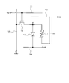
- Each pixel 104 is provided with a light emitting element.
- FIG. 2 shows an equivalent circuit of the pixel 104 according to the present embodiment.
- the pixel circuit shown in FIG. 2 includes a light emitting element 112, a transistor 110, and a photoconductive element 114. A point at which one end of these elements is connected in common is indicated as a node N1.
- a gate which is a control terminal is connected to the scanning signal line 118, and one end of a source / drain which is an input / output terminal is connected to the video signal line 120.
- the transistor 110 has a function of controlling the electrical connection between the video signal line 120 and the node N1.
- the photoconductive element 114 is substantially a two-terminal element, one end of which is connected to the first power supply line 122, and the other terminal of the circuit configuration is connected to the node N1.
- One end of the light emitting element 112 is connected to the second power supply line 124, and the other end is connected to the node N1.
- the scan signal line 118 receives a scan signal for controlling on / off of the transistor 110 from the scan signal line driver circuit 106.
- the scanning signal applies a gate voltage at which the transistor 110 is turned on at the timing when each pixel takes in a video signal from the video signal line 120 and a voltage at which the transistor 110 is turned off at other timings.
- a voltage based on the video signal is applied to the node N1.
- the light emitting element 112 emits light when the video signal voltage VSIG higher than the light emission threshold voltage VthOL is applied to the node N1.
- the light emitted from the light emitting element 112 becomes the emitted light of the pixel.
- a part of the light emitted from the light emitting element 112 becomes the irradiation light of the photoconductive element 114.
- the photoconductive element 114 has a characteristic that the resistivity in the bright state (the state in which light is irradiated) decreases with respect to the dark state.
- the photoconductive element 114 has a characteristic that the resistance value changes in accordance with the amount of light irradiated. In that sense, the photoconductive element 114 can also be regarded as a variable resistance element. The resistance value of the photoconductive element 114 may change depending on the irradiation light quantity (light intensity) of light.
- the photoconductive element 114 is formed using a semiconductor having a photoconductive effect between a pair of electrodes. Although a p-type or n-type semiconductor layer can be applied as the semiconductor layer, it is preferable to use a substantially intrinsic semiconductor film because it has a sufficiently high resistance value in the dark state.
- the photoconductive element 114 is a pn junction element using a p-type semiconductor and an n-type semiconductor, or a pin junction element in which a substantially intrinsic i-type semiconductor is provided between the p-type semiconductor and the n-type semiconductor It can also be realized by an element including such a semiconductor junction.
- the photoconductive element 114 has a resistance value to the extent that the effective current IOL0 emitted by the light emitting element 112 from the first power supply line 122 does not flow in the dark state. However, when the light emitting element 112 emits light, the resistance value of the photoconductive element 114 that has been irradiated with light decreases compared to the dark state. Then, when the resistance value of the photoconductive element 114 decreases, current flows from the first power supply line 122 to the light emitting element 112. When the effective current IEOL0 flows from the first power supply line 122 via the photoconductive element 114, the light emission of the light emitting element 112 is maintained. At this time, at least the voltage VD of the first power supply line 122 is higher than the potential VS of the second power supply line 124.
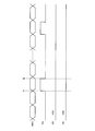
- FIG. 3 shows a timing chart for explaining the operation of the pixel circuit shown in FIG. This timing chart shows changes in the video signal voltage VSIG of the video signal line 120, the scanning signal voltage VG of the scanning signal line 118, the voltage VD of the first power supply line 122, and the voltage VS of the second power supply line 124. .
- the transistor 110 When the voltage VG of the scan signal line 118 becomes high (H level) at time t1, the transistor 110 is turned on. Then, the video signal line 120 and the node N1 become conductive, and the video signal voltage VSIG is applied to the node N1. At this time, when the video signal voltage VSIG is smaller than the light emission threshold voltage VthOL of the light emitting element 112, the light emitting element 112 does not emit light.
- the resistance value of the photoconductive element 114 in the dark state is sufficiently large, and an effective current for causing the light emitting element 112 to emit light from the first power supply line 122 does not flow.
- the transistor 110 When the voltage VG of the scanning signal line 118 becomes low (L level) at time t2, the transistor 110 is turned off, and the node N1 is disconnected from the video signal line 120. Therefore, the light emitting element 112 is maintained in the non-emission state.
- the voltage VD of the first power supply line 122 and the voltage VS of the second power supply line 124 are held at a constant potential. The relationship between the voltage VD of the first power supply line 122 and the voltage VS of the second power supply line 124 is maintained such that VD> VS.
- the effective current IOL0 flows in the light emitting element 112 to emit light.
- the light emission intensity of the light emitting element 112 changes in accordance with the effective current IOL0.
- a part of the light emitted from the light emitting element 112 is irradiated to the photoconductive element 114. Due to the light irradiation, the photoconductive element 114 has a lower resistance than in the dark state. That is, the photoconductive element 114 transitions from the high resistance state to the bottom resistance state by light irradiation.
- a large current IRV flows through the photoconductive element 114 as compared to the current in the dark state (dark current).
- current IRV is equal to or more than effective current IOL0
- the first power supply line A current flows from the light source 122 to the light emitting element 112 via the photoconductive element 114. At this time, the light emission of the light emitting element 112 is maintained.
- the resistance of the photoconductive element 114 is lowered thereafter and current flows from the first power supply line 122,
- the light emission state can be maintained. That is, light emission of the light emitting element 112 can be started and light emission can be maintained without depending on the threshold voltage of the transistor.
- FIG. 4 shows another example for explaining the operation of the pixel circuit shown in FIG. Here, the difference from FIG. 3 will be described.
- the voltage VD of the first power supply line 122 connected to the photoconductive element 114 changes from the high voltage VDD to a voltage VM1 lower than that.
- the low voltage VM1 is a voltage close to or less than the light emission threshold voltage VthOL of the light emitting element 112.
- the first power supply line 122 reaches the low voltage VM1
- the current supply to the light emitting element 112 is rapidly reduced. Therefore, the light emission of the light emitting element 112 is stopped.
- the resistance value of the photoconductive element 114 increases and returns to the dark state resistance value. That is, the photoconductive element 114 changes from the low resistance state to the high resistance state, and initialization is performed. If the voltage of the node N1 does not change between the time t3 and the time t4 and the light emitting element 112 does not emit light, the photoconductive element 114 is maintained with high resistance.
- the interval between time t3 and time t4 may be set as long as the time until the photoconductive element 114 returns to the resistance value in the dark state (high resistance) is secured, and if the above initialization can be practically performed. Good.
- the time from time t3 to time t4 may be secured until the photoexcitation carrier disappears.
- the video signal line 120 and the node N1 are conducted similarly to the case of FIG. become.
- the voltage VSIG is larger than the light emission threshold voltage VthOL of the light emitting element 112
- the light emitting element 112 emits light by the current from the video signal line 120.
- the transistor 110 is in the ON state.
- a signal current may flow from the video signal line 120 to the first power supply line 122 side.
- the voltage VD of the first power supply line 122 in the period from time t4 to time t5 may be set to a voltage VM2 higher than the low voltage VM1 and higher than the maximum value of the signal voltage VSIG.
- the period from time t4 to time t5 may be shortened as much as possible.
- the voltage VD of the first power supply line 122 may be changed from the low voltage VM1 to the high voltage VDD at time t4.
- the brightness of the light emitting element 112 is accurately controlled. It is possible to For example, when the light emitting element 112 emits light in one frame and moves to the next frame, if the resistance change of the photoconductive element 114 can not follow, unintended light emission may remain as an afterimage as a result. .
- the display device 100 controls the timing at which the light emitting element 112 starts light emission by the transistor 110 connected to the video signal line.
- the transistor 110 receives a video signal from the video signal line 120, and causes the light emitting element 112 to emit light based on the signal.
- the pixel 104 is provided with a photoconductive element 114 whose resistance is reduced by light irradiation of the light emitting element 112. When the light emitting element 112 emits light, an effective current flows from the power supply line to the light emitting element 112 through the photoconductive element 114 whose resistance is reduced thereafter, so that the light emitting element 112 can maintain the light emission.
- the light emitting element 112 emits light without being affected by the variation in threshold voltage of the transistor. It can be done.
- the driving transistor for controlling the current flowing through the light emitting element 112 with the drain current corresponding to the gate voltage is not provided.
- the transistor 110 controls on-off.
- the light emitting element 112 emits light at a luminance based on the video signal voltage VSIG, and when light emission is started, a current corresponding to the luminance flows from the first power supply line 122 through the photoconductive element 114. Accordingly, the light-emitting element 112 can emit light without being affected by variations in threshold voltage of the transistor, and can maintain the light-emitting state.
- IOL0 effective current
- the light emission intensity of the light emitting element 112 increases with time
- IRV ⁇ IOL0 the light emission intensity of the light emitting element 112 decreases with time.
- the video signal written to the pixel 104 is rewritten or rewritten in a fixed period. Therefore, the light emitting element 112 only needs to maintain light emission for a certain period, and a slight change in luminance can be regarded as within an allowable range.
- the pixel provided with the light emitting element only needs to have one transistor and a photoconductive element, and the number of elements required for one pixel can be reduced. That is, even without providing a driving transistor and a correction circuit for compensating for the threshold voltage of the driving transistor, which is conventionally required, a display device in which variations in luminance are prevented can be realized. Further, since there is no need for a drive transistor for controlling the current of the light emitting element, it is not necessary to strictly control the threshold voltage of the drive transistor, so that the process margin can be expanded in the manufacturing process of the display device.
- the operation can be stabilized by further adding a capacitive element to the pixel circuit shown in FIG.
- a capacitive element to the pixel circuit shown in FIG.
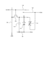
- FIG. 5 shows an example of connecting the capacitive element 116 to the node N1.
- One end of the capacitive element 116 is connected to the node N 1, and the other end is connected to the capacitive line 126.
- a constant voltage VC is applied to the capacitance line 126.
- the transistor 110 when the transistor 110 is turned on, the video signal line 120 and the node N1 become conductive, and the capacitor 116 is charged to the video signal voltage VSIG. After the transistor 110 is turned off, the light emitting element 112 can emit light by the video signal voltage VSIG charged in the capacitor 116.
- writing of a video signal to the pixel 104 and light emission can be controlled.
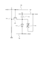
- FIG. 6 shows an example in which the other end of the capacitive element 116 is connected to the second power supply line 124.
- the pixel circuit illustrated in FIG. 6 can also cause the light emitting element 112 to emit light by the video signal voltage VSIG charged in the capacitive element 116.
- the other end of the capacitive element 116 is connected to the second power supply line 124, so the capacitive line 126 shown in FIG. 5 can be omitted.
- FIG. 7 shows an example in which the other end of the capacitive element 116 is connected to the first power supply line 122.
- the other end of the capacitive element 116 may be connected to the first power supply line 122 to omit the capacitance line.
- the light emission of the light emitting element 112 can be stabilized by adding the capacitor 116 to the pixel circuit.
- the light emission state of the light-emitting element can be stabilized.
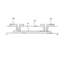
- FIG. 8A and 8B show an example of the photoconductive element 114.
- FIG. 8A is a plan view of the photoconductive element 114, and a cross-sectional structure corresponding to the line AB is shown in FIG. 8B.
- the photoconductive element 114 shown in FIGS. 8A and 8B has a structure in which a first electrode 136 and a second electrode 138 are provided on a photoconductive layer 134 having a photoelectric effect.
- the first electrode 136 and the second electrode 138 may be provided to contact at both ends of the photoconductive layer 134 with the insulating layer 140 interposed therebetween.
- the photoconductive layer 134 is preferably a semiconductor having a photoelectric effect, and for example, a semiconductor such as silicon (Si) or germanium (Ge) can be used. In addition, compound semiconductors such as CdTe, CuInSe 2 , and CuInS can be used.
- amorphous silicon is suitable as the photoconductive element 114 because the ratio of dark conductivity to photoconductivity is high.
- Amorphous silicon has a dark conductivity of 10 -10 S / cm or less, while the photoconductivity is expected to be 10 -6 S / cm or more, although it depends on the light irradiation intensity. Therefore, it works as a high resistor in the dark state and can be used as a low resistor at the time of light irradiation.
- amorphous silicon is characterized in that thin film formation is easy and the light absorption coefficient in the visible light band is higher than that of a crystalline silicon semiconductor. Therefore, the photoconductive element 114 can be provided in the pixel without largely changing the manufacturing process of the display device.
- FIG. 9A and 9B show another example of the photoconductive element 114.
- FIG. 9A is a plan view of the photoconductive element 114, and a cross-sectional structure corresponding to the line AB in FIG. 9A is shown in FIG. 9B.
- the photoconductive element 114 is provided with a first electrode 136 and a second electrode 138 at the top and the bottom so as to sandwich the photoconductive layer 134.
- one of the first electrode 136 and the second electrode 138 is a light-transmitting electrode, part of light emitted from the light emitting element 112 can be incident on the photoconductive layer 134.
- the photoconductive element 114 shown in FIGS. 9A and 9B various semiconductors having the photoelectric effect can be used as described above.
- amorphous silicon for example, is used as the photoconductive layer 134, visible light can be sufficiently absorbed by a film thickness of about 100 nm to 500 nm. Then, the area where the first electrode 136 and the second electrode 138 overlap the photoconductive layer 134 can be used as the effective area of the device, which is advantageous for miniaturization.
- the photoconductive layer 134 may be a semiconductor material of one conductivity type (p-type, i-type (intrinsic) or n-type). Further, with respect to the photoconductive layer 134, one side of the first electrode 136 and the second electrode 138 may be p-type, and the other side may be a pn junction as an n-type semiconductor. Furthermore, an i-type region may be provided between the p-type and n-type regions provided in the photoconductive layer 134.
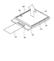
- FIG. 10 shows the configuration of the display device 100 according to the present embodiment in a perspective view.
- the second substrate 130 is disposed to face the first substrate 128, and is fixed by a sealing material.
- a pixel circuit is provided on the first substrate 128, and a pixel portion 102 is formed.
- the pixel portion 102 is sealed by the second substrate 130 so as not to be exposed to the air.
- the second substrate 130 may be a hard substrate such as a glass substrate, but may be an organic resin film substrate or an organic resin layer.
- a scan signal line driver circuit 106 and a video signal line driver circuit 108 are provided on the first substrate 128.
- the wiring substrate 132 is connected to the terminal portion of the first substrate 128.
- the wiring substrate 132 is also called a flexible circuit substrate (FPC substrate), and supplies an image signal and drive power from the external device into the display device 100.
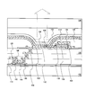
- FIG. 11 is a plan view of the pixel
- FIG. 12 shows a cross-sectional structure along the line C-D. The following description refers to these two figures.
- the pixel 104 includes a transistor 110, a light emitting element 112, and a photoconductive element 114.
- the semiconductor layer 142 in which a channel is formed and the gate electrode 146 are provided with the gate insulating layer 144 interposed therebetween.
- the transistor 110 has one input / output terminal connected to the video signal line 120 and the other input / output terminal connected to the source / drain electrodes 148 and 149.
- the source and drain electrodes 148 and 149 are electrically connected to the light emitting element 112.
- the semiconductor layer 142 which forms a channel of the transistor 110 can be formed using a silicon-based semiconductor such as amorphous silicon or polysilicon.
- the semiconductor layer 142 can be formed using an oxide semiconductor or an organic semiconductor.
- the transistor 110 is provided to be embedded in the interlayer insulating layer 150.
- the layer structure of the interlayer insulating layer 150 is optional.
- the interlayer insulating layer 150 can be configured by appropriately combining an inorganic insulating layer such as silicon oxide or silicon nitride, and an organic insulating layer such as a polyimide resin or an acrylic resin.
- the light emitting element 112 is provided on the interlayer insulating layer 150.
- the light emitting element 112 includes an individual pixel electrode 152 provided for each pixel, a light emitting layer 154 formed by containing a light emitting material, and a common pixel electrode 156 provided on the light emitting layer 154.
- the configuration of the light emitting layer 154 is optional, and can be formed using an organic electroluminescent material.
- the organic electroluminescent material a low molecular weight or high molecular weight material can be used.
- the light emitting layer 154 is a layer combining a guest material and a host material, and a hole injection layer or an electron injection layer sandwiching the layer, and a hole transport layer or an electron transport layer It may be configured to include etc.
- the light emitting element 112 can emit light in each band of red, green and blue depending on the selection of the light emitting material. Thus, each pixel can be divided into pixels corresponding to the respective colors.
- a structure in which layers containing light-emitting materials corresponding to the two colors B) and yellow (Y) may be stacked may be used.
- the light emitting element 112 is connected to the source and drain electrodes 148 and 149 which are input / output terminals of the transistor through the contact holes in which the individual pixel electrodes 152 are provided in the interlayer insulating layer 150.
- the individual pixel electrode 152 is applied with a voltage based on a video signal to be applied to the video signal line 120 through the transistor 110.
- the common pixel electrode 156 is continuously provided so as to be shared by a plurality of pixels, and a common potential is applied between the pixels.
- the individual pixel electrodes 152 are covered at their peripheral portions with the bank layer 158.
- the bank layer 158 opens the inner region excluding the periphery of the individual pixel electrode 152 and the region of the contact hole.
- the light emitting layer 154 and the common pixel electrode 156 are provided on the upper layer side of the bank layer 158.
- the light emitting layer 154 and the common pixel electrode 156 are stacked in a region where the individual pixel electrode 152 is opened by the bank layer 158.
- a region where the individual pixel electrode 152, the light emitting layer 154, and the common pixel electrode 156 overlap is a substantial light emitting region. That is, the stacked region functions as the light emitting element 112.
- a passivation layer 162 may be provided on the top surface of the common pixel electrode 156.
- the light emitting element 112 is configured to reflect light at the individual pixel electrode 152 and transmit light at the common pixel electrode 156 when light is emitted to the second substrate 130 side provided above the first substrate 128. Be done. Since light emitted from the light emitting layer 154 is emitted in all directions, the individual pixel electrode 152 is provided with a light reflecting surface in order to increase the amount of light emitted from the pixel 104. Alternatively, a light reflecting surface may be provided on the back side of the individual pixel electrode 152.
- the light emitting layer 154 is made of an organic electroluminescent material
- one of the individual pixel electrode 152 and the common pixel electrode 156 is an anode, and the other is a cathode.
- a conductive material having a high work function When the individual pixel electrode 152 side is an anode, it is considered preferable to use a conductive material having a high work function.
- a conductive material such as indium tin oxide (ITO) can be used. Since ITO or the like has translucency, in order to use the individual pixel electrode 152 as a light reflecting electrode, a metal layer such as silver or aluminum may be provided on the back surface.
- a material having a low work function such as lithium (Li) or magnesium (Mg) may be included.
- the common pixel electrode 156 may be formed by combining a layer containing the metal and a transparent conductive film such as ITO.
- the photoconductive element 114 is disposed at a position where part of the light emitted from the light emitting element 112 is irradiated. However, if the light emission surface of the pixel 104 is superimposed, the aperture ratio is reduced. Therefore, it is preferable to dispose the photoconductive element 114 around the light emitting element 112.
- FIG. 11 and 12 show an example in which the photoconductive element 114 is provided in a region overlapping with the bank layer 158.
- FIG. The bank layer 158 covers the peripheral portion of the first electrode 136 and has a characteristic of relieving a step.
- the photoconductive element 114 may be provided to be embedded in such a bank layer 158. By providing the photoconductive element 114 over the bank layer 158, the aperture ratio of the pixel can be prevented from being reduced.
- the photoconductive element 114 is a two-terminal element, one of which is connected to the first power supply line 122 and the other one of which is connected to the individual pixel electrode of the light emitting element 112.
- the photoconductive element 114 shown in FIGS. 11 and 12 has a structure in which a pair of electrodes are provided above and below the photoconductive layer 134.
- the electrode on the lower layer side of the photoconductive layer 134 corresponds to the first electrode 136
- the electrode on the upper layer side of the photoconductive layer 134 corresponds to the second electrode 138 in relation to FIG. Do.
- the first electrode 136 is formed by extending the individual pixel electrode 152 of the light emitting element 112 to the lower layer side of the bank layer 158.
- the connection structure between the light emitting element 112 and the photoconductive element 114 can be simplified.
- the photoconductive layer 134 is provided to have a region overlapping with the first electrode 136.
- the second electrode 138 is provided to cover one side of the photoconductive layer 134.
- the insulating layer 160 is provided on the photoconductive layer 134, and the second electrode 138 is connected to the photoconductive layer 134 at the opening. Note that the insulating layer 160 is not an essential component. However, since the second electrode 138 is connected by the photoconductive layer 134 through the opening provided on the upper surface portion to cover the side surface of the photoconductive layer 134, the first electrode 136 and the second electrode 138 are formed. It is possible to prevent a short circuit with the
- the light emitted from the light emitting layer 154 is emitted to the side of the second substrate 130, and a part is also emitted in an oblique direction with the bank layer 158.
- the bank layer 158 is formed using a translucent insulating material. When the bank layer 158 is translucent, part of the light emitted from the light emitting layer 154 passes through the bank layer 158 and enters the photoconductive layer 134 of the photoconductive element 114. When the photoconductive layer 134 is irradiated with light, photoexcited carriers are generated to lower the resistivity.
- the operation of the pixel circuit associated therewith is as described in FIG.
- the second electrode 138 which is one electrode of the photoconductive element 114 from the side surface to the top surface of the photoconductive layer 134, light incident from the adjacent pixel 104 can be blocked. By making the second electrode 138 double as a light shielding layer, malfunction of the photoconductive element 114 can be prevented.
- the photoconductive element 114 in the region overlapping with the bank layer 158, the aperture ratio of the pixel 104 can be prevented from being reduced. Further, since the photoconductive element 114 can be provided adjacent to the light emitting element 112, the photoresponsiveness and sensitivity can be improved.
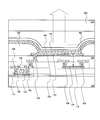
- FIG. 13 and 14 show another example of the pixel 104 according to the present embodiment.
- FIG. 13 is a plan view of the pixel
- FIG. 14 shows a cross-sectional structure along the line EF. In the following description, differences from FIGS. 11 and 12 will be described.
- the photoconductive element 114 is provided so as to be embedded in the interlayer insulating layer 150. Further, as shown in FIG. 13, the photoconductive element 114 is provided so as to overlap the individual pixel electrode 152.
- the photoconductive element 114 has an element structure similar to that described in FIGS. 9A and 9B, and a first electrode 136 and a second electrode 138 connected to the photoconductive layer 134 are juxtaposed. In this case, the second electrode 138 doubles as the first power supply line 122. Therefore, the photoconductive element 114 can be provided without increasing the layer structure of the interlayer insulating layer 150. By providing the photoconductive element 114 so as to be embedded in the interlayer insulating layer 150, the aperture ratio of the pixel can be prevented from being reduced.
- the photoconductive element 114 is disposed at a position where the light of the light emitting element 112 is irradiated.
- the photoconductive element 114 can be provided so as to partially overlap with the light emitting element 112.
- a light transmission window may be provided in the individual pixel electrode 152 so that light is emitted from the light emitting element 112.
- a reflection layer 153 formed of a metal material such as aluminum is provided, and an opening is provided in the reflection layer 153.
- Such a structure of the individual pixel electrode 152 allows the light of the light emitting layer 154 to be irradiated to the photoconductive layer 134.
- the photoconductive element 114 uses the first electrode 136 or the second electrode 138 as a light blocking layer in order to block light incident from adjacent pixels.
- the second electrode 138 is provided along the photoconductive layer 134 so that one surface of the photoconductive layer 134 is shielded from light. Since the second electrode 138 is formed of a metal material, it can be used as a light shielding layer.
- the distance between adjacent pixels can be narrowed. This can be said to be an advantageous configuration for achieving high definition of pixels.
- Electrode 100 display device 102: pixel portion 104: pixel 106: scanning signal line drive circuit 108: video signal line drive circuit 110: transistor 112: 112 Light emitting element 114: Photoconductive element 116: Capacitive element 118: Scanning signal line 120: Video signal line 122: First power supply line 124: Second Power line 126, capacitance line 128, first substrate 130, second substrate 132, wiring substrate 134, photoconductive layer 136, first Electrodes 138: second electrode 140: insulating layer 142: semiconductor layer 144: gate insulating layer 146: gate electrode 148, 149: source and drain Electrode, 150: interlayer insulating layer, 152: individual pixel electrode, 15 ... reflective layer, 154 ... light-emitting layer, 156 ... common pixel electrode, 158 ... bank layer, 160 ... insulating layer, 162 ... passivation layer
Landscapes
- Physics & Mathematics (AREA)
- Engineering & Computer Science (AREA)
- General Physics & Mathematics (AREA)
- Nonlinear Science (AREA)
- Theoretical Computer Science (AREA)
- Computer Hardware Design (AREA)
- Optics & Photonics (AREA)
- Chemical & Material Sciences (AREA)
- Life Sciences & Earth Sciences (AREA)
- Inorganic Chemistry (AREA)
- Sustainable Development (AREA)
- Mathematical Physics (AREA)
- Crystallography & Structural Chemistry (AREA)
- Electroluminescent Light Sources (AREA)
- Control Of Indicators Other Than Cathode Ray Tubes (AREA)
- Control Of El Displays (AREA)
Abstract
画素回路を簡略化しつつ発光素子の輝度ばらつきの抑制を図ることのできる表示装置を提供することを目的の一つとする。ゲートが走査信号線と接続され、入出力端子の一方の端子が映像信号線と接続されるトランジスタと、一端がトランジスタの入出力端子の他方の端子と接続され、他端が第1の電源線と接続される光導電素子と、一端がトランジスタの入出力端子の他方の端子と接続され、他端が第2の電源線と接続される発光素子と、を有する表示装置が提供される。
Description
本発明は、表示装置の画素の構造及び画素回路の構成、並びに表示装置駆動方法に関する。
平板型表示装置として、有機エレクトロルミネセンス材料を含んで発光層が形成される発光素子で画素を構成した表示装置が開発されている。この表示装置は、発光素子が発光するタイミング及び発光輝度を制御する回路(以下、「画素回路」ともいう。)が表示部に設けられている。
画素回路は、映像信号を取り込むスイッチング素子と、発光素子の電流を制御する駆動トランジスタを基本構成として含んでいる。駆動トランジスタは、ゲート電圧が映像信号によって制御され、ゲート電圧に基づくドレイン電流が発光素子に流れることで発光輝度が制御される。駆動トランジスタは、半導体薄膜によって形成される薄膜トランジスタによって実現されている。画素回路は、基本的に、各画素の駆動トランジスタの特性が一様であることを前提としている。駆動トランジスタのドレイン電流がゲート電圧によって一様に定まれば、発光素子の輝度は均一化され、それによって正確な階調表示を実現される。
しかし、薄膜トランジスタのしきい値電圧は、製造プロセス上の制御が困難であり、画素ごとにばらついてしまうのが通常である。駆動トランジスタのしきい値電圧の変動は、ドレイン電流に影響を与え、結果として発光素子の輝度をばらつかせる原因となる。表示装置において、各画素の輝度ばらつきは、表示むらとして視認される。このため、表示装置の画素回路には、各画素に設けられる駆動トランジスタのしきい値電圧を補償する回路を必要としている(例えば、特許文献1参照)。
発光素子で画素を構成した表示装置のもう一つの問題は、発光素子自体の特性ばらつきと、輝度劣化である。発光素子は同一電流を供給しても発光輝度がばらつき、また発光輝度が経時的に低下するという問題を有している。発光素子の輝度ばらつき及び輝度劣化による視認性の低下を防ぐために、画素に光電変換素子を設けた表示装置が開示されている(特許文献2及び3参照)。この表示装置は、発光素子の放射光の一部を光電変換素子が受光して、発光輝度に応じて発光素子の駆動電流を制御するフィードバック型の画素回路が設けられている。
特許文献1に開示される表示装置によれば、しきい値電圧補償回路を構成するために、一つの画素に6個のトランジスタと1つの容量素子が必要とされている。この画素回路は、一つの画素内に多くの素子を設ける必要があるため、一画素を形成するために必要な面積が大きくなってしまうことが問題となる。
また、特許文献2及び3に開示される表示装置によれば、発光素子の駆動電流はトランジスタによって制御されるため、当該トランジスタのしきい値電圧を補償するにはしきい値電圧補償回路を画素内に設ける必要がある。
このように発光素子を用いた従来の表示装置によれば、発光素子の発光輝度を安定化させ画質の向上を図るために、一画素当たり多くの素子を設ける必要があり、高精細化を困難にしている。
このような問題に鑑み、本発明の一実施形態は、画素回路を簡略化しつつ発光素子の輝度ばらつきの抑制を図ることのできる表示装置を提供することを目的の一つとする。
本発明の一実施形態によれば、ゲートが走査信号線と接続され、入出力端子の一方の端子が映像信号線と接続されるトランジスタと、一端がトランジスタの入出力端子の他方の端子と接続され、他端が第1の電源線と接続される光導電素子と、一端がトランジスタの入出力端子の他方の端子と接続され、他端が第2の電源線と接続される発光素子と、を有する表示装置が提供される。
本発明の一実施形態によれば、ゲートが走査信号線と接続され、ソース及びドレインの一方が映像信号線と接続されるトランジスタと、個別画素電極と、個別画素電極上の発光層と、発光層上の共通画素電極とが積層された発光素子と、第1の電極と第2の電極とが、それぞれ光導電層に接続される光導電素子と、を有し、個別画素電極はトランジスタのソース及びドレインの他方と接続され、第1の電極は個別画素電極と接続され、第2の電極は電源線と接続されている表示装置が提供される。
本発明の一実施形態によれば、ソース及びドレインの一端が映像信号線に接続されたトランジスタを時刻t1でオンにすることで、ソース及びドレインの他端であるノードN1に映像信号電圧を与え、ノードN1の電圧に基づいて、一端が前記ノードN1に接続された発光素子を発光させ、発光素子の発光により、電源線とノードN1との間に接続された光導電素子の抵抗を高抵抗状態から低抵抗状態に遷移させ、時刻t2でトランジスタがオフとなった後も、電源線から発光素子に発光状態を維持する有効電流を供給する表示装置の駆動方法が提供される。
以下、本発明の実施の形態を、図面等を参照しながら説明する。但し、本発明は多くの異なる態様で実施することが可能であり、以下に例示する実施の形態の記載内容に限定して解釈されるものではない。また、図面は説明をより明確にするため、実際の態様に比べ、各部の幅、厚さ、形状等について模式的に表される場合があるが、あくまで一例であって、本発明の解釈を限定するものではない。また、本明細書と各図において、既出の図に関して前述したものと同様の要素には、同一の符号を付して、詳細な説明を適宜省略することがある。
本明細書において、ある部材又は領域が、他の部材又は領域の「上に(又は下に)」あるとする場合、特段の限定がない限り、これは他の部材又は領域の直上(又は直下)にある場合のみでなく、他の部材又は領域の上方(又は下方)にある場合を含み、すなわち、他の部材又は領域の上方(又は下方)において間に別の構成要素が含まれている場合も含む。
<表示装置の構成>
図1は本実施形態に係る表示装置100の構成を示す。表示装置100は、表示画面を形成する画素部102、画素部102に走査信号を出力する走査信号線駆動回路106、画素部102に映像信号を出力する映像信号線駆動回路108を含んで構成されている。画素部102は、複数の画素104が配列され画素回路が形成されている。それぞれの画素104には発光素子が設けられている。
図1は本実施形態に係る表示装置100の構成を示す。表示装置100は、表示画面を形成する画素部102、画素部102に走査信号を出力する走査信号線駆動回路106、画素部102に映像信号を出力する映像信号線駆動回路108を含んで構成されている。画素部102は、複数の画素104が配列され画素回路が形成されている。それぞれの画素104には発光素子が設けられている。
図2は、本実施形態に係る画素104の等価回路を示す。図2で示す画素回路は、発光素子112、トランジスタ110及び光導電素子114を含んで構成されている。そして、これらの素子の一端が共通に接続される点をノードN1と表示している。
トランジスタ110は、制御端子であるゲートが走査信号線118と接続され、入出力端子であるソース・ドレインの一端が映像信号線120と接続されている。トランジスタ110は、映像信号線120とノードN1との電気的接続を制御する機能を有している。光導電素子114は実質的に2端子素子であり、一端が第1の電源線122と接続され、回路構成上もう一方の端子はノードN1と接続されている。発光素子112は、一端が第2の電源線124と接続され、他端はノードN1と接続されている。
走査信号線118は、走査信号線駆動回路106からトランジスタ110のオン-オフを制御する走査信号が入力される。走査信号は、各画素が映像信号線120から映像信号を取り込むタイミングでトランジスタ110がオンとなるゲート電圧を与え、それ以外のタイミングでオフとなる電圧を与える。トランジスタ110がオンになると、映像信号に基づく電圧がノードN1に与えられる。
発光素子112は、ノードN1に発光しきい値電圧VthOL以上の映像信号電圧VSIGが与えられると発光する。発光素子112から放出される光は画素の出射光となる。また、発光素子112から放出される光の一部は、光導電素子114の照射光となる。光導電素子114は、暗状態に対し明状態(光が照射された状態)の抵抗率が低下する特性を有している。また、光導電素子114は、光の照射光量に応じて抵抗値が変化する特性を有している。その意味で、光導電素子114は抵抗可変素子とみなすこともできる。光導電素子114の抵抗値は、光の照射光量(光強度)によって変化し得る。
光導電素子114は、一対の電極間に光導電効果を有する半導体を用いて形成される。半導体層としては、p型又はn型の半導体層を適用し得るが、暗状態において十分高い抵抗値を有するために実質的に真性の半導体膜を用いることが好ましい。また、光導電素子114は、p型半導体とn型半導体を用いたpn接合素子、またはp型半導体とn型半導体との間に実質的に真性なi型半導体を設けたpin接合素子、もしくはそのような半導体接合を含む素子によって実現することもできる。
光導電素子114は、暗状態で第1の電源線122から発光素子112が発光する有効電流IOL0が流れない程度の抵抗値を有している。しかし、発光素子112の発光することで光照射を受けた光導電素子114は、暗状態に比べ抵抗値が低下する。そして、光導電素子114の抵抗値が低下すると、第1の電源線122から発光素子112へ電流が流れる。第1の電源線122から光導電素子114を介して有効電流IEOL0が流れると、発光素子112の発光が維持される。なお、このとき、少なくとも第1の電源線122の電圧VDは第2の電源線124の電位VSより高電位であるものとする。
<動作方式>
図3は、図2に示す画素回路の動作を説明するタイミングチャートを示す。このタイミングチャートは、映像信号線120の映像信号電圧VSIG、走査信号線118の走査信号電圧VG、第1の電源線122の電圧VD、第2の電源線124の電圧VSの変化を示している。
図3は、図2に示す画素回路の動作を説明するタイミングチャートを示す。このタイミングチャートは、映像信号線120の映像信号電圧VSIG、走査信号線118の走査信号電圧VG、第1の電源線122の電圧VD、第2の電源線124の電圧VSの変化を示している。
時刻t1で走査信号線118の電圧VGが高電圧(Hレベル)になると、トランジスタ110がオン状態となる。そうすると、映像信号線120とノードN1が導通状態となり、ノードN1に映像信号電圧VSIGが与えられる。このとき、映像信号電圧VSIGが発光素子112の発光しきい値電圧VthOLよりも小さい場合、発光素子112は発光しない。光導電素子114の暗状態の抵抗値は十分大きく、第1の電源線122から発光素子112を発光させるだけの有効電流は流れない。
時刻t2で走査信号線118の電圧VGが低電圧(Lレベル)になると、トランジスタ110がオフ状態となり、ノードN1は映像信号線120と遮断された状態となる。そのため、発光素子112は発光しない状態が維持される。このとき、第1の電源線122の電圧VDと第2の電源線124の電圧VSは一定電位に保持されている。なお、第1の電源線122の電圧VDと第2の電源線124の電圧VSの関係は、VD>VSが維持されている。
一方、時刻t1で、ノードN1の電圧VSIGが発光素子112の発光しきい値電圧VthOLよりも大きい場合、発光素子112には有効電流IOL0が流れ発光する。発光素子112の発光強度は、有効電流IOL0に応じて変化する。発光素子112から出射された光の一部は光導電素子114に照射される。光導電素子114は、光照射により暗状態に比べ抵抗値が低下する。すなわち、光導電素子114は光照射により高抵抗状態から底抵抗状態に遷移する。それにより、光導電素子114には暗状態の電流(暗電流)に比べて大きな電流IRVが流れる。この場合、時刻t2でトランジスタ110がオフとなりノードN1が映像信号線120と遮断された後も、電流IRVが有効電流IOL0と同じか、それよりも十分な電流であれば、第1の電源線122から光導電素子114を介して発光素子112に電流が流れる。このとき発光素子112の発光は維持される。
このように、図3で示す画素回路の動作によれば、映像信号により発光素子112を発光させれば、その後は光導電素子114が低抵抗化して第1の電源線122から電流が流れ込み、発光状態を維持することができる。すなわち、トランジスタのしきい値電圧に依存せず、発光素子112の発光を開始させ、発光を維持することができる。
図4は、図2で示す画素回路の動作を説明する他の一例を示す。ここでは、図3との相違について説明する。
時刻t3において、光導電素子114に接続する第1の電源線122の電圧VDが高電圧VDDから、それよりも低い電圧VM1に変化している。ここで、低電圧VM1は発光素子112の発光しきい値電圧VthOLに近い電圧かそれ以下の電圧であるものとする。
第1の電源線122が低電圧VM1になると、発光素子112への電流供給は急速に低下する。そのため発光素子112の発光は停止する。発光素子112の発光が停止すると、光導電素子114の抵抗値は増加し暗状態の抵抗値に戻る。すなわち、光導電素子114は低抵抗状態から高抵抗状態に変化し、初期化がなされたことになる。時刻t3から時刻t4の間で、ノードN1の電圧が変化せず発光素子112が発光しなければ、光導電素子114は高抵抗のまま保持される。時刻t3と時刻t4の間隔は、光導電素子114が暗状態の抵抗値(高抵抗)に戻るまでの時間が確保されていればよく、実用的に上記の初期化ができる時間設定にすればよい。
例えば、光導電素子114が半導体層の光導電効果による抵抗変化を利用している場合、時刻t3から時刻t4の時間は、光励起キャリアが消滅するまので時間が確保されていればよい。
時刻t4で走査信号線118の電圧VGが高電圧(Hレベル)となり、トランジスタ110がオンになると、図2の場合と同様に映像信号線120とノードN1が導通し、ノードN1が信号電圧VSIGになる。電圧VSIGが発光素子112の発光しきい値電圧VthOLよりも大きい場合は、映像信号線120からの電流により発光素子112が発光する。
このとき、第1の電源線122の電圧VDは低電圧VM1の状態にあるので、発光素子112が発光することにより光導電素子114の抵抗値が低下すると、トランジスタ110はオン状態にあるので、映像信号線120から信号電流が第1の電源線122側に流れ込んでしまう可能性がある。これを回避するには、時刻t4から時刻t5の期間における第1の電源線122の電圧VDを低電圧VM1よりも高く、かつ信号電圧VSIGの最大値よりも高い電圧VM2にすればよい。または、時刻t4から時刻t5の期間を可能な限り短くすればよい。あるいは、時刻t4で第1の電源線122の電圧VDを低電圧VM1から高電圧VDDにしてもよい。
時刻t5において、第1の電源線122の電圧VDを高電圧VDDにすると、図2の場合と同様に、第1の電源線122から発光素子112へ電流が流れる。時刻t6で、走査信号線118の電圧が低電圧(Lレベル)に変化すると、トランジスタ110がオフとなり、映像信号線120とノードN1は電気的に遮断される。しかし、第1の電源線122から光導電素子114を介して発光素子112へ電流の供給は続くので、発光素子112は発光を維持することができる。
図4で示す画素回路の動作によれば、光導電素子114の抵抗変化が、発光素子112の点滅(発光と非発光)に対して十分追従できない場合でも、発光素子112の輝度を正確に制御することが可能となる。例えば、発光素子112がある1フレームで発光している状態から次のフレームに移る際、光導電素子114の抵抗変化が追従できないと、結果として意図しない発光が残像のように残る可能性がある。また、同じ原因から、ある1フレームで発光素子112が発光するときに、前のフレームの明暗状態が影響して光導電素子114の抵抗値が追従できないでいると、映像信号電圧に応じた輝度で正確に発光できないという不具合の発生が起こり得る。しかしながら、図4で示すように、発光素子112の発光を強制的に停止させ、光導電素子114を初期化する期間を設けることで、このような不具合を回避することができる。
本発明の一実施形態に係る表示装置100は、発光素子112が発光を開始するタイミングを、映像信号線に接続されたトランジスタ110によって制御する。トランジスタ110は映像信号線120から映像信号を取り込み、当該信号に基づいて発光素子112を発光させる。画素104には発光素子112の光照射によって低抵抗化する光導電素子114が設けられている。発光素子112が発光すると、以降は低抵抗化した光導電素子114を介して電源線から有効電流が発光素子112に流れ込むので、発光素子112は発光を維持することができる。このように、発光素子112の発光時の電流を、実質的に抵抗素子とみなせる光導電素子114により制御することで、トランジスタのしきい値電圧のばらつきの影響を受けずに発光素子112を発光させることができる。
本実施形態に係る画素回路によれば、発光素子112に流れる電流をゲート電圧に応じたドレイン電流で制御する駆動トランジスタは設けられていない。トランジスタ110はオン-オフを制御している。発光素子112は映像信号電圧VSIGに基づく輝度で発光し、発光が開始すればその輝度に応じた電流が光導電素子114を介して第1の電源線122から流れ込む。したがって、発光素子112はトランジスタのしきい値電圧のばらつきの影響を受けずに発光し、発光状態を維持することができる。
このとき、第1の電源線122から発光素子112に流れ込む電流IRVが有効電流IOL0と等しい(IRV=IOL0)ことが好ましいが、これは絶対的な要請事項とはならない。例えば、IRV>IOL0の場合は発光素子112の発光強度は時間とともに増加し、IRV<IOL0の場合は発光素子112の発光強度は時間とともに減少する。しかしながら、表示装置100において、画素104に書き込まれる映像信号は、一定の期間で書き換えられ、あるいは再書き込みされる。そのため、発光素子112は、一定期間だけ発光を維持できればよく、多少の輝度変化は許容範囲内とみなすことができる。
本実施形態によれば、発光素子が設けられた画素は、1つのトランジスタと光導電素子があればよく、一つの画素に必要な素子の数を削減することができる。すなわち、従来必要とされた、駆動トランジスタや、当該駆動トランジスタのしきい値電圧を補償する補正回路を設けなくても、輝度のばらつきを防いだ表示装置を実現することができる。また、発光素子の電流を制御する駆動トランジスタを必要としないので、当該駆動トランジスタのしきい値電圧を厳密に管理する必要がないので、表示装置の製造段階においてプロセスマージンを広げることができる。
<画素回路の変形例>
本実施形態において、図2で示す画素回路に、さらに容量素子を付加することで、動作の安定化を図ることができる。以下、図5、図6、図7を参照して、その一例を説明する。
本実施形態において、図2で示す画素回路に、さらに容量素子を付加することで、動作の安定化を図ることができる。以下、図5、図6、図7を参照して、その一例を説明する。
図5は、ノードN1に容量素子116を接続する一例を示す。容量素子116の一端はノードN1と接続され、他端は容量線126と接続されている。容量線126には一定の電圧VCが印加されている。この画素回路では、トランジスタ110がオンになると映像信号線120とノードN1が導通し、容量素子116は映像信号電圧VSIGに充電される。トランジスタ110がオフになった後、容量素子116に充電された映像信号電圧VSIGによって発光素子112を発光させることができる。このとき、容量線126の電位を制御することにより、画素104に対する映像信号の書き込みと発光を制御することができる。
図6は、容量素子116の他端を第2の電源線124に接続した一例を示す。図6に示す画素回路も、容量素子116に充電された映像信号電圧VSIGにより、発光素子112を発光させることができる。容量素子116の他端は第2の電源線124に接続されているので、図5で示す容量線126を省略することができる。
図7は、容量素子116の他端を第1の電源線122に接続する例を示す。図3で示すように、第1の電源線122の電圧を一定に保つ場合には容量素子116の他端を第1の電源線122に接続して、容量線を省略するようにしてもよい。いずれにしても、画素回路に容量素子116を付加することにより、発光素子112の発光を安定化させることができる。
図5、図6、図7で示すように、画素回路に容量素子を追加することで、発光素子の発光状態を安定化させることができる。
<光導電素子>
図8A及び図8Bは、光導電素子114の一例を示す。図8Aは光導電素子114の平面図であり、同図A-B線に対応した断面構造を図8Bに示す。図8A及び図8Bで示す光導電素子114は、光電効果を有する光導電層134に第1の電極136及び第2の電極138が設けられた構造を有している。第1の電極136及び第2の電極138は絶縁層140を挟んで光導電層134の両端でコンタクトするように設けられていてもよい。光導電層134は光電効果を有する半導体を用いるのが好ましく、例えば、シリコン(Si)、ゲルマニウム(Ge)などの半導体を用いることができる。また、CdTe、CuInSe2、CuInSなどの化合物半導体を用いることができる。
図8A及び図8Bは、光導電素子114の一例を示す。図8Aは光導電素子114の平面図であり、同図A-B線に対応した断面構造を図8Bに示す。図8A及び図8Bで示す光導電素子114は、光電効果を有する光導電層134に第1の電極136及び第2の電極138が設けられた構造を有している。第1の電極136及び第2の電極138は絶縁層140を挟んで光導電層134の両端でコンタクトするように設けられていてもよい。光導電層134は光電効果を有する半導体を用いるのが好ましく、例えば、シリコン(Si)、ゲルマニウム(Ge)などの半導体を用いることができる。また、CdTe、CuInSe2、CuInSなどの化合物半導体を用いることができる。
光導電素子114に用いる半導体として、アモルファスシリコンは、暗伝導度と光伝導度の比率が高いため、光導電素子114として好適である。アモルファスシリコンは、暗伝導度が10-10S/cm以下であるのに対し、光伝導度は光照射強度によるものの、10-6S/cm以上が見込まれる。そのため暗状態では高抵抗体として働き、光照射時には低抵抗体として用いることができる。また、アモルファスシリコンは、薄膜形成が容易であり、可視光帯域における光吸収係数が結晶シリコン半導体よりも高いという特徴がある。そのため、表示装置の製造プロセスを大幅に変更することなく、画素内に光導電素子114を設けることができる。
図9A及び図9Bは、光導電素子114の他の一例を示す。図9Aは光導電素子114の平面図であり、同図A-B線に対応した断面構造を図9Bに示す。この光導電素子114は、光導電層134を挟むように上下に第1の電極136と第2の電極138とが設けられている。この場合、第1の電極136及び第2の電極138の一方を透光性の電極とすれば、発光素子112から放射される光の一部を光導電層134に入射させることができる。
図9A及び図9Bで示す光導電素子114においても、前述と同様に光電効果を有する各種半導体を用いることができる。光導電層134として、例えばアモルファスシリコンを用いれば、100nmから500nm程度の膜厚により可視光を十分に吸収することができる。そして、第1の電極136及び第2の電極138が光導電層134と重なる領域が素子の有効面積として利用できるので、微細化に有利である。
図8A及び図8B、並びに図9A及び図9Bで示す光導電素子114において、光導電層134は一導電型(p型、i型(真性)又はn型)の半導体材料であればよい。また、光導電層134に対し、第1の電極136及び第2の電極138の一方の側をp型とし、他方の側をn型の半導体としてpn接合を設けるようにしてもよい。さらに、光導電層134に設けられたp型とn型の領域の間にi型領域を設けてもよい。光導電素子114をpn接合又はpin接合を設けたダイオード型の素子とすることで、光で励起されたキャリアは内部電界によりドリフトされるので、光応答速度を高めることができる。
<画素の構造>
図10は、本実施形態に係る表示装置100の構成を斜視図で示す。表示装置100は、第1の基板128に対し第2の基板130が対向配置され、シール材で固定されている。第1の基板128には画素回路が設けられ画素部102が形成されている。画素部102は第2の基板130によって大気に晒されないように封止されている。第2の基板130は、ガラス基板のような硬質基板であってもよいが、有機樹脂フィルム基板又は有機樹脂層であってもよい。
図10は、本実施形態に係る表示装置100の構成を斜視図で示す。表示装置100は、第1の基板128に対し第2の基板130が対向配置され、シール材で固定されている。第1の基板128には画素回路が設けられ画素部102が形成されている。画素部102は第2の基板130によって大気に晒されないように封止されている。第2の基板130は、ガラス基板のような硬質基板であってもよいが、有機樹脂フィルム基板又は有機樹脂層であってもよい。
また、第1の基板128には、走査信号線駆動回路106、映像信号線駆動回路108が設けられている。第1の基板128の端子部には配線基板132が接続されている。配線基板132はフレキシブル回路基板(FPC基板)とも呼ばれ、外部機器から映像信号、駆動電力を表示装置100内に供給している。
画素部102に設けられる画素104の構成を図11及び図12を参照して説明する。図11は画素の平面図であり、同図C-D線に沿った断面構造を図12に示す。以下の説明ではこの両図を参照する。
画素104は、トランジスタ110、発光素子112、光導電素子114を含んで構成されている。トランジスタ110は、チャネルが形成される半導体層142とゲート電極146とがゲート絶縁層144を介して設けられている。トランジスタ110は、一方の入出力端子が映像信号線120と接続され、他方の入出力端子がソース・ドレイン電極148、149と接続されている。ソース・ドレイン電極148、149は発光素子112と電気的に接続されている。トランジスタ110のチャネルを形成する半導体層142は、アモルファスシリコン及びポリシリコンなどのシリコン系半導体で形成することができる。また、半導体層142を、酸化物半導体、有機半導体を用いて形成することができる。
トランジスタ110は層間絶縁層150に埋設されるように設けられている。層間絶縁層150の層構造は任意である。層間絶縁層150は、酸化シリコン、窒化シリコンなどの無機絶縁層、およびポリイミド樹脂、アクリル樹脂などの有機絶縁層を適宜組み合わせて構成することができる。
発光素子112は、この層間絶縁層150の上に設けられている。発光素子112は、画素ごとに設けられる個別画素電極152と、発光材料を含んで形成される発光層154及び発光層154の上に設けられる共通画素電極156を含んで構成されている。発光層154の構成は任意であり、有機エレクトロルミネセンス材料を用いて形成することができる。
有機エレクトロルミネセンス材料としては、低分子系又は高分子系の材料を用いることができる。低分子系の有機材料を用いる場合、発光層154はゲスト材料とホスト材料を組み合わせた層の加え、当該層を挟むように正孔注入層や電子注入層、さらに正孔輸送層や電子輸送層等含んで構成されていてもよい。発光素子112は、発光材料の選択により、赤色、緑色及び青色の各帯域の光を発光することができる。それによって、各画素は、各色に対応した画素に作り分けることができる。また、発光素子112を白色発光とするには、有機EL層154に赤色(R)、緑色(G)、青色(B)の各色に対応する発光材料を含む層を積層する構造、または青色(B)と黄色(Y)の2色に対応する発光材料を含む層を積層した構造としてもよい。
発光素子112は、個別画素電極152が層間絶縁層150に設けられたコンタクトホールを介してトランジスタの入出力端子であるソース・ドレイン電極148、149と接続されている。個別画素電極152は、トランジスタ110を介して映像信号線120に当たられる映像信号に基づく電圧が印加される。また、共通画素電極156は、複数の画素間で共有するように連続して設けられ、画素間に共通する電位が与えられる。
また、個別画素電極152は、周縁部がバンク層158で覆われている。別言すれば、バンク層158は、個別画素電極152の周縁部及びコンタクトホールの領域を除く内側領域を開口している。発光層154及び共通画素電極156は、バンク層158の上層側に設けられている。発光層154及び共通画素電極156は、個別画素電極152がバンク層158で開口される領域において積層されている。個別画素電極152、発光層154及び共通画素電極156が重なる領域が実質的な発光領域となる。すなわち、当該積層領域が発光素子112として機能する領域となる。共通画素電極156の上面にはパッシベーション層162が設けられていてもよい。
発光素子112は、第1の基板128の上方に設けられる第2の基板130側に光を出射させる場合、個別画素電極152で光を反射させ、共通画素電極156で光を透過するように構成される。発光層154で発光した光は全方向に放射されるので、画素104の出射光量を高めるために個別画素電極152に光反射面を設ける。または個別画素電極152の背面側に光反射面を設けるようにしてもよい。発光層154を有機エレクトロルミネセンス材料により構成するときは、個別画素電極152及び共通画素電極156の一方を陽極とし、他方を陰極とする。個別画素電極152側を陽極とする場合、仕事関数の高い導電材料を用いることが好ましいとされている。該当する電極材料として、酸化インジウム・スズ(ITO)等の導電性材料を用いることができる。ITOなどは透光性を有するため、個別画素電極152を光反射電極とするには、背面に銀、アルミニウムなどの金属層を設けるようにしてもよい。一方、共通画素電極156を陰極とするには、リチウム(Li)、マグネシウム(Mg)等の仕事関数の低い材料を含んで構成するようにしてもよい。例えば、当該金属を含む層と、ITO等の透明導電膜を組み合わせて共通画素電極156としてもよい。
光導電素子114は、発光素子112から放射される光の一部が照射される位置に配置される。もっとも、画素104の光出射面に重ねてしまうと、開口率が低下してしまう。そのため、光導電素子114は発光素子112の周辺部に配置することが好ましい配置となる。
図11及び図12は、光導電素子114をバンク層158と重なる領域に設ける一例を示す。バンク層158は第1の電極136の周縁部を被覆して段差を緩和する特性を有している。光導電素子114は、このようなバンク層158で埋設されるように設けられてもよい。光導電素子114をバンク層158に重ねて設けることで、画素の開口率を低下させないようにすることができる。
図2で示すように、光導電素子114は2端子素子であり、一方が第1の電源線122に接続され、他方が発光素子112の個別画素電極と接続される。図11及び図12で示す光導電素子114は、光導電層134の上下に一対の電極を設けた構造を有している。ここでは、便宜上、図10との関係において、光導電層134の下層側にある電極を第1の電極136、光導電層134の上層側にある電極を第2の電極138に相当するものとする。第1の電極136は、発光素子112の個別画素電極152をバンク層158の下層側にまで延長することによって形成されている。このように、個別画素電極152が第1の電極136を兼ねるようにすることで、発光素子112と光導電素子114との接続構造を簡略化することができる。
光導電層134は第1の電極136と重なる領域を有するように設けられている。第2の電極138は、光導電層134の一方の面を覆うように設けられている。本実施形態では、光導電層134の上に絶縁層160を設け、開口部で第2の電極138が光導電層134と接続されている。なお、絶縁層160は必須の構成ではない。しかし、光導電層134の側面部を覆い上面部に設けた開口部で第2の電極138が光導電層134で接続されるようにしたことで、第1の電極136と第2の電極138との短絡を防止することができる。
発光層154から放射される光は、第2の基板130側に出射される他、一部はバンク層158のある斜め方向にも出射される。バンク層158は透光性を有する絶縁材料を用いて形成されている。バンク層158が透光性であると、発光層154から放射された光の一部はバンク層158を透過して光導電素子114の光導電層134に入射する。光導電層134は光が照射されることにより光励起キャリアが発生して抵抗率が低下する。それに伴う画素回路の動作は図2で説明したとおりである。
光導電素子114の一方の電極である第2の電極138を光導電層134の側面から上面に設けることで、隣接する画素104から入射する光を遮光することができる。第2の電極138が遮光層を兼ねるようにすることで、光導電素子114の誤動作を防止することができる。
図11及び図12で示す画素104によれば、光導電素子114をバンク層158と重なる領域に設けることで、画素104の開口率を低下させないようにすることができる。また、発光素子112に隣接して光導電素子114を設けることができるので、光応答性及び感度を向上させることができる。
図13及び図14は、本実施形態に係る画素104の他の一例を示す。図13は画素の平面図であり、同図E-F線に沿った断面構造を図14に示す。以下の説明では、図11及び図12との相違部分について説明する。
図14で示すように、光導電素子114は層間絶縁層150に埋設されるように設けられている。また、図13で示すように、光導電素子114は、個別画素電極152と重なるように設けられている。光導電素子114は、図9A及び図9Bで説明したものと同様の素子構造を有し、光導電層134と接続する第1の電極136と第2の電極138が並置されている。この場合、第2の電極138は、第1の電源線122を兼ねている。そのため、層間絶縁層150の層構造を増加させないでも光導電素子114を設けることができる。光導電素子114は層間絶縁層150に埋設されるように設けることで、画素の開口率を低下させないようにすることができる。
この場合も光導電素子114は、発光素子112の光が照射される位置に配置される。例えば、光導電素子114は、発光素子112と一部が重なるように設けることができる。なお、発光素子112から光が照射されるように、個別画素電極152に光透過窓を設けておいてもよい。例えば、光反射電極として形成される個別画素電極152の下層側に、アルミニウム等の金属材料で形成される反射層153を設け、当該反射層153に開口部を設けておく。このような個別画素電極152の構造により、発光層154の光が、光導電層134に光が照射されるようにすることができる。
光導電素子114は、隣接する画素から入射する光を遮光するために、第1の電極136又は第2の電極138を遮光層として用いる。図13では、光導電層134の一方の面が遮光されるように、第2の電極138が光導電層134に沿って設けられている。第2の電極138は金属材料で形成されるので、遮光層として用いることができる。
図13及び図14で示す画素104の構造によれば、隣接する画素同士の間隔を狭めることができる。それにより、画素の高精細化を図る上で有利な構成ということができる。
100・・・表示装置、102・・・画素部、104・・・画素、106・・・走査信号線駆動回路、108・・・映像信号線駆動回路、110・・・トランジスタ、112・・・発光素子、114・・・光導電素子、116・・・容量素子、118・・・走査信号線、120・・・映像信号線、122・・・第1の電源線、124・・・第2の電源線、126・・・容量線、128・・・第1の基板、130・・・第2の基板、132・・・配線基板、134・・・光導電層、136・・・第1の電極、138・・・第2の電極、140・・・絶縁層、142・・・半導体層、144・・・ゲート絶縁層、146・・・ゲート電極、148,149・・・ソース・ドレイン電極、150・・・層間絶縁層、152・・・個別画素電極、153・・・反射層、154・・・発光層、156・・・共通画素電極、158・・・バンク層、160・・・絶縁層、162・・・パッシベーション層
Claims (15)
- ゲートが走査信号線と接続され、入出力端子の一方の端子が映像信号線と接続されるトランジスタと、
一端が前記トランジスタの入出力端子の他方の端子と接続され、他端が第1の電源線と接続される光導電素子と、
一端が前記トランジスタの入出力端子の他方の端子と接続され、他端が第2の電源線と接続される発光素子と、
を有することを特徴とする表示装置。 - 前記光導電素子は、前記発光素子の光が照射される位置に設けられることを特徴とする請求項1に記載の表示装置。
- 前記光導電素子は、光が照射されると抵抗値が低下することを特徴とする請求項2に記載の表示装置。
- 前記トランジスタの他方の端子に容量素子が接続されることを特徴とする請求項1に記載の表示装置。
- 前記トランジスタの他方の端子と、前記第2の電源線との間に容量素子が接続されることを特徴とする請求項1に記載の表示装置。
- ゲートが走査信号線と接続され、ソース及びドレインの一方が映像信号線と接続されるトランジスタと、
個別画素電極と、前記個別画素電極上の発光層と、前記発光層上の共通画素電極とが積層された発光素子と、
第1の電極と第2の電極とが、それぞれ光導電層に接続される光導電素子と、
を有し、
前記個別画素電極は前記トランジスタのソース及びドレインの他方と接続され、
前記第1の電極は前記個別画素電極と接続され、前記第2の電極は電源線と接続されていることを特徴とする表示装置。 - 前記光導電素子は、前記発光素子の光が照射される位置に設けられることを特徴とする請求項6に記載の表示装置。
- 前記光導電層は光電効果を発現する半導体層であることを特徴とする請求項6に記載の表示装置。
- 前記個別画素電極の周縁部を覆うバンク層を有し、前記光導電素子は前記バンク層に埋設されていることを特徴とする請求項6に記載の表示装置。
- 前記トランジスタと前記発光素子との間に層間絶縁層を有し、前記光導電素子は層間絶縁層に埋設されていること特徴とする請求項6に記載の表示装置。
- ソース及びドレインの一端が映像信号線に接続されたトランジスタを時刻t1でオンにすることで、ソース及びドレインの他端であるノードN1に映像信号電圧を与え、
前記ノードN1の電圧に基づいて、一端が前記ノードN1に接続された発光素子を発光させ、
前記発光素子の発光により、電源線と前記ノードN1との間に接続された光導電素子の抵抗を高抵抗状態から低抵抗状態に遷移させ、
時刻t2で前記トランジスタがオフとなった後も、前記電源線から前記発光素子に発光状態を維持する有効電流を供給すること
を特徴とする表示装置の駆動方法。 - 時刻t1で前記トランジスタをオンにする前に、時刻t3で前記電源線の電位を高電圧から低電圧に変化させ、前記発光素子に発光状態を維持する有効電流が流れない状態を維持し、
前記トランジスタがオンとなり、前記ノードN1に前記映像信号電圧が与えられた後、前記時刻t2で前記トランジスタがオフとなる前の時刻t5で、前記電源線の電位を低電圧から高電圧に変化させること、を特徴とする請求項11に記載の表示装置の駆動方法。 - 前記トランジスタをオンにするときに、前記電源線の電圧を低電圧と高電圧の中間の電圧に変化させること、を特徴とする請求項12に記載の表示装置の駆動方法。
- 前記トランジスタをオンにするときに、前記電源線の電圧を高電圧に変化させること、を特徴とする請求項12に記載の表示装置の駆動方法。
- 前記時刻t3から前記トランジスタがオンにされる迄間に、前記光導電素子の抵抗が低抵抗状態から高抵抗状態に戻ること、を特徴とする請求項12に記載の表示装置の駆動方法。
Priority Applications (1)
| Application Number | Priority Date | Filing Date | Title |
|---|---|---|---|
| US15/619,651 US10101619B2 (en) | 2014-12-22 | 2017-06-12 | Display device and driving method for the same |
Applications Claiming Priority (2)
| Application Number | Priority Date | Filing Date | Title |
|---|---|---|---|
| JP2014-258410 | 2014-12-22 | ||
| JP2014258410A JP2016118672A (ja) | 2014-12-22 | 2014-12-22 | 表示装置及びその駆動方法 |
Related Child Applications (1)
| Application Number | Title | Priority Date | Filing Date |
|---|---|---|---|
| US15/619,651 Continuation US10101619B2 (en) | 2014-12-22 | 2017-06-12 | Display device and driving method for the same |
Publications (1)
| Publication Number | Publication Date |
|---|---|
| WO2016104252A1 true WO2016104252A1 (ja) | 2016-06-30 |
Family
ID=56150277
Family Applications (1)
| Application Number | Title | Priority Date | Filing Date |
|---|---|---|---|
| PCT/JP2015/085070 Ceased WO2016104252A1 (ja) | 2014-12-22 | 2015-12-15 | 表示装置及びその駆動方法 |
Country Status (3)
| Country | Link |
|---|---|
| US (1) | US10101619B2 (ja) |
| JP (1) | JP2016118672A (ja) |
| WO (1) | WO2016104252A1 (ja) |
Families Citing this family (3)
| Publication number | Priority date | Publication date | Assignee | Title |
|---|---|---|---|---|
| US11527217B2 (en) * | 2016-06-28 | 2022-12-13 | Innolux Corporation | Display panel |
| EP3874546B1 (en) * | 2018-11-01 | 2023-08-02 | Boe Technology Group Co., Ltd. | Light emitting diode and fabrication method thereof, array substrate and display panel |
| CN111462684A (zh) * | 2020-05-18 | 2020-07-28 | 武汉华星光电技术有限公司 | Micro LED显示单元及其Micro LED显示面板 |
Citations (5)
| Publication number | Priority date | Publication date | Assignee | Title |
|---|---|---|---|---|
| JPS59133586A (ja) * | 1983-01-20 | 1984-07-31 | 富士通株式会社 | 表示装置およびその製造方法 |
| JPH0854836A (ja) * | 1994-08-10 | 1996-02-27 | Nec Corp | アクティブマトリクス型電流制御型発光素子の駆動回路 |
| WO2002075711A1 (en) * | 2001-03-19 | 2002-09-26 | Mitsubishi Denki Kabushiki Kaisha | Selfluminous display device |
| JP2004070186A (ja) * | 2002-08-09 | 2004-03-04 | Hitachi Ltd | 画像表示装置および画像表示モジュール |
| JP2010153834A (ja) * | 2008-11-28 | 2010-07-08 | Semiconductor Energy Lab Co Ltd | フォトセンサ及び表示装置 |
Family Cites Families (4)
| Publication number | Priority date | Publication date | Assignee | Title |
|---|---|---|---|---|
| US5714968A (en) | 1994-08-09 | 1998-02-03 | Nec Corporation | Current-dependent light-emitting element drive circuit for use in active matrix display device |
| GB0014961D0 (en) | 2000-06-20 | 2000-08-09 | Koninkl Philips Electronics Nv | Light-emitting matrix array display devices with light sensing elements |
| KR100560780B1 (ko) | 2003-07-07 | 2006-03-13 | 삼성에스디아이 주식회사 | 유기전계 발광표시장치의 화소회로 및 그의 구동방법 |
| JP4007336B2 (ja) | 2004-04-12 | 2007-11-14 | セイコーエプソン株式会社 | 画素回路の駆動方法、画素回路、電気光学装置および電子機器 |
-
2014
- 2014-12-22 JP JP2014258410A patent/JP2016118672A/ja active Pending
-
2015
- 2015-12-15 WO PCT/JP2015/085070 patent/WO2016104252A1/ja not_active Ceased
-
2017
- 2017-06-12 US US15/619,651 patent/US10101619B2/en active Active
Patent Citations (5)
| Publication number | Priority date | Publication date | Assignee | Title |
|---|---|---|---|---|
| JPS59133586A (ja) * | 1983-01-20 | 1984-07-31 | 富士通株式会社 | 表示装置およびその製造方法 |
| JPH0854836A (ja) * | 1994-08-10 | 1996-02-27 | Nec Corp | アクティブマトリクス型電流制御型発光素子の駆動回路 |
| WO2002075711A1 (en) * | 2001-03-19 | 2002-09-26 | Mitsubishi Denki Kabushiki Kaisha | Selfluminous display device |
| JP2004070186A (ja) * | 2002-08-09 | 2004-03-04 | Hitachi Ltd | 画像表示装置および画像表示モジュール |
| JP2010153834A (ja) * | 2008-11-28 | 2010-07-08 | Semiconductor Energy Lab Co Ltd | フォトセンサ及び表示装置 |
Also Published As
| Publication number | Publication date |
|---|---|
| US20170276983A1 (en) | 2017-09-28 |
| US10101619B2 (en) | 2018-10-16 |
| JP2016118672A (ja) | 2016-06-30 |
Similar Documents
| Publication | Publication Date | Title |
|---|---|---|
| US10916598B2 (en) | OLED array substrate, method for fabricating the same, OLED pixel circuit, and display device | |
| US10685600B2 (en) | OLED display device, circuit therein, and method of manufacturing OLED display device | |
| CN108877653B (zh) | 像素电路、显示装置及其制造方法 | |
| JP4591451B2 (ja) | 半導体装置および表示装置 | |
| TWI528542B (zh) | 顯示設備及電子設備 | |
| JP6192431B2 (ja) | 有機el表示装置の駆動方法、及び有機el表示装置 | |
| US8872842B2 (en) | Display device and electronics apparatus | |
| US10861911B2 (en) | Light-emitting display device and method of manufacturing the same | |
| KR20180025182A (ko) | 표시 장치 | |
| JP2007529775A (ja) | エレクトロルミネッセント表示装置 | |
| CN110459567B (zh) | 发光装置 | |
| US20070205420A1 (en) | Electroluminescent display devices | |
| US20180190730A1 (en) | Display device | |
| KR20060027326A (ko) | 컬러 전자발광 디스플레이 디바이스 | |
| EP1865560B1 (en) | Organic light-emitting display device | |
| CN109637455A (zh) | 一种阵列基板、其驱动方法、显示面板及显示装置 | |
| CN115942829A (zh) | 显示装置 | |
| US20050156261A1 (en) | Optical sensor and display | |
| KR102226426B1 (ko) | 투명표시장치 | |
| US10101619B2 (en) | Display device and driving method for the same | |
| JP2012237931A (ja) | アクティブマトリクス型有機発光表示装置 | |
| JP2015216059A (ja) | 発光素子表示装置 | |
| JP7312697B2 (ja) | 表示装置および電子機器 | |
| KR102936535B1 (ko) | 발광 표시 장치 | |
| US12567370B2 (en) | Display device |
Legal Events
| Date | Code | Title | Description |
|---|---|---|---|
| 121 | Ep: the epo has been informed by wipo that ep was designated in this application |
Ref document number: 15872821 Country of ref document: EP Kind code of ref document: A1 |
|
| NENP | Non-entry into the national phase |
Ref country code: DE |
|
| 122 | Ep: pct application non-entry in european phase |
Ref document number: 15872821 Country of ref document: EP Kind code of ref document: A1 |