WO2016104239A1 - 反射型マスクブランク、反射型マスク及び半導体装置の製造方法 - Google Patents
反射型マスクブランク、反射型マスク及び半導体装置の製造方法 Download PDFInfo
- Publication number
- WO2016104239A1 WO2016104239A1 PCT/JP2015/085020 JP2015085020W WO2016104239A1 WO 2016104239 A1 WO2016104239 A1 WO 2016104239A1 JP 2015085020 W JP2015085020 W JP 2015085020W WO 2016104239 A1 WO2016104239 A1 WO 2016104239A1
- Authority
- WO
- WIPO (PCT)
- Prior art keywords
- film
- phase shift
- reflective mask
- mask blank
- shift film
- Prior art date
- Legal status (The legal status is an assumption and is not a legal conclusion. Google has not performed a legal analysis and makes no representation as to the accuracy of the status listed.)
- Ceased
Links
Images




Classifications
-
- G—PHYSICS
- G03—PHOTOGRAPHY; CINEMATOGRAPHY; ANALOGOUS TECHNIQUES USING WAVES OTHER THAN OPTICAL WAVES; ELECTROGRAPHY; HOLOGRAPHY
- G03F—PHOTOMECHANICAL PRODUCTION OF TEXTURED OR PATTERNED SURFACES, e.g. FOR PRINTING, FOR PROCESSING OF SEMICONDUCTOR DEVICES; MATERIALS THEREFOR; ORIGINALS THEREFOR; APPARATUS SPECIALLY ADAPTED THEREFOR
- G03F1/00—Originals for photomechanical production of textured or patterned surfaces, e.g., masks, photo-masks, reticles; Mask blanks or pellicles therefor; Containers specially adapted therefor; Preparation thereof
- G03F1/22—Masks or mask blanks for imaging by radiation of 100nm or shorter wavelength, e.g. X-ray masks, extreme ultraviolet [EUV] masks; Preparation thereof
- G03F1/24—Reflection masks; Preparation thereof
-
- C—CHEMISTRY; METALLURGY
- C03—GLASS; MINERAL OR SLAG WOOL
- C03C—CHEMICAL COMPOSITION OF GLASSES, GLAZES OR VITREOUS ENAMELS; SURFACE TREATMENT OF GLASS; SURFACE TREATMENT OF FIBRES OR FILAMENTS MADE FROM GLASS, MINERALS OR SLAGS; JOINING GLASS TO GLASS OR OTHER MATERIALS
- C03C15/00—Surface treatment of glass, not in the form of fibres or filaments, by etching
-
- C—CHEMISTRY; METALLURGY
- C03—GLASS; MINERAL OR SLAG WOOL
- C03C—CHEMICAL COMPOSITION OF GLASSES, GLAZES OR VITREOUS ENAMELS; SURFACE TREATMENT OF GLASS; SURFACE TREATMENT OF FIBRES OR FILAMENTS MADE FROM GLASS, MINERALS OR SLAGS; JOINING GLASS TO GLASS OR OTHER MATERIALS
- C03C17/00—Surface treatment of glass, not in the form of fibres or filaments, by coating
- C03C17/34—Surface treatment of glass, not in the form of fibres or filaments, by coating with at least two coatings having different compositions
- C03C17/3411—Surface treatment of glass, not in the form of fibres or filaments, by coating with at least two coatings having different compositions with at least two coatings of inorganic materials
- C03C17/3429—Surface treatment of glass, not in the form of fibres or filaments, by coating with at least two coatings having different compositions with at least two coatings of inorganic materials at least one of the coatings being a non-oxide coating
- C03C17/3435—Surface treatment of glass, not in the form of fibres or filaments, by coating with at least two coatings having different compositions with at least two coatings of inorganic materials at least one of the coatings being a non-oxide coating comprising a nitride, oxynitride, boronitride or carbonitride
-
- C—CHEMISTRY; METALLURGY
- C03—GLASS; MINERAL OR SLAG WOOL
- C03C—CHEMICAL COMPOSITION OF GLASSES, GLAZES OR VITREOUS ENAMELS; SURFACE TREATMENT OF GLASS; SURFACE TREATMENT OF FIBRES OR FILAMENTS MADE FROM GLASS, MINERALS OR SLAGS; JOINING GLASS TO GLASS OR OTHER MATERIALS
- C03C17/00—Surface treatment of glass, not in the form of fibres or filaments, by coating
- C03C17/34—Surface treatment of glass, not in the form of fibres or filaments, by coating with at least two coatings having different compositions
- C03C17/3411—Surface treatment of glass, not in the form of fibres or filaments, by coating with at least two coatings having different compositions with at least two coatings of inorganic materials
- C03C17/3429—Surface treatment of glass, not in the form of fibres or filaments, by coating with at least two coatings having different compositions with at least two coatings of inorganic materials at least one of the coatings being a non-oxide coating
- C03C17/3441—Surface treatment of glass, not in the form of fibres or filaments, by coating with at least two coatings having different compositions with at least two coatings of inorganic materials at least one of the coatings being a non-oxide coating comprising carbon, a carbide or oxycarbide
-
- C—CHEMISTRY; METALLURGY
- C03—GLASS; MINERAL OR SLAG WOOL
- C03C—CHEMICAL COMPOSITION OF GLASSES, GLAZES OR VITREOUS ENAMELS; SURFACE TREATMENT OF GLASS; SURFACE TREATMENT OF FIBRES OR FILAMENTS MADE FROM GLASS, MINERALS OR SLAGS; JOINING GLASS TO GLASS OR OTHER MATERIALS
- C03C17/00—Surface treatment of glass, not in the form of fibres or filaments, by coating
- C03C17/34—Surface treatment of glass, not in the form of fibres or filaments, by coating with at least two coatings having different compositions
- C03C17/36—Surface treatment of glass, not in the form of fibres or filaments, by coating with at least two coatings having different compositions at least one coating being a metal
- C03C17/3602—Surface treatment of glass, not in the form of fibres or filaments, by coating with at least two coatings having different compositions at least one coating being a metal the metal being present as a layer
- C03C17/3636—Surface treatment of glass, not in the form of fibres or filaments, by coating with at least two coatings having different compositions at least one coating being a metal the metal being present as a layer one layer at least containing silicon, hydrogenated silicon or a silicide
-
- C—CHEMISTRY; METALLURGY
- C03—GLASS; MINERAL OR SLAG WOOL
- C03C—CHEMICAL COMPOSITION OF GLASSES, GLAZES OR VITREOUS ENAMELS; SURFACE TREATMENT OF GLASS; SURFACE TREATMENT OF FIBRES OR FILAMENTS MADE FROM GLASS, MINERALS OR SLAGS; JOINING GLASS TO GLASS OR OTHER MATERIALS
- C03C23/00—Other surface treatment of glass not in the form of fibres or filaments
- C03C23/0075—Cleaning of glass
-
- C—CHEMISTRY; METALLURGY
- C03—GLASS; MINERAL OR SLAG WOOL
- C03C—CHEMICAL COMPOSITION OF GLASSES, GLAZES OR VITREOUS ENAMELS; SURFACE TREATMENT OF GLASS; SURFACE TREATMENT OF FIBRES OR FILAMENTS MADE FROM GLASS, MINERALS OR SLAGS; JOINING GLASS TO GLASS OR OTHER MATERIALS
- C03C3/00—Glass compositions
- C03C3/04—Glass compositions containing silica
- C03C3/06—Glass compositions containing silica with more than 90% silica by weight, e.g. quartz
-
- G—PHYSICS
- G03—PHOTOGRAPHY; CINEMATOGRAPHY; ANALOGOUS TECHNIQUES USING WAVES OTHER THAN OPTICAL WAVES; ELECTROGRAPHY; HOLOGRAPHY
- G03F—PHOTOMECHANICAL PRODUCTION OF TEXTURED OR PATTERNED SURFACES, e.g. FOR PRINTING, FOR PROCESSING OF SEMICONDUCTOR DEVICES; MATERIALS THEREFOR; ORIGINALS THEREFOR; APPARATUS SPECIALLY ADAPTED THEREFOR
- G03F1/00—Originals for photomechanical production of textured or patterned surfaces, e.g., masks, photo-masks, reticles; Mask blanks or pellicles therefor; Containers specially adapted therefor; Preparation thereof
- G03F1/26—Phase shift masks [PSM]; PSM blanks; Preparation thereof
- G03F1/32—Attenuating PSM [att-PSM], e.g. halftone PSM or PSM having semi-transparent phase shift portion; Preparation thereof
-
- G—PHYSICS
- G03—PHOTOGRAPHY; CINEMATOGRAPHY; ANALOGOUS TECHNIQUES USING WAVES OTHER THAN OPTICAL WAVES; ELECTROGRAPHY; HOLOGRAPHY
- G03F—PHOTOMECHANICAL PRODUCTION OF TEXTURED OR PATTERNED SURFACES, e.g. FOR PRINTING, FOR PROCESSING OF SEMICONDUCTOR DEVICES; MATERIALS THEREFOR; ORIGINALS THEREFOR; APPARATUS SPECIALLY ADAPTED THEREFOR
- G03F1/00—Originals for photomechanical production of textured or patterned surfaces, e.g., masks, photo-masks, reticles; Mask blanks or pellicles therefor; Containers specially adapted therefor; Preparation thereof
- G03F1/38—Masks having auxiliary features, e.g. special coatings or marks for alignment or testing; Preparation thereof
- G03F1/48—Protective coatings
-
- C—CHEMISTRY; METALLURGY
- C03—GLASS; MINERAL OR SLAG WOOL
- C03C—CHEMICAL COMPOSITION OF GLASSES, GLAZES OR VITREOUS ENAMELS; SURFACE TREATMENT OF GLASS; SURFACE TREATMENT OF FIBRES OR FILAMENTS MADE FROM GLASS, MINERALS OR SLAGS; JOINING GLASS TO GLASS OR OTHER MATERIALS
- C03C2204/00—Glasses, glazes or enamels with special properties
- C03C2204/08—Glass having a rough surface
Definitions
- the present invention relates to a reflective mask blank and a reflective mask that can be used for manufacturing highly integrated semiconductor devices.
- the present invention also relates to a method for manufacturing a semiconductor device using the reflective mask.
- the exposure wavelength of the light source of the exposure apparatus used for manufacturing semiconductor devices is gradually shortened.
- the exposure wavelength is gradually shortened like a g-line with a wavelength of 436 nm, an i-line with a wavelength of 365 nm, a KrF laser with a wavelength of 248 nm, and an ArF laser with a wavelength of 193 nm.
- EUV lithography which is an exposure technique using extreme ultraviolet (Extreme Ultra Violet: hereinafter referred to as “EUV”) light, has been proposed.
- EUV light refers to light in the wavelength band of the soft X-ray region or the vacuum ultraviolet region.
- EUV light is light having a wavelength of about 0.2 to 100 nm.
- the EUV light for example, one having a wavelength of around 13.5 nm can be used.
- a reflective mask In EUV lithography, a reflective mask is used because the difference in absorption rate between materials for EUV light is small.
- the reflective mask for example, a multilayer reflective film that reflects exposure light is formed on a substrate, and a phase shift film that absorbs exposure light is formed in a pattern on a protective film for protecting the multilayer reflective film. What has been formed is proposed.
- the light incident on the reflective mask mounted on the exposure apparatus (pattern transfer apparatus) is absorbed at a portion where the phase shift film pattern is present and is reflected by the multilayer reflective film at a portion where the phase shift film pattern is not present.
- a light image corresponding to the phase shift film pattern is transferred onto the semiconductor substrate through the reflection optical system.
- Part of the exposure light incident on the phase shift film pattern is reflected with a phase difference of about 180 degrees from the light reflected by the multilayer reflective film (phase shift). As a result, contrast is obtained between the portion with and without the phase shift film pattern.
- Patent Documents 1 to 3 disclose techniques relating to such a reflective mask for EUV lithography and a reflective mask blank for producing the same.
- Patent Document 4 has a light semi-transmissive film on a transparent substrate, and the center line average roughness of the light incident / exit surface with respect to the exposure light of the light semi-transmissive film (specified in JIS B 0601, nmRa A phase shift mask blank is disclosed in which 0.1 to 50 nm Ra is displayed.
- the inverted phase difference light near 180 degrees interferes with each other at the edge of the phase shift film pattern, so that the image contrast of the projection optical image Will improve.
- the resolution of pattern transfer is also improved.
- the absolute reflectance of the phase shift film with respect to EUV light is high.
- the absolute reflectance of the phase shift film with respect to EUV light can be designed to be 1 to 6%.
- the reflected light is scattered on the surface of the phase shift film, resulting in a problem that the absolute reflectance is lowered.
- relative reflectance with respect to absolute reflectance is the reflectance with respect to EUV light of a phase shift film on the basis of the absolute reflectance when EUV light is directly incident on the multilayer reflective film and reflected. It is.
- the surface roughness of the phase shift film is controlled by a conventional method, for example, as described in Patent Document 4, the center line average roughness of the incident / exit surface with respect to the exposure light of the light semi-transmissive film is set to a predetermined value.
- the method of setting the range alone is insufficient to avoid the above-described decrease in absolute reflectance.
- the absolute reflectance of the phase shift film with respect to UV light when the absolute reflectance of the phase shift film with respect to UV light is designed to be in a predetermined range, the absolute reflectance of the predetermined range is high by reducing the difference (deviation) from the design value.
- An object of the present invention is to obtain a reflective mask capable of obtaining a high contrast at the edge portion of the phase shift film pattern by obtaining the phase shift film.
- Another object of the present invention is to provide a reflective mask blank that can obtain high contrast at the edge of the phase shift film pattern.
- the present invention manufactures a semiconductor device having a transfer pattern with a precise, fine, and high-precision transfer pattern, such as a circuit pattern transferred to a resist film formed on a transfer target such as a semiconductor substrate. It aims at obtaining the manufacturing method for.
- the present inventors have conducted intensive studies. As a result, the roughness of a predetermined spatial frequency (or spatial wavelength) component with respect to the wavelength of the EUV light has an effect, and thus the above-described phase shift film is not affected. It has been found that a decrease in absolute reflectance with respect to UV light occurs. Based on the knowledge, the present inventors have determined that the roughness component that affects the decrease in absolute reflectance of the phase shift film with respect to the UV light out of the roughness (unevenness) components on the surface of the phase shift film. By identifying the spatial frequency and managing the amplitude intensity at this spatial frequency, it has been found that a decrease in the absolute reflectance of the phase shift film with respect to the UV light can be avoided, leading to the present invention.
- the present invention has the following configuration.
- the present invention provides a reflective mask blank having the following configurations 1 to 4 and a reflective mask having the following configurations 5 to 8.
- Configuration 1 of the present invention is a reflective mask blank in which a multilayer reflective film and a phase shift film for shifting the phase of EUV light are formed in this order on a substrate, and a 1 ⁇ m ⁇ 1 ⁇ m region on the surface of the phase shift film
- the root mean square roughness (Rms) obtained by measuring with an atomic force microscope is 0.50 nm or less, and the power spectral density at a spatial frequency of 10 to 100 ⁇ m ⁇ 1 is 17 nm 4 or less.
- a reflective mask blank is a reflective mask blank in which a multilayer reflective film and a phase shift film for shifting the phase of EUV light are formed in this order on a substrate, and a 1 ⁇ m ⁇ 1 ⁇ m region on the surface of the phase shift film
- the root mean square roughness (Rms) obtained by measuring with an atomic force microscope is 0.50 nm or less, and the power spectral density at a spatial frequency of 10 to 100 ⁇ m ⁇ 1 is 17 nm 4
- the phase shift film of the reflective mask blank has a predetermined root mean square roughness (Rms) and a power spectrum density of a predetermined spatial frequency within a predetermined range.
- Rms root mean square roughness
- the phase shift film has a predetermined range with high absolute reflectance with respect to EUV light by reducing the difference (deviation) from the design value. be able to.
- a reflective mask blank for manufacturing a reflective mask capable of obtaining a high contrast at the edge portion of the phase shift film pattern can be obtained.
- Configuration 2 of the present invention is the reflective mask blank according to Configuration 1, wherein a protective film is formed on the multilayer reflective film.
- the reflective mask blank has a protective film on the multilayer reflective film, thereby suppressing damage to the multilayer reflective film surface when manufacturing a transfer mask (EUV mask). it can. Therefore, the reflectance characteristics with respect to EUV light of the reflective mask manufactured using this reflective mask blank are further improved.
- EUV mask transfer mask
- the phase shift film includes a tantalum-based material layer containing tantalum and nitrogen, and a chromium-based material layer containing chromium and nitrogen on the tantalum-based material layer. Or it is a reflective mask blank of 2.
- the phase shift film includes a tantalum-based material layer containing tantalum and nitrogen, and a chromium-based material layer containing chromium and nitrogen on the tantalum-based material layer, thereby providing a predetermined
- a phase shift film having a high absolute reflectivity with respect to UV light while having a phase shift effect can be obtained.
- the fourth aspect of the present invention is the reflective mask blank according to the third aspect, wherein the chromium-based material layer has a thickness of 5 nm to 30 nm.
- an oxide layer (tantalum oxide layer) is formed on the surface of the tantalum material layer by setting the film thickness of the chromium material layer covering the tantalum material layer to a predetermined range. Can be prevented.
- Configuration 5 of the present invention is a reflective mask in which a multilayer reflective film and a phase shift film pattern for shifting the phase of EUV light are formed in this order on a substrate, and is 1 ⁇ m ⁇ 1 ⁇ m on the surface of the phase shift film pattern.
- the root mean square roughness (Rms) obtained by measuring with an atomic force microscope is 0.50 nm or less, and the power spectral density at a spatial frequency of 10 to 100 ⁇ m ⁇ 1 is 17 nm 4 or less. It is a reflection type mask.
- Configuration 5 of the present invention when the absolute reflectivity for the UV light of the phase shift film of the reflective mask is designed to be within a predetermined range, the difference (deviation) from the design value is small, and the absolute for EUV light is small.
- the phase shift film having a high reflectance in a predetermined range it is possible to obtain a reflective mask capable of obtaining high contrast at the edge portion of the phase shift film pattern.
- a sixth aspect of the present invention is the reflective mask according to the fifth aspect, wherein a protective film is formed on the multilayer reflective film.
- the reflective mask blank has a protective film on the multilayer reflective film, damage to the multilayer reflective film surface during the production of the reflective mask (EUV mask) can be suppressed. Therefore, the reflective mask is preferably manufactured using a reflective mask blank having a protective film on the multilayer reflective film.
- the root mean square roughness (Rms) obtained by measuring with an atomic force microscope in a 1 ⁇ m ⁇ 1 ⁇ m region on the surface of the multilayer reflective film or the protective film is 0.15 nm or less
- the reflective mask according to Configuration 5 or 6, wherein the power spectral density at a spatial frequency of 10 to 100 ⁇ m ⁇ 1 is 7 nm 4 or less.
- the predetermined root mean square roughness (Rms) and the power spectral density of the predetermined spatial frequency are set in the predetermined range, thereby reducing the UV.
- a phase shift film having a higher absolute reflectance with respect to light can be obtained. Therefore, if such a reflective mask is used, the intensity of exposure light at the time of exposure for manufacturing a semiconductor device can be increased. Therefore, the throughput in manufacturing the semiconductor device can be improved.
- Configuration 8 of the present invention is characterized in that the difference between the power spectral density on the surface of the phase shift film pattern and the power spectral density on the surface of the multilayer reflective film or the protective film is 10 nm 4 or less. It is a reflection type mask as described in above.
- Configuration 8 of the present invention when the difference in the predetermined power spectral density is within the predetermined range, it is possible to more reliably obtain a reflective mask that can obtain high contrast at the edge portion of the phase shift film pattern. Can do.
- Configuration 9 of the present invention is a semiconductor device having a step of forming a transfer pattern on a transfer target by performing a lithography process using an exposure apparatus using the reflective mask according to any one of Configurations 5 to 8. It is a manufacturing method.
- a reflective mask capable of obtaining a high contrast at the edge portion of the phase shift film pattern can be used, so that the semiconductor device is formed on a transferred body such as a semiconductor substrate.
- a semiconductor device having an accurate, fine and highly accurate transfer pattern, such as a circuit pattern transferred onto a resist film, can be manufactured.
- the absolute reflectance of the phase shift film with respect to the UV light is designed to be in a predetermined range
- the difference (deviation) from the design value is reduced, and the absolute reflectance in the predetermined range is high. Since a certain phase shift film can be obtained, a reflective mask capable of obtaining high contrast at the edge portion of the phase shift film pattern can be obtained. Further, according to the present invention, it is possible to obtain a reflective mask blank capable of obtaining a high contrast at the edge portion of the phase shift film pattern.
- a semiconductor device having a transfer pattern with a precise, fine and high-precision transfer pattern such as a circuit pattern to be transferred to a resist film formed on a transfer target such as a semiconductor substrate.
- a manufacturing method for manufacturing can be obtained.
- FIG. 1A is a perspective view showing a mask blank substrate according to an embodiment of the present invention.
- FIG. 1B is a schematic cross-sectional view showing the mask blank substrate of the present embodiment. It is a cross-sectional schematic diagram which shows an example of a structure of the board
- FIG. 1A is a perspective view showing a mask blank substrate according to an embodiment of the present invention.
- the present invention is a reflective mask blank having a multilayer reflective film and a phase shift film in which a high refractive index layer and a low refractive index layer are alternately laminated on the main surface of a mask blank substrate.
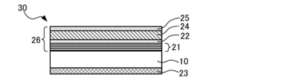
- FIG. 5 is a schematic diagram showing an example of the reflective mask blank 30 of the present invention.
- the reflective mask blank 30 of the present invention has a mask blank multilayer film 26 including a multilayer reflective film 21 and a phase shift film 24 on the main surface of the mask blank substrate 10.
- the mask blank multilayer film 26 includes the multilayer reflective film 21 and the phase shift film 24 formed on the main surface of the mask blank substrate 10 in the reflective mask blank 30. It is a plurality of films.
- the mask blank multilayer film 26 further includes a protective film 22 formed between the multilayer reflective film 21 and the phase shift film 24 and / or an etching mask film 25 formed on the surface of the phase shift film 24. it can.
- the mask blank multilayer film 26 on the main surface of the mask blank substrate 10 includes the multilayer reflective film 21, the protective film 22, the phase shift film 24, and the etching mask film. 25.
- “having the mask blank multilayer film 26 on the main surface of the mask blank substrate 10” means that the mask blank multilayer film 26 is disposed in contact with the surface of the mask blank substrate 10.
- “on (on the main surface)” includes both the meanings of “on” and “above” in English, and means “on / and / or above”.
- “the film A is disposed in contact with the surface of the film B” means that the film A and the film B are not interposed between the film A and the film B, It means that it is arranged so that it touches directly.
- FIG. 3 is a schematic diagram showing another example of the reflective mask blank 30 of the present invention.
- the mask blank multilayer film 26 includes the multilayer reflective film 21, the protective film 22, and the phase shift film 24, but does not include the etching mask film 25. .
- the reflective mask blank 30 of the present invention is a reflective mask blank in which a multilayer reflective film and a phase shift film for shifting the phase of EUV light are formed in this order on a substrate.
- the root mean square roughness (Rms) obtained by measuring with an atomic force microscope in a 1 ⁇ m ⁇ 1 ⁇ m region on the surface of the phase shift film 24 is 0.50 nm or less, and the space The power spectral density at a frequency of 10 to 100 ⁇ m ⁇ 1 is 17 nm 4 or less.
- the reflective mask blank 30 of the present invention When the reflective mask blank 30 of the present invention is used so that the absolute reflectance of the phase shift film 24 with respect to the UV light is designed to be in a predetermined range, the difference (deviation) from the design value is small and high. Since the phase shift film 24 having an absolute reflectance in the range can be obtained, the reflective mask 40 capable of obtaining high contrast at the edge portion of the phase shift film pattern 27 can be manufactured.
- Rms (Root means square), which is a representative surface roughness index, is a root mean square roughness, which is a square root of a value obtained by averaging the squares of deviations from the mean line to the measurement curve. Rms is expressed by the following formula (1).
- Equation (1) l is the reference length, and Z is the height from the average line to the measurement curve.
- Rmax which is a representative index of surface roughness, is the maximum height of the surface roughness, and the difference between the absolute value of the maximum value of the peak of the roughness curve and the maximum value of the depth of the valley. (The difference between the highest mountain and the deepest valley).
- Rms and Rmax are conventionally used for managing the surface roughness of the mask blank substrate 10 and are excellent in that the surface roughness can be grasped numerically.
- both Rms and Rmax are height information, and do not include information on a minute change in surface shape.
- the power spectrum analysis represented by the amplitude intensity at the spatial frequency can quantify the fine surface shape. If Z (x, y) is the height data in the x-coordinate and y-coordinate, the Fourier transform is given by the following equation (2).
- Nx and Ny are the numbers of data in the x and y directions.
- u 0, 1, 2,... Nx-1
- v 0, 1, 2,... Ny-1
- the spatial frequency f is given by the following equation (3).
- dx is the minimum resolution in the x direction
- dy is the minimum resolution in the y direction.
- the power spectral density PSD at this time is given by the following equation (4).
- Power spectrum analysis is excellent in that the change in the surface state of the phase shift film 24 of the reflective mask blank 30 can be grasped not only as a simple change in height but also as a change in the spatial frequency.
- Power spectrum analysis is a technique for analyzing the effects of microscopic reactions at the atomic level on the surface.
- the integral value I of power spectral density can be used.
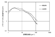
- the integral value I means an area in a range of a predetermined spatial frequency drawn by the value of the power spectral density (PSD) with respect to the spatial frequency as illustrated in FIG. 6, and is defined as Expression (5).
- the spatial frequency f is defined as shown in Equation (3), and the power spectral density is uniquely calculated as a function of the spatial frequency determined by the values of u and ⁇ .
- the spatial frequency f i is defined as in Equation (6).
- X ′ and N ′ are the measurement area and the number of data points.
- P (f i ) is the power spectral density at the spatial frequency f i .
- the surface of the phase shift film 24 is formed on the surface roughness (Rms) and the power spectral density, and an area of 1 ⁇ m ⁇ 1 ⁇ m is formed by atomic force.
- the root mean square roughness (Rms) obtained by measurement with a microscope is 0.50 nm or less, and the power spectral density at a spatial frequency of 10 to 100 ⁇ m ⁇ 1 is 17 nm 4 or less.
- the 1 ⁇ m ⁇ 1 ⁇ m region on the surface of the phase shift film 24 may be an arbitrary portion of the transfer pattern forming region.
- the transfer pattern forming region is, for example, a 142 mm ⁇ 142 mm region excluding the peripheral region on the surface of the reflective mask blank 30, 132 mm ⁇ 132 mm.
- an area of 132 mm ⁇ 104 mm, and the arbitrary portion can be, for example, a center area of the surface of the reflective mask blank 30.
- the 1 ⁇ m ⁇ 1 ⁇ m region can be a central region on the surface of the phase shift film 24.
- the center is an intersection of the rectangular diagonal lines. That is, the intersection and the center in the region (the center of the region is the same as the center of the film surface) coincide.
- the 1 ⁇ m ⁇ 1 ⁇ m region, the transfer pattern forming region, and an arbitrary portion described above can be applied to the mask blank substrate 10 and the multilayer reflective film-coated substrate 20 in some cases.
- the power spectral density at a spatial frequency of 10 to 100 ⁇ m ⁇ 1 obtained by measuring an area of 1 ⁇ m ⁇ 1 ⁇ m with an atomic force microscope on the surface of the phase shift film 24 of the reflective mask blank 30 should be 17 nm 4 or less. Can do.
- the power spectral density at a spatial frequency of 10 to 100 ⁇ m ⁇ 1 is 14 nm 4 or less, and more preferably the power spectral density at a spatial frequency of 10 to 100 ⁇ m ⁇ 1 is 10 nm 4 or less.
- the above-mentioned root mean square roughness (Rms) is 0.50 nm or less, preferably 0.45 nm or less, more preferably 0.40 nm or less, and further preferably 0.36 nm or less.
- the maximum height (Rmax) is preferably 5 nm or less, more preferably 4.5 nm or less, still more preferably 4 nm or less, and still more preferably 3.5 nm or less.
- the surface of the multilayer film 26 for mask blank 26 is obtained by measuring a 1 ⁇ m ⁇ 1 ⁇ m region with an atomic force microscope.
- the integral value I of the power spectral density of 100 ⁇ m ⁇ 1 is more preferably 360 nm 3 or less. More preferably, the integral value I is desirably 300 nm 3 or less. It is particularly preferable that the integral value I is 250 nm 3 or less.
- the reflective mask blank 30 of the present invention when the absolute phase reflectance of the phase phase shift film 24 is designed to be within a predetermined range, the difference (deviation) from the design value is reduced. A phase shift film 24 having a high absolute reflectance in a predetermined range can be obtained. Therefore, by using the reflective mask blank 30 of the present invention, it is possible to manufacture the reflective mask 40 that can obtain a high contrast at the edge portion of the phase shift film pattern 27.
- FIG. 1A is a perspective view showing an example of a mask blank substrate 10 that can be used for manufacturing the reflective mask blank 30 of the present invention.
- FIG. 1B is a schematic cross-sectional view of the mask blank substrate 10 shown in FIG.
- the mask blank substrate 10 (or simply referred to as “substrate 10” or “glass substrate 10”) is a rectangular plate-like body, and has two opposing main surfaces 2 and an end surface 1. .
- the two opposing main surfaces 2 are the upper surface and the lower surface of this plate-like body, and are formed so as to oppose each other. At least one of the two opposing main surfaces 2 is a main surface on which a transfer pattern is to be formed.
- the end face 1 is a side face of the plate-like body and is adjacent to the outer edge of the opposing main surface 2.
- the end surface 1 has a planar end surface portion 1d and a curved end surface portion 1f.
- the planar end surface portion 1d is a surface that connects the side of one opposing main surface 2 and the side of the other opposing main surface 2, and includes a side surface portion 1a and a chamfered slope portion 1b.
- the side surface portion 1a is a portion (T surface) substantially perpendicular to the opposing main surface 2 in the planar end surface portion 1d.
- the chamfered slope portion 1b is a chamfered portion (C surface) between the side surface portion 1a and the opposing main surface 2, and is formed between the side surface portion 1a and the opposing main surface 2.
- the curved end surface portion 1f is a portion (R portion) adjacent to the vicinity of the corner portion 10a of the substrate 10 when the substrate 10 is viewed in plan, and includes a side surface portion 1c and a chamfered slope portion 1e.
- the plan view of the substrate 10 refers to, for example, viewing the substrate 10 from a direction perpendicular to the opposing main surface 2.
- substrate 10 is the intersection vicinity of two sides in the outer edge of the opposing main surface 2, for example. The intersection of two sides may be the intersection of the extension lines of the two sides.
- the curved end surface portion 1 f is formed in a curved shape by rounding the corner 10 a of the substrate 10.
- the main surface of the mask blank substrate 10 used in the reflective mask blank 30 of the present invention and the surface of the multilayer reflective film 21 of the multilayer reflective film-coated substrate 20 are predetermined. It is preferable that the surface roughness is as follows.
- the main surface of the mask blank substrate 10 is preferably a surface processed by catalyst-based etching.
- Catalyst-based etching hereinafter referred to as “CARE” means that the workpiece (mask blank substrate) and the catalyst are placed in the processing solution, or the processing solution is supplied between the workpiece and the catalyst.
- CARE Catalyst-based etching
- the workpiece is brought into contact with the catalyst, and the workpiece is processed by active species generated from the molecules in the treatment liquid adsorbed on the catalyst at that time.
- the treatment liquid is water
- the workpiece and the catalyst are brought into contact with each other in the presence of water, and the catalyst and the workpiece surface are moved relative to each other. By doing so, the decomposition product by hydrolysis is removed from the surface of the workpiece and processed.
- the main surface of the mask blank substrate 10 is selectively surface-processed by the catalyst reference etching from the convex portions that are in contact with the catalyst surface as the reference surface. Therefore, the unevenness (surface roughness) constituting the main surface has a very uniform surface form while maintaining very high smoothness, and moreover, the ratio of forming the recesses rather than the protrusions with respect to the reference surface Many surface forms. Therefore, when a plurality of thin films are stacked on the main surface, the defect size of the main surface tends to be small, and therefore surface treatment by catalyst-based etching is preferable in terms of defect quality. In particular, the effect is particularly exerted when a multilayer reflective film 21 described later is formed on the main surface. Further, by subjecting the main surface to surface treatment by catalyst-based etching as described above, it is possible to relatively easily form a surface having the above-mentioned predetermined range of surface roughness and a predetermined power spectral density.
- the material of the substrate 10 is a glass material
- the catalyst at least one material selected from the group consisting of platinum, gold, transition metals, and alloys containing at least one of them can be used.
- the treatment liquid at least one kind of treatment liquid selected from the group consisting of functional water such as pure water, ozone water and hydrogen water, a low concentration alkaline aqueous solution, and a low concentration acidic aqueous solution can be used. .
- the mask blank substrate 10 used in the reflective mask blank 30 of the present invention is subjected to surface processing so that the main surface on which the transfer pattern is formed has high flatness from the viewpoint of obtaining at least pattern transfer accuracy and position accuracy. It is preferable.
- the flatness is 0.1 ⁇ m or less in the 132 mm ⁇ 132 mm region or 142 mm ⁇ 142 mm region of the main surface on the side where the transfer pattern of the substrate 10 is formed. Is particularly preferably 0.05 ⁇ m or less. More preferably, the flatness is 0.03 ⁇ m or less in the region of the main surface 132 mm ⁇ 132 mm on the side where the transfer pattern of the substrate 10 is formed.
- the main surface opposite to the side on which the transfer pattern is formed is a surface to be electrostatically chucked when being set in the exposure apparatus.
- the flatness of the main surface is preferably 1 ⁇ m or less, particularly preferably 0.5 ⁇ m or less, in a 142 mm ⁇ 142 mm region.
- any material may be used for the reflective mask blank substrate 10 for EUV exposure as long as it has low thermal expansion characteristics.
- SiO 2 —TiO 2 glass having characteristics of low thermal expansion binary system (SiO 2 —TiO 2 ) and ternary system (SiO 2 —TiO 2 —SnO 2 etc.)
- SiO 2 —Al 2 O A so-called multicomponent glass such as a 3- Li 2 O-based crystallized glass can be used.
- a substrate such as silicon or metal can also be used. Examples of the metal substrate include Invar alloy (Fe—Ni alloy).
- the substrate is required to have low thermal expansion characteristics.
- the multi-component glass material has a problem that it is difficult to obtain high smoothness as compared with synthetic quartz glass.
- a thin film made of a material made of a metal or an alloy, or a material containing at least one of oxygen, nitrogen, and carbon is formed on a substrate made of a multicomponent glass material. To do. And the surface of the surface roughness of the said range can be formed comparatively easily by carrying out mirror surface polishing and surface treatment of such a thin film surface.
- Ta tantalum
- an alloy containing Ta or a Ta compound containing at least one selected from oxygen, nitrogen, and carbon
- the Ta compound for example, TaB, TaN, TaO, TaON, TaCON, TaBN, TaBO, TaBON, TaBCON, TaHf, TaHfO, TaHfN, TaHfON, TaHfCON, TaSi, TaSiO, TaSiN, TaSiON, and TaSiCON are applied. Can do.
- the thin film preferably has an amorphous structure from the viewpoint of high smoothness on the surface of the thin film.
- the crystal structure of the thin film can be measured by an X-ray diffractometer (XRD).
- the processing method for obtaining the surface roughness specified above is not particularly limited.
- FIG. 2 is a schematic diagram showing an example of the multilayer reflective film-coated substrate 20 that can be used for the reflective mask blank 30.
- the substrate 20 with a multilayer reflective film of the present embodiment has a structure having the multilayer reflective film 21 on the main surface on the side where the transfer pattern of the mask blank substrate 10 described above is formed.
- the multilayer reflective film 21 provides a function of reflecting EUV light in the reflective mask 40 for EUV lithography, and has a configuration of the multilayer reflective film 21 in which elements having different refractive indexes are periodically stacked. .
- the material of the multilayer reflective film 21 is not particularly limited as long as it reflects EUV light.
- the single-layer reflectance of the multilayer reflective film 21 (absolute reflectance) is usually 65% or more, and the upper limit is usually 73%.
- the multilayer reflective film 21 includes 40 thin films (high refractive index layer) made of a high refractive index material and 40 thin films made of a low refractive index material (low refractive index layer) alternately.
- a multilayer reflective film 21 having about 60 cycles can be formed.
- the multilayer reflective film 21 for EUV light having a wavelength of 13 to 14 nm is preferably a Mo / Si periodic multilayer film in which Mo films and Si films are alternately stacked for about 40 periods.
- Ru / Si periodic multilayer film, Mo / Be periodic multilayer film, Mo compound / Si compound periodic multilayer film, Si / Nb periodic multilayer film, Si / Mo / Ru periodic multilayer films, Si / Mo / Ru / Mo periodic multilayer films, Si / Ru / Mo / Ru periodic multilayer films, Si / Ru / Mo / Ru periodic multilayer films, and the like can be used.
- the method for forming the multilayer reflective film 21 is known in the art, but can be formed by depositing each layer by, for example, a magnetron sputtering method or an ion beam sputtering method.
- a Si film having a thickness of about several nanometers is first formed on the substrate 10 using an Si target, for example, by ion beam sputtering. Thereafter, a Mo film having a thickness of several nanometers is formed using a Mo target.
- the Si reflection film and the Mo film are formed as one cycle, and the multilayer reflection film 21 is formed by laminating 40 to 60 cycles.
- the multilayer reflective film 21 is formed by ion beam sputtering by alternately irradiating a sputtering target of a high refractive index material and a sputtering target of a low refractive index material with an ion beam. It is preferred that By forming the multilayer reflective film 21 by a predetermined ion beam sputtering method, it is possible to obtain the multilayer reflective film 21 having good reflectance characteristics with respect to EUV light.
- the reflective mask blank 30 of the present invention further includes a protective film 22 in which the mask blank multilayer film 26 is disposed in contact with the surface of the multilayer reflective film 21 opposite to the mask blank substrate 10. It is preferable. That is, in the reflective mask blank 30 of the present invention, the protective film 22 is preferably formed on the multilayer reflective film 21.
- the protective film 22 (see FIG. 3) is used to protect the multilayer reflective film 21 from dry etching and wet cleaning in the manufacturing process of the reflective mask 40 for EUV lithography. ) Can also be formed.
- substrate 10 for mask blanks can also be set as the board
- the material of the protective film 22 examples include Ru, Ru— (Nb, Zr, Y, B, Ti, La, Mo), Si— (Ru, Rh, Cr, B), Si, Zr, Nb. Although materials such as La, B, and the like can be used, when a material containing ruthenium (Ru) is applied, the reflectance characteristics of the multilayer reflective film 21 become better.
- the material of the protective film 22 is preferably Ru or Ru— (Nb, Zr, Y, B, Ti, La, Mo).
- Such a protective film 22 is particularly effective when the phase shift film 24 is made of a Ta-based material and the phase shift film 24 is patterned by dry etching with a Cl-based gas.
- the power spectrum having a spatial frequency of 10 to 100 ⁇ m ⁇ 1 obtained by measuring an area of 1 ⁇ m ⁇ 1 ⁇ m with an atomic force microscope on the surface of the multilayer reflective film 21 or the protective film 22.
- density can be 7 nm 4 or less, preferably at most 6.5 nm 4 or less.
- the root mean square roughness (Rms) obtained by measuring with a force microscope is 0.15 nm or less, preferably 0.12 nm or less, and more preferably 0.10 nm or less.
- the substrate is formed during the formation of the multilayer reflective film 21 by sputtering.
- the high-refractive index layer and the low-refractive index layer can be deposited so that the sputtered particles are incident obliquely with respect to the normal line of the ten main surfaces. More specifically, the incident angle of the sputtered particles for forming the low refractive index layer such as Mo and the incident angle of the sputtered particles for forming the high refractive index layer such as Si are over 0 degree 45. It is preferable to form a film at a temperature below.
- the incident angle of the sputtered particles is more than 0 degree and 40 degrees or less, and more preferably more than 0 degree and 30 degrees or less.
- the protective film 22 formed on the multilayer reflective film 21 also has a protective film in which sputtered particles are incident obliquely with respect to the normal of the main surface of the substrate 10 after the multilayer reflective film 21 is formed. It is preferable to form by ion beam sputtering so that 22 is deposited.
- a back surface conductive film 23 (see FIG. 3) is formed on the surface of the substrate 10 opposite to the surface in contact with the multilayer reflective film 21 for the purpose of electrostatic chucking. Can do.
- the multilayer reflective film 21 and the protective film 22 are provided on the side on which the transfer pattern on the mask blank substrate 10 is formed, and the back surface conductive film 23 is provided on the surface opposite to the surface in contact with the multilayer reflective film 21.
- the form having the multilayer reflective film-coated substrate 20 in the present invention can also be used.
- the electrical characteristics (sheet resistance) required for the back conductive film 23 are usually 100 ⁇ / ⁇ or less.
- a method of forming the back conductive film 23 is known. For example, it can be formed using a target of a metal or alloy such as Cr or Ta by magnetron sputtering or ion beam sputtering.
- an underlayer may be formed between the substrate 10 and the multilayer reflective film 21.
- the underlayer can be formed for the purpose of improving the smoothness of the main surface of the substrate 10, for the purpose of reducing defects, for the purpose of enhancing the reflectivity of the multilayer reflective film 21, and for the purpose of correcting the stress of the multilayer reflective film 21.
- FIG. 3 is a schematic diagram showing an example of the reflective mask blank 30 of the present invention.
- the reflective mask blank 30 shown in FIG. 3 has a configuration in which a phase shift film 24 serving as a transfer pattern is formed on the protective film 22 of the substrate 20 with a multilayer reflective film described above.
- phase shift film 24 is formed on the multilayer reflective film 21 or on the protective film 22 formed on the multilayer reflective film 21.
- the phase shift film 24 absorbs EUV light and reflects a part thereof to shift the phase. That is, in the reflective mask 40 on which the phase shift film 24 is patterned, a portion where the phase shift film 24 remains is partially reflected so that the EUV light is absorbed and the pattern transfer is not affected.
- the EUV light reflected by the phase shift film 24 forms a phase difference with the reflected light from the multilayer reflective film 21.
- the phase shift film 24 is formed so that the absolute reflectance with respect to EUV light is 1 to 6%, and the phase difference between the reflected light from the phase shift film 24 and the reflected light from the multilayer reflective film 21 is 170 to 190 degrees.
- the film thickness of the phase shift film 24 is appropriately determined according to the material to be used and the design value of the absolute reflectance so that the phase difference is within the above range.
- the material of the phase shift film 24 is not particularly limited as long as it has a function of absorbing EUV light and can be removed by etching or the like.
- tantalum alone or a tantalum-based material containing tantalum is used as the phase shift film 24 from the viewpoint of etching selectivity and the like.
- tantalum-based materials include TaB alloys containing Ta and B, TaSi alloys containing Ta and Si, Ta alloys containing Ta and other transition metals (eg, Pt, Pd, Ag), and Ta It may be a tantalum compound obtained by adding N, O, H, and / or C to a metal or an alloy thereof.
- the phase shift film 24 composed of such tantalum or a tantalum compound can be formed by a known method such as a sputtering method such as a DC sputtering method or an RF sputtering method.
- the crystal state of the phase shift film 24 is preferably amorphous or microcrystalline from the viewpoint of smoothness. If the phase shift film 24 is not smooth, the edge roughness of the phase shift film pattern increases, and the dimensional accuracy of the pattern may deteriorate.
- a preferable surface roughness of the phase shift film 24 is a root mean square roughness (Rms) of 0.50 nm or less, more preferably Rms is 0.45 nm or less, further preferably Rms is 0.40 nm or less, and still more preferably. Rms is 0.36 nm.
- Ta has a large EUV light absorption coefficient, and can be easily dry-etched with a chlorine-based gas or a fluorine-based gas, so that it is a phase shift film material with excellent workability. Furthermore, by adding B and / or Si, Ge or the like to Ta, an amorphous material can be easily obtained, and the smoothness of the phase shift film 24 can be improved. Further, when N and / or O is added to Ta, the resistance of the phase shift film 24 to oxidation is improved, so that it is possible to improve the stability over time.
- the phase shift film 24 may be formed not only by a single tantalum material layer but also by laminating a plurality of tantalum material layers.
- the phase shift film 24 includes a film formed by stacking a tantalum-based material layer and another material layer.
- a chromium-based material layer and a ruthenium-based material layer can be used as the other material layers.
- a chromium-based material Cr alone, Cr alloy containing Cr and other transition metals (for example, Pt, Pd, and Ag), and Cr metal and / or Cr alloy include N, O, H, and C, etc.
- a chromium-based compound to which is added can be used as a chromium-based material.
- the ruthenium-based material may be a simple Ru metal or a Ru alloy containing a metal such as Nb, Zr, Y, B, Ti, La, Mo, Co and / or Re in Ru. Further, it may be a ruthenium compound obtained by adding N, O, H and / or C to a Ru metal or an alloy thereof.
- the phase shift film 24 is formed by a laminated structure of a tantalum material layer and another material layer (when another material layer is laminated on the tantalum material layer), the film formation starts and ends. It is preferable to form a film continuously without exposure to the atmosphere. By doing in this way, it can prevent that an oxide layer (tantalum oxide layer) is formed on the surface of a tantalum material layer. In that case, a step for removing the tantalum oxide layer is not required.
- the stacking order and the number of stacks of the tantalum material layer and the chromium material layer in the phase shift film 24 are not particularly limited.
- Ta / Cr two-layer structure, Cr / Ta two-layer structure, Ta / Cr / Ta three-layer structure, Cr / Ta / Cr three-layer structure, Ta / Cr / Ta / Cr It may be a four-layer structure, a four-layer structure of Cr / Ta / Cr / Ta, a four-layer structure of Ta / Ta / Cr / Cr, or a four-layer structure of Cr / Cr / Ta / Ta. It does not matter.
- the multilayer reflective film 21 or the material adjacent to the protective film 22 formed on the multilayer reflective film 21 is more preferably a tantalum material layer.
- the outermost surface layer of the phase shift film 24 can be a chromium-based material layer or a tantalum-based material layer (for example, a TaSi-based material layer).
- the outermost surface layer of the phase shift film 24 is more preferably a chromium-based material layer. This is because the chromium-based material layer can also function as an antioxidant film for the tantalum-based material layer. That is, when the chromium-based material layer is the uppermost layer, the tantalum-based material layer is prevented from being oxidized to lower the etching rate.
- the material of the outermost surface layer is a material containing nitrogen, specifically, from the viewpoint of controlling the power spectral density of the surface of the phase shift film. It is preferable to use CrN, CrON, CrCN, CrCON, CrHN, CrOHN, CrCHN, or CrCONH. Further, from the viewpoint of chemical resistance during mask cleaning, the material of the outermost layer is more preferably a material containing carbon, specifically, CrC, CrCO, CrCN, CrCON, CrCH, CrCOH, CrCHN, or CrCONH. .
- the chromium-based material and the tantalum-based material include nitrides, oxides, and alloys in addition to single metals, and may not necessarily have the same material and composition.
- the outermost surface layer of the phase shift film 24 can be a ruthenium-based material layer or a tantalum-based material layer (for example, a TaSi-based material layer).
- the material adjacent to the multilayer reflective film 21 or the protective film 22 formed on the multilayer reflective film 21 is more preferably a tantalum material layer, and the outermost surface layer of the phase shift film 24 is a ruthenium material. More preferably, it is a layer.
- the ruthenium-based material layer can also have a function as an antioxidant film for the tantalum-based material layer.
- the tantalum-based material and the ruthenium-based material include nitrides, oxides, and alloys in addition to single metals, and may not necessarily have the same material and composition.
- a tantalum-based material layer, a ruthenium-based material layer, and a chromium-based material layer may be stacked, and the stacking order and the number of stacked layers are not particularly limited.
- a three-layer structure of Ta / Ru / Cr or a three-layer structure of Ta / Cr / Ru may be used from the substrate 10 side, or other than these.
- the phase shift film 24 of the reflective mask blank 30 of the present invention preferably has a tantalum material layer containing tantalum and nitrogen, and a chromium material layer containing chromium and nitrogen on the tantalum material layer. Since the phase shift film 24 includes the tantalum material layer and the chromium material layer, it is possible to obtain a phase shift film having a predetermined phase shift effect and a high absolute reflectance with respect to EUV light.
- the film thickness of the chromium-based material layer is preferably 5 nm or more and 30 nm or less.
- the nitrogen content is preferably 5 atomic% or more and 50 atomic% or less, More preferably, it is 5 atomic% or more and 30 atomic% or less, and further preferably 5 atomic% or more and 20 atomic% or less.
- the phase shift film 24 includes a chromium-based material layer containing chromium and nitrogen
- the nitrogen content is preferably 5 atom% or more and 50 atom% or less, more preferably 5 atom% or more and 30 or less. Atomic% or less, More preferably, 5 atomic% or more and 20 atomic% or less are desirable.
- the phase shift film 24 includes a tantalum-based material layer containing tantalum and nitrogen
- the root mean square of the surface of the phase shift film 24 is obtained when the nitrogen content is 5 atomic% or more and 50 atomic% or less.
- the power spectrum density which is the roughness (Rms), and the amplitude intensity of all the roughness components having a spatial frequency of 10 to 100 ⁇ m ⁇ 1 that can be detected in the 1 ⁇ m ⁇ 1 ⁇ m region is within a predetermined value range.
- the phase shift film 24 includes a chromium-based material layer containing chromium and nitrogen
- the power spectral density is similarly determined when the nitrogen content is 5 atomic% or more and 50 atomic% or less. This is a range of values.
- the pattern edge roughness when the phase shift film 24 is patterned can be reduced.
- the root mean square roughness (Rms) obtained by measuring with an atomic force microscope in the 1 ⁇ m ⁇ 1 ⁇ m region on the surface of the phase shift film 24 and the spatial frequency of 10 to 100 ⁇ m.
- the power spectral density of ⁇ 1 is set to a value within a predetermined range.
- the reflective mask blank 30 of the present invention having such a structure is used and the phase shift film 24 is designed to have a high absolute reflectance with respect to EUV light, a difference (deviation) from the design value is obtained. ) Can be reduced to obtain a phase shift film 24 having a high absolute reflectance in a predetermined range. Therefore, by using the reflective mask blank 30 of the present invention, it is possible to manufacture the reflective mask 40 that can obtain a high contrast at the edge portion of the phase shift film pattern 27.
- the reflective mask blank 30 of the present invention is not limited to the configuration shown in FIG.
- a resist film serving as a mask for patterning the phase shift film 24 can be formed on the phase shift film 24.
- the reflective mask blank 30 with a resist film can also be used as the reflective mask blank 30 of the present invention.
- the resist film formed on the phase shift film 24 may be a positive type or a negative type. Further, it may be used for electron beam drawing or laser drawing.
- a so-called hard mask film (etching mask film 25) can be formed between the phase shift film 24 and the resist film.
- An embodiment including a hard mask film (etching mask film 25) can also be used as the reflective mask blank 30 in the present invention.
- the mask blank multilayer film 26 further includes an etching mask film 25 disposed in contact with the surface of the phase shift film 24 opposite to the mask blank substrate 10. It is preferable to include.
- the mask blank multilayer film 26 on the main surface of the mask blank substrate 10 is added to the multilayer reflective film 21, the protective film 22, and the phase shift film 24. Further, an etching mask film 25 is provided.
- the reflective mask blank 30 of the present invention can further have a resist film on the outermost surface of the mask blank multilayer film 26 of the reflective mask blank 30 shown in FIG.
- the reflective mask blank 30 of the present invention is formed with the etching mask film 25 made of a material containing tantalum.
- a structure is preferred.
- the reflective mask blank 30 of the present invention is made of a material containing chromium on the phase shift film 24. It is preferable that the etching mask film 25 to be formed has a structure.
- the etching mask film 25 is made of chlorine-based gas, fluorine-based gas, or Even if peeling is performed by dry etching using a mixed gas of chlorine-based gas and oxygen gas, good optical characteristics of the phase shift film pattern 27 can be obtained.
- Examples of the material containing tantalum for forming the etching mask film 25 include TaN, TaON, TaCON, TaBN, TaBON, TaBCON, TaHfN, TaHfON, TaHfCON, TaSiN, TaSiON, and TaSiCON.
- Examples of the material containing chromium that forms the etching mask film 25 include a material containing one or more elements selected from nitrogen, oxygen, carbon, and boron in chromium. Examples thereof include CrN, CrON, CrCN, CrCON, CrBN, CrBON, CrBCN, and CrBOCN. About the said material, you may contain metals other than chromium in the range with which the effect of this invention is acquired.
- the film thickness of the etching mask film 25 is desirably 3 nm or more from the viewpoint of obtaining a function as an etching mask for accurately forming the transfer pattern on the phase shift film 24.
- the thickness of the etching mask film 25 is desirably 15 nm or less from the viewpoint of reducing the thickness of the resist film.
- the surface of the etching mask film 25 is 1 ⁇ m ⁇ 1 ⁇ m in the same manner as when the outermost surface of the reflective mask blank 30 is the phase shift film 24.
- the root mean square roughness (Rms) obtained by measuring with an atomic force microscope and the power spectral density at a spatial frequency of 10 to 100 ⁇ m ⁇ 1 are set to a value within a predetermined range.
- the power spectral density of the film can also be managed.
- the reflective mask blank 30 of the present invention having such a structure is designed so that the absolute reflectance of the phase shift film 24 with respect to EUV light is in a predetermined range, the difference (deviation) from the design value is small.
- the phase shift film 24 having an absolute reflectance in a high predetermined range can be obtained. Therefore, by using the reflective mask blank 30 of the present invention having such a structure, a reflective mask 40 that can obtain high contrast at the edge portion of the phase shift film pattern 27 can be manufactured.
- the reflective mask blank 30 of the present invention includes a multilayer reflective film 21 and a phase shift film 24 in which high refractive index layers and low refractive index layers are alternately laminated on the main surface of the mask blank substrate 10.
- the step of forming the multilayer reflective film 21 on the main surface of the mask blank substrate 10 and the phase shift film 24 on the multilayer reflective film 21 are formed.
- the root mean square roughness (Rms) obtained by measuring with an atomic force microscope in the region of 1 ⁇ m ⁇ 1 ⁇ m of the surface of the reflective mask blank 30 is 0.
- the phase shift film 24 is formed so as to have a power spectral density of 50 nm or less and a spatial frequency of 10 to 100 ⁇ m ⁇ 1 of 17 nm 4 or less.
- Rms is 0.50 nm or less (preferably 0.45 nm or less, more preferably 0.40 nm or less, still more preferably 0.36 nm or less) on the surface of the phase shift film 24 of the reflective mask blank 30 of the present invention.
- the power spectral density which is the amplitude intensity of all roughness components having a spatial frequency of 10 to 100 ⁇ m ⁇ 1 that can be detected in a 1 ⁇ m ⁇ 1 ⁇ m region, is 17 nm 4 or less (preferably 14 nm 4 or less, more preferably 10 nm 4 or less).
- phase shift film 24 when the phase shift film 24 is designed so that the absolute reflectance with respect to the EUV light is in a predetermined range, the difference (deviation) from the design value is reduced, and the absolute reflectance in the high predetermined range is obtained.
- the phase shift film 24 can be obtained. Therefore, it is possible to manufacture the reflective mask 40 that can obtain high contrast at the edge portion of the phase shift film pattern 27.
- the phase shift film 24 is formed by a reactive sputtering method using a sputtering target made of a material included in the phase shift film 24.
- the phase shift film 24 is preferably formed so as to contain the components contained in the atmospheric gas during reactive sputtering.
- the reactive sputtering method by adjusting the flow rate of the atmospheric gas, the root mean square roughness (Rms) of the surface of the phase shift film 24 and the spatial frequency 10 that can be detected in the region of 1 ⁇ m ⁇ 1 ⁇ m.
- the power spectral density which is the amplitude intensity of all the roughness components of ⁇ 100 ⁇ m ⁇ 1 , can be adjusted to be within a predetermined value range.
- the atmospheric gas is preferably a mixed gas containing an inert gas and a nitrogen gas.
- the phase shift film 24 having an appropriate composition can be obtained.
- the phase shift film 24 having an appropriate root mean square roughness (Rms) and power spectral density can be reliably obtained on the surface of the phase shift film 24.
- the phase shift film 24 is composed of a TaN layer and a CrOCN layer
- an appropriate root mean square can be obtained by adjusting the flow rate of nitrogen during film formation in both the formation of the TaN layer and the formation of the CrOCN layer.
- the phase shift film 24 having the square root roughness (Rms) and the power spectral density can be reliably obtained.
- the phase shift film 24 is preferably formed using a sputtering target made of a material containing tantalum. As a result, it is possible to form the phase shift film 24 having an absorptance for appropriate EUV light containing tantalum.
- the manufacturing method of the reflective mask blank 30 of the present invention preferably further includes a step of forming a protective film 22 disposed in contact with the surface of the multilayer reflective film 21.
- a protective film 22 disposed in contact with the surface of the multilayer reflective film 21.
- the protective film 22 is preferably formed by an ion beam sputtering method in which a sputtering target made of the protective film 22 is irradiated with an ion beam. Since the surface of the protective film can be smoothed by the ion beam sputtering method, the surface of the phase shift film formed on the protective film or the etching mask film formed on the phase shift film can be smoothed. .
- the manufacturing method of the reflective mask blank 30 of the present invention preferably further includes a step of forming an etching mask film 25 disposed in contact with the surface of the phase shift film 24.
- a highly accurate transfer pattern can be formed when the transfer pattern is formed on the phase shift film 24.
- FIG. 4 is a schematic diagram showing the reflective mask 40 of the present embodiment.
- the reflective mask 40 of the present invention has a configuration in which the phase shift film 24 in the reflective mask blank 30 is patterned to form a phase shift film pattern 27 on the multilayer reflective film 21 or the protective film 22. .
- exposure light such as EUV light
- the reflective mask 40 of this embodiment is exposed to exposure light such as EUV light
- the exposure light is absorbed in a portion of the mask surface where the phase shift film 24 is present, and the other portions where the phase shift film 24 is removed are exposed. Since the exposure light is reflected by the protective film 22 and the multilayer reflective film 21, the reflective mask 40 for lithography can be used.
- the reflective mask 40 of the present invention When the reflective mask 40 of the present invention is designed so that the absolute reflectance of the phase shift film 24 with respect to EUV light is in a predetermined range, the difference (deviation) from the design value is reduced, and the high predetermined range. A phase shift film 24 having an absolute reflectance can be obtained. Therefore, in the reflective mask 40 of the present invention, high contrast can be obtained at the edge portion of the phase shift film pattern 27.
- the patterning of the phase shift film 24 can be performed as follows. That is, first, a resist film pattern is formed on the surface of the phase shift film 24. By using the resist film pattern as a mask and performing dry etching with an etching gas, the phase shift film 24 is etched and a phase shift film pattern is formed. As the etching gas at this time, chlorine gas such as Cl 2 , SiCl 4 , CHCl 3 and CCl 4 , a mixed gas containing these chlorine gas and O 2 at a predetermined ratio, chlorine gas and He are predetermined.
- chlorine gas such as Cl 2 , SiCl 4 , CHCl 3 and CCl 4
- a mixed gas containing these chlorine gas and O 2 at a predetermined ratio chlorine gas and He are predetermined.
- etching with an etching gas suitable for each material can be performed a plurality of times.
- a reflective mask 40 for EUV lithography that achieves high reflectivity.
- the resist film can be removed at the same time as etching one layer of the laminated structure of the phase shift film 24. In this case, a process only for removing the resist film pattern is not necessary. Further, when the etching mask film 25 is provided, a process for removing the etching mask film 25 may be separately required.
- the reflective mask blank 30 has the protective film 22 on the multilayer reflective film 21
- damage to the surface of the multilayer reflective film 21 when the reflective mask 40 (EUV mask) is manufactured can be suppressed. Therefore, it is preferable that the reflective mask 40 also has the protective film 22 on the multilayer reflective film 21. As a result, the reflectance characteristics of the reflective mask 40 with respect to EUV light are improved.
- the reflective mask 40 of the present invention has a root mean square roughness (Rms) of 0.15 nm or less obtained by measuring with an atomic force microscope in a 1 ⁇ m ⁇ 1 ⁇ m region on the surface of the multilayer reflective film 21 or the protective film 22.
- the power spectral density at a spatial frequency of 10 to 100 ⁇ m ⁇ 1 is preferably 7 nm 4 or less.
- the difference between the power spectral density on the surface of the phase shift film pattern 27 and the power spectral density on the surface of the multilayer reflective film 21 or the protective film 22 is preferably 10 nm 4 or less.
- the difference in the predetermined power spectral density is in the predetermined range, the reflective mask 40 that can obtain a high contrast at the edge portion of the phase shift film pattern 27 can be obtained more reliably.
- a circuit pattern or the like based on the phase shift film pattern 27 of the reflective mask 40 is formed on a resist film formed on a transfer target such as a semiconductor substrate by a lithography process using the reflective mask 40 described above and an exposure apparatus.
- a semiconductor device in which various transfer patterns and the like are formed on a transfer target such as a semiconductor substrate can be manufactured.
- the reflective mask 40 capable of obtaining a high contrast at the edge portion of the phase shift film pattern can be used, a resist film formed on a transfer target such as a semiconductor substrate.
- a semiconductor device having a transfer pattern with a precise and fine transfer pattern such as a circuit pattern to be transferred can be manufactured.
- the multilayer reflective film 21 and the phase shift film 24 were formed on the surface of the mask blank substrate 10 for EUV exposure as described below. Further, the back surface conductive film 23 was formed on the back surface of the mask blank substrate 10 to manufacture the reflective mask blanks 30 of Examples 1 to 3 and Comparative Example 1. Therefore, the reflective mask blanks 30 of Examples 1 to 3 and Comparative Example 1 have the structure of the back conductive film 23 / the mask blank substrate 10 / the multilayer reflective film 21 / the protective film 22 / the phase shift film 24.
- a SiO 2 —TiO 2 glass substrate 10 having a size of 152 mm ⁇ 152 mm and a thickness of 6.35 mm is prepared as a mask blank substrate 10, and the front and back surfaces of the glass substrate 10 are attached using a double-side polishing apparatus. After polishing stepwise with cerium oxide abrasive grains or colloidal silica abrasive grains, surface treatment was performed with low-concentration silicic acid. When the surface roughness of the surface of the glass substrate 10 thus obtained was measured with an atomic force microscope, the root mean square roughness (Rms) was 0.5 nm.
- the surface shape (surface form, flatness) and TTV (plate thickness variation) of a region of 148 mm ⁇ 148 mm on the front and back surfaces of the glass substrate 10 were measured with a wavelength shift interferometer using a wavelength modulation laser.
- the flatness of the front and back surfaces of the glass substrate 10 was 290 nm (convex shape).
- the measurement result of the surface shape (flatness) of the surface of the glass substrate 10 is stored in a computer as height information with respect to a reference plane at each measurement point, and the reference value 50 nm (convexity) of the surface flatness necessary for the glass substrate 10 is used.
- Shape) and the back flatness standard value of 50 nm, and the difference (necessary removal amount) was calculated by a computer.
- the processing conditions for local surface processing according to the required removal amount were set for each processing spot shape region in the surface of the glass substrate 10.
- the dummy substrate was processed with spots without moving the substrate for a certain period of time as in the actual processing.
- the shape was measured with the same measuring device as the apparatus for measuring the surface shape of the front and back surfaces, and the processing volume of the spot per unit time was calculated.
- the scanning speed for raster scanning the glass substrate 10 was determined.
- the flatness of the front and back surfaces of the glass substrate 10 is less than the above-mentioned reference value by a magnetic viscoelastic fluid polishing (Magneto Rheological Finishing: MRF) processing method using a substrate finishing apparatus using magnetic fluid.
- MRF Magnetic Rheological Finishing
- the surface shape was adjusted by local surface processing.
- the magnetic viscoelastic fluid used at this time contained an iron component, and the polishing slurry was an alkaline aqueous solution containing about 2 wt% of cerium oxide as an abrasive.
- the local processing method of the mask blank substrate 10 in the present invention is not limited to the above-described magnetic viscoelastic fluid polishing processing method.
- a processing method using a gas cluster ion beam (Gas Cluster Ion Beams: GCIB) and a local plasma may be used.
- the spectral density was a maximum value of 5.29 nm 4 and a minimum value of 1.15 nm.
- the power spectral density at a spatial frequency of 10 ⁇ m ⁇ 1 to 100 ⁇ m ⁇ 1 was a maximum value of 1.18 nm 4 and a minimum value of 0.20 nm 4 .
- the incident angles of Mo and Si sputtered particles with respect to the normal of the main surface of the glass substrate 10 in ion beam sputtering were 30 degrees, and the gas flow rate of the ion source was 8 sccm. .
- a Ru protective film 22 (film thickness 2.5 nm) was continuously formed on the multilayer reflective film 21 by ion beam sputtering to obtain a substrate 20 with a multilayer reflective film.
- the incident angle of Ru sputtered particles with respect to the normal of the main surface of the substrate was 40 degrees, and the gas flow rate of the ion source was 8 sccm.
- a phase shift film 24 was formed on the main surface of the mask blank substrate 10 by the DC magnetron sputtering method.
- a laminated film composed of two layers of a TaN layer and a CrOCN layer was used as the phase shift film 24.
- phase shift film 24 of Examples 1 to 3 and Comparative Example 1 a TaN layer (tantalum-based material layer) and a CrCON layer (chromium-based material layer) were laminated by DC sputtering to form the phase shift film 24.
- the elemental composition of the TaN layer and CrCON layer was measured by X-ray photoelectron spectroscopy (XPS method).
- the TaN layer is a TaN layer having a predetermined thickness shown in Table 1 (Ta: 92.5 at%, N: 7) by a reactive sputtering method in a mixed gas atmosphere of Ar gas and N 2 gas using a tantalum target. .5 at%) was formed.
- the CrCON layer uses a chromium target and is reactive sputtering in a mixed gas atmosphere of Ar gas, CO 2 gas, and N 2 gas, and has a predetermined thickness shown in Table 1 (Cr: 45 at%, C: 10 at%, O: 35 at%, N: 10 at%) were formed (continuous film formation from the TaN film to the formation of the CrCON film without exposure to the atmosphere).
- the deposition pressure at the time of forming the TaN films of Examples 1 to 3 was 0.08 Pa. Further, the deposition pressure at the time of forming the TaN film of Comparative Example 1 was set to 0.12 Pa, which was higher than those in Examples 1 to 3.
- the deposition pressure of the CrOCN films of Examples 1 to 3 and Comparative Example 1 was 0.12 Pa.
- the refractive index n and extinction coefficient k at a wavelength of 13.5 nm of the TaN layer and the CrCON layer constituting the phase shift film 24 formed as described above were as follows.
- the film thicknesses of the TaN layer and the CrCON layer are set so that the absolute reflectance of the phase shift film 24 is 2.4 to 2.8% and the phase difference is 180 degrees at a wavelength of 13.5 nm. .
- a reflective mask blank 30 of Examples 1 to 3 and Comparative Example 1 was manufactured by forming a back conductive film 23 on the back surface of the mask blank substrate 10.
- FIG. 6 shows the results of power spectrum analysis of Example 3 and Comparative Example 1.
- the power spectral density at a spatial frequency of 10 to 100 ⁇ m ⁇ 1 obtained by measuring an area of 1 ⁇ m ⁇ 1 ⁇ m on the surface of the phase shift film 24 of Example 3 with an atomic force microscope has a maximum value of 15 It was .56 nm 4 and the minimum value was 0.69 nm 4 .
- the power spectral density at a spatial frequency of 10 to 100 ⁇ m ⁇ 1 obtained by measuring an area of 1 ⁇ m ⁇ 1 ⁇ m on the surface of the phase shift film 24 of Comparative Example 1 with an atomic force microscope is maximum. The value was 21.63 nm 4 , and the minimum value was 1.52 nm 4 .
- the root mean square roughness (Rms) obtained by measuring with an atomic force microscope in the 1 ⁇ m ⁇ 1 ⁇ m region of the surface of the phase shift film 24 of Examples 1 to 3 is 0.50 nm or less. Met.
- the root mean square roughness (Rms) obtained by measuring with an atomic force microscope in the 1 ⁇ m ⁇ 1 ⁇ m region of the surface of the phase shift film 24 of Comparative Example 1 was 0.447 nm.
- the maximum value of the power spectral density at a spatial frequency of 10 to 100 ⁇ m ⁇ 1 on the surface of the phase shift film 24 of Examples 1 to 3 was 17 nm 4 or less.
- the maximum value of the power spectral density in the spatial frequency 10 ⁇ 100 [mu] m -1 of the surface of the phase shift film 24 of Comparative Example 1 is greater than 17 nm 4, it was 21.63nm 4.
- Table 1 shows (A) the power spectral density (PSD) of the surface of the phase shift film and (B) the power of the surface of the multilayer reflective film (with a protective film) after the production of the reflective masks of Examples 1 to 3 and Comparative Example 1.
- PSD power spectral density
- the difference (A ⁇ B) between (A) and (B) in Examples 1 to 3 was 10 nm 4 or less.
- Difference in Comparative Example 1 (A) and (B) contrast (A-B) is 15.17Nm 4, was greater than 10 nm 4.
- the root mean square roughness Rms of the surfaces of the multilayer reflective films (with a protective film) of Examples 1 to 3 and Comparative Example 1 was 0.138 nm, which was 0.15 nm or less.
- PSD maximum spatial frequency 10 ⁇ 100 ⁇ m -1 of Examples 1 to 3 and the multilayer reflective film (with protective film) of Comparative Example 1 surface is 6.46nm 4, it was 7 nm 4 or less.
- Table 1 shows a design value, a measured value, and a difference (deviation) between the measured value and the absolute reflectance RPSM of the phase shift film 24 of Examples 1 to 3 and Comparative Example 1.
- the absolute reflectance RPSM of the phase shift film 24 was measured using an EUV reflectance measurement (LPR-1016) apparatus. At this time, EUV light having a wavelength of 13.5 nm was used as measurement light for measuring absolute reflectance.
- the absolute reflectance R ML of the multilayer reflective film surface was 65%.
- the absolute reflectance RPSM of the phase shift films 24 of Examples 1 to 3 is as high as 2.0% or more, and the difference (deviation) between the design value and the measured value of the absolute reflectance RPSM.
- a resist was applied by spin coating on the surface of the phase shift film 24 of the reflective mask blank 30 of Examples 1 to 3 and Comparative Example 1, and a resist film having a thickness of 150 nm was formed through heating and cooling processes. .
- a resist pattern was formed through a drawing and developing process of a desired pattern.
- the phase shift film 24 was patterned by predetermined dry etching to form a phase shift film pattern 27 on the protective film 22.
- the phase shift film 24 is a laminated film composed of two layers of TaN layer and CrOCN layer, mixing of chlorine (Cl 2), and mixed gas of oxygen (O 2) (chlorine (Cl 2) and oxygen (O 2)
- the ratio can be dry etched by 4: 1).
- the multilayer reflective film 21 and the protective film 22 were formed on the main surface of the mask blank substrate 10 on the side where the transfer pattern is formed. Then, although the back surface conductive film 23 was formed in the back surface on the opposite side to the said main surface, it is not restricted to this. After the back surface conductive film 23 is formed on the main surface opposite to the main surface on which the transfer pattern of the mask blank substrate 10 is formed, the multilayer reflective film 21 is formed on the main surface on which the transfer pattern is formed. Further, the reflective mask blank 30 may be manufactured by forming the protective film 22 to form the multilayer reflective film-coated substrate 20 and further forming the phase shift film 24 on the protective film 22.
Landscapes
- Chemical & Material Sciences (AREA)
- General Chemical & Material Sciences (AREA)
- Life Sciences & Earth Sciences (AREA)
- Engineering & Computer Science (AREA)
- Chemical Kinetics & Catalysis (AREA)
- Geochemistry & Mineralogy (AREA)
- Materials Engineering (AREA)
- Organic Chemistry (AREA)
- General Physics & Mathematics (AREA)
- Physics & Mathematics (AREA)
- Preparing Plates And Mask In Photomechanical Process (AREA)
- Exposure And Positioning Against Photoresist Photosensitive Materials (AREA)
- Exposure Of Semiconductors, Excluding Electron Or Ion Beam Exposure (AREA)
Abstract
Description
本発明の構成1は、基板上に多層反射膜と、EUV光の位相をシフトさせる位相シフト膜とがこの順に形成された反射型マスクブランクであって、前記位相シフト膜表面における1μm×1μm領域において、原子間力顕微鏡で測定して得られる二乗平均平方根粗さ(Rms)が0.50nm以下であり、かつ空間周波数10~100μm-1のパワースペクトル密度が17nm4以下であることを特徴とする反射型マスクブランクである。
本発明の構成2は、前記多層反射膜上に保護膜が形成されていることを特徴とする構成1に記載の反射型マスクブランクである。
本発明の構成3は、前記位相シフト膜は、タンタルと窒素を含むタンタル系材料層と、前記タンタル系材料層上にクロム及び窒素を含むクロム系材料層とを有することを特徴とする構成1又は2に記載の反射型マスクブランクである。
本発明の構成4は、前記クロム系材料層の膜厚は、5nm以上30nm以下であることを有することを特徴とする構成3に記載の反射型マスクブランクである。
本発明の構成5は、基板上に多層反射膜と、EUV光の位相をシフトさせる位相シフト膜パターンとがこの順に形成された反射型マスクであって、前記位相シフト膜パターン表面における1μm×1μm領域において、原子間力顕微鏡で測定して得られる二乗平均平方根粗さ(Rms)が0.50nm以下であり、かつ空間周波数10~100μm-1のパワースペクトル密度が17nm4以下であることを特徴とする反射型マスクである。
本発明の構成6は、前記多層反射膜上に保護膜が形成されていることを特徴とする構成5に記載の反射型マスクである。
本発明の構成7は、前記多層反射膜又は前記保護膜表面における1μm×1μm領域において、原子間力顕微鏡で測定して得られる二乗平均平方根粗さ(Rms)が0.15nm以下であり、かつ空間周波数10~100μm-1のパワースペクトル密度が7nm4以下であることを特徴とする構成5又は6に記載の反射型マスクである。
本発明の構成8は、前記位相シフト膜パターン表面のパワースペクトル密度と、前記多層反射膜又は前記保護膜表面におけるパワースペクトル密度との差が10nm4以下であることを特徴とする構成5~7に記載の反射型マスクである。

式(1)において、lは基準長さであり、Zは平均線から測定曲線までの高さである。


ここで、式(3)において、dxはx方向の最小分解能であり、dyはy方向の最小分解能である。



まず、本発明の反射型マスクブランク30の製造に用いることのできるマスクブランク用基板10について以下に説明する。
次に、本発明の反射型マスクブランク30に用いることのできる多層反射膜付き基板20について以下に説明する。
次に、本発明の反射型マスクブランク30について説明する。
多層反射膜21の上、又は多層反射膜21の上に形成された保護膜22の上に、位相シフト膜24が形成される。位相シフト膜24は、EUV光を吸収するとともに一部を反射させて位相をシフトさせるものである。即ち、位相シフト膜24がパターンニングされた反射型マスク40において、位相シフト膜24が残っている部分では、EUV光を吸収しつつパターン転写に影響がないように一部を反射させる。位相シフト膜24で反射したEUV光は、多層反射膜21からの反射光との位相差を形成する。位相シフト膜24は、EUV光に対する絶対反射率が1~6%、位相シフト膜24からの反射光と多層反射膜21からの反射光との位相差が170~190度となるように形成される。位相シフト膜24の膜厚は、用いる材料及び絶対反射率の設計値に応じて、且つ、位相差が上記範囲内に入る条件となるように適宜定められる。
本発明の反射型マスクブランク30では、マスクブランク用多層膜26が、位相シフト膜24の表面のうち、マスクブランク用基板10とは反対側の表面に接して配置されるエッチングマスク膜25を更に含むことが好ましい。図5に示す反射型マスクブランク30の場合には、マスクブランク用基板10の主表面の上のマスクブランク用多層膜26が、多層反射膜21、保護膜22及び位相シフト膜24に加えて、更にエッチングマスク膜25を有している。本発明の反射型マスクブランク30は、図5に示す反射型マスクブランク30のマスクブランク用多層膜26の最表面に、更にレジスト膜を有することができる。
次に、本発明の反射型マスクブランク30の製造方法について説明する。
次に、本発明の一実施形態に係る反射型マスク40について以下に説明する。
以上説明した反射型マスク40と、露光装置を使用したリソグラフィープロセスにより、半導体基板等の被転写体上に形成されたレジスト膜に、反射型マスク40の位相シフト膜パターン27に基づく回路パターン等の転写パターンを転写し、その他種々の工程を経ることで、半導体基板等の被転写体上に種々の転写パターン等が形成された半導体装置を製造することができる。
マスクブランク用基板10として、大きさが152mm×152mm、厚さが6.35mmのSiO2-TiO2系のガラス基板10を準備し、両面研磨装置を用いて、当該ガラス基板10の表裏面を、酸化セリウム砥粒やコロイダルシリカ砥粒により段階的に研磨した後、低濃度のケイフッ酸で表面処理した。これにより得られたガラス基板10表面の表面粗さを原子間力顕微鏡で測定したところ、二乗平均平方根粗さ(Rms)は0.5nmであった。
加工液:純水
触媒:白金
基板回転数:10.3回転/分
触媒定盤回転数:10回転/分
加工時間:50分
加工圧:250hPa
Moターゲット及びSiターゲットを使用して、イオンビームスパッタリングによりMo層(低屈折率層、厚み2.8nm)及びSi層(高屈折率層、厚み4.2nm)を交互積層し(積層数40ペア)、最後にSi層を4.0nmの厚みで成膜し、多層反射膜21を上述のガラス基板10上に形成した。イオンビームスパッタリング法による多層反射膜21の成膜の際、イオンビームスパッタリングにおけるガラス基板10の主表面の法線に対するMo及びSiスパッタ粒子の入射角度は30度、イオンソースのガス流量は8sccmとした。
TaN層:n=0.94、k=0.034
CrCON層:n=0.93、k=0.037
なお、上記、TaN層及びCrCON層の膜厚は、波長13.5nmにおいて位相シフト膜24の絶対反射率が2.4~2.8%、位相差が180度となるように設定してある。

実施例1~3及び比較例1の反射型マスクブランク30の位相シフト膜24の表面に、スピンコート法によりレジストを塗布し、加熱及び冷却工程を経て、膜厚150nmのレジスト膜を成膜した。次いで、所望のパターンの描画及び現像工程を経て、レジストパターン形成した。当該レジストパターンをマスクにして、所定のドライエッチングにより、位相シフト膜24のパターニングを行い、保護膜22上に位相シフト膜パターン27を形成した。なお、TaN層及びCrOCN層の二層からなる積層膜である位相シフト膜24は、塩素(Cl2)及び酸素(O2)の混合ガス(塩素(Cl2)及び酸素(O2)の混合比(流量比)は4:1)によりドライエッチングすることができる。
上述の実施例1~3及び比較例1の反射型マスク40を使用し、露光装置を使用して、半導体基板である被転写体上のレジスト膜にパターン転写を行い、その後、配線層をパターニングして、半導体装置を作製すると、反射型マスクの位相シフト膜パターンのエッジ部で高いコントラストを得るため、転写パターンの寸法が正確な半導体装置を作製することができる。
20 多層反射膜付き基板
21 多層反射膜
22 保護膜
23 裏面導電膜
24 位相シフト膜
25 エッチングマスク膜
26 マスクブランク用多層膜
27 位相シフト膜パターン
30 反射型マスクブランク
40 反射型マスク
Claims (9)
- 基板上に多層反射膜と、EUV光の位相をシフトさせる位相シフト膜とがこの順に形成された反射型マスクブランクであって、
前記位相シフト膜表面における1μm×1μm領域において、原子間力顕微鏡で測定して得られる二乗平均平方根粗さ(Rms)が0.50nm以下であり、かつ空間周波数10~100μm-1のパワースペクトル密度が17nm4以下であることを特徴とする反射型マスクブランク。 - 前記多層反射膜上に保護膜が形成されていることを特徴とする請求項1に記載の反射型マスクブランク。
- 前記位相シフト膜は、タンタルと窒素を含むタンタル系材料層と、前記タンタル系材料層上にクロム及び窒素を含むクロム系材料層とを有することを特徴とする請求項1又は2に記載の反射型マスクブランク。
- 前記クロム系材料層の膜厚は、5nm以上30nm以下であることを有することを特徴とする請求項3に記載の反射型マスクブランク。
- 基板上に多層反射膜と、EUV光の位相をシフトさせる位相シフト膜パターンとがこの順に形成された反射型マスクであって、
前記位相シフト膜パターン表面における1μm×1μm領域において、原子間力顕微鏡で測定して得られる二乗平均平方根粗さ(Rms)が0.50nm以下であり、かつ空間周波数10~100μm-1のパワースペクトル密度が17nm4以下であることを特徴とする反射型マスク。 - 前記多層反射膜上に保護膜が形成されていることを特徴とする請求項5に記載の反射型マスク。
- 前記多層反射膜又は前記保護膜表面における1μm×1μm領域において、原子間力顕微鏡で測定して得られる二乗平均平方根粗さ(Rms)が0.15nm以下であり、かつ空間周波数10~100μm-1のパワースペクトル密度が7nm4以下であることを特徴とする請求項5又は6に記載の反射型マスク。
- 前記位相シフト膜パターン表面のパワースペクトル密度と、前記多層反射膜又は前記保護膜表面におけるパワースペクトル密度との差が10nm4以下であることを特徴とする請求項5~7に記載の反射型マスク。
- 請求項5~8のいずれか1項に記載の反射型マスクを用いて、露光装置を使用したリソグラフィープロセスを行い、被転写体上に転写パターンを形成する工程を有する半導体装置の製造方法。
Priority Applications (4)
| Application Number | Priority Date | Filing Date | Title |
|---|---|---|---|
| KR1020177020000A KR102545187B1 (ko) | 2014-12-24 | 2015-12-15 | 반사형 마스크 블랭크, 반사형 마스크 및 반도체 장치의 제조방법 |
| US15/539,263 US10394113B2 (en) | 2014-12-24 | 2015-12-15 | Reflective mask blank, reflective mask and method of manufacturing semiconductor device |
| KR1020237020102A KR102561655B1 (ko) | 2014-12-24 | 2015-12-15 | 반사형 마스크 블랑크, 반사형 마스크, 및 반도체 장치의 제조 방법 |
| US16/504,151 US10642149B2 (en) | 2014-12-24 | 2019-07-05 | Reflective mask blank, reflective mask and method of manufacturing semiconductor device |
Applications Claiming Priority (2)
| Application Number | Priority Date | Filing Date | Title |
|---|---|---|---|
| JP2014-260280 | 2014-12-24 | ||
| JP2014260280A JP6499440B2 (ja) | 2014-12-24 | 2014-12-24 | 反射型マスクブランク及び反射型マスク |
Related Child Applications (2)
| Application Number | Title | Priority Date | Filing Date |
|---|---|---|---|
| US15/539,263 A-371-Of-International US10394113B2 (en) | 2014-12-24 | 2015-12-15 | Reflective mask blank, reflective mask and method of manufacturing semiconductor device |
| US16/504,151 Continuation US10642149B2 (en) | 2014-12-24 | 2019-07-05 | Reflective mask blank, reflective mask and method of manufacturing semiconductor device |
Publications (1)
| Publication Number | Publication Date |
|---|---|
| WO2016104239A1 true WO2016104239A1 (ja) | 2016-06-30 |
Family
ID=56150264
Family Applications (1)
| Application Number | Title | Priority Date | Filing Date |
|---|---|---|---|
| PCT/JP2015/085020 Ceased WO2016104239A1 (ja) | 2014-12-24 | 2015-12-15 | 反射型マスクブランク、反射型マスク及び半導体装置の製造方法 |
Country Status (5)
| Country | Link |
|---|---|
| US (2) | US10394113B2 (ja) |
| JP (1) | JP6499440B2 (ja) |
| KR (2) | KR102545187B1 (ja) |
| TW (2) | TWI682232B (ja) |
| WO (1) | WO2016104239A1 (ja) |
Cited By (3)
| Publication number | Priority date | Publication date | Assignee | Title |
|---|---|---|---|---|
| WO2019225737A1 (ja) * | 2018-05-25 | 2019-11-28 | Hoya株式会社 | 反射型マスクブランク、反射型マスク、並びに反射型マスク及び半導体装置の製造方法 |
| US10915015B2 (en) | 2017-12-21 | 2021-02-09 | Samsung Electronics Co., Ltd. | EUV mask blank, photomask manufactured by using the EUV mask blank, lithography apparatus using the photomask and method of fabricating semiconductor device using the photomask |
| TWI925363B (zh) | 2018-05-25 | 2026-05-11 | 日商Hoya股份有限公司 | 反射型光罩基底及反射型光罩 |
Families Citing this family (15)
| Publication number | Priority date | Publication date | Assignee | Title |
|---|---|---|---|---|
| JP6740107B2 (ja) * | 2016-11-30 | 2020-08-12 | Hoya株式会社 | マスクブランク、転写用マスク及び半導体デバイスの製造方法 |
| JP6861095B2 (ja) * | 2017-03-03 | 2021-04-21 | Hoya株式会社 | 反射型マスクブランク、反射型マスク及び半導体装置の製造方法 |
| KR20240025717A (ko) | 2017-03-03 | 2024-02-27 | 호야 가부시키가이샤 | 반사형 마스크 블랭크, 반사형 마스크 및 반도체 장치의 제조 방법 |
| TWI835798B (zh) * | 2018-05-25 | 2024-03-21 | 日商Hoya股份有限公司 | 反射型光罩基底、反射型光罩及其製造方法、以及半導體裝置之製造方法 |
| TWI847949B (zh) * | 2018-11-30 | 2024-07-01 | 日商Hoya股份有限公司 | 光罩基底、光罩之製造方法及顯示裝置之製造方法 |
| JP6929340B2 (ja) | 2019-11-21 | 2021-09-01 | Hoya株式会社 | 反射型マスクブランクおよび反射型マスク、並びに半導体装置の製造方法 |
| JP7280171B2 (ja) * | 2019-12-05 | 2023-05-23 | 信越化学工業株式会社 | フォトマスクブランク、フォトマスクの製造方法及びフォトマスク |
| US11111176B1 (en) * | 2020-02-27 | 2021-09-07 | Applied Materials, Inc. | Methods and apparatus of processing transparent substrates |
| JP7318565B2 (ja) * | 2020-03-03 | 2023-08-01 | 信越化学工業株式会社 | 反射型マスクブランクの製造方法 |
| JP6929983B1 (ja) * | 2020-03-10 | 2021-09-01 | Hoya株式会社 | 反射型マスクブランクおよび反射型マスク、並びに半導体デバイスの製造方法 |
| KR20210155863A (ko) * | 2020-06-16 | 2021-12-24 | 삼성전자주식회사 | 극자외선 리소그래피용 위상 반전 마스크 및 이를 이용한 반도체 소자의 제조 방법 |
| US11940725B2 (en) | 2021-01-27 | 2024-03-26 | S&S Tech Co., Ltd. | Phase shift blankmask and photomask for EUV lithography |
| WO2023112767A1 (ja) * | 2021-12-13 | 2023-06-22 | Agc株式会社 | 反射型マスクブランク、反射型マスク、反射型マスクブランクの製造方法、及び反射型マスクの製造方法 |
| KR102624893B1 (ko) | 2021-12-13 | 2024-01-16 | 에이지씨 가부시키가이샤 | 반사형 마스크 블랭크, 반사형 마스크, 반사형 마스크 블랭크의 제조 방법 및 반사형 마스크의 제조 방법 |
| JP7392236B1 (ja) | 2022-07-05 | 2023-12-06 | Agc株式会社 | 反射型マスクブランク、反射型マスク、反射型マスクブランクの製造方法、および反射型マスクの製造方法 |
Citations (3)
| Publication number | Priority date | Publication date | Assignee | Title |
|---|---|---|---|---|
| JP2009212220A (ja) * | 2008-03-03 | 2009-09-17 | Toshiba Corp | 反射型マスク及びその作製方法 |
| WO2014104276A1 (ja) * | 2012-12-28 | 2014-07-03 | Hoya株式会社 | マスクブランク用基板、多層反射膜付き基板、反射型マスクブランク、反射型マスク、マスクブランク用基板の製造方法及び多層反射膜付き基板の製造方法並びに半導体装置の製造方法 |
| JP2014186333A (ja) * | 2012-03-28 | 2014-10-02 | Hoya Corp | マスクブランク用基板、多層反射膜付き基板、透過型マスクブランク、反射型マスクブランク、透過型マスク、反射型マスク及び半導体装置の製造方法 |
Family Cites Families (7)
| Publication number | Priority date | Publication date | Assignee | Title |
|---|---|---|---|---|
| KR100225661B1 (ko) | 1995-07-19 | 1999-10-15 | 야마나까 마모루 | 위상 시프트 마스크 블랭크 및 그 제조 방법 |
| JP2004207593A (ja) | 2002-12-26 | 2004-07-22 | Toppan Printing Co Ltd | 極限紫外線露光用マスク及びブランク並びにパターン転写方法 |
| DE112009000965B4 (de) * | 2008-05-09 | 2020-08-20 | Hoya Corp. | Reflektive Maske und Verfahren zum Herstellen einer reflektiven Maske |
| JP5282507B2 (ja) | 2008-09-25 | 2013-09-04 | 凸版印刷株式会社 | ハーフトーン型euvマスク、ハーフトーン型euvマスクの製造方法、ハーフトーン型euvマスクブランク及びパターン転写方法 |
| WO2014073389A1 (ja) * | 2012-11-08 | 2014-05-15 | Hoya株式会社 | マスクブランクの製造方法および転写用マスクの製造方法 |
| JP6147514B2 (ja) * | 2013-01-31 | 2017-06-14 | Hoya株式会社 | マスクブランク用基板の製造方法、多層反射膜付き基板の製造方法、マスクブランクの製造方法、および転写用マスクの製造方法 |
| KR102219307B1 (ko) * | 2013-02-22 | 2021-02-23 | 호야 가부시키가이샤 | 반사형 마스크블랭크의 제조방법, 및 반사형 마스크의 제조방법 |
-
2014
- 2014-12-24 JP JP2014260280A patent/JP6499440B2/ja active Active
-
2015
- 2015-12-15 US US15/539,263 patent/US10394113B2/en active Active
- 2015-12-15 WO PCT/JP2015/085020 patent/WO2016104239A1/ja not_active Ceased
- 2015-12-15 KR KR1020177020000A patent/KR102545187B1/ko active Active
- 2015-12-15 KR KR1020237020102A patent/KR102561655B1/ko active Active
- 2015-12-22 TW TW104143235A patent/TWI682232B/zh active
- 2015-12-22 TW TW108143988A patent/TWI721681B/zh active
-
2019
- 2019-07-05 US US16/504,151 patent/US10642149B2/en active Active
Patent Citations (3)
| Publication number | Priority date | Publication date | Assignee | Title |
|---|---|---|---|---|
| JP2009212220A (ja) * | 2008-03-03 | 2009-09-17 | Toshiba Corp | 反射型マスク及びその作製方法 |
| JP2014186333A (ja) * | 2012-03-28 | 2014-10-02 | Hoya Corp | マスクブランク用基板、多層反射膜付き基板、透過型マスクブランク、反射型マスクブランク、透過型マスク、反射型マスク及び半導体装置の製造方法 |
| WO2014104276A1 (ja) * | 2012-12-28 | 2014-07-03 | Hoya株式会社 | マスクブランク用基板、多層反射膜付き基板、反射型マスクブランク、反射型マスク、マスクブランク用基板の製造方法及び多層反射膜付き基板の製造方法並びに半導体装置の製造方法 |
Cited By (10)
| Publication number | Priority date | Publication date | Assignee | Title |
|---|---|---|---|---|
| US10915015B2 (en) | 2017-12-21 | 2021-02-09 | Samsung Electronics Co., Ltd. | EUV mask blank, photomask manufactured by using the EUV mask blank, lithography apparatus using the photomask and method of fabricating semiconductor device using the photomask |
| US11372322B2 (en) | 2017-12-21 | 2022-06-28 | Samsung Electronics Co., Ltd. | EUV mask blank, photomask manufactured by using the EUV mask blank, lithography apparatus using the photomask and method of fabricating semiconductor device using the photomask |
| WO2019225737A1 (ja) * | 2018-05-25 | 2019-11-28 | Hoya株式会社 | 反射型マスクブランク、反射型マスク、並びに反射型マスク及び半導体装置の製造方法 |
| JPWO2019225737A1 (ja) * | 2018-05-25 | 2021-06-10 | Hoya株式会社 | 反射型マスクブランク、反射型マスク、並びに反射型マスク及び半導体装置の製造方法 |
| US11550215B2 (en) | 2018-05-25 | 2023-01-10 | Hoya Corporation | Reflective mask blank, reflective mask, method of manufacturing reflective mask, and method of manufacturing semiconductor device |
| TWI811369B (zh) * | 2018-05-25 | 2023-08-11 | 日商Hoya股份有限公司 | 反射型光罩基底、反射型光罩、以及反射型光罩及半導體裝置之製造方法 |
| US11815807B2 (en) | 2018-05-25 | 2023-11-14 | Hoya Corporation | Reflective mask blank, reflective mask, method of manufacturing reflective mask, and method of manufacturing semiconductor device |
| US12105413B2 (en) | 2018-05-25 | 2024-10-01 | Hoya Corporation | Reflective mask blank, reflective mask, method of manufacturing reflective mask, and method of manufacturing semiconductor device |
| TWI867651B (zh) * | 2018-05-25 | 2024-12-21 | 日商Hoya股份有限公司 | 反射型光罩基底、反射型光罩、及半導體裝置之製造方法 |
| TWI925363B (zh) | 2018-05-25 | 2026-05-11 | 日商Hoya股份有限公司 | 反射型光罩基底及反射型光罩 |
Also Published As
| Publication number | Publication date |
|---|---|
| KR20230096126A (ko) | 2023-06-29 |
| US20180329285A1 (en) | 2018-11-15 |
| JP6499440B2 (ja) | 2019-04-10 |
| US10394113B2 (en) | 2019-08-27 |
| KR102545187B1 (ko) | 2023-06-19 |
| TW202013057A (zh) | 2020-04-01 |
| TW201631378A (zh) | 2016-09-01 |
| US20190339608A1 (en) | 2019-11-07 |
| US10642149B2 (en) | 2020-05-05 |
| KR102561655B1 (ko) | 2023-07-31 |
| TWI682232B (zh) | 2020-01-11 |
| TWI721681B (zh) | 2021-03-11 |
| JP2016122684A (ja) | 2016-07-07 |
| KR20170096027A (ko) | 2017-08-23 |
Similar Documents
| Publication | Publication Date | Title |
|---|---|---|
| JP6499440B2 (ja) | 反射型マスクブランク及び反射型マスク | |
| JP6678269B2 (ja) | 反射型マスクブランク及び反射型マスク | |
| JP6388841B2 (ja) | 反射型マスクブランク、反射型マスクブランクの製造方法、反射型マスク及び半導体装置の製造方法 | |
| JP5729847B2 (ja) | 導電膜付き基板、多層反射膜付き基板、反射型マスクブランク及び反射型マスク、並びに半導体装置の製造方法 | |
| JP6195880B2 (ja) | マスクブランク用基板の製造方法、多層反射膜付き基板の製造方法、反射型マスクブランクの製造方法、反射型マスクの製造方法、透過型マスクブランクの製造方法、透過型マスクの製造方法、及び半導体装置の製造方法 | |
| JP6348116B2 (ja) | 多層反射膜付き基板、マスクブランク、転写用マスク及び半導体装置の製造方法 | |
| JP5716146B1 (ja) | 反射型マスクブランク及びその製造方法、反射型マスク並びに半導体装置の製造方法 | |
| JP2015088592A (ja) | 多層反射膜付き基板の製造方法、反射型マスクブランクの製造方法、及び反射型マスクの製造方法 |
Legal Events
| Date | Code | Title | Description |
|---|---|---|---|
| 121 | Ep: the epo has been informed by wipo that ep was designated in this application |
Ref document number: 15872808 Country of ref document: EP Kind code of ref document: A1 |
|
| WWE | Wipo information: entry into national phase |
Ref document number: 15539263 Country of ref document: US |
|
| NENP | Non-entry into the national phase |
Ref country code: DE |
|
| ENP | Entry into the national phase |
Ref document number: 20177020000 Country of ref document: KR Kind code of ref document: A |
|
| 122 | Ep: pct application non-entry in european phase |
Ref document number: 15872808 Country of ref document: EP Kind code of ref document: A1 |