WO2016103365A1 - 固体撮像装置および撮像装置 - Google Patents
固体撮像装置および撮像装置 Download PDFInfo
- Publication number
- WO2016103365A1 WO2016103365A1 PCT/JP2014/084142 JP2014084142W WO2016103365A1 WO 2016103365 A1 WO2016103365 A1 WO 2016103365A1 JP 2014084142 W JP2014084142 W JP 2014084142W WO 2016103365 A1 WO2016103365 A1 WO 2016103365A1
- Authority
- WO
- WIPO (PCT)
- Prior art keywords
- substrate
- photoelectric conversion
- range
- light
- dimension
- Prior art date
- Legal status (The legal status is an assumption and is not a legal conclusion. Google has not performed a legal analysis and makes no representation as to the accuracy of the status listed.)
- Ceased
Links
Images



Classifications
-
- H—ELECTRICITY
- H10—SEMICONDUCTOR DEVICES; ELECTRIC SOLID-STATE DEVICES NOT OTHERWISE PROVIDED FOR
- H10F—INORGANIC SEMICONDUCTOR DEVICES SENSITIVE TO INFRARED RADIATION, LIGHT, ELECTROMAGNETIC RADIATION OF SHORTER WAVELENGTH OR CORPUSCULAR RADIATION
- H10F39/00—Integrated devices, or assemblies of multiple devices, comprising at least one element covered by group H10F30/00, e.g. radiation detectors comprising photodiode arrays
- H10F39/10—Integrated devices
- H10F39/12—Image sensors
- H10F39/18—Complementary metal-oxide-semiconductor [CMOS] image sensors; Photodiode array image sensors
- H10F39/182—Colour image sensors
- H10F39/1825—Multicolour image sensors having stacked structure, e.g. NPN, NPNPN or multiple quantum well [MQW] structures
-
- H—ELECTRICITY
- H04—ELECTRIC COMMUNICATION TECHNIQUE
- H04N—PICTORIAL COMMUNICATION, e.g. TELEVISION
- H04N25/00—Circuitry of solid-state image sensors [SSIS]; Control thereof
- H04N25/10—Circuitry of solid-state image sensors [SSIS]; Control thereof for transforming different wavelengths into image signals
- H04N25/11—Arrangement of colour filter arrays [CFA]; Filter mosaics
- H04N25/13—Arrangement of colour filter arrays [CFA]; Filter mosaics characterised by the spectral characteristics of the filter elements
-
- H—ELECTRICITY
- H10—SEMICONDUCTOR DEVICES; ELECTRIC SOLID-STATE DEVICES NOT OTHERWISE PROVIDED FOR
- H10F—INORGANIC SEMICONDUCTOR DEVICES SENSITIVE TO INFRARED RADIATION, LIGHT, ELECTROMAGNETIC RADIATION OF SHORTER WAVELENGTH OR CORPUSCULAR RADIATION
- H10F39/00—Integrated devices, or assemblies of multiple devices, comprising at least one element covered by group H10F30/00, e.g. radiation detectors comprising photodiode arrays
- H10F39/10—Integrated devices
- H10F39/12—Image sensors
- H10F39/18—Complementary metal-oxide-semiconductor [CMOS] image sensors; Photodiode array image sensors
- H10F39/182—Colour image sensors
-
- H—ELECTRICITY
- H10—SEMICONDUCTOR DEVICES; ELECTRIC SOLID-STATE DEVICES NOT OTHERWISE PROVIDED FOR
- H10F—INORGANIC SEMICONDUCTOR DEVICES SENSITIVE TO INFRARED RADIATION, LIGHT, ELECTROMAGNETIC RADIATION OF SHORTER WAVELENGTH OR CORPUSCULAR RADIATION
- H10F39/00—Integrated devices, or assemblies of multiple devices, comprising at least one element covered by group H10F30/00, e.g. radiation detectors comprising photodiode arrays
- H10F39/80—Constructional details of image sensors
- H10F39/802—Geometry or disposition of elements in pixels, e.g. address-lines or gate electrodes
- H10F39/8023—Disposition of the elements in pixels, e.g. smaller elements in the centre of the imager compared to larger elements at the periphery
-
- H—ELECTRICITY
- H10—SEMICONDUCTOR DEVICES; ELECTRIC SOLID-STATE DEVICES NOT OTHERWISE PROVIDED FOR
- H10F—INORGANIC SEMICONDUCTOR DEVICES SENSITIVE TO INFRARED RADIATION, LIGHT, ELECTROMAGNETIC RADIATION OF SHORTER WAVELENGTH OR CORPUSCULAR RADIATION
- H10F39/00—Integrated devices, or assemblies of multiple devices, comprising at least one element covered by group H10F30/00, e.g. radiation detectors comprising photodiode arrays
- H10F39/80—Constructional details of image sensors
- H10F39/803—Pixels having integrated switching, control, storage or amplification elements
- H10F39/8033—Photosensitive area
-
- H—ELECTRICITY
- H10—SEMICONDUCTOR DEVICES; ELECTRIC SOLID-STATE DEVICES NOT OTHERWISE PROVIDED FOR
- H10F—INORGANIC SEMICONDUCTOR DEVICES SENSITIVE TO INFRARED RADIATION, LIGHT, ELECTROMAGNETIC RADIATION OF SHORTER WAVELENGTH OR CORPUSCULAR RADIATION
- H10F39/00—Integrated devices, or assemblies of multiple devices, comprising at least one element covered by group H10F30/00, e.g. radiation detectors comprising photodiode arrays
- H10F39/80—Constructional details of image sensors
- H10F39/805—Coatings
- H10F39/8053—Colour filters
-
- H—ELECTRICITY
- H10—SEMICONDUCTOR DEVICES; ELECTRIC SOLID-STATE DEVICES NOT OTHERWISE PROVIDED FOR
- H10F—INORGANIC SEMICONDUCTOR DEVICES SENSITIVE TO INFRARED RADIATION, LIGHT, ELECTROMAGNETIC RADIATION OF SHORTER WAVELENGTH OR CORPUSCULAR RADIATION
- H10F39/00—Integrated devices, or assemblies of multiple devices, comprising at least one element covered by group H10F30/00, e.g. radiation detectors comprising photodiode arrays
- H10F39/80—Constructional details of image sensors
- H10F39/805—Coatings
- H10F39/8057—Optical shielding
-
- H—ELECTRICITY
- H10—SEMICONDUCTOR DEVICES; ELECTRIC SOLID-STATE DEVICES NOT OTHERWISE PROVIDED FOR
- H10F—INORGANIC SEMICONDUCTOR DEVICES SENSITIVE TO INFRARED RADIATION, LIGHT, ELECTROMAGNETIC RADIATION OF SHORTER WAVELENGTH OR CORPUSCULAR RADIATION
- H10F39/00—Integrated devices, or assemblies of multiple devices, comprising at least one element covered by group H10F30/00, e.g. radiation detectors comprising photodiode arrays
- H10F39/80—Constructional details of image sensors
- H10F39/806—Optical elements or arrangements associated with the image sensors
- H10F39/8063—Microlenses
-
- H—ELECTRICITY
- H10—SEMICONDUCTOR DEVICES; ELECTRIC SOLID-STATE DEVICES NOT OTHERWISE PROVIDED FOR
- H10F—INORGANIC SEMICONDUCTOR DEVICES SENSITIVE TO INFRARED RADIATION, LIGHT, ELECTROMAGNETIC RADIATION OF SHORTER WAVELENGTH OR CORPUSCULAR RADIATION
- H10F39/00—Integrated devices, or assemblies of multiple devices, comprising at least one element covered by group H10F30/00, e.g. radiation detectors comprising photodiode arrays
- H10F39/80—Constructional details of image sensors
- H10F39/809—Constructional details of image sensors of hybrid image sensors
-
- H—ELECTRICITY
- H10—SEMICONDUCTOR DEVICES; ELECTRIC SOLID-STATE DEVICES NOT OTHERWISE PROVIDED FOR
- H10F—INORGANIC SEMICONDUCTOR DEVICES SENSITIVE TO INFRARED RADIATION, LIGHT, ELECTROMAGNETIC RADIATION OF SHORTER WAVELENGTH OR CORPUSCULAR RADIATION
- H10F39/00—Integrated devices, or assemblies of multiple devices, comprising at least one element covered by group H10F30/00, e.g. radiation detectors comprising photodiode arrays
- H10F39/80—Constructional details of image sensors
- H10F39/811—Interconnections
Definitions
- the present invention relates to a solid-state imaging device and an imaging device having a structure in which a plurality of substrates are stacked.
- Patent Document 1 discloses a solid-state imaging device in which a first substrate and a second substrate are stacked.
- a plurality of pixels are separately arranged on a first substrate and a second substrate. For this reason, the resolution of the imaging signal is improved.
- FIG. 9 shows the configuration of the solid-state imaging device 1000.
- FIG. 9 shows a cross section of the solid-state imaging device 1000.
- the solid-state imaging device 1000 includes a first substrate 70, a second substrate 80, a microlens 901, and a color filter 902.
- the first substrate 70 and the second substrate 80 are stacked.
- the color filter 902 is disposed on the main surface of the first substrate 70 (the widest surface among the plurality of surfaces constituting the surface of the substrate), and the microlens 901 is disposed on the color filter 902.
- FIG. 9 there are a plurality of microlenses 901, but a reference numeral of one microlens 901 is shown as a representative.
- FIG. 9 there are a plurality of color filters 902, but a symbol of one color filter 902 is shown as a representative.
- the light from the subject that has passed through the imaging lens disposed optically in front of the solid-state imaging device 1000 enters the microlens 901.
- the micro lens 901 forms an image of light that has passed through the imaging lens.
- the color filter 902 transmits light having a wavelength corresponding to a predetermined color.
- the first substrate 70 includes a first semiconductor layer 700 and a first wiring layer 710.
- the first semiconductor layer 700 includes a first photoelectric conversion unit 701.
- FIG. 9 there are a plurality of first photoelectric conversion units 701, but a symbol of one first photoelectric conversion unit 701 is shown as a representative.
- the first photoelectric conversion unit 701 converts incident light into a signal.
- the first wiring layer 710 includes a first wiring 711 and a first interlayer insulating film 712.
- first wiring 711 includes a first wiring 711 and a first interlayer insulating film 712.
- FIG. 9 there are a plurality of first wirings 711, but a symbol of one first wiring 711 is shown as a representative.
- the first wiring 711 is a thin film on which a wiring pattern is formed.
- the first wiring 711 transmits the signal generated by the first photoelectric conversion unit 701 and other signals (power supply voltage, ground voltage, and the like). In the example shown in FIG. 9, three layers of first wirings 711 are formed.
- portions other than the first wiring 711 are constituted by a first interlayer insulating film 712.
- the second substrate 80 includes a second semiconductor layer 800 and a second wiring layer 810.
- the second semiconductor layer 800 includes a second photoelectric conversion unit 801.
- FIG. 9 there are a plurality of second photoelectric conversion units 801, but a symbol of one second photoelectric conversion unit 801 is shown as a representative.
- the second photoelectric conversion unit 801 converts incident light into a signal.
- the second wiring layer 810 includes a second wiring 811 and a second interlayer insulating film 812.
- FIG. 9 there are a plurality of second wirings 811, but a symbol of one second wiring 811 is shown as a representative.
- the second wiring 811 is a thin film on which a wiring pattern is formed.
- the second wiring 811 transmits the signal generated by the second photoelectric conversion unit 801 and other signals (power supply voltage, ground voltage, and the like). In the example shown in FIG. 9, three layers of second wirings 811 are formed.
- the portion other than the second wiring 811 is configured by the second interlayer insulating film 812.
- the first substrate 70 and the second substrate 80 are electrically connected at the interface between the first substrate 70 and the second substrate 80.
- the first photoelectric conversion unit 701 may acquire an imaging signal
- the second photoelectric conversion unit 801 may acquire a focus detection signal.
- FIG. 10 shows a state in which the first substrate 70 and the second substrate 80 are misaligned in the solid-state imaging device 1000 shown in FIG. In FIG. 10, the second substrate 80 is shifted to the right with respect to the first substrate 70.
- the light that has passed through the microlens 901 passes through the color filter 902.
- Light that has passed through the color filter 902 enters the first semiconductor layer 700.
- the light incident on the first semiconductor layer 700 travels through the first semiconductor layer 700 and enters the first photoelectric conversion unit 701.
- the light transmitted through the first photoelectric conversion unit 701 passes through the first wiring layer 710 and the second wiring layer 810.
- the light transmitted through the second wiring layer 810 enters the second range R102 of the second semiconductor layer 800.
- the light incident on the second range R102 enters the first range R101 of the second photoelectric conversion unit 801.
- the dimension of the second photoelectric conversion unit 801 in the direction parallel to the main surface of the second substrate 80 is substantially equal to the dimension of the first photoelectric conversion unit 701 in the direction parallel to the main surface of the first substrate 70.
- the first range R101 is a range in which light is incident on the second photoelectric conversion unit 201. In FIG. 10, there are a plurality of first ranges R101, but a symbol of one first range R101 is shown as a representative.
- the second range R102 is a range in which light enters the second semiconductor layer 800. In FIG. 10, there are a plurality of second ranges R102, but a symbol of one second range R102 is shown as a representative.
- the following conditions are satisfied.
- the plurality of first photoelectric conversion units 701 and the plurality of second photoelectric conversion units 801 are viewed in the direction perpendicular to the main surface of the first substrate 70 or the second substrate 80, the plurality of first photoelectric conversion units 701
- the respective centers of the photoelectric conversion units 701 and the respective centers of the plurality of second photoelectric conversion units 801 substantially coincide with each other.
- each of the plurality of second photoelectric conversion units 801 is provided. And the centers of the plurality of second ranges R102 substantially coincide with each other.
- FIG. 10 there is a positional shift between the first substrate 70 and the second substrate 80.
- the plurality of first photoelectric conversion units 701 and the plurality of second photoelectric conversion units 801 are viewed in a direction perpendicular to the main surface of the first substrate 70 or the second substrate 80, The centers of the first photoelectric conversion units 701 and the centers of the plurality of second photoelectric conversion units 801 do not coincide with each other.
- the plurality of second photoelectric conversion units 801 and the plurality of second ranges R ⁇ b> 102 are viewed in a direction perpendicular to the main surface of the second substrate 80, the plurality of second photoelectric conversions are performed. Each center of the part 801 does not coincide with each center of the plurality of second ranges R102.
- a part of the second range R102 is outside (on the left side in FIG. 10) the region where the second photoelectric conversion unit 801 is formed. For this reason, even when the second wiring 811 does not exist, part of the light does not enter the second photoelectric conversion unit 801.
- the second photoelectric conversion unit 801 when there is a positional shift between the first substrate 70 and the second substrate 80, part of the light incident on the second semiconductor layer 800 may not enter the second photoelectric conversion unit 801. .
- the amount of light incident on the second photoelectric conversion unit 801 varies depending on the amount of deviation.
- the deviation may not be uniform within the surface of the semiconductor wafer. In other words, deviation variation may occur.
- the signal obtained in the second photoelectric conversion unit 801 by spatially uniform light may vary from chip to chip or from pixel to pixel.
- the present invention provides a solid-state imaging device and an imaging device capable of reducing variations in signals due to a positional shift between a first substrate and a second substrate.
- the solid-state imaging device has a first substrate and a second substrate.
- the first substrate has a plurality of first photoelectric conversion units on which first light is incident.
- the plurality of first photoelectric conversion units convert the first light into a signal.
- the second substrate has a second semiconductor layer on which second light is incident.
- the second semiconductor layer has a plurality of second photoelectric conversion units on which the second light incident on the second semiconductor layer is incident.
- the plurality of second photoelectric conversion units convert the second light into a signal.
- the second light is the first light transmitted through the plurality of first photoelectric conversion units.
- the first dimension of the first range is smaller than the second dimension of the second range.
- the first range is the whole of the second photoelectric conversion unit.
- the first dimension is a dimension in the first range in a direction parallel to the main surface of the second substrate.
- the second range is a range in which the second light is incident on the second semiconductor layer.
- the second dimension is a dimension in the second range in a direction parallel to the main surface of the second substrate.
- the solid-state imaging device has a first substrate and a second substrate.
- the first substrate has a plurality of first photoelectric conversion units on which first light is incident.
- the plurality of first photoelectric conversion units convert the first light into a signal.
- the second substrate has a plurality of second photoelectric conversion units on which second light is incident.
- the plurality of second photoelectric conversion units convert the second light into a signal.
- the second light is the first light transmitted through the plurality of first photoelectric conversion units.
- the first substrate or the second substrate further includes a light shielding layer in which a plurality of openings are formed. The light shielding layer reflects a part of the second light transmitted through the first photoelectric conversion unit.
- the second light except the light reflected by the light shielding layer passes through the plurality of openings.
- the second light that has passed through the plurality of openings enters the plurality of second photoelectric conversion units.
- the first dimension of the first range is smaller than the second dimension of the second range.
- the first range is a range in which the second light is incident on the second photoelectric conversion unit.
- the first dimension is a dimension in the first range in a direction parallel to the main surface of the second substrate.
- the second range is the whole of the second photoelectric conversion unit.
- the second dimension is a dimension in the second range in a direction parallel to the main surface of the second substrate.
- the first range and the second range are viewed in a direction perpendicular to the main surface of the second substrate.
- the first range may be within the second range.
- the second substrate may have the light shielding layer.
- each of the plurality of second photoelectric conversion units and the plurality of openings are viewed in a direction perpendicular to the main surface of the second substrate, each of the plurality of second photoelectric conversion units and the plurality of the plurality of second photoelectric conversion units The center of the region where each of the openings overlaps may substantially coincide with the center of each of the plurality of second photoelectric conversion units.
- the first substrate may have the light shielding layer.
- each of the plurality of first photoelectric conversion units and the plurality of openings are viewed in a direction perpendicular to the main surface of the first substrate, each of the plurality of first photoelectric conversion units and the plurality of the plurality of first photoelectric conversion units The center of the region where each of the openings overlaps may substantially coincide with the center of each of the plurality of first photoelectric conversion units.
- the second substrate may be a surface irradiation type imaging device.
- the second substrate may include a second semiconductor layer and a second wiring layer.
- the second semiconductor layer may include the plurality of second photoelectric conversion units.
- the second wiring layer may include the light shielding layer.
- the first substrate may be a back-illuminated image sensor.
- the first substrate may include a first semiconductor layer and a first wiring layer.
- the first semiconductor layer may include the plurality of first photoelectric conversion units.
- the imaging device includes the solid-state imaging device.
- the first dimension in the first range is smaller than the second dimension in the second range. For this reason, the amount of light incident on the second photoelectric conversion portion is unlikely to depend on the amount of positional deviation between the first substrate and the second substrate. As a result, it is possible to reduce variations in signals due to a positional shift between the first substrate and the second substrate.
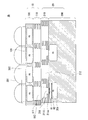
- FIG. 1 shows the configuration of a solid-state imaging device 1a according to the first embodiment of the present invention.
- FIG. 1 shows a cross section of the solid-state imaging device 1a.
- the solid-state imaging device 1 a includes a first substrate 10, a second substrate 20, a microlens 301, and a color filter 302. The first substrate 10 and the second substrate 20 are stacked.
- the dimensions of the parts constituting the solid-state imaging device 1a do not follow the dimensions shown in FIG.
- the dimension of the part which comprises the solid-state imaging device 1a may be arbitrary. In the present specification, dimensions in a specific direction in a specific region are described. When the dimensions of two specific regions are compared, the compared dimension may be the maximum dimension in a specific direction.
- the color filter 302 is disposed on the main surface of the first substrate 10 (the widest surface among the plurality of surfaces constituting the surface of the substrate), and the microlens 301 is disposed on the color filter 302.
- FIG. 1 there are a plurality of microlenses 301, but a symbol of one microlens 301 is shown as a representative.
- FIG. 1 there are a plurality of color filters 302, but a symbol of one color filter 302 is shown as a representative.
- the micro lens 301 forms an image of light that has passed through the imaging lens.
- the color filter 302 transmits light having a wavelength corresponding to a predetermined color.
- the first substrate 10 includes a first semiconductor layer 100 and a first wiring layer 110.
- the first semiconductor layer 100 and the first wiring layer 110 are formed in a direction (for example, substantially on the main surface) across the main surface of the first substrate 10 (the widest surface among a plurality of surfaces constituting the surface of the substrate). (Vertical direction). Further, the first semiconductor layer 100 and the first wiring layer 110 are in contact with each other.
- the first semiconductor layer 100 includes a first photoelectric conversion unit 101.
- the first semiconductor layer 100 is made of a material containing a semiconductor such as silicon (Si).
- the first photoelectric conversion unit 101 is made of a semiconductor material having an impurity concentration different from that of the semiconductor material forming the first semiconductor layer 100.
- the first semiconductor layer 100 has a first surface that is in contact with the first wiring layer 110.
- the second surface opposite to the first surface of the first semiconductor layer 100 is in contact with the color filter 302.
- the second surface of the first semiconductor layer 100 constitutes one of the main surfaces of the first substrate 10.
- the light transmitted through the microlens 301 and the color filter 302 is incident on the first semiconductor layer 100.
- the light incident on the first semiconductor layer 100 travels through the first semiconductor layer 100 and enters the first photoelectric conversion unit 101.
- the first photoelectric conversion unit 101 converts incident light into a signal.
- the first wiring layer 110 includes a first wiring 111 and a first interlayer insulating film 112.
- first wiring 111 there are a plurality of first wirings 111, but a symbol of one first wiring 111 is shown as a representative.
- the first wiring 111 is made of a conductive material (for example, a metal such as aluminum (Al) or copper (Cu)).
- the first wiring layer 110 has a first surface and a second surface. The first surface of the first wiring layer 110 is in contact with the second substrate 20. The second surface opposite to the first surface of the first wiring layer 110 is in contact with the first semiconductor layer 100. The first surface of the first wiring layer 110 constitutes one of the main surfaces of the first substrate 10.
- the first wiring 111 is a thin film on which a wiring pattern is formed.
- the first wiring 111 transmits a signal generated by the first photoelectric conversion unit 101 and other signals (power supply voltage, ground voltage, etc.). Only one layer of the first wiring 111 may be formed, or a plurality of layers of the first wiring 111 may be formed. In the example shown in FIG. 1, three layers of first wirings 111 are formed. The multiple layers of first wirings 111 are connected by vias (not shown).
- the portion other than the first wiring 111 is constituted by a first interlayer insulating film 112 formed of silicon dioxide (SiO 2) or the like.
- the second substrate 20 includes a second semiconductor layer 200 and a second wiring layer 210.
- the second semiconductor layer 200 and the second wiring layer 210 overlap in a direction crossing the main surface of the second substrate 20 (for example, a direction substantially perpendicular to the main surface). Further, the second semiconductor layer 200 and the second wiring layer 210 are in contact with each other.
- the second semiconductor layer 200 includes a second photoelectric conversion unit 201.
- the second semiconductor layer 200 is made of a material containing a semiconductor such as silicon (Si).
- the second photoelectric conversion unit 201 is made of a semiconductor material having an impurity concentration different from that of the semiconductor material forming the second semiconductor layer 200.
- a second photoelectric conversion unit 201 is formed in a region corresponding to the first photoelectric conversion unit 101. That is, the second photoelectric conversion unit 201 is formed at a position where light transmitted through the first photoelectric conversion unit 101 enters.
- the second semiconductor layer 200 has a first surface and a second surface.
- the first surface of the second semiconductor layer 200 is in contact with the second wiring layer 210.
- the second surface of the second semiconductor layer 200 constitutes one of the main surfaces of the second substrate 20.
- the second photoelectric conversion unit 201 is formed in the second semiconductor layer 200 in the vicinity of the first surface on which light is incident.
- the light that has passed through the first photoelectric conversion unit 101 passes through the first wiring layer 110 and enters the second wiring layer 210 of the second substrate 20.
- the light incident on the second wiring layer 210 passes through the second wiring layer 210 and enters the second semiconductor layer 200.
- the light incident on the second semiconductor layer 200 travels through the second semiconductor layer 200 and enters the second photoelectric conversion unit 201.
- the second photoelectric conversion unit 201 converts incident light into a signal.
- the second wiring layer 210 includes a second wiring 211 and a second interlayer insulating film 212.
- FIG. 1 there are a plurality of second wirings 211, but a symbol of one second wiring 211 is shown as a representative.
- the second wiring 211 is made of a conductive material (for example, a metal such as aluminum (Al) or copper (Cu)).
- the second wiring layer 210 has a first surface and a second surface. The first surface of the second wiring layer 210 is in contact with the first wiring layer 110. The second surface opposite to the first surface of the second wiring layer 210 is in contact with the second semiconductor layer 200. The first surface of the second wiring layer 210 constitutes one of the main surfaces of the second substrate 20.
- the second wiring 211 is a thin film on which a wiring pattern is formed.
- the second wiring 211 transmits the signal generated by the second photoelectric conversion unit 201 and other signals (power supply voltage, ground voltage, etc.). Only one layer of the second wiring 211 may be formed, or a plurality of layers of the second wiring 211 may be formed. In the example shown in FIG. 1, a three-layer second wiring 211 is formed. The plurality of layers of second wirings 211 are connected by vias not shown.
- the part other than the second wiring 211 is composed of a second interlayer insulating film 212 formed of silicon dioxide (SiO 2) or the like.
- the first substrate 10 and the second substrate 20 are stacked with the first wiring layer 110 of the first substrate 10 and the second wiring layer 210 of the second substrate 20 facing each other.
- the first substrate 10 and the second substrate 20 are electrically connected.
- the solid-state imaging device 1a has the following characteristics.
- the first substrate 10 includes a plurality of first photoelectric conversion units 101 on which the first light is incident.
- the plurality of first photoelectric conversion units 101 convert the first light into a signal.
- the second substrate 20 includes a second semiconductor layer 200 on which the second light is incident.
- the second semiconductor layer 200 includes a plurality of second photoelectric conversion units 201 on which the second light incident on the second semiconductor layer 200 enters.
- the plurality of second photoelectric conversion units 201 converts the second light into a signal.
- the second light is first light that has passed through the plurality of first photoelectric conversion units 101.
- the first dimension of the first range R1 is smaller than the second dimension of the second range R2.
- the first range R1 is the entire second photoelectric conversion unit 201.
- the first dimension is a dimension (maximum dimension) in the first range R1 in a direction parallel to the main surface of the second substrate 20.
- the second range R ⁇ b> 2 is a range in which the second light is incident on the second semiconductor layer 200.
- the second dimension is a dimension (maximum dimension) in the second range R2 in the direction parallel to the main surface of the second substrate 20.
- first ranges R1 there are a plurality of first ranges R1, but the reference numerals of one first range R1 are shown as representatives.
- second ranges R2 there are a plurality of second ranges R2, but the reference numerals of one second range R2 are shown as representatives.
- the solid-state imaging device 1a includes a plurality of microlenses 301 on which the first light is incident.
- the first light transmitted through the plurality of microlenses 301 enters the plurality of first photoelectric conversion units 101.
- the size of the second range R2 of the second semiconductor layer 200 includes the shape of the microlens 301, the refractive index and transmittance of the color filter 302 and the first semiconductor layer 100, and the third range R3 from the microlens 301. It can be calculated by the distance to For the calculation, an optical simulation using a ray tracing method or an FDTD (Finite-difference time-domain) method is used.
- the FDTD method is one method of electromagnetic field analysis.
- the first dimension in the first range R1 of the second photoelectric conversion unit 201 is the dimension of the second photoelectric conversion unit 201 in the direction parallel to the main surface of the second substrate 20. That is, the second light can enter the entire region of the second photoelectric conversion unit 201.
- the first dimension is smaller than the dimension of the first photoelectric conversion unit 101.
- the dimension of the first photoelectric conversion unit 101 is the dimension of the first photoelectric conversion unit 101 in a direction parallel to the main surface of the first substrate 10.
- the following conditions are satisfied.
- the plurality of first photoelectric conversion units 101 and the plurality of second photoelectric conversion units 201 are viewed in a direction perpendicular to the main surface of the first substrate 10 or the second substrate 20, the plurality of first photoelectric conversion units 101
- the respective centers of the photoelectric conversion units 101 and the respective centers of the plurality of second photoelectric conversion units 201 substantially coincide with each other.
- the plurality of second photoelectric conversion units 201 and the plurality of second ranges R2 are viewed in a direction perpendicular to the main surface of the second substrate 20, each of the plurality of second photoelectric conversion units 201 is displayed. And the centers of the plurality of second ranges R2 substantially coincide with each other.
- the first substrate 10 or the second substrate 20 has a wiring, that is, a first wiring 111 or a second wiring 211.
- a wiring that is, a first wiring 111 or a second wiring 211.
- FIG. 1 there is a positional shift between the first substrate 10 and the second substrate 20.
- the second substrate 20 is shifted to the right with respect to the first substrate 10.
- FIG. 1 when a plurality of first photoelectric conversion units 101 and a plurality of second photoelectric conversion units 201 are viewed in a direction perpendicular to the main surface of the first substrate 10 or the second substrate 20, The centers of the first photoelectric conversion units 101 do not coincide with the centers of the plurality of second photoelectric conversion units 201.
- the plurality of second photoelectric conversion units 201 and the plurality of second ranges R ⁇ b> 2 are viewed in the direction perpendicular to the main surface of the second substrate 20, the plurality of second photoelectric conversions are performed. Each center of the part 201 does not coincide with each center of the plurality of second ranges R2.
- the first range R1 of the second photoelectric conversion unit 201 is small. For this reason, when there is a positional shift between the first substrate 10 and the second substrate 20, the first range R1 and the second range R2 are viewed in a direction perpendicular to the main surface of the second substrate 20.
- the first range R1 is likely to be included within the second range R2. That is, the amount of light incident on the second photoelectric conversion unit 201 is less likely to depend on the amount of positional deviation between the first substrate 10 and the second substrate 20.
- the second wiring 211 transmits the second light transmitted through the first photoelectric conversion unit 101. It overlaps with the light path. For this reason, part of the second light is blocked by the second wiring 211.
- the first range R1 of the second photoelectric conversion unit 201 is smaller than the third dimension of the second range R2 of the second semiconductor layer 200. For this reason, the amount of the second light incident on the second photoelectric conversion unit 201 is unlikely to depend on the amount of the second light blocked by the second wiring 211.
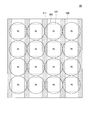
- FIG. 2 shows an arrangement of a plurality of first photoelectric conversion units 101.
- the first substrate 10 is shown as viewed in a direction perpendicular to the main surface of the first substrate 10.
- the surface of the first semiconductor layer 100 is shown.
- the first substrate 10 includes a plurality of first photoelectric conversion units 101 and a plurality of microlenses 301.
- reference numerals of one first photoelectric conversion unit 101 and one microlens 301 are shown as representatives.
- the plurality of first photoelectric conversion units 101 are arranged in a matrix.
- the plurality of microlenses 301 are arranged in a matrix.
- FIG. 2 shows the position of the first wiring 111.
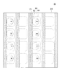
- FIG. 3 shows an arrangement of a plurality of second photoelectric conversion units 201.
- the second substrate 20 is shown as viewed in a direction perpendicular to the main surface of the second substrate 20.
- the surface of the second wiring layer 210 is shown.
- the second substrate 20 includes a plurality of second photoelectric conversion units 201 and a plurality of second wirings 211.
- reference numerals of one second photoelectric conversion unit 201 and one second wiring 211 are shown as representatives.
- the plurality of second photoelectric conversion units 201 are arranged in a matrix.
- FIG. 3 shows the positions of the first photoelectric conversion unit 101 and the second range R2 of the second semiconductor layer 200.
- the second photoelectric conversion unit 201 is shifted to the right with respect to the first photoelectric conversion unit 101. Further, the second photoelectric conversion unit 201 is shifted to the right with respect to the second range R2. However, the second photoelectric conversion unit 201 is inside the second range R2. When the positional deviation between the first substrate 10 and the second substrate 20 is small, the second photoelectric conversion unit 201 is within the second range R2 regardless of the amount of the deviation. For this reason, the amount of the second light incident on the second photoelectric conversion unit 201 is unlikely to depend on the amount of positional deviation between the first substrate 10 and the second substrate 20.
- the first photoelectric conversion unit 101 and the second photoelectric conversion unit 201 are rectangular.
- the second range R2 has a shape in which a part of the circle is missing.
- the shapes of the first photoelectric conversion unit 101, the second photoelectric conversion unit 201, and the second range R2 are not limited to the shapes shown in FIGS. Depending on these shapes and the amount of deviation, a part of the first range R1 of the second photoelectric conversion unit 201 may not fit in the second range R2. However, the reduction amount of the light incident on the first range R1 is small.
- the second dimension (diameter of the circular portion) in the second range R2 is R.
- the amount of positional deviation between the first substrate 10 and the second substrate 20 is D.
- the first dimension of the first range R1 is smaller than R-2D
- the first range R1 and the second range R2 are the first when viewed in the direction perpendicular to the main surface of the second substrate 20.
- One range R1 is likely to be included in the second range R2.
- the first dimension of the first range R1 of the second photoelectric conversion unit 201 is greater than zero.
- the dimension is determined so that the first dimension of the first range R1 is equal to or greater than R-2Dmax.
- Dmax is the maximum value of the allowable amount of positional deviation between the first substrate 10 and the second substrate 20.
- Dmax may be the same as the dimensions of the bumps.
- Dmax may be a value obtained from the measurement result of the amount of positional deviation between the first substrate 10 and the second substrate 20.
- the solid-state imaging device does not have a configuration corresponding to at least one of the first wiring layer 110, the second wiring layer 210, the microlens 301, and the color filter 302. Also good.
- the solid-state imaging device 1a including the first substrate 10 and the second substrate 20 is configured.
- the amount of light incident on the second photoelectric conversion unit 201 is less likely to depend on the amount of positional deviation between the first substrate 10 and the second substrate 20. As a result, it is possible to reduce variations in signals due to a positional shift between the first substrate 10 and the second substrate 20.
- FIG. 4 shows a configuration of a solid-state imaging device 1b according to the second embodiment of the present invention.
- FIG. 4 shows a cross section of the solid-state imaging device 1b.
- the solid-state imaging device 1 b includes a first substrate 10, a second substrate 20, a microlens 301, and a color filter 302. The first substrate 10 and the second substrate 20 are stacked.
- the second substrate 20 has a light shielding layer 211a in which a plurality of openings 2110 are formed.
- symbol of the one opening 2110 is shown as a representative.
- the light shielding layer 211a is disposed at a position that prevents the second light transmitted through the first photoelectric conversion unit 101 from proceeding.
- the light shielding layer 211 a reflects a part of the second light transmitted through the first photoelectric conversion unit 101.
- the second light except the light reflected by the light shielding layer 211a passes through the plurality of openings 2110.
- the second light that has passed through the plurality of openings 2110 is incident on the plurality of second photoelectric conversion units 201.
- the first dimension of the first range R1 is smaller than the second dimension of the second range R2.
- the first range R ⁇ b> 1 is a range in which the second light is incident on the second photoelectric conversion unit 201.
- the first dimension is a dimension (maximum dimension) in the first range R1 in a direction parallel to the main surface of the second substrate 20.
- the second range R2 is the entire second photoelectric conversion unit 201.
- the second dimension is a dimension (maximum dimension) in the second range R2 in the direction parallel to the main surface of the second substrate 20.
- each of the plurality of second photoelectric conversion units 201 and the plurality of openings 2110 are viewed in the direction perpendicular to the main surface of the second substrate 20, each of the plurality of second photoelectric conversion units 201 and the plurality of openings The center of the region where each of the portions 2110 overlaps substantially matches the center of each of the plurality of second photoelectric conversion units 201.
- the first substrate 10 is a back side illumination (BSI: Back Side Illumination) type imaging device.
- the first substrate 10 includes a first semiconductor layer 100 and a first wiring layer 110.
- the first semiconductor layer 100 includes a plurality of first photoelectric conversion units 101.
- the second substrate 20 is a front side illumination (FSI: Front Side Illumination) type imaging device.
- the second substrate 20 includes a second semiconductor layer 200 and a second wiring layer 210.
- the second semiconductor layer 200 includes a plurality of second photoelectric conversion units 201.
- the second wiring layer 210 includes a light shielding layer 211a.
- the light shielding layer 211 a is one layer of the second wiring 211.
- the light shielding layer 211 a is a layer of the second wiring 211 closest to the second photoelectric conversion unit 201.
- the light shielding layer 211 a may have a structure different from that of the second wiring 211.
- the first dimension of the first range R1 of the second photoelectric conversion unit 201 is smaller than the dimension of the opening 2110.
- the dimension of the opening 2110 is the dimension of the opening 2110 in the direction parallel to the main surface of the second substrate 20.
- the second dimension of the second range R2 of the second photoelectric conversion unit 201 is substantially equal to the dimension of the first photoelectric conversion unit 101 in the direction parallel to the main surface of the first substrate 10.
- the second dimension is larger than the dimension of the opening 2110.
- the first range R1 of the second photoelectric conversion unit 201 is small. For this reason, when there is a positional shift between the first substrate 10 and the second substrate 20, the first range R1 and the second range R2 are viewed in a direction perpendicular to the main surface of the second substrate 20.
- the first range R1 is likely to be included within the second range R2. That is, the amount of light incident on the second photoelectric conversion unit 201 is less likely to depend on the amount of positional deviation between the first substrate 10 and the second substrate 20.
- the arrangement of the plurality of first photoelectric conversion units 101 is the same as that shown in FIG.
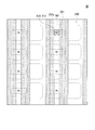
- FIG. 5 shows an arrangement of a plurality of second photoelectric conversion units 201.
- the second substrate 20 is shown as viewed in a direction perpendicular to the main surface of the second substrate 20.
- the surface of the second wiring layer 210 is shown.
- the second substrate 20 includes a plurality of second photoelectric conversion units 201, a plurality of second wirings 211, and a plurality of light shielding layers 211a.
- reference numerals of one second photoelectric conversion unit 201, one second wiring 211, and one light shielding layer 211a are shown as representatives.
- the plurality of second photoelectric conversion units 201 are arranged in a matrix. Further, in FIG. 5, the position of the first photoelectric conversion unit 101 is shown.
- the second photoelectric conversion unit 201 is shifted to the right with respect to the first photoelectric conversion unit 101.
- the region R ⁇ b> 10 where the opening 2110 included in the light shielding layer 211 a overlaps with the second photoelectric conversion unit 201 is inside the first photoelectric conversion unit 101.
- the region R10 is inside the first photoelectric conversion unit 101 regardless of the amount of the deviation. For this reason, the amount of the second light incident on the second photoelectric conversion unit 201 is unlikely to depend on the amount of positional deviation between the first substrate 10 and the second substrate 20.
- the first range R1 of the second photoelectric conversion unit 201 is the second range in the first embodiment. It is desirable to be included in the third range equivalent to the second range R2 of the semiconductor layer 200.
- the second dimension (diameter of the circular portion) in the second range R2 is R.
- the amount of positional deviation between the first substrate 10 and the second substrate 20 is D.
- the first dimension of the first range R1 of the second photoelectric conversion unit 201 is greater than zero.
- the dimensions are determined so that the first dimension of the first range R1 is equal to or greater than R-2Dmax.
- Dmax is the maximum value of the allowable amount of positional deviation between the first substrate 10 and the second substrate 20.
- Dmax may be the same as the dimensions of the bumps.
- Dmax may be a value obtained from the measurement result of the amount of positional deviation between the first substrate 10 and the second substrate 20.
- the dimension of the opening 2110 is determined so that the first dimension of the first range R1 becomes the determined dimension.
- the solid-state imaging device 1b including the first substrate 10 and the second substrate 20 is configured.
- the amount of light incident on the second photoelectric conversion unit 201 is less likely to depend on the amount of positional deviation between the first substrate 10 and the second substrate 20. As a result, it is possible to reduce variations in signals due to a positional shift between the first substrate 10 and the second substrate 20.
- FIG. 6 shows a configuration of a solid-state imaging device 1c according to the third embodiment of the present invention.
- FIG. 6 shows a cross section of the solid-state imaging device 1c.
- the solid-state imaging device 1 c includes a first substrate 10, a second substrate 20, a microlens 301, and a color filter 302. The first substrate 10 and the second substrate 20 are stacked.
- the first substrate 10 has a light shielding layer 111a in which a plurality of openings 1110 are formed.
- a symbol of one opening 1110 is shown as a representative.
- the light shielding layer 111 a is disposed at a position that prevents the second light transmitted through the first photoelectric conversion unit 101 from proceeding.
- the light shielding layer 111 a reflects a part of the second light transmitted through the first photoelectric conversion unit 101.
- the second light except the light reflected by the light shielding layer 111a passes through the plurality of openings 1110.
- the second light that has passed through the plurality of openings 1110 enters the plurality of second photoelectric conversion units 201.
- the first dimension of the first range R1 is smaller than the second dimension of the second range R2.
- the first range R ⁇ b> 1 is a range in which the second light is incident on the second photoelectric conversion unit 201.
- the first dimension is a dimension (maximum dimension) in the first range R1 in a direction parallel to the main surface of the second substrate 20.
- the second range R2 is the entire second photoelectric conversion unit 201.
- the second dimension is a dimension (maximum dimension) in the second range R2 in the direction parallel to the main surface of the second substrate 20.
- first ranges R1 Although there are a plurality of first ranges R1 in FIG. 5, a symbol of one first range R1 is shown as a representative. Further, in FIG. 5, there are a plurality of second ranges R2, but the reference numerals of one second range R2 are shown as representatives.
- each of the plurality of first photoelectric conversion units 101 and the plurality of openings 1110 are viewed in a direction perpendicular to the main surface of the first substrate 10, each of the plurality of first photoelectric conversion units 101 and the plurality of openings are provided.
- the center of the region where each of the parts 1110 overlaps substantially coincides with the center of each of the plurality of first photoelectric conversion units 101.
- the first substrate 10 is a back-illuminated image sensor.
- the first substrate 10 includes a first semiconductor layer 100 and a first wiring layer 110.
- the first semiconductor layer 100 includes a plurality of first photoelectric conversion units 101.
- the second substrate 20 is a surface irradiation type imaging device.
- the second substrate 20 includes a second semiconductor layer 200 and a second wiring layer 210.
- the second semiconductor layer 200 includes a plurality of second photoelectric conversion units 201.
- the first wiring layer 110 includes a light shielding layer 111a.
- the light shielding layer 111 a is one layer of the first wiring 111.
- the light shielding layer 111 a is a layer of the first wiring 111 that is closest to the second photoelectric conversion unit 201.
- the light shielding layer 111 a may have a structure different from that of the first wiring 111.
- the first dimension of the first range R1 of the second photoelectric conversion unit 201 is smaller than the dimension of the opening 1110.
- the dimension of the opening 1110 is the dimension of the opening 1110 in the direction parallel to the main surface of the first substrate 10.
- the second dimension of the second range R2 of the second photoelectric conversion unit 201 is substantially equal to the dimension of the first photoelectric conversion unit 101 in the direction parallel to the main surface of the first substrate 10.
- the second dimension is larger than the dimension of the opening 1110.
- the first range R1 of the second photoelectric conversion unit 201 is small. For this reason, when there is a positional shift between the first substrate 10 and the second substrate 20, the first range R1 and the second range R2 are viewed in a direction perpendicular to the main surface of the second substrate 20.
- the first range R1 is likely to be included within the second range R2. That is, the amount of light incident on the second photoelectric conversion unit 201 is less likely to depend on the amount of positional deviation between the first substrate 10 and the second substrate 20.
- FIG. 7 shows an arrangement of a plurality of first photoelectric conversion units 101.
- the first substrate 10 is shown as viewed in a direction perpendicular to the main surface of the first substrate 10.
- the surface of the first semiconductor layer 100 is shown.
- the first substrate 10 includes a plurality of first photoelectric conversion units 101 and a plurality of microlenses 301.
- the reference numerals of one first photoelectric conversion unit 101 and one microlens 301 are shown as representatives.
- the plurality of first photoelectric conversion units 101 are arranged in a matrix.
- the plurality of microlenses 301 are arranged in a matrix.
- FIG. 7 shows the positions of the first wiring 111 and the light shielding layer 111a.
- the arrangement of the plurality of second photoelectric conversion units 201 is the same as the arrangement shown in FIG. In the third embodiment, there is no light shielding layer 211a.
- the second dimension of the second photoelectric conversion unit 201 is L.
- the amount of positional deviation between the first substrate 10 and the second substrate 20 is D.
- the first dimension of the first range R1 is smaller than L-2D, when the second photoelectric conversion unit 201 is viewed in the direction perpendicular to the main surface of the second substrate 20, it depends on the amount of deviation. Therefore, the dimension of the first range R1 tends to be constant.
- the first dimension of the first range R1 of the second photoelectric conversion unit 201 is greater than zero.
- the dimension is determined so that the first dimension of the first range R1 is equal to or greater than L-2Dmax.
- Dmax is the maximum value of the allowable amount of positional deviation between the first substrate 10 and the second substrate 20.
- Dmax may be the same as the dimensions of the bumps.
- Dmax may be a value obtained from the measurement result of the amount of positional deviation between the first substrate 10 and the second substrate 20.
- the dimension of the opening 1110 is determined such that the first dimension of the first range R1 becomes the determined dimension.
- the solid-state imaging device 1c having the first substrate 10 and the second substrate 20 is configured.
- the amount of light incident on the second photoelectric conversion unit 201 is unlikely to depend on the amount of positional deviation between the first substrate 10 and the second substrate 20. As a result, it is possible to reduce variations in signals due to a positional shift between the first substrate 10 and the second substrate 20.
- FIG. 8 shows a configuration of an imaging apparatus 7 according to the fourth embodiment of the present invention.
- the imaging device 7 may be an electronic device having an imaging function.
- the imaging device 7 is any one of a digital camera, a digital video camera, an endoscope, and a microscope.
- the imaging device 7 includes a solid-state imaging device 1, a lens unit unit 2, an image signal processing device 3, a recording device 4, a camera control device 5, and a display device 6.
- the solid-state imaging device 1 is any one of the solid-state imaging device 1a of the first embodiment, the solid-state imaging device 1b of the second embodiment, and the solid-state imaging device 1c of the third embodiment.
- the lens unit 2 has a zoom lens and a focus lens.
- the lens unit 2 forms a subject image based on light from the subject on the light receiving surface of the solid-state imaging device 1.
- the light taken in through the lens unit 2 is imaged on the light receiving surface of the solid-state imaging device 1.
- the solid-state imaging device 1 converts the subject image formed on the light receiving surface into a signal such as an imaging signal and outputs the signal.
- the image signal processing device 3 performs a predetermined process on the signal output from the solid-state imaging device 1.
- the processing performed by the image signal processing device 3 includes conversion to image data, various corrections of the image data, and compression of the image data.
- the recording device 4 includes a semiconductor memory for recording or reading image data.
- the recording device 4 is detachable from the imaging device 7.
- the display device 6 displays an image based on the image data processed by the image signal processing device 3 or the image data read from the recording device 4.
- the camera control device 5 controls the entire imaging device 7.
- the operation of the camera control device 5 is defined by a program stored in a ROM built in the imaging device 7.
- the camera control device 5 reads out this program and performs various controls according to the contents defined by the program.
- the imaging device has a configuration corresponding to at least one of the lens unit unit 2, the image signal processing device 3, the recording device 4, the camera control device 5, and the display device 6. It does not have to be.
- the imaging device 7 having the solid-state imaging device 1 is configured.
- the solid-state imaging device 1 includes the first substrate 10 and the second substrate 20 in any one of the first to third embodiments. For this reason, it is possible to reduce variations in signals due to a positional shift between the first substrate 10 and the second substrate 20.
- the first dimension in the first range is smaller than the second dimension in the second range. For this reason, the amount of light incident on the second photoelectric conversion portion is unlikely to depend on the amount of positional deviation between the first substrate and the second substrate. As a result, it is possible to reduce variations in signals due to a positional shift between the first substrate and the second substrate.
- Solid-state imaging device 2 Lens unit 3 Image signal processing device 4 Recording device 5 Camera control device 6
Landscapes
- Physics & Mathematics (AREA)
- Spectroscopy & Molecular Physics (AREA)
- Engineering & Computer Science (AREA)
- Multimedia (AREA)
- Signal Processing (AREA)
- Solid State Image Pick-Up Elements (AREA)
- Transforming Light Signals Into Electric Signals (AREA)
Abstract
固体撮像装置は、第1の基板と、第2の基板とを有する。前記第1の基板は、第1の光が入射する複数の第1の光電変換部を有する。前記第2の基板は、第2の光が入射する第2の半導体層を有する。前記第2の半導体層は、前記第2の半導体層に入射した前記第2の光が入射する複数の第2の光電変換部を有する。前記第2の光は、前記複数の第1の光電変換部を透過した前記第1の光である。第1の範囲の第1の寸法は第2の範囲の第2の寸法よりも小さい。前記第1の範囲は、前記第2の光電変換部の全体である。前記第1の寸法は、前記第2の基板の主面に平行な方向の前記第1の範囲の寸法である。前記第2の範囲は、前記第2の半導体層において前記第2の光が入射する範囲である。前記第2の寸法は、前記第2の基板の主面に平行な方向の前記第2の範囲の寸法である。
Description
本発明は、複数の基板が積層された構造を有する固体撮像装置および撮像装置に関する。
複数の基板を有する固体撮像装置が開示されている。例えば、第1の基板と第2の基板とが積層された固体撮像装置が特許文献1に開示されている。特許文献1に開示された固体撮像装置では、複数の画素が第1の基板と第2の基板とに別々に配置されている。このため、撮像信号の解像度が向上する。
複数の基板を有する固体撮像装置の1つの例を説明する。図9は、固体撮像装置1000の構成を示している。図9では固体撮像装置1000の断面が示されている。図9に示すように、固体撮像装置1000は、第1の基板70と、第2の基板80と、マイクロレンズ901と、カラーフィルタ902とを有する。第1の基板70と、第2の基板80とは積層されている。
第1の基板70の主面(基板の表面を構成する複数の面のうち最も広い面)にカラーフィルタ902が配置され、カラーフィルタ902上にマイクロレンズ901が配置されている。図9では複数のマイクロレンズ901が存在するが、代表として1つのマイクロレンズ901の符号が示されている。また、図9では複数のカラーフィルタ902が存在するが、代表として1つのカラーフィルタ902の符号が示されている。
固体撮像装置1000の光学的前方に配置された撮像レンズを通過した、被写体からの光がマイクロレンズ901に入射する。マイクロレンズ901は、撮像レンズを透過した光を結像する。カラーフィルタ902は、所定の色に対応した波長の光を透過させる。
第1の基板70は、第1の半導体層700と、第1の配線層710とを有する。第1の半導体層700は、第1の光電変換部701を有する。図9では複数の第1の光電変換部701が存在するが、代表として1つの第1の光電変換部701の符号が示されている。第1の光電変換部701は、入射した光を信号に変換する。
第1の配線層710は、第1の配線711と、第1の層間絶縁膜712とを有する。図9では複数の第1の配線711が存在するが、代表として1つの第1の配線711の符号が示されている。
第1の配線711は、配線パターンが形成された薄膜である。第1の配線711は、第1の光電変換部701で生成された信号と、その他の信号(電源電圧、グランド電圧等)とを伝送する。図9に示す例では、3層の第1の配線711が形成されている。第1の配線層710において、第1の配線711以外の部分は、第1の層間絶縁膜712で構成されている。
第2の基板80は、第2の半導体層800と、第2の配線層810とを有する。第2の半導体層800は、第2の光電変換部801を有する。図9では複数の第2の光電変換部801が存在するが、代表として1つの第2の光電変換部801の符号が示されている。第2の光電変換部801は、入射した光を信号に変換する。
第2の配線層810は、第2の配線811と、第2の層間絶縁膜812とを有する。図9では複数の第2の配線811が存在するが、代表として1つの第2の配線811の符号が示されている。
第2の配線811は、配線パターンが形成された薄膜である。第2の配線811は、第2の光電変換部801で生成された信号と、その他の信号(電源電圧、グランド電圧等)とを伝送する。図9に示す例では、3層の第2の配線811が形成されている。第2の配線層810において、第2の配線811以外の部分は、第2の層間絶縁膜812で構成されている。
第1の基板70と第2の基板80とは、第1の基板70と第2の基板80との界面で電気的に接続されている。第1の光電変換部701が撮像信号を取得し、第2の光電変換部801が焦点検出用の信号を取得してもよい。
固体撮像装置1000の製造において、第1の基板70と第2の基板80とが接合されるとき、第1の基板70と第2の基板80との位置のずれが発生しうる。図10は、図9に示す固体撮像装置1000において第1の基板70と第2の基板80との位置のずれが発生している状態を示している。図10では、第2の基板80が第1の基板70に対して右方向にずれている。
マイクロレンズ901を透過した光は、カラーフィルタ902を透過する。カラーフィルタ902を透過した光は、第1の半導体層700に入射する。第1の半導体層700に入射した光は、第1の半導体層700内を進んで第1の光電変換部701に入射する。第1の光電変換部701を透過した光は、第1の配線層710と、第2の配線層810とを透過する。第2の配線層810を透過した光は第2の半導体層800の第2の範囲R102に入射する。第2の範囲R102に入射した光は第2の光電変換部801の第1の範囲R101に入射する。第2の基板80の主面に平行な方向の第2の光電変換部801の寸法は、第1の基板70の主面に平行な方向の第1の光電変換部701の寸法とほぼ等しい。
第1の範囲R101は、第2の光電変換部201において光が入射する範囲である。図10では複数の第1の範囲R101が存在するが、代表として1つの第1の範囲R101の符号が示されている。第2の範囲R102は、第2の半導体層800において光が入射する範囲である。図10では複数の第2の範囲R102が存在するが、代表として1つの第2の範囲R102の符号が示されている。
第1の基板70と第2の基板80との位置のずれがない場合、以下の条件が満たされる。複数の第1の光電変換部701と複数の第2の光電変換部801とを第1の基板70または第2の基板80の主面に垂直な方向に見た場合に、複数の第1の光電変換部701のそれぞれの中心と複数の第2の光電変換部801のそれぞれの中心とは、ほぼ一致する。また、複数の第2の光電変換部801と複数の第2の範囲R102とを第2の基板80の主面に垂直な方向に見た場合に、複数の第2の光電変換部801のそれぞれの中心と複数の第2の範囲R102のそれぞれの中心とは、ほぼ一致する。
図10では、第1の基板70と第2の基板80との位置のずれがある。図10では、複数の第1の光電変換部701と複数の第2の光電変換部801とを第1の基板70または第2の基板80の主面に垂直な方向に見た場合に、複数の第1の光電変換部701のそれぞれの中心と複数の第2の光電変換部801のそれぞれの中心とは、一致しない。また、図10では、複数の第2の光電変換部801と複数の第2の範囲R102とを第2の基板80の主面に垂直な方向に見た場合に、複数の第2の光電変換部801のそれぞれの中心と複数の第2の範囲R102のそれぞれの中心とは、一致しない。
第1の基板70と第2の基板80との位置のずれが小さい場合、第1の光電変換部701を透過した光の大部分は第2の光電変換部801に入射する。しかし、図10に示すように、第1の基板70と第2の基板80との位置のずれが大きい場合、第2の配線811が、第1の光電変換部701を透過した光の光路と重なる。このため、光の一部は第2の配線811によって遮られる。この結果、光の一部は第2の光電変換部801に入射しない。
図10では、第2の範囲R102の一部は、第2の光電変換部801が形成されている領域よりも外側(図10では左側)にある。このため、第2の配線811が存在しない場合でも、光の一部は第2の光電変換部801に入射しない。
したがって、第1の基板70と第2の基板80との位置のずれがある場合、第2の半導体層800に入射する光の一部は第2の光電変換部801に入射しない可能性がある。ずれの量に応じて、第2の光電変換部801に入射する光の量が異なる。半導体ウェハの面内でずれが均一ではない場合がある。つまり、ずれのばらつきが発生する場合がある。この場合、空間的に均一な光によって第2の光電変換部801において得られる信号がチップ毎に、または画素毎に異なる可能性がある。
本発明は、第1の基板と第2の基板との位置のずれによる信号のばらつきを低減することができる固体撮像装置および撮像装置を提供する。
本発明の第1の態様によれば、固体撮像装置は、第1の基板と、第2の基板とを有する。前記第1の基板は、第1の光が入射する複数の第1の光電変換部を有する。前記複数の第1の光電変換部は、前記第1の光を信号に変換する。前記第2の基板は、第2の光が入射する第2の半導体層を有する。前記第2の半導体層は、前記第2の半導体層に入射した前記第2の光が入射する複数の第2の光電変換部を有する。前記複数の第2の光電変換部は、前記第2の光を信号に変換する。前記第2の光は、前記複数の第1の光電変換部を透過した前記第1の光である。第1の範囲の第1の寸法は第2の範囲の第2の寸法よりも小さい。前記第1の範囲は、前記第2の光電変換部の全体である。前記第1の寸法は、前記第2の基板の主面に平行な方向の前記第1の範囲の寸法である。前記第2の範囲は、前記第2の半導体層において前記第2の光が入射する範囲である。前記第2の寸法は、前記第2の基板の主面に平行な方向の前記第2の範囲の寸法である。
本発明の第2の態様によれば、固体撮像装置は、第1の基板と、第2の基板とを有する。前記第1の基板は、第1の光が入射する複数の第1の光電変換部を有する。前記複数の第1の光電変換部は、前記第1の光を信号に変換する。前記第2の基板は、第2の光が入射する複数の第2の光電変換部を有する。前記複数の第2の光電変換部は、前記第2の光を信号に変換する。前記第2の光は、前記複数の第1の光電変換部を透過した前記第1の光である。前記第1の基板または前記第2の基板は、複数の開口部が形成された遮光層をさらに有する。前記遮光層は、前記第1の光電変換部を透過した前記第2の光の一部を反射する。前記遮光層によって反射された光を除く前記第2の光は前記複数の開口部を通過する。前記複数の開口部を通過した前記第2の光は前記複数の第2の光電変換部に入射する。第1の範囲の第1の寸法は第2の範囲の第2の寸法よりも小さい。前記第1の範囲は、前記第2の光電変換部において前記第2の光が入射する範囲である。前記第1の寸法は、前記第2の基板の主面に平行な方向の前記第1の範囲の寸法である。前記第2の範囲は、前記第2の光電変換部の全体である。前記第2の寸法は、前記第2の基板の主面に平行な方向の前記第2の範囲の寸法である。
本発明の第3の態様によれば、第1の態様または第2の態様において、前記第1の範囲と前記第2の範囲とを前記第2の基板の主面に垂直な方向に見た場合に、前記第1の範囲は前記第2の範囲の内部にあってもよい。
本発明の第4の態様によれば、第2の態様において、前記第2の基板は、前記遮光層を有してもよい。前記複数の第2の光電変換部と前記複数の開口部とを前記第2の基板の主面に垂直な方向に見た場合に、前記複数の第2の光電変換部のそれぞれと前記複数の開口部のそれぞれとが重なる領域の中心は前記複数の第2の光電変換部のそれぞれの中心とほぼ一致してもよい。
本発明の第5の態様によれば、第2の態様において、前記第1の基板は、前記遮光層を有してもよい。前記複数の第1の光電変換部と前記複数の開口部とを前記第1の基板の主面に垂直な方向に見た場合に、前記複数の第1の光電変換部のそれぞれと前記複数の開口部のそれぞれとが重なる領域の中心は前記複数の第1の光電変換部のそれぞれの中心とほぼ一致してもよい。
本発明の第6の態様によれば、第2の態様において、前記第2の基板は、表面照射型撮像素子であってもよい。前記第2の基板は、第2の半導体層と、第2の配線層とを有してもよい。前記第2の半導体層は前記複数の第2の光電変換部を有してもよい。前記第2の配線層は、前記遮光層を含んでもよい。
本発明の第7の態様によれば、第2の態様において、前記第1の基板は、裏面照射型撮像素子であってもよい。前記第1の基板は、第1の半導体層と、第1の配線層とを有してもよい。前記第1の半導体層は前記複数の第1の光電変換部を有してもよい。
本発明の第8の態様によれば、撮像装置は、前記固体撮像装置を有する。
上記の各態様によれば、第1の範囲の第1の寸法は第2の範囲の第2の寸法よりも小さい。このため、第2の光電変換部に入射する光の量が第1の基板と第2の基板との位置のずれの量に依存しにくい。この結果、第1の基板と第2の基板との位置のずれによる信号のばらつきを低減することができる。
図面を参照し、本発明の実施形態を説明する。
(第1の実施形態)
図1は、本発明の第1の実施形態の固体撮像装置1aの構成を示している。図1では固体撮像装置1aの断面が示されている。図1に示すように、固体撮像装置1aは、第1の基板10と、第2の基板20と、マイクロレンズ301と、カラーフィルタ302とを有する。第1の基板10と、第2の基板20とは積層されている。
図1は、本発明の第1の実施形態の固体撮像装置1aの構成を示している。図1では固体撮像装置1aの断面が示されている。図1に示すように、固体撮像装置1aは、第1の基板10と、第2の基板20と、マイクロレンズ301と、カラーフィルタ302とを有する。第1の基板10と、第2の基板20とは積層されている。
固体撮像装置1aを構成する部分の寸法は、図1に示される寸法に従うわけではない。固体撮像装置1aを構成する部分の寸法は任意であってよい。本明細書では、特定の領域における特定の方向の寸法が説明される。2つの特定の領域の寸法が比較される場合、比較される寸法は特定の方向の最大寸法であってよい。
第1の基板10の主面(基板の表面を構成する複数の面のうち最も広い面)にカラーフィルタ302が配置され、カラーフィルタ302上にマイクロレンズ301が配置されている。図1では複数のマイクロレンズ301が存在するが、代表として1つのマイクロレンズ301の符号が示されている。また、図1では複数のカラーフィルタ302が存在するが、代表として1つのカラーフィルタ302の符号が示されている。
固体撮像装置1aの光学的前方に配置された撮像レンズを通過した、被写体からの光がマイクロレンズ301に入射する。マイクロレンズ301は、撮像レンズを透過した光を結像する。カラーフィルタ302は、所定の色に対応した波長の光を透過させる。
第1の基板10は、第1の半導体層100と、第1の配線層110とを有する。第1の半導体層100と第1の配線層110とは、第1の基板10の主面(基板の表面を構成する複数の面のうち最も広い面)を横切る方向(例えば、主面にほぼ垂直な方向)に重なっている。また、第1の半導体層100と第1の配線層110とは互いに接触している。
第1の半導体層100は、第1の光電変換部101を有する。図1では複数の第1の光電変換部101が存在するが、代表として1つの第1の光電変換部101の符号が示されている。第1の半導体層100は、シリコン(Si)等の半導体を含む材料で構成されている。例えば、第1の光電変換部101は、第1の半導体層100を構成する半導体材料とは不純物濃度が異なる半導体材料で構成されている。第1の半導体層100は、第1の配線層110と接触している第1の面を有する。第1の半導体層100の第1の面と反対側の第2の面は、カラーフィルタ302と接触している。第1の半導体層100の第2の面は第1の基板10の主面の1つを構成する。
マイクロレンズ301とカラーフィルタ302とを透過した光は、第1の半導体層100に入射する。第1の半導体層100に入射した光は、第1の半導体層100内を進んで第1の光電変換部101に入射する。第1の光電変換部101は、入射した光を信号に変換する。
第1の配線層110は、第1の配線111と、第1の層間絶縁膜112とを有する。図1では複数の第1の配線111が存在するが、代表として1つの第1の配線111の符号が示されている。
第1の配線111は、導電性を有する材料(例えば、アルミニウム(Al)または銅(Cu)等の金属)で構成されている。第1の配線層110は、第1の面と第2の面とを有する。第1の配線層110の第1の面は第2の基板20と接触している。第1の配線層110の第1の面と反対側の第2の面は第1の半導体層100と接触している。第1の配線層110の第1の面は第1の基板10の主面の1つを構成する。
第1の配線111は、配線パターンが形成された薄膜である。第1の配線111は、第1の光電変換部101で生成された信号と、その他の信号(電源電圧、グランド電圧等)とを伝送する。1層のみの第1の配線111が形成されていてもよいし、複数層の第1の配線111が形成されていてもよい。図1に示す例では、3層の第1の配線111が形成されている。複数層の第1の配線111は、図示されていないビアによって接続されている。
第1の配線層110において、第1の配線111以外の部分は、二酸化珪素(SiO2)等で形成された第1の層間絶縁膜112で構成されている。
第2の基板20は、第2の半導体層200と、第2の配線層210とを有する。第2の半導体層200と第2の配線層210とは、第2の基板20の主面を横切る方向(例えば、主面にほぼ垂直な方向)に重なっている。また、第2の半導体層200と第2の配線層210とは互いに接触している。
第2の半導体層200は、第2の光電変換部201を有する。図1では複数の第2の光電変換部201が存在するが、代表として1つの第2の光電変換部201の符号が示されている。第2の半導体層200は、シリコン(Si)等の半導体を含む材料で構成されている。例えば、第2の光電変換部201は、第2の半導体層200を構成する半導体材料とは不純物濃度が異なる半導体材料で構成されている。第1の光電変換部101に対応する領域に第2の光電変換部201が形成されている。つまり、第2の光電変換部201は、第1の光電変換部101を透過した光が入射する位置に形成されている。第2の半導体層200は、第1の面と第2の面とを有する。第2の半導体層200の第1の面は第2の配線層210と接触している。第2の半導体層200の第2の面は第2の基板20の主面の1つを構成する。第2の光電変換部201は、第2の半導体層200において、光が入射する第1の面の近傍に形成されている。
第1の光電変換部101を透過した光は、第1の配線層110を透過し、第2の基板20の第2の配線層210に入射する。第2の配線層210に入射した光は、第2の配線層210を透過し、第2の半導体層200に入射する。第2の半導体層200に入射した光は、第2の半導体層200内を進んで第2の光電変換部201に入射する。第2の光電変換部201は、入射した光を信号に変換する。
第2の配線層210は、第2の配線211と、第2の層間絶縁膜212とを有する。図1では複数の第2の配線211が存在するが、代表として1つの第2の配線211の符号が示されている。
第2の配線211は、導電性を有する材料(例えば、アルミニウム(Al)または銅(Cu)等の金属)で構成されている。第2の配線層210は、第1の面と第2の面とを有する。第2の配線層210の第1の面は第1の配線層110と接触している。第2の配線層210の第1の面と反対側の第2の面は第2の半導体層200と接触している。第2の配線層210の第1の面は第2の基板20の主面の1つを構成する。
第2の配線211は、配線パターンが形成された薄膜である。第2の配線211は、第2の光電変換部201で生成された信号と、その他の信号(電源電圧、グランド電圧等)とを伝送する。1層のみの第2の配線211が形成されていてもよいし、複数層の第2の配線211が形成されていてもよい。図1に示す例では、3層の第2の配線211が形成されている。複数層の第2の配線211は、図示されていないビアによって接続されている。
第2の配線層210において、第2の配線211以外の部分は、二酸化珪素(SiO2)等で形成された第2の層間絶縁膜212で構成されている。
第1の基板10と第2の基板20とは、第1の基板10の第1の配線層110と第2の基板20の第2の配線層210とが向かい合った状態で積層されている。第1の基板10と第2の基板20とは、電気的に接続されている。
固体撮像装置1aは、以下の特徴を有する。第1の基板10は、第1の光が入射する複数の第1の光電変換部101を有する。複数の第1の光電変換部101は、第1の光を信号に変換する。第2の基板20は、第2の光が入射する第2の半導体層200を有する。第2の半導体層200は、第2の半導体層200に入射した第2の光が入射する複数の第2の光電変換部201を有する。複数の第2の光電変換部201は、第2の光を信号に変換する。第2の光は、複数の第1の光電変換部101を透過した第1の光である。
第1の範囲R1の第1の寸法は第2の範囲R2の第2の寸法よりも小さい。第1の範囲R1は、第2の光電変換部201の全体である。第1の寸法は、第2の基板20の主面に平行な方向の第1の範囲R1の寸法(最大寸法)である。第2の範囲R2は、第2の半導体層200において第2の光が入射する範囲である。第2の寸法は、第2の基板20の主面に平行な方向の第2の範囲R2の寸法(最大寸法)である。第1の範囲R1と第2の範囲R2とを第2の基板20の主面に垂直な方向に見た場合に、第1の範囲R1は第2の範囲R2の内部にあることが望ましい。図1では複数の第1の範囲R1が存在するが、代表として1つの第1の範囲R1の符号が示されている。また、図1では複数の第2の範囲R2が存在するが、代表として1つの第2の範囲R2の符号が示されている。
固体撮像装置1aは、第1の光が入射する複数のマイクロレンズ301を有する。複数のマイクロレンズ301を透過した第1の光は複数の第1の光電変換部101に入射する。
第2の半導体層200の第2の範囲R2の大きさは、マイクロレンズ301の形状、カラーフィルタ302と第1の半導体層100との屈折率および透過率、マイクロレンズ301から第3の範囲R3までの距離等により算出できる。また、その算出には、光線追跡法またはFDTD(Finite-difference time-domain)法を用いた光学シミュレーションが用いられる。FDTD法は、電磁場解析の一手法である。
第2の光電変換部201の第1の範囲R1の第1の寸法は、第2の基板20の主面に平行な方向の第2の光電変換部201の寸法である。つまり、第2の光電変換部201の領域全体に第2の光が入射することが可能である。第1の寸法は第1の光電変換部101の寸法よりも小さい。第1の光電変換部101の寸法は、第1の基板10の主面に平行な方向の第1の光電変換部101の寸法である。
第1の基板10と第2の基板20との位置のずれがない場合、以下の条件が満たされる。複数の第1の光電変換部101と複数の第2の光電変換部201とを第1の基板10または第2の基板20の主面に垂直な方向に見た場合に、複数の第1の光電変換部101のそれぞれの中心と複数の第2の光電変換部201のそれぞれの中心とは、ほぼ一致する。また、複数の第2の光電変換部201と複数の第2の範囲R2とを第2の基板20の主面に垂直な方向に見た場合に、複数の第2の光電変換部201のそれぞれの中心と複数の第2の範囲R2のそれぞれの中心とは、ほぼ一致する。
第1の基板10または第2の基板20は、配線、すなわち第1の配線111または第2の配線211を有する。第1の基板10と第2の基板20との位置のずれがない場合、第1の配線111と第2の配線211とは、第1の光電変換部101を透過した第2の光の進行を妨げない位置に配置されている。
図1では、第1の基板10と第2の基板20との位置のずれが発生している。図1では、第2の基板20が第1の基板10に対して右方向にずれている。図1では、複数の第1の光電変換部101と複数の第2の光電変換部201とを第1の基板10または第2の基板20の主面に垂直な方向に見た場合に、複数の第1の光電変換部101のそれぞれの中心と複数の第2の光電変換部201のそれぞれの中心とは、一致しない。また、図1では、複数の第2の光電変換部201と複数の第2の範囲R2とを第2の基板20の主面に垂直な方向に見た場合に、複数の第2の光電変換部201のそれぞれの中心と複数の第2の範囲R2のそれぞれの中心とは、一致しない。
第2の半導体層200の第2の範囲R2と比較して、第2の光電変換部201の第1の範囲R1は小さい。このため、第1の基板10と第2の基板20との位置のずれがある場合、第1の範囲R1と第2の範囲R2とを第2の基板20の主面に垂直な方向に見たときに第1の範囲R1が第2の範囲R2の内部に含まれやすい。つまり、第2の光電変換部201に入射する光の量が第1の基板10と第2の基板20との位置のずれの量に依存しにくい。
第1の基板10と第2の基板20との位置のずれが小さい場合、第1の光電変換部101を透過した第2の光の大部分は第2の光電変換部201に入射する。しかし、図1に示すように、第1の基板10と第2の基板20との位置のずれが大きい場合、第2の配線211が、第1の光電変換部101を透過した第2の光の光路と重なる。このため、第2の光の一部は第2の配線211によって遮られる。第2の光電変換部201の第1の範囲R1は、第2の半導体層200の第2の範囲R2の第3の寸法よりも小さい。このため、第2の光電変換部201に入射する第2の光の量は、第2の配線211によって遮られる第2の光の量に依存しにくい。
図2は、複数の第1の光電変換部101の配列を示している。図2では、第1の基板10の主面に垂直な方向に見た第1の基板10が示されている。図2では、第1の半導体層100の表面が示されている。図2に示すように、第1の基板10は、複数の第1の光電変換部101と複数のマイクロレンズ301とを有する。図2では代表として1つの第1の光電変換部101と1つのマイクロレンズ301との符号が示されている。複数の第1の光電変換部101は行列状に配置されている。また、複数のマイクロレンズ301は行列状に配置されている。また、図2では、第1の配線111の位置が示されている。
図3は、複数の第2の光電変換部201の配列を示している。図3では、第2の基板20の主面に垂直な方向に見た第2の基板20が示されている。図3では、第2の配線層210の表面が示されている。図3に示すように、第2の基板20は、複数の第2の光電変換部201と複数の第2の配線211とを有する。図3では代表として1つの第2の光電変換部201と1つの第2の配線211との符号が示されている。複数の第2の光電変換部201は行列状に配置されている。また、図3では、第1の光電変換部101と第2の半導体層200の第2の範囲R2との位置が示されている。
第1の基板10と第2の基板20との位置のずれがある。このため、図3に示すように、第2の光電変換部201は第1の光電変換部101に対して右方向にずれている。また、第2の光電変換部201は第2の範囲R2に対して右方向にずれている。しかし、第2の光電変換部201は第2の範囲R2の内部にある。第1の基板10と第2の基板20との位置のずれが小さい場合、そのずれの量によらず、第2の光電変換部201は第2の範囲R2の内部にある。このため、第2の光電変換部201に入射する第2の光の量が第1の基板10と第2の基板20との位置のずれの量に依存しにくい。
図2と図3とに示すように、第1の光電変換部101と第2の光電変換部201とは矩形状である。また、第2の範囲R2は、円の一部が欠けた形状である。第1の光電変換部101と、第2の光電変換部201と、第2の範囲R2との形状は、図2と図3とに示す形状に限らない。これらの形状とずれの量とによっては、第2の光電変換部201の第1の範囲R1の一部が第2の範囲R2に収まらない可能性がある。しかし、第1の範囲R1に入射する光の減少量は小さい。
例えば、第2の範囲R2の第2の寸法(円状の部分の直径)はRである。例えば、第1の基板10と第2の基板20との位置のずれの量はDである。第1の範囲R1の第1の寸法がR-2Dよりも小さい場合、第1の範囲R1と第2の範囲R2とを第2の基板20の主面に垂直な方向に見たときに第1の範囲R1が第2の範囲R2の内部に含まれやすい。
第2の光電変換部201の第1の範囲R1の第1の寸法は0よりも大きい。例えば、固体撮像装置1aの設計時に、第1の範囲R1の第1の寸法がR-2Dmax以上となるように、その寸法が決定される。Dmaxは、第1の基板10と第2の基板20との位置のずれの許容量の最大値である。例えば、第1の基板10と第2の基板20とがバンプによって電気的に接続される場合、Dmaxはバンプの寸法と同じであってもよい。あるいは、Dmaxは、第1の基板10と第2の基板20との位置のずれの量の測定結果から求められた値であってもよい。
本発明の各態様の固体撮像装置は、第1の配線層110と、第2の配線層210と、マイクロレンズ301と、カラーフィルタ302との少なくとも1つに対応する構成を有していなくてもよい。
第1の実施形態によれば、第1の基板10と、第2の基板20とを有する固体撮像装置1aが構成される。
第1の実施形態では、第2の光電変換部201に入射する光の量が第1の基板10と第2の基板20との位置のずれの量に依存しにくい。この結果、第1の基板10と第2の基板20との位置のずれによる信号のばらつきを低減することができる。
(第2の実施形態)
図4は、本発明の第2の実施形態の固体撮像装置1bの構成を示している。図4では固体撮像装置1bの断面が示されている。図4に示すように、固体撮像装置1bは、第1の基板10と、第2の基板20と、マイクロレンズ301と、カラーフィルタ302とを有する。第1の基板10と、第2の基板20とは積層されている。
図4は、本発明の第2の実施形態の固体撮像装置1bの構成を示している。図4では固体撮像装置1bの断面が示されている。図4に示すように、固体撮像装置1bは、第1の基板10と、第2の基板20と、マイクロレンズ301と、カラーフィルタ302とを有する。第1の基板10と、第2の基板20とは積層されている。
図4に示す構成について、図1に示す構成と異なる点を説明する。
第2の基板20は、複数の開口部2110が形成された遮光層211aを有する。図4では代表として1つの開口部2110の符号が示されている。遮光層211aは、第1の光電変換部101を透過した第2の光の進行を妨げる位置に配置されている。遮光層211aは、第1の光電変換部101を透過した第2の光の一部を反射する。遮光層211aによって反射された光を除く第2の光は複数の開口部2110を通過する。複数の開口部2110を通過した第2の光は複数の第2の光電変換部201に入射する。
第1の範囲R1の第1の寸法は第2の範囲R2の第2の寸法よりも小さい。第1の範囲R1は、第2の光電変換部201において第2の光が入射する範囲である。第1の寸法は、第2の基板20の主面に平行な方向の第1の範囲R1の寸法(最大寸法)である。第2の範囲R2は、第2の光電変換部201の全体である。第2の寸法は、第2の基板20の主面に平行な方向の第2の範囲R2の寸法(最大寸法)である。第1の範囲R1と第2の範囲R2とを第2の基板20の主面に垂直な方向に見た場合に、第1の範囲R1は第2の範囲R2の内部にあることが望ましい。図4では複数の第1の範囲R1が存在するが、代表として1つの第1の範囲R1の符号が示されている。また、図4では複数の第2の範囲R2が存在するが、代表として1つの第2の範囲R2の符号が示されている。
複数の第2の光電変換部201と複数の開口部2110とを第2の基板20の主面に垂直な方向に見た場合に、複数の第2の光電変換部201のそれぞれと複数の開口部2110のそれぞれとが重なる領域の中心は複数の第2の光電変換部201のそれぞれの中心とほぼ一致する。
第1の基板10は、裏面照射(BSI:Back Side Illumination)型撮像素子である。第1の基板10は、第1の半導体層100と、第1の配線層110とを有する。第1の半導体層100は複数の第1の光電変換部101を有する。第2の基板20は、表面照射(FSI:Front Side Illumination)型撮像素子である。第2の基板20は、第2の半導体層200と、第2の配線層210とを有する。第2の半導体層200は複数の第2の光電変換部201を有する。第2の配線層210は、遮光層211aを含む。
図4では、遮光層211aは第2の配線211の1つの層である。図4では、遮光層211aは、第2の光電変換部201に最も近い第2の配線211の層である。遮光層211aは、第2の配線211とは別の構造であってもよい。
第2の光電変換部201の第1の範囲R1の第1の寸法は開口部2110の寸法よりも小さい。開口部2110の寸法は、第2の基板20の主面に平行な方向の開口部2110の寸法である。
第2の光電変換部201の第2の範囲R2の第2の寸法は、第1の基板10の主面に平行な方向の第1の光電変換部101の寸法とほぼ等しい。第2の寸法は、開口部2110の寸法よりも大きい。
上記以外の点については、図4に示す構成は図1に示す構成と同様である。
第2の光電変換部201の第2の範囲R2と比較して、第2の光電変換部201の第1の範囲R1は小さい。このため、第1の基板10と第2の基板20との位置のずれがある場合、第1の範囲R1と第2の範囲R2とを第2の基板20の主面に垂直な方向に見たときに第1の範囲R1が第2の範囲R2の内部に含まれやすい。つまり、第2の光電変換部201に入射する光の量が第1の基板10と第2の基板20との位置のずれの量に依存しにくい。
複数の第1の光電変換部101の配列は、図2に示す配列と同様である。
図5は、複数の第2の光電変換部201の配列を示している。図5では、第2の基板20の主面に垂直な方向に見た第2の基板20が示されている。図5では、第2の配線層210の表面が示されている。図5に示すように、第2の基板20は、複数の第2の光電変換部201と、複数の第2の配線211と、複数の遮光層211aとを有する。図5では代表として1つの第2の光電変換部201と、1つの第2の配線211と、1つの遮光層211aとの符号が示されている。複数の第2の光電変換部201は行列状に配置されている。また、図5では、第1の光電変換部101の位置が示されている。
複数の第2の光電変換部201のそれぞれと複数の開口部2110のそれぞれとが重なる領域R10の中心は複数の第2の光電変換部201のそれぞれの中心とほぼ一致する。図5では代表として1つの領域R10の符号が示されている。
第1の基板10と第2の基板20との位置のずれがある。このため、図5に示すように、第2の光電変換部201は第1の光電変換部101に対して右方向にずれている。しかし、遮光層211aが有する開口部2110と第2の光電変換部201とが重なる領域R10は第1の光電変換部101の内部にある。第1の基板10と第2の基板20との位置のずれが小さい場合、そのずれの量によらず、領域R10は第1の光電変換部101の内部にある。このため、第2の光電変換部201に入射する第2の光の量が第1の基板10と第2の基板20との位置のずれの量に依存しにくい。
第2の光電変換部201を第2の基板20の主面に垂直な方向に見た場合に、第2の光電変換部201の第1の範囲R1が、第1の実施形態における第2の半導体層200の第2の範囲R2と同等の第3の範囲に含まれることが望ましい。例えば、第2の範囲R2の第2の寸法(円状の部分の直径)はRである。例えば、第1の基板10と第2の基板20との位置のずれの量はDである。第1の範囲R1の第1の寸法がR-2Dよりも小さい場合、第2の光電変換部201を第2の基板20の主面に垂直な方向に見たときに第1の範囲R1が第2の範囲R2の内部に含まれやすい。
第2の光電変換部201の第1の範囲R1の第1の寸法は0よりも大きい。例えば、固体撮像装置1bの設計時に、第1の範囲R1の第1の寸法がR-2Dmax以上となるように、その寸法が決定される。Dmaxは、第1の基板10と第2の基板20との位置のずれの許容量の最大値である。例えば、第1の基板10と第2の基板20とがバンプによって電気的に接続される場合、Dmaxはバンプの寸法と同じであってもよい。あるいは、Dmaxは、第1の基板10と第2の基板20との位置のずれの量の測定結果から求められた値であってもよい。第1の範囲R1の第1の寸法が決定された寸法になるように、開口部2110の寸法が決定される。
第2の実施形態によれば、第1の基板10と、第2の基板20とを有する固体撮像装置1bが構成される。
第2の実施形態では、第2の光電変換部201に入射する光の量が第1の基板10と第2の基板20との位置のずれの量に依存しにくい。この結果、第1の基板10と第2の基板20との位置のずれによる信号のばらつきを低減することができる。
(第3の実施形態)
図6は、本発明の第3の実施形態の固体撮像装置1cの構成を示している。図6では固体撮像装置1cの断面が示されている。図6に示すように、固体撮像装置1cは、第1の基板10と、第2の基板20と、マイクロレンズ301と、カラーフィルタ302とを有する。第1の基板10と、第2の基板20とは積層されている。
図6は、本発明の第3の実施形態の固体撮像装置1cの構成を示している。図6では固体撮像装置1cの断面が示されている。図6に示すように、固体撮像装置1cは、第1の基板10と、第2の基板20と、マイクロレンズ301と、カラーフィルタ302とを有する。第1の基板10と、第2の基板20とは積層されている。
図6に示す構成について、図1に示す構成と異なる点を説明する。
第1の基板10は、複数の開口部1110が形成された遮光層111aを有する。図6では代表として1つの開口部1110の符号が示されている。遮光層111aは、第1の光電変換部101を透過した第2の光の進行を妨げる位置に配置されている。遮光層111aは、第1の光電変換部101を透過した第2の光の一部を反射する。遮光層111aによって反射された光を除く第2の光は複数の開口部1110を通過する。複数の開口部1110を通過した第2の光は複数の第2の光電変換部201に入射する。
第1の範囲R1の第1の寸法は第2の範囲R2の第2の寸法よりも小さい。第1の範囲R1は、第2の光電変換部201において第2の光が入射する範囲である。第1の寸法は、第2の基板20の主面に平行な方向の第1の範囲R1の寸法(最大寸法)である。第2の範囲R2は、第2の光電変換部201の全体である。第2の寸法は、第2の基板20の主面に平行な方向の第2の範囲R2の寸法(最大寸法)である。第1の範囲R1と第2の範囲R2とを第2の基板20の主面に垂直な方向に見た場合に、第1の範囲R1は第2の範囲R2の内部にあることが望ましい。図5では複数の第1の範囲R1が存在するが、代表として1つの第1の範囲R1の符号が示されている。また、図5では複数の第2の範囲R2が存在するが、代表として1つの第2の範囲R2の符号が示されている。
複数の第1の光電変換部101と複数の開口部1110とを第1の基板10の主面に垂直な方向に見た場合に、複数の第1の光電変換部101のそれぞれと複数の開口部1110のそれぞれとが重なる領域の中心は複数の第1の光電変換部101のそれぞれの中心とほぼ一致する。
第1の基板10は、裏面照射型撮像素子である。第1の基板10は、第1の半導体層100と、第1の配線層110とを有する。第1の半導体層100は複数の第1の光電変換部101を有する。第2の基板20は、表面照射型撮像素子である。第2の基板20は、第2の半導体層200と、第2の配線層210とを有する。第2の半導体層200は複数の第2の光電変換部201を有する。第1の配線層110は、遮光層111aを含む。
図6では、遮光層111aは第1の配線111の1つの層である。図6では、遮光層111aは、第2の光電変換部201に最も近い第1の配線111の層である。遮光層111aは、第1の配線111とは別の構造であってもよい。
第2の光電変換部201の第1の範囲R1の第1の寸法は開口部1110の寸法よりも小さい。開口部1110の寸法は、第1の基板10の主面に平行な方向の開口部1110の寸法である。
第2の光電変換部201の第2の範囲R2の第2の寸法は、第1の基板10の主面に平行な方向の第1の光電変換部101の寸法とほぼ等しい。第2の寸法は、開口部1110の寸法よりも大きい。
上記以外の点については、図6に示す構成は図1に示す構成と同様である。
第2の光電変換部201の第2の範囲R2と比較して、第2の光電変換部201の第1の範囲R1は小さい。このため、第1の基板10と第2の基板20との位置のずれがある場合、第1の範囲R1と第2の範囲R2とを第2の基板20の主面に垂直な方向に見たときに第1の範囲R1が第2の範囲R2の内部に含まれやすい。つまり、第2の光電変換部201に入射する光の量が第1の基板10と第2の基板20との位置のずれの量に依存しにくい。
図7は、複数の第1の光電変換部101の配列を示している。図7では、第1の基板10の主面に垂直な方向に見た第1の基板10が示されている。図7では、第1の半導体層100の表面が示されている。図7に示すように、第1の基板10は、複数の第1の光電変換部101と複数のマイクロレンズ301とを有する。図7では代表として1つの第1の光電変換部101と1つのマイクロレンズ301との符号が示されている。複数の第1の光電変換部101は行列状に配置されている。また、複数のマイクロレンズ301は行列状に配置されている。また、図7では、第1の配線111と遮光層111aとの位置が示されている。
複数の第1の光電変換部101のそれぞれと複数の開口部1110のそれぞれとが重なる領域R11の中心は複数の第1の光電変換部101のそれぞれの中心とほぼ一致する。図7では代表として1つの領域R11の符号が示されている。
複数の第2の光電変換部201の配列は、図5に示す配列と同様である。第3の実施形態では、遮光層211aはない。
例えば、第2の光電変換部201の第2の寸法はLである。例えば、第1の基板10と第2の基板20との位置のずれの量はDである。第1の範囲R1の第1の寸法がL-2Dよりも小さい場合、第2の光電変換部201を第2の基板20の主面に垂直な方向に見たときに、ずれの量によらず、第1の範囲R1の寸法が一定になりやすい。
第2の光電変換部201の第1の範囲R1の第1の寸法は0よりも大きい。例えば、固体撮像装置1cの設計時に、第1の範囲R1の第1の寸法がL-2Dmax以上となるように、その寸法が決定される。Dmaxは、第1の基板10と第2の基板20との位置のずれの許容量の最大値である。例えば、第1の基板10と第2の基板20とがバンプによって電気的に接続される場合、Dmaxはバンプの寸法と同じであってもよい。あるいは、Dmaxは、第1の基板10と第2の基板20との位置のずれの量の測定結果から求められた値であってもよい。第1の範囲R1の第1の寸法が決定された寸法になるように、開口部1110の寸法が決定される。
第3の実施形態によれば、第1の基板10と、第2の基板20とを有する固体撮像装置1cが構成される。
第3の実施形態では、第2の光電変換部201に入射する光の量が第1の基板10と第2の基板20との位置のずれの量に依存しにくい。この結果、第1の基板10と第2の基板20との位置のずれによる信号のばらつきを低減することができる。
(第4の実施形態)
図8は、本発明の第4の実施形態の撮像装置7の構成を示している。撮像装置7は、撮像機能を有する電子機器であればよい。例えば、撮像装置7は、デジタルカメラと、デジタルビデオカメラと、内視鏡と、顕微鏡とのいずれか1つである。図8に示すように、撮像装置7は、固体撮像装置1と、レンズユニット部2と、画像信号処理装置3と、記録装置4と、カメラ制御装置5と、表示装置6とを有する。
図8は、本発明の第4の実施形態の撮像装置7の構成を示している。撮像装置7は、撮像機能を有する電子機器であればよい。例えば、撮像装置7は、デジタルカメラと、デジタルビデオカメラと、内視鏡と、顕微鏡とのいずれか1つである。図8に示すように、撮像装置7は、固体撮像装置1と、レンズユニット部2と、画像信号処理装置3と、記録装置4と、カメラ制御装置5と、表示装置6とを有する。
固体撮像装置1は、第1の実施形態の固体撮像装置1aと、第2の実施形態の固体撮像装置1bと、第3の実施形態の固体撮像装置1cとのいずれか1つである。レンズユニット部2は、ズームレンズとフォーカスレンズとを有する。レンズユニット部2は、被写体からの光に基づく被写体像を固体撮像装置1の受光面に形成する。レンズユニット部2を介して取り込まれた光は固体撮像装置1の受光面に結像される。固体撮像装置1は、受光面に結像された被写体像を撮像信号等の信号に変換し、その信号を出力する。
画像信号処理装置3は、固体撮像装置1から出力された信号に対して、予め定められた処理を行う。画像信号処理装置3によって行われる処理は、画像データへの変換、画像データの各種の補正、および画像データの圧縮などである。
記録装置4は、画像データの記録または読み出しを行うための半導体メモリなどを有する。記録装置4は、撮像装置7に対して着脱可能である。表示装置6は、画像信号処理装置3によって処理された画像データ、または記録装置4から読み出された画像データに基づく画像を表示する。
カメラ制御装置5は、撮像装置7全体の制御を行う。カメラ制御装置5の動作は、撮像装置7に内蔵されたROMに格納されているプログラムに規定されている。カメラ制御装置5は、このプログラムを読み出して、プログラムが規定する内容に従って、各種の制御を行う。
本発明の各態様の撮像装置は、レンズユニット部2と、画像信号処理装置3と、記録装置4と、カメラ制御装置5と、表示装置6との少なくとも1つに対応する構成を有していなくてもよい。
第4の実施形態によれば、固体撮像装置1を有する撮像装置7が構成される。固体撮像装置1は、第1から第3の実施形態のいずれか1つにおける第1の基板10と第2の基板20とを有する。このため、第1の基板10と第2の基板20との位置のずれによる信号のばらつきを低減することができる。
以上、図面を参照して本発明の実施形態について詳述してきたが、具体的な構成は上記の実施形態に限られるものではなく、本発明の要旨を逸脱しない範囲の設計変更等も含まれる。
本発明の各実施形態によれば、第1の範囲の第1の寸法は第2の範囲の第2の寸法よりも小さい。このため、第2の光電変換部に入射する光の量が第1の基板と第2の基板との位置のずれの量に依存しにくい。この結果、第1の基板と第2の基板との位置のずれによる信号のばらつきを低減することができる。
1,1a,1b,1c,1000 固体撮像装置
2 レンズユニット部
3 画像信号処理装置
4 記録装置
5 カメラ制御装置
6 表示装置
7 撮像装置
10,70 第1の基板
20,80 第2の基板
100,700 第1の半導体層
101,701 第1の光電変換部
110,710 第1の配線層
111,711 第1の配線
111a,211a 遮光層
112,712 第1の層間絶縁膜
200,800 第2の半導体層
201,801 第2の光電変換部
210,810 第2の配線層
211,811 第2の配線
212,812 第2の層間絶縁膜
301,901 マイクロレンズ
302,902 カラーフィルタ
1110,2110 開口部
2 レンズユニット部
3 画像信号処理装置
4 記録装置
5 カメラ制御装置
6 表示装置
7 撮像装置
10,70 第1の基板
20,80 第2の基板
100,700 第1の半導体層
101,701 第1の光電変換部
110,710 第1の配線層
111,711 第1の配線
111a,211a 遮光層
112,712 第1の層間絶縁膜
200,800 第2の半導体層
201,801 第2の光電変換部
210,810 第2の配線層
211,811 第2の配線
212,812 第2の層間絶縁膜
301,901 マイクロレンズ
302,902 カラーフィルタ
1110,2110 開口部
Claims (8)
- 第1の光が入射する複数の第1の光電変換部を有し、前記複数の第1の光電変換部は、前記第1の光を信号に変換する第1の基板と、
第2の光が入射する第2の半導体層を有し、前記第2の半導体層は、前記第2の半導体層に入射した前記第2の光が入射する複数の第2の光電変換部を有し、前記複数の第2の光電変換部は、前記第2の光を信号に変換し、前記第2の光は、前記複数の第1の光電変換部を透過した前記第1の光である第2の基板と、
を有し、
第1の範囲の第1の寸法は第2の範囲の第2の寸法よりも小さく、前記第1の範囲は、前記第2の光電変換部の全体であり、前記第1の寸法は、前記第2の基板の主面に平行な方向の前記第1の範囲の寸法であり、前記第2の範囲は、前記第2の半導体層において前記第2の光が入射する範囲であり、前記第2の寸法は、前記第2の基板の主面に平行な方向の前記第2の範囲の寸法である
固体撮像装置。 - 第1の光が入射する複数の第1の光電変換部を有し、前記複数の第1の光電変換部は、前記第1の光を信号に変換する第1の基板と、
第2の光が入射する複数の第2の光電変換部を有し、前記複数の第2の光電変換部は、前記第2の光を信号に変換し、前記第2の光は、前記複数の第1の光電変換部を透過した前記第1の光である第2の基板と、
を有し、
前記第1の基板または前記第2の基板は、複数の開口部が形成された遮光層をさらに有し、前記遮光層は、前記第1の光電変換部を透過した前記第2の光の一部を反射し、前記遮光層によって反射された光を除く前記第2の光は前記複数の開口部を通過し、前記複数の開口部を通過した前記第2の光は前記複数の第2の光電変換部に入射し、
第1の範囲の第1の寸法は第2の範囲の第2の寸法よりも小さく、前記第1の範囲は、前記第2の光電変換部において前記第2の光が入射する範囲であり、前記第1の寸法は、前記第2の基板の主面に平行な方向の前記第1の範囲の寸法であり、前記第2の範囲は、前記第2の光電変換部の全体であり、前記第2の寸法は、前記第2の基板の主面に平行な方向の前記第2の範囲の寸法である
固体撮像装置。 - 前記第1の範囲と前記第2の範囲とを前記第2の基板の主面に垂直な方向に見た場合に、前記第1の範囲は前記第2の範囲の内部にある請求項1または請求項2に記載の固体撮像装置。
- 前記第2の基板は、前記遮光層を有し、
前記複数の第2の光電変換部と前記複数の開口部とを前記第2の基板の主面に垂直な方向に見た場合に、前記複数の第2の光電変換部のそれぞれと前記複数の開口部のそれぞれとが重なる領域の中心は前記複数の第2の光電変換部のそれぞれの中心とほぼ一致する
請求項2に記載の固体撮像装置。 - 前記第1の基板は、前記遮光層を有し、
前記複数の第1の光電変換部と前記複数の開口部とを前記第1の基板の主面に垂直な方向に見た場合に、前記複数の第1の光電変換部のそれぞれと前記複数の開口部のそれぞれとが重なる領域の中心は前記複数の第1の光電変換部のそれぞれの中心とほぼ一致する
請求項2に記載の固体撮像装置。 - 前記第2の基板は、表面照射型撮像素子であり、前記第2の基板は、第2の半導体層と、第2の配線層とを有し、前記第2の半導体層は前記複数の第2の光電変換部を有し、前記第2の配線層は、前記遮光層を含む請求項2に記載の固体撮像装置。
- 前記第1の基板は、裏面照射型撮像素子であり、前記第1の基板は、第1の半導体層と、第1の配線層とを有し、前記第1の半導体層は前記複数の第1の光電変換部を有し、前記第1の配線層は、前記遮光層を含む請求項2に記載の固体撮像装置。
- 請求項1または請求項2に記載の固体撮像装置を有する撮像装置。
Priority Applications (3)
| Application Number | Priority Date | Filing Date | Title |
|---|---|---|---|
| JP2016565727A JPWO2016103365A1 (ja) | 2014-12-24 | 2014-12-24 | 固体撮像装置および撮像装置 |
| PCT/JP2014/084142 WO2016103365A1 (ja) | 2014-12-24 | 2014-12-24 | 固体撮像装置および撮像装置 |
| US15/490,493 US20170221956A1 (en) | 2014-12-24 | 2017-04-18 | Solid-state imaging device and imaging apparatus |
Applications Claiming Priority (1)
| Application Number | Priority Date | Filing Date | Title |
|---|---|---|---|
| PCT/JP2014/084142 WO2016103365A1 (ja) | 2014-12-24 | 2014-12-24 | 固体撮像装置および撮像装置 |
Related Child Applications (1)
| Application Number | Title | Priority Date | Filing Date |
|---|---|---|---|
| US15/490,493 Continuation US20170221956A1 (en) | 2014-12-24 | 2017-04-18 | Solid-state imaging device and imaging apparatus |
Publications (1)
| Publication Number | Publication Date |
|---|---|
| WO2016103365A1 true WO2016103365A1 (ja) | 2016-06-30 |
Family
ID=56149463
Family Applications (1)
| Application Number | Title | Priority Date | Filing Date |
|---|---|---|---|
| PCT/JP2014/084142 Ceased WO2016103365A1 (ja) | 2014-12-24 | 2014-12-24 | 固体撮像装置および撮像装置 |
Country Status (3)
| Country | Link |
|---|---|
| US (1) | US20170221956A1 (ja) |
| JP (1) | JPWO2016103365A1 (ja) |
| WO (1) | WO2016103365A1 (ja) |
Cited By (4)
| Publication number | Priority date | Publication date | Assignee | Title |
|---|---|---|---|---|
| WO2018062558A1 (ja) * | 2016-09-29 | 2018-04-05 | 株式会社ニコン | 撮像素子、焦点検出装置、及び、電子カメラ |
| WO2018062559A1 (ja) * | 2016-09-29 | 2018-04-05 | 株式会社ニコン | 撮像素子、焦点検出装置、及び、電子カメラ |
| JP2019004001A (ja) * | 2017-06-13 | 2019-01-10 | ルネサスエレクトロニクス株式会社 | 固体撮像素子およびその製造方法 |
| CN111491117A (zh) * | 2017-04-17 | 2020-08-04 | 三星电子株式会社 | 包括阻光图案的光学传感器以及电子设备 |
Families Citing this family (3)
| Publication number | Priority date | Publication date | Assignee | Title |
|---|---|---|---|---|
| US9978791B2 (en) * | 2015-07-31 | 2018-05-22 | Taiwan Semiconductor Manufacturing Co., Ltd | Image sensor and method for manufacturing the same |
| JP2022002229A (ja) * | 2018-09-05 | 2022-01-06 | ソニーセミコンダクタソリューションズ株式会社 | 撮像装置、および撮像素子 |
| JP2020120163A (ja) * | 2019-01-18 | 2020-08-06 | ソニーセミコンダクタソリューションズ株式会社 | 撮像装置及び電子機器 |
Citations (3)
| Publication number | Priority date | Publication date | Assignee | Title |
|---|---|---|---|---|
| JP2013070030A (ja) * | 2011-09-06 | 2013-04-18 | Sony Corp | 撮像素子、電子機器、並びに、情報処理装置 |
| JP2013187475A (ja) * | 2012-03-09 | 2013-09-19 | Olympus Corp | 固体撮像装置およびカメラシステム |
| JP2014039078A (ja) * | 2012-08-10 | 2014-02-27 | Olympus Corp | 固体撮像装置および撮像装置 |
-
2014
- 2014-12-24 JP JP2016565727A patent/JPWO2016103365A1/ja not_active Ceased
- 2014-12-24 WO PCT/JP2014/084142 patent/WO2016103365A1/ja not_active Ceased
-
2017
- 2017-04-18 US US15/490,493 patent/US20170221956A1/en not_active Abandoned
Patent Citations (3)
| Publication number | Priority date | Publication date | Assignee | Title |
|---|---|---|---|---|
| JP2013070030A (ja) * | 2011-09-06 | 2013-04-18 | Sony Corp | 撮像素子、電子機器、並びに、情報処理装置 |
| JP2013187475A (ja) * | 2012-03-09 | 2013-09-19 | Olympus Corp | 固体撮像装置およびカメラシステム |
| JP2014039078A (ja) * | 2012-08-10 | 2014-02-27 | Olympus Corp | 固体撮像装置および撮像装置 |
Cited By (9)
| Publication number | Priority date | Publication date | Assignee | Title |
|---|---|---|---|---|
| WO2018062558A1 (ja) * | 2016-09-29 | 2018-04-05 | 株式会社ニコン | 撮像素子、焦点検出装置、及び、電子カメラ |
| WO2018062559A1 (ja) * | 2016-09-29 | 2018-04-05 | 株式会社ニコン | 撮像素子、焦点検出装置、及び、電子カメラ |
| JPWO2018062559A1 (ja) * | 2016-09-29 | 2019-07-11 | 株式会社ニコン | 撮像素子、焦点検出装置、及び、撮像装置 |
| JPWO2018062558A1 (ja) * | 2016-09-29 | 2019-07-11 | 株式会社ニコン | 撮像素子、焦点検出装置、及び、電子カメラ |
| EP3522225A4 (en) * | 2016-09-29 | 2020-04-29 | Nikon Corporation | IMAGING ELEMENT, FOCUSING DETECTION APPARATUS AND ELECTRONIC SHOOTING APPARATUS |
| EP3522224A4 (en) * | 2016-09-29 | 2020-05-06 | Nikon Corporation | IMAGING ELEMENT, FOCAL DETECTION DEVICE AND ELECTRONIC CAMERA |
| CN111491117A (zh) * | 2017-04-17 | 2020-08-04 | 三星电子株式会社 | 包括阻光图案的光学传感器以及电子设备 |
| CN111491117B (zh) * | 2017-04-17 | 2022-08-02 | 三星电子株式会社 | 光学扫描仪的光学传感器 |
| JP2019004001A (ja) * | 2017-06-13 | 2019-01-10 | ルネサスエレクトロニクス株式会社 | 固体撮像素子およびその製造方法 |
Also Published As
| Publication number | Publication date |
|---|---|
| JPWO2016103365A1 (ja) | 2017-10-05 |
| US20170221956A1 (en) | 2017-08-03 |
Similar Documents
| Publication | Publication Date | Title |
|---|---|---|
| JP5372102B2 (ja) | 光電変換装置および撮像システム | |
| WO2016103365A1 (ja) | 固体撮像装置および撮像装置 | |
| JP6141024B2 (ja) | 撮像装置および撮像システム | |
| JP6173259B2 (ja) | 光電変換装置および撮像システム | |
| JP6196911B2 (ja) | 固体撮像装置および撮像装置 | |
| US11791368B2 (en) | Image pickup element, image pickup apparatus, and method of manufacturing image pickup element | |
| JP6566734B2 (ja) | 固体撮像素子 | |
| JP5888985B2 (ja) | 光電変換素子、およびこれを用いた光電変換装置、撮像システム | |
| JP2019140252A (ja) | 光電変換装置および機器 | |
| WO2013080872A1 (ja) | 固体撮像装置および電子機器 | |
| JP2015015296A (ja) | 固体撮像装置および電子機器 | |
| CN102484723A (zh) | 固体摄像元件、摄像装置以及信号处理方法 | |
| JP2012023137A (ja) | 固体撮像装置およびその製造方法 | |
| US10096636B2 (en) | Light field imaging device and method for fabricating the same | |
| JP2021170585A (ja) | 光電変換装置および機器 | |
| JP6218687B2 (ja) | 固体撮像装置および撮像装置 | |
| JP5404732B2 (ja) | 光電変換素子およびこれを用いた光電変換装置、撮像システム | |
| WO2016051594A1 (ja) | 固体撮像装置および撮像装置 | |
| JP2016025334A (ja) | 固体撮像装置およびカメラモジュール | |
| JP6445048B2 (ja) | 固体撮像装置 | |
| JP2014022649A (ja) | 固体撮像素子、撮像装置、及び電子機器 | |
| WO2016163242A1 (ja) | 固体撮像素子および電子機器 | |
| WO2016103315A1 (ja) | 固体撮像装置および撮像装置 | |
| WO2017068713A1 (ja) | 固体撮像装置および撮像装置 | |
| JP2019134145A (ja) | 撮像素子、及び、撮像装置 |
Legal Events
| Date | Code | Title | Description |
|---|---|---|---|
| 121 | Ep: the epo has been informed by wipo that ep was designated in this application |
Ref document number: 14908972 Country of ref document: EP Kind code of ref document: A1 |
|
| ENP | Entry into the national phase |
Ref document number: 2016565727 Country of ref document: JP Kind code of ref document: A |
|
| NENP | Non-entry into the national phase |
Ref country code: DE |
|
| 122 | Ep: pct application non-entry in european phase |
Ref document number: 14908972 Country of ref document: EP Kind code of ref document: A1 |