WO2016084124A1 - 座標校正用試料及びその作製方法 - Google Patents
座標校正用試料及びその作製方法 Download PDFInfo
- Publication number
- WO2016084124A1 WO2016084124A1 PCT/JP2014/081015 JP2014081015W WO2016084124A1 WO 2016084124 A1 WO2016084124 A1 WO 2016084124A1 JP 2014081015 W JP2014081015 W JP 2014081015W WO 2016084124 A1 WO2016084124 A1 WO 2016084124A1
- Authority
- WO
- WIPO (PCT)
- Prior art keywords
- built
- sample
- defect
- coordinate calibration
- coordinate
- Prior art date
- Legal status (The legal status is an assumption and is not a legal conclusion. Google has not performed a legal analysis and makes no representation as to the accuracy of the status listed.)
- Ceased
Links
Images




Classifications
-
- G—PHYSICS
- G01—MEASURING; TESTING
- G01N—INVESTIGATING OR ANALYSING MATERIALS BY DETERMINING THEIR CHEMICAL OR PHYSICAL PROPERTIES
- G01N21/00—Investigating or analysing materials by the use of optical means, i.e. using sub-millimetre waves, infrared, visible or ultraviolet light
- G01N21/84—Systems specially adapted for particular applications
- G01N21/88—Investigating the presence of flaws or contamination
- G01N21/95—Investigating the presence of flaws or contamination characterised by the material or shape of the object to be examined
- G01N21/956—Inspecting patterns on the surface of objects
-
- G—PHYSICS
- G01—MEASURING; TESTING
- G01B—MEASURING LENGTH, THICKNESS OR SIMILAR LINEAR DIMENSIONS; MEASURING ANGLES; MEASURING AREAS; MEASURING IRREGULARITIES OF SURFACES OR CONTOURS
- G01B21/00—Measuring arrangements or details thereof, where the measuring technique is not covered by the other groups of this subclass, unspecified or not relevant
- G01B21/02—Measuring arrangements or details thereof, where the measuring technique is not covered by the other groups of this subclass, unspecified or not relevant for measuring length, width, or thickness
- G01B21/04—Measuring arrangements or details thereof, where the measuring technique is not covered by the other groups of this subclass, unspecified or not relevant for measuring length, width, or thickness by measuring coordinates of points
- G01B21/042—Calibration or calibration artifacts
-
- G—PHYSICS
- G01—MEASURING; TESTING
- G01N—INVESTIGATING OR ANALYSING MATERIALS BY DETERMINING THEIR CHEMICAL OR PHYSICAL PROPERTIES
- G01N21/00—Investigating or analysing materials by the use of optical means, i.e. using sub-millimetre waves, infrared, visible or ultraviolet light
- G01N21/84—Systems specially adapted for particular applications
- G01N21/88—Investigating the presence of flaws or contamination
- G01N21/93—Detection standards; Calibrating baseline adjustment, drift correction
-
- G—PHYSICS
- G03—PHOTOGRAPHY; CINEMATOGRAPHY; ANALOGOUS TECHNIQUES USING WAVES OTHER THAN OPTICAL WAVES; ELECTROGRAPHY; HOLOGRAPHY
- G03F—PHOTOMECHANICAL PRODUCTION OF TEXTURED OR PATTERNED SURFACES, e.g. FOR PRINTING, FOR PROCESSING OF SEMICONDUCTOR DEVICES; MATERIALS THEREFOR; ORIGINALS THEREFOR; APPARATUS SPECIALLY ADAPTED THEREFOR
- G03F7/00—Photomechanical, e.g. photolithographic, production of textured or patterned surfaces, e.g. printing surfaces; Materials therefor, e.g. comprising photoresists; Apparatus specially adapted therefor
- G03F7/70—Microphotolithographic exposure; Apparatus therefor
- G03F7/70483—Information management; Active and passive control; Testing; Wafer monitoring, e.g. pattern monitoring
- G03F7/70605—Workpiece metrology
- G03F7/70616—Monitoring the printed patterns
- G03F7/7065—Defects, e.g. optical inspection of patterned layer for defects
Definitions
- the present invention relates to a sample for coordinate calibration used in a surface inspection apparatus for inspecting defects on a sample and a method for producing the same.
- defects such as foreign matter and scratches on the surface of a semiconductor substrate (wafer) can cause defects such as insulation defects and short circuits in the wiring formed on the wafer, resulting in capacitor insulation defects and gate oxide film breakdown. It becomes the cause of. Therefore, it is important to detect defects on the wafer surface in the semiconductor manufacturing process and feed back to the semiconductor manufacturing process.
- a so-called surface inspection device For detecting such defects, a so-called surface inspection device is used.
- An example of the surface inspection apparatus is an optical inspection apparatus that detects defects on the substrate by irradiating the substrate with inspection light and detecting the scattered light.
- Optical inspection apparatuses can be broadly classified into a surface inspection apparatus that inspects a specular wafer (bare wafer) and a wafer surface inspection apparatus with a pattern that inspects a wafer after a circuit pattern is formed.
- all the inspection apparatuses are referred to as “surface inspection apparatuses”, and the inspection is referred to as “surface inspection”.
- a process of creating a resist pattern by transferring a pattern to a resist applied to the wafer surface, a process of etching using the created resist pattern as a mask, and a process of removing unnecessary portions on the wafer surface Is executed. For this reason, foreign matters, defects, etc. adhering to the wafer surface are a major factor in reducing the yield.
- the above-described surface inspection apparatus is used to detect and manage foreign matter adhering to the wafer surface or defects existing on the wafer surface with high sensitivity and high throughput.
- the roughness of the wafer surface not only affects the performance of the photolithography process but also greatly affects the detection sensitivity. For this reason, it is highly necessary to measure the roughness of the wafer surface.
- a surface observation device can be used for this observation. After receiving the position of the defect from the surface inspection apparatus, the surface observation apparatus uses a charged particle beam or the like to observe the wafer surface at a higher magnification than the surface inspection apparatus.
- the coordinate accuracy of the surface observation device is generally higher than that of the surface inspection device. For this reason, in order for a surface observation apparatus to find a defect quickly, higher coordinate accuracy is required compared with a surface inspection apparatus. That is, the coordinate accuracy of the surface inspection apparatus needs to be correctly calibrated in advance.
- FIG. 1 shows a conventional example of a coordinate calibration sample.
- a virtual lattice pattern in which unit lattices (virtual chips) are arranged at equal intervals in the x-axis direction and the y-axis direction is set on the surface of the wafer, and the virtual A concave defect (pseudo defect) is created at the center point of the unit cell constituting the lattice pattern.
- Each pseudo defect corresponds to an individual calibration point.
- FIG. 1 shows the positional relationship between the virtual lattice pattern image and unit lattices that are equally spaced in the radial direction.
- a surface inspection apparatus that manages coordinates in a polar coordinate system moves the stage in the radial direction while rotating the wafer, thereby moving the inspection visual field spirally on the wafer surface and inspecting the entire surface of the wafer.
- R- ⁇ method such a method of inspecting while simultaneously rotating and moving the wafer simultaneously.
- the trajectory of the inspection visual field is substantially spiral or concentric. For this reason, in the surface inspection apparatus using the R- ⁇ method, error information of coordinates given by R (position in the radial direction) and ⁇ (position in the rotation direction) is acquired over the entire wafer surface before the start of inspection. It is necessary to keep.
- the unit lattice (virtual chip) including the pseudo defect appearing on the radiation at an equal interval from the center point of the wafer.
- the positions are limited to the positions “A”, “B”, “C”, and “D” in FIG. For this reason, coordinate correction information (information for correcting error information) unique to the surface inspection apparatus cannot be obtained uniformly within the wafer.
- a sample for coordinate calibration is “a plurality of built-in defects that form a disk-shaped substrate and a lattice pattern having a square unit lattice on the surface of the substrate.
- the built-in defect that gives the center point of the pattern coincides with the center point of the substrate, and the maximum value of the number of the unit cells arranged in the radial direction from the center point of the substrate is N (natural number of 2 or more)
- the number of the built-in defects formed at equal intervals along one side of the unit cell is N + 1 including two built-in defects that give the apex of the unit cell, and a plurality of built-in defects ” have.
- a step of sequentially transferring a pattern, and the maximum value of the number of the unit exposure patterns arranged in the radial direction including the unit exposure pattern used for forming the center point of the lattice pattern formed on the surface of the resist is M
- the unit exposure pattern includes M ⁇ 1 defect patterns constituting the first grid line, and the second grid line crossing the first grid line in a cross shape.
- a defect pattern common to the first and second grid lines gives the center of the unit exposure pattern and is adjacent to each other on each grid line.
- the present invention it is possible to realize a coordinate calibration sample in which a built-in defect is arranged so as to provide a reference point (calibration point) for defect coordinate calibration at substantially uniform intervals in each of the radius and the circumferential direction.
- a reference point calibration point
- the coordinate accuracy of the surface inspection apparatus can be significantly improved as compared with the conventional one.
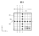
- FIG. 3 is a layout diagram illustrating a part (1/4) of the coordinate calibration sample according to the first embodiment. The enlarged view explaining the structure of a unit exposure pattern.
- FIG. 3 is a diagram for explaining a method for manufacturing a coordinate calibration sample according to the first embodiment. The figure explaining the positional relationship (regularity) of the built-in defect and the center point of the sample for coordinate calibration. The figure explaining the example of a suitable shape used for a built-in defect. The figure explaining a surface inspection apparatus. The flowchart explaining the calibration procedure of the coordinate in a surface inspection apparatus.
- FIG. 2 shows a part of a coordinate calibration sample 200 according to this embodiment.
- FIG. 2 shows only the third quadrant of the coordinate calibration sample 200 in which a defect is formed in a substantially disk-shaped (same shape as the wafer) substrate.
- the configuration of the coordinate calibration sample 200 corresponding to the other quadrants is the same as that of the third quadrant. That is, each quadrant portion is provided with a configuration obtained by rotating the configuration shown in FIG. 2 by 90 °, 180 °, and 270 °, respectively, with the center point (0, 0) of the coordinate calibration sample 200 as the rotation center. .
- the coordinate calibration sample 200 may be referred to as a calibration wafer or a standard sample.
- the material of the substrate constituting the coordinate calibration sample 200 is, for example, silicon, sapphire, silica, or the like.
- an arbitrary unit exposure region 201 is defined on the surface of the coordinate calibration sample 200.
- the unit exposure area 201 may substantially match the size of a chip (virtual chip).
- the unit exposure area 201 is, for example, a quadrangle, and more specifically a square.
- the minimum unit of the exposure area is referred to as “unit exposure area”, but the unit exposure area does not match the size of the area exposed in one exposure process. Sometimes. For example, a plurality of unit exposure areas may be exposed in one exposure process.
- a plurality of unit exposure regions 201 are arranged on the surface of the substrate so as to form a lattice pattern over the entire substrate.
- the unit exposure area 201 is disposed substantially parallel to the x-axis and the y-axis, which are the orthogonal coordinate system (first orthogonal coordinate system) of the substrate.
- the coordinates of the unit exposure area 201 can be expressed by values of “0” to “ ⁇ 7” in the respective axis directions of the orthogonal coordinate system (first orthogonal coordinate system).
- this orthogonal coordinate system (first orthogonal coordinate system) is the same as the coordinate calibration sample described in FIG.
- the center of the coordinate calibration sample 200 substantially coincides with the center of the virtual chip corresponding to (0, 0) that gives the coordinate origin.
- the unit exposure area 201 has the same size as the area exposed in one exposure process.
- the pattern exposed to the unit exposure region 201 is referred to as “unit exposure pattern”.
- a plurality of defect patterns 301 (FIG. 3) corresponding to built-in defects described later are assigned to the unit exposure pattern.
- the defect pattern 301 is an independent pattern like the built-in defect.
- virtual lines connecting a plurality of defect patterns are represented by lines 202 and 203.
- a line 202 (horizontal line) and a line 203 (vertical line) pass through the center point of each unit exposure region 201 and are straight lines parallel to the x-axis and y-axis of the orthogonal coordinate system (first orthogonal coordinate system) of the substrate.
- a line 202 (horizontal line) and a line 203 (vertical line) divide the unit exposure region 201 into four equal parts. This means that a plurality of defect patterns constituting the line 202 (horizontal line) and the line 203 (vertical line) are arranged so as to divide the unit exposure area 201 into four equal parts.
- virtual oblique lines L1 to L13 inclined by a predetermined angle with respect to the x-axis and the y-axis passing through the coordinate origin (0, 0) are respectively formed on the substrate surface.
- the coordinate origin (0, 0) coincides with the intersection position of the virtual line L0 and the virtual line L14.
- the oblique lines L1 to L13 correspond to imaginary lines passing through built-in defects arranged at equal intervals in the radial direction from the coordinate origin (0, 0).
- the oblique line L7 is substantially 45 degrees with respect to the x-axis and the y-axis.
- the maximum value of the number of unit exposure areas 201 arranged in the radial direction from the coordinate origin (0, 0) is N (a natural number of 2 or more, and does not include the unit exposure areas 201 that give the coordinate origin. ).
- N ⁇ 1 diagonal lines can be defined on both sides of the diagonal line L7. Note that the maximum value of the number is obtained in the directions of the virtual line L0 and the virtual line L14.
- FIG. 3 shows an enlarged view of a unit exposure pattern corresponding to the unit exposure region 201.
- FIG. 3 also shows a case where the unit exposure area 201 and the size of the area exposed in one exposure process match.
- the size of the unit exposure area 201 does not necessarily match the area exposed in one exposure process.
- the area exposed in one exposure process may be two unit exposure areas 201. Even in that case, the unit exposure pattern corresponding to one unit exposure region 201 is the same.
- a defect pattern 301 corresponding to a plurality of built-in defects is formed.
- one defect pattern 301 located in the middle of each of the seven defect patterns 301 corresponding to the x-axis direction and the y-axis direction is the center point of the unit exposure region 201 (that is, the center of the unit exposure pattern). Point).
- the distances Lx and Ly between two adjacent built-in defects 301 are substantially equal to 1/7 of one side of the unit exposure region 201. In other words, the distances Lx and Ly are equal to 1 / (M ⁇ 1) of one side of the unit exposure pattern.
- FIG. 4 shows a method for manufacturing the coordinate calibration sample 200 according to this embodiment.
- Step S1 A semiconductor manufacturing apparatus (not shown) applies a resist to the surface of a substantially disk-shaped substrate.
- a known semiconductor manufacturing apparatus is used for applying the resist agent.
- a semiconductor manufacturing apparatus for example, an exposure apparatus repeatedly transfers (exposes) a unit exposure pattern that satisfies a predetermined regularity to the resist surface using an exposure optical system.
- the unit exposure pattern transferred by one exposure is composed of a plurality of defect patterns 301 arranged to cross each other.
- the number of defect patterns 301 giving two lattice lines crossing each other in the unit exposure pattern is M-1 per lattice line (M is a natural number of 2 or more).
- M is a natural number of 2 or more.
- the defect pattern 301 located at the intersection of the two grid lines coincides with the center point of the unit exposure pattern.
- M is the number of unit exposure patterns (or unit exposure regions 201) arranged in the radial direction including the unit exposure pattern used for forming the center point of the lattice pattern finally formed on the substrate surface. Is the maximum value.
- the semiconductor manufacturing apparatus repeats the exposure process so that unit exposure patterns (unit exposure regions 201) are arranged on the entire surface of the substrate to form a lattice pattern. However, as shown in FIG. 2, the arrangement of the unit exposure pattern is determined so that the center point of the substrate and the center point of the unit exposure pattern (that is, the transfer position of the defect pattern 301) coincide.
- Step S3 When the exposure is completed, the semiconductor manufacturing apparatus (for example, an etching apparatus) uses the resist pattern formed using the exposed resist as a mask to etch the substrate surface to form a plurality of built-in defects on the surface of the substrate. To do.
- the semiconductor manufacturing apparatus for example, an etching apparatus
- the coordinates of the built-in defect formed on the surface of the coordinate calibration sample 200 are the coordinate information of the second orthogonal coordinate system defined for the substrate and the local first defined for the unit exposure region 201.
- the position of the unit cell on the substrate is expressed by the coordinate information of the second orthogonal coordinate system
- the position of the built-in defect in the unit cell is expressed by the coordinate information of the first orthogonal coordinate system.
- “0”, “a”, “b”,... Representing the coordinate position in the x direction within one unit exposure area 201 is used.
- a square unit cell is formed by a built-in defect indicated by a black circle in FIG. 5, and a lattice pattern is formed by a set of these unit cells.
- One unit cell is formed by four unit exposure patterns. As shown in FIG. 5, one of the built-in defects located at the intersection of two grid lines and giving the apex of the unit cell coincides with the center point of the coordinate calibration sample 200 (substrate). (Rule 1).
- the unit cells are formed at equal intervals along one side of the unit cell.
- the number of embedded defects is given by N + 1 including two built-in defects that give the vertex of the unit cell (Rule 2).
- FIG. 5 shows an example in which N is seven (see FIG. 2). For this reason, on each side constituting the unit cell, two built-in defects that give the vertexes are included, and eight built-in defects are arranged at equal intervals. Focusing on the oblique line L1, from FIG. 5, the distance from the center point 204 to the built-in defect 303 at the coordinate (a, 1) and the coordinate (b, 2) from the built-in defect 303 at the coordinate (a, 1). It can be seen that the distance to the built-in defect 304 is substantially equal.
- This distance is the distance between the built-in defect 304 at the coordinate (b, 2) and the built-in defect at the coordinate (c, 3), and the built-in defect at the coordinate (c, 3) and the coordinate (d, 4).
- the distance to a certain built-in defect is the same. This means that the distance between two built-in defects adjacent to each other on the oblique line L1 is equal.
- the distance from the center 204 to the built-in defect 305 at the coordinate (b, 1) and the distance from the built-in defect 305 at the coordinate (b, 1) to the built-in defect 306 at the coordinate (d, 2) are substantially It can be seen that they are equal.
- This distance is the same for the distance between the built-in defect 306 at the coordinate (d, 2) and the built-in defect at the coordinate (f, 3). That is, it means that the distance between two built-in defects adjacent to each other on the oblique line L2 is equal.
- the distances between two built-in defects adjacent on each oblique line are all equal. That is, when the maximum value of the number of unit cells arranged in the radial direction from the center of the coordinate calibration sample 200 (substrate) is N (natural number of 2 or more), the unit cells are formed at equal intervals along one side of the unit cell.
- N natural number of 2 or more
- the distance between two built-in defects adjacent on the same diagonal line is always equal. For this reason, in the calibration sample 200 of the present embodiment, imperfections appear at substantially uniform intervals in each radial direction and circumferential direction.
- this coordinate calibration sample 200 In the case of this coordinate calibration sample 200, the distance between two built-in defects appearing in the same radial direction depends on the azimuth angle with respect to the coordinate origin (0, 0) (although it depends on the direction of the oblique line), The appearance frequency of built-in defects is uniform in any azimuth direction. For this reason, when the coordinate calibration sample 200 is used for calibration of the coordinate system (second orthogonal coordinate system) of the surface inspection apparatus that manages the coordinates in the polar coordinate system (R- ⁇ method), compared to the conventional calibration sample. Thus, a large amount of positional deviation information (error information) in the radial direction can be acquired. For this reason, the accuracy of the coordinate correction information is also greatly improved. As a result, the coordinate accuracy of the surface inspection apparatus can be significantly improved as compared with the conventional example.
- the coordinate calibration sample 200 can be manufactured by various methods.
- the coordinate calibration sample 200 can be manufactured by a so-called semiconductor process (consisting of exposure and etching).
- the coordinate calibration sample 200 can be manufactured by FIB (Focused Ion Beam).
- FIB Fluorine-Beam
- FIB has limitations on the shape and size that can be processed, and there is a difficulty in processing uniformity.
- the shape which can be processed is limited to a concave shape.
- the coordinate calibration sample 200 is manufactured by using a semiconductor process, it is desirable to determine the interval between the manufacturing defects according to the specifications of the exposure original plate.
- the coordinate calibration sample 200 is manufactured by a semiconductor process, the degree of freedom in changing the gap between built-in defects can be greatly increased according to the calibration target accuracy.
- At least one of the shape and size of the built-in defect may be determined by the configuration of the surface inspection apparatus (at least one of the spatial arrangement of detectors and the opening size).
- the specification of the built-in defect is selected according to the configuration of the surface inspection apparatus. For example, the specifications are determined so that a plurality of built-in defects are not included in the same detection field of view of the surface inspection apparatus and in an area corresponding to the resolution of the processing apparatus.
- ⁇ Built-in defects may be designed in consideration of the incident angle of the inspection illumination of the surface inspection device. For example, when a rectangular or fine line defect is detected, the optical diffraction angle of the built-in defect is taken into consideration.
- the coordinate calibration sample 200 includes a material (for example, at least one of SiO 2 and SiN) that is stable with respect to the usage environment of the surface inspection apparatus. It is desirable that the coordinate calibration sample 200 includes a material that is substantially stable or substantially resistant to light of a predetermined wavelength.
- a predetermined wavelength for example, an ultraviolet (UV) region, a far infrared (DUV: deep UV), or an extreme ultraviolet (EUV) is considered. More specifically, a band of approximately 10 nm to 400 nm can be considered.
- the built-in defect is a material capable of obtaining a sufficient scattered light intensity with respect to the illumination condition of the surface inspection apparatus.
- the reflection coefficient and absorption coefficient with respect to the illumination wavelength are taken into consideration.
- the imperfection has a shape capable of obtaining stable scattered light with respect to the illumination conditions of the surface inspection apparatus. For example, it is desirable that the shape does not interfere with the illumination wavelength or does not hinder calibration.
- the built-in defect preferably has a shape that provides stable scattered light with respect to the illumination conditions of the surface inspection apparatus. However, consideration should be given so that the lighting energy is not stabilized or damaged.
- the built-in defect preferably has the same scattered light intensity regardless of the azimuth even if the illumination wavelength of the surface inspection apparatus changes. For example, it is preferable that the Rayleigh scattering phenomenon occurs at about 1/3 or less of the illumination wavelength.
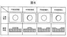
- FIG. 6 shows an example of a shape suitable for use in a built-in defect.
- FIG. 6 shows columnar protrusions, hemispherical protrusions, cylindrical depressions, and hemispherical depressions as examples of shapes suitable for use in a built-in defect.
- the shape and size of the built-in defect is smaller than the illumination wavelength of the surface inspection apparatus, more specifically, sufficiently small, and preferably substantially the same from any direction. Therefore, the shape of the built-in defect is preferably a cylinder and a hemisphere when viewed from above, and it is easy to manufacture as an exposure process and satisfies the above-described requirements.
- the shape of the built-in defect can be selected with a very high degree of freedom depending on the combination of the exposure master specifications and the exposure process.
- a planar shape such as a quadrangle (an aspect ratio can also be selected) and a circle (a sphere) can be selected, and a size (area, height, volume) can also be selected.
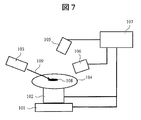
- FIG. 7 shows a surface inspection apparatus that calibrates coordinates using the above-described coordinate calibration sample 200.
- the spindle 102 is a mechanism that rotates the placed coordinate calibration sample 200 at the time of coordinate calibration and rotates the placed wafer 104 at the time of inspection.
- the wafer 104 will be described.
- the XY stage 101 is a mechanism that linearly moves the spindle 102 in the radial direction of the wafer 104 while the wafer 104 is rotating.
- the illumination optical system 103 includes a light source and an optical element.
- the optical element includes a mirror and a lens.
- the illumination optical system 103 irradiates the wafer 104 with light and forms an illumination area 108 on the substrate surface.
- the locus of the illumination area 108 is substantially spiral or concentric.
- the combination of the spindle 102 and the stage 101 realizes the R- ⁇ method.
- the first detection optical system 105 includes a lens for collecting the light scattered from the wafer 104 and a detector for converting the scattered light into first data.
- the first detection optical system 105 may be configured by an imaging system including an imaging lens, a spatial filter, and an image sensor having a plurality of pixels.
- the second detection optical system 106 includes a lens that collects light scattered from the wafer 104 and a detector that converts the scattered light into second data.
- the second detection optical system 106 may be configured by an imaging system including an imaging lens, a spatial filter, and an image sensor having a plurality of pixels.
- the first detection optical system 105 and the second detection optical system 106 are disposed at spatially different positions.
- the first data and the second data are transmitted to the processing system 107 and processed.
- the processing system 107 detects defects on the wafer 104 using at least one of the first data and the second data. Defect detection is performed by comparing at least one of the first data, the second data, and data obtained by performing predetermined processing on the first and second data with a threshold value. For example, when there is data larger than the threshold, the processing system 107 determines that the data is information from a defect.
- the processing system 107 stores the coordinates from which data determined to be defective is obtained in a memory (not shown).
- the processing system 107 includes a display for presenting the inspection result to the operator.
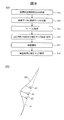
- FIG. 8 shows the flow of calibration processing executed by the processing system 107.
- Step S11 Prior to the inspection of the wafer 104, the surface inspection apparatus uses the coordinate calibration sample 200 as an inspection target.
- Step S12 The processing system 107 compares the inspection data of the built-in defect detected for the coordinate calibration sample 200 with the data related to the coordinate calibration sample 200 stored in advance. More specifically, the processing system 107 compares the approximate curve 801 for the built-in defect detected as described in FIG. 8B with an arbitrary oblique line (for example, L1) stored in advance. . The processing system 107 obtains the positional deviation ⁇ from the result of this comparison. This misalignment corresponds to the error information described above.
- Step S13 The processing system 107 calculates an error correction amount ( ⁇ ) that cancels the positional deviation ⁇ . Since the positional deviation ⁇ may vary depending on the coordinate position, the processing system 107 may obtain a plurality of error correction amounts ( ⁇ ) (for example, ⁇ 1, ⁇ 2, and ⁇ 3) (see FIG. 8 (b)).
- ⁇ error correction amount
- Step S14 The processing system 107 creates a correction map by associating the obtained error correction amount ( ⁇ ) with the coordinates, and stores the created correction map in the memory.
- the coordinate error calibration process (coordinate calibration process) inherent to the driving mechanism of the surface inspection apparatus is thus completed.
- Step S15 Thereafter, inspection of the wafer 104 is started.
- the wafer 104 is an arbitrary inspection sample.
- Step S16 The processing system 107 drives and controls the spindle 102 and the stage 101 so that the inspection region is positioned at the coordinate position corrected using the correction map created earlier.
- the coordinate calibration sample 200 may be incorporated in the surface inspection apparatus. In that case, the coordinate calibration sample 200 substantially becomes one element of the surface inspection apparatus.
- the present invention is not limited to the above-described embodiments, and includes various modifications.
- the above-described embodiments have been described in detail for easy understanding of the present invention, and it is not necessary to provide all the configurations described.
- a part of one embodiment can be replaced with the configuration of another embodiment.
- the structure of another Example can also be added to the structure of a certain Example.
- a part of the configuration of another embodiment can be added, deleted, or replaced.
- each of the above-described configurations, functions, processing units, processing means, and the like may be realized by hardware by designing a part or all of them with, for example, an integrated circuit.
- Each of the above-described configurations, functions, and the like may be realized by the processor interpreting and executing a program that realizes each function (that is, in software).
- Information such as programs, tables, and files that realize each function can be stored in a storage device such as a memory, a hard disk, or an SSD (Solid State Drive), or a storage medium such as an IC card, an SD card, or a DVD.
- Control lines and information lines indicate what is considered necessary for the description, and do not represent all control lines and information lines necessary for the product. In practice, it can be considered that almost all components are connected to each other.
Landscapes
- Physics & Mathematics (AREA)
- General Physics & Mathematics (AREA)
- Health & Medical Sciences (AREA)
- Life Sciences & Earth Sciences (AREA)
- Chemical & Material Sciences (AREA)
- Analytical Chemistry (AREA)
- Biochemistry (AREA)
- General Health & Medical Sciences (AREA)
- Immunology (AREA)
- Pathology (AREA)
- Investigating Materials By The Use Of Optical Means Adapted For Particular Applications (AREA)
- Testing Or Measuring Of Semiconductors Or The Like (AREA)
Abstract
(1)円板状の基板と、(2)正方形を単位格子とする格子パターンを前記基板の表面に形成する複数個の作り込み欠陥であり、前記格子パターンの中心点を与える作り込み欠陥が前記基板の中心点と一致し、前記基板の中心点から半径方向に並ぶ前記単位格子の個数の最大値をN(2以上の自然数)個とするとき、前記単位格子の一辺に沿って等間隔に形成される前記作り込み欠陥の個数を、前記単位格子の頂点を与える2つの作り込み欠陥を含んでN+1個とする、複数個の作り込み欠陥とを有する座標校正用試料を提案する。
Description
本発明は、試料上の欠陥を検査する表面検査装置で使用する座標校正用試料及びその作製方法に関する。
半導体製造工程では、半導体基板(ウェーハ)表面の異物、傷等の欠陥は、ウェーハ上に形成される配線の絶縁不良や短絡等の不良原因になり、キャパシタの絶縁不良やゲート酸化膜などの破壊の原因にもなる。よって、半導体製造工程においてウェーハ表面の欠陥を検出し、半導体製造工程へフィードバックすることは重要である。
このような欠陥の検出には、いわゆる表面検査装置が使用される。表面検査装置の一例には、検査光を基板へ照射し、その散乱光を検出することにより、基板上の欠陥を検出する光学式検査装置がある。光学式検査装置は、鏡面ウェーハ(ベアウェーハ)を検査する表面検査装置と、回路パターンが形成された後のウェーハを検査するパターン付きウェーハ表面検査装置とに大別することができる。本明細書では、いずれの検査装置も「表面検査装置」といい、その検査を「表面検査」という。
半導体デバイスの製造工程では、ウェーハ表面に塗布したレジストにパターンを転写してレジストパターンを作成する工程と、作成されたレジストパターンをマスクとしてエッチングする工程と、ウェーハ表面の不要な部分を除去する工程が実行される。このため、ウェーハ表面に付着した異物や欠陥等は、歩留まりを低下させる大きな要因となる。
そこで、各製造工程では、前述の表面検査装置を使用し、ウェーハ表面に付着している異物やウェーハ表面に存在する欠陥などを高感度、かつ、高スループットで検出して管理している。また、表面検査において、ウェーハ表面の粗さは、フォトリソグラフィー工程の性能を左右するだけでなく、検出感度にも大きく影響する。このため、ウェーハ表面の粗さの計測も必要性が高い。
ところで、製造プロセスの歩留まりの改善および維持には、欠陥の発生原因の特定が必要であり、高倍率での観察が必要である。この観察には、表面観察装置が使用され得る。表面観察装置は、表面検査装置から欠陥の位置を受け取った後、荷電粒子線等を使用して、表面検査装置よりも高い倍率でウェーハ表面を観察する。表面観察装置の座標精度は一般に表面検査装置よりも高い。このため、表面観察装置が素早く欠陥を見つけるためには、表面検査装置に比してより高い座標精度が要求される。つまり、表面検査装置の座標精度は、事前に正しく校正されている必要がある。
表面検査装置の欠陥座標精度の校正には、校正点を配列したウェーハ(座標校正用試料)が使用される。図1に、座標校正用試料の従来例を示す。従来用いられている座標校正用試料では、ウェーハの表面に、単位格子(仮想チップ)をx軸の方向とy軸の方向のそれぞれに等間隔に配列する仮想の格子パターンを設定し、前記仮想の格子パターンを構成する単位格子の中心点に凹状の欠陥(疑似欠陥)を作成している。個々の疑似欠陥が、個々の校正点に対応する。図1は、この仮想的な格子パターンのイメージと半径方向に等間隔な関係にある単位格子の位置関係を表している。
極座標系で座標を管理する表面検査装置は、ウェーハを回転させながらステージを半径方向に移動させることにより、検査視野をウェーハ表面上で螺旋状に移動させ、ウェーハの全面を検査する。本明細書では、このようにウェーハの回転と直進移動とを同時に行いながら検査する方式を「R-θ方式」とも呼称する。R-θ方式の場合、検査視野の軌跡は、実質的な螺旋状となるか同心円状となる。このため、R-θ方式を用いる表面検査装置では、R(半径方向の位置)とθ(回転方向の位置)とで与えられる座標の誤差情報をウェーハ全面に亘って検査の開始前に取得しておく必要がある。
しかし、前述したように、格子パターンを構成する単位格子の各中心点にのみ擬似欠陥を作り込む場合、ウェーハの中心点から放射線上に等しい間隔で現れる擬似欠陥を含む単位格子(仮想チップ)の位置は、図1における「A」、「B」、「C」、「D」の位置に限られる。このため、表面検査装置に固有の座標補正情報(誤差情報を補正する情報)をウェーハ内で均一に取得することが出来ない。
すなわち、ウェーハ面内の座標補正情報を与える校正点の分布にムラ(粗密)があるため、従来用いられている座標校正試料(図1)によっては、ウェーハ面内にランダムに存在する座標の誤差情報を隈なく取得することが困難である。このため、従来の表面検査装置では、誤差情報が疎な領域について、周辺領域の誤差情報を内挿補間して誤差情報を生成している。しかし、これでは補正結果にバラツキが生じ、要求精度を満たさないことを発明者は見出した。
上記課題を解決するために、本明細書は、半径及び円周方向のそれぞれについて実質的に均一な間隔で欠陥座標校正用の基準点(校正点)を与えるように作り込み欠陥を配置した座標校正用試料を提案する。代表的な発明の一つである座標校正用試料は、「円板状の基板と、正方形を単位格子とする格子パターンを前記基板の表面に形成する複数個の作り込み欠陥であり、前記格子パターンの中心点を与える作り込み欠陥が前記基板の中心点と一致し、前記基板の中心点から半径方向に並ぶ前記単位格子の個数の最大値をN(2以上の自然数)個とするとき、前記単位格子の一辺に沿って等間隔に形成される前記作り込み欠陥の個数を、前記単位格子の頂点を与える2つの作り込み欠陥を含んでN+1個とする、複数個の作り込み欠陥と」を有している。
また、代表的な発明の一つである座標校正用試料の作製方法は、「円板状の基板の表面にレジストを塗布するステップと、複数回の露光工程により、前記レジストの表面に単位露光パターンを順次転写するステップであり、前記レジストの表面に形成される格子パターンの中心点の形成に使用される前記単位露光パターンを含んで半径方向に並ぶ前記単位露光パターンの個数の最大値をM個(2以上の自然数)とするとき、前記単位露光パターンは、第1の格子線を構成するM-1個の欠陥パターンと、前記第1の格子線と十字に交差する第2の格子線を構成するM-1個の欠陥パターンとを有し、かつ、前記第1及び第2の格子線に共通する欠陥パターンが前記単位露光パターンの中心を与え、かつ、各格子線上で隣接する2つの欠陥パターンの間隔が前記単位露光パターンの1辺の1/(M-1)で与えられるステップと、露光済みの前記レジストを用いて形成されたパターンをマスクとして用いて前記基板の表面をエッチングし、前記基板の表面に複数個の作り込み欠陥を形成するステップと」を有している。
本発明によれば、半径及び円周方向のそれぞれについて実質的に均一な間隔で欠陥座標校正用の基準点(校正点)を与えるように作り込み欠陥を配置した座標校正用試料を実現できる。この結果、表面検査装置の座標精度を従来に比して格段に向上することができる。前述した以外の課題、構成及び効果は、以下の実施の形態の説明により明らかにされる。
以下、図面に基づいて、本発明の実施の形態を説明する。なお、本発明の実施の態様は、後述する形態例に限定されるものではなく、その技術思想の範囲において、種々の変形が可能である。
(実施例1)
図2に、本実施例に係る座標校正用試料200の一部分を示す。図2は、ほぼ円板状(ウェーハと同形状)の基板に作り込み欠陥を形成した座標校正用試料200の第3象限部分のみを表している。なお、他の象限部分に対応する座標校正用試料200の構成は第3象限と同様である。すなわち、各象限部分には、図2に示した構成を、座標校正用試料200の中心点(0,0)を回転中心としてそれぞれ90°、180°、270°回転した構成が設けられている。
図2に、本実施例に係る座標校正用試料200の一部分を示す。図2は、ほぼ円板状(ウェーハと同形状)の基板に作り込み欠陥を形成した座標校正用試料200の第3象限部分のみを表している。なお、他の象限部分に対応する座標校正用試料200の構成は第3象限と同様である。すなわち、各象限部分には、図2に示した構成を、座標校正用試料200の中心点(0,0)を回転中心としてそれぞれ90°、180°、270°回転した構成が設けられている。
本明細書においては、座標校正用試料200を、校正用ウェーハや標準試料と称呼することがある。座標校正用試料200を構成する基板の材質は、例えばシリコン、サファイア、シリカ等である。図2に示すように、本実施例においては、座標校正用試料200の表面上に任意の単位露光領域201を定義する。単位露光領域201は、実質的にチップ(仮想チップ)の大きさと一致する場合がある。単位露光領域201は例えば四角形であり、より具体的には正方形である。なお、本明細書では、規則性の説明の都合上、露光領域の最小単位を「単位露光領域」と呼ぶが、単位露光領域は、1回の露光工程で露光される領域の大きさと一致しないことがある。例えば、1回の露光工程では複数個分の単位露光領域が露光されることがある。
本実施例の場合、基板の表面には、複数個の単位露光領域201が基板全体で格子パターンを形成するように配置する。このため、単位露光領域201は、基板の直交座標系(第1の直交座標系)であるx軸とy軸に対してそれぞれ実質的に平行に配置される。図2の場合、単位露光領域201の座標は、直交座標系(第1の直交座標系)の各軸方向について、「0」~「-7」の値で表現することができる。参考までに、この直交座標系(第1の直交座標系)は、図1で説明した座標校正用試料と同じである。座標校正用試料200の中心は、座標原点を与える(0,0)に対応する仮想チップの中心と実質的に一致する。
以下では、単位露光領域201が1回の露光工程で露光される領域の大きさと同じであるものとする。本明細書では、単位露光領域201に露光するパターンを「単位露光パターン」という。単位露光パターンには、後述する作り込み欠陥に対応する欠陥パターン301(図3)が複数個割り当てられている。欠陥パターン301は、作り込み欠陥と同様、独立したパターンである。図2においては、複数の欠陥パターンを結ぶ仮想線を線202と線203で表現している。線202(横線)及び線203(縦線)は、各単位露光領域201の中心点を通って、基板の直交座標系(第1の直交座標系)のx軸とy軸に平行な直線である。図2に示すように、線202(横線)及び線203(縦線)は、単位露光領域201を4等分する。このことは、線202(横線)及び線203(縦線)を構成する複数個の欠陥パターンが、単位露光領域201を4等分するように配置されることを意味する。
後述する規則性の下、基板表面に作り込み欠陥を形成すると、座標原点(0,0)を通るx軸及びy軸に対してそれぞれ所定の角度だけ傾斜した仮想の斜線L1~L13を基板表面に定義することできる。ここで、座標原点(0,0)は、仮想の線L0と仮想の線L14の交点位置と一致する。斜線L1~L13は、座標原点(0,0)から放射方向に等間隔に配置された作り込み欠陥を通る仮想線にそれぞれ対応する。斜線L1~L13のうち斜線L7は、x軸及びy軸に対して実質的に45度である。
以下では、仮想の斜線L1~L13の設定を可能にする規則性について説明する。ここでは、座標原点(0,0)から半径方向に配列される単位露光領域201の数の最大値をN(2以上の自然数であり、座標原点を与える単位露光領域201を個数に含まない。)とする。この場合、図2に示すように、斜線L7の両側には、それぞれN-1本の斜線を定義することができる。なお、個数の最大値は、仮想の線L0と仮想の線L14の方向について得られる。
図3に、単位露光領域201に対応する単位露光パターンの拡大図を示す。図3も、単位露光領域201と1回の露光工程で露光される領域の大きさが一致する場合について表している。前述したように、単位露光領域201の大きさは1回の露光工程で露光される領域と必ずしも一致する必要はない。例えば1回の露光工程で露光される領域は、単位露光領域201の2個分であっても良い。その場合でも、1つの単位露光領域201に対応する単位露光パターンは同じである。
単位露光パターンには複数の作り込み欠陥に対応する欠陥パターン301が形成される。本実施例における座標校正用試料200では、座標原点(0,0)から半径方向に配列される単位露光領域201の数の最大値Mが座標原点(0,0)に形成に使用される単位露光領域201を含んで8個であるので、欠陥パターン301の数は、x軸の方向とy軸の方向のそれぞれについて7個で与えられる。この個数の関係が重要である。なお、個数の最大値は、図2の場合、仮想の線L0と仮想の線L14の方向について得られる。
ここで、x軸の方向とy軸の方向に対応する各7個の欠陥パターン301のうち真ん中に位置する1個の欠陥パターン301が、単位露光領域201の中心点(すなわち単位露光パターンの中心点)と一致する。また、隣り合う2つの作り込み欠陥301の距離Lx及びLyは、単位露光領域201の1辺の1/7に実質的に等しい。換言すると、距離Lx及びLyは、単位露光パターンの1辺の1/(M-1)に等しい。
図4に、本実施例に係る座標校正用試料200の製造方法を示す。
(ステップS1)
不図示の半導体製造装置は、ほぼ円板状の基板の表面にレジストを塗布する。レジスト剤の塗布には既知の半導体製造装置を使用する。
(ステップS1)
不図示の半導体製造装置は、ほぼ円板状の基板の表面にレジストを塗布する。レジスト剤の塗布には既知の半導体製造装置を使用する。
(ステップS2)
次に、半導体製造装置(例えば露光装置)は、露光光学系を使用して、所定の規則性を満たす単位露光パターンをレジスト表面に繰り返し転写(露光)する。1回の露光で転写される単位露光パターンは、図3に示すように、十字に交差するように配列された複数個の欠陥パターン301で構成される。ここで、単位露光パターン内で十字に交差する2本の格子線を与える欠陥パターン301の個数は、格子線1本につきM-1個(Mは2以上の自然数)である。また、2本の格子線の交点に位置する欠陥パターン301は単位露光パターンの中心点に一致する。
次に、半導体製造装置(例えば露光装置)は、露光光学系を使用して、所定の規則性を満たす単位露光パターンをレジスト表面に繰り返し転写(露光)する。1回の露光で転写される単位露光パターンは、図3に示すように、十字に交差するように配列された複数個の欠陥パターン301で構成される。ここで、単位露光パターン内で十字に交差する2本の格子線を与える欠陥パターン301の個数は、格子線1本につきM-1個(Mは2以上の自然数)である。また、2本の格子線の交点に位置する欠陥パターン301は単位露光パターンの中心点に一致する。
前述したように、Mは、最終的に基板表面に形成される格子パターンの中心点の形成に使用される単位露光パターンを含んで半径方向に並ぶ単位露光パターン(又は単位露光領域201)の個数の最大値である。半導体製造装置は、単位露光パターン(単位露光領域201)が基板の全面に配列されて格子パターンを形成するように露光工程を繰り返す。ただし、図2に示すように、基板の中心点と単位露光パターンの中心点(すなわち、欠陥パターン301の転写位置)が一致するように単位露光パターンの配置を決定する。
(ステップS3)
露光が終了すると、半導体製造装置(例えばエッチング装置)は、露光済みのレジストを用いて形成されたレジストパターンをマスクとして用いて基板表面をエッチングし、基板の表面に複数個の作り込み欠陥を形成する。
露光が終了すると、半導体製造装置(例えばエッチング装置)は、露光済みのレジストを用いて形成されたレジストパターンをマスクとして用いて基板表面をエッチングし、基板の表面に複数個の作り込み欠陥を形成する。
以上で、座標原点(0,0)から放射方向に等間隔に作り込み欠陥が現れる座標校正用試料200を製造するために使用する単位露光領域201に求められる規則性の説明を終了する。続いて、座標校正用試料200の表面に形成された作り込み欠陥に求められる規則性について説明する。
以下では、座標校正用試料200の表面に形成された作り込み欠陥の座標を、基板について定義された第2の直交座標系の座標情報と、単位露光領域201について定義された局所的な第1の直交座標系の座標情報と組み合わせて説明する。例えば基板上における単位格子の位置は第2の直交座標系の座標情報により、単位格子内の作り込み欠陥の位置は第1の直交座標系の座標情報により表現する。図3の例であれば、1つの単位露光領域201内のx方向の座標位置を表す「0」、「a」、「b」、…を使用する。y軸方向についても同様である。第1及び第2の直交座標系を用いれば、個々の作り込み欠陥の位置を特定することができる。
図5を用いて、作り込み欠陥と座標校正用試料200の中心204との間に求められる規則性(位置関係)を説明する。座標校正用試料200の表面には、図5において黒丸で示す作り込み欠陥によって正方形の単位格子が形成されており、これら単位格子の集合により格子パターンが形成される。なお、1つの単位格子は、4つの単位露光パターンによって形成される。図5に示すように、2本の格子線の交点に位置する作り込み欠陥であって、単位格子の頂点を与える作り込み欠陥の1つが、座標校正用試料200(基板)の中心点と一致する(規則1)。ここで、座標校正用試料200の中心点から半径方向に並ぶ単位格子の個数の最大値をN(2以上の自然数)個とするとき、単位格子の一辺に沿って等間隔に形成される作り込み欠陥の個数は、単位格子の頂点を与える2つの作り込み欠陥を含んでN+1個で与えられる(規則2)。
図5は、Nが7個(図2参照)の例である。このため、単位格子を構成する各辺上には、その頂点を与える2つの作り込み欠陥を含み、8個の作り込み欠陥が等間隔に配列されている。斜線L1に着目すると、図5より、中心点204から座標(a,1)にある作り込み欠陥303までの距離と、座標(a,1)にある作り込み欠陥303から座標(b,2)にある作り込み欠陥304までの距離は実質的に等しいことが分かる。この距離は、座標(b,2)の作り込み欠陥304と座標(c,3)にある作り込み欠陥との距離、座標(c,3)にある作り込み欠陥と座標(d,4)にある作り込み欠陥との距離、…とも等しくなる。このことは、斜線L1上で隣り合う2つの作り込み欠陥の距離は、いずれも等しいことを意味する。
次に、斜線L2に着目する。中心204から座標(b,1)にある作り込み欠陥305までの距離と、座標(b,1)にある作り込み欠陥305と座標(d,2)にある作り込み欠陥306までの距離は実質的に等しいことが分かる。この距離は、座標(d,2)にある作り込み欠陥306と座標(f,3)にある作り込み欠陥との距離その他についても等しい。つまり、斜線L2上で隣り合う2つの作り込み欠陥の距離は、いずれも等しいことを意味する。
他の斜線L3、L4…L13についても、各斜線上で隣接する2つの作り込み欠陥の距離はいずれも等しい値になる。つまり、座標校正用試料200(基板)の中心から半径方向に並ぶ単位格子の個数の最大値をN(2以上の自然数)個とするとき、単位格子の一辺に沿って等間隔に形成される作り込み欠陥の個数を、単位格子の頂点を与える2つの作り込み欠陥を含んでN+1個に定めることにより、同じ斜線上で隣り合う2つの作り込み欠陥の距離は常に等しい関係になる。このため、本実施例の校正用試料200では、各半径方向及び円周方向のそれぞれについて実質的に均一な間隔で作り込み欠陥が出現する。
なお、この座標校正用試料200の場合、同一半径方向上に出現する2つの作り込み欠陥の距離は座標原点(0,0)に対する方位角に依存するが(斜線の向きに依存するが)、いずれの方位角方向についても作り込み欠陥の出現頻度は均等になる。このため、極座標系(R-θ方式)で座標を管理する表面検査装置の座標系(第2の直交座標系)の校正に座標校正用試料200を用いる場合、従来の校正用試料に比して半径方向における位置ずれ情報(誤差情報)を多く取得することができる。このため、座標補正情報の精度も格段に向上する。結果的に、表面検査装置の座標精度を従来例に比して格段に向上できる。
(実施例2)
本実施例では、座標校正用試料200の作製方法について説明を補足する。座標校正用試料200は、様々な方法で作製することができる。例えば前述したように、いわゆる半導体プロセス(露光とエッチングで構成される)によって座標校正用試料200を作製することができる。また、FIB(Focused Ion Beam)によっても座標校正用試料200を作製することができる。もっとも、座標校正用試料200の作製には、半導体プロセスを採用する方が望ましい。
本実施例では、座標校正用試料200の作製方法について説明を補足する。座標校正用試料200は、様々な方法で作製することができる。例えば前述したように、いわゆる半導体プロセス(露光とエッチングで構成される)によって座標校正用試料200を作製することができる。また、FIB(Focused Ion Beam)によっても座標校正用試料200を作製することができる。もっとも、座標校正用試料200の作製には、半導体プロセスを採用する方が望ましい。
その理由は、FIBで作製した作り込み欠陥の配列精度は、FIB装置の性能に依存するためである。また、FIBには加工可能な形状及びサイズに制限があり、加工均一性にも難点がある。例えばFIBでは、加工可能な形状が凹型に限定される。さらに、FIBでは、個々の作り込み欠陥の加工に要する時間が長く、座標校正用試料200の製造原価が高くなる可能性もある。
一方、半導体プロセスであれば、これらのデメリットがない。なお、半導体プロセスを用いて座標校正用試料200を作製する場合には、露光原版の仕様に応じ、作り込み欠陥の間隔を決定することが望まれる。また、半導体プロセスによって座標校正用試料200を製造する場合、校正目標精度に応じて、作り込み欠陥の間隔の変更自由度を非常に高くできる。
例えば作り込み欠陥の形状及びサイズの少なくとも1つは、表面検査装置の構成(検出器の空間的配置及び開口サイズの少なくとも1つ)により決定すれば良い。本実施例では、表面検査装置の構成に応じて作り込み欠陥の仕様を選択している。例えば表面検査装置の同一検出視野内及び処理装置の分解能に対応する領域内に複数の作り込み欠陥が含まれないように仕様を決定する。
作り込み欠陥は、表面検査装置の検査照明の入射角を考慮して設計される場合もある。例えば長方形又は細線状の欠陥を検出した場合には、作り込み欠陥の光学的回折角度に配慮する。
座標校正用試料200は、表面検査装置の使用環境に対して安定である材料(例えばSiO2及びSiNのうち少なくとも1つ)を含む方が好ましい場合もある。座標校正用試料200は、所定波長の光に対して実質的に安定又は実質的に耐性を有する材料を含む方が望ましい。所定波長としては、例えば紫外線(UV:ultraviolet)領域、遠赤外線(DUV:deep UV)、極紫外線(EUV:extreme UV)が考えられる。より具体的には、概ね10nm以上~400nm以下の帯域が考えられる。
さらに、作り込み欠陥は、表面検査装置の照明条件に対して十分な散乱光強度が得られる材料である方が好ましい。ただし、照明波長に対しての反射係数や吸収係数を考慮する。また、作り込み欠陥は、表面検査装置の照明条件に対して安定した散乱光が得られる形状である方が好ましい。例えば照明波長に対して干渉が発生しない、又は、校正に支障を来たさない形状であることが望ましい。
作り込み欠陥は、表面検査装置の照明条件に対して安定した散乱光が得られる形状である方が好ましい。ただし、照明エネルギーに対して安定又はダメージを受けないように考慮する。作り込み欠陥は、表面検査装置の照明波長が変化しても方位角によらず同様の散乱光強度が得られる方が好ましい。例えば概ね照明波長の1/3以下でレーリー散乱現象となる方が好ましい。
(実施例3)
図6に、作り込み欠陥に用いて好適な形状の例を示す。図6には、作り込み欠陥に用いて好適な形状例として、円柱状突起、半球状突起、円柱状窪み、及び半球状窪みを示している。なお、作り込み欠陥の形状及び寸法は、表面検査装置の照明波長に対し小さく、より具体的には十分小さく、どの方向からも実質的に同一が望ましい。よって、作り込み欠陥の形状は、鉛直上方から見て円柱及び半球であることが好ましく、露光プロセスとしても製造が容易であり、前述の要求条件を満たす。
図6に、作り込み欠陥に用いて好適な形状の例を示す。図6には、作り込み欠陥に用いて好適な形状例として、円柱状突起、半球状突起、円柱状窪み、及び半球状窪みを示している。なお、作り込み欠陥の形状及び寸法は、表面検査装置の照明波長に対し小さく、より具体的には十分小さく、どの方向からも実質的に同一が望ましい。よって、作り込み欠陥の形状は、鉛直上方から見て円柱及び半球であることが好ましく、露光プロセスとしても製造が容易であり、前述の要求条件を満たす。
また、作り込み欠陥の形状は、露光原版の仕様と露光プロセスの組合せにより非常に高い自由度で選択することができる。例えば四角形(縦横比も選択可能)、円(球)などの平面的な形状が選択できるし、サイズ(面積、高さ、体積)の選択も可能である。
(実施例4)
図7に、前述した座標校正用試料200を使用して座標を校正する表面検査装置を示す。スピンドル102は、座標校正時には載置された座標校正用試料200を回転させる一方、検査時には載置されたウェーハ104を回転させる機構である。以下では、ウェーハ104について説明する。XYステージ101は、ウェーハ104が回転している間、スピンドル102をウェーハ104の半径方向に直線的に移動させる機構である。
図7に、前述した座標校正用試料200を使用して座標を校正する表面検査装置を示す。スピンドル102は、座標校正時には載置された座標校正用試料200を回転させる一方、検査時には載置されたウェーハ104を回転させる機構である。以下では、ウェーハ104について説明する。XYステージ101は、ウェーハ104が回転している間、スピンドル102をウェーハ104の半径方向に直線的に移動させる機構である。
照明光学系103は、光源及び光学素子を含む。光学素子には、ミラー及びレンズが含まれる。照明光学系103は、ウェーハ104に光を照射し、基板表面上に照明領域108を形成する。照明領域108の軌跡は実質的に螺旋状又は同心円状となる。スピンドル102とステージ101との組み合わせによりR-θ方式が実現される。
第1の検出光学系105は、ウェーハ104から散乱した光を集光するためのレンズと、散乱光を第1のデータに変換する検出器を含む。第1の検出光学系105は、結像レンズと、空間フィルタと、複数の画素を有するイメージセンサを含む結像系で構成される場合もある。第2の検出光学系106は、ウェーハ104から散乱した光を集光するレンズと、散乱光を第2のデータに変換する検出器を含む。第2の検出光学系106は、結像レンズと、空間フィルタと、複数の画素を有するイメージセンサを含む結像系で構成される場合もある。第1の検出光学系105と第2の検出光学系106は空間的に異なる位置に配置される。
第1のデータと第2のデータは処理系107に送信され、処理される。処理系107は、第1のデータ及び第2のデータの少なくとも1つを使用してウェーハ104上の欠陥を検出する。欠陥の検出は、第1のデータ、第2のデータ、並びに、第1及び第2のデータに対して所定の処理を施したデータのうちの少なくとも1つと閾値との比較によって行う。例えば閾値よりも大きいデータがあるとき、処理系107は、当該データは欠陥からの情報であると判定する。処理系107は、欠陥と判定したデータが得られた座標を、不図示のメモリに保存する。処理系107は、検査結果をオペレータに提示するためのディスプレイを含んでいる。
図8に、処理系107によって実行される校正処理の流れを示す。
(ステップS11)
ウェーハ104の検査に先立ち、表面検査装置は、座標校正用試料200を検査対象とする。
(ステップS11)
ウェーハ104の検査に先立ち、表面検査装置は、座標校正用試料200を検査対象とする。
(ステップS12)
処理系107は、座標校正用試料200について検出された作り込み欠陥の検査データと事前に保存されている座標校正用試料200に関するデータとを比較する。より具体的には、処理系107は、図8(b)に記載したように検出した作り込み欠陥に対する近似曲線801と事前に保存しておいた任意の斜線(例えば、L1)とを比較する。処理系107は、この比較の結果から位置ずれΔを得る。この位置ずれが、前述の誤差情報に当たる。
処理系107は、座標校正用試料200について検出された作り込み欠陥の検査データと事前に保存されている座標校正用試料200に関するデータとを比較する。より具体的には、処理系107は、図8(b)に記載したように検出した作り込み欠陥に対する近似曲線801と事前に保存しておいた任意の斜線(例えば、L1)とを比較する。処理系107は、この比較の結果から位置ずれΔを得る。この位置ずれが、前述の誤差情報に当たる。
(ステップS13)
処理系107は、位置ずれΔを相殺する誤差補正量(-Δ)を計算する。位置ずれΔは、座標位置に依存してばらつく可能性があるので、処理系107は、誤差補正量(-Δ)を複数(例えば、-Δ1、-Δ2、-Δ3)得る場合もある(図8(b)参照)。
処理系107は、位置ずれΔを相殺する誤差補正量(-Δ)を計算する。位置ずれΔは、座標位置に依存してばらつく可能性があるので、処理系107は、誤差補正量(-Δ)を複数(例えば、-Δ1、-Δ2、-Δ3)得る場合もある(図8(b)参照)。
(ステップS14)
処理系107は、得られた誤差補正量(-Δ)を座標と対応付けて補正マップを作成し、作成された補正マップをメモリに保存する。以上で、表面検査装置の駆動機構に固有の座標誤差の校正処理(座標校正処理)が終了する。
処理系107は、得られた誤差補正量(-Δ)を座標と対応付けて補正マップを作成し、作成された補正マップをメモリに保存する。以上で、表面検査装置の駆動機構に固有の座標誤差の校正処理(座標校正処理)が終了する。
(ステップS15)
この後、ウェーハ104の検査が開始される。ウェーハ104は、任意の検査試料である。
(ステップS16)
処理系107は、先に作成された補正マップを使用して補正した座標位置に検査領域が位置するようにスピンドル102及びステージ101を駆動制御する。
この後、ウェーハ104の検査が開始される。ウェーハ104は、任意の検査試料である。
(ステップS16)
処理系107は、先に作成された補正マップを使用して補正した座標位置に検査領域が位置するようにスピンドル102及びステージ101を駆動制御する。
なお、座標校正用試料200は表面検査装置の内部に組み込んでも良い。その場合、座標校正用試料200は実質的に表面検査装置の1要素となる。
(他の実施例)
本発明は、上述した実施例に限定されるものでなく、様々な変形例を含んでいる。例えば、上述した実施例は、本発明を分かりやすく説明するために詳細に説明したものであり、必ずしも説明した全ての構成を備える必要はない。また、ある実施例の一部を他の実施例の構成に置き換えることができる。また、ある実施例の構成に他の実施例の構成を加えることもできる。また、各実施例の構成の一部について、他の実施例の構成の一部を追加、削除又は置換することもできる。
本発明は、上述した実施例に限定されるものでなく、様々な変形例を含んでいる。例えば、上述した実施例は、本発明を分かりやすく説明するために詳細に説明したものであり、必ずしも説明した全ての構成を備える必要はない。また、ある実施例の一部を他の実施例の構成に置き換えることができる。また、ある実施例の構成に他の実施例の構成を加えることもできる。また、各実施例の構成の一部について、他の実施例の構成の一部を追加、削除又は置換することもできる。
また、上述した各構成、機能、処理部、処理手段等は、それらの一部又は全部を、例えば集積回路で設計する等によりハードウェアで実現しても良い。また、上記の各構成、機能等は、プロセッサがそれぞれの機能を実現するプログラムを解釈し、実行することにより(すなわちソフトウェア的に)実現しても良い。各機能を実現するプログラム、テーブル、ファイル等の情報は、メモリ、ハードディスク、SSD(Solid State Drive)等の記憶装置、又は、ICカード、SDカード、DVD等の記憶媒体に格納することができる。また、制御線や情報線は、説明上必要と考えられるものを示すものであり、製品上必要な全ての制御線や情報線を表すものでない。実際にはほとんど全ての構成が相互に接続されていると考えて良い。
101…XYステージ
102…スピンドル
103…照明光学系
104…ウェーハ
105…第1の検出光学系
106…第2の検出光学系
107…処理系
108…照明領域
200…座標校正用試料
201…単位露光領域
204…中心点
301…欠陥パターン
303、304、305、306…作り込み欠陥
102…スピンドル
103…照明光学系
104…ウェーハ
105…第1の検出光学系
106…第2の検出光学系
107…処理系
108…照明領域
200…座標校正用試料
201…単位露光領域
204…中心点
301…欠陥パターン
303、304、305、306…作り込み欠陥
Claims (11)
- 円板状の基板であって、
正方形を単位格子とする格子パターンを前記基板の表面に形成する複数個の作り込み欠陥であり、前記格子パターンの中心点を与える作り込み欠陥が前記基板の中心点と一致し、前記基板の中心点から半径方向に並ぶ前記単位格子の個数の最大値をN(2以上の自然数)個とするとき、前記単位格子の一辺に沿って等間隔に形成される前記作り込み欠陥の個数を、前記単位格子の頂点を与える2つの前記作り込み欠陥を含んでN+1個とする、複数個の前記作り込み欠陥
を有する座標校正用試料。 - 請求項1に記載の座標校正用試料において、
前記座標校正用試料は、極座標系で試料の座標を管理する表面検査装置の座標校正に用いられる
ことを特徴とする座標校正用試料。 - 請求項1に記載の座標校正用試料において、
前記作り込み欠陥は、紫外線領域、遠紫外線領域及び/又は極紫外線領域の波長帯の光に対して耐性を有する材料によって構成される
ことを特徴とする座標校正用試料。 - 請求項1に記載の座標校正用試料において、
前記作り込み欠陥は、突起状である
ことを特徴とする座標校正用試料。 - 請求項1に記載の座標校正用試料において、
前記作り込み欠陥は、円柱形状又は半球形状である
ことを特徴とする座標校正用試料。 - 請求項1に記載の座標校正用試料において、
前記作り込み欠陥は、露光及びエッチングで構成される半導体プロセスにより作製される
ことを特徴とする座標校正用試料。 - 円板状の基板の表面にレジストを塗布するステップと、
複数回の露光工程により、前記レジストの表面に単位露光パターンを順次転写するステップであり、前記レジストの表面に形成される格子パターンの中心点の形成に使用される前記単位露光パターンを含んで半径方向に並ぶ前記単位露光パターンの個数の最大値をM個(2以上の自然数)とするとき、前記単位露光パターンは、第1の格子線を構成するM-1個の欠陥パターンと、前記第1の格子線と十字に交差する第2の格子線を構成するM-1個の欠陥パターンとを有し、かつ、前記第1及び第2の格子線に共通する欠陥パターンが前記単位露光パターンの中心を与え、かつ、各格子線上で隣接する2つの欠陥パターンの間隔が前記露光パターンの1辺の1/(M-1)で与えられるステップと、
露光済みの前記レジストを用いて形成されたパターンをマスクとして用いて前記基板の表面をエッチングし、前記基板の表面に複数個の作り込み欠陥を形成するステップと
を有することを特徴とする座標校正用試料の作製方法。 - 請求項7に記載の座標校正用試料の作製方法において、
前記複数個の作り込み欠陥は、正方形を単位格子とする格子パターンを前記基板の表面に形成するものであり、前記格子パターンの中心点を与える作り込み欠陥が前記基板の中心点と一致し、前記基板の中心点から半径方向に並ぶ前記単位格子の個数の最大値をN(自然数)個とするとき、前記単位格子の一辺に沿って等間隔に形成される前記作り込み欠陥の個数を、前記単位格子の頂点を与える2つの作り込み欠陥を含んでN+1個とする
ことを特徴とする座標校正用試料の作製方法。 - 請求項7に記載の座標校正用試料の作製方法において、
前記作り込み欠陥は、紫外線領域、遠紫外線領域又は極紫外線領域の波長帯の光に対して耐性を有する材料によって構成される
ことを特徴とする座標校正用試料の作製方法。 - 請求項7に記載の座標校正用試料の作製方法において、
前記作り込み欠陥は、突起状である
ことを特徴とする座標校正用試料の作製方法。 - 請求項7に記載の座標校正用試料の作製方法において、
前記作り込み欠陥は、円柱形状又は半球形状である
ことを特徴とする座標校正用試料の作製方法。
Priority Applications (3)
| Application Number | Priority Date | Filing Date | Title |
|---|---|---|---|
| US15/528,692 US10444011B2 (en) | 2014-11-25 | 2014-11-25 | Sample for coordinates calibration and method for fabricating the same |
| PCT/JP2014/081015 WO2016084124A1 (ja) | 2014-11-25 | 2014-11-25 | 座標校正用試料及びその作製方法 |
| TW104137526A TW201619597A (zh) | 2014-11-25 | 2015-11-13 | 座標校正用試料及其製作方法 |
Applications Claiming Priority (1)
| Application Number | Priority Date | Filing Date | Title |
|---|---|---|---|
| PCT/JP2014/081015 WO2016084124A1 (ja) | 2014-11-25 | 2014-11-25 | 座標校正用試料及びその作製方法 |
Publications (1)
| Publication Number | Publication Date |
|---|---|
| WO2016084124A1 true WO2016084124A1 (ja) | 2016-06-02 |
Family
ID=56073749
Family Applications (1)
| Application Number | Title | Priority Date | Filing Date |
|---|---|---|---|
| PCT/JP2014/081015 Ceased WO2016084124A1 (ja) | 2014-11-25 | 2014-11-25 | 座標校正用試料及びその作製方法 |
Country Status (3)
| Country | Link |
|---|---|
| US (1) | US10444011B2 (ja) |
| TW (1) | TW201619597A (ja) |
| WO (1) | WO2016084124A1 (ja) |
Families Citing this family (4)
| Publication number | Priority date | Publication date | Assignee | Title |
|---|---|---|---|---|
| CN111176083B (zh) * | 2015-02-23 | 2023-07-28 | 株式会社尼康 | 测量装置、光刻系统、曝光装置、测量方法以及曝光方法 |
| EP4378596A4 (en) * | 2021-07-26 | 2024-11-27 | Konica Minolta, Inc. | REFERENCE SAMPLE FOR COATING DEFECTS AND ITS PRODUCTION METHOD |
| CN116087075A (zh) * | 2022-10-24 | 2023-05-09 | 成都理工大学 | 一种用于碳酸盐岩矿物溶蚀形貌的原位对比研究方法 |
| DE102023102475A1 (de) * | 2023-02-01 | 2024-08-01 | Carl Zeiss Smt Gmbh | Verfahren zur Untersuchung von Proben der Mikrolithographie |
Citations (4)
| Publication number | Priority date | Publication date | Assignee | Title |
|---|---|---|---|---|
| JPH1164239A (ja) * | 1997-08-26 | 1999-03-05 | Nec Corp | 異物検出感度校正用標準サンプル及びその製造方法 |
| JP2000058606A (ja) * | 1998-08-06 | 2000-02-25 | Hitachi Ltd | 検査用標準試料 |
| JP2011075431A (ja) * | 2009-09-30 | 2011-04-14 | Hitachi High-Technologies Corp | 表面欠陥検査装置 |
| JP2012154820A (ja) * | 2011-01-27 | 2012-08-16 | Hitachi High-Technologies Corp | 検査装置 |
Family Cites Families (5)
| Publication number | Priority date | Publication date | Assignee | Title |
|---|---|---|---|---|
| JP3071418B1 (ja) * | 1999-01-28 | 2000-07-31 | 株式会社半導体先端テクノロジーズ | 座標修正装置 |
| US7261983B2 (en) * | 2000-12-08 | 2007-08-28 | Litel Instruments | Reference wafer and process for manufacturing same |
| US7796804B2 (en) * | 2007-07-20 | 2010-09-14 | Kla-Tencor Corp. | Methods for generating a standard reference die for use in a die to standard reference die inspection and methods for inspecting a wafer |
| US8305097B2 (en) * | 2007-09-04 | 2012-11-06 | Texas Instruments Incorporated | Method for calibrating an inspection tool |
| US9826815B2 (en) * | 2010-07-16 | 2017-11-28 | Zen Design Solutions Limited | Application device |
-
2014
- 2014-11-25 US US15/528,692 patent/US10444011B2/en active Active
- 2014-11-25 WO PCT/JP2014/081015 patent/WO2016084124A1/ja not_active Ceased
-
2015
- 2015-11-13 TW TW104137526A patent/TW201619597A/zh unknown
Patent Citations (4)
| Publication number | Priority date | Publication date | Assignee | Title |
|---|---|---|---|---|
| JPH1164239A (ja) * | 1997-08-26 | 1999-03-05 | Nec Corp | 異物検出感度校正用標準サンプル及びその製造方法 |
| JP2000058606A (ja) * | 1998-08-06 | 2000-02-25 | Hitachi Ltd | 検査用標準試料 |
| JP2011075431A (ja) * | 2009-09-30 | 2011-04-14 | Hitachi High-Technologies Corp | 表面欠陥検査装置 |
| JP2012154820A (ja) * | 2011-01-27 | 2012-08-16 | Hitachi High-Technologies Corp | 検査装置 |
Also Published As
| Publication number | Publication date |
|---|---|
| US20170268870A1 (en) | 2017-09-21 |
| TW201619597A (zh) | 2016-06-01 |
| US10444011B2 (en) | 2019-10-15 |
Similar Documents
| Publication | Publication Date | Title |
|---|---|---|
| JP6790172B2 (ja) | 相互レシピ整合性に基づくレシピ選択 | |
| TWI616721B (zh) | 針對極紫外光光罩之臨界尺寸均勻性監測 | |
| TWI649628B (zh) | 用於半導體目標之量測的微分方法及裝置 | |
| CN111340762B (zh) | 用于预测晶片级缺陷可印性的设备及方法 | |
| TWI673487B (zh) | 度量系統、度量設備及度量方法 | |
| JP6412163B2 (ja) | メトロロジーに用いられる基板及びパターニングデバイス、メトロロジー方法、及びデバイス製造方法 | |
| US9390494B2 (en) | Delta die intensity map measurement | |
| TWI627394B (zh) | 用於具有最佳化系統測數之光學測量之設備及方法 | |
| CN109196630B (zh) | 制造以相对装置特征旋转角度定向的计量标靶系统及方法 | |
| US8736849B2 (en) | Method and apparatus for measuring structures on photolithography masks | |
| KR20180097776A (ko) | 개선된 스폿 크기 능력을 갖는 단일 파장 엘립소메트리 | |
| CN110050232A (zh) | 量测设备、光刻系统和测量结构的方法 | |
| WO2016084124A1 (ja) | 座標校正用試料及びその作製方法 | |
| TWI638227B (zh) | 用於檢測一光微影光罩之方法及系統及非暫態電腦可讀媒體 | |
| KR102822950B1 (ko) | 극자외선(Extreme Ultra Violet, 이하 EUV) 마스크 검사 방법, EUV 리소그래피 방법, EUV 리소그래피 제어 장치 및 비 일시적 컴퓨터 판독 가능 매체 | |
| CN114761880A (zh) | 厚光致抗蚀剂层计量目标 | |
| US9965851B2 (en) | Method for inspecting pattern and an apparatus for manufacturing a semiconductor device using the same | |
| JP6414399B2 (ja) | レチクル及びその検査方法 | |
| JP2007180216A (ja) | フレア量の計測方法、フレア量計測用マスク及びデバイスの製造方法 |
Legal Events
| Date | Code | Title | Description |
|---|---|---|---|
| 121 | Ep: the epo has been informed by wipo that ep was designated in this application |
Ref document number: 14907025 Country of ref document: EP Kind code of ref document: A1 |
|
| WWE | Wipo information: entry into national phase |
Ref document number: 15528692 Country of ref document: US |
|
| NENP | Non-entry into the national phase |
Ref country code: DE |
|
| 122 | Ep: pct application non-entry in european phase |
Ref document number: 14907025 Country of ref document: EP Kind code of ref document: A1 |
|
| NENP | Non-entry into the national phase |
Ref country code: JP |