WO2016079985A1 - 有機el素子及び表示装置 - Google Patents
有機el素子及び表示装置 Download PDFInfo
- Publication number
- WO2016079985A1 WO2016079985A1 PCT/JP2015/005748 JP2015005748W WO2016079985A1 WO 2016079985 A1 WO2016079985 A1 WO 2016079985A1 JP 2015005748 W JP2015005748 W JP 2015005748W WO 2016079985 A1 WO2016079985 A1 WO 2016079985A1
- Authority
- WO
- WIPO (PCT)
- Prior art keywords
- organic
- light emitting
- emitting layer
- interlayer
- organic light
- Prior art date
- Legal status (The legal status is an assumption and is not a legal conclusion. Google has not performed a legal analysis and makes no representation as to the accuracy of the status listed.)
- Ceased
Links
Images


Classifications
-
- H—ELECTRICITY
- H10—SEMICONDUCTOR DEVICES; ELECTRIC SOLID-STATE DEVICES NOT OTHERWISE PROVIDED FOR
- H10K—ORGANIC ELECTRIC SOLID-STATE DEVICES
- H10K30/00—Organic devices sensitive to infrared radiation, light, electromagnetic radiation of shorter wavelength or corpuscular radiation
- H10K30/80—Constructional details
- H10K30/865—Intermediate layers comprising a mixture of materials of the adjoining active layers
-
- C—CHEMISTRY; METALLURGY
- C09—DYES; PAINTS; POLISHES; NATURAL RESINS; ADHESIVES; COMPOSITIONS NOT OTHERWISE PROVIDED FOR; APPLICATIONS OF MATERIALS NOT OTHERWISE PROVIDED FOR
- C09K—MATERIALS FOR MISCELLANEOUS APPLICATIONS, NOT PROVIDED FOR ELSEWHERE
- C09K11/00—Luminescent materials, e.g. electroluminescent or chemiluminescent
- C09K11/06—Luminescent materials, e.g. electroluminescent or chemiluminescent containing organic luminescent materials
-
- G—PHYSICS
- G09—EDUCATION; CRYPTOGRAPHY; DISPLAY; ADVERTISING; SEALS
- G09F—DISPLAYING; ADVERTISING; SIGNS; LABELS OR NAME-PLATES; SEALS
- G09F9/00—Indicating arrangements for variable information in which the information is built-up on a support by selection or combination of individual elements
- G09F9/30—Indicating arrangements for variable information in which the information is built-up on a support by selection or combination of individual elements in which the desired character or characters are formed by combining individual elements
-
- H—ELECTRICITY
- H05—ELECTRIC TECHNIQUES NOT OTHERWISE PROVIDED FOR
- H05B—ELECTRIC HEATING; ELECTRIC LIGHT SOURCES NOT OTHERWISE PROVIDED FOR; CIRCUIT ARRANGEMENTS FOR ELECTRIC LIGHT SOURCES, IN GENERAL
- H05B33/00—Electroluminescent light sources
- H05B33/12—Light sources with substantially two-dimensional [2D] radiating surfaces
- H05B33/14—Light sources with substantially two-dimensional [2D] radiating surfaces characterised by the chemical or physical composition or the arrangement of the electroluminescent material, or by the simultaneous addition of the electroluminescent material in or onto the light source
-
- H—ELECTRICITY
- H05—ELECTRIC TECHNIQUES NOT OTHERWISE PROVIDED FOR
- H05B—ELECTRIC HEATING; ELECTRIC LIGHT SOURCES NOT OTHERWISE PROVIDED FOR; CIRCUIT ARRANGEMENTS FOR ELECTRIC LIGHT SOURCES, IN GENERAL
- H05B33/00—Electroluminescent light sources
- H05B33/12—Light sources with substantially two-dimensional [2D] radiating surfaces
- H05B33/14—Light sources with substantially two-dimensional [2D] radiating surfaces characterised by the chemical or physical composition or the arrangement of the electroluminescent material, or by the simultaneous addition of the electroluminescent material in or onto the light source
- H05B33/145—Arrangements of the electroluminescent material
-
- H—ELECTRICITY
- H10—SEMICONDUCTOR DEVICES; ELECTRIC SOLID-STATE DEVICES NOT OTHERWISE PROVIDED FOR
- H10K—ORGANIC ELECTRIC SOLID-STATE DEVICES
- H10K50/00—Organic light-emitting devices
- H10K50/10—OLEDs or polymer light-emitting diodes [PLED]
- H10K50/11—OLEDs or polymer light-emitting diodes [PLED] characterised by the electroluminescent [EL] layers
-
- H—ELECTRICITY
- H10—SEMICONDUCTOR DEVICES; ELECTRIC SOLID-STATE DEVICES NOT OTHERWISE PROVIDED FOR
- H10K—ORGANIC ELECTRIC SOLID-STATE DEVICES
- H10K71/00—Manufacture or treatment specially adapted for the organic devices covered by this subclass
- H10K71/10—Deposition of organic active material
- H10K71/12—Deposition of organic active material using liquid deposition, e.g. spin coating
- H10K71/13—Deposition of organic active material using liquid deposition, e.g. spin coating using printing techniques, e.g. ink-jet printing or screen printing
-
- H—ELECTRICITY
- H10—SEMICONDUCTOR DEVICES; ELECTRIC SOLID-STATE DEVICES NOT OTHERWISE PROVIDED FOR
- H10K—ORGANIC ELECTRIC SOLID-STATE DEVICES
- H10K85/00—Organic materials used in the body or electrodes of devices covered by this subclass
- H10K85/10—Organic polymers or oligomers
- H10K85/111—Organic polymers or oligomers comprising aromatic, heteroaromatic, or aryl chains, e.g. polyaniline, polyphenylene or polyphenylene vinylene
- H10K85/115—Polyfluorene; Derivatives thereof
-
- H—ELECTRICITY
- H10—SEMICONDUCTOR DEVICES; ELECTRIC SOLID-STATE DEVICES NOT OTHERWISE PROVIDED FOR
- H10K—ORGANIC ELECTRIC SOLID-STATE DEVICES
- H10K85/00—Organic materials used in the body or electrodes of devices covered by this subclass
- H10K85/10—Organic polymers or oligomers
- H10K85/151—Copolymers
-
- H—ELECTRICITY
- H10—SEMICONDUCTOR DEVICES; ELECTRIC SOLID-STATE DEVICES NOT OTHERWISE PROVIDED FOR
- H10K—ORGANIC ELECTRIC SOLID-STATE DEVICES
- H10K85/00—Organic materials used in the body or electrodes of devices covered by this subclass
- H10K85/60—Organic compounds having low molecular weight
- H10K85/615—Polycyclic condensed aromatic hydrocarbons, e.g. anthracene
-
- H—ELECTRICITY
- H10—SEMICONDUCTOR DEVICES; ELECTRIC SOLID-STATE DEVICES NOT OTHERWISE PROVIDED FOR
- H10K—ORGANIC ELECTRIC SOLID-STATE DEVICES
- H10K85/00—Organic materials used in the body or electrodes of devices covered by this subclass
- H10K85/60—Organic compounds having low molecular weight
- H10K85/631—Amine compounds having at least two aryl rest on at least one amine-nitrogen atom, e.g. triphenylamine
-
- H—ELECTRICITY
- H10—SEMICONDUCTOR DEVICES; ELECTRIC SOLID-STATE DEVICES NOT OTHERWISE PROVIDED FOR
- H10K—ORGANIC ELECTRIC SOLID-STATE DEVICES
- H10K85/00—Organic materials used in the body or electrodes of devices covered by this subclass
- H10K85/60—Organic compounds having low molecular weight
- H10K85/631—Amine compounds having at least two aryl rest on at least one amine-nitrogen atom, e.g. triphenylamine
- H10K85/633—Amine compounds having at least two aryl rest on at least one amine-nitrogen atom, e.g. triphenylamine comprising polycyclic condensed aromatic hydrocarbons as substituents on the nitrogen atom
-
- H—ELECTRICITY
- H10—SEMICONDUCTOR DEVICES; ELECTRIC SOLID-STATE DEVICES NOT OTHERWISE PROVIDED FOR
- H10K—ORGANIC ELECTRIC SOLID-STATE DEVICES
- H10K2101/00—Properties of the organic materials covered by group H10K85/00
- H10K2101/30—Highest occupied molecular orbital [HOMO], lowest unoccupied molecular orbital [LUMO] or Fermi energy values
-
- H—ELECTRICITY
- H10—SEMICONDUCTOR DEVICES; ELECTRIC SOLID-STATE DEVICES NOT OTHERWISE PROVIDED FOR
- H10K—ORGANIC ELECTRIC SOLID-STATE DEVICES
- H10K2101/00—Properties of the organic materials covered by group H10K85/00
- H10K2101/40—Interrelation of parameters between multiple constituent active layers or sublayers, e.g. HOMO values in adjacent layers
-
- H—ELECTRICITY
- H10—SEMICONDUCTOR DEVICES; ELECTRIC SOLID-STATE DEVICES NOT OTHERWISE PROVIDED FOR
- H10K—ORGANIC ELECTRIC SOLID-STATE DEVICES
- H10K50/00—Organic light-emitting devices
- H10K50/10—OLEDs or polymer light-emitting diodes [PLED]
- H10K50/14—Carrier transporting layers
- H10K50/15—Hole transporting layers
-
- H—ELECTRICITY
- H10—SEMICONDUCTOR DEVICES; ELECTRIC SOLID-STATE DEVICES NOT OTHERWISE PROVIDED FOR
- H10K—ORGANIC ELECTRIC SOLID-STATE DEVICES
- H10K50/00—Organic light-emitting devices
- H10K50/10—OLEDs or polymer light-emitting diodes [PLED]
- H10K50/17—Carrier injection layers
Definitions
- the present disclosure relates to an organic electroluminescence (EL) element and a display device using the same.
- EL organic electroluminescence
- Organic EL elements are expected to be applied to various light emitting devices such as displays and lighting.
- an organic EL display device organic EL display panel
- organic EL element as a pixel
- the organic EL element is composed of a substrate, an anode, an organic light emitting layer, and a cathode. Further, in the organic EL element, a charge functional layer such as a charge injection layer or a charge transport layer is formed between the organic light emitting layer and the anode or the cathode as necessary.
- an organic EL element there is a vapor deposition type organic EL element in which an organic light emitting layer is formed by depositing a low molecular organic light emitting material.
- the vapor deposition type organic EL element exhibits very high element performance, the vapor deposition process has a problem that the utilization efficiency of the material is low and the film formation is performed under a high vacuum, so that the cost is high.
- Patent Document 1 discloses a coating type organic EL element.
- the base layer is provided with a crosslink function so that the base layer may not be dissolved (hereinafter, a light emitting layer having a crosslink function).
- the underlayer is called the interlayer.
- Patent Document 2 Japanese Patent Document 2
- the present disclosure has been made in order to solve the above-described problems.
- one aspect of the first organic EL element includes a first electrode, an interlayer formed above the first electrode, and an organic light emitting layer formed using the interlayer as a base. And a second electrode formed above the organic light emitting layer, wherein the organic light emitting layer includes at least a host material and a dopant material, and the interlayer has a larger energy gap than the dopant material, And it is comprised by the material deeper than the HOMO level of the said dopant material, It is characterized by the above-mentioned.
- one aspect of the second organic EL element includes a first electrode, an interlayer formed above the first electrode, and an organic light emitting layer formed using the interlayer as a base. And a second electrode formed above the organic light emitting layer, wherein the organic light emitting layer includes at least a host material and a dopant material, and the interlayer material includes at least a crosslinkable group and an insolubilizing group.
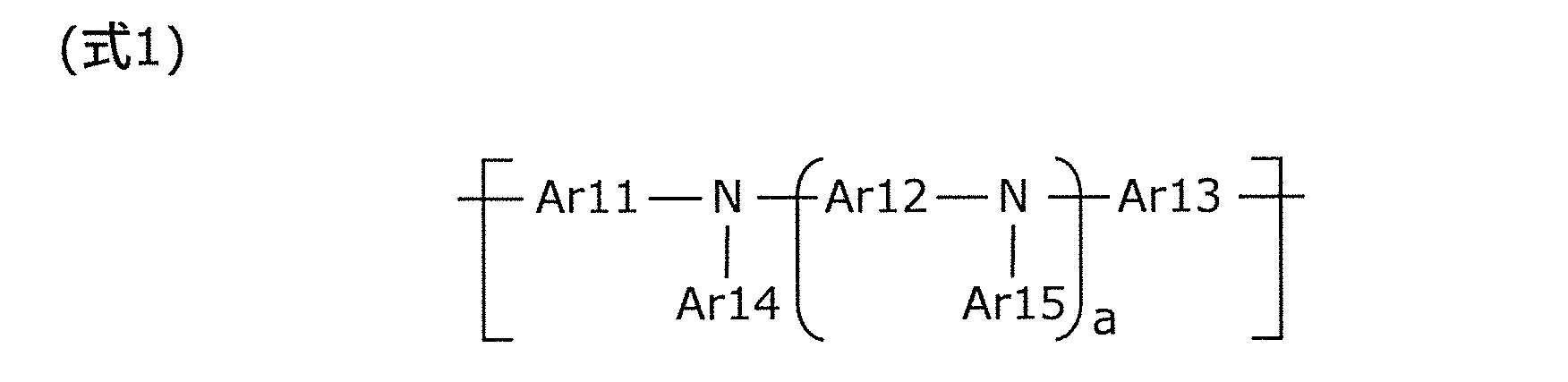
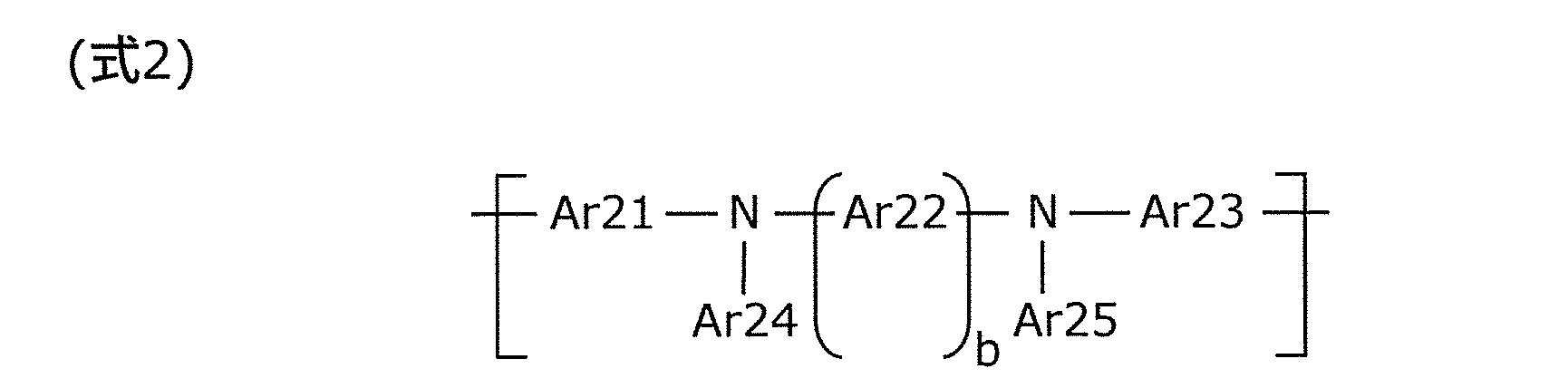
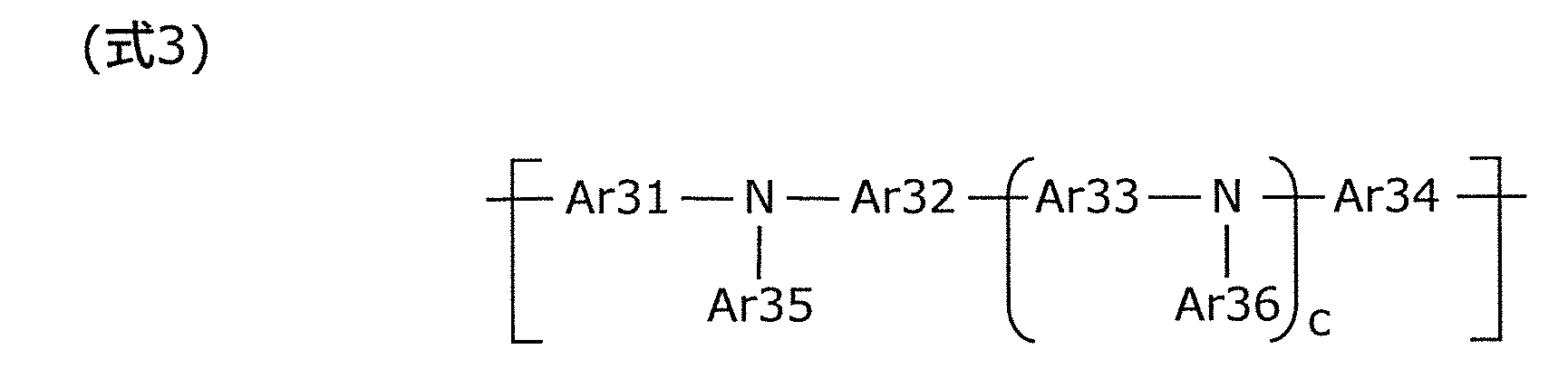
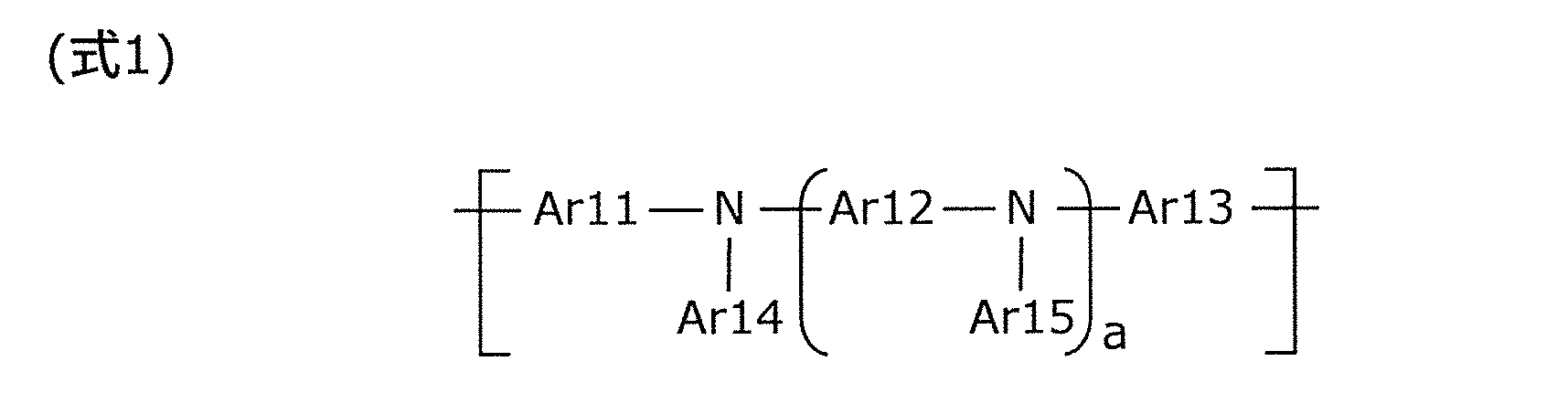
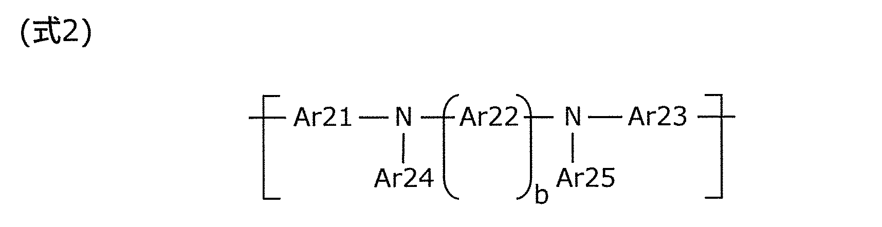
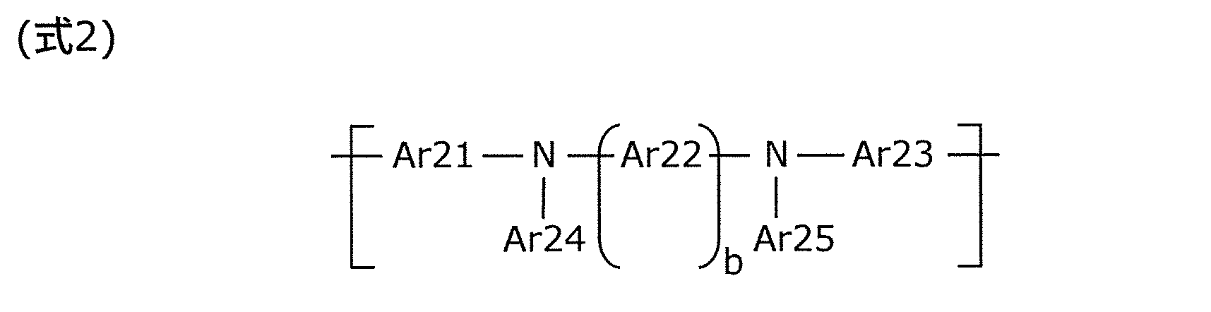
- 1 is a material having (Formula 1), (Formula 2), or (Formula 3) as a structural unit, wherein the structural unit includes an arylamine and does not include fluorene. .
- Ar11 to Ar15 represent the same or different substituted or unsubstituted aromatic groups, and a represents an integer of 0 to 3.
- Ar21 to Ar25 represent the same or different substituted or unsubstituted aromatic groups, and b represents an integer of 0 to 3.
- Ar31 to Ar36 represent the same or different substituted or unsubstituted aromatic groups, and c represents an integer of 0 to 3.
- aromatic group representing Ar11 to Ar15, Ar21 to Ar25, or Ar31 to Ar36 may include a condensed polycyclic structure or a heterocyclic (heterocyclic) structure.
- FIG. 1 is a cross-sectional view of an organic EL element according to an embodiment.
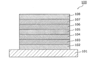
- FIG. 2 is a cross-sectional view of the organic EL element used in this experiment.
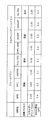
- FIG. 3 is a diagram showing an energy gap of each material, a HOMO (High Occupied Molecular Orbital) level, and a film forming process method of each material used in this experiment.
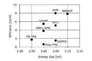
- FIG. 4 is a diagram showing a relationship between the energy gap of each material and the light emission efficiency of the organic EL element when an organic EL element is manufactured using each material of FIG. FIG.
- FIG. 5 shows the HOMO level (energy value) and PL emission quantum yield (PLQE: Photo Luminescence) of each material in the case where a mixed film with the dopant material of the organic light emitting layer is produced using each material of FIG. It is a figure which shows the relationship with Quantum Efficiency.
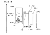
- FIG. 6 is an energy diagram of an organic light emitting layer and a hole transport layer in an organic EL element when “DNTPD” or “Poly-TPD” is used.
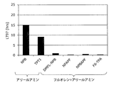
- FIG. 7 is a diagram showing lifetime characteristics of each organic EL element when an organic EL element is manufactured using each material shown in FIG.
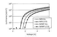
- FIG. 8 is a diagram showing voltage-luminance characteristics before and after the lifetime evaluation of each organic EL element when the organic EL element is manufactured using “NPB” and “NPAPF”.
- FIG. 1 is a cross-sectional view of an organic EL element according to an embodiment.
- the organic EL element 10 includes a substrate 1, a first electrode 2, a hole injection layer 3, an interlayer 4, an organic light emitting layer 5, an electron transport layer 6, and an electron injection layer. 7 and the second electrode 8 are stacked in this order.
- the organic EL element 10 in the present embodiment is a coating type organic EL element in which at least the organic light emitting layer 5 is formed by a coating method.
- the first electrode 2 is formed by a sputtering method
- the hole injection layer 3, the interlayer 4 and the organic light emitting layer 5 are formed by a coating method (printing method).
- the electron injection layer 7 and the second electrode 8 are formed by vapor deposition.
- the substrate 1 is a light transmissive substrate such as a transparent substrate, for example, a glass substrate made of a glass material.
- the substrate 1 is not limited to a glass substrate, but is a translucent resin substrate made of a translucent resin material such as polycarbonate resin or acrylic resin, or a TFT (thin film transistor) substrate that is a backplane of an organic EL display device. There may be.
- the first electrode 2 is a lower electrode and is formed on the substrate 1.
- the first electrode 2 is a transparent electrode having translucency, and for example, a transparent conductive film made of a transparent conductive material such as ITO (Indium Tin Oxide) or IZO (Indium Zinc Oxide) is used.
- the first electrode 2 in the present embodiment is a transparent electrode made of an ITO film.
- the first electrode 2 is an anode (anode).
- the first electrode 2 is not limited to a transparent electrode, and may be a reflective electrode having reflectivity, such as aluminum (Al) or silver (Ag), or an alloy of aluminum or silver, A reflective electrode and a transparent electrode may be laminated.
- the hole injection layer 3 is formed on the first electrode 2.
- the hole injection layer 3 is interposed between the first electrode 2 and the organic light emitting layer 5 and has a function of injecting holes into the organic light emitting layer 5.
- Examples of the material for the hole injection layer 3 include polythiophene derivatives, polyaniline derivatives, polypyrrole derivatives, and the like. Specifically, PEDOT: PSS (mixture of polythiophene and polystyrene sulfonic acid) is used.
- the hole injection layer 3 may be a metal oxide. Specifically, oxides such as tungsten (W), molybdenum (Mo), silver (Ag), chromium (Cr), vanadium (V), nickel (Ni), and iridium (Ir) are used. In the present embodiment, the hole injection layer 3 is PEDOT: PSS.
- the interlayer 4 is formed above the first electrode 2. In the present embodiment, the interlayer 4 is formed on the hole injection layer 3.
- the interlayer 4 is a base layer of the organic light emitting layer 5 and has a cross link function.
- the cross-linking function refers to a function in which a crosslinkable group or an insolubilizing group undergoes a chemical change upon irradiation with energy rays such as heat or ultraviolet light or a combination thereof, and is insolubilized in an organic solvent or water.
- the interlayer 4 is interposed between the hole injection layer 3 and the organic light emitting layer 5, and charges (holes in the present embodiment) injected from the hole injection layer 3 to the organic light emitting layer 5. Has the function of transporting.
- the interlayer 4 is made of a material having a cross-link function.
- the interlayer 4 is made of a material having a larger energy gap (Eg) than the dopant material of the organic light emitting layer 5.
- the interlayer 4 is made of a material having a larger Eg than the host material of the organic light emitting layer 5.
- the energy gap of the material constituting the interlayer 4 is 2.95 eV or more, preferably 3.10 eV or more.
- Eg is an energy difference between the HOMO level and the LUMO (Lowest Unoccupied Molecular Orbital) level.
- Examples of the method for measuring the HOMO level include atmospheric photoelectron spectroscopy, electrochemical techniques (cyclic voltammetry), and photoelectron spectroscopy (PES).
- a method for measuring the LUMO level for example, inverse photoelectron spectroscopy (IPES) or a method of calculating from the energy gap obtained from the absorption edge by light absorption spectroscopy and the HOMO level, etc. Can be mentioned.
- IPES inverse photoelectron spectroscopy
- a method of calculating from the energy gap obtained from the absorption edge by light absorption spectroscopy and the HOMO level etc.
- a method of calculating the HOMO level and the LUMO level by using molecular activation method calculation for each level may be used.
- the interlayer 4 is made of a material having a deeper HOMO level than the dopant material of the organic light emitting layer 5. That is, the HOMO level of the interlayer 4 is made of a material having a higher energy level than the HOMO level of the dopant material of the organic light emitting layer 5. In the present embodiment, the HOMO level of the material constituting the interlayer 4 is substantially the same as the HOMO level of the host material of the organic light emitting layer 5.
- the material of the interlayer 4 for example, a material having the following (formula 1), (formula 2) or (formula 3) as a structural unit can be used.
- the material of the interlayer 4 is a material having at least one of a crosslinkable group or an insolubilizing group and having (Formula 1), (Formula 2) or (Formula 3) as a structural unit, It is a material that contains arylamine in the structural unit and does not contain fluorene.
- Ar11 to Ar15 represent the same or different substituted or unsubstituted aromatic groups, and a represents an integer of 0 to 3.
- Ar21 to Ar25 represent the same or different substituted or unsubstituted aromatic groups, and b represents an integer of 0 to 3.
- Ar31 to Ar36 represent the same or different substituted or unsubstituted aromatic groups, and c represents an integer of 0 to 3.
- aromatic group representing Ar11 to Ar15, Ar21 to Ar25, or Ar31 to Ar36 may include a condensed polycyclic structure or a heterocyclic (heterocyclic) structure.
- the interlayer 4 suppresses charge blocking function that suppresses penetration of charges (electrons in the present embodiment) from the organic light emitting layer 5 to the first electrode 2 side, and suppresses quenching of the excited state of the organic light emitting layer 5. It is good to have a function to do.
- the organic light emitting layer 5 is formed on the interlayer 4. Specifically, the organic light emitting layer 5 is formed by a coating process (coating method) using the interlayer 4 as a base.
- a low molecular material is used as the material of the organic light emitting layer 5.
- the organic light emitting layer 5 is a blue light emitting layer made of a low molecular blue organic light emitting material.
- the low molecular weight material refers to a compound having a molecular weight of 5000 or less.
- the organic light emitting layer 5 is configured such that holes injected from the anode (first electrode 2 in the present embodiment) and electrons injected from the cathode (second electrode 8 in the present embodiment) are organic light emitting. In this layer, recombination in the layer 5 generates excitons and emits light.
- the organic light emitting layer 5 may be composed of a dopant material alone, but more preferably includes a host material and a dopant material.
- the host material mainly has the function of transporting electrons or holes, and the dopant material has the function of light emission.
- the host material is not limited to one type, and may be two or more types.
- the amount of the dopant material may be 0.01% by weight to 30% by weight, and more preferably 0.01% by weight to 10% by weight with respect to the host material.
- the host material of the organic light emitting layer 5 refers to a host material having the smallest energy gap.
- Examples of the host material for the organic light emitting layer 5 include amine compounds, condensed polycyclic aromatic compounds, and heterocyclic compounds.
- amine compound for example, a monoamine derivative, a diamine derivative, a triamine derivative, or a tetraamine derivative is used.
- condensed polycyclic aromatic compound examples include anthracene derivatives, naphthalene derivatives, naphthacene derivatives, phenanthrene derivatives, chrysene derivatives, fluoranthene derivatives, triphenylene derivatives, pentacene derivatives, perylene derivatives, and the like.
- heterocyclic compound examples include carbazole derivatives, furan derivatives, pyridine derivatives, pyrimidine derivatives, triazine derivatives, imidazole derivatives, pyrazole derivatives, triazole derivatives, oxazole derivatives, oxadiazole derivatives, pyrrole derivatives, indole derivatives, azaindole derivatives, And azacarbazole, pyrazoline derivatives, pyrazolone derivatives, phthalocyanine derivatives, and the like.
- the dopant material of the organic light emitting layer 5 for example, pyrene derivatives, fluoranthene derivatives, arylacetylene derivatives, fluorene derivatives, perylene derivatives, oxadiazole derivatives, anthracene derivatives, chrysene derivatives are used.
- a metal complex may be used as a dopant material of the organic light emitting layer 5.
- the metal complex include those having a metal atom and a ligand such as iridium (Ir), platinum (Pt), osmium (Os), gold (Au), rhenium (Re), and ruthenium (Ru). It is done.
- the electron transport layer 6 is formed on the organic light emitting layer 5.
- the electron transport layer 6 is interposed between the organic light emitting layer 5 and the second electrode 8 and has a function of transporting electrons injected from the second electrode 8 to the organic light emitting layer 5.
- the electron transport layer 6 further has a charge blocking function that suppresses penetration of charges (holes in the present embodiment) from the organic light emitting layer 5 to the second electrode 8 side, and an excited state of the organic light emitting layer 5. It is desirable to have a function of suppressing quenching.
- an aromatic heterocyclic compound containing one or more heteroatoms in the molecule is used as the material for the electron transport layer 6, for example.
- the aromatic heterocyclic compound include compounds containing a pyridine ring, a pyrimidine ring, a triazine ring, a benzimidazole ring, a phenanthroline ring, a quinazoline ring or the like in the skeleton.
- the electron injection layer 7 is formed on the electron transport layer 6.
- the electron injection layer 7 is interposed between the electron transport layer 6 and the second electrode 8 and has a function of injecting electrons into the organic light emitting layer 5.
- metal, metal fluoride, or metal oxide As the material of the electron injection layer 7, for example, metal, metal fluoride, or metal oxide is used.
- the metal, metal fluoride, and metal oxide include lithium (Li), sodium (Na), magnesium (Mg), aluminum (Al), potassium (K), cesium (Cs), barium (Ba), and strontium. Examples thereof include metals such as (Sr), fluorides thereof, and oxides thereof.
- a metal complex may be used as a material of the electron injection layer 7.
- metal complexes include 8-quinolinolato sodium, 8-quinolinolato lithium, lithium 2- (2-pyridyl) phenolate, and lithium 2- (2 ′, 2 ′′ -bipyridin-6′-yl) phenolate. Etc.
- the second electrode 8 is formed on the electron transport layer 6.
- the 2nd electrode 8 in this Embodiment is a reflective electrode which has light reflectivity, for example, is a metal electrode formed using the metal material which has reflectivity.
- the second electrode 8 is a cathode (cathode).
- the material of the second electrode 8 for example, aluminum (Al), magnesium (Mg), silver (Ag), aluminum-lithium alloy, magnesium-silver alloy or the like is used.
- the second electrode 8 is not limited to the reflective electrode, and may be a transparent electrode such as an ITO film, like the first electrode 2.
- the organic EL element 10 configured as described above has the first electrode 2 and the first electrode 2. Holes and electrons are respectively injected from the two electrodes 8 into the organic light emitting layer 5. Then, light is generated by combining holes and electrons in the organic light emitting layer 5.
- the organic EL element 10 since the substrate 1 and the first electrode 2 are translucent and the second electrode 8 is reflective, the organic EL element 10 has a bottom emission structure in which light is emitted from the substrate 1 side. is there.
- the organic EL element 10 is not limited to the bottom emission structure, and may have a top emission structure.
- an organic EL element has a structure in which an anode, an organic light emitting layer, and a cathode are laminated on a substrate, and, if necessary, charge injection is performed between the organic light emitting layer and the anode or cathode.
- a charge functional layer such as a layer or a charge transport layer is formed.
- the organic EL element 100 includes a substrate 101, a first electrode (anode) 102, a hole injection layer 103, a hole transport layer 104, an organic light emitting layer 105, and an electron transport.
- the layer 106, the electron injection layer 107, and the second electrode (cathode) 108 are stacked in this order.
- the organic light emitting layer 105 is formed by vapor-depositing an organic light emitting material, for example, a hole injection layer 103, a hole transport layer 104, an organic light emitting layer 105, an electron transport layer 106, an electron injection layer.
- an organic light emitting material for example, a hole injection layer 103, a hole transport layer 104, an organic light emitting layer 105, an electron transport layer 106, an electron injection layer.
- Each of 107 and the second electrode 108 is sequentially formed by an evaporation method.
- the hole injection layer 103 is formed by a coating method (printing method) or a sputtering method
- the hole transport layer 104 and the organic light emitting layer 105 are formed on the hole injection layer 103 by a coating method (printing method)
- the electron transport layer 106 and the electron injection layer 107 are further formed on the organic light emitting layer 105.
- the second electrode (cathode) 108 are formed by vapor deposition.
- the hole transport layer 104 needs to use an interlayer having a cross-link function as a base layer of the organic light emitting layer 105. By doing so, it is possible to prevent the hole transport layer 104 from being dissolved when the organic light emitting layer 105 is formed.
- the material used for the interlayer is, for example, a material having the following (formula 4) as a structural unit and a derivative thereof, and its molecular structure is fluorene and It consists of an arylamine. Furthermore, the material used for the interlayer has a cross-link function. Such a material is characterized by a narrow energy gap and a shallow HOMO level.
- the inventors of the present application have intensively studied an interlayer material capable of obtaining excellent element performance even if it is a coating type organic EL element using a low molecular organic light emitting material as a material of the organic light emitting layer.
- the inventors of the present application evaluated the luminous efficiency of the organic EL element 100 by paying attention to the physical properties of the material constituting the interlayer.
- the organic EL element 100 was produced using the material shown in FIG. 3 as the material of the hole transport layer 104 in FIG. 2, and the light emission efficiency of each organic EL element 100 was evaluated.
- the experiment and the evaluation result will be described.
- FIG. 3 shows the materials used in this experiment, the energy gap and HOMO level of each material, and the film forming process method of each material.
- the HOMO level was measured using atmospheric photoelectron spectroscopy, and the energy gap was determined from the absorption edge wavelength by light absorption spectroscopy.
- NPB is a low-molecular material represented by the following chemical formula (formula 5), and does not contain fluorene but has a structure containing arylamine. “NPB” has an energy gap of 3.05 (eV) and a HOMO level of 5.4 (eV). In this experiment, “NPB” was formed by vapor deposition.
- TPT1 is a low-molecular material represented by the following chemical formula (formula 6), and does not contain fluorene but has a structure containing arylamine. “TPT1” has an energy gap of 3.05 (eV) and a HOMO level of 5.3 (eV). In this experiment, “TPT1” was formed by vapor deposition.
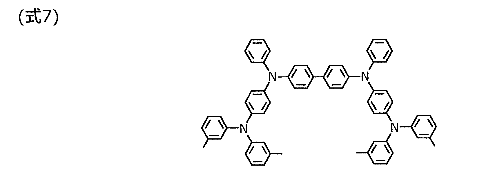
- DNTPD is a low-molecular material represented by the following chemical formula (formula 7), and does not include fluorene but includes arylamine. “DNTPD” has an energy gap of 3.05 (eV) and a HOMO level of 5.1 (eV). In this experiment, “DNTPD” was formed by vapor deposition.
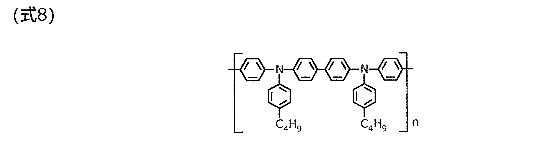
- Poly-TPD is a polymer material having the following (formula 8) as a structural unit, and does not include fluorene but includes arylamine. “Poly-TPD” has an energy gap of 3.00 (eV) and a HOMO level of 5.1 (eV). In this experiment, “Poly-TPD” was formed by a coating method.
- DMFL-NPB is a low molecular material represented by the following chemical formula (formula 9), and has a structure containing fluorene and arylamine. “DMFL-NPB” has an energy gap of 3.00 (eV) and a HOMO level of 5.3 (eV). In this experiment, “DMFL-NPB” was formed by vapor deposition.
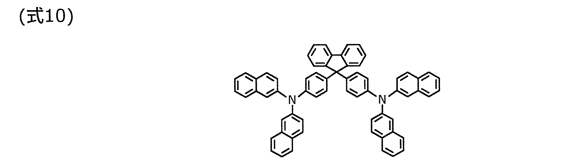
- NPAPF is a low-molecular material represented by the following chemical formula (Formula 10), and has a structure containing fluorene and arylamine. “NPAPF” has an energy gap of 3.00 (eV) and a HOMO level of 5.3 (eV). In this experiment, “NPAPF” was formed by vapor deposition.
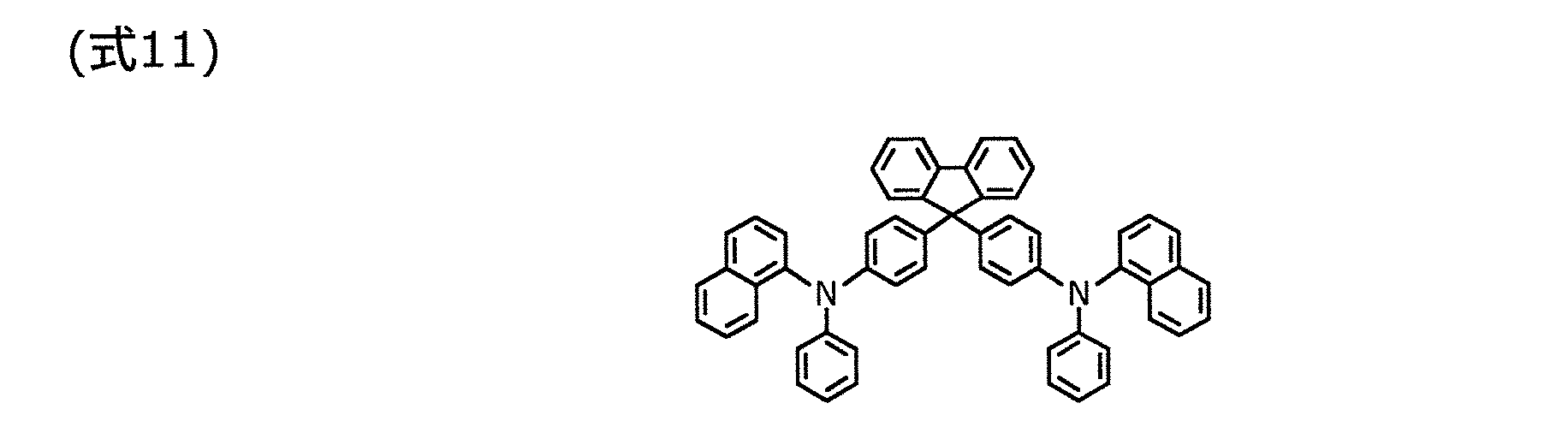
- NPBAPF is a low molecular material represented by the following chemical formula (formula 11), and has a structure containing fluorene and arylamine. “NPBAPF” has an energy gap of 3.10 (eV) and a HOMO level of 5.6 (eV). In this experiment, “NPBAPF” was formed by vapor deposition.
- F8-TPA is a polymer material having the following (formula 12) as a structural unit, and has a structure containing fluorene and arylamine. “F8-TPA” has an energy gap of 2.95 (eV) and a HOMO level of 5.4 (eV). In this experiment, “F8-TPA” was formed by a coating method.
- the organic light-emitting layer includes a host material having an energy gap of 2.95 (eV) and a HOMO level of 5.8 (eV), an energy gap of 2.80 (eV), and a HOMO.
- a dopant material having a level of 5.3 (eV) is used.
- FIG. 4 shows the relationship between the energy gap of each material and the luminous efficiency of the organic EL element when an organic EL element is manufactured using each material of FIG.
- Luminous efficiency of organic EL devices using “F8-TPA”, “DMFL-NPB”, “NPAPF”, “TPT1”, “NPB” and “NPBAPF” in the hole transport layer is large in the energy gap of the material. It can be seen that the higher the energy gap, the higher the luminous efficiency.
- a single-layer PLQE obtained by co-evaporating each material shown in FIG. 3 except the polymer materials “F8-TPA” and “Poly-TPD” and the dopant material of the organic light emitting layer at a film formation rate ratio of 1: 1. was measured.
- PLQE is the ratio between the number of photons absorbed by the material and the number of photons emitted from the material when the single layer film set in the integrating sphere is irradiated with excitation light.
- FIG. 5 shows the relationship between the HOMO level of each of the materials and PLQE.
- the HOMO level is shallower than the dopant material of the organic light-emitting layer, and the PLQE value is lowered only by the “DNTPD” co-deposited film. It was. In this PLQE evaluation, 420 nm excitation light was used to selectively excite the dopant.
- FIG. 6 is an energy diagram of an organic light-emitting layer and a hole transport layer in an organic EL element when “DNTPD” or “Poly-TPD” is used as the hole transport layer.
- the organic EL element when the HOMO level of the hole transport layer is shallower than the HOMO level of the dopant material of the organic light emitting layer, at the interface between the hole transport layer and the organic light emitting layer. Then, an exciplex is formed between two molecules of the host material of the organic light emitting layer and the material of the hole transport layer, and light emission or quenching is performed.
- the materials having low luminous efficiency (“DNTPD” and “Poly-TPD”) are considered to have formed an exciplex with the organic light emitting layer 105 because the HOMO level is shallow. As a result, it is considered that the luminous efficiency is lowered.
- the inventors of the present application have used a material having a desired energy gap and a desired HOMO level as an underlying layer of the organic light emitting layer.
- the inventors have found that energy transfer from the organic light emitting layer to the interlayer can be suppressed to suppress quenching between the organic light emitting layer and the interlayer, thereby improving luminous efficiency.
- the dopant of the organic light emitting layer 5 It has been found that an organic EL element having excellent luminous efficiency can be realized by using the interlayer 4 having a material having an energy gap larger than that of the material and deeper than the HOMO level of the dopant material of the organic light emitting layer 5.
- the energy gap of the material constituting the interlayer 4 should be larger than the energy gap of the host material of the organic light emitting layer 5.
- the energy gap of the material constituting the interlayer 4 is preferably 2.95 eV or more.
- the luminous efficiency is saturated when the energy gap is 3.10 eV or more, and the energy gap of the material constituting the interlayer 4 is further preferably 3.10 eV or more.
- the HOMO level of the material constituting the interlayer 4 should be substantially the same as the HOMO level of the host material of the organic light emitting layer 5 in order to reliably obtain an organic EL element with high luminous efficiency. .
- the organic EL element 10 even if it is a coating type organic EL element using a low-molecular organic light-emitting material for the organic light-emitting layer 5, the dopant material of the organic light-emitting layer 5 is used.
- the interlayer 4 made of a material having a large energy gap and deeper than the HOMO level of the dopant material of the organic light emitting layer 5, an organic EL element having high light emission efficiency can be realized.
- the inventors of the present application focused on the material constituting the interlayer and evaluated the lifetime characteristics of the organic EL element 100.
- FIG. 7 is a diagram showing the lifetime characteristics of each organic EL element when an organic EL element is produced using each material shown in FIG.
- LT97 represents a life characteristic, and represents the time required for the luminance to decrease to 97% with the initial luminance set to 100%.
- an organic EL device manufactured using a material containing both fluorene and arylamine (“DMFL-NPB”, “NPAPPF”, “NPBAPF”, “F8-TPA”) has a short lifetime.
- an organic EL element manufactured using a material (“NPB”, “TPT1”) that does not contain fluorene and contains an arylamine has a long lifetime.
- the lifetime of the organic EL device using a material containing arylamine (“NPB”, “TPT1”) that does not contain fluorene is the material containing “fluorene and arylamine” (“DMFL-NPB”, “ NPAPF ”,“ NPBAPF ”) is used, and the lifetime of the organic EL element is about 10 times or more.
- FIG. 8 is a diagram showing voltage-luminance characteristics before and after the lifetime evaluation of each organic EL element when the organic EL element is manufactured using “NPB” and “NPAPF”.
- NPAPF a material containing fluorene and arylamine.
- the voltage required to obtain a luminance of 1000 cd / m 2 is an organic EL element manufactured using “NPB” which is a material that does not contain fluorene but contains arylamine.
- the organic EL element fabricated using “NPAPF” which is a material containing fluorene and arylamine is increased by 0.6V.
- the organic EL element using “NPAPF” containing fluorene and arylamine has the same brightness as the organic EL element using “NPB” containing no aryl and containing fluorene.
- the amount of increase in required voltage is large.
- the emission ability of the light emitting layer is decreased, whereas fluorene and
- an organic EL device manufactured using “NPAPPF” which is a material containing an arylamine it is considered that not only the light emission capability of the light emitting layer is lowered but also “NPAPPF” itself is deteriorated. More specifically, it is considered that the fluorene portion of “NPAPF” is deteriorated due to the energization of the life evaluation.
- the present inventors have determined that the lifetime of the organic EL element can be reduced by configuring the interlayer material that is the base of the organic light emitting layer not to contain fluorene. The knowledge that the fall of can be suppressed was acquired.
- the material of the layer 4 is a material having at least one of a crosslinkable group and an insolubilizing group and having the above (Formula 1), (Formula 2), or (Formula 3) as a structural unit, It has been found that an organic EL device having a long lifetime can be realized by using a material containing arylamine and not containing fluorene.
- the organic EL element 10 even if it is a coating type organic EL element using a low-molecular organic light-emitting material for the organic light-emitting layer 5, at least a crosslinkable group and an insolubilizing group are present.
- the layer 4 an organic EL element having a long lifetime can be realized.
- the material of the interlayer 4 has a cross-link function, it is possible to suppress the dissolution of the interlayer 4 when the organic light emitting layer 5 is formed by a coating method.
- a long organic EL element can be realized.
- the material of the interlayer 4 has a larger energy gap than the dopant material of the organic light emitting layer 5 and the HOMO level of the dopant material of the organic light emitting layer 5.
- a material containing an arylamine as a structural unit and not containing fluorene may be used as the interlayer 4.
- the organic EL element 10 As described above, according to the organic EL element 10 according to the present embodiment, it is possible to obtain an organic EL element having high element performance even if it is a coating type organic EL element using a low molecular organic light emitting material for an organic light emitting layer. Can do.
- the organic EL element 10 configured as described above can be used for a display device, for example.
- an organic EL display device can be realized by forming the organic EL element 10 in each of a plurality of pixels arranged in a matrix.
- an RGB full-color organic EL display device can be realized by changing the organic light emitting material of the organic light emitting layer of the organic EL element constituting one pixel for each element.
- the organic EL display device may be driven by either a passive matrix driving method or an active matrix driving method.
- the organic light emitting layer 5 made of a low molecular material is formed by a coating method, but may be formed by a vapor deposition method.
- the first electrode 2 is formed by a sputtering method
- the hole injection layer 3 is formed by a coating method or a sputtering method
- the electron transport layer 6, the electron injection layer 7 and the second electrode 8 are deposited.
- the organic EL element is used for a display device.
- the organic EL element 10 in the above embodiment can be used for a light emitting device other than the display device.
- the organic EL element can be used in a lighting device such as an organic EL lighting panel.
- the technology of the present disclosure is useful for an organic EL element and a display device, for example, a display device such as a television receiver, a monitor display, a digital signage, a portable terminal or a tablet terminal, or a lighting device such as a ceiling light or indirect illumination. It can be widely used for various light emitting devices.
- a display device such as a television receiver, a monitor display, a digital signage, a portable terminal or a tablet terminal, or a lighting device such as a ceiling light or indirect illumination. It can be widely used for various light emitting devices.
Landscapes
- Engineering & Computer Science (AREA)
- Chemical & Material Sciences (AREA)
- Materials Engineering (AREA)
- Physics & Mathematics (AREA)
- Spectroscopy & Molecular Physics (AREA)
- Optics & Photonics (AREA)
- Organic Chemistry (AREA)
- Manufacturing & Machinery (AREA)
- General Physics & Mathematics (AREA)
- Theoretical Computer Science (AREA)
- Electromagnetism (AREA)
- Electroluminescent Light Sources (AREA)
- Devices For Indicating Variable Information By Combining Individual Elements (AREA)
Abstract
Description


[有機EL素子の構成]
まず、実施の形態に係る有機EL素子10について、図1を用いて説明する。図1は、実施の形態に係る有機EL素子の断面図である。

次に、本実施の形態に係る有機EL素子10の特徴について、本開示の技術に至った経緯も含めて説明する。




以上、有機EL素子及び表示装置について、実施の形態に基づいて説明したが、本開示の技術は、上記実施の形態に限定されるものではない。
1、101 基板
2、102 第1電極
3、103 正孔注入層
4 インターレイヤー
5、105 有機発光層
6、106 電子輸送層
7、107 電子注入層
8、108 第2電極
104 正孔輸送層
Claims (22)
- 第1電極と、
前記第1電極の上方に形成されたインターレイヤーと、
前記インターレイヤーを下地として形成された有機発光層と、
前記有機発光層の上方に形成された第2電極とを備え、
前記有機発光層は、少なくともホスト材料とドーパント材料とを含み、
前記インターレイヤーは、前記ドーパント材料よりもエネルギーギャップが大きく、かつ、前記ドーパント材料のHOMO準位よりも深い材料で構成されている
有機EL素子。 - 前記ホスト材料及び前記ドーパント材料は、低分子材料である
請求項1に記載の有機EL素子。 - 前記インターレイヤーを構成する材料のエネルギーギャップは、前記ホスト材料のエネルギーギャップよりも大きい
請求項1又は2に記載の有機EL素子。 - 前記インターレイヤーを構成する材料のエネルギーギャップは、2.95eV以上である
請求項3に記載の有機EL素子。 - 前記インターレイヤーを構成する材料のエネルギーギャップは、3.10eV以上である
請求項3に記載の有機EL素子。 - 前記インターレイヤーを構成する材料のHOMO準位は、前記ホスト材料のHOMO準位と同等である
請求項3~5のいずれか1項に記載の有機EL素子。 - 前記インターレイヤーは、クロスリンク機能を有し、塗布法で形成される
請求項3~6のいずれか1項に記載の有機EL素子。 - 前記有機発光層は、塗布法で形成される
請求項7に記載の有機EL素子。 - 第1電極と、
前記第1電極の上方に形成されたインターレイヤーと、
前記インターレイヤーを下地として形成された有機発光層と、
前記有機発光層の上方に形成された第2電極とを備え、
前記有機発光層は、少なくともホスト材料とドーパント材料とを含み、
前記インターレイヤーの材料は、架橋性基及び不溶化基の少なくとも1つを有し、(式1)を構成単位とする材料であって、アリールアミンを含み、かつ、フルオレンを含まない
有機EL素子。
- 第1電極と、
前記第1電極の上方に形成されたインターレイヤーと、
前記インターレイヤーを下地として形成された有機発光層と、
前記有機発光層の上方に形成された第2電極とを備え、
前記有機発光層は、少なくともホスト材料とドーパント材料とを含み、
前記インターレイヤーの材料は、架橋性基及び不溶化基の少なくとも1つを有し、(式2)を構成単位とする材料であって、アリールアミンを含み、かつ、フルオレンを含まない
有機EL素子。
- 第1電極と、
前記第1電極の上方に形成されたインターレイヤーと、
前記インターレイヤーを下地として形成された有機発光層と、
前記有機発光層の上方に形成された第2電極とを備え、
前記有機発光層は、少なくともホスト材料とドーパント材料とを含み、
前記インターレイヤーの材料は、架橋性基及び不溶化基の少なくとも1つを有し、(式3)を構成単位とする材料であって、アリールアミンを含み、かつ、フルオレンを含まない
有機EL素子。

- 前記ホスト材料及び前記ドーパント材料は、低分子材料である
請求項9~11のいずれか1項に記載の有機EL素子。 - 前記芳香族基は、縮合多環構造を含む
請求項12に記載の有機EL素子。 - 前記芳香族基は、ヘテロ環構造を含む
請求項12に記載の有機EL素子。 - 前記有機発光層は、塗布法で形成される
請求項9~14のいずれか1項に記載の有機EL素子。 - 前記インターレイヤーの材料は、架橋性基及び不溶化基の少なくとも1つを有し、(式1)を構成単位とする材料であって、アリールアミンを含み、かつ、フルオレンを含まない
請求項1~6のいずれか1項に記載の有機EL素子。

- 前記インターレイヤーの材料は、架橋性基及び不溶化基の少なくとも1つを有し、(式2)を構成単位とする材料であって、アリールアミンを含み、かつ、フルオレンを含まない
請求項1~6のいずれか1項に記載の有機EL素子。
- 前記インターレイヤーの材料は、架橋性基及び不溶化基の少なくとも1つを有し、(式3)を構成単位とする材料であって、アリールアミンを含み、かつ、フルオレンを含まない
請求項1~6のいずれか1項に記載の有機EL素子。

- 前記芳香族基は、縮合多環構造を含む
請求項16~18のいずれか1項に記載の有機EL素子。 - 前記芳香族基は、ヘテロ環構造を含む
請求項16~18のいずれか1項に記載の有機EL素子。 - 前記有機発光層は、塗布法で形成される
請求項16~20のいずれか1項に記載の有機EL素子。 - 請求項1~21のいずれか1項に記載の有機EL素子を備える
表示装置。
Priority Applications (3)
| Application Number | Priority Date | Filing Date | Title |
|---|---|---|---|
| JP2016560061A JPWO2016079985A1 (ja) | 2014-11-17 | 2015-11-17 | 有機el素子及び表示装置 |
| US15/526,574 US10892429B2 (en) | 2014-11-17 | 2015-11-17 | Organic EL element and display device |
| KR1020177012533A KR101946738B1 (ko) | 2014-11-17 | 2015-11-17 | 유기 el 소자 및 표시 장치 |
Applications Claiming Priority (4)
| Application Number | Priority Date | Filing Date | Title |
|---|---|---|---|
| JP2014-232875 | 2014-11-17 | ||
| JP2014232875 | 2014-11-17 | ||
| JP2014232827 | 2014-11-17 | ||
| JP2014-232827 | 2014-11-17 |
Publications (1)
| Publication Number | Publication Date |
|---|---|
| WO2016079985A1 true WO2016079985A1 (ja) | 2016-05-26 |
Family
ID=56013558
Family Applications (1)
| Application Number | Title | Priority Date | Filing Date |
|---|---|---|---|
| PCT/JP2015/005748 Ceased WO2016079985A1 (ja) | 2014-11-17 | 2015-11-17 | 有機el素子及び表示装置 |
Country Status (4)
| Country | Link |
|---|---|
| US (1) | US10892429B2 (ja) |
| JP (1) | JPWO2016079985A1 (ja) |
| KR (1) | KR101946738B1 (ja) |
| WO (1) | WO2016079985A1 (ja) |
Citations (5)
| Publication number | Priority date | Publication date | Assignee | Title |
|---|---|---|---|---|
| JP2005285749A (ja) * | 2004-03-03 | 2005-10-13 | Tosoh Corp | トリアリールアミンポリマー及びその製造方法 |
| US20070069636A1 (en) * | 2005-09-28 | 2007-03-29 | Choulis Stelios A | Organic electrophosphorescence device |
| JP2010189454A (ja) * | 2009-02-13 | 2010-09-02 | Mitsubishi Chemicals Corp | 共役ポリマー、ポリマー組成物、電荷輸送材料、有機電界発光素子、有機elディスプレイ及び有機el照明 |
| WO2011071169A1 (ja) * | 2009-12-11 | 2011-06-16 | 三菱化学株式会社 | 有機電界発光素子、有機el表示装置及び有機el照明 |
| JP2014187130A (ja) * | 2013-03-22 | 2014-10-02 | Nippon Hoso Kyokai <Nhk> | 有機エレクトロルミネッセンス素子、表示装置および照明装置、正孔輸送材料の評価方法 |
Family Cites Families (3)
| Publication number | Priority date | Publication date | Assignee | Title |
|---|---|---|---|---|
| TWI365218B (en) | 2003-11-17 | 2012-06-01 | Sumitomo Chemical Co | Conjugated oligomers or polymers based on crosslinkable arylamine compounds |
| JP2006190759A (ja) | 2005-01-05 | 2006-07-20 | Idemitsu Kosan Co Ltd | 有機エレクトロルミネッセンス素子 |
| TW201204687A (en) | 2010-06-17 | 2012-02-01 | Du Pont | Electroactive materials |
-
2015
- 2015-11-17 JP JP2016560061A patent/JPWO2016079985A1/ja active Pending
- 2015-11-17 KR KR1020177012533A patent/KR101946738B1/ko active Active
- 2015-11-17 US US15/526,574 patent/US10892429B2/en active Active
- 2015-11-17 WO PCT/JP2015/005748 patent/WO2016079985A1/ja not_active Ceased
Patent Citations (5)
| Publication number | Priority date | Publication date | Assignee | Title |
|---|---|---|---|---|
| JP2005285749A (ja) * | 2004-03-03 | 2005-10-13 | Tosoh Corp | トリアリールアミンポリマー及びその製造方法 |
| US20070069636A1 (en) * | 2005-09-28 | 2007-03-29 | Choulis Stelios A | Organic electrophosphorescence device |
| JP2010189454A (ja) * | 2009-02-13 | 2010-09-02 | Mitsubishi Chemicals Corp | 共役ポリマー、ポリマー組成物、電荷輸送材料、有機電界発光素子、有機elディスプレイ及び有機el照明 |
| WO2011071169A1 (ja) * | 2009-12-11 | 2011-06-16 | 三菱化学株式会社 | 有機電界発光素子、有機el表示装置及び有機el照明 |
| JP2014187130A (ja) * | 2013-03-22 | 2014-10-02 | Nippon Hoso Kyokai <Nhk> | 有機エレクトロルミネッセンス素子、表示装置および照明装置、正孔輸送材料の評価方法 |
Also Published As
| Publication number | Publication date |
|---|---|
| KR101946738B1 (ko) | 2019-02-11 |
| US10892429B2 (en) | 2021-01-12 |
| JPWO2016079985A1 (ja) | 2017-08-17 |
| US20170309854A1 (en) | 2017-10-26 |
| KR20170070113A (ko) | 2017-06-21 |
Similar Documents
| Publication | Publication Date | Title |
|---|---|---|
| CN104409648B (zh) | 串联式有机发光二极管及显示器 | |
| US10553650B2 (en) | Organic electroluminescent element, organic electroluminescent panel, and luminescent unit comprising a film thickness adjustment layer positioned outside of a resonator | |
| JP5694019B2 (ja) | 有機電界発光素子、表示装置および照明装置 | |
| US11930651B2 (en) | Organic luminescent material, organic electroluminescent element and display device | |
| US10141384B2 (en) | Organic electroluminescent panel and luminescent unit | |
| JP2023065580A (ja) | 有機エレクトロルミネセントデバイス | |
| CN101379884A (zh) | 有机电致发光元件 | |
| WO2009130858A1 (ja) | 有機エレクトロルミネッセンス素子 | |
| TW201230434A (en) | Organic electronic device with composite electrode | |
| CN102456844A (zh) | 有机发光二极管及其制造方法 | |
| JP5330429B2 (ja) | 有機電界発光素子、表示装置および照明装置 | |
| JP6770900B2 (ja) | 有機エレクトロルミネッセンス素子 | |
| Vasilopoulou et al. | Solution processed multi-color organic light emitting diodes for application in telecommunications | |
| KR101946738B1 (ko) | 유기 el 소자 및 표시 장치 | |
| Gaur et al. | MgF2 as an interlayer to enhance the stability of thermally activated delayed fluorescence based organic electroluminescence devices | |
| JP2019021903A (ja) | 有機電界発光素子、有機電界発光装置および電子機器 | |
| JP2015109370A (ja) | 電界発光素子 | |
| JP7834653B2 (ja) | 表示素子及び表示装置 | |
| JP2019175665A (ja) | 有機電界発光素子 | |
| JP2010212675A (ja) | 有機電界発光素子、有機elディスプレイ、有機el照明及び有機el信号装置 | |
| JP6803727B2 (ja) | 有機エレクトロルミネッセンス素子 | |
| JP6770899B2 (ja) | 有機エレクトロルミネッセンス素子 | |
| US10476022B2 (en) | Organic light emitting diode and manufacturing method thereof, display apparatus | |
| JP2018190804A (ja) | 有機電界発光素子、有機電界発光装置、電子機器および、有機電界発光素子の製造方法 | |
| Wang et al. | Phosphorescent Molecularly Doped Light‐Emitting Diodes with Blended Polymer Host and Wide Emission Spectra |
Legal Events
| Date | Code | Title | Description |
|---|---|---|---|
| 121 | Ep: the epo has been informed by wipo that ep was designated in this application |
Ref document number: 15860467 Country of ref document: EP Kind code of ref document: A1 |
|
| ENP | Entry into the national phase |
Ref document number: 2016560061 Country of ref document: JP Kind code of ref document: A |
|
| ENP | Entry into the national phase |
Ref document number: 20177012533 Country of ref document: KR Kind code of ref document: A |
|
| WWE | Wipo information: entry into national phase |
Ref document number: 15526574 Country of ref document: US |
|
| NENP | Non-entry into the national phase |
Ref country code: DE |
|
| 122 | Ep: pct application non-entry in european phase |
Ref document number: 15860467 Country of ref document: EP Kind code of ref document: A1 |